WO2020054018A1 - Procédé d'évaluation de la perméabilité aux anions d'un film contenant du graphène et élément de conversion photoélectrique - Google Patents
Procédé d'évaluation de la perméabilité aux anions d'un film contenant du graphène et élément de conversion photoélectrique Download PDFInfo
- Publication number
- WO2020054018A1 WO2020054018A1 PCT/JP2018/033968 JP2018033968W WO2020054018A1 WO 2020054018 A1 WO2020054018 A1 WO 2020054018A1 JP 2018033968 W JP2018033968 W JP 2018033968W WO 2020054018 A1 WO2020054018 A1 WO 2020054018A1
- Authority
- WO
- WIPO (PCT)
- Prior art keywords
- graphene
- electrode
- working electrode
- containing film
- film
- Prior art date
Links
- OKTJSMMVPCPJKN-UHFFFAOYSA-N Carbon Chemical compound [C] OKTJSMMVPCPJKN-UHFFFAOYSA-N 0.000 title claims abstract description 183
- 229910021389 graphene Inorganic materials 0.000 title claims abstract description 176
- 238000006243 chemical reaction Methods 0.000 title claims abstract description 96
- 150000001450 anions Chemical class 0.000 title claims abstract description 50
- 238000000034 method Methods 0.000 title claims abstract description 42
- 230000035699 permeability Effects 0.000 title claims abstract description 20
- 229910052709 silver Inorganic materials 0.000 claims abstract description 73
- 239000004332 silver Substances 0.000 claims abstract description 73
- 239000007864 aqueous solution Substances 0.000 claims abstract description 57
- 238000005259 measurement Methods 0.000 claims abstract description 16
- 238000010408 sweeping Methods 0.000 claims abstract description 11
- 239000010408 film Substances 0.000 claims description 168
- BQCADISMDOOEFD-UHFFFAOYSA-N Silver Chemical compound [Ag] BQCADISMDOOEFD-UHFFFAOYSA-N 0.000 claims description 88
- 125000004433 nitrogen atom Chemical group N* 0.000 claims description 18
- 239000002042 Silver nanowire Substances 0.000 claims description 17
- 125000004432 carbon atom Chemical group C* 0.000 claims description 15
- -1 halogen ion Chemical class 0.000 claims description 15
- 239000010409 thin film Substances 0.000 claims description 14
- 125000000217 alkyl group Chemical group 0.000 claims description 12
- 239000000203 mixture Substances 0.000 claims description 9
- 229910052736 halogen Inorganic materials 0.000 claims description 8
- 125000001424 substituent group Chemical group 0.000 claims description 7
- 229910044991 metal oxide Inorganic materials 0.000 claims description 6
- 150000004706 metal oxides Chemical class 0.000 claims description 6
- 239000012528 membrane Substances 0.000 claims description 5
- 230000001681 protective effect Effects 0.000 claims description 3
- XLYOFNOQVPJJNP-UHFFFAOYSA-M hydroxide Chemical compound [OH-] XLYOFNOQVPJJNP-UHFFFAOYSA-M 0.000 claims description 2
- 239000000243 solution Substances 0.000 abstract description 9
- 230000010220 ion permeability Effects 0.000 abstract description 6
- 239000010410 layer Substances 0.000 description 91
- OAKJQQAXSVQMHS-UHFFFAOYSA-N Hydrazine Chemical compound NN OAKJQQAXSVQMHS-UHFFFAOYSA-N 0.000 description 28
- XKRFYHLGVUSROY-UHFFFAOYSA-N Argon Chemical compound [Ar] XKRFYHLGVUSROY-UHFFFAOYSA-N 0.000 description 18
- KFZMGEQAYNKOFK-UHFFFAOYSA-N Isopropanol Chemical compound CC(C)O KFZMGEQAYNKOFK-UHFFFAOYSA-N 0.000 description 18
- 229920002799 BoPET Polymers 0.000 description 17
- 229910001316 Ag alloy Inorganic materials 0.000 description 16
- 239000007789 gas Substances 0.000 description 15
- 125000004122 cyclic group Chemical group 0.000 description 14
- 238000010438 heat treatment Methods 0.000 description 14
- FAPWRFPIFSIZLT-UHFFFAOYSA-M Sodium chloride Chemical compound [Na+].[Cl-] FAPWRFPIFSIZLT-UHFFFAOYSA-M 0.000 description 12
- 239000006185 dispersion Substances 0.000 description 12
- 239000002244 precipitate Substances 0.000 description 12
- QGZKDVFQNNGYKY-UHFFFAOYSA-N Ammonia Chemical compound N QGZKDVFQNNGYKY-UHFFFAOYSA-N 0.000 description 10
- GWEVSGVZZGPLCZ-UHFFFAOYSA-N Titan oxide Chemical compound O=[Ti]=O GWEVSGVZZGPLCZ-UHFFFAOYSA-N 0.000 description 10
- 230000004888 barrier function Effects 0.000 description 10
- 238000005229 chemical vapour deposition Methods 0.000 description 10
- VNWKTOKETHGBQD-UHFFFAOYSA-N methane Chemical compound C VNWKTOKETHGBQD-UHFFFAOYSA-N 0.000 description 10
- VEXZGXHMUGYJMC-UHFFFAOYSA-M Chloride anion Chemical compound [Cl-] VEXZGXHMUGYJMC-UHFFFAOYSA-M 0.000 description 9
- 229920002873 Polyethylenimine Polymers 0.000 description 9
- YXFVVABEGXRONW-UHFFFAOYSA-N Toluene Chemical compound CC1=CC=CC=C1 YXFVVABEGXRONW-UHFFFAOYSA-N 0.000 description 9
- 238000004833 X-ray photoelectron spectroscopy Methods 0.000 description 9
- 229910052786 argon Inorganic materials 0.000 description 9
- 239000002356 single layer Substances 0.000 description 9
- 238000004544 sputter deposition Methods 0.000 description 9
- XLOMVQKBTHCTTD-UHFFFAOYSA-N Zinc monoxide Chemical compound [Zn]=O XLOMVQKBTHCTTD-UHFFFAOYSA-N 0.000 description 8
- 238000010586 diagram Methods 0.000 description 8
- 239000004065 semiconductor Substances 0.000 description 8
- XLYOFNOQVPJJNP-UHFFFAOYSA-N water Substances O XLYOFNOQVPJJNP-UHFFFAOYSA-N 0.000 description 8
- RYGMFSIKBFXOCR-UHFFFAOYSA-N Copper Chemical compound [Cu] RYGMFSIKBFXOCR-UHFFFAOYSA-N 0.000 description 7
- 229910045601 alloy Inorganic materials 0.000 description 7
- 239000000956 alloy Substances 0.000 description 7
- 239000010949 copper Substances 0.000 description 7
- 230000006866 deterioration Effects 0.000 description 7
- 239000001257 hydrogen Substances 0.000 description 7
- 229910052739 hydrogen Inorganic materials 0.000 description 7
- IJGRMHOSHXDMSA-UHFFFAOYSA-N Atomic nitrogen Chemical compound N#N IJGRMHOSHXDMSA-UHFFFAOYSA-N 0.000 description 6
- RTAQQCXQSZGOHL-UHFFFAOYSA-N Titanium Chemical compound [Ti] RTAQQCXQSZGOHL-UHFFFAOYSA-N 0.000 description 6
- 239000000872 buffer Substances 0.000 description 6
- MVPPADPHJFYWMZ-UHFFFAOYSA-N chlorobenzene Chemical compound ClC1=CC=CC=C1 MVPPADPHJFYWMZ-UHFFFAOYSA-N 0.000 description 6
- 229910052751 metal Inorganic materials 0.000 description 6
- 239000002184 metal Substances 0.000 description 6
- 229920000301 poly(3-hexylthiophene-2,5-diyl) polymer Polymers 0.000 description 6
- 229920001296 polysiloxane Polymers 0.000 description 6
- 239000011780 sodium chloride Substances 0.000 description 6
- 238000004528 spin coating Methods 0.000 description 6
- XOLBLPGZBRYERU-UHFFFAOYSA-N tin dioxide Chemical compound O=[Sn]=O XOLBLPGZBRYERU-UHFFFAOYSA-N 0.000 description 6
- 229910001887 tin oxide Inorganic materials 0.000 description 6
- OGIDPMRJRNCKJF-UHFFFAOYSA-N titanium oxide Inorganic materials [Ti]=O OGIDPMRJRNCKJF-UHFFFAOYSA-N 0.000 description 6
- 238000012546 transfer Methods 0.000 description 6
- 229910021529 ammonia Inorganic materials 0.000 description 5
- 238000009792 diffusion process Methods 0.000 description 5
- 230000000694 effects Effects 0.000 description 5
- 229910052737 gold Inorganic materials 0.000 description 5
- 239000010931 gold Substances 0.000 description 5
- 125000004435 hydrogen atom Chemical class [H]* 0.000 description 5
- 150000002500 ions Chemical class 0.000 description 5
- 229910001220 stainless steel Inorganic materials 0.000 description 5
- 239000010935 stainless steel Substances 0.000 description 5
- 239000000758 substrate Substances 0.000 description 5
- NWZSZGALRFJKBT-KNIFDHDWSA-N (2s)-2,6-diaminohexanoic acid;(2s)-2-hydroxybutanedioic acid Chemical compound OC(=O)[C@@H](O)CC(O)=O.NCCCC[C@H](N)C(O)=O NWZSZGALRFJKBT-KNIFDHDWSA-N 0.000 description 4
- 238000000137 annealing Methods 0.000 description 4
- 239000003638 chemical reducing agent Substances 0.000 description 4
- 229910052802 copper Inorganic materials 0.000 description 4
- ORTQZVOHEJQUHG-UHFFFAOYSA-L copper(II) chloride Chemical compound Cl[Cu]Cl ORTQZVOHEJQUHG-UHFFFAOYSA-L 0.000 description 4
- 239000011888 foil Substances 0.000 description 4
- IKDUDTNKRLTJSI-UHFFFAOYSA-N hydrazine monohydrate Substances O.NN IKDUDTNKRLTJSI-UHFFFAOYSA-N 0.000 description 4
- 239000000463 material Substances 0.000 description 4
- 239000002245 particle Substances 0.000 description 4
- 229920000139 polyethylene terephthalate Polymers 0.000 description 4
- 239000005020 polyethylene terephthalate Substances 0.000 description 4
- 239000011787 zinc oxide Substances 0.000 description 4
- VEXZGXHMUGYJMC-UHFFFAOYSA-N Hydrochloric acid Chemical compound Cl VEXZGXHMUGYJMC-UHFFFAOYSA-N 0.000 description 3
- 229920001609 Poly(3,4-ethylenedioxythiophene) Polymers 0.000 description 3
- 238000000026 X-ray photoelectron spectrum Methods 0.000 description 3
- 239000012790 adhesive layer Substances 0.000 description 3
- 239000012298 atmosphere Substances 0.000 description 3
- QVGXLLKOCUKJST-UHFFFAOYSA-N atomic oxygen Chemical compound [O] QVGXLLKOCUKJST-UHFFFAOYSA-N 0.000 description 3
- 150000001768 cations Chemical class 0.000 description 3
- 239000000919 ceramic Substances 0.000 description 3
- 230000008859 change Effects 0.000 description 3
- 230000000052 comparative effect Effects 0.000 description 3
- 150000001875 compounds Chemical class 0.000 description 3
- 239000013078 crystal Substances 0.000 description 3
- 238000002484 cyclic voltammetry Methods 0.000 description 3
- 238000000151 deposition Methods 0.000 description 3
- 239000011521 glass Substances 0.000 description 3
- PCHJSUWPFVWCPO-UHFFFAOYSA-N gold Chemical compound [Au] PCHJSUWPFVWCPO-UHFFFAOYSA-N 0.000 description 3
- 230000036571 hydration Effects 0.000 description 3
- 238000006703 hydration reaction Methods 0.000 description 3
- 238000002329 infrared spectrum Methods 0.000 description 3
- 230000003993 interaction Effects 0.000 description 3
- 229910052757 nitrogen Inorganic materials 0.000 description 3
- 239000011368 organic material Substances 0.000 description 3
- 239000001301 oxygen Substances 0.000 description 3
- 229910052760 oxygen Inorganic materials 0.000 description 3
- 229920003207 poly(ethylene-2,6-naphthalate) Polymers 0.000 description 3
- 239000011112 polyethylene naphthalate Substances 0.000 description 3
- 239000012495 reaction gas Substances 0.000 description 3
- 230000009467 reduction Effects 0.000 description 3
- 230000004044 response Effects 0.000 description 3
- 229910052718 tin Inorganic materials 0.000 description 3
- 239000011135 tin Substances 0.000 description 3
- 238000001771 vacuum deposition Methods 0.000 description 3
- 229910052725 zinc Inorganic materials 0.000 description 3
- 239000011701 zinc Substances 0.000 description 3
- YBYIRNPNPLQARY-UHFFFAOYSA-N 1H-indene Chemical compound C1=CC=C2CC=CC2=C1 YBYIRNPNPLQARY-UHFFFAOYSA-N 0.000 description 2
- XDXWNHPWWKGTKO-UHFFFAOYSA-N 207739-72-8 Chemical compound C1=CC(OC)=CC=C1N(C=1C=C2C3(C4=CC(=CC=C4C2=CC=1)N(C=1C=CC(OC)=CC=1)C=1C=CC(OC)=CC=1)C1=CC(=CC=C1C1=CC=C(C=C13)N(C=1C=CC(OC)=CC=1)C=1C=CC(OC)=CC=1)N(C=1C=CC(OC)=CC=1)C=1C=CC(OC)=CC=1)C1=CC=C(OC)C=C1 XDXWNHPWWKGTKO-UHFFFAOYSA-N 0.000 description 2
- UFHFLCQGNIYNRP-UHFFFAOYSA-N Hydrogen Chemical compound [H][H] UFHFLCQGNIYNRP-UHFFFAOYSA-N 0.000 description 2
- BAVYZALUXZFZLV-UHFFFAOYSA-N Methylamine Chemical compound NC BAVYZALUXZFZLV-UHFFFAOYSA-N 0.000 description 2
- LRHPLDYGYMQRHN-UHFFFAOYSA-N N-Butanol Chemical compound CCCCO LRHPLDYGYMQRHN-UHFFFAOYSA-N 0.000 description 2
- PXHVJJICTQNCMI-UHFFFAOYSA-N Nickel Chemical compound [Ni] PXHVJJICTQNCMI-UHFFFAOYSA-N 0.000 description 2
- JUJWROOIHBZHMG-UHFFFAOYSA-N Pyridine Chemical compound C1=CC=NC=C1 JUJWROOIHBZHMG-UHFFFAOYSA-N 0.000 description 2
- VYPSYNLAJGMNEJ-UHFFFAOYSA-N Silicium dioxide Chemical compound O=[Si]=O VYPSYNLAJGMNEJ-UHFFFAOYSA-N 0.000 description 2
- 239000003513 alkali Substances 0.000 description 2
- 125000004429 atom Chemical group 0.000 description 2
- 239000002585 base Substances 0.000 description 2
- 230000015572 biosynthetic process Effects 0.000 description 2
- 239000011575 calcium Substances 0.000 description 2
- 125000002843 carboxylic acid group Chemical group 0.000 description 2
- 239000003054 catalyst Substances 0.000 description 2
- 229960003280 cupric chloride Drugs 0.000 description 2
- 229910001873 dinitrogen Inorganic materials 0.000 description 2
- GNTDGMZSJNCJKK-UHFFFAOYSA-N divanadium pentaoxide Chemical compound O=[V](=O)O[V](=O)=O GNTDGMZSJNCJKK-UHFFFAOYSA-N 0.000 description 2
- 238000001704 evaporation Methods 0.000 description 2
- 230000008020 evaporation Effects 0.000 description 2
- 150000002367 halogens Chemical class 0.000 description 2
- 125000002887 hydroxy group Chemical group [H]O* 0.000 description 2
- 229910052738 indium Inorganic materials 0.000 description 2
- APFVFJFRJDLVQX-UHFFFAOYSA-N indium atom Chemical compound [In] APFVFJFRJDLVQX-UHFFFAOYSA-N 0.000 description 2
- 238000002347 injection Methods 0.000 description 2
- 239000007924 injection Substances 0.000 description 2
- 229910010272 inorganic material Inorganic materials 0.000 description 2
- 238000010884 ion-beam technique Methods 0.000 description 2
- 229910021645 metal ion Inorganic materials 0.000 description 2
- JKQOBWVOAYFWKG-UHFFFAOYSA-N molybdenum trioxide Chemical compound O=[Mo](=O)=O JKQOBWVOAYFWKG-UHFFFAOYSA-N 0.000 description 2
- IBHBKWKFFTZAHE-UHFFFAOYSA-N n-[4-[4-(n-naphthalen-1-ylanilino)phenyl]phenyl]-n-phenylnaphthalen-1-amine Chemical compound C1=CC=CC=C1N(C=1C2=CC=CC=C2C=CC=1)C1=CC=C(C=2C=CC(=CC=2)N(C=2C=CC=CC=2)C=2C3=CC=CC=C3C=CC=2)C=C1 IBHBKWKFFTZAHE-UHFFFAOYSA-N 0.000 description 2
- 239000002105 nanoparticle Substances 0.000 description 2
- 229910000480 nickel oxide Inorganic materials 0.000 description 2
- 230000003287 optical effect Effects 0.000 description 2
- 239000003960 organic solvent Substances 0.000 description 2
- 230000003647 oxidation Effects 0.000 description 2
- 238000007254 oxidation reaction Methods 0.000 description 2
- DXGLGDHPHMLXJC-UHFFFAOYSA-N oxybenzone Chemical compound OC1=CC(OC)=CC=C1C(=O)C1=CC=CC=C1 DXGLGDHPHMLXJC-UHFFFAOYSA-N 0.000 description 2
- 229910052763 palladium Inorganic materials 0.000 description 2
- KDLHZDBZIXYQEI-UHFFFAOYSA-N palladium Substances [Pd] KDLHZDBZIXYQEI-UHFFFAOYSA-N 0.000 description 2
- ZQBAKBUEJOMQEX-UHFFFAOYSA-N phenyl salicylate Chemical compound OC1=CC=CC=C1C(=O)OC1=CC=CC=C1 ZQBAKBUEJOMQEX-UHFFFAOYSA-N 0.000 description 2
- 238000005240 physical vapour deposition Methods 0.000 description 2
- 229910052697 platinum Inorganic materials 0.000 description 2
- BASFCYQUMIYNBI-UHFFFAOYSA-N platinum Substances [Pt] BASFCYQUMIYNBI-UHFFFAOYSA-N 0.000 description 2
- 229920000642 polymer Polymers 0.000 description 2
- 230000002441 reversible effect Effects 0.000 description 2
- 238000007789 sealing Methods 0.000 description 2
- 239000000126 substance Substances 0.000 description 2
- TVIVIEFSHFOWTE-UHFFFAOYSA-K tri(quinolin-8-yloxy)alumane Chemical compound [Al+3].C1=CN=C2C([O-])=CC=CC2=C1.C1=CN=C2C([O-])=CC=CC2=C1.C1=CN=C2C([O-])=CC=CC2=C1 TVIVIEFSHFOWTE-UHFFFAOYSA-K 0.000 description 2
- ZNOKGRXACCSDPY-UHFFFAOYSA-N tungsten trioxide Chemical compound O=[W](=O)=O ZNOKGRXACCSDPY-UHFFFAOYSA-N 0.000 description 2
- VNFXPOAMRORRJJ-UHFFFAOYSA-N (4-octylphenyl) 2-hydroxybenzoate Chemical compound C1=CC(CCCCCCCC)=CC=C1OC(=O)C1=CC=CC=C1O VNFXPOAMRORRJJ-UHFFFAOYSA-N 0.000 description 1
- AQSGIPQBQYCRLQ-UHFFFAOYSA-N (6,6-dihydroxy-4-methoxycyclohexa-2,4-dien-1-yl)-phenylmethanone Chemical compound C1=CC(OC)=CC(O)(O)C1C(=O)C1=CC=CC=C1 AQSGIPQBQYCRLQ-UHFFFAOYSA-N 0.000 description 1
- STTGYIUESPWXOW-UHFFFAOYSA-N 2,9-dimethyl-4,7-diphenyl-1,10-phenanthroline Chemical compound C=12C=CC3=C(C=4C=CC=CC=4)C=C(C)N=C3C2=NC(C)=CC=1C1=CC=CC=C1 STTGYIUESPWXOW-UHFFFAOYSA-N 0.000 description 1
- LHPPDQUVECZQSW-UHFFFAOYSA-N 2-(benzotriazol-2-yl)-4,6-ditert-butylphenol Chemical compound CC(C)(C)C1=CC(C(C)(C)C)=CC(N2N=C3C=CC=CC3=N2)=C1O LHPPDQUVECZQSW-UHFFFAOYSA-N 0.000 description 1
- IYAZLDLPUNDVAG-UHFFFAOYSA-N 2-(benzotriazol-2-yl)-4-(2,4,4-trimethylpentan-2-yl)phenol Chemical compound CC(C)(C)CC(C)(C)C1=CC=C(O)C(N2N=C3C=CC=CC3=N2)=C1 IYAZLDLPUNDVAG-UHFFFAOYSA-N 0.000 description 1
- FETUUKHOLDNMQO-UHFFFAOYSA-N 6-benzoyl-1-hydroxy-3-methoxycyclohexa-2,4-diene-1-carboxylic acid Chemical compound C1=CC(OC)=CC(O)(C(O)=O)C1C(=O)C1=CC=CC=C1 FETUUKHOLDNMQO-UHFFFAOYSA-N 0.000 description 1
- RXACYPFGPNTUNV-UHFFFAOYSA-N 9,9-dioctylfluorene Chemical compound C1=CC=C2C(CCCCCCCC)(CCCCCCCC)C3=CC=CC=C3C2=C1 RXACYPFGPNTUNV-UHFFFAOYSA-N 0.000 description 1
- 229910018072 Al 2 O 3 Inorganic materials 0.000 description 1
- ZOXJGFHDIHLPTG-UHFFFAOYSA-N Boron Chemical group [B] ZOXJGFHDIHLPTG-UHFFFAOYSA-N 0.000 description 1
- CPELXLSAUQHCOX-UHFFFAOYSA-M Bromide Chemical compound [Br-] CPELXLSAUQHCOX-UHFFFAOYSA-M 0.000 description 1
- OYPRJOBELJOOCE-UHFFFAOYSA-N Calcium Chemical compound [Ca] OYPRJOBELJOOCE-UHFFFAOYSA-N 0.000 description 1
- 229910004613 CdTe Inorganic materials 0.000 description 1
- VYZAMTAEIAYCRO-UHFFFAOYSA-N Chromium Chemical compound [Cr] VYZAMTAEIAYCRO-UHFFFAOYSA-N 0.000 description 1
- FBPFZTCFMRRESA-FSIIMWSLSA-N D-Glucitol Natural products OC[C@H](O)[C@H](O)[C@@H](O)[C@H](O)CO FBPFZTCFMRRESA-FSIIMWSLSA-N 0.000 description 1
- PIICEJLVQHRZGT-UHFFFAOYSA-N Ethylenediamine Chemical compound NCCN PIICEJLVQHRZGT-UHFFFAOYSA-N 0.000 description 1
- YCKRFDGAMUMZLT-UHFFFAOYSA-N Fluorine atom Chemical compound [F] YCKRFDGAMUMZLT-UHFFFAOYSA-N 0.000 description 1
- 229910001218 Gallium arsenide Inorganic materials 0.000 description 1
- 229910000530 Gallium indium arsenide Inorganic materials 0.000 description 1
- ZOKXTWBITQBERF-UHFFFAOYSA-N Molybdenum Chemical compound [Mo] ZOKXTWBITQBERF-UHFFFAOYSA-N 0.000 description 1
- GEIAQOFPUVMAGM-UHFFFAOYSA-N Oxozirconium Chemical compound [Zr]=O GEIAQOFPUVMAGM-UHFFFAOYSA-N 0.000 description 1
- 229910004298 SiO 2 Inorganic materials 0.000 description 1
- XUIMIQQOPSSXEZ-UHFFFAOYSA-N Silicon Chemical compound [Si] XUIMIQQOPSSXEZ-UHFFFAOYSA-N 0.000 description 1
- 229910000577 Silicon-germanium Inorganic materials 0.000 description 1
- 229910010413 TiO 2 Inorganic materials 0.000 description 1
- ATJFFYVFTNAWJD-UHFFFAOYSA-N Tin Chemical compound [Sn] ATJFFYVFTNAWJD-UHFFFAOYSA-N 0.000 description 1
- XSQUKJJJFZCRTK-UHFFFAOYSA-N Urea Chemical compound NC(N)=O XSQUKJJJFZCRTK-UHFFFAOYSA-N 0.000 description 1
- HCHKCACWOHOZIP-UHFFFAOYSA-N Zinc Chemical compound [Zn] HCHKCACWOHOZIP-UHFFFAOYSA-N 0.000 description 1
- XHCLAFWTIXFWPH-UHFFFAOYSA-N [O-2].[O-2].[O-2].[O-2].[O-2].[V+5].[V+5] Chemical compound [O-2].[O-2].[O-2].[O-2].[O-2].[V+5].[V+5] XHCLAFWTIXFWPH-UHFFFAOYSA-N 0.000 description 1
- 239000006096 absorbing agent Substances 0.000 description 1
- 239000002253 acid Substances 0.000 description 1
- 239000004411 aluminium Substances 0.000 description 1
- 229910052782 aluminium Inorganic materials 0.000 description 1
- XAGFODPZIPBFFR-UHFFFAOYSA-N aluminium Chemical compound [Al] XAGFODPZIPBFFR-UHFFFAOYSA-N 0.000 description 1
- 125000003277 amino group Chemical group 0.000 description 1
- 238000004082 amperometric method Methods 0.000 description 1
- 238000004458 analytical method Methods 0.000 description 1
- RWCCWEUUXYIKHB-UHFFFAOYSA-N benzophenone Chemical compound C=1C=CC=CC=1C(=O)C1=CC=CC=C1 RWCCWEUUXYIKHB-UHFFFAOYSA-N 0.000 description 1
- 239000012965 benzophenone Substances 0.000 description 1
- 150000001565 benzotriazoles Chemical class 0.000 description 1
- 230000005540 biological transmission Effects 0.000 description 1
- 229940006460 bromide ion Drugs 0.000 description 1
- FJDQFPXHSGXQBY-UHFFFAOYSA-L caesium carbonate Chemical compound [Cs+].[Cs+].[O-]C([O-])=O FJDQFPXHSGXQBY-UHFFFAOYSA-L 0.000 description 1
- 229910000024 caesium carbonate Inorganic materials 0.000 description 1
- 229910052791 calcium Inorganic materials 0.000 description 1
- 239000004202 carbamide Substances 0.000 description 1
- DVRDHUBQLOKMHZ-UHFFFAOYSA-N chalcopyrite Chemical compound [S-2].[S-2].[Fe+2].[Cu+2] DVRDHUBQLOKMHZ-UHFFFAOYSA-N 0.000 description 1
- 229910052951 chalcopyrite Inorganic materials 0.000 description 1
- GTKRFUAGOKINCA-UHFFFAOYSA-M chlorosilver;silver Chemical compound [Ag].[Ag]Cl GTKRFUAGOKINCA-UHFFFAOYSA-M 0.000 description 1
- 229910052804 chromium Inorganic materials 0.000 description 1
- 239000011651 chromium Substances 0.000 description 1
- 239000011248 coating agent Substances 0.000 description 1
- 238000000576 coating method Methods 0.000 description 1
- 239000004020 conductor Substances 0.000 description 1
- 230000001186 cumulative effect Effects 0.000 description 1
- 230000003247 decreasing effect Effects 0.000 description 1
- 238000011161 development Methods 0.000 description 1
- 238000009826 distribution Methods 0.000 description 1
- MCPKSFINULVDNX-UHFFFAOYSA-N drometrizole Chemical compound CC1=CC=C(O)C(N2N=C3C=CC=CC3=N2)=C1 MCPKSFINULVDNX-UHFFFAOYSA-N 0.000 description 1
- 238000001035 drying Methods 0.000 description 1
- 238000005868 electrolysis reaction Methods 0.000 description 1
- 238000005566 electron beam evaporation Methods 0.000 description 1
- 238000005265 energy consumption Methods 0.000 description 1
- 125000003700 epoxy group Chemical group 0.000 description 1
- 238000011156 evaluation Methods 0.000 description 1
- 229910052731 fluorine Inorganic materials 0.000 description 1
- 239000011737 fluorine Substances 0.000 description 1
- 125000000524 functional group Chemical group 0.000 description 1
- 125000005842 heteroatom Chemical group 0.000 description 1
- 230000006872 improvement Effects 0.000 description 1
- 230000006698 induction Effects 0.000 description 1
- 150000002484 inorganic compounds Chemical class 0.000 description 1
- 239000011147 inorganic material Substances 0.000 description 1
- 238000009434 installation Methods 0.000 description 1
- XMBWDFGMSWQBCA-UHFFFAOYSA-M iodide Chemical compound [I-] XMBWDFGMSWQBCA-UHFFFAOYSA-M 0.000 description 1
- 229940006461 iodide ion Drugs 0.000 description 1
- 238000007733 ion plating Methods 0.000 description 1
- 230000001678 irradiating effect Effects 0.000 description 1
- 238000010030 laminating Methods 0.000 description 1
- PQXKHYXIUOZZFA-UHFFFAOYSA-M lithium fluoride Chemical compound [Li+].[F-] PQXKHYXIUOZZFA-UHFFFAOYSA-M 0.000 description 1
- 125000002496 methyl group Chemical group [H]C([H])([H])* 0.000 description 1
- 238000012986 modification Methods 0.000 description 1
- 230000004048 modification Effects 0.000 description 1
- 229910052750 molybdenum Inorganic materials 0.000 description 1
- 239000011733 molybdenum Substances 0.000 description 1
- 229910021421 monocrystalline silicon Inorganic materials 0.000 description 1
- 229910052759 nickel Inorganic materials 0.000 description 1
- 229910017464 nitrogen compound Inorganic materials 0.000 description 1
- QJGQUHMNIGDVPM-UHFFFAOYSA-N nitrogen group Chemical group [N] QJGQUHMNIGDVPM-UHFFFAOYSA-N 0.000 description 1
- QUAMTGJKVDWJEQ-UHFFFAOYSA-N octabenzone Chemical compound OC1=CC(OCCCCCCCC)=CC=C1C(=O)C1=CC=CC=C1 QUAMTGJKVDWJEQ-UHFFFAOYSA-N 0.000 description 1
- GNRSAWUEBMWBQH-UHFFFAOYSA-N oxonickel Chemical compound [Ni]=O GNRSAWUEBMWBQH-UHFFFAOYSA-N 0.000 description 1
- 125000004430 oxygen atom Chemical group O* 0.000 description 1
- 229960000969 phenyl salicylate Drugs 0.000 description 1
- 229920003229 poly(methyl methacrylate) Polymers 0.000 description 1
- 229920000515 polycarbonate Polymers 0.000 description 1
- 239000004417 polycarbonate Substances 0.000 description 1
- 239000004926 polymethyl methacrylate Substances 0.000 description 1
- 238000012545 processing Methods 0.000 description 1
- 230000002035 prolonged effect Effects 0.000 description 1
- UMJSCPRVCHMLSP-UHFFFAOYSA-N pyridine Natural products COC1=CC=CN=C1 UMJSCPRVCHMLSP-UHFFFAOYSA-N 0.000 description 1
- 239000002096 quantum dot Substances 0.000 description 1
- 239000002994 raw material Substances 0.000 description 1
- 238000005546 reactive sputtering Methods 0.000 description 1
- 230000009257 reactivity Effects 0.000 description 1
- 230000001603 reducing effect Effects 0.000 description 1
- 239000011347 resin Substances 0.000 description 1
- 229920005989 resin Polymers 0.000 description 1
- 230000027756 respiratory electron transport chain Effects 0.000 description 1
- 229920006395 saturated elastomer Polymers 0.000 description 1
- 238000007650 screen-printing Methods 0.000 description 1
- 229910052710 silicon Inorganic materials 0.000 description 1
- 239000010703 silicon Substances 0.000 description 1
- 239000000377 silicon dioxide Substances 0.000 description 1
- 239000012279 sodium borohydride Substances 0.000 description 1
- 229910000033 sodium borohydride Inorganic materials 0.000 description 1
- 239000000600 sorbitol Substances 0.000 description 1
- HPGGPRDJHPYFRM-UHFFFAOYSA-J tin(iv) chloride Chemical compound Cl[Sn](Cl)(Cl)Cl HPGGPRDJHPYFRM-UHFFFAOYSA-J 0.000 description 1
- 229910052719 titanium Inorganic materials 0.000 description 1
- 239000010936 titanium Substances 0.000 description 1
- WFKWXMTUELFFGS-UHFFFAOYSA-N tungsten Chemical compound [W] WFKWXMTUELFFGS-UHFFFAOYSA-N 0.000 description 1
- 229910052721 tungsten Inorganic materials 0.000 description 1
- 239000010937 tungsten Substances 0.000 description 1
- 238000007738 vacuum evaporation Methods 0.000 description 1
- 229910001935 vanadium oxide Inorganic materials 0.000 description 1
- 238000010792 warming Methods 0.000 description 1
Images


Classifications
-
- H—ELECTRICITY
- H10—SEMICONDUCTOR DEVICES; ELECTRIC SOLID-STATE DEVICES NOT OTHERWISE PROVIDED FOR
- H10K—ORGANIC ELECTRIC SOLID-STATE DEVICES
- H10K30/00—Organic devices sensitive to infrared radiation, light, electromagnetic radiation of shorter wavelength or corpuscular radiation
- H10K30/80—Constructional details
- H10K30/81—Electrodes
- H10K30/82—Transparent electrodes, e.g. indium tin oxide [ITO] electrodes
-
- H—ELECTRICITY
- H01—ELECTRIC ELEMENTS
- H01L—SEMICONDUCTOR DEVICES NOT COVERED BY CLASS H10
- H01L31/00—Semiconductor devices sensitive to infrared radiation, light, electromagnetic radiation of shorter wavelength or corpuscular radiation and specially adapted either for the conversion of the energy of such radiation into electrical energy or for the control of electrical energy by such radiation; Processes or apparatus specially adapted for the manufacture or treatment thereof or of parts thereof; Details thereof
- H01L31/0248—Semiconductor devices sensitive to infrared radiation, light, electromagnetic radiation of shorter wavelength or corpuscular radiation and specially adapted either for the conversion of the energy of such radiation into electrical energy or for the control of electrical energy by such radiation; Processes or apparatus specially adapted for the manufacture or treatment thereof or of parts thereof; Details thereof characterised by their semiconductor bodies
- H01L31/0256—Semiconductor devices sensitive to infrared radiation, light, electromagnetic radiation of shorter wavelength or corpuscular radiation and specially adapted either for the conversion of the energy of such radiation into electrical energy or for the control of electrical energy by such radiation; Processes or apparatus specially adapted for the manufacture or treatment thereof or of parts thereof; Details thereof characterised by their semiconductor bodies characterised by the material
-
- H—ELECTRICITY
- H01—ELECTRIC ELEMENTS
- H01L—SEMICONDUCTOR DEVICES NOT COVERED BY CLASS H10
- H01L31/00—Semiconductor devices sensitive to infrared radiation, light, electromagnetic radiation of shorter wavelength or corpuscular radiation and specially adapted either for the conversion of the energy of such radiation into electrical energy or for the control of electrical energy by such radiation; Processes or apparatus specially adapted for the manufacture or treatment thereof or of parts thereof; Details thereof
- H01L31/02—Details
- H01L31/0224—Electrodes
- H01L31/022408—Electrodes for devices characterised by at least one potential jump barrier or surface barrier
-
- H—ELECTRICITY
- H05—ELECTRIC TECHNIQUES NOT OTHERWISE PROVIDED FOR
- H05B—ELECTRIC HEATING; ELECTRIC LIGHT SOURCES NOT OTHERWISE PROVIDED FOR; CIRCUIT ARRANGEMENTS FOR ELECTRIC LIGHT SOURCES, IN GENERAL
- H05B33/00—Electroluminescent light sources
- H05B33/12—Light sources with substantially two-dimensional radiating surfaces
- H05B33/26—Light sources with substantially two-dimensional radiating surfaces characterised by the composition or arrangement of the conductive material used as an electrode
- H05B33/28—Light sources with substantially two-dimensional radiating surfaces characterised by the composition or arrangement of the conductive material used as an electrode of translucent electrodes
-
- H—ELECTRICITY
- H10—SEMICONDUCTOR DEVICES; ELECTRIC SOLID-STATE DEVICES NOT OTHERWISE PROVIDED FOR
- H10K—ORGANIC ELECTRIC SOLID-STATE DEVICES
- H10K50/00—Organic light-emitting devices
- H10K50/80—Constructional details
- H10K50/805—Electrodes
- H10K50/81—Anodes
- H10K50/816—Multilayers, e.g. transparent multilayers
-
- H—ELECTRICITY
- H10—SEMICONDUCTOR DEVICES; ELECTRIC SOLID-STATE DEVICES NOT OTHERWISE PROVIDED FOR
- H10K—ORGANIC ELECTRIC SOLID-STATE DEVICES
- H10K2102/00—Constructional details relating to the organic devices covered by this subclass
- H10K2102/301—Details of OLEDs
- H10K2102/302—Details of OLEDs of OLED structures
- H10K2102/3023—Direction of light emission
- H10K2102/3031—Two-side emission, e.g. transparent OLEDs [TOLED]
-
- H—ELECTRICITY
- H10—SEMICONDUCTOR DEVICES; ELECTRIC SOLID-STATE DEVICES NOT OTHERWISE PROVIDED FOR
- H10K—ORGANIC ELECTRIC SOLID-STATE DEVICES
- H10K30/00—Organic devices sensitive to infrared radiation, light, electromagnetic radiation of shorter wavelength or corpuscular radiation
- H10K30/50—Photovoltaic [PV] devices
-
- H—ELECTRICITY
- H10—SEMICONDUCTOR DEVICES; ELECTRIC SOLID-STATE DEVICES NOT OTHERWISE PROVIDED FOR
- H10K—ORGANIC ELECTRIC SOLID-STATE DEVICES
- H10K50/00—Organic light-emitting devices
- H10K50/10—OLEDs or polymer light-emitting diodes [PLED]
-
- Y—GENERAL TAGGING OF NEW TECHNOLOGICAL DEVELOPMENTS; GENERAL TAGGING OF CROSS-SECTIONAL TECHNOLOGIES SPANNING OVER SEVERAL SECTIONS OF THE IPC; TECHNICAL SUBJECTS COVERED BY FORMER USPC CROSS-REFERENCE ART COLLECTIONS [XRACs] AND DIGESTS
- Y02—TECHNOLOGIES OR APPLICATIONS FOR MITIGATION OR ADAPTATION AGAINST CLIMATE CHANGE
- Y02E—REDUCTION OF GREENHOUSE GAS [GHG] EMISSIONS, RELATED TO ENERGY GENERATION, TRANSMISSION OR DISTRIBUTION
- Y02E10/00—Energy generation through renewable energy sources
- Y02E10/50—Photovoltaic [PV] energy
- Y02E10/542—Dye sensitized solar cells
Definitions
- the embodiments of the present invention relate to a method for measuring anion permeability of a graphene-containing film and a photoelectric conversion element.
- an ITO film is usually used as a transparent electrode.
- the ITO film is usually formed by sputtering or the like.
- sputtering at a high temperature or high-temperature annealing after the sputtering is generally required, and it is often impossible to apply to an element in which an organic material is combined.
- metal ions such as indium or halogen ions may invade active sites such as the photoelectric conversion layer, and the device activity may be reduced.
- ITAlso, ITO / Ag / ITO or silver nanowires having low resistance and high transparency may be used as the transparent electrode.
- silver tends to be deteriorated by an acid or a halogen.
- silver is easy to migrate. The migrated silver is oxidized by reacting with water or the like, which may lower the transparency of the transparent electrode or may reach an active site inside the device to lower the device activity itself.
- a graphene-containing film may be used as a transparent electrode member.
- Graphene-containing films have excellent conductivity and stability, but are also known to have various disadvantages.
- the present embodiment provides a method for easily evaluating the anion permeability of a graphene-containing film used in an electrochemical device, and a photoelectric conversion using the graphene-containing film with controlled ion permeability.
- An element is provided.
- the method according to embodiments is a method for evaluating the anion permeability of a graphene-containing membrane, (I) Measurement comprising an aqueous solution containing an anion, a working electrode containing metallic silver, a counter electrode, and a reference electrode, wherein the working electrode, the counter electrode, and the reference electrode are electrically connected by an external circuit.
- the photoelectric conversion element includes two electrodes and a photoelectric conversion layer provided therebetween, and further includes a graphene-containing film on at least one of the two electrodes and the photoelectric conversion layer.
- a conversion element, The graphene layer, (I) Measurement comprising an aqueous solution containing an anion, a working electrode containing metallic silver, a counter electrode, and a reference electrode, wherein the working electrode, the counter electrode, and the reference electrode are electrically connected by an external circuit.
- FIG. 2 is a conceptual diagram illustrating a structure of an electrochemical device (organic EL device) according to the embodiment. 2 is a cyclic voltammogram of Example 1.
- FIG. 14 is a conceptual diagram showing the structure of a solar cell according to a fifth embodiment.
- FIG. 14 is a conceptual diagram showing the structure of the organic EL device of Example 7.
- the measurement of the current I 0 when there is no graphene-containing film to be evaluated (ii) and the measurement of the current I 1 when there is no graphene-containing film (iii) are performed.
- it is measured by (ii) an aqueous solution alone or (iii) via a graphene-containing film by cyclic voltammometry. Any of these may be performed first.
- FIG. 1, in a method according to an example of the present embodiment is a configuration schematic diagram when measuring the current I 1 in the case where there is a graphene-containing film.
- the measuring device used for evaluation includes an aqueous solution 104 containing an anion, a working electrode 102 containing metallic silver, a counter electrode 107, and a reference electrode 108. These working electrode, counter electrode and reference electrode are electrically connected by an external circuit.
- a power supply 109 for applying a potential between a working electrode and a counter electrode and an ammeter 111 are coupled to an external circuit.
- the electrical connection of these electrodes, power supply, and ammeter forms a circuit similar to a potentiostat generally used in cyclic voltammometry. Therefore, in the embodiment, the reference electrode is a reference for accurately knowing the potential of the working electrode.
- the metallic silver contained in the working electrode 102 does not need to be silver alone, but may be an alloy containing silver.
- the shape of the metallic silver is not limited.
- the working electrode may be in the form of a metallic silver thin film or may be composed of silver nanowires. Further, in FIG. 1, the working electrode has a film shape, but the shape is not limited. However, since the shape of the object to be evaluated is in the form of a film, a uniform current can be obtained at the time of measurement by forming the working electrode into a film shape.
- the graphene-containing film 101 to be evaluated is sandwiched between the working electrode 102 and the aqueous solution 104.
- the working electrode 12 is in contact with one surface of the graphene-containing film 101, and the aqueous solution 104 is in contact with the other surface.
- the graphene-containing film 101 has a structure laminated with the working electrode 102, the graphene-containing film 101 and the working electrode 102 are electrically coupled to each other by contact.
- the aqueous solution 104 is contained in a space formed by the outer cylinder 106 and the graphene-containing film 101. As a result, the aqueous solution 104 comes into contact with the graphene-containing film 101 and is electrically coupled to the working electrode 102 via the graphene-containing film 101.
- a seal 105 for preventing an aqueous solution from flowing out may be provided between the outer cylinder 106 and the graphene-containing film 101.
- the potential of the working electrode is periodically changed with reference to the reference electrode, and the reaction current I 1 between the metallic silver and the anion contained in the working electrode when the graphene-containing film 101 is present is set to the current. It is measured by a total 111.
- the graphene-containing film 101 was excluded from the above-described configuration, and the same measurement was performed by bringing the aqueous solution 104 into direct contact with the working electrode 102.
- the reaction current I 0 between the metallic silver contained in the working electrode and the anion is measured.
- a method of measuring a current by applying a potential generally, a method of detecting a current value by applying a constant potential, such as amperometry, and a method of measuring a current value while varying the potential, such as voltammometry, are used.
- a change in response of a current value is observed by applying a potential while periodically changing the potential (cyclic voltammetry).
- the current response waveform with respect to time may gradually change. In such a case, the waveform when the change of the current response waveform with respect to time becomes 10% or less is adopted.
- the reaction amount (current amount) of Expression (1) can be measured from the charge amount obtained by integrating the current value of the plus side waveform with time.
- the ion permeability of the film to be measured can be evaluated.
- so-called cyclic voltammometry in which the potential is changed linearly with time, is preferable from the viewpoint of ease of analysis.
- the range of the applied potential is preferably such that oxygen generation and hydrogen generation due to electrolysis of water do not occur so much. It is preferably ⁇ 500 to +800 mV (when the reference electrode is a silver-silver chloride electrode). In cyclic voltammometry, the potential application speed is preferably from 2.5 to 50 mV / s, more preferably from 10 to 25 mV / s.
- the concentration of the anion in the aqueous solution is appropriately adjusted according to the permeability of the membrane, and the concentration is preferably 0.05 to 5% by mass.
- the aqueous solution is saturated with nitrogen gas and the measurement is performed in a nitrogen gas atmosphere.
- the measurement temperature is preferably from 15 ° C to 30 ° C.
- a protective film for preventing the working electrode containing metallic silver from coming into direct contact with the aqueous solution.
- a protective film for preventing the working electrode containing metallic silver from coming into direct contact with the aqueous solution.
- a graphene-containing film to be measured is laminated on a part of the working electrode, and then the working electrode Can be covered with a protective film.
- the method of the embodiment can be carried out using a general-purpose container instead of the combination of the outer cylinder 106 and the seal 105 that may cause the aqueous solution to flow out as described above.
- halogen ions have high reactivity with silver, and the size and reaction potential can be easily changed by selecting an appropriate ion from ions such as chloride ion, bromide ion and iodide ion. Hydroxide ions are also highly reactive with silver and are suitable for evaluating the ion permeability of graphene-containing films in an alkaline state.
- the graphene-containing film to be evaluated by the method of the embodiment is not particularly limited, but is preferably a graphene-containing film used for a transparent electrode or the like used in a photoelectric conversion element.
- the working electrode contains metallic silver.
- the metallic silver may be pure silver or an alloy. As the alloy, an alloy with Pd, Pt, Au, Sn, Zn, and Cu is preferable. Further, the working electrode may be in the form of a thin film of metal silver, a bar, or a pad. Further, the metallic silver may be silver nanowires. In this case, the working electrode may be composed of only silver nanowires, or may be joined by a conductive material.
- the average thickness is preferably 2 nm to 20 nm. If the thickness is less than 2 nm, the electrical resistance tends to increase, and it may be difficult to measure the reaction current with high accuracy. If it is thicker than 20 nm, the transparency tends to decrease. More preferably, it is 3 nm or more and 15 nm or less.
- the average diameter is preferably 20 to 200 nm. If it is less than 20 nm, the stability tends to decrease, and if it is more than 200 nm, the dispersion tends to be unstable.
- the average thickness is preferably 1 ⁇ m to 1 mm from the viewpoint of processing and handling.
- the thickness of the silver thin film and the diameter of the silver nanowire can be measured by observing the surface or cross section with an electron microscope.
- the diameter of the silver nanowire is the width of the silver nanowire planar image. When the width of the silver nanowire changes in one silver nanowire, measurement is performed at three places. The average of these values can be determined from each of the random measurement points 50.
- graphene-containing film to be measured can be manufactured by various methods.
- One of the graphene-containing films is a single-layer graphene film.
- This single-layer graphene film can be manufactured by, for example, a chemical vapor deposition (CVD) method.
- CVD chemical vapor deposition
- a graphene layer is formed by a chemical vapor deposition (CVD) method using a Cu foil as a base catalyst layer and a mixed gas of methane, hydrogen, and argon as a reaction gas. It is preferable that crystal grains on the surface of the Cu foil be enlarged by annealing the surface of the Cu foil in advance.
- the annealing treatment can be performed by heat treatment by laser irradiation.
- the formed graphene layer is subjected to heat treatment under an argon mixed gas flow, it is cooled under an argon gas flow.
- the thermal transfer film is pressed against the film surface on which the graphene layer is formed, it is immersed in an ammonia-alkali cupric chloride etchant to dissolve the Cu, and the single-layer graphene layer is transferred onto the thermal transfer film.
- a graphene film is manufactured.
- a multilayer graphene film including a stacked structure of graphene layers can be obtained by stacking single-layer graphene films by repeating the same operation as that for forming a single-layer graphene film.
- a graphene-containing film in which a part of carbon atoms of a graphene skeleton is substituted with nitrogen atoms (hereinafter, also referred to as a nitrogen-substituted graphene-containing film) can be manufactured.
- a graphene-containing film is preferable because interaction with anions is large and diffusion of the anions can be reduced.
- Such a graphene-containing film can be formed by combining a low-molecular nitrogen compound such as ammonia, pyridine, methylamine, ethylenediamine, or urea in addition to a basic material such as methane or hydrogen as a raw material for the CVD method. it can.
- a low-molecular nitrogen compound such as ammonia, pyridine, methylamine, ethylenediamine, or urea
- a basic material such as methane or hydrogen
- the nitrogen-substituted graphene-containing film can be manufactured by a method different from the above-described method by the CVD method. For example, after an aqueous dispersion of graphene oxide is spin-coated on a metal (for example, Cu) to form a thin film, heat treatment is performed in a mixed atmosphere of ammonia, hydrogen, and argon. By this treatment, part of the carbon atoms of the graphene skeleton can be replaced with nitrogen atoms.
- a nitrogen-substituted graphene-containing film can be manufactured by any method of irradiating a copper substrate with microwaves in a mixed atmosphere of ammonia, methane, hydrogen, and argon to generate plasma.
- a graphene-containing film in which a substituent containing an alkyl chain is bonded to a graphene skeleton can be manufactured.
- Such a graphene-containing film has improved dispersibility in an organic solvent, facilitates film formation, and can reduce ion diffusion due to a substituent containing an alkyl chain.
- Such a graphene-containing film reacts with a compound having a functional group capable of reacting with a carboxylic acid group, a hydroxyl group, an epoxy group, or the like, which is a graphene oxide having an alkyl chain, and a reducing agent, with a reducing agent.
- a compound having a functional group capable of reacting with a carboxylic acid group, a hydroxyl group, an epoxy group, or the like, which is a graphene oxide having an alkyl chain, and a reducing agent, with a reducing agent.
- the alkyl group preferably has 2 to 18 carbon atoms from the viewpoint of dispersibility, and may be branched or may contain a hetero atom such as an oxygen atom or a nitrogen atom in the chain.
- the terminal may be a methyl group, a hydroxyl group, an amino group, or a carboxylic acid group.
- the zeta potential of the graphene film can be controlled by changing the terminal group. If the compound having an alkyl chain has a reducing property, the reducing agent can be omitted. Use of hydrazine as a reducing agent is preferable for producing a nitrogen-substituted graphene film.
- a graphene-containing film in which part of the carbon atoms of the graphene skeleton is replaced by boron atoms can be produced.
- Such a graphene-containing film can be manufactured by a CVD method using diborane, methane, hydrogen, and argon as a mixed reaction gas.
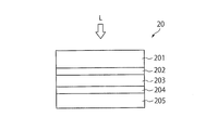
- FIG. 2 is a schematic configuration diagram of a solar cell 20 (photoelectric conversion element) according to the present embodiment.
- the solar cell 20 is an element having a function as a solar cell that converts light energy, such as sunlight L, incident on the cell into electric power.
- the solar cell 20 has a first graphene-containing film 202 between the transparent electrode 201 and the photoelectric conversion layer 203. Further, a second graphene-containing film 204 is provided between the counter electrode 205 and the photoelectric conversion layer 203.
- FIG. 2 shows an example having two graphene-containing films, but either one may be provided.
- the graphene-containing films 202 and 204 have specific anion permeability.
- This anion permeability can be evaluated by the following method.
- (I) Measurement comprising an aqueous solution containing an anion, a working electrode containing metallic silver, a counter electrode, and a reference electrode, wherein the working electrode, the counter electrode, and the reference electrode are electrically connected by an external circuit.
- some of the carbon atoms of the graphene skeleton included in the graphene-containing film may be replaced with nitrogen atoms.
- the nitrogen-substituted graphene-containing film has a large interaction with the anion, and can further reduce the diffusion of the anion. Further, the work function tends to be small, which is suitable for the cathode of the device.
- the doping amount of nitrogen atoms can be measured by an X-ray photoelectron spectrum (XPS), and is preferably 0.1 to 30 atom%, more preferably 1 to 10 atom%.
- a substituent containing an alkyl chain may be bonded to the graphene skeleton.
- dispersibility in an organic solvent is improved, film formation is easy, and ion diffusion can be reduced due to the substituent containing an alkyl chain. Therefore, the element life tends to be long.
- the electrode of the element may include silver.
- the electrode contains silver, the effect of ion diffusion can be more accurately predicted.
- a silver electrode is employed as the counter electrode 205, a silver thin film having an average thickness of 50 nm to 1 ⁇ m can be used.
- the silver thin film can be produced by vacuum evaporation, sputtering, or screen printing.
- an electrode containing silver can be used as the transparent electrode 201.
- a laminated film of a silver ultra-thin film and a conductive metal oxide or a silver nanowire can be used.
- Silver may be pure silver or an alloy.
- As the alloy an alloy with Pd, Pt, Au, Sn, Zn, and Cu is preferable.
- the silver nanowire preferably has an average diameter of 20 to 200 nm. If it is smaller than 20 nm, the stability tends to decrease. If it is larger than 200 nm, the transparency tends to decrease.
- the thickness of the ultrathin silver film and the diameter of the silver nanowire can be determined by the same method as described above.
- the conductive metal oxide film can be selected from any generally known one. Specifically, indium-doped tin oxide (Indium doped tin oxide, ITO), fluorine-doped tin oxide (Fluorine doped tin oxide, FTO), and aluminum-doped zinc oxide (Aluminium doped zinc oxide, AZO, etc.) are mentioned.
- the metal oxide has an amorphous structure, and preferably has a thickness of 30 to 200 nm, and the amorphous structure easily forms a continuous, uniform, and flat film. When it is larger than 200 nm, transparency tends to decrease, and it takes a long time to prepare, more preferably 35 to 100 nm, further preferably 40 to 70 nm. Is 0 Near for interaction with cations and anions is less preferred.
- the thickness of the ultra-thin silver film is preferably 2 to 20 nm. If it is smaller than 2 nm, the resistance tends to increase, and if it is larger than 20 nm, the transparency tends to decrease. More preferably, it is 3 to 15 nm, and further preferably, it is 5 to 10 nm.
- the photoelectric conversion device may further include an ultraviolet cut layer or a gas barrier layer.
- the UV absorber contained in the UV cut layer include 2-hydroxy-4-methoxybenzophenone, 2,2-dihydroxy-4-methoxybenzophenone, 2-hydroxy-4-methoxy-2-carboxybenzophenone, Benzophenone-based compounds such as hydroxy-4-n-octoxybenzophenone; 2- (2-hydroxy-3,5-ditert-butylphenyl) benzotriazole, 2- (2-hydroxy-5-methylphenyl) benzotriazole, Benzotriazole compounds such as 2- (2-hydroxy-5-tert-octylphenyl) benzotriazole; and salicylic acid ester compounds such as phenyl salicylate and p-octylphenyl salicylate. These are preferably those that cut off ultraviolet rays of 400 nm or less.
- the gas barrier layer a layer that blocks water vapor and oxygen is particularly preferable, and a layer that hardly transmits water vapor is particularly preferable.
- a layer made of an inorganic substance such as SiN, SiO 2 , SiC, SiO x N y , TiO 2 , and Al 2 O 3 , an ultra-thin glass, or the like can be preferably used.
- the thickness of the gas barrier layer is not particularly limited, but is preferably in the range of 0.01 to 3000 ⁇ m, and more preferably in the range of 0.1 to 100 ⁇ m. If the thickness is less than 0.01 ⁇ m, sufficient gas barrier properties tend not to be obtained.
- the water vapor transmission rate (moisture permeability) of the gas barrier layer is preferably from 10 2 g / m 2 ⁇ d to 10 -6 g / m 2 ⁇ d, more preferably from 10 1 g / m 2 ⁇ d to 10 -5 g. / m is 2 ⁇ d, more preferably 10 0 g / m 2 ⁇ d ⁇ 10 -4 g / m 2 ⁇ d.
- the moisture permeability can be measured based on JIS Z0208 and the like.
- a dry method is suitable.
- a vacuum evaporation method such as resistance heating evaporation, an electron beam evaporation, an induction heating evaporation, and an assist method using a plasma or an ion beam
- a reactive sputtering method such as a reactive sputtering method, and an ion beam.
- Sputtering method sputtering method such as ECR (Electron Cyclotron) sputtering method, physical vapor deposition method (PVD method) such as ion plating method, chemical vapor deposition method using heat, light, plasma, etc. (CVD method)
- PVD method physical vapor deposition method
- CVD method chemical vapor deposition method using heat, light, plasma, etc.
- an inorganic material such as glass, or an organic material such as PET, PEN, polycarbonate, or PMMA is used.
- an organic material such as PET, PEN, polycarbonate, or PMMA.
- the photoelectric conversion layer 203 is a semiconductor layer that converts light energy of incident light into electric power to generate a current.
- the photoelectric conversion layer 203 generally includes a p-type semiconductor layer and an n-type semiconductor layer.
- As the photoelectric conversion layer a laminate of a p-type polymer and an n-type material, a perovskite type represented by ABX 3 (where A is a monovalent cation, B is a divalent cation, and X is a halogen ion), silicon Semiconductors, inorganic compound semiconductors such as InGaAs, GaAs, chalcopyrite-based, CdTe-based, InP-based, and SiGe-based, quantum dot-containing type, and dye-sensitized type transparent semiconductors may be used. In any case, the efficiency is high, and the deterioration of the output can be further reduced.
- a buffer layer may be further inserted between the photoelectric conversion layer 203 and the transparent electrode 21 to promote or block charge injection.
- the counter electrode 205 is usually an opaque metal electrode, but the transparent electrode according to the embodiment may be used. Further, an ITO glass transparent electrode can be used as the counter electrode 205. In this case, the flexibility of the photoelectric conversion element is sacrificed, but light energy can be used with high efficiency. In addition, stainless steel, copper, titanium, nickel, chromium, tungsten, gold, silver, molybdenum, tin, zinc, or the like may be used as the metal electrode. In this case, the transparency tends to decrease.
- second graphene layer, a charge buffer layer, or a charge transport layer may be inserted between the counter electrode 205 and the photoelectric conversion layer 203.
- anode buffer layer and the charge transport layer for example, vanadium oxide, PEDOT / PSS, p-type polymer, vanadium pentoxide (V 2 O 5 ), 2,2 ′, 7,7′-Tetrakis [N, N-di (4-methoxyphenyl) amino] -9,9′-spirobifluorene (hereinafter referred to as Spiro-OMeTAD), nickel oxide (NiO), tungsten trioxide (WO 3 ), molybdenum trioxide (MoO 3 ), or the like is used. be able to.
- a metal oxide layer can be provided between the photoelectric conversion layer and the transparent electrode layer, particularly, adjacent to the graphene-containing film.
- a metal oxide layer include a brookite-type titanium oxide layer and a tin oxide layer. It is known that titanium oxide has three types of crystal structures, a rutile type, an anatase type, and a brookite type. In the embodiment, it is preferable to use a layer containing brookite-type titanium oxide.
- the brookite-type titanium oxide layer has an effect of suppressing the movement of halogen from the photoelectric conversion layer to the electrode and the movement of metal ions from the electrode to the photoelectric conversion layer. Therefore, the life of the electrodes and the electronic device can be extended.
- Such a brookite-type titanium oxide layer is preferably made of brookite-type titanium oxide nanoparticles, specifically, particles having an average particle diameter of 5 to 30 nm.
- the average particle size was measured by a particle size distribution measuring device.
- Such brookite-type nanoparticles are commercially available from, for example, High Purity Chemical Laboratory.
- the tin oxide layer can be formed by applying a solution obtained by dissolving tin chloride in n-butanol and heating under a high humidity condition.
- the photoelectric conversion element according to the embodiment may have a structure in which both surfaces are sandwiched between transparent electrodes.
- a solar cell having such a structure can efficiently use light from both sides.
- the energy conversion efficiency is generally 5% or more.
- the photoelectric conversion element of the present embodiment can be used as an optical sensor in addition to a photovoltaic cell and a solar cell.
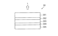
- FIG. 3 is a schematic configuration diagram of the organic EL element 30 (photoelectric conversion element) according to the present embodiment.
- the organic EL element 30 is an element having a function as a light emitting element that converts electric energy input to the element into light L.
- the organic EL element 30 has a first graphene-containing film 302 between the transparent electrode 301 and the photoelectric conversion layer 303. Further, a second graphene-containing film 304 is provided between the counter electrode 305 and the photoelectric conversion layer 303.
- FIG. 3 shows an example having two graphene-containing films, only one of them may be provided.
- the graphene-containing films 302 and 304 have specific anion permeability. This anion permeability can be evaluated by the same method as described above.
- the photoelectric conversion layer 303 is an organic thin film layer that recombines the charge injected from the transparent electrode 301 and the charge injected from the counter electrode 305 to convert electric energy into light.
- the photoelectric conversion layer 303 usually includes a p-type semiconductor layer and an n-type semiconductor layer.
- a buffer layer may be provided between the photoelectric conversion layer 303 and the counter electrode 305 to promote or block charge injection, and another buffer layer may be provided between the photoelectric conversion layer 303 and the transparent electrode 301.
- the counter electrode 35 is usually a metal electrode, but may be a transparent electrode.
- Examples of the material of the substrate of the element include resin materials such as polyethylene terephthalate (hereinafter, referred to as PET) and polyethylene naphthalate (hereinafter, referred to as PEN).
- the substrate is preferably one subjected to a flattening treatment.
- Example 1 After spin-coating an aqueous solution of graphene oxide manufactured by Graphenea on a layered structure of ITO (45 nm thick) / silver alloy (10 nm thick) / ITO (45 nm thick) on a PET film having a thickness of about 100 ⁇ m, and then hydration. The film is reduced at 120 ° C. in hydrazine vapor to produce a nitrogen-substituted graphene-containing film. From the XPS measurement, the content of nitrogen atoms to carbon atoms was 5%.
- a titanium wire is fixed on ITO / silver alloy / ITO with silver paste and electrically connected.
- the joint is protected with silicone tape, and the back of the PET film is also protected with silicone tape.
- This sample is immersed in a 3% by mass aqueous sodium chloride solution and subjected to cyclic voltammometry (sample area 0.85 cm 2 ).
- sample graphene-containing film was carried out only heating at 120 ° C., the sample treated at 120 ° C. with hydrazine hydrate in steam (0.61 cm 2), and spin coating graphene oxide Then, the sample (0.84 cm 2 ) treated at 120 ° C. is similarly subjected to cyclic voltammometry.
- FIG. 4 shows a cyclic voltammogram measured at 12.5 mV / s under the same measurement conditions. From the waveform area on the positive potential side, the reaction amount of chloride ions and silver, that is, the integrated charge amount can be obtained.
- the waveform area is the sum of the case of increasing the potential and the case of decreasing the potential. By comparing the waveform areas, the integrated charge amount can be compared.
- the accumulated charge of the sample (2) having no substituent graphene-containing film waveform area corresponding to the amount Q 0 is 7.8.
- Sample (3) treated at 120 ° C. in hydrated hydrazine vapor was 7.9, and sample (4) treated at 120 ° C. by spin coating with graphene oxide was 9.1.
- the amount of reaction with chloride ions in the graphene oxide film is larger than that without the graphene-containing film, which is considered to be due to the concentration effect.
- Example 2 A branched polyethyleneimine aqueous solution is added to an aqueous dispersion of graphene oxide, heated at 90 ° C. for 1 hour, hydrated hydrazine is added, and further heated at 90 ° C. for 1 hour. The resulting mixture is centrifuged at 12000 rpm to obtain a precipitate. The precipitate is redispersed in water and centrifuged at 12000 rpm to obtain a precipitate. This operation is performed twice to remove unreacted polyethyleneimine and hydrazine hydrate. The resulting precipitate is dried and then dispersed in isopropanol.
- the above isopropanol dispersion was applied on a layered structure of ITO / (thickness 45 nm) / silver alloy (thickness 10 nm) / ITO (thickness 45 nm) on a PET film having a thickness of about 100 ⁇ m with a bar coater and dried at 120 ° C. I do. From the XPS measurement, the content of nitrogen atoms to carbon atoms was 12%. In this case, there are many nitrogen atoms derived from polyethyleneimine. From the IR spectrum, an alkyl chain is bonded to graphene.
- a titanium wire is fixed on ITO / silver alloy / ITO with silver paste and electrically connected.
- an aqueous solution containing 3% by mass of sodium chloride is brought into contact.
- the aqueous solution is prevented from flowing out by a seal between the container containing the aqueous solution and the graphene-containing film.
- Perform cyclic voltammometry (sample area 12 cm 2 ).
- sample without a graphene-containing film cyclic voltammometry is similarly performed on a sample heated only at 130 ° C. All are measured under the same conditions (25 mV / s).
- the reaction amount of chloride ions and silver in the case where the graphene-containing film is present is less than 3% with respect to the case where the graphene-containing film is not present.
- Example 3 The surface of the Cu foil is heat-treated by laser irradiation, and the crystal grains are enlarged by annealing.
- This Cu foil was used as a base catalyst layer, and a single-layer nitrogen-substituted graphene graphene was formed by CVD using a mixed reaction gas of ammonia, methane, hydrogen, and argon (15: 60: 65: 200 ccm) at 1000 ° C. for 5 minutes. Produce a containing film. At this time, although a single-layer nitrogen-substituted graphene-containing film is almost formed, two or more nitrogen-substituted graphene-containing films are partially formed depending on conditions. Further, after treatment at 1000 ° C.
- the mixture is cooled in a mixed gas stream of argon.
- the thermal transfer film 150 ⁇ m thick
- the single-layer nitrogen-substituted graphene-containing film are pressed, they are immersed in ammonia-alkali cupric chloride etchant to dissolve Cu, and the single-layer nitrogen-substituted graphene-containing film is transferred onto the thermal transfer film. I do.
- the same operation is repeated four times to obtain a multilayer nitrogen-substituted graphene-containing film.
- a titanium wire is fixed on ITO / silver alloy / ITO with silver paste and electrically connected.
- an aqueous solution containing 3% by mass of sodium chloride is brought into contact.
- the aqueous solution is prevented from flowing out by a seal between the container containing the aqueous solution and the graphene-containing film.
- Perform cyclic voltammometry (sample area 12 cm 2 ).
- a sample without a graphene-containing film a sample subjected to only heating at 100 ° C. is similarly subjected to cyclic voltammometry. All are measured under the same conditions (25 mV / s).
- the reaction amount of chloride ions and silver in the case where the graphene-containing film is present is less than 1% with respect to the case where the graphene-containing film is not present.
- Example 4 The graphene isopropanol dispersion obtained in Example 2 was applied on a silver nanowire coating film having an average diameter of 40 nm formed on a PET film having a thickness of about 100 ⁇ m with a bar coater, and the concentration of sodium chloride was 1% by mass. Except for the above, the chloride ion permeability was evaluated in the same manner as in Example 2. All are measured under the same conditions (25 mV / s). As a result, the reaction amount between chloride ions and silver in the case where the graphene-containing film is present is less than 4% with respect to the case where the graphene-containing film is not present.
- Example 5 The solar cell 50 shown in FIG. 5 is created.
- graphene oxide graphene oxide manufactured by Graphenea was formed on a laminated structure 502 of ITO (45 nm thick) / silver alloy (10 nm thick) / ITO (45 nm thick) on a PET film 501 having a thickness of about 100 ⁇ m. After spin-coating the aqueous solution, it is reduced at 120 ° C. in hydrated hydrazine vapor to form a nitrogen-substituted graphene-containing film 503. From the XPS measurement, the content of nitrogen atoms to carbon atoms was 5%. A toluene solution of C 60 -PCBM is applied on the 503 as an electron transport layer 504 by a bar coater and dried.
- a chlorobenzene solution containing poly (3-hexylthiophene-2,5-diyl) (hereinafter, referred to as P3HT) and C 60 -PCBM is applied with a bar coater, and dried at 100 ° C. for 20 minutes to obtain a photoelectric conversion layer 505. Is prepared.
- the surface of the adhesive layer 508 is bonded onto the photoelectric conversion layer 505.
- a UV cut ink containing 2-hydroxy-4-methoxybenzophenone is screen-printed on the PET surface to form a UV cut layer 509.
- a silica film is formed on the ultraviolet cut layer by a vacuum evaporation method to form a gas barrier layer 511, and a solar cell 50 is formed.
- the obtained solar cell has an energy conversion efficiency of 5% or more with respect to 1 SUN of sunlight, and the deterioration of the efficiency is less than 5% even when left outdoors for one month.
- Example 6 As in Example 2, an aqueous solution of branched polyethyleneimine is added to an aqueous dispersion of graphene oxide, heated at 90 ° C. for 1 hour, and hydrated hydrazine is added, followed by heating at 90 ° C. for 1 hour. The resulting mixture is centrifuged at 12000 rpm to obtain a precipitate. The precipitate is redispersed in water and centrifuged at 12000 rpm to obtain a precipitate. This operation is performed twice to remove unreacted polyethyleneimine and hydrazine hydrate. The resulting precipitate is dried and then dispersed in isopropanol.
- the above isopropanol dispersion is applied on a laminated structure of ITO (thickness 45 nm) / silver alloy (thickness 10 nm) / ITO (thickness 45 nm) on a PET film having a thickness of about 100 ⁇ m with a bar coater and dried at 120 ° C.
- a nitrogen-substituted graphene-containing film From the XPS measurement, the content of nitrogen atoms to carbon atoms was 12%. In this case, there are many nitrogen atoms derived from polyethyleneimine. From the IR spectrum, an alkyl chain is bonded to graphene.
- a toluene solution of C 60 -PCBM is applied as an electron transport layer on the graphene-containing film using a bar coater and dried.
- a chlorobenzene solution containing poly (3-hexylthiophene-2,5-diyl) (hereinafter, referred to as P3HT) and C 60 -PCBM is applied with a bar coater and dried at 100 ° C. for 20 minutes to form a photoelectric conversion layer. Make it.
- the surface of the stainless steel foil with the insulating ceramic film formed on the opposite surface is treated with dilute hydrochloric acid to remove the surface oxide film, and then spin-coated with the above-mentioned isopropanol dispersion of nitrogen-substituted graphene to obtain a nitrogen-substituted graphene-containing film.
- a solar cell is manufactured in the same manner as in Example 5.
- the obtained solar cell shows an energy conversion efficiency of 5% or more with respect to 1 SUN of sunlight, and the deterioration of the efficiency is less than 2% even when left outdoors for one month.
- Example 1 A solar cell is manufactured in the same manner as in Example 5, except that the nitrogen-substituted graphene-containing films 503 and 507 are not manufactured.
- the obtained solar cell exhibits an energy conversion efficiency of 5% or more with respect to 1 SUN of sunlight, but the efficiency is reduced to 80% or more when left outdoors for one month.
- Example 7 The organic EL element 60 shown in FIG. 6 is created.
- graphene oxide manufactured by Graphenea Co., Ltd. was formed on a laminated structure 602 of ITO (45 nm thick) / silver alloy (10 nm thick) / ITO (45 nm thick) on a PET film (thickness of about 100 ⁇ m) 601. Is spin-coated with an aqueous solution of the above, and reduced at 120 ° C. in hydrated hydrazine vapor to form a nitrogen-substituted graphene-containing film 603. From the XPS measurement, the content of nitrogen atoms to carbon atoms was 5%.
- a photoelectric conversion layer 604 is formed by depositing tris (8-hydroxyquinoline) aluminum (Alq 3 ) (40 nm) over the nitrogen-substituted graphene-containing film 603.
- N, N'-di-1-naphthyl-N, N'-diphenyl-1,1'-biphenyl-4,4'-diamine (hereinafter referred to as NPD) is deposited thereon to a thickness of 30 nm and transported by holes.
- the layer 605 is formed.
- a gold electrode 606 is formed thereon by sputtering. Further, an organic EL element is manufactured by sealing the periphery.
- the obtained organic EL device has little deterioration of the output light, and the decrease in output is 5% or less even after 1000 hours of continuous operation.
- Example 1 an aqueous solution of graphene oxide manufactured by Graphenea was formed on a laminated structure of ITO (thickness: 45 nm) / silver alloy (thickness: 10 nm) / ITO (thickness: 45 nm) on a PET film having a thickness of about 100 ⁇ m. Is spin-coated and reduced at 120 ° C. in hydrated hydrazine vapor to produce a nitrogen-substituted graphene-containing film. From the XPS measurement, the content of nitrogen atoms to carbon atoms was 5%.
- a photoelectric conversion layer is formed by depositing tris (8-hydroxyquinoline) aluminum (Alq 3 ) (40 nm) as a light-emitting layer on graphene.
- N, N'-di-1-naphthyl-N, N'-diphenyl-1,1'-biphenyl-4,4'-diamine (hereinafter referred to as NPD) is deposited thereon to a thickness of 30 nm and transported by holes.
- NPD N, N'-di-1-naphthyl-N, N'-diphenyl-1,1'-biphenyl-4,4'-diamine
- An a-ITO (40 nm) / silver (10 nm) / a-ITO film (50 nm) is formed thereon by a sputtering method.
- an organic EL element is manufactured by sealing the outer periphery of the element.
- the obtained organic EL element has little deterioration of the output light, and the output reduction is 6% or less even after 1000 hours of continuous operation.
- Comparative Example 2 An organic EL device is manufactured in the same manner as in Example 7, except that the nitrogen-containing graphene-containing layer is not formed. When the obtained organic EL device is continuously operated for 1000 hours, the output is reduced to 80% or less.
- Example 9 After spin-coating an aqueous solution of graphene oxide manufactured by Graphenea on a layered structure of ITO (45 nm thick) / silver alloy (10 nm thick) / ITO (45 nm thick) on a PET film having a thickness of about 100 ⁇ m, and then hydration. The film is reduced at 80 ° C. in hydrazine vapor to produce a nitrogen-substituted graphene-containing film. From the XPS measurement, the content of nitrogen atoms to carbon atoms was 3%.
- an organic EL device is manufactured in the same manner as in Example 8.
- the obtained organic EL element has little deterioration of the output light, and the output reduction is 10% or less even after 1000 hours of continuous operation.
- an organic EL device is manufactured in the same manner as in Example 8.
- the output is reduced to 50% or less.
- Example 10 As in Example 2, an aqueous solution of branched polyethyleneimine is added to an aqueous dispersion of graphene oxide, heated at 90 ° C. for 1 hour, and hydrated hydrazine is added, followed by heating at 90 ° C. for 1 hour. The resulting mixture is centrifuged at 12000 rpm to obtain a precipitate. The precipitate is redispersed in water and centrifuged at 12000 rpm to obtain a precipitate. This operation is performed twice to remove unreacted polyethyleneimine and hydrazine hydrate. The resulting precipitate is dried and then dispersed in isopropanol.
- a silver nanowire having a diameter of 40 nm is coated on a PET film having a thickness of about 100 ⁇ m with a bar coater, and the isopropanol dispersion is coated thereon with a bar coater and dried at 120 ° C. to obtain a nitrogen-substituted graphene-containing film.
- the content of nitrogen atoms to carbon atoms is 12%. In this case, there are many nitrogen atoms derived from polyethyleneimine. From the IR spectrum, the alkyl chain is bonded to graphene.
- a toluene solution of C 60 -PCBM is applied as an electron transport layer on the graphene-containing film using a bar coater and dried.
- a chlorobenzene solution containing poly (3-hexylthiophene-2,5-diyl) (hereinafter, referred to as P3HT) and C60-PCBM is applied with a bar coater, and dried at 100 ° C. for 20 minutes to form a photoelectric conversion layer. I do.
- the surface of the stainless steel foil with the insulating ceramic film formed on the opposite surface is treated with dilute hydrochloric acid to remove the surface oxide film, and then spin-coated with the above-mentioned isopropanol dispersion of nitrogen-substituted graphene to obtain a nitrogen-substituted graphene-containing film.
- a solar cell is manufactured in the same manner as in Example 5.
- the obtained solar cell shows an energy conversion efficiency of 5% or more with respect to 1 SUN of sunlight, and the deterioration of the efficiency is less than 3% even when left outdoors for one month.
Landscapes
- Physics & Mathematics (AREA)
- Electromagnetism (AREA)
- Microelectronics & Electronic Packaging (AREA)
- General Physics & Mathematics (AREA)
- Engineering & Computer Science (AREA)
- Computer Hardware Design (AREA)
- Condensed Matter Physics & Semiconductors (AREA)
- Power Engineering (AREA)
- Optics & Photonics (AREA)
- Photovoltaic Devices (AREA)
- Electroluminescent Light Sources (AREA)
- Carbon And Carbon Compounds (AREA)
- Hybrid Cells (AREA)
Abstract
Le problème décrit par la présente invention est de fournir un procédé d'évaluation simple de la perméabilité aux anions d'un film contenant du graphène et un élément de conversion photoélectrique utilisant un film contenant du graphène présentant une perméabilité ionique contrôlée. La solution de l'invention porte sur un procédé d'évaluation de la perméabilité aux anions d'un film contenant du graphène dans lequel (i) un dispositif de mesure est préparé, le dispositif de mesure comprenant une solution aqueuse comprenant des anions, une électrode de travail comprenant de l'argent métallique, une contre-électrode et une électrode de référence, (ii) le potentiel d'électrode de l'électrode de travail par rapport à la contre-électrode lorsque les électrodes sont mises en contact avec la solution aqueuse est périodiquement modifiée par une méthode de balayage, et le courant de réaction I0 entre l'argent métallique et les anions est mesuré, (iii) le courant de réaction I1 lorsqu'un film contenant du graphène connecté électriquement à l'électrode de travail est mis en contact avec la solution aqueuse au lieu de l'électrode de travail est mesuré, et (iv) la perméabilité aux anions du film contenant du graphène est évaluée par la comparaison d'I0 et d'I1. Ainsi, l'invention concerne un élément de conversion photoélectrique comprenant un film contenant du graphène selon lequel, lorsque le film contenant du graphène est utilisé pour mesurer le courant de réaction conformément au procédé précité, la courbe du courant de réaction I1 présente un pic sur le côté potentiel positif, et la charge intégrée Q1 sur le côté potentiel positif est inférieure ou égale à 20 % de la charge intégrée Q0 sur le côté positif sans film contenant du graphène.
Priority Applications (6)
| Application Number | Priority Date | Filing Date | Title |
|---|---|---|---|
| EP18933023.6A EP3851844A4 (fr) | 2018-09-13 | 2018-09-13 | Procédé d'évaluation de la perméabilité aux anions d'un film contenant du graphène et élément de conversion photoélectrique |
| PCT/JP2018/033968 WO2020054018A1 (fr) | 2018-09-13 | 2018-09-13 | Procédé d'évaluation de la perméabilité aux anions d'un film contenant du graphène et élément de conversion photoélectrique |
| CN201880056118.2A CN111183357B (zh) | 2018-09-13 | 2018-09-13 | 含石墨烯膜的阴离子透过性评价方法和光电转换元件 |
| JP2020512068A JP7022200B2 (ja) | 2018-09-13 | 2018-09-13 | グラフェン含有膜の陰イオン透過性評価方法および光電変換素子 |
| US16/818,112 US11217714B2 (en) | 2018-09-13 | 2020-03-13 | Evaluation method on anion permeability of graphene-containing membrane and photoelectric conversion device |
| US17/456,748 US11682740B2 (en) | 2018-09-13 | 2021-11-29 | Evaluation method on anion permeability of graphene-containing membrane and photoelectric conversion device |
Applications Claiming Priority (1)
| Application Number | Priority Date | Filing Date | Title |
|---|---|---|---|
| PCT/JP2018/033968 WO2020054018A1 (fr) | 2018-09-13 | 2018-09-13 | Procédé d'évaluation de la perméabilité aux anions d'un film contenant du graphène et élément de conversion photoélectrique |
Related Child Applications (1)
| Application Number | Title | Priority Date | Filing Date |
|---|---|---|---|
| US16/818,112 Continuation US11217714B2 (en) | 2018-09-13 | 2020-03-13 | Evaluation method on anion permeability of graphene-containing membrane and photoelectric conversion device |
Publications (1)
| Publication Number | Publication Date |
|---|---|
| WO2020054018A1 true WO2020054018A1 (fr) | 2020-03-19 |
Family
ID=69776680
Family Applications (1)
| Application Number | Title | Priority Date | Filing Date |
|---|---|---|---|
| PCT/JP2018/033968 WO2020054018A1 (fr) | 2018-09-13 | 2018-09-13 | Procédé d'évaluation de la perméabilité aux anions d'un film contenant du graphène et élément de conversion photoélectrique |
Country Status (5)
| Country | Link |
|---|---|
| US (2) | US11217714B2 (fr) |
| EP (1) | EP3851844A4 (fr) |
| JP (1) | JP7022200B2 (fr) |
| CN (1) | CN111183357B (fr) |
| WO (1) | WO2020054018A1 (fr) |
Cited By (2)
| Publication number | Priority date | Publication date | Assignee | Title |
|---|---|---|---|---|
| JP2021193386A (ja) * | 2018-09-13 | 2021-12-23 | 株式会社東芝 | 電気化学素子 |
| JPWO2022029862A1 (fr) * | 2020-08-04 | 2022-02-10 |
Families Citing this family (1)
| Publication number | Priority date | Publication date | Assignee | Title |
|---|---|---|---|---|
| CN115369439A (zh) * | 2022-04-11 | 2022-11-22 | 天津工业大学 | 耦合太阳能光热的自支撑析氧电催化剂及制备方法与应用 |
Citations (6)
| Publication number | Priority date | Publication date | Assignee | Title |
|---|---|---|---|---|
| US4818365A (en) * | 1986-10-14 | 1989-04-04 | Monsanto Company | Solid state indicator electrode and method of making same |
| JPH09283866A (ja) | 1996-04-10 | 1997-10-31 | Nippon Sheet Glass Co Ltd | 透明導電膜付き基板 |
| US20140174954A1 (en) * | 2012-10-19 | 2014-06-26 | Prieto Battery, Inc. | Detection of defects in solid-polymer coatings using reduction-oxidation probes |
| WO2014188166A1 (fr) * | 2013-05-20 | 2014-11-27 | Isis Innovation Limited | Détermination électrochimique de la concentration d'un halogénure ou d'un pseudohalogénure |
| JP2016086173A (ja) * | 2014-10-28 | 2016-05-19 | 株式会社半導体エネルギー研究所 | 発光素子、発光装置、電子機器及び照明装置 |
| JP2017135379A (ja) * | 2016-01-21 | 2017-08-03 | 株式会社東芝 | 透明電極、電子デバイス、および電子デバイスの製造方法 |
Family Cites Families (8)
| Publication number | Priority date | Publication date | Assignee | Title |
|---|---|---|---|---|
| JPH0331753A (ja) | 1989-06-29 | 1991-02-12 | Nippon Filcon Co Ltd | 生体液中の塩素イオンの濃度を測定する方法 |
| ES2768330T3 (es) * | 2010-10-15 | 2020-06-22 | Evoqua Water Tech Llc | Membranas de intercambio aniónico y proceso para su producción |
| JP5566935B2 (ja) * | 2011-03-25 | 2014-08-06 | 株式会社東芝 | 発光装置 |
| JP6130757B2 (ja) * | 2013-09-04 | 2017-05-17 | 本田技研工業株式会社 | 光電変換材料及びその製造方法と、それを用いた有機薄膜太陽電池 |
| EP3207576A4 (fr) * | 2015-01-16 | 2017-10-25 | SABIC Global Technologies B.V. | Activation de surface d'un polymère organique et réduction de nanoparticules en mode monotope |
| US20170144107A1 (en) * | 2015-11-24 | 2017-05-25 | National University Of Singapore | Graphene-based membrane and method of preparation thereof |
| CN107037085B (zh) * | 2016-11-24 | 2019-06-07 | 黑龙江大学 | 还原氧化石墨烯-聚乙烯亚胺-四氧化三钴氧化物半导体复合材料及制备方法和应用 |
| JP6944427B2 (ja) * | 2018-09-13 | 2021-10-06 | 株式会社東芝 | 膜状構造体の陰イオン透過性評価方法および電気化学素子 |
-
2018
- 2018-09-13 JP JP2020512068A patent/JP7022200B2/ja active Active
- 2018-09-13 EP EP18933023.6A patent/EP3851844A4/fr active Pending
- 2018-09-13 WO PCT/JP2018/033968 patent/WO2020054018A1/fr unknown
- 2018-09-13 CN CN201880056118.2A patent/CN111183357B/zh active Active
-
2020
- 2020-03-13 US US16/818,112 patent/US11217714B2/en active Active
-
2021
- 2021-11-29 US US17/456,748 patent/US11682740B2/en active Active
Patent Citations (6)
| Publication number | Priority date | Publication date | Assignee | Title |
|---|---|---|---|---|
| US4818365A (en) * | 1986-10-14 | 1989-04-04 | Monsanto Company | Solid state indicator electrode and method of making same |
| JPH09283866A (ja) | 1996-04-10 | 1997-10-31 | Nippon Sheet Glass Co Ltd | 透明導電膜付き基板 |
| US20140174954A1 (en) * | 2012-10-19 | 2014-06-26 | Prieto Battery, Inc. | Detection of defects in solid-polymer coatings using reduction-oxidation probes |
| WO2014188166A1 (fr) * | 2013-05-20 | 2014-11-27 | Isis Innovation Limited | Détermination électrochimique de la concentration d'un halogénure ou d'un pseudohalogénure |
| JP2016086173A (ja) * | 2014-10-28 | 2016-05-19 | 株式会社半導体エネルギー研究所 | 発光素子、発光装置、電子機器及び照明装置 |
| JP2017135379A (ja) * | 2016-01-21 | 2017-08-03 | 株式会社東芝 | 透明電極、電子デバイス、および電子デバイスの製造方法 |
Non-Patent Citations (1)
| Title |
|---|
| See also references of EP3851844A4 |
Cited By (6)
| Publication number | Priority date | Publication date | Assignee | Title |
|---|---|---|---|---|
| JP2021193386A (ja) * | 2018-09-13 | 2021-12-23 | 株式会社東芝 | 電気化学素子 |
| JP7263458B2 (ja) | 2018-09-13 | 2023-04-24 | 株式会社東芝 | 燃料電池 |
| JPWO2022029862A1 (fr) * | 2020-08-04 | 2022-02-10 | ||
| WO2022029862A1 (fr) * | 2020-08-04 | 2022-02-10 | 株式会社 東芝 | Procédé d'évaluation d'électrode |
| US20220170871A1 (en) * | 2020-08-04 | 2022-06-02 | Kabushiki Kaisha Toshiba | Electrode evaluation method |
| JP7198389B2 (ja) | 2020-08-04 | 2022-12-28 | 株式会社東芝 | 電極評価方法 |
Also Published As
| Publication number | Publication date |
|---|---|
| EP3851844A1 (fr) | 2021-07-21 |
| CN111183357A (zh) | 2020-05-19 |
| JPWO2020054018A1 (ja) | 2020-12-17 |
| CN111183357B (zh) | 2022-09-02 |
| JP7022200B2 (ja) | 2022-02-17 |
| US20200212231A1 (en) | 2020-07-02 |
| US11682740B2 (en) | 2023-06-20 |
| US20220085221A1 (en) | 2022-03-17 |
| US11217714B2 (en) | 2022-01-04 |
| EP3851844A4 (fr) | 2022-04-20 |
Similar Documents
| Publication | Publication Date | Title |
|---|---|---|
| JP7048785B2 (ja) | 透明電極、およびその製造方法、ならびにその透明電極を用いた電子デバイス | |
| JP6697406B2 (ja) | 透明電極、電子デバイス、および電子デバイスの製造方法 | |
| US11682740B2 (en) | Evaluation method on anion permeability of graphene-containing membrane and photoelectric conversion device | |
| Foo et al. | Recent review on electron transport layers in perovskite solar cells | |
| KR20240006091A (ko) | 페로브스카이트 물질 디바이스에서의 이중- 및 삼중-층 계면 층 | |
| US11387375B2 (en) | Graphene-containing membrane, process for producing the same, graphene-containing membrane laminate and photoelectric conversion device | |
| US20220181569A1 (en) | Transparent electrode, method of producing transparent electrode, and electronic device | |
| Chen et al. | Wo 3 nanoparticles or nanorods incorporating Cs 2 Co 3/PCBM buffer bilayer as carriers transporting materials for perovskite solar cells | |
| JP6782211B2 (ja) | 透明電極、それを用いた素子、および素子の製造方法 | |
| US11942575B2 (en) | Transparent electrode, method of producing transparent electrode, and electronic device | |
| US20230025098A1 (en) | Transparent electrode, method for producing the same, and electronic device using transparent electrode | |
| WO2022185485A1 (fr) | Électrode transparente, son procédé de production, et dispositif électronique utilisant une électrode transparente | |
| US20240138164A1 (en) | Multilayer Back Contacts for Perovskite Photovoltaic Devices |
Legal Events
| Date | Code | Title | Description |
|---|---|---|---|
| ENP | Entry into the national phase |
Ref document number: 2020512068 Country of ref document: JP Kind code of ref document: A |
|
| 121 | Ep: the epo has been informed by wipo that ep was designated in this application |
Ref document number: 18933023 Country of ref document: EP Kind code of ref document: A1 |
|
| NENP | Non-entry into the national phase |
Ref country code: DE |
|
| ENP | Entry into the national phase |
Ref document number: 2018933023 Country of ref document: EP Effective date: 20210413 |