WO2020050158A1 - 電子部品ユニット - Google Patents
電子部品ユニット Download PDFInfo
- Publication number
- WO2020050158A1 WO2020050158A1 PCT/JP2019/034069 JP2019034069W WO2020050158A1 WO 2020050158 A1 WO2020050158 A1 WO 2020050158A1 JP 2019034069 W JP2019034069 W JP 2019034069W WO 2020050158 A1 WO2020050158 A1 WO 2020050158A1
- Authority
- WO
- WIPO (PCT)
- Prior art keywords
- housing
- relay
- substrate
- contact
- connector
- Prior art date
- Legal status (The legal status is an assumption and is not a legal conclusion. Google has not performed a legal analysis and makes no representation as to the accuracy of the status listed.)
- Ceased
Links
Images






Classifications
-
- A—HUMAN NECESSITIES
- A61—MEDICAL OR VETERINARY SCIENCE; HYGIENE
- A61B—DIAGNOSIS; SURGERY; IDENTIFICATION
- A61B1/00—Instruments for performing medical examinations of the interior of cavities or tubes of the body by visual or photographical inspection, e.g. endoscopes; Illuminating arrangements therefor
- A61B1/00112—Connection or coupling means
- A61B1/00114—Electrical cables in or with an endoscope
-
- H—ELECTRICITY
- H01—ELECTRIC ELEMENTS
- H01R—ELECTRICALLY-CONDUCTIVE CONNECTIONS; STRUCTURAL ASSOCIATIONS OF A PLURALITY OF MUTUALLY-INSULATED ELECTRICAL CONNECTING ELEMENTS; COUPLING DEVICES; CURRENT COLLECTORS
- H01R12/00—Structural associations of a plurality of mutually-insulated electrical connecting elements, specially adapted for printed circuits, e.g. printed circuit boards [PCB], flat or ribbon cables, or like generally planar structures, e.g. terminal strips, terminal blocks; Coupling devices specially adapted for printed circuits, flat or ribbon cables, or like generally planar structures; Terminals specially adapted for contact with, or insertion into, printed circuits, flat or ribbon cables, or like generally planar structures
- H01R12/50—Fixed connections
- H01R12/51—Fixed connections for rigid printed circuits or like structures
- H01R12/52—Fixed connections for rigid printed circuits or like structures connecting to other rigid printed circuits or like structures
-
- H—ELECTRICITY
- H04—ELECTRIC COMMUNICATION TECHNIQUE
- H04N—PICTORIAL COMMUNICATION, e.g. TELEVISION
- H04N23/00—Cameras or camera modules comprising electronic image sensors; Control thereof
- H04N23/50—Constructional details
- H04N23/51—Housings
-
- H—ELECTRICITY
- H04—ELECTRIC COMMUNICATION TECHNIQUE
- H04N—PICTORIAL COMMUNICATION, e.g. TELEVISION
- H04N25/00—Circuitry of solid-state image sensors [SSIS]; Control thereof
-
- G—PHYSICS
- G02—OPTICS
- G02B—OPTICAL ELEMENTS, SYSTEMS OR APPARATUS
- G02B23/00—Telescopes, e.g. binoculars; Periscopes; Instruments for viewing the inside of hollow bodies; Viewfinders; Optical aiming or sighting devices
- G02B23/24—Instruments or systems for viewing the inside of hollow bodies, e.g. fibrescopes
- G02B23/2476—Non-optical details, e.g. housings, mountings, supports
- G02B23/2484—Arrangements in relation to a camera or imaging device
-
- H—ELECTRICITY
- H04—ELECTRIC COMMUNICATION TECHNIQUE
- H04N—PICTORIAL COMMUNICATION, e.g. TELEVISION
- H04N23/00—Cameras or camera modules comprising electronic image sensors; Control thereof
- H04N23/50—Constructional details
- H04N23/555—Constructional details for picking-up images in sites, inaccessible due to their dimensions or hazardous conditions, e.g. endoscopes or borescopes
Definitions
- the present invention relates to an electronic component unit.
- Priority is claimed on Japanese Patent Application No. 2018-167119, filed Sep. 6, 2018, the content of which is incorporated herein by reference.
- an imaging module having a configuration in which a solid-state imaging device (hereinafter, also simply referred to as an imaging device) is electrically connected to a distal end of an electric cable via a wiring board is often used (for example, Patent Document 1).
- the ends of a plurality of electric cables are electrically connected to the wiring of the wiring board, and each electric cable is electrically connected to the imaging element by the wiring of the wiring board.
- a step of passing the imaging module through a thin resin tube is performed. After this step, it is common practice to solder the opposite end (rear end) of each electric cable to a relay board electrically connected to a video processing display device including a monitor.
- the step of passing the imaging module through the resin tube may be performed by inserting the imaging module into the tube from the imaging element side, or by inserting the imaging module at the rear end (proximal end, specifically, the rear end of the electric cable). It is also widely used to insert the tube into the tube. For example, when an electrical connection plug that is detachably fitted to the receptacle on the video processing display device side is assembled at the rear end of the imaging module, it is difficult to insert the imaging module through the tube from the rear end side. For this reason, in the step of passing the imaging module through the tube from the rear end, the rear end of the electric cable of the imaging module is inserted into the tube with the cable end without the plug.
- the problem to be solved by the aspects of the present invention is that electrical connection between an electronic module such as an imaging module and other devices can be easily performed without using a receptacle and a plug that is inserted and fitted into the receptacle. It is to provide an electronic component unit.
- An electronic component unit includes an electronic module in which a rear substrate is electrically connected to any one of an imaging element, a laser element, and a sensor element via an electric cable; An external connection terminal electrically connected to a circuit, a relay substrate including a terminal connection electrode in which the external connection terminal is directly or electrically connected via a connection conductor, and an external connection terminal attached to the relay substrate; A relay connector for electrically connecting an electrode formed on the rear substrate of the electronic module to a relay conductor electrically connected to the terminal connection electrode via a wiring formed on the relay substrate.
- the relay unit connector the connector base member attached to the relay board, the relay conductor provided on the connector base member, the electronic module Sandwiching the serial rear substrate between said connector base member, and a pressing member for pressing the electrodes of the rear substrate in the contact portion of the relay conductor.
- the electronic component unit further includes an external connection connector attached to the relay substrate, wherein the external connection connector includes a terminal support provided with the external connection terminal, and the relay substrate mounted on the relay substrate.
- a housing cylinder mounted in a protruding state from the outer periphery of the substrate and housing the terminal support, wherein the external connection terminal has a surface facing a mating contact insertion space secured in the housing cylinder of the terminal support.
- a base end of the external connection terminal provided on the relay substrate and located on the relay substrate side may be electrically connected to the terminal connection electrode of the relay substrate.
- the electronic component unit described above has the external connection terminal to which an electric wire is electrically connected, and a connector housing that houses the external connection terminal and is assembled around the relay board and the relay connector.
- the connection terminal may be electrically connected to the terminal connection electrode of the relay board via the connection conductor including the electric wire.
- the connector base member has a substrate supporting surface with which the rear substrate abuts, and the pressing member engages with the connector base member with an engaging portion that engages with the connector base member.
- a holding portion that holds the rear substrate against the substrate support surface in the state where the substrate is held.
- an electronic module such as an imaging module
- another apparatus for example, electrical connection of an electronic module, such as an imaging module, and another apparatus (relay board), without using a receptacle and the plug inserted and fitted in a receptacle.
- the electronic module and the relay conductor are formed by simply pressing the rear substrate of the electronic module against the contact portion of the relay conductor of the relay connector by the pressing member of the relay connector. Electrical connection can be easily realized. As a result, electrical connection between the electronic module and the relay board can be easily realized via the relay conductor of the relay connector.
- the electronic component unit for example, by adopting a rear substrate of the electronic module having a size that can be inserted into a tube that houses the electronic element and the electric cable, It is possible to use a tube having a diameter as small as possible within a range in which the electronic element can be accommodated.
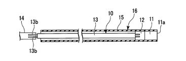
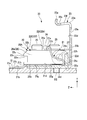
- FIG. 2 is a cross-sectional view illustrating a configuration of an imaging module of the electronic endoscope system in FIG. 1.
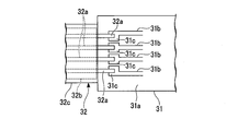
- FIG. 2 is a plan view showing the vicinity of a terminal connection electrode of a relay board to which an external connection terminal of an external connection connector of the electronic component unit (imaging unit) of FIG. 1 is electrically connected.
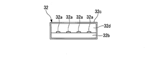
- FIG. 2 is a diagram illustrating a configuration of an external connector of the electronic component unit (imaging unit) of FIG. 1 as viewed from a front end (a protruding end with respect to a relay board).
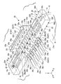
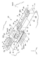
- FIG. 2 is a perspective view illustrating a relay connector of a relay unit of the electronic component unit in FIG. 1, showing a state in which a holding member is opened with respect to a housing.
- FIG. 6 is a perspective view showing a state in which the rear board of the electronic module is clamped and fixed between the housing and the holding member which is closed with respect to the housing and is in the closed maintenance locking state with respect to the relay connector of FIG. 5.
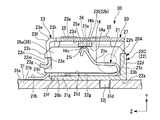
- FIG. 6 is a cross-sectional view showing the vicinity of a contact accommodating groove of the relay connector of FIG. 5.
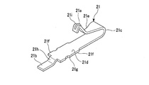
- FIG. 7 is a transverse sectional view showing the vicinity of a contact receiving groove of the relay connector of FIG. 6. It is a perspective view which shows the contact of the relay part connector of FIG. FIG.
- FIG. 2 is a diagram illustrating a first main surface of a rear substrate of an imaging module of the electronic component unit (imaging unit) in FIG. 1.
- FIG. 11 is a diagram illustrating a connection state of a conductor of a coaxial cable of an electric cable of an imaging module to a conductor connection terminal of a rear substrate of FIG. 10.
- FIG. 3 is a perspective view illustrating the vicinity of an image sensor of the image sensor module. It is sectional drawing which shows the front end part vicinity of the back side board of an imaging module. It is a figure showing the neighborhood of a relay unit before assembling of a substrate accommodation housing of an electronic parts unit of a 2nd embodiment.
- FIG. 15 is a diagram illustrating an example of the board housing housing and the external connection connector assembled to the electronic component unit in FIG.
- FIG. 14 illustrates a structure of the external connection connector as viewed from a front end (insertion end) thereof.
- FIG. 15 is a diagram illustrating an example of the board housing housing and the external connection connector assembled in the electronic component unit in FIG. 14, and illustrates a structure of the external connection connector as viewed from a side. It is a perspective view showing a modification of a relay connector, and shows a state where a control member was opened to a housing.
- 16 is a perspective view showing a state in which a connection end substrate (a rear substrate of an imaging module) is sandwiched between a holding member and a housing which are closed with respect to a housing and are kept in a closed maintenance locking state with respect to the relay connector of FIG. 16. It is.
- FIG. 16 is a perspective view showing a state in which a connection end substrate (a rear substrate of an imaging module) is sandwiched between a holding member and a housing which are closed with respect to a housing and are kept in a closed maintenance locking state with respect to the relay connector of
- FIG. 17 is a transverse cross-sectional view showing the vicinity of a contact receiving groove of the relay connector of FIG. 16.
- FIG. 17 is an enlarged front sectional view showing the vicinity of a positioning pin and an erroneous insertion prevention protruding wall of the relay connector of FIG. 16.
- the electronic component unit U1 shown in FIG. 1 is an imaging unit that can be used as a part of the videoscope device of the electronic endoscope system 50.
- the electronic component unit U1 includes an imaging module 10 which is an electronic module including an imaging element 11 (electronic element), and a relay unit 30 for electrically connecting an electric circuit of the imaging module 10 to an external circuit. Having.
- the imaging module 10 includes an imaging element 11 (electronic element), a wiring board 12 on which the imaging element 11 is mounted (hereinafter, also referred to as a head-side substrate), and a head-side substrate 12.
- An electric cable 13 electrically connected to the image sensor 11 via a wiring (not shown) and a rear end electrically connected to a front end of the electric cable 13 opposite to a front end connected to the wiring of the head-side substrate 12.
- FIG. 2 shows a tube-mounted module 16 in which the image sensor 11, the head-side substrate 12, and the electric cable 13 of the imaging module 10 are housed in a resin-made flexible tube 15.
- the rear substrate 14 of the imaging module 10 is not accommodated in the tube 15, and is exposed to protrude outward from an end (rear end) of the tube 15.
- the relay unit 30 includes a relay board 31, a relay connector 20 mounted on one main surface 31 a of the relay board 31, and an external connection connector 32 mounted on the relay board 31.
- the relay unit 30 of FIG. 1 also has a board housing 33 assembled around the relay board 31 and the relay connector 20.
- the board housing housing 33 houses the relay board 31 and the relay connector 20.
- FIG. 5 is a perspective view of the relay unit connector 20 of the relay unit 30.
- the relay connector 20 includes a plurality of contacts 21 (relay conductors), a housing 22 for holding the contacts 21, and a pressing member 23 rotatably supported by the housing 22.
- the holding member 23 is open with respect to the housing 22.
- FIG. 6 is a perspective view of the relay connector 20 shown in FIG. 5 in a state where the pressing member 23 is closed with respect to the housing 22.
- the rear substrate 14 of the electronic module 10 is sandwiched and fixed between the holding member 23 and the housing 22.
- the direction in which the housing 22 of the relay connector 20 extends is referred to as a longitudinal direction (X direction).
- X direction the first end surface 22e side of the housing 22 is a first end
- second end surface 22f side is a second end.
- Y direction the up-down direction
- Z direction A direction orthogonal to the longitudinal direction and the vertical direction.
- the relay connector 20 also has a positioning portion (a longitudinal positioning portion 24 and a width direction positioning portion 25) to be described later.
- the positioning portion allows the rear substrate 14 of the imaging module 10 to be positioned with respect to the housing 22.
- the relay connector 20 includes a connector base member 20 ⁇ / b> A in which a housing 22 is provided with a longitudinal positioning part 24 and a width positioning part 25.
- the relay connector 20 has a base unit 20U in which a contact 21 is provided on a connector base member 20A.
- FIG. 7 is a cross-sectional view showing the vicinity of the contact receiving groove of the relay connector shown in FIG.
- FIG. 8 is a cross-sectional view of the vicinity of the contact accommodating groove 26 of the relay connector 20 of FIG.
- the contact 21 of the relay connector 20 has a contact portion 21a and a connection portion 21b.
- the contact portion 21a contacts an electrode 14c formed on the rear substrate 14 of the imaging module 10.
- the connecting portion 21b is electrically connected to the wiring 31b of the relay board 31 by soldering.
- the pressing member 23 of the relay connector 20 sandwiches the rear substrate 14 of the imaging module 10 between the housing 22 and presses the electrode 14 c of the rear substrate 14 against the contact portion 21 a of the contact 21.
- the contact portion 21a contacts the electrode 14c formed on the rear substrate 14 of the imaging module 10, and is electrically connected to the electrode 14c.
- connection portion 21b of the contact 21 and the wiring 31b of the relay substrate 31 is not limited to soldering.
- the fixing metal piece provided on the relay substrate 31 may be bent or the relay substrate 31 may be bent. It may be realized by mechanical fixing or the like in which the connection portion 21b is pressed against the wiring 31b by a clip that can be fitted and fixed.
- the relay connector 20 electrically connects the electric circuit of the imaging module 10 including the electrode 14 c of the rear substrate 14 and the wiring 31 b of the relay substrate 31 via the contact 21.
- the electronic endoscope system 50 shown in FIG. 1 has a video processing display device 51 including a monitor.
- the video processing display device 51 is provided with a receptacle 52 into which the external connection connector 32 of the relay unit 30 can be inserted and detached.
- the external connection connector 32 of the relay unit 30 is inserted and fitted into the receptacle 52 of the video processing display device 51. Thereby, the electric circuit of the video processing display device 51 and the electric circuit of the relay board 31 including the wiring 31b are electrically connected.
- the relay unit 30 electrically connects the circuit of the imaging module 10 and the wiring 31 b of the relay board 31 via the contact 21 of the relay connector 20. Further, by inserting and connecting the external connection connector 32 to the receptacle 52 of the video processing display device 51, the relay unit 30 electrically connects the electric circuit (external circuit) of the video processing display device 51 and the electric circuit of the imaging module 10. Connect to
- FIG. 3 shows a state in which the external connection terminal 32 a of the external connection connector 32 is connected to the terminal connection electrode 31 c of the relay board 31.
- the terminal connection electrode 31c is electrically connected to the wiring 31b of the relay substrate 31.
- the external connection terminal 32a is directly connected to the terminal connection electrode 31c, but is not limited thereto.
- the external connection terminal 32a is electrically connected to the terminal connection electrode 31c via a connection conductor. May be.
- FIG. 4 shows a configuration of the external connection connector 32 as viewed from the front end side. As shown in FIGS. 3 and 4, the external connection connector 32 includes an external connection terminal 32 a, a terminal support 32 b to which the external connection terminal 32 a is fixed, and a housing cylinder that stores the terminal support 32 b together with the external connection terminal 32 a. 32c.
- the storage cylinder 32c has a rectangular cross-sectional shape and is formed in a flat rectangular frame shape. As shown in FIG. 1, a first end (base end) on one side in the axial direction of the housing cylinder 32 c is fixed to an outer peripheral portion of the main surface 31 a of the relay substrate 31.
- the housing cylinder 32c is attached to the relay board 31 in a state where portions other than the base end portion protrude outward from the outer periphery of the relay board 31.
- the housing cylinder 32c is attached to the relay board 31 such that the axis thereof is parallel to the main surface 31a of the relay board 31.
- the terminal support 32b shown in FIG. 4 is formed in a plate shape.
- the terminal support 32b is fixed to the housing cylinder 32c with one surface thereof in contact with the inner surface of the housing cylinder 32c.
- a mating contact insertion space 32d is secured inside the housing cylinder 32c.
- a receptacle-side contact into which the external connector 32 is inserted and fitted is inserted into the mating contact insertion space 32d.
- the mating contact insertion space 32d is secured via the terminal support 32b on the side opposite to the surface of the terminal support 32b that is in contact with the inner surface of the housing cylinder 32c.
- the terminal support 32b has a surface facing the mating contact insertion space 32d and a surface that comes into contact with the inner surface of the housing cylinder 32c.
- a surface facing the mating contact insertion space 32d is opposed to one of the surfaces abutting on the inner surface of the housing cylinder 32c.
- the external connection terminal 32a is provided on a surface of the terminal support 32b facing the mating contact insertion space 32d.
- the external connection terminal 32a comes into contact with the receptacle-side contact inserted into the mating contact insertion space 32d, and becomes conductive with an external circuit electrically connected to the receptacle-side contact.
- the external connection terminal 32a shown in FIGS. 3, 4 and the like is a strip-shaped metal piece formed of a material (good conductor) having a high electric conductivity such as copper.
- the external connection terminal 32 a is an extension (a base end of the external connection terminal 32 a) that protrudes from the opening on the base end side of the housing cylinder 32 c onto the main surface 31 a of the relay board 31. Having.
- the base end of the external connection terminal 32a is electrically connected to a terminal connection electrode 31c formed on the main surface 31a of the relay substrate 31 by soldering.
- the external connection terminal 32a is electrically connected to the contact 21 of the relay connector 20 via the terminal connection electrode 31c of the relay board 31 and the wiring 31b. Note that the base end of the external connection terminal 32a only needs to be electrically connected to the terminal connection electrode 31c of the relay substrate 31, and does not have to protrude above the main surface 31a of the relay substrate 31.
- the external connection terminal 32a of the external connection connector 32 comes into contact with the contact of the receptacle 52, and the contact of the receptacle 52 is connected. It is electrically connected to the electric circuit of the video processing and display device 51 via the terminal. Therefore, by inserting and fitting the external connection connector 32 into the receptacle 52 of the video processing display device 51, the relay unit 30 electrically connects the contact 21 of the relay connector 20 to the electric circuit of the video processing display device 51. .
- the housing cylinder 32c of the external connection connector 32 shown in FIGS. 3, 4 and the like is formed of a conductive metal.
- the housing cylinder 32c plays a role of an electromagnetic wave shield cover.
- the housing cylinder 32c can be grounded by, for example, inserting the external connection connector 32 into contact with the ground contact of the fitted receptacle.
- the housing cylinder 32c is formed of a conductive metal, it is not limited to this, and may be made of, for example, plastic.
- housing cylinder 32c various shapes of housing cylinders (shield frames) of connectors conforming to the USB (Universal Serial Bus) standard can be suitably used.
- the storage cylinder 32c is not limited to a flat rectangular frame shape (see FIG. 4).
- relay connector 20 of the relay unit 30 will be described in more detail. Note that the relay connector 20 will be described with the upper side in the Z direction of FIG. 5 to FIG.
- the housing 22 of the relay connector 20 shown in FIG. 5 is a plate member made of resin.
- the housing 22 has electrical insulation.
- the housing 22 shown in FIG. 5 is formed in a plate shape extending in the longitudinal direction.
- the housing 22 has, in the longitudinal direction, a contact arrangement area 22C and bases (first base 22A and second base 22B) on both sides of the contact arrangement area 22C.
- a plurality of contact accommodation grooves 26 for accommodating the plurality of contacts 21 are formed in the contact arrangement region 22C.
- the contact arrangement region 22 ⁇ / b> C is located at the center in the longitudinal direction of the housing 22.
- the first base portion 22A and the second base portion 22B are portions on both sides of the contact arrangement region 22C in the longitudinal direction of the housing 22.
- FIGS. 7 and 8 are cross-sectional views showing the vicinity of the contact receiving groove 26 of the relay connector 20.
- FIG. FIG. 7 shows a state in which the pressing member 23 is open with respect to the housing 22, and
- FIG. 8 shows a state in which the pressing member 23 is closed with respect to the housing 22.
- the housing 22 is formed with a flat bottom surface 22 a that is in contact with the main surface 31 a of the relay board 31 so as to overlap with the bottom surface 22 a, and on the opposite side of the bottom surface 22 a in parallel with the bottom surface 22 a.
- a substrate support surface 22b as an upper surface.
- the rear substrate 14 of the imaging module 10 is mounted on the substrate support surface 22b.
- the direction of the space between the bottom surface 22a and the substrate support surface 22b (the vertical direction in FIGS. 5, 7, and 8) is also referred to as the height direction.
- the housing 22 has a front surface 22c and a rear surface 22d parallel to the height direction.
- the front surface 22c is a side surface on one side
- the rear surface 22d is a side surface on the opposite side to the front surface 22c when viewed from a direction perpendicular to the height direction. That is, the front surface 22c and the rear surface 22d of the housing 22 face each other in the front-rear direction.
- an end surface 22e on the first base portion 22A side is also referred to as a first end surface
- an end surface 22f on the second base portion 22B side is a second end surface. Also say.
- the contact accommodation groove 26 in the contact arrangement region 22 ⁇ / b> C of the housing 22 is formed so as to be depressed from the substrate support surface 22 b of the housing 22 toward the bottom surface 22 a in the vertical direction.
- the contact receiving groove 26 is formed so as to be recessed toward the rear surface 22d of the housing 22 in the front-rear direction and to be opened only at the front surface 22c of the housing 22.
- the housing 22 has a groove bottom wall 22g below the contact receiving groove 26.
- the lower surface of the groove bottom wall 22g forms a part of the bottom surface 22a.
- the contact accommodation groove 26 is formed in a range from the substrate supporting surface 22b of the housing 22 to the groove bottom wall 22g in the height direction of the housing 22.
- the housing 22 also has a groove rear wall 22h that covers the housing rear surface 22d side of the contact housing groove 26 in the front-rear direction.
- the plurality of contact receiving grooves 26 of the housing 22 are each formed to extend perpendicularly to the longitudinal direction of the housing 22. Further, the plurality of contact accommodation grooves 26 are formed in the contact arrangement region 22 ⁇ / b> C of the housing 22 in parallel with each other.
- the plurality of contact receiving grooves 26 of the housing 22 are arranged at predetermined intervals in the longitudinal direction.
- the spacing direction (arrangement pitch direction) between the contact accommodating grooves 26 coincides with the longitudinal direction of the housing 22.
- the plurality of contacts 21 housed one by one in each contact housing groove 26 are arranged at predetermined intervals in the longitudinal direction of the housing 22.
- the interval direction (arrangement pitch direction) between the plurality of contacts 21 provided on the housing 22 matches the longitudinal direction of the housing 22.
- the contact 21 is an integrally molded product formed by a single metal strip.
- the material of the metal strip forming the contact 21 is, for example, a conductive metal such as copper or aluminum.
- a bent portion 21c (hereinafter, also referred to as a center bent portion) formed by bending a metal strip in the thickness direction thereof is formed at a central portion in the longitudinal direction of the metal strip.
- the contact 21 has a main plate portion 21d and a movable plate portion 21e via a central bent portion 21c in the longitudinal direction of the metal strip.
- the movable plate portion 21e extends from the central bent portion 21c to the main plate portion 21d while securing an acute opening angle.
- the movable plate 21e is inclined with respect to the main plate 21d.
- the main plate portion 21d of the contact 21 is formed to extend linearly from the central bent portion 21c.
- the main plate portion 21 d of the contact 21 (specifically, one surface of the main plate portion 21 d) is disposed on the groove bottom wall 22 g of the housing 22.
- the central bent portion 21c of the contact 21 is arranged near the groove rear wall 22h of the housing 22.
- the contact 21 is accommodated in the contact accommodating groove 26 with the movable plate portion 21e extending from the central bent portion 21c positioned above the main plate portion 21d.
- an overhang 21 f is formed at the tip of the contact 21 opposite to the central bent portion 21 c in the extending direction of the main plate 21 d.
- the overhang portion 21f is wider than the main plate portion 21d in the width direction of the metal strip. For this reason, the overhang portion 21f protrudes on both sides in the width direction of the metal strip.
- the main plate portion 21d of the contact 21 is also formed with a fixing projection 21g projecting from the overhang portion 21f so as to be spaced apart from the main plate portion 21d in the plate width direction.
- the fixing projection 21g has a chevron shape in which the width of the metal strip increases in the width direction from the connecting portion 21b, which is both ends in the extending direction of the main plate portion 21d of the contact 21, and the central bent portion 21c toward the central portion. Is formed.
- the contact receiving groove 26 of the housing 22 shown in FIGS. 5, 7, and 8 has a main groove 26a and a guide groove 26b.
- the main groove 26a is recessed in the vertical direction from the substrate support surface 22b of the housing 22 to the groove bottom wall 22g.
- the guide groove 26b is formed at the bottom of the main groove 26a.
- the guide grooves 26b are formed on inner surfaces on both sides of the main groove portion 26a of the contact accommodating groove 26 in the groove width direction (corresponding to the longitudinal direction of the housing 22).
- the guide groove 26b extends from the front surface 22c of the housing 22 toward the groove rear wall 22h.
- a projecting portion 21f of the main plate portion 21d of the contact 21 and a fixing protrusion 21g are inserted into the space formed by the groove bottom portion of the main groove portion 26a and the two guide grooves 26b opposed in the longitudinal direction from the front surface 22c side of the housing 22. Can be done. That is, the projecting portion 21f of the main plate portion 21d of the contact 21 and the fixing protrusion 21g are inserted into the guide groove 26b. As a result, the projecting portion 21f of the main plate portion 21d of the contact 21 and the fixing projection 21g come into contact with the inner surface of the guide groove 26b, and rise from the groove bottom wall 22g of the housing 22 (the contact 21 is separated upward). Is regulated.
- the contact 21 is arranged on the front surface 22c side of the housing 22 so that the central bent portion 21c of the contact 21 and the front surface 22c of the housing 22 face each other in the front-rear direction. I do.
- the contact 21 is pushed into the contact accommodating groove 26 while sliding and moving the main plate portion 21d to the upper surface of the groove bottom wall 22g from the front surface 22c side of the housing 22. Thereby, the contact 21 is accommodated in the contact accommodating groove 26.
- the protrusion 21f and the fixing projection 21g are inserted into the guide groove 26b.
- the fixing projection 21g protrudes on both sides in the width direction of the metal strip of the main plate portion 21d of the contact 21, and the width of the metal strip in the width direction of the fixing projection 21g is longer at the lower portion of the contact accommodating groove 26. It is slightly larger than the distance between the longitudinally opposed inner surfaces of the two guide grooves 26b opposed in the direction.
- the main plate portion 21d of the contact 21 inserted into the contact accommodating groove 26 is brought into pressure contact with the respective inner surfaces of the protruding ends of the fixing projections 21g opposed to each other in the longitudinal direction of the guide groove 26b of the contact accommodating groove 26. It is fixed to the housing 22. As a result, the contact 21 is held at a predetermined position on the housing 22.
- the width of the metal strip in the width direction of the fixing projection 21g is larger than the width of the contact receiving groove 26 (the distance between the inner surfaces of the contact receiving groove 26 facing in the longitudinal direction) and the two guide grooves 26b. May be smaller than the distance between the inner surfaces facing each other in the longitudinal direction. Accordingly, it is possible to restrict the contact 21 from separating upward from the groove bottom wall 22g of the housing 22.
- the structure (contact holding structure) for holding the main plate portion 21d of the contact 21 at a predetermined position of the housing 22 is not limited to the structure in which the fixing projection 21g of the contact 21 is pressed against the inner surface of the guide groove 26b.
- the contact holding structure includes, for example, an elastic locking piece (housing lance) protruding from the inner surface of the contact accommodating groove 26 of the housing 22 and an engaging protrusion or an engaging recess formed on the main plate portion 21 d of the contact 21.
- a configuration in which the main plate portion 21d is held at a predetermined position of the housing 22 by engagement may be employed.
- the contact 21 includes an extension piece 21h and a connection 21b.
- a central bent portion 21c is arranged at one end of the main plate portion 21d, and an extension piece 21h and a connection portion 21b are arranged at the other end.
- the movable plate portion 21e is bent upward with respect to the main plate portion 21d via the central bent portion 21c.
- the extension piece 21h is bent toward the opposite side (downward) from the movable plate 21e, and extends at an inclination angle of 45 degrees or less with respect to the main plate 21d.
- the connection portion 21b extends from the end of the extension piece 21h on the side opposite to the main plate 21d.
- the extending piece 21h and the connecting part 21b are a part of a metal strip forming the contact 21.
- a main plate 21d is connected to one end of the extension piece 21h, and a connection 21b is connected to the other end.
- the connecting portion 21b extends in parallel with the main plate portion 21d.
- connection portion 21b of the contact 21 is soldered to a wiring 31b formed on a main surface 31a of the relay board 31 on which the housing 22 of the relay connector 20 is arranged. Thereby, the connection part 21b of the contact 21 is electrically connected to the wiring 31b. The entire contact 21 is electrically connected to the wiring 31b on the main surface 31a of the relay substrate 31.
- the connector base member 20 ⁇ / b> A of the relay connector 20 has a fitting protrusion 22 j protruding from the bottom surface 22 a of the housing 22.
- the connector base member 20A inserts the fitting protrusion 22j of the housing 22 into a fitting hole 31d formed in the relay board 31, and makes the bottom surface 22a of the housing 22 abut on the main surface 31a of the relay board 31. And is attached to the relay board 31.
- the connector base member 20A secures a fixing force to the relay substrate 31 by soldering the connection portion 21b of the contact 21 inserted into each of the plurality of contact receiving grooves 26 to the wiring 31b of the relay substrate 31. be able to.
- the contact portion 21a of the contact 21 is formed at an end (tip) of the movable plate portion 21e on the side opposite to the central bent portion 21c.
- the distal end of the movable plate portion 21e of the contact 21 shown in FIGS. 7, 8, and 9 has a distal bent portion 21i in which the movable plate portion 21e is bent in the plate thickness direction and formed in an upwardly convex mountain shape.
- the contact portion 21a of the contact 21 shown in FIGS. 7, 8, and 9 is formed to extend along the extending direction of the movable plate portion 21e on the outer corner side of the distal bent portion 21i of the movable plate portion 21e. Rib-shaped protrusion.
- the contact portion 21a of the contact 21 is not limited to the rib-shaped protrusion formed at the tip of the movable plate portion 21e, and can be changed as appropriate.
- the contact 21 may omit the contact portion 21a, which is a rib-shaped protrusion, and use, for example, the tip bent portion 21i of the tip of the movable plate portion 21e as the contact portion.
- the holding member 23 has a top plate (holding portion) 23a, a pair of shaft support projections 23b, and an engagement plate 23c.
- the pair of shaft support projections 23b protrude downward from the top plate 23a at the respective ends of the top plate 23a in the longitudinal direction.
- the engagement plate piece 23c projects downward from the top plate 23a at the front end of the top plate 23a in the front-rear direction.
- the pair of shaft support projections 23b of the holding member 23 are arranged in the longitudinal direction of the housing 22 with respect to the housing 22 via a rotation shaft 27 provided at the rear portion of the housing 22 (the rear surface 22d side portion in FIGS. 7 and 8). It is rotatably supported around an axis (rotation axis) parallel to.
- the entire holding member 23 rotates with respect to the housing 22 about the rotation axis via the shaft supporting projection 23b and the rotation shaft 27.
- the top plate 23a of the holding member 23 shown in FIGS. 5 and 6 is formed in a rectangular plate shape.
- the end of the top plate 23a in the longitudinal direction is a portion along one side of the outer periphery of the top plate 23a.
- the pair of shaft support protrusions 23b extend from one end of the top plate 23a in the longitudinal direction to one surface side (the lower side in FIG. 6) of the top plate 23.
- the holding member 23 is rotatably supported by the housing 22 via a shaft supporting projection 23b formed at an end of the top plate 23a in the longitudinal direction.
- the top plate 23a of the holding member 23 opens and closes with respect to a portion (an arrangement region upper supporting surface 22i) of the substrate supporting surface 22b of the housing 22 located in the contact arrangement region 22C by the rotation of the holding member 23 with respect to the housing 22.
- the surface on the side where the top plate 23a faces the contact arrangement region 22C is hereinafter also referred to as a pressing surface 23d.
- the shaft support protrusion 23b and the engagement plate piece 23c protrude from the top plate 23a toward the pressing surface 23d of the top plate 23a.
- the engaging plate 23c of the pressing member 23 shown in FIG. 6 is a plate extending along the front end of the top plate 23a in the front-rear direction.
- the engagement plate piece 23c is arranged perpendicular to the top plate 23a.
- the engagement plate piece 23c extends along the longitudinal direction of the housing 22.
- a plurality of groove partition walls 22 k are arranged between the plurality of contact receiving grooves 26 of the housing 22.
- a locking groove 22m is formed on the front surface 22c side of the housing 22 of the groove partition wall 22k.
- the engagement plate piece 23c of the holding member 23 closed into the contact arrangement area 22C of the housing 22 is inserted into the locking groove 22m.
- the plurality of locking grooves 22m on the front surface 22c side of the housing 22 of the plurality of groove partition walls 22k of the housing 22 are formed so as to be aligned with each other in the longitudinal direction of the housing 22.
- a contact accommodation groove 26 is arranged between the locking grooves 22m in the longitudinal direction.
- a locking projection 22n is formed above the locking groove 22m of the groove partition wall 22k of the housing 22.
- the engaging plate piece 23c (the engaging portion that engages with the housing 22) of the pressing member 23
- the locking protrusion 22n is housed in the engaging window hole 23f.
- the engagement plate piece 23c can be inserted into the locking groove 22m.
- the locking projection 22n of the housing 22 accommodated in the engagement window hole 23f of the holding member 23 engages with the engagement plate 23c of the holding member 23. This restricts the upward displacement of the engagement plate piece 23c with respect to the housing 22, and prevents the pressing member 23 from rotating in the opening direction.
- the holding member 23 accommodates the locking projection 22n (the locking part for locking the holding member 23) of the groove partition wall 22k of the housing 22 in the engagement window hole 23f.
- the engaging plate piece 23c of the pressing member 23 plays a role of an engaging portion that engages with the housing 22.
- the top plate 23a of the holding member 23 is closed with respect to the contact arrangement region 22C, and the holding surface 23d of the top plate 23a is supported on the arrangement region. It refers to a state extending along the surface 22i. As shown in FIG. 6, the top plate 23a of the holding member 23 in the closed state covers almost the entire support surface 22i on the arrangement area.
- the engaging plate 23c of the pressing member 23 is separated upward from the housing 22.
- the operation of positioning the rear substrate 14 of the imaging module 10 by the longitudinal positioning portion 24 and the width positioning portion 25 on the housing 22 can be performed from the front surface 22c side of the housing 22.
- the holding surface 23d of the top plate 23a can secure an opening angle of 90 degrees or more with respect to the placement area upper support surface 22i.
- the rear substrate 14 of the imaging module 10 can be disposed (mounted, etc.) on the substrate support surface 22b of the housing 22.
- the holding member 23 in the open state is closed with respect to the contact arrangement region 22 ⁇ / b> C
- the rear substrate 14 of the imaging module 10 arranged on the board supporting surface 22 b of the housing 22 in the relay connector 20 is moved to the top plate 23 a of the holding member 23.
- the housing 22 In the holding member 23, the engaging plate piece 23c is inserted into the locking groove 22m of the groove partition wall 22k of the housing 22, and the engaging plate piece 23c is engaged with the locking projection 22n of the groove partition wall 22k.
- the state in which the engaging plate piece 23c of the holding member 23 is inserted into the locking groove 22m of the groove partition wall 22k of the housing 22 and locked by the locking protrusion 22n of the housing 22 is hereinafter referred to as a closed maintenance locking state. Also say.
- the top plate 23a of the holding member 23 in the closed-maintenance locked state presses the rear substrate 14 of the imaging module 10 toward the placement area upper support surface 22i by the holding surface 23d. That is, the top plate 23a plays a role of a pressing portion that presses the rear substrate 14 against the placement area upper support surface 22i.
- the locking groove 22m of the housing 22 shown in FIG. 5 is formed on the groove partition wall 22k (contact arrangement area 22C) of the housing 22, and is formed on the first base portion 22A and the second base portion 22B of the housing 22. Absent.
- both ends in the extending direction of the engagement plate piece 23c of the holding member 23 are in contact with the contact accommodation grooves 26 located at both longitudinal ends of the contact arrangement region 22C of the housing 22. It is arranged on the housing front surface 22c side.
- the engaging plate piece 23c of the pressing member 23 contacts only the groove partition wall 22k of the housing 22, and the first base portion 22A and the second It is formed so as not to abut on the base 22B.
- the engaging plate piece 23c of the pressing member 23 is inserted into the locking groove 22m of the groove partition wall 22k of the housing 22, it does not interfere with the first base portion 22A and the second base portion 22B. Therefore, the insertion of the engagement plate piece 23c into the locking groove 22m can be performed smoothly.
- the locking groove 22m is not limited to the configuration in which the groove partition wall 22k (the contact arrangement region 22C) is formed.
- a configuration in which the locking groove 22m is also formed on the front surface 22c side of one or both of the housings 22 of the first base portion 22A and the second base portion 22B can be adopted.
- the locking groove 22m is formed not only on the groove partition wall 22k (contact arrangement area 22C) but also on the front surface 22c side of one or both housings 22 of the first base portion 22A and the second base portion 22B.
- the engaging plate piece 23c of the pressing member 23 is inserted into an engaging groove 22m having an end in the extending direction along the longitudinal direction of the housing 22 formed in one or both of the first base 22A and the second base 22B. Possible configurations can be adopted.
- the pressing member 23 has an operation piece 23g provided at an end of the engagement plate piece 23c opposite to the top plate 23a.
- the operation piece 23g protrudes to the opposite side of the top plate 23a in the thickness direction of the engagement plate piece 23c. Even in a state where the engaging plate piece 23c of the pressing member 23 is inserted into the locking groove 22m of the groove partition wall 22k of the housing 22, the operating piece 23g protrudes from the locking groove 22m toward the front surface 22c of the housing 22. For this reason, when the operator opens and closes the holding member 23, it is possible to secure a portion to be gripped by fingers or the like. By rotating the housing 22 using the operation piece 23g, the operation of changing the housing 22 from the open state to the closed state to the closed maintenance state can be easily performed.
- the pressing member 23 may be caused by a tool inserted into a gap between the engagement plate piece 23c and the relay board 31.
- the state in which the engaging plate piece 23c is engaged with the locking projection 22n of the housing 22 (closed maintenance locking state) can be released.
- the holding member 23 from which the closed maintenance state has been released can be opened by rotating the housing 22.
- the longitudinal positioning portion 24 and the width positioning portion 25 of the connector base member 20A are provided so as to protrude upward from the board support surface 22b of the housing 22.
- the longitudinal positioning portion 24 of the connector base member 20A shown in FIG. 5 is provided on the first base portion 22A of the housing 22.
- the longitudinal direction positioning portion 24 in FIG. 5 is specifically a positioning pin fixed to the first base portion 22A and protruding upward from the upper surface of the first base portion 22A.
- the longitudinal direction positioning part 24 points to a positioning pin, the longitudinal direction positioning part 24 is also referred to as a positioning pin 24.
- the width-direction positioning portion 25 of the connector base member 20A shown in FIG. 5 is, specifically, a rib-shaped projection wall (projection) projecting upward from the upper surface of each of the first base portion 22A and the second base portion 22B of the housing 22. Part).
- the width direction positioning part 25 points to a rib-shaped protruding wall
- the width direction positioning part 25 is also referred to as a rib-shaped protruding wall 25.
- a pair of rib-shaped protruding walls 25 extending in the longitudinal direction of the housing 22 are formed on the upper surfaces of the first base portion 22A and the second base portion 22B, respectively.
- a substrate accommodation groove 25a is formed between the pair of rib-shaped projecting walls 25 in the front-rear direction.
- the rear substrate 14 of the imaging module 10 provided on the substrate support surface 22b of the housing 22 is inserted into the substrate accommodation groove 25a.
- the substrate accommodating groove 25a between the pair of rib-shaped protruding walls 25 on the first platform 22A is located on an extension of the substrate accommodating groove 25a between the pair of rib-shaped protruding walls 25 on the second platform 22B.
- the rib-shaped protruding walls 25 on both sides of the substrate accommodating groove 25a are arranged on the substrate support surface 22b of the housing 22, and are separated from each other in a width direction (front-back direction) perpendicular to the longitudinal direction of the housing 22.
- the groove width of the substrate accommodating groove 25a that is, the separation distance between the rib-shaped protruding walls 25 on both sides of the substrate accommodating groove 25a in the front-back direction is determined in the width direction of the elongated rear plate 14 of the imaging module 10 ( The dimension substantially coincides with the dimension of the rear substrate 14 in FIG.
- the rear substrate 14 of the imaging module 10 is inserted into the substrate accommodation groove 25a between the rib-shaped protruding walls 25 of the first base 22A and the second base 22B.
- the rear substrate 14 is supported by the rib-shaped protruding walls 25 on both sides of each substrate accommodating groove 25a in a direction extending in the longitudinal direction of the housing 22, and at the same time in the width direction of the substrate supporting surface 22b of the housing 22. Positioning can be done.
- a jig hole 14e (first jig hole) is formed at one end (rear end) of the rear substrate 14 of the imaging module 10 in one longitudinal direction.
- the positioning pin 24 of the connector base member 20A is inserted into a jig hook hole 14e (first jig hook hole) which is a through hole.
- the rear substrate 14 inserted into the substrate accommodating groove 25a between the rib-shaped protruding walls 25 of the first base portion 22A and the second base portion 22B moves in the longitudinal direction of the housing 22 (the longitudinal direction of the substrate support surface 22b).
- the first jig mounting hole 14e of the rear substrate 14 is used to attach the imaging module 10 to the rear substrate 14 through an insertion jig such as a wire when assembling the module 16 with a tube by inserting the imaging module 10 into the tube 15. May be.
- an insertion jig such as a wire
- the imaging module 10 is inserted from the rear substrate 14 into the tube 15.
- FIG. 10 shows the main surface 14a of the rear substrate 14 of the imaging module 10 of the electronic component unit U1 (imaging unit) in FIG.
- the image sensor 11 side of the rear substrate 14 is a first end (front end), and the opposite rear end (right end in FIG. 10) is a second end (rear end). End).
- two jig hook holes 14 e and 14 f are provided at the second end of the rear substrate 14.
- the side substrates 14 are formed at intervals in the longitudinal direction.
- the jig holes 14e and 14f are through holes that pass through the thickness of the rear substrate 14 and are opened on the main surfaces (the first main surface 14a and the second main surface 14b) on both sides of the rear substrate 14. .
- a first jig hooking hole 14e pin locking hole located rearward of the second jig hooking hole 14f.
- a plurality of electrodes 14c are formed on one main surface (first main surface 14a) of the rear substrate 14 of the imaging module 10.
- the electrode 14c contacts the contact portion 21a of the contact 21 of the connector base member 20A.
- the electrodes 14c are formed at a plurality of locations in the longitudinal direction of the rear substrate 14 on the first main surface 14a.
- the plurality of electrodes 14c may be arranged at intervals.
- the same number of electrodes 14c as the contacts 21 of the connector base member 20A are formed. In FIG. 10, five electrodes 14c are formed.
- the electric cable 13 of the imaging module 10 shown in FIGS. 2 and 10 has a configuration in which a plurality of conductors are accommodated inside the outer sheath 13a.
- the electric cable 13 for example, a configuration in which a plurality of electric wires are accommodated in a protective tube, a coaxial cable (having a plurality of conductors), a single-core electric wire (having only one conductor), and the like can be adopted.
- the electric cable 13 of the imaging module 10 shown in FIGS. 2 and 10 is a signal cable using at least one of a plurality of conductors as a signal line.
- the conductor of the electric cable 13 is electrically connected to a conductor connection terminal 14d formed on the first main surface 14a of the rear substrate 14 of the imaging module 10 by soldering or the like.
- the conductor connection terminals 14d are formed at a plurality of locations (five locations in FIG. 10) of the first end (front end) of the rear substrate 14 of the imaging module 10.
- One conductor of the electric cable 13 is electrically connected to each of the conductor connection terminals 14 d formed on the first main surface 14 a of the rear substrate 14 of the imaging module 10.
- the electric cable 13 shown in FIG. 10 has two coaxial cables 13b and one sub-conductor (not shown) which is a conductor housed inside the outer sheath 13a together with the coaxial cables 13b.
- FIG. 11 shows a connection state between the conductor connection terminal 14 d of the rear substrate 14 and the conductor of the coaxial cable 13 b of the electric cable 13.
- the coaxial cable 13b has a center conductor 13c and an outer conductor 13d.
- the electric cable 13 shown in FIG. 10 has a total of five conductors: a center conductor 13c, an outer conductor 13d, and one sub-conductor of each of two coaxial cables 13b.
- five conductor connection terminals 14d formed on the first main surface 14a of the rear substrate 14 of the imaging module 10 are electrically connected to the center conductor 13c of the coaxial cable 13b.
- the number of the conductor connection terminals 14d is equal to the number of the electrodes 14c.
- the electrodes 14c of the rear substrate 14 are electrically connected to the plurality of conductor connection terminals 14d one by one via wires (not shown) formed on the rear substrate 14, respectively.
- the conductor of the electric cable 13 electrically connected to the conductor connection terminal 14d is electrically connected to the electrode 14c of the rear substrate 14 via the conductor connection terminal 14d and the wiring of the rear substrate 14.
- the plurality of electrodes 14c of the rear substrate 14 shown in FIG. 10 are formed in a line in the longitudinal direction of the rear substrate 14.
- the arrangement interval of the plurality of electrodes 14c of the rear substrate 14 in the longitudinal direction of the rear substrate 14 is determined by the arrangement interval of the plurality of contacts 21 (specifically, the contact portions 21a) of the connector base member 20A in the longitudinal direction of the housing 22 ( Array pitch).
- the arrangement pitch of the contact receiving grooves 26 in the longitudinal direction of the housing 22 and the arrangement pitch of the contacts 21 in the longitudinal direction of the housing 22 in the contact arrangement region 22C of the connector base member 20A are constant (equal intervals).
- the arrangement pitch of the contact accommodating grooves 26 and the arrangement pitch of the contacts 21 need not be constant (equal intervals).
- the rear substrate 14 of the imaging module 10 is disposed on the substrate support surface 22b with the first main surface 14a facing the substrate support surface 22b (upper surface) of the housing 22.
- Each electrode 14c of the rear substrate 14 of the imaging module 10 positions the rear substrate 14 with respect to the housing 22 by the positioning pins 24 and the rib-shaped protruding walls 25 on the housing 22.
- the electrode 14c is positioned at a position where the electrode 14c can contact the contact portion 21a of the contact 21 of the connector base member 20A.
- the rear substrate 14 is positioned with respect to the housing 22 by the positioning pins 24 and the rib-shaped projecting walls 25.
- the relay connector 20 presses (presses) the rear substrate 14 onto the substrate support surface 22b of the housing 22 by the top plate 23a of the pressing member 23.
- the contact between the plurality of electrodes 14c of the rear substrate 14 and the contact portion 21a of the contact 21 can be kept stable.
- the relay connector 20 connects the display device side circuit including the receptacle 52 and the electric circuit of the imaging module 10 to the wiring 31 b of the relay substrate 31 and the contact 21. A state in which the electric connection is established via the interface can be easily and stably secured.
- the upper end of the contact portion 21a of the contact 21 is slightly above the substrate support surface 22b. Located in. Further, the upper end of the contact portion 21a of the contact 21 is located on an extension of the substrate accommodation groove 25a between the pair of rib-shaped projecting walls 25 (widthwise positioning portions) on the housing 22.
- the rear substrate 14 of the imaging module 10 is positioned with respect to the housing 22 by the positioning pins 24 and the rib-shaped projecting walls 25, and the holding member 23 is kept in the closed state.
- the contact portion 21 a of the contact 21 is pushed into the contact receiving groove 26 by the rear substrate 14.
- the contact portion 21a of the contact 21 is pushed into the contact receiving groove 26 of the housing 22 by the elastic deformation of the contact 21.
- the contact with the electrode 14c of the rear substrate 14 is stably maintained by the elastic restoring force of the contact 21.
- the relay connector 20 can stably maintain a state in which the display device side circuit and the electric circuit of the imaging module 10 are electrically connected to each other via the wiring 31b of the relay substrate 31 and the contact 21.
- the relay connector 20 can be clamped and fixed by pressing the rear substrate 14 of the imaging module 10 into the housing 22 with the pressing member 23 in the closed maintenance state.
- the relay unit 30 can be attached to the imaging module 10 by holding and fixing the rear substrate 14 of the imaging module 10 with the relay connector 20.
- the electronic component unit U1 is provided with a holding member 23 that holds the rear substrate 14 of the imaging module 10 positioned with respect to the housing 22 by the positioning pins 24 and the rib-shaped protruding walls 25 of the relay connector 20 in a state of maintaining and closing the housing. 22 and then clamped and fixed to bring it into an assembled state.
- the housing 22 is positioned from the upper surface of the second base portion 22B.
- a tube accommodating groove 22o capable of accommodating the tube 15 of the tubed module 16 is formed over the second end face 22f.
- the second end surface 22f of the housing 22 is a side surface of the second base portion 22B opposite to the contact arrangement region 22C in the longitudinal direction.
- the tube accommodating groove 22o is formed so that the depth from the upper surface of the second base portion 22B becomes deeper toward the second end face 22f side of the housing 22.
- the tube housing groove 22o is formed in the upper surface of the second base portion 22B in a region corresponding to the longitudinal extension of the substrate housing groove 25a, recessed from the upper surface of the second base portion 22B.
- the first end (front end) of the rear substrate 14 positioned on the housing 22 by the positioning pins 24 and the rib-shaped protruding walls 25 is disposed on the tube receiving groove 22o.
- the sub-conductor connection terminal 14d3 (see FIG. 10) of the rear substrate 14 is arranged inside the tube receiving groove 22o.
- the portion of the module with tubes 16 where the tubes 15 are present in the longitudinal direction is also referred to as a tube exterior portion.
- the end that houses the imaging element 11 is a first end (front end), and the opposite end is a second end (rear end).
- the second end (rear end) of the tube exterior and the rear end of the electric cable 13 extending from the rear end of the tube 15 of the tube exterior are accommodated in the tube housing groove 22o.
- the rear substrate 14 of the module 16 with a tube is placed on the substrate supporting surface 22b of the housing 22 in such a manner that the first main surface 14a faces the lower surface. Therefore, in the longitudinal direction of the housing 22, in a portion where the substrate supporting surface 22 b of the housing 22 does not exist below the tube exterior portion of the tube-attached module 16, the tube exterior portion hangs down below the rear substrate 14. If the tube receiving groove 22 o is not formed and the second end surface 22 f of the housing 22 is perpendicular to the substrate supporting surface 22 b of the housing 22, the module 16 with a tube is supported by the housing 22. It has a portion and a portion where the housing 22 does not exist below the tubed module 16 and is not supported by the housing 22. In the vicinity of the boundary between these two portions, the tube-mounted module 16 is locally bent, so that the tube 15 is easily damaged.
- the tube-attached module 16 is accommodated in the tube accommodation groove 22o, it is possible to avoid formation of a bent portion that damages the tube 15 in the tube-attached module 16. As a result, if the tube-attached module 16 is housed in the tube housing groove 22o, the life of the tube 15 can be extended as compared with the structure in which the tube housing groove 22o is not formed.
- FIG. 12 is a perspective view showing the vicinity of the imaging device 11 of the imaging module 10.
- the imaging element 11 of the imaging module 10 is a solid-state imaging element formed in a square (block shape) extending in a rectangular cross section.
- FIG. 13 is a cross-sectional view near the first end (front end) of the rear substrate of the imaging module.
- the cross-sectional shape of the rear substrate 14 of the imaging module 10 extends in a rectangular shape.
- the cross section of the rear substrate 14 is formed in an elongated plate shape.
- the length of the diagonal line (first diagonal line T1) on the light receiving surface (front end surface) 11a at the front end of the image sensor 11 shown in FIG. 12 is D1
- the length of the diagonal line (second diagonal line T2) in the plane is D2.
- the length D2 of a diagonal line (second diagonal line T2) in a cross section that intersects the longitudinal direction of the rear substrate 14 in FIG. 13 is the same as the diagonal line (first diagonal line T1) on the light receiving surface 11a at the front end of the image sensor 11 shown in FIG.
- the length is set to be less than or equal to D1 (that is, it satisfies D1 ⁇ D2).
- the length D2 of the diagonal line (second diagonal line T2) in the cross section of the rear substrate 14 is the length of the diagonal line (first diagonal line T1) on the light receiving surface 11a at the front end of the imaging device 11 shown in FIG. It is formed to extend with a cross-sectional dimension of D1 or less.
- two coaxial cables 13 b of the electric cable 13 are arranged along the rear substrate 14.
- the two coaxial cables 13b can be arranged inside a circumcircle C of the rear substrate 14 main body having a diameter on the second diagonal line T2.
- the diameter of the circumscribed circle of the head-side substrate 12 and the electric cable 13 is equal to or less than the length D1 of the first diagonal T1. That is, the head-side substrate 12 and the electric cable 13 of the imaging module 10 are also formed so that the entire cross section perpendicular to the longitudinal direction of the imaging module 10 falls within the circumference of a diameter equal to or less than the length D1 of the first diagonal T1. Have been.
- the imaging module 10 is formed so that a cross section perpendicular to the longitudinal direction of the imaging module 10 extends within a circumference having a diameter equal to or less than the length D1 of the first diagonal line T1 over the entire length in the longitudinal direction. For this reason, the tube 15 used for assembling the module 16 with a tube only needs to have an inner diameter capable of accommodating the imaging element 11, and the diameter can be reduced as long as the imaging element 11 can be accommodated.
- the electronic component unit U ⁇ b> 1 can be assembled by holding and fixing the rear substrate 14 of the imaging module 10 by the relay connector 20.
- the electronic component unit U1 can be brought into an assembled state simply by holding and fixing the rear substrate 14 of the imaging module 10 by the relay connector 20. Electrical connection with an electric circuit can be easily realized.
- FIG. 14 shows an electronic component unit U2 according to the second embodiment.
- the relay unit in the electronic component unit U1 of the first embodiment is changed.
- the imaging module 10 (electronic module) and the module 16 with a tube are not changed.
- FIG. 14 shows an electronic component unit before assembling a connector housing described later.
- the same components as those of the electronic component unit U1 of the first embodiment are denoted by the same reference numerals, and description thereof will be simplified.
- the relay unit 30A of the electronic component unit U2 of this embodiment omits the external connection connector 32 from the relay unit 30 of the electronic component unit U1 of the first embodiment, and the electric wire 35 is electrically connected.
- the external connection terminal 34 is adopted.
- the end (base end) of the electric wire 35 on the relay substrate 31 side is referred to as a first end.
- the end of the electric wire 35 on the side of the external connection terminal 34 is referred to as a second end.
- the first end of the electric wire 35 is electrically connected to a wiring 31b (not shown) of the relay board 31 by soldering or the like.
- the external connection terminal 34 may be electrically connected to the terminal connection electrode 31c of the relay board 31 via a connection conductor including the electric wire 35.
- a tubular connection cover 36 is attached to the main surface 31 a of the relay board 31 so as to cover a connection point where the base end of the electric wire 35 is electrically connected to the wiring 31 b of the relay board 31.
- the electric wire 35 is electrically connected to the wiring 31 b of the relay board 31.
- the second end (tip) side of the electric wire 35 to which the external connection terminal 34 is attached extends from the opening on the connection portion cover 36 to the outside of the connection portion cover 36.
- FIGS. 15A and 15B show an example of the external connection connector 39 in which the connector housing 37 is assembled around the electronic component unit U2 in FIG.
- FIG. 15A shows a structure of the external connection connector 39 as viewed from the front end (insertion end) side.
- FIG. 15B shows the structure of the external connection connector 39 as viewed from the side.
- the relay unit 30A also has a connector housing 37 that accommodates the external connection terminals 34 and is assembled around the relay board 31 and the relay connector 20.
- the external connection terminal 34 illustrated in FIGS. 14, 15A, and 15B is specifically a metal pin.
- the connector housing 37 accommodates a plurality of (four in the illustrated example) external connection terminals 34 which are metal pins.
- the connector housing 37 also houses a terminal support plate 38 through which the external connection terminals 34 are fixed.
- the electronic component unit U2 of this embodiment includes a plurality of external connection terminals 34, a terminal support plate 38, a relay board 31, and a relay connector 20 connected to a connector housing 37. It has an external connection connector 39 housed therein.
- the connector housing 37 has a cylindrical housing main body 37a, a tapered cylindrical boot 37b through which the tube exterior of the module 16 with a tube passes, and a press ring 37c screwed to the front end of the housing main body 37a. .
- the pressing ring 37c side is referred to as a front end
- the boot 37b side is referred to as a rear end.
- the boot 37b is attached to the rear end of the housing body 37a by fitting or the like.
- the boot 37b is formed in a tapered appearance having a smaller diameter from the front end side to the rear end side of the housing body 37a.
- the connector housing 37 After assembling the tube-mounted module 16 and holding and fixing the rear substrate 14 of the imaging module 10 by the relay connector 20, the connector housing 37 is assembled. Thus, the connector housing 37 can be assembled. Here, a method of assembling the connector housing 37 will be described.
- the tube exterior of the module with tube 16 is passed through the boot 37b. Thereafter, the rear substrate 14 of the imaging module 10 is clamped and fixed by the relay connector 20. After the rear substrate 14 of the imaging module 10 is clamped and fixed by the relay connector 20, the relay substrate 31 and the relay connector 20 are inserted into the housing body 37a from the rear end side. Further, a terminal support plate 38 having the external connection terminals 34 fixed through is inserted into the housing main body 37a from the front end thereof.
- a holding ring 37c is screwed (screw-in and attached) to the front end of the housing body 37a.
- the pressing ring 37c is screwed to the outer periphery on the front end side of the housing body 37a.
- a rotation operation of screwing the holding ring 37c into the front end of the housing body 37a is performed.
- the pressing ring 37c moves toward the rear end of the housing body 37a.
- the terminal support plate 38 in the housing main body 37a is pressed and fixed to the protruding wall in the housing main body 37a.
- the front end of the boot 37b is attached to the rear end of the housing body 37a.
- the electronic circuit of the imaging module 10 can be easily and electrically connected to the external circuit electrically connected to the receptacle-side contact. Can be connected.
- the external connection terminal 34 for example, a crimp terminal or the like which is attached by crimping to the tip of the electric wire 35 can be adopted.
- the design of the connector housing 37 can be changed as appropriate according to the configuration of the external connection terminals 34 and the like.
- Modification of relay connector 16 to 19 show a relay connector 220 according to a modification.
- the same components as those of the relay connector 20 of the first embodiment illustrated in FIGS. 5 to 9 and the like hereinafter, also referred to as the relay connector of the first example
- 16 to 19 are denoted by common reference numerals, and description thereof will be simplified or omitted.
- the relay connector 220 of the modified example will be described with the upper side in the Z direction of FIG. 16 to FIG.
- the relay connector 220 of the modified example includes a connector base member 220 ⁇ / b> A having a configuration in which a longitudinal positioning portion 24 and a width direction positioning portion 25 are provided on a square rod-shaped housing 222. Further, the relay connector 220 of the modified example includes a plurality of contacts 221 (relay conductors) held in a contact arrangement region 22C at a central portion in the longitudinal direction of the housing 222, and a pressing member 223 rotatably supported by the housing 222. Also have.
- the relay connector 220 of the modified example has a base unit 220U in which a contact 221 is provided on a connector base member 220A.
- the dimension of the housing 22 of the relay connector 20 of the first example in the front-rear direction is the height dimension (the bottom surface 22a and the board support).
- the distance from the surface 22b the housing 22 of the relay connector 20 of the first example is formed in an elongated plate shape extending in a flat cross section.
- the housing 222 of the relay connector 220 of the modified example has a dimension in the front-rear direction (the distance between the front surface 22c and the rear surface 22d) in the height direction (the bottom surface 22a and the board support). (A distance from the surface 22b).
- the housing 222 of the relay connector 220 of the modified example has, in the longitudinal direction, a contact arrangement region 22C at a central portion and bases on both sides of the contact arrangement region 22C (the first base 22A, the first base 22A). Two parts 22B). Of the bases on both sides of the contact arrangement area 22C of the housing 222, one of the first bases 22A is provided with a longitudinal positioning portion 24 (a positioning pin in FIG. 16 and the like). The longitudinal positioning portion 24 is not provided on the second base portion 22B of the housing 222 on the opposite side to the first base portion 22A via the contact arrangement region 22C.
- the longitudinal dimension of the housing 222 of the second base 22B of the housing 222 of the relay connector 220 of the modified example is larger than the longitudinal dimension of the housing 222 of the first base 22A.
- a direction along the longitudinal direction of the housing 222 will be hereinafter also referred to as a longitudinal direction.
- a board escape groove 22p extending in the longitudinal direction of the housing 222 is formed in the second base portion 22B of the housing 222.
- the board escape groove 22p is formed to extend over the entire length of the housing 222 of the second base portion 22B in the longitudinal direction.
- the substrate escape groove 22p is formed so as to be depressed from the substrate support surface 22b of the housing 22 in the second base portion 22B.
- the board escape groove 22p is formed only in the second base portion 22B of the housing 222.
- the board escape groove 22p is not formed in the first base portion 22A and the contact arrangement region 22C of the housing 222.
- the connector base member 20A of the relay unit connector 20 of the first example has rib-shaped protrusions that form board accommodation grooves 25a on both sides of the housing 22 via the contact arrangement region 22C in the longitudinal direction. It has one pair of walls 25.
- the connector base member 220A of the relay connector 220 of the modified example has a pair of rib-shaped protruding walls 25 (width-direction positioning portions) forming the board accommodation grooves 25a. In this configuration, one pair is provided on the first base 22A and two pairs are provided on the second base 22B.
- the width direction of the board supporting surface 22b of the housing 222 that is perpendicular to the longitudinal direction that matches the longitudinal direction of the housing 222 matches the front-back direction of the housing 222.
- the rib-shaped protruding walls 25 forming a pair forming the substrate accommodation groove 25a are provided apart from each other in the width direction of the substrate support surface 22b.
- the pair of rib-shaped protruding walls 25 of the second base portion 22B are provided at two locations of the second base portion 22B that are separated from each other in the longitudinal direction.
- the pair of rib-shaped protruding walls 25 of the second base 22B is provided at both ends in the longitudinal direction of the second base 22B.
- the pair of rib-shaped projecting walls 25 of the second base portion 22B is formed so as to protrude from the substrate support surfaces 22b on both sides of the substrate escape groove 22p of the second base portion 22B.
- the rib-shaped projecting walls 25 on both sides of the substrate escape groove 22p are formed such that the entire substrate accommodating groove 25a between the rib-shaped projecting walls 25 is located on the substrate escape groove 22p.
- the inner surfaces on both sides in the groove width direction of the board relief groove 22p of the second base portion 22B of the housing 222 are formed perpendicular to the front and rear direction of the housing 222.
- surfaces facing each other in the groove width direction are defined as opposing surfaces of the substrate accommodating grooves 25a.
- the opposing surfaces of the substrate accommodating grooves 25a are formed to extend vertically in the front-rear direction of the housing 222 continuously from the inner surfaces on both sides in the groove width direction of the substrate clearance groove 22p.
- the rear substrate 14 of the imaging module 10 is disposed on the substrate support surface 22b of the housing 222 with the first main surface 14a facing the substrate support surface 22b (upper surface) of the housing 222. .
- the rear substrate 14 of the imaging module 10 is disposed on the substrate supporting surface 22b of the housing 222 of the relay connector 220 when the pressing member 223 (the pressing portion) is in the open state.
- the rear substrate 14 is positioned on the substrate support surface 22b by being positioned in the width direction and the longitudinal direction of the substrate support surface 22b with respect to the housing 222 by the positioning pins 24 and the rib-shaped protruding walls 25 on the housing 222.
- the rear substrate 14 is inserted into the substrate accommodating grooves 25a secured by the respective pairs of the rib-shaped projecting walls 25 at three locations in the longitudinal direction of the housing 222.
- the rear substrate 14 is positioned with respect to the housing 222 in the width direction of the substrate support surface 22b (the front-back direction of the housing 222).
- the positioning pins 24 on the housing 222 are inserted into the first jig holes 14 e of the rear substrate 14.
- the rear substrate 14 is positioned with respect to the housing 222 in the longitudinal direction of the substrate support surface 22b (the longitudinal direction of the housing 222).
- the housing 222 has a pair of rib-shaped protruding walls 25 at three locations in the longitudinal direction as compared with a configuration in which the housing 222 has a pair of rib-shaped protruding walls 25 at only two locations or one location in the longitudinal direction.
- the configuration is advantageous in that the positioning accuracy of the rear substrate 14 with respect to the housing 222 in the width direction of the substrate support surface 22b is ensured stably.
- the configuration having a pair of rib-shaped protruding walls 25 at a plurality of longitudinal positions of the first base portion 22A and the second base portion 22B of the housing 222 ensures stable positioning accuracy of the rear substrate 14 on the contact arrangement region 22C. It is advantageous in the point. For example, when the electric cable 13 of the imaging module 10 is bent or shaken, it is possible to avoid affecting the positioning accuracy of the rear substrate 14 with respect to the housing 222 on the contact arrangement region 22C.
- the positioning pins are provided on the first base 22A of the housing 222 of the relay connector 20 of the modified example in the same manner as on the first base 22A of the housing 22 of the relay connector 20 of the first example. 24 and a pair of rib-shaped projecting walls 25 are provided. Further, an erroneous insertion preventing protruding wall 22q is provided on the first base portion 22A of the housing 222 of the relay connector 220 of the modified example. The erroneous insertion prevention protruding wall 22q is provided on the first end surface 22e side of the housing 222, and protrudes upward from the substrate support surface 22b of the housing 222.
- the erroneous insertion prevention protruding wall 22q prevents the positioning pin 24 on the housing 222 from being erroneously inserted into the second jig hole 14f of the rear substrate 14.
- the connector base member 220A of the relay connector 220 of the modified example includes an erroneous insertion prevention protruding wall 22q.
- FIG. 19 is a cross-sectional view of the vicinity of the positioning pin 24 and the erroneous insertion prevention protruding wall 22q of the relay connector of FIG. As shown in FIGS. 16 and 19, the erroneous insertion prevention protruding wall 22q is provided at a position separated from the positioning pin 24. The erroneous insertion prevention protruding wall 22q is provided closer to the first end face 22e of the housing 222 than the positioning pin 24 (the side opposite to the contact arrangement area 22C).
- the separation distance between the erroneous insertion prevention protruding wall 22q and the positioning pin 24 is larger than the dimension from the rear end of the rear substrate 14 to the first jig hanging hole 14e, and the distance from the rear end of the rear substrate 14 It is ensured in a range smaller than the dimension up to the two jig mounting holes 14f.
- the rear substrate 14 is positioned between the rib-shaped protruding walls 25 of the housing 222. It is inserted into the accommodation groove 25a. Therefore, the rear substrate 14 can be disposed on the substrate support surface 22b of the housing 222.
- the rear substrate 14 having the positioning pins 24 on the housing 222 inserted into the first jig hole 14e can be disposed on the substrate support surface 22b of the housing 222.
- the rear substrate 14 is disposed on the substrate support surface 22b by inserting the positioning pins 24 on the housing 222 into the first jig hole 14e.
- the rear substrate 14 When the holding member 223 of the relay connector 220 is closed with respect to the housing 222 from the open state, the rear substrate 14 is pressed against the housing 222 by the holding member 223. Thus, the first main surface 14a of the rear substrate 14 can be brought into surface contact with the substrate support surface 22b of the housing 222. The holding member 223 can be engaged with the locking projection 22n of the housing 222 to maintain a closed state of the housing 222 with respect to the contact arrangement region 22C.
- the positioning pin 24 on the housing 222 When the positioning pin 24 on the housing 222 is to be inserted into the second jig hole 14f of the rear substrate 14, the rear end side portion of the rear substrate 14 from the first jig hole 14e is an erroneous insertion prevention protrusion. Abuts on wall 22q. That is, the rear substrate 14 is in a state of riding on the erroneous insertion prevention protruding wall 22q. Therefore, the positioning pin 24 on the housing 222 cannot be inserted into the second jig hole 14f of the rear substrate 14. Further, the rear substrate 14 cannot be brought into surface contact with the first main surface 14a of the rear substrate 14 against the substrate support surface 22b of the housing 222.
- the relay connector 220 of the modified example can prevent the positioning pin 24 on the housing 222 from being erroneously inserted into the second jig hole 14f of the rear substrate 14 by the erroneous insertion prevention protruding wall 22q.
- the relay connector 220 is advantageous in ensuring that the positioning pin 24 on the housing 222 is inserted into the first jig hole 14 e of the rear substrate 14.
- the above-described contact accommodation groove 26 is formed.
- the locking projections 22n of the contact arrangement region 22C of the relay connector 220 of the modified example are the groove partitions at both ends of the arrangement among the groove partition walls 22k arranged at a plurality of positions in the longitudinal direction of the housing 222 of the contact arrangement region 22C.
- the groove partition wall 22k located between the walls 22k is formed only on the front surface 22c side of the housing 22.
- the locking projection 22n is not formed on the front surface 22c side of the housing of the groove partition wall 22k at both ends in the longitudinal direction.
- the locking projection 22n is formed on the front surface 22c side of the housing of the two groove partition walls 22k in the contact arrangement region 22C.
- the number of groove partition walls 22k on which the locking projections 22n are formed is not limited to two, and may be one or three or more.
- the groove partition wall 22k where the locking protrusion 22n is not formed may be two or more including the groove partition wall 22k located on both sides of the groove partition wall 22k where the locking protrusion 22n is formed in the longitudinal direction of the housing 222. Or three or more.
- the locking projection 22n of the relay connector 220 of the modified example is formed so as to protrude forward (the side opposite to the rear face 22d) of the housing 222 from the groove partition walls 22k at both ends in the longitudinal direction of the housing 222.
- the holding member 223 locks the engaging plate piece 23c disposed below the locking protrusion 22n by housing the locking protrusion 22n of the housing 222 in the engagement window hole 23f. It can be engaged with the projection 22n.
- the rotation of the pressing member 223 in the opening direction is restricted by the locking projection 22n, and the closed state with respect to the contact arrangement region 22C is maintained.
- the locking projection 22n locks the pressing member 223.
- the locking projection 22n can regulate the rotation of the holding member 223 in the opening direction.
- the pressing member 223 of the relay connector 220 of the modified example has a smaller number of the locking projections 22n inserted into the engagement window holes 23f than the pressing member 23 of the relay connector 20 of the first example. Therefore, as compared with the holding member 23 of the relay unit connector 20 of the first example, the holding member 223 of the relay unit connector 220 of the modified example has the engaging window hole 23f in the direction (extending direction) along the longitudinal direction of the housing 22. Is reduced, and the size of the continuous portion 23e is expanded.
- the configuration of the holding member 223 of the relay connector 220 of the modified example other than the size of the engagement window hole 23f and the continuous portion 23e is the same as that of the holding member 23 of the relay connector 20 of the first example.
- the pressing member 223 of the relay connector 220 of the modified example can secure a large size of the continuous portion 23e in the longitudinal direction (extending direction) of the housing 222, and is therefore smaller than the pressing member 23 of the relay connector 20 of the first example.
- the durability of the continuous portion 23e can be increased.
- the relay connector 220 of the modified example employs a contact 221 obtained by slightly changing the design of the contact 21 of the relay connector 20 of the first example.
- the contact 221 illustrated in FIG. 18 is formed to extend along the extending direction of the movable plate 21e on the outer corner side of the bent end portion 21i of the movable plate 21e.
- the contact portion 21a which is a rib-shaped protrusion, is omitted.
- the contact 221 uses the bent end portion 21i of the movable plate portion 21e itself as a contact portion.
- a central bent portion 21c is disposed on one end side of the main plate portion 21d, and an extending piece portion 21h is disposed on the other end side.
- the extending piece 21h of the contact 221 illustrated in FIG. 18 is formed so as to extend substantially perpendicularly to the main plate 21d toward the side opposite to the side where the movable plate 21e is bent. Have been.
- the main plate 21d is arranged on one end side of the extension piece 21h, and the connection part 21b of the contact 221 is arranged on the other end side. I have.
- the connecting portion 21b of the contact 221 extends in parallel to the main plate portion 21d toward the side opposite to the side where the main plate portion 21d is bent via the plate thickness of the extension piece portion 21h.
- an extended piece portion concave portion 22r in which the lower side of each groove partition wall 22k is recessed from the front surface 22c of the housing 222 is formed.
- the extension piece 21h of the contact 221 is arranged in the extension piece arrangement recess 22r of the housing 222.
- the front end (the end opposite to the rear surface 22 d of the housing 222) of the groove partition wall 22 k where the locking protrusion 22 n is not formed forms a part of the front surface 22 c of the housing 222.
- the holding member 223 in the open state is rotatable in the closing direction to a position where the engaging plate piece 23c contacts the front end of the groove partition wall 22k where the locking projection 22n is not formed.
- the engaging plate piece 23c of the pressing member 223 abuts on the front end of the groove partition wall 22k where the locking projection 22n is not formed, further rotation in the closing direction is restricted.
- the pressing member 223 even when the pressing member 223 is closed with respect to the contact arrangement region 22 ⁇ / b> C of the relay connector 220, the pressing member 223 does not contact the extension piece 21 h of the contact 221. This can prevent the extension piece 21h from being damaged by the contact between the pressing member 223 and the extension piece 21h.
- the rear substrate 14 of the imaging module 10 is positioned with respect to the housing 222 by the positioning pins 24 and the rib-shaped protruding walls 25 on the housing 222 so that the first main surface 14 a
- the housing 222 is disposed on the substrate support surface 22b of the housing 222 in a direction facing the substrate support surface 22b (upper surface).
- the rear substrate 14 engages (locks) the holding member 223 rotated in the closing direction with respect to the housing 222 from the open state with the locking protrusion 22 n of the housing 222 to maintain the closed state with respect to the housing 222.
- the rear substrate 14 is pressed by the top plate 23a of the pressing member 223 against the support surface 22i in the contact arrangement region 22C and is fixed to the housing 222.
- the tip bent portion 21i of the contact 221 is slightly protruded from the support surface 22i above the placement area of the contact placement area 22C in a state before the rear substrate 14 is placed thereon. I have.
- the holding member 223 in the open state is rotated in the closing direction, the rear substrate 14 disposed on the housing 222 pushes the movable plate 21 e of the contact 221 into the contact receiving groove 26 of the housing 22.
- the closed state the rear substrate 14 is pressed against the substrate supporting surface 22b of the housing 222.
- the rear substrate 14 pressed and fixed to the substrate supporting surface 22b of the housing 222 by the pressing member 223 is supported by the substrate supporting surface 22b in parallel with the substrate supporting surface 22b.
- the portion of the rear substrate 14 located on the second base portion 22B of the housing 222 is disposed on the substrate escape groove 22p formed in the second base portion 22B.
- One end of the substrate escape groove 22p in the extending direction is open to the second end face 22f of the housing 222.
- the board escape groove 22p is formed to extend from the second end face 22f of the housing 222 to the vicinity of the contact arrangement area 22C over substantially the entire length of the second base portion 22B in the longitudinal direction.
- the rear substrate 14 is pressed by the pressing member 223 against the first support 22A of the housing 222 and the substrate support surface 22b located in the contact arrangement region 22C. Thereby, the rear substrate 14 is supported by the substrate support surface 22b.
- the portion of the rear substrate 14 that is located on the second base portion 22B side from the placement region upper support surface 22i is positioned lower as the separation distance from the placement region upper support surface 22i to the second base portion 22B side is larger. Bend.
- the rear substrate 14 is at least partially accommodated in the substrate relief groove 22p, or is in a state of protruding from the support area 22i above the arrangement area onto the substrate relief groove 22p.
- connection portion where the conductor of the electric cable 13 is electrically connected to the conductor connection terminal 14d at the front end of the first main surface 14a of the rear substrate 14 by soldering or the like is connected to the second base portion 22B. It can be accommodated in the substrate escape groove 22p. Further, in the board escape groove 22p, a portion disposed along the front end of the first main surface 14a of the rear board 14 of the electric cable 13 and an end of a flexible tube 15 accommodating the electric cable 13 are also provided. Can be accommodated.
- the relay connector 220 of the modified example even if there is a connection point where the conductor of the electric cable 13 is electrically connected to the front end of the first main surface 14a of the rear substrate 14, the support surface on the arrangement area of the contact arrangement area 22C is provided. It is possible to prevent the rear substrate 14 from lifting up with respect to 22i (the rear substrate 14 is separated from the support surface 22i on the arrangement area). For this reason, the contact state of the rear substrate 14 with respect to the arrangement region upper support surface 22i can be stably and reliably maintained.
- the relay connector 220 of the modified example is configured such that the electric cable 13 and the end of the tube containing the electric cable 13 are arranged along the front end of the first main surface 14a of the rear substrate 14.
- the relay connector 220 can stably maintain the contact state between the contact portion (the bent end portion 21i in FIG. 16) of the contact 221 and the electrode 14c of the rear substrate 14, and the circuit of the imaging module 10 and the contact 221 , The electrical connection state can be kept stable.
- the modified example (1) providing a pair of rib-shaped protruding walls 25 (width-direction positioning portions) for forming the substrate accommodation grooves 25a at a plurality of locations in the longitudinal direction of the second base portion 22B; Forming the substrate escape groove 22p in the second base portion 22B, (3) the rib-shaped projecting wall 25 constitutes a pair provided in the second base portion 22B to form the substrate accommodation groove 25a, and
- the configuration in which the rib-shaped protruding walls 25 are provided on both sides in the groove width direction of the substrate accommodating groove 25a is widely applied to the relay connector of various embodiments according to the present invention, such as the relay connector of the first example. Applicable.
- (4) providing an erroneous insertion prevention protruding wall 22q near the positioning pin 24 of the first base portion 22A, and (5) using the tip bent portion 21i of the contact itself as a contact portion, is also a relay of the first example.
- the present invention is widely applicable to relay connectors of various embodiments according to the present invention, such as external connectors.
- the locking projection 22n is provided only on a part of the plurality of groove partition walls 22k of the contact arrangement region 22C, and (7) the holding down in the longitudinal direction of the housing.
- both ends of the engaging plate piece 23c of the member can be brought into contact with the front end of the groove partition wall 22k where the locking projection 22n is not provided.
- the present invention is widely applicable to relay connectors of various embodiments according to the present invention, such as a relay connector.
- the rib in which the contact portion 21a of the contact extends along the extending direction of the movable plate portion 21e on the outer corner side of the bent end portion 21i of the movable plate portion 21e.
- (9) Providing one pair of rib-shaped protruding walls 25 forming the substrate accommodating groove 25a on each of the first base portion 22A and the second base portion 22B of the housing; (10) Providing locking projections 22n on all of the plurality of groove partition walls 22k in the contact arrangement region 22C, (11) accommodating the locking projections 22n provided on all of the plurality of groove partition walls 22k in the contact arrangement region 22C.
- the adoption of the holding member in which the possible engagement window hole 23f is formed is widely applicable to the relay connectors of various embodiments according to the present invention, such as the relay connector of the modified example.
- the relay connector of the first example (12) a housing in which the board relief groove 22p is not formed is used, and (13) a housing in which the erroneous insertion preventing protruding wall 22q is not provided.
- the present invention can be widely applied to the relay connector of various embodiments according to the present invention, such as a relay connector of a modified example.
- the tube accommodating groove 22o (see FIG. 5) exemplified in the relay connector of the first example is also applicable to the second base portion 22B in which the board relief groove is formed, for example, like the housing of the relay connector of the modified example. It is. However, the tube accommodating groove applied to the second base portion 22B in which the substrate escape groove is formed is located on the side opposite to the contact arrangement region 22C of the second base portion 22B from the substrate escape groove (specifically, the groove bottom). Is formed toward the second end face 22f. The tube housing groove is formed so that the depth from the upper surface of the second base portion 22B becomes deeper toward the second end face 22f.
- the cross-sectional shape of the housing can be appropriately changed.
- the housing of the relay connector of the first example may be changed to a square rod shape in which the dimension in the front-rear direction, which is the direction of the space between the front surface 22c and the rear surface 22d, is substantially the same as the height dimension.
- the housing of the relay connector of the modified example may be changed to an elongated plate shape extending in a flat cross section in which the dimension in the front-rear direction, which is the spacing direction between the front surface 22c and the rear surface 22d, is larger than the dimension in the height direction. It is possible.
- the present invention has been described based on the best mode, but the present invention is not limited to the above-described best mode, and various modifications can be made without departing from the gist of the present invention.
- the image pickup module using the image pickup element as the electronic element has been illustrated, but the electronic module is not limited to the image pickup module.
- the electronic module for example, a configuration using a laser element or a sensor element that outputs laser light instead of the image sensor for the electronic device of the image pickup module of the above-described embodiment can be adopted.
- the pressing member for pressing the rear substrate of the electronic module against the contact portion of the contact provided in the housing is not limited to the pressing member pivotally supported by the housing.
- the pressing member for example, a clip-shaped elastic member or the like that sandwiches the rear substrate together with the housing in the vertical direction and presses the rear substrate against the contact portion of the contact can be used.
- the clip-like elastic member includes an engaging portion disposed in contact with the bottom surface of the housing and a pressing portion pressing the rear substrate from the side opposite to the housing toward the housing (specifically, the substrate supporting surface of the housing). And a configuration in which the rear substrate and the housing can be sandwiched between the engaging portion and the pressing portion.
- the relay conductor is not limited to the contact 21 formed of a metal strip and formed to be elastically deformable by pressing the rear substrate.
- the relay conductor may be electrically connected to the wiring of the relay board, and may be provided so as to be electrically connectable by contacting the electrode of the rear board with the connector base member. It may be a wiring formed on the connector base member including a contact portion which is an electrode pad on the surface.
- the width direction positioning portion positions the rear substrate with respect to the housing in a direction perpendicular to the positioning direction of the longitudinal positioning portion on the substrate support surface of the housing.
- the rear substrate is an elongated plate-shaped substrate in which one surface thereof is arranged in a direction in contact with the substrate support surface of the housing
- the width direction positioning portion is formed in the longitudinal direction of the rear substrate on the substrate support surface and in the housing.
- the arrangement direction (arrangement pitch direction) of the plurality of contacts is aligned, and the rear substrate is positioned at a predetermined position in the width direction.
- the width direction is a direction perpendicular to the contact arrangement direction (array pitch direction) of the rear substrate on the substrate support surface.
- the longitudinal positioning portion is positioned by the width direction positioning portion.
- the rear substrate is positioned at a predetermined position in the contact arrangement direction (array pitch direction) with respect to the housing.
- the longitudinal positioning portion and the width direction positioning portion are, for example, positioning protrusions formed on the housing so as to surround the position of the rear substrate set on the substrate support surface of the housing, positioning recessed from the housing. It is also possible to adopt a configuration in which the groove is a bottom surface serving as a substrate supporting surface, or the like.
- the protruding portion protruding from the substrate support surface of the housing and constituting the widthwise positioning portion is not limited to the rib-shaped protruding wall described in the above embodiment.
- the shape of the protruding portion constituting the width direction positioning portion can be appropriately changed.
- SYMBOLS 10 Electronic module (imaging module), 11 ... Image sensor, 11a ... Light receiving surface (front end surface), 12 ... Head side board, 13 ... Electrical cable, 13a ... Outer coating, 13b ... Coaxial cable, 13c ... Center conductor, 13d ... external conductor, 14 ... rear substrate, 14a ... first main surface, 14b ... second main surface, 14c ... electrode, 14d ... conductor connection terminal, 14d1 ... center conductor connection terminal, 14d2 ... external conductor connection terminal, 14d3 ...
- connection part cover 36 ... connection part cover, 37 ... connector housing, 37a: Housing body, 37b: Boot, 37c: Pressing ring, 38: Terminal support plate, 39: External connection connector, 220: Relay connector, 22 DESCRIPTION OF SYMBOLS 1 ... Relay conductor, contact, 220A ... Connector base member, 220U ... Base unit, 222 ... Housing, 223 ... Holding member, 50 ... Electronic endoscope system, 51 ... Video processing display device, 52 ... Receptacle, U1, U2 ... Electronic component unit (imaging unit)
Landscapes
- Engineering & Computer Science (AREA)
- Physics & Mathematics (AREA)
- Multimedia (AREA)
- Signal Processing (AREA)
- Health & Medical Sciences (AREA)
- Life Sciences & Earth Sciences (AREA)
- Optics & Photonics (AREA)
- Surgery (AREA)
- General Physics & Mathematics (AREA)
- Astronomy & Astrophysics (AREA)
- Radiology & Medical Imaging (AREA)
- Pathology (AREA)
- Biomedical Technology (AREA)
- Heart & Thoracic Surgery (AREA)
- Medical Informatics (AREA)
- Molecular Biology (AREA)
- Animal Behavior & Ethology (AREA)
- General Health & Medical Sciences (AREA)
- Public Health (AREA)
- Veterinary Medicine (AREA)
- Nuclear Medicine, Radiotherapy & Molecular Imaging (AREA)
- Biophysics (AREA)
- Coupling Device And Connection With Printed Circuit (AREA)
Abstract
電子部品ユニットは、電子素子に電気ケーブルを介して後側基板が電気的に接続された電子モジュールと、外部接続端子と、外部接続端子が電気的に接続された端子接続電極を備える中継用基板と、端子接続電極と電気的に接続された中継導体に後側基板の電極を電気的に接続する中継部コネクタを備え、中継部コネクタは、中継用基板に取り付けられたコネクタベース部材と押さえ部材との間に電子モジュールの後側基板を挟持し後側基板の電極を中継導体の接触部に押し付けて電気的に接続する。
Description
本発明は、電子部品ユニットに関する。
本願は、2018年9月6日に、日本に出願された特願2018-167119号に基づき優先権を主張し、その内容をここに援用する。
本願は、2018年9月6日に、日本に出願された特願2018-167119号に基づき優先権を主張し、その内容をここに援用する。
電子内視鏡にあっては、固体撮像素子(以下、単に撮像素子とも言う)が配線基板を介して電気ケーブルの先端に電気的に接続された構成を有する撮像モジュールが多く採用されている(例えば特許文献1)。
この種の撮像モジュールでは、配線基板の配線に複数本の電気ケーブル先端が電気的に接続され、配線基板の配線によって各電気ケーブルが撮像素子と電気的に接続される。
また、この種の撮像モジュールについては、電子内視鏡システムのビデオスコープ装置に組み込む際に、撮像モジュールを樹脂製の細いチューブに通す工程を行う。この工程の後、各電気ケーブルの先端とは逆端(後端)を、モニタを含むビデオ処理表示装置と電気的に接続された中継用基板に半田付けすることが広く行なわれている。
この種の撮像モジュールでは、配線基板の配線に複数本の電気ケーブル先端が電気的に接続され、配線基板の配線によって各電気ケーブルが撮像素子と電気的に接続される。
また、この種の撮像モジュールについては、電子内視鏡システムのビデオスコープ装置に組み込む際に、撮像モジュールを樹脂製の細いチューブに通す工程を行う。この工程の後、各電気ケーブルの先端とは逆端(後端)を、モニタを含むビデオ処理表示装置と電気的に接続された中継用基板に半田付けすることが広く行なわれている。
撮像モジュールを樹脂製のチューブに通す工程は、撮像モジュールを撮像素子側からチューブに挿入していく場合の他、撮像モジュールをその後端(近位側の端。具体的には電気ケーブル後端)からチューブに挿入することも広く行なわれている。
例えば、撮像モジュールの後端にビデオ処理表示装置側のレセプタクルに脱着可能に嵌合する電気接続用のプラグを組み立てた場合は、撮像モジュールをその後端側からチューブに挿通することが困難である。このため、撮像モジュールをその後端からチューブに通す工程では、撮像モジュールの電気ケーブル後端をプラグ無しのケーブル端のままチューブに挿入する。ケーブル端には電気接続用のプラグが配置されていないため、その結果、ビデオスコープ装置の組み立て時や修理時にケーブル端部と基板(中継用基板)との半田付けが必要であり、この作業に手間が掛かる。また、極細ケーブルを使用する場合は半田付けの作業難易度が高く、半田付けの手間が嵩む。
例えば、撮像モジュールの後端にビデオ処理表示装置側のレセプタクルに脱着可能に嵌合する電気接続用のプラグを組み立てた場合は、撮像モジュールをその後端側からチューブに挿通することが困難である。このため、撮像モジュールをその後端からチューブに通す工程では、撮像モジュールの電気ケーブル後端をプラグ無しのケーブル端のままチューブに挿入する。ケーブル端には電気接続用のプラグが配置されていないため、その結果、ビデオスコープ装置の組み立て時や修理時にケーブル端部と基板(中継用基板)との半田付けが必要であり、この作業に手間が掛かる。また、極細ケーブルを使用する場合は半田付けの作業難易度が高く、半田付けの手間が嵩む。
本発明の態様が解決しようとする課題は、レセプタクル及びレセプタクルに挿入、嵌合されるプラグを使用することなく、撮像モジュール等の電子モジュールと他の機器との電気接続を簡便に行なうことができる電子部品ユニットを提供することである。
上記課題を解決するために、本発明では以下の態様を提供する。
本発明の第1の態様に係る電子部品ユニットは、撮像素子、レーザ素子、センサ素子のいずれか一つ電子素子に電気ケーブルを介して後側基板が電気的に接続された電子モジュールと、外部回路と電気的に接続される外部接続端子と、前記外部接続端子が直接あるいは接続導体を介して電気的に接続された端子接続電極を備える中継用基板と、前記中継用基板に取り付けられ、前記中継用基板に形成された配線を介して前記端子接続電極と電気的に接続された中継導体に前記電子モジュールの前記後側基板に形成された電極を接触させて電気的に接続する中継部コネクタとを備え、前記中継部コネクタは、前記中継用基板に取り付けられたコネクタベース部材と、前記コネクタベース部材に設けられた前記中継導体と、前記電子モジュールの前記後側基板を前記コネクタベース部材との間に挟み込み、前記後側基板の前記電極を前記中継導体の接触部に押し付ける押さえ部材とを有する。
本発明の第1の態様に係る電子部品ユニットは、撮像素子、レーザ素子、センサ素子のいずれか一つ電子素子に電気ケーブルを介して後側基板が電気的に接続された電子モジュールと、外部回路と電気的に接続される外部接続端子と、前記外部接続端子が直接あるいは接続導体を介して電気的に接続された端子接続電極を備える中継用基板と、前記中継用基板に取り付けられ、前記中継用基板に形成された配線を介して前記端子接続電極と電気的に接続された中継導体に前記電子モジュールの前記後側基板に形成された電極を接触させて電気的に接続する中継部コネクタとを備え、前記中継部コネクタは、前記中継用基板に取り付けられたコネクタベース部材と、前記コネクタベース部材に設けられた前記中継導体と、前記電子モジュールの前記後側基板を前記コネクタベース部材との間に挟み込み、前記後側基板の前記電極を前記中継導体の接触部に押し付ける押さえ部材とを有する。
上述の電子部品ユニットは、前記中継用基板に取り付けられた外部接続コネクタをさらに有し、前記外部接続コネクタは、前記外部接続端子が設けられた端子支持体と、前記中継用基板に前記中継用基板の外周から突出状態に取り付けられ前記端子支持体を収容する収容筒とを有し、前記外部接続端子は、前記端子支持体の前記収容筒内に確保された相手コンタクト挿入空間に向かう面の上に設けられ、かつ、前記中継用基板側に位置する前記外部接続端子の基端部が前記中継用基板の前記端子接続電極に電気接続されていてもよい。
上述の電子部品ユニットは、電線が電気接続された前記外部接続端子と、前記外部接続端子を収容して前記中継用基板及び前記中継部コネクタの周囲に組み立てられるコネクタハウジングとを有し、前記外部接続端子は、前記電線を含む前記接続導体を介して前記中継用基板の前記端子接続電極に電気的に接続されていてもよい。
前記コネクタベース部材は前記後側基板が当接される基板支持面を有し、前記押さえ部材は前記コネクタベース部材に係合する係合部と、前記係合部を前記コネクタベース部材に係合させた状態において前記後側基板を前記基板支持面に押さえ込む押さえ部とを有していてもよい。
上述の電子部品ユニットは、前記電子モジュールの前記電子素子の前端面における第1対角線の長さをD1とし、前記後側基板の長手方向に交差する横断面における第2対角線の長さをD2とした場合、D1≧D2を満足してもよい。
上述の電子部品ユニットは、前記電子モジュールの前記電子素子の前端面における第1対角線の長さをD1とし、前記後側基板の長手方向に交差する横断面における第2対角線の長さをD2とした場合、D1≧D2を満足してもよい。
本発明の上記態様に係る電子部品ユニットによれば、レセプタクル及びレセプタクルに挿入、嵌合されるプラグを使用することなく、撮像モジュール等の電子モジュールと他の機器(中継用基板)との電気接続を簡便に行なうことができる。また、本発明の上記態様に係る電子部品ユニットによれば、電子モジュールの後側基板を中継部コネクタの押さえ部材によって中継部コネクタの中継導体の接触部に押し付けるだけで、電子モジュールと中継導体との電気接続を簡単に実現できる。その結果、中継部コネクタの中継導体を介して電子モジュールと中継用基板との電気接続を簡単に実現できる。
また、本発明の上記態様に係る電子部品ユニットによれば、電子モジュールの後側基板に、電子素子及び電気ケーブルを収容するチューブに挿入可能なサイズなものを採用することで、例えば、電子モジュールの電子素子を収容可能な範囲内で出来るだけ細径化したチューブを使用することが可能となる。
以下、本発明の実施形態に係る電子部品ユニットについて図面を参照して説明する。
(第1実施形態)
まず、本発明に係る第1実施形態の電子部品ユニットについて説明する。
図1に示す電子部品ユニットU1は、電子内視鏡システム50のビデオスコープ装置の一部として用いることができる撮像ユニットである。
図1に示すように、電子部品ユニットU1は、撮像素子11(電子素子)を含む電子モジュールである撮像モジュール10と、撮像モジュール10の電気回路を外部回路と電気的に接続する中継ユニット30とを有する。
まず、本発明に係る第1実施形態の電子部品ユニットについて説明する。
図1に示す電子部品ユニットU1は、電子内視鏡システム50のビデオスコープ装置の一部として用いることができる撮像ユニットである。
図1に示すように、電子部品ユニットU1は、撮像素子11(電子素子)を含む電子モジュールである撮像モジュール10と、撮像モジュール10の電気回路を外部回路と電気的に接続する中継ユニット30とを有する。
図1、図2に示すように、撮像モジュール10は、撮像素子11(電子素子)と、撮像素子11が実装された配線基板12(以下、ヘッド側基板とも言う)と、ヘッド側基板12の配線(図示略)を介して撮像素子11に電気的に接続された電気ケーブル13と、電気ケーブル13のヘッド側基板12の配線に接続された前端とは逆の後端に電気的に接続された後側基板14とを有する。
また、図2に、撮像モジュール10の撮像素子11、ヘッド側基板12、電気ケーブル13が樹脂製の可撓性に優れるチューブ15に収容されたチューブ付きモジュール16を示す。
但し、撮像モジュール10の後側基板14は、チューブ15に収容されず、チューブ15の端(後端)から外側に突出状態に露呈されている。
但し、撮像モジュール10の後側基板14は、チューブ15に収容されず、チューブ15の端(後端)から外側に突出状態に露呈されている。
図1に示すように、中継ユニット30は、中継用基板31と、中継用基板31の片側の主面31aに取り付けられた中継部コネクタ20と、中継用基板31に取り付けられた外部接続コネクタ32とを有する。
また、図1の中継ユニット30は、中継用基板31及び中継部コネクタ20の周囲に組み立てられた基板収容ハウジング33も有している。基板収容ハウジング33は、中継用基板31及び中継部コネクタ20を収容する。
また、図1の中継ユニット30は、中継用基板31及び中継部コネクタ20の周囲に組み立てられた基板収容ハウジング33も有している。基板収容ハウジング33は、中継用基板31及び中継部コネクタ20を収容する。
図5に、中継ユニット30の中継部コネクタ20の斜視図を示す。図5に示すように、中継部コネクタ20は、複数のコンタクト21(中継導体)と、コンタクト21を保持するハウジング22と、ハウジング22に回転自在に軸支された押さえ部材23とを有する。図5では、押さえ部材23はハウジング22に対して開いた状態である。
図6には、図5に示す中継部コネクタ20において、押さえ部材23が、ハウジング22に対して閉じた状態の斜視図を示す。図6に示すように、押さえ部材23とハウジング22との間に電子モジュール10の後側基板14が挟持固定されている。
図6には、図5に示す中継部コネクタ20において、押さえ部材23が、ハウジング22に対して閉じた状態の斜視図を示す。図6に示すように、押さえ部材23とハウジング22との間に電子モジュール10の後側基板14が挟持固定されている。
ここで、中継部コネクタ20のハウジング22が延びる方向を長手方向(X方向)と言い、長手方向においてハウジング22の第1端面22e側を第1端部、第2端面22f側を第2端部と言う。中継用基板31と、ハウジング22と、後側基板14と、が積層されている方向を上下方向(Y方向)と言い、上下方向において後側基板14側を上側、中継用基板31側を下側と言う。長手方向と上下方向とに直交する方向を前後方向(Z方向)と言う。前後方向においてコンタクト21の接続部21bが延出している側を前側、その逆側を後側と言う。
また、中継部コネクタ20は、後述の位置決め部(長手方向位置決め部24及び幅方向位置決め部25)も有している。位置決め部により、撮像モジュール10の後側基板14をハウジング22に対して位置決めすることができる。
また、中継部コネクタ20は、後述の位置決め部(長手方向位置決め部24及び幅方向位置決め部25)も有している。位置決め部により、撮像モジュール10の後側基板14をハウジング22に対して位置決めすることができる。
中継部コネクタ20は、ハウジング22に長手方向位置決め部24及び幅方向位置決め部25が設けられたコネクタベース部材20Aを有する。
また、中継部コネクタ20は、コネクタベース部材20Aにコンタクト21が設けられたベースユニット20Uを有する。
また、中継部コネクタ20は、コネクタベース部材20Aにコンタクト21が設けられたベースユニット20Uを有する。
図7には、図5の中継部コネクタのコンタクト収容溝付近における横断面図を示す。図8には、図6の中継部コネクタ20のコンタクト収容溝26付近における横断面図を示す。図8に示すように、中継部コネクタ20のコンタクト21は、接触部21a、及び接続部21bを有する。接触部21aは、撮像モジュール10の後側基板14に形成されている電極14cに接触する。接続部21bは、中継用基板31の配線31bに半田付けによって電気的に接続される。
中継部コネクタ20の押さえ部材23は、撮像モジュール10の後側基板14をハウジング22との間に挟み込んで、後側基板14の電極14cをコンタクト21の接触部21aに押し付ける。これにより、接触部21aは、撮像モジュール10の後側基板14に形成されている電極14cに接触し、電極14cと電気的に接続される。
中継部コネクタ20の押さえ部材23は、撮像モジュール10の後側基板14をハウジング22との間に挟み込んで、後側基板14の電極14cをコンタクト21の接触部21aに押し付ける。これにより、接触部21aは、撮像モジュール10の後側基板14に形成されている電極14cに接触し、電極14cと電気的に接続される。
コンタクト21の接続部21bと、中継用基板31の配線31bとの電気接続は、半田付けに限定されず、例えば中継用基板31に設けられた固定用金属片の折曲や中継用基板31に嵌合固定可能なクリップによって接続部21bを配線31bに押さえ込む機械的固定等によって実現してもよい。
中継部コネクタ20は、後側基板14の電極14cを含む撮像モジュール10の電気回路と中継用基板31の配線31bとをコンタクト21を介して電気的に接続する。
図1に示す電子内視鏡システム50はモニタを含むビデオ処理表示装置51を有する。
ビデオ処理表示装置51には、中継ユニット30の外部接続コネクタ32を挿入および脱着可能なレセプタクル52が設けられている。
中継ユニット30の外部接続コネクタ32は、ビデオ処理表示装置51のレセプタクル52に挿入嵌合する。これにより、ビデオ処理表示装置51の電気回路と、配線31bを含む中継用基板31の電気回路とを電気的に接続する。
ビデオ処理表示装置51には、中継ユニット30の外部接続コネクタ32を挿入および脱着可能なレセプタクル52が設けられている。
中継ユニット30の外部接続コネクタ32は、ビデオ処理表示装置51のレセプタクル52に挿入嵌合する。これにより、ビデオ処理表示装置51の電気回路と、配線31bを含む中継用基板31の電気回路とを電気的に接続する。
中継ユニット30は、中継部コネクタ20のコンタクト21を介して撮像モジュール10の回路と中継用基板31の配線31bとを電気的に接続する。さらに、外部接続コネクタ32をビデオ処理表示装置51のレセプタクル52に挿入嵌合することで、中継ユニット30はビデオ処理表示装置51の電気回路(外部回路)と撮像モジュール10の電気回路とを電気的に接続する。
図3に、外部接続コネクタ32の外部接続端子32aが、中継用基板31の端子接続電極31cに接続された状態を示す。
端子接続電極31cは、中継用基板31の配線31bに電気的に接続している。図3では、外部接続端子32aは、直接、端子接続電極31cに接続されているが、これに限らず、外部接続端子32aは、接続導体を介して、端子接続電極31cに電気的に接続されていてもよい。図4に、外部接続コネクタ32をその先端側から見た構成を示す。図3、図4に示すように、外部接続コネクタ32は、外部接続端子32aと、外部接続端子32aが固定された端子支持体32bと、端子支持体32bを外部接続端子32aとともに収容する収容筒32cとを有する。
端子接続電極31cは、中継用基板31の配線31bに電気的に接続している。図3では、外部接続端子32aは、直接、端子接続電極31cに接続されているが、これに限らず、外部接続端子32aは、接続導体を介して、端子接続電極31cに電気的に接続されていてもよい。図4に、外部接続コネクタ32をその先端側から見た構成を示す。図3、図4に示すように、外部接続コネクタ32は、外部接続端子32aと、外部接続端子32aが固定された端子支持体32bと、端子支持体32bを外部接続端子32aとともに収容する収容筒32cとを有する。
図4に示すように、収容筒32cは、断面形状が長方形状であり、扁平な矩形枠状に形成されている。図1に示すように、収容筒32cの軸線方向片側の第1端部(基端部)は中継用基板31の主面31aの外周部に固定されている。収容筒32cは、上記基端部以外の部分が中継用基板31外周から外側へ突出した状態で、中継用基板31に取り付けられている。また、収容筒32cは、その軸線が中継用基板31の主面31aと平行な向きになるように、中継用基板31に取り付けられている。
図4に示す端子支持体32bはプレート状に形成されている。端子支持体32bは、その片面を収容筒32c内面に当接させて収容筒32cに固定されている。
図4に示すように、収容筒32c内側には、相手コンタクト挿入空間32dが確保されている。相手コンタクト挿入空間32dには、外部接続コネクタ32を挿入および嵌合するレセプタクル側のコンタクトが挿入されている。
図4において、相手コンタクト挿入空間32dは、端子支持体32bを介して、端子支持体32bの収容筒32c内面に当接させた面とは逆の側に確保されている。端子支持体32bは、相手コンタクト挿入空間32dに向かう面と、収容筒32c内面に当接する面とを有する。端子支持体32bにおいて、相手コンタクト挿入空間32dに向かう面は、収容筒32c内面に当接する面のうちの一つの面と対向している。
図4に示すように、収容筒32c内側には、相手コンタクト挿入空間32dが確保されている。相手コンタクト挿入空間32dには、外部接続コネクタ32を挿入および嵌合するレセプタクル側のコンタクトが挿入されている。
図4において、相手コンタクト挿入空間32dは、端子支持体32bを介して、端子支持体32bの収容筒32c内面に当接させた面とは逆の側に確保されている。端子支持体32bは、相手コンタクト挿入空間32dに向かう面と、収容筒32c内面に当接する面とを有する。端子支持体32bにおいて、相手コンタクト挿入空間32dに向かう面は、収容筒32c内面に当接する面のうちの一つの面と対向している。
外部接続端子32aは、端子支持体32bの相手コンタクト挿入空間32dに向かう面の上に設けられている。
外部接続端子32aは、レセプタクルに挿入嵌合したときに、相手コンタクト挿入空間32dに挿入されたレセプタクル側コンタクトに接触し、レセプタクル側コンタクトに電気的に接続されている外部回路と導通状態となる。
外部接続端子32aは、レセプタクルに挿入嵌合したときに、相手コンタクト挿入空間32dに挿入されたレセプタクル側コンタクトに接触し、レセプタクル側コンタクトに電気的に接続されている外部回路と導通状態となる。
図3、図4等に示す外部接続端子32aは、銅等の電気伝導率の高い材料(良導体)によって形成された帯状の金属片である。
図3に示すように、外部接続端子32aは、収容筒32cの基端部側の開口部から中継用基板31の主面31a上に突出した延出部(外部接続端子32aの基端部)を有する。外部接続端子32aの基端部は、中継用基板31の主面31aに形成された端子接続電極31cと半田付けによって電気的に接続されている。外部接続端子32aは、中継用基板31の端子接続電極31c及び配線31bを介して中継部コネクタ20のコンタクト21と電気的に接続されている。なお、外部接続端子32aの基端部は、中継用基板31の端子接続電極31cと電気的に接続されていればよく、中継用基板31の主面31a上に突出していなくてもよい。
図3に示すように、外部接続端子32aは、収容筒32cの基端部側の開口部から中継用基板31の主面31a上に突出した延出部(外部接続端子32aの基端部)を有する。外部接続端子32aの基端部は、中継用基板31の主面31aに形成された端子接続電極31cと半田付けによって電気的に接続されている。外部接続端子32aは、中継用基板31の端子接続電極31c及び配線31bを介して中継部コネクタ20のコンタクト21と電気的に接続されている。なお、外部接続端子32aの基端部は、中継用基板31の端子接続電極31cと電気的に接続されていればよく、中継用基板31の主面31a上に突出していなくてもよい。
外部接続コネクタ32をビデオ処理表示装置51(図1参照)のレセプタクル52に挿入嵌合することにより、外部接続コネクタ32の外部接続端子32aは、レセプタクル52のコンタクトと接触し、レセプタクル52のコンタクトを介してビデオ処理表示装置51の電気回路と電気的に接続されている。
したがって、外部接続コネクタ32をビデオ処理表示装置51のレセプタクル52に挿入嵌合することで、中継ユニット30は、中継部コネクタ20のコンタクト21をビデオ処理表示装置51の電気回路と電気的に接続する。
したがって、外部接続コネクタ32をビデオ処理表示装置51のレセプタクル52に挿入嵌合することで、中継ユニット30は、中継部コネクタ20のコンタクト21をビデオ処理表示装置51の電気回路と電気的に接続する。
図3、図4等に示す外部接続コネクタ32の収容筒32cは導電性金属によって形成されている。これにより、収容筒32cは電磁波シールドカバーの役割を果たす。
収容筒32cは、例えば、外部接続コネクタ32を挿入、嵌合したレセプタクルのグランド用コンタクトと接触させて接地させることができる。
なお、収容筒32cは、導電性金属によって形成されているとしたが、これに限定されず、例えばプラスチック製であってもよい。
収容筒32cは、例えば、外部接続コネクタ32を挿入、嵌合したレセプタクルのグランド用コンタクトと接触させて接地させることができる。
なお、収容筒32cは、導電性金属によって形成されているとしたが、これに限定されず、例えばプラスチック製であってもよい。
収容筒32cは、USB(ユニバーサル・シリアル・バス)規格に適合するコネクタの種々形状の収容筒(シールドフレーム)を好適に採用できる。
収容筒32cは、扁平な矩形枠状(図4参照)に限定されない。
収容筒32cは、扁平な矩形枠状(図4参照)に限定されない。
次に、中継ユニット30の中継部コネクタ20をより詳しく説明する。
なお、中継部コネクタ20について、図5~図8において、Z方向における紙面上側を上、下側を下、として説明する。
なお、中継部コネクタ20について、図5~図8において、Z方向における紙面上側を上、下側を下、として説明する。
図5に示す中継部コネクタ20のハウジング22は樹脂製の板状部材である。ハウジング22は電気絶縁性を有する。
また、図5に示すハウジング22は長手方向に延びる板状に形成されている。
また、図5に示すハウジング22は長手方向に延びる板状に形成されている。
図5に示すように、ハウジング22は、長手方向において、コンタクト配置領域22Cと、コンタクト配置領域22Cの両側の台部(第1台部22A、第2台部22B)とを有する。コンタクト配置領域22Cには、複数のコンタクト21をそれぞれ収容する複数のコンタクト収容溝26が形成されている。
コンタクト配置領域22Cはハウジング22の長手方向中央部に位置する。
第1台部22A及び第2台部22Bは、ハウジング22の長手方向におけるコンタクト配置領域22Cの両側の部分である。
コンタクト配置領域22Cはハウジング22の長手方向中央部に位置する。
第1台部22A及び第2台部22Bは、ハウジング22の長手方向におけるコンタクト配置領域22Cの両側の部分である。
図7、図8に、中継部コネクタ20のコンタクト収容溝26付近における横断面図を示す。図7は、押さえ部材23はハウジング22に対して開いた状態であり、図8は、押さえ部材23はハウジング22に対して閉じた状態である。図7、図8に示すように、ハウジング22は、中継用基板31の主面31aに重ね合わせるように当接される平坦な底面22aと、底面22aの逆側に底面22aと平行に形成された上面である基板支持面22bとを有する。
図8に示すように、基板支持面22b上には、撮像モジュール10の後側基板14が載置される。
図8に示すように、基板支持面22b上には、撮像モジュール10の後側基板14が載置される。
ハウジング22について、底面22a及び基板支持面22bの間隔方向(図5、図7、図8における上下方向)を、以下、高さ方向、とも言う。
図7、図8に示すハウジング22の長手方向に垂直の断面において、ハウジング22は、高さ方向に平行な前面22c、及び後面22dを有している。ハウジング22のコンタクト収容溝26において、高さ方向に対して垂直方向から見て、前面22cは片側の側面であり、後面22dは前面22cとは逆側の側面である。すなわち、前後方向において、ハウジング22の前面22cと後面22dとは、対向している。
なお、図5に示すように、以下、ハウジング22の長手方向両側の端面のうち第1台部22A側の端面22eを第1端面とも言い、第2台部22B側の端面22fを第2端面とも言う。
図7、図8に示すハウジング22の長手方向に垂直の断面において、ハウジング22は、高さ方向に平行な前面22c、及び後面22dを有している。ハウジング22のコンタクト収容溝26において、高さ方向に対して垂直方向から見て、前面22cは片側の側面であり、後面22dは前面22cとは逆側の側面である。すなわち、前後方向において、ハウジング22の前面22cと後面22dとは、対向している。
なお、図5に示すように、以下、ハウジング22の長手方向両側の端面のうち第1台部22A側の端面22eを第1端面とも言い、第2台部22B側の端面22fを第2端面とも言う。
図5、図7、図8に示すように、ハウジング22のコンタクト配置領域22Cのコンタクト収容溝26は、上下方向において、ハウジング22の基板支持面22bから底面22aに向かって窪んで形成されている。また、コンタクト収容溝26は、前後方向において、ハウジング22の後面22dに向かって窪み、ハウジング22の前面22cのみに開口させて形成されている。
ハウジング22は、コンタクト収容溝26の下側に溝底壁22gを有する。溝底壁22gの下側の面が、底面22aの一部を形成する。コンタクト収容溝26は、ハウジング22高さ方向において、ハウジング22の基板支持面22bから溝底壁22gまでの範囲に形成されている。
ハウジング22は、前後方向においてコンタクト収容溝26のハウジング後面22d側を塞ぐ溝後壁22hも有する。
ハウジング22は、前後方向においてコンタクト収容溝26のハウジング後面22d側を塞ぐ溝後壁22hも有する。
ハウジング22の複数のコンタクト収容溝26は、それぞれハウジング22の長手方向に垂直に延在し形成されている。また、複数のコンタクト収容溝26は、ハウジング22のコンタクト配置領域22Cに、互いに平行に形成されている。
ハウジング22の複数のコンタクト収容溝26は、長手方向において、所定の間隔で配置される。コンタクト収容溝26間の間隔方向(配列ピッチ方向)はハウジング22長手方向に一致している。
各コンタクト収容溝26にひとつずつ収容されている複数のコンタクト21は、ハウジング22の長手方向において、所定の間隔で配置される。ハウジング22に設けられた複数のコンタクト21間の間隔方向(配列ピッチ方向)は、ハウジング22の長手方向に一致している。
ハウジング22の複数のコンタクト収容溝26は、長手方向において、所定の間隔で配置される。コンタクト収容溝26間の間隔方向(配列ピッチ方向)はハウジング22長手方向に一致している。
各コンタクト収容溝26にひとつずつ収容されている複数のコンタクト21は、ハウジング22の長手方向において、所定の間隔で配置される。ハウジング22に設けられた複数のコンタクト21間の間隔方向(配列ピッチ方向)は、ハウジング22の長手方向に一致している。
図7、図8、図9に示すように、コンタクト21は、1本の金属の帯板によって形成された一体成形品である。
コンタクト21を形成する金属の帯板の材質は、例えば、銅、アルミニウム等の導体金属である。
コンタクト21を形成する金属の帯板の材質は、例えば、銅、アルミニウム等の導体金属である。
金属の帯板の長手方向中央部には金属の帯板がその板厚方向に湾曲し成形された屈曲部21c(以下、中央屈曲部、とも言う)が形成されている。
コンタクト21は、金属の帯板の長手方向において中央屈曲部21cを介して主板部21dと、可動板部21eとを有する。可動板部21eは、中央屈曲部21cから主板部21dに対して鋭角の開き角を確保して延在する。可動板部21eは、主板部21dに対して傾斜している。
コンタクト21は、金属の帯板の長手方向において中央屈曲部21cを介して主板部21dと、可動板部21eとを有する。可動板部21eは、中央屈曲部21cから主板部21dに対して鋭角の開き角を確保して延在する。可動板部21eは、主板部21dに対して傾斜している。
図7、図8、図9に示すように、コンタクト21の主板部21dは中央屈曲部21cから直線状に延在形成されている。
図7、図8に示すように、コンタクト21の主板部21d(具体的には主板部21dの片面)がハウジング22の溝底壁22g上に配置される。コンタクト21の中央屈曲部21cがハウジング22の溝後壁22hの近傍に配置される。コンタクト21は、中央屈曲部21cから延在する可動板部21eが主板部21dの上側に位置する状態でコンタクト収容溝26に収容されている。
図7、図8に示すように、コンタクト21の主板部21d(具体的には主板部21dの片面)がハウジング22の溝底壁22g上に配置される。コンタクト21の中央屈曲部21cがハウジング22の溝後壁22hの近傍に配置される。コンタクト21は、中央屈曲部21cから延在する可動板部21eが主板部21dの上側に位置する状態でコンタクト収容溝26に収容されている。
図9に示すように、コンタクト21の主板部21dの延在方向において中央屈曲部21cとは逆側の先端部には、張り出し部21fが形成されている。張り出し部21fは、金属の帯板の幅方向において主板部21dよりも幅が広い。このため、張り出し部21fは、金属の帯板の幅方向の両側に突出している。また、コンタクト21の主板部21dには、張り出し部21fから主板部21d板幅方向に互いに離間するように突出する固定用突起21gも形成されている。
固定用突起21gは、コンタクト21の主板部21d延在方向における両端である接続部21bと中央屈曲部21cとから中央部に向かうにしたがって金属の帯板の幅方向への突出寸法が増大する山形に形成されている。
固定用突起21gは、コンタクト21の主板部21d延在方向における両端である接続部21bと中央屈曲部21cとから中央部に向かうにしたがって金属の帯板の幅方向への突出寸法が増大する山形に形成されている。
図5、図7、図8に示すハウジング22のコンタクト収容溝26は、主溝部26aと、案内溝26bとを有する。主溝部26aは、上下方向においてハウジング22の基板支持面22bから溝底壁22gまで窪んでいる。案内溝26bは、主溝部26aの溝底部に形成されている。案内溝26bは、コンタクト収容溝26の主溝部26aの溝幅方向(ハウジング22の長手方向に一致)両側の内側面にそれぞれ形成されている。案内溝26bは、ハウジング22の前面22cから溝後壁22hに向かって延在形成されている。
主溝部26aの溝底部、および長手方向に対向する2つの案内溝26bにより形成された空間には、コンタクト21の主板部21dの張り出し部21f及び固定用突起21gをハウジング22の前面22c側から挿入させることができる。すなわち、コンタクト21の主板部21dの張り出し部21f及び固定用突起21gが案内溝26bに挿入される。これにより、コンタクト21の主板部21dの張り出し部21f及び固定用突起21gが、案内溝26b内面と接触し、ハウジング22の溝底壁22gからの浮き上がり(コンタクト21が上方向に離れてしまうこと)が規制される。
コンタクト21をコンタクト収容溝26に収容するには、まず、前後方向において、コンタクト21の中央屈曲部21cとハウジング22の前面22cとが対向するように、コンタクト21をハウジング22の前面22c側に配置する。コンタクト21は、ハウジング22の前面22c側から、主板部21dを溝底壁22g上面にスライドし移動させながらコンタクト収容溝26に押し込まれる。これにより、コンタクト21はコンタクト収容溝26に収容される。
コンタクト21は、ハウジング22の前面22c側から押し込まれ、コンタクト収容溝26に収容される際、張り出し部21f及び固定用突起21gが案内溝26bに挿入される。固定用突起21gは、コンタクト21の主板部21dの金属の帯板の幅方向両側に突出しており、固定用突起21gにおける金属の帯板の幅方向の幅は、コンタクト収容溝26の下部で長手方向に対向している2つの案内溝26bの長手方向に対向する内面の間の距離よりも僅かに大きい。コンタクト収容溝26に挿入されたコンタクト21の主板部21dは、その両側の固定用突起21gの突端がそれぞれコンタクト収容溝26の案内溝26bの長手方向で対向するそれぞれの内面によって圧接されることでハウジング22に固定される。また、その結果、コンタクト21はハウジング22の所定位置に保持される。
なお、固定用突起21gにおける金属の帯板の幅方向の幅は、コンタクト収容溝26の幅(コンタクト収容溝26の長手方向に対向する内面間の距離)よりも大きく、かつ2つの案内溝26bの長手方向に対向する内面の間の距離よりも小さくてもよい。これにより、ハウジング22の溝底壁22gからコンタクト21が上方向に離れてしまうことを規制することができる。
コンタクト21の主板部21dをハウジング22の所定位置に保持するための構造(コンタクト保持構造)は、コンタクト21の固定用突起21gを案内溝26bの内面に対して圧接する構造に限定されない。
コンタクト保持構造は、例えば、ハウジング22のコンタクト収容溝26の内面から突出された弾性係止片(ハウジングランス)と、コンタクト21の主板部21dに形成された係合突部または係合凹部との係合によって、主板部21dをハウジング22の所定位置に保持する構成も採用可能である。
コンタクト保持構造は、例えば、ハウジング22のコンタクト収容溝26の内面から突出された弾性係止片(ハウジングランス)と、コンタクト21の主板部21dに形成された係合突部または係合凹部との係合によって、主板部21dをハウジング22の所定位置に保持する構成も採用可能である。
コンタクト21は、延出片部21hと、接続部21bとを含む。主板部21dの延在方向において、主板部21dの一方の端部には中央屈曲部21cが配置され、他方の端部には延出片部21hおよび接続部21bが配置されている。可動板部21eは、中央屈曲部21cを介して主板部21dに対して上側にむけて屈曲している。延出片部21hは、可動板部21eとは逆側(下側)へ向けて屈曲しており、主板部21dに対して45度以下の傾斜角度で傾斜して延出している。接続部21bは、延出片部21hの主板部21dとは逆側の端から延出している。
延出片部21h及び接続部21bはコンタクト21を形成する金属帯板の一部である。
延出片部21hの一方の端部には主板部21dが接続されており、他方の端部には接続部21bが接続されている。接続部21bは主板部21dと平行に延出されている。
延出片部21h及び接続部21bはコンタクト21を形成する金属帯板の一部である。
延出片部21hの一方の端部には主板部21dが接続されており、他方の端部には接続部21bが接続されている。接続部21bは主板部21dと平行に延出されている。
図5~図8に示すように、コンタクト21の接続部21bは、中継用基板31の中継部コネクタ20のハウジング22が配置された主面31aに形成されている配線31bに半田付けされる。これにより、コンタクト21の接続部21bは、配線31bに電気的に接続される。
コンタクト21はその全体が中継用基板31の主面31aの配線31bと電気的に接続されている。
コンタクト21はその全体が中継用基板31の主面31aの配線31bと電気的に接続されている。
図7、図8に示すように、中継部コネクタ20のコネクタベース部材20Aは、ハウジング22の底面22aから突出された嵌合突起22jを有する。コネクタベース部材20Aは、ハウジング22の嵌合突起22jを中継用基板31に形成された嵌合孔31dに挿入嵌合させ、ハウジング22の底面22aを中継用基板31の主面31aに当接させて中継用基板31に取り付けられている。
また、複数のコンタクト収容溝26のそれぞれに挿入されたコンタクト21の接続部21bの中継用基板31の配線31bへの半田付けによっても、コネクタベース部材20Aは中継用基板31に対する固定力を確保することができる。
また、複数のコンタクト収容溝26のそれぞれに挿入されたコンタクト21の接続部21bの中継用基板31の配線31bへの半田付けによっても、コネクタベース部材20Aは中継用基板31に対する固定力を確保することができる。
コンタクト21の接触部21aは、可動板部21eの中央屈曲部21cとは逆側の端部(先端部)に形成されている。
図7、図8、図9に示すコンタクト21の可動板部21eの先端部は、可動板部21eがその板厚方向に屈曲され上側に凸の山形に形成された先端屈曲部21iを有する。
図7、図8、図9に示すコンタクト21の接触部21aは、具体的には、可動板部21eの先端屈曲部21iの外角側に可動板部21e延在方向に沿って延在形成されたリブ状突部である。
図7、図8、図9に示すコンタクト21の可動板部21eの先端部は、可動板部21eがその板厚方向に屈曲され上側に凸の山形に形成された先端屈曲部21iを有する。
図7、図8、図9に示すコンタクト21の接触部21aは、具体的には、可動板部21eの先端屈曲部21iの外角側に可動板部21e延在方向に沿って延在形成されたリブ状突部である。
なお、コンタクト21の接触部21aは、可動板部21e先端部に形成されたリブ状突部に限定されず、適宜変更可能である。コンタクト21は、リブ状突部である接触部21aを省略して、例えば、可動板部21e先端部の先端屈曲部21i自体を接触部として用いてもよい。
図6に示すように、押さえ部材23は、天板(押さえ部)23aと、一対の軸支用突片23bと、係合板片23cとを有する。一対の軸支用突片23bは、長手方向における天板23aのそれぞれの端部において天板23aから下側に向けて突出している。係合板片23cは、前後方向における天板23aの前側の端部において天板23aから下側に向けて突出している。
押さえ部材23の一対の軸支用突片23bは、ハウジング22に対して、ハウジング22の後部(図7、図8における後面22d側部分)に設けられた回転軸27を介してハウジング22長手方向と平行な軸線(回転軸線)を中心に回転自在に軸支されている。
押さえ部材23は、その全体が、軸支用突片23bおよび回転軸27を介して、回転軸線を中心にハウジング22に対して回転する。
押さえ部材23の一対の軸支用突片23bは、ハウジング22に対して、ハウジング22の後部(図7、図8における後面22d側部分)に設けられた回転軸27を介してハウジング22長手方向と平行な軸線(回転軸線)を中心に回転自在に軸支されている。
押さえ部材23は、その全体が、軸支用突片23bおよび回転軸27を介して、回転軸線を中心にハウジング22に対して回転する。
図5、図6に示す押さえ部材23の天板23aは矩形の板状に形成されている。
長手方向における天板23aの端部は天板23aの外周の一辺に沿う部分である。一対の軸支用突片23bは、長手方向における天板23aの端部から天板23片面側(図6では下側)に延出されている。
押さえ部材23は、長手方向における天板23aの端部に形成されている軸支用突片23bを介してハウジング22に回転自在に軸支されている。
長手方向における天板23aの端部は天板23aの外周の一辺に沿う部分である。一対の軸支用突片23bは、長手方向における天板23aの端部から天板23片面側(図6では下側)に延出されている。
押さえ部材23は、長手方向における天板23aの端部に形成されている軸支用突片23bを介してハウジング22に回転自在に軸支されている。
押さえ部材23の天板23aは、押さえ部材23のハウジング22に対する回転によって、ハウジング22の基板支持面22bのコンタクト配置領域22Cに位置する部分(配置領域上支持面22i)に対して開閉する。
押さえ部材23の天板23aがコンタクト配置領域22Cに対して閉じたときに、天板23aがコンタクト配置領域22Cに対面する側の面を、以下、押さえ面23dとも言う。
軸支用突片23b及び係合板片23cは、天板23aから天板23aの押さえ面23d側に突出されている。
押さえ部材23の天板23aがコンタクト配置領域22Cに対して閉じたときに、天板23aがコンタクト配置領域22Cに対面する側の面を、以下、押さえ面23dとも言う。
軸支用突片23b及び係合板片23cは、天板23aから天板23aの押さえ面23d側に突出されている。
図6に示す押さえ部材23の係合板片23cは、前後方向において天板23aの前側の端部に沿って延在形成された板片である。係合板片23cは、天板23aに対して垂直に配置されている。また、係合板片23cは、ハウジング22長手方向に沿って延在している。
図5、図6に示す押さえ部材23の係合板片23cの延在方向における両端部のみが、天板23aと繋がっている。図5、図6に示す押さえ部材23の連続部23eでは、係合板片23cの延在方向における両端部と天板23aとが繋がっている。2つの連続部23eの間には、天板23a延在方向と平行に延在形成された長孔状の係合用窓孔23fが形成されている。
図5~図8に示すように、ハウジング22の複数のコンタクト収容溝26の間には、複数の溝仕切り壁22kが配置されている。溝仕切り壁22kのハウジング22の前面22c側には、係止用溝22mが形成されている。係止用溝22mは、ハウジング22のコンタクト配置領域22Cに対して閉じた押さえ部材23の係合板片23cが挿入される。図5に示す中継部コネクタ20において、ハウジング22の複数の溝仕切り壁22kのハウジング22の前面22c側の複数の係止用溝22mは、ハウジング22長手方向に互いに並ぶように形成されている。長手方向において係止用溝22mの間には、コンタクト収容溝26が配置されている。
ハウジング22の溝仕切り壁22kの係止用溝22mの上側には、係止突部22nが形成されている。押さえ部材23の係合板片23c(ハウジング22に係合する係合部)では、係止突部22nが係合用窓孔23fに収容される。これにより、係合板片23cが係止用溝22mに挿入できる。押さえ部材23の係合用窓孔23fに収容されたハウジング22の係止突部22nは、押さえ部材23の係合板片23cと係合する。これにより、係合板片23cのハウジング22に対する上方への変位が規制され、押さえ部材23が開く方向に回転することを防ぐ。押さえ部材23は、ハウジング22の溝仕切り壁22kの係止突部22n(押さえ部材23を係止する係止部)を係合用窓孔23fに収容する。係合板片23cを係止用溝22mに挿入することで、コンタクト配置領域22Cに対して閉じた状態を維持できる。
押さえ部材23の係合板片23cは、ハウジング22に係合する係合部の役割を果たす。
押さえ部材23の係合板片23cは、ハウジング22に係合する係合部の役割を果たす。
押さえ部材23をコンタクト配置領域22Cに対して閉じた状態(閉状態)は、押さえ部材23の天板23aがコンタクト配置領域22Cに対して閉じられ、天板23aの押さえ面23dが配置領域上支持面22iに沿って延在する状態を指す。図6に示すように、閉状態の押さえ部材23の天板23aは配置領域上支持面22iのほぼ全体を覆う。
押さえ部材23をコンタクト配置領域22Cに対して開いた状態(開状態)では、天板23aの押さえ面23dが配置領域上支持面22iに対して45度以上の開き角が確保されるように位置しており、かつ、押さえ部材23の係合板片23cがハウジング22から上方へ離間されている。開状態では、撮像モジュール10の後側基板14をハウジング22上の長手方向位置決め部24及び幅方向位置決め部25によって位置決めする作業をハウジング22の前面22c側から行うことができる。
なお、図5~図8の中継部コネクタ20の押さえ部材23では、天板23aの押さえ面23dは、配置領域上支持面22iに対して90度以上の開き角を確保できる。
なお、図5~図8の中継部コネクタ20の押さえ部材23では、天板23aの押さえ面23dは、配置領域上支持面22iに対して90度以上の開き角を確保できる。
開状態のとき、ハウジング22の基板支持面22bに、撮像モジュール10の後側基板14を配置(載置等)することができる。
コンタクト配置領域22Cに対して開状態の押さえ部材23を閉じると、中継部コネクタ20においてハウジング22の基板支持面22bに配置された撮像モジュール10の後側基板14は、押さえ部材23の天板23aとハウジング22との間に挟持される。押さえ部材23では、係合板片23cをハウジング22の溝仕切り壁22kの係止用溝22mに挿入し、係合板片23cを溝仕切り壁22kの係止突部22nに係合させる。これにより、撮像モジュール10の後側基板14を天板23aとハウジング22との間に挟持した状態を維持することができる。
コンタクト配置領域22Cに対して開状態の押さえ部材23を閉じると、中継部コネクタ20においてハウジング22の基板支持面22bに配置された撮像モジュール10の後側基板14は、押さえ部材23の天板23aとハウジング22との間に挟持される。押さえ部材23では、係合板片23cをハウジング22の溝仕切り壁22kの係止用溝22mに挿入し、係合板片23cを溝仕切り壁22kの係止突部22nに係合させる。これにより、撮像モジュール10の後側基板14を天板23aとハウジング22との間に挟持した状態を維持することができる。
押さえ部材23について、係合板片23cがハウジング22の溝仕切り壁22kの係止用溝22mに挿入されハウジング22の係止突部22nに係止されている状態を、以下、閉維持係止状態とも言う。
閉維持係止状態の押さえ部材23の天板23aは、押さえ面23dによって撮像モジュール10の後側基板14を配置領域上支持面22iに向かって押圧する。すなわち、天板23aは、後側基板14を配置領域上支持面22iに押し付ける押さえ部の役割を果たす。
閉維持係止状態の押さえ部材23の天板23aは、押さえ面23dによって撮像モジュール10の後側基板14を配置領域上支持面22iに向かって押圧する。すなわち、天板23aは、後側基板14を配置領域上支持面22iに押し付ける押さえ部の役割を果たす。
図5に示すハウジング22の係止用溝22mは、ハウジング22の溝仕切り壁22k(コンタクト配置領域22C)に形成され、ハウジング22の第1台部22A及び第2台部22Bには形成されていない。
押さえ部材23をコンタクト配置領域22Cに対して閉じたとき、押さえ部材23の係合板片23cの延在方向両端部は、ハウジング22のコンタクト配置領域22Cの長手方向両端に位置するコンタクト収容溝26のハウジング前面22c側に配置される。
但し、押さえ部材23の係合板片23cは、押さえ部材23をコンタクト配置領域22Cに対して閉じたときハウジング22のうち溝仕切り壁22kのみに当接し、ハウジング22の第1台部22A及び第2台部22Bには当接しない寸法に形成されている。
押さえ部材23の係合板片23cをハウジング22の溝仕切り壁22kの係止用溝22mへ挿入する際、第1台部22A及び第2台部22Bと干渉することがない。このため、係合板片23cの係止用溝22mへの挿入は円滑に行える。
押さえ部材23をコンタクト配置領域22Cに対して閉じたとき、押さえ部材23の係合板片23cの延在方向両端部は、ハウジング22のコンタクト配置領域22Cの長手方向両端に位置するコンタクト収容溝26のハウジング前面22c側に配置される。
但し、押さえ部材23の係合板片23cは、押さえ部材23をコンタクト配置領域22Cに対して閉じたときハウジング22のうち溝仕切り壁22kのみに当接し、ハウジング22の第1台部22A及び第2台部22Bには当接しない寸法に形成されている。
押さえ部材23の係合板片23cをハウジング22の溝仕切り壁22kの係止用溝22mへ挿入する際、第1台部22A及び第2台部22Bと干渉することがない。このため、係合板片23cの係止用溝22mへの挿入は円滑に行える。
なお、ハウジング22において、係止用溝22mが、溝仕切り壁22k(コンタクト配置領域22C)に形成された構成に限られない。係止用溝22mは、第1台部22A及び第2台部22Bの一方または両方のハウジング22の前面22c側にも形成した構成も採用可能である。
係止用溝22mが溝仕切り壁22k(コンタクト配置領域22C)のみならず、第1台部22A及び第2台部22Bの一方または両方のハウジング22の前面22c側にも形成された構成の場合、押さえ部材23の係合板片23cは、ハウジング22長手方向に沿う延在方向の端部が第1台部22A及び第2台部22Bの一方または両方に形成された係止用溝22mに挿入可能な構成を採用できる。
係止用溝22mが溝仕切り壁22k(コンタクト配置領域22C)のみならず、第1台部22A及び第2台部22Bの一方または両方のハウジング22の前面22c側にも形成された構成の場合、押さえ部材23の係合板片23cは、ハウジング22長手方向に沿う延在方向の端部が第1台部22A及び第2台部22Bの一方または両方に形成された係止用溝22mに挿入可能な構成を採用できる。
押さえ部材23には、係合板片23cの天板23aとは逆側の端部に設けられた操作片23gを有する。操作片23gは、係合板片23cの板厚方向において天板23aとは逆側に突出する。
押さえ部材23の係合板片23cをハウジング22の溝仕切り壁22kの係止用溝22mに挿入した状態においても、操作片23gは、係止用溝22mからハウジング22の前面22c側に突出する。このため、作業者が押さえ部材23を開閉する際に、手指等でつまむ部分を確保することができる。
操作片23gを利用してハウジング22に対して回転操作することで、ハウジング22に対して開状態から閉状態とし閉維持係止状態とする作業を簡単に行える。
押さえ部材23の係合板片23cをハウジング22の溝仕切り壁22kの係止用溝22mに挿入した状態においても、操作片23gは、係止用溝22mからハウジング22の前面22c側に突出する。このため、作業者が押さえ部材23を開閉する際に、手指等でつまむ部分を確保することができる。
操作片23gを利用してハウジング22に対して回転操作することで、ハウジング22に対して開状態から閉状態とし閉維持係止状態とする作業を簡単に行える。
閉維持係止状態において、押さえ部材23は、係合板片23cと中継用基板31との間の隙間に差し入れた工具によって引き起こされてもよい。これにより、係合板片23cがハウジング22の係止突部22nに対して係合した状態(閉維持係止状態)を解除できる。
閉維持係止状態が解除された押さえ部材23は、ハウジング22に対する回転操作により開状態とすることができる。
閉維持係止状態が解除された押さえ部材23は、ハウジング22に対する回転操作により開状態とすることができる。
図5に示すように、コネクタベース部材20Aの長手方向位置決め部24及び幅方向位置決め部25は、ハウジング22の基板支持面22bから上側に突出した状態に設けられている。
図5に示すコネクタベース部材20Aの長手方向位置決め部24は、ハウジング22の第1台部22Aに設けられている。図5の長手方向位置決め部24は、具体的には、第1台部22Aに固定され、第1台部22Aの上面から上側に突出した位置決めピンである。
以下、長手方向位置決め部24が位置決めピンを指す場合、長手方向位置決め部24を位置決めピン24とも称する。
以下、長手方向位置決め部24が位置決めピンを指す場合、長手方向位置決め部24を位置決めピン24とも称する。
図5に示すコネクタベース部材20Aの幅方向位置決め部25は、具体的には、ハウジング22の第1台部22A及び第2台部22Bのそれぞれの上面から上側に突出したリブ状突壁(突出部)である。
以下、幅方向位置決め部25がリブ状突壁を指す場合、幅方向位置決め部25をリブ状突壁25とも称する。
以下、幅方向位置決め部25がリブ状突壁を指す場合、幅方向位置決め部25をリブ状突壁25とも称する。
図5に示すように、第1台部22A及び第2台部22Bのそれぞれの上面上には、ハウジング22長手方向に延在する一対のリブ状突壁25がそれぞれ形成されている。
前後方向において、一対のリブ状突壁25間には、基板収容溝25aが形成される。ハウジング22の基板支持面22b上に設けられる撮像モジュール10の後側基板14は、基板収容溝25aに挿入される。第1台部22A上の一対のリブ状突壁25間の基板収容溝25aは、第2台部22B上の一対のリブ状突壁25間の基板収容溝25aの延長上に位置する。
基板収容溝25a両側のリブ状突壁25は、ハウジング22の基板支持面22bに配置されており、ハウジング22長手方向に垂直の幅方向(前後方向)に互いに離間されている。
前後方向において、一対のリブ状突壁25間には、基板収容溝25aが形成される。ハウジング22の基板支持面22b上に設けられる撮像モジュール10の後側基板14は、基板収容溝25aに挿入される。第1台部22A上の一対のリブ状突壁25間の基板収容溝25aは、第2台部22B上の一対のリブ状突壁25間の基板収容溝25aの延長上に位置する。
基板収容溝25a両側のリブ状突壁25は、ハウジング22の基板支持面22bに配置されており、ハウジング22長手方向に垂直の幅方向(前後方向)に互いに離間されている。
図5において、基板収容溝25aの溝幅、すなわち前後方向における基板収容溝25aの両側のリブ状突壁25間の離間距離は、撮像モジュール10の細長板状の後側基板14の幅方向(図5の後側基板14において前後方向)の寸法に概ね一致している。
撮像モジュール10の後側基板14は、第1台部22A及び第2台部22Bのそれぞれのリブ状突壁25間の基板収容溝25aに挿入される。これにより、後側基板14は、各基板収容溝25aの両側のリブ状突壁25によって、ハウジング22長手方向に延在する向きで支持されるとともに、ハウジング22の基板支持面22bの幅方向の位置決めをすることができる。
撮像モジュール10の後側基板14は、第1台部22A及び第2台部22Bのそれぞれのリブ状突壁25間の基板収容溝25aに挿入される。これにより、後側基板14は、各基板収容溝25aの両側のリブ状突壁25によって、ハウジング22長手方向に延在する向きで支持されるとともに、ハウジング22の基板支持面22bの幅方向の位置決めをすることができる。
撮像モジュール10の後側基板14の長手方向片側の端部(後端部)に、治具掛け孔14e(第1治具掛け孔)が形成されている。図5に示すように、コネクタベース部材20Aの位置決めピン24は、貫通孔である治具掛け孔14e(第1治具掛け孔)に挿入される。これにより、第1台部22A及び第2台部22Bのそれぞれのリブ状突壁25間の基板収容溝25aに挿入された後側基板14は、ハウジング22の長手方向(基板支持面22b長手方向)において位置決めされている。
後側基板14の第1治具掛け孔14eは、撮像モジュール10をチューブ15に挿通してチューブ付きモジュール16を組み立てる際に、ワイヤ等の挿通用治具を通して後側基板14に取り付けることに利用してもよい。
チューブ付きモジュール16を組み立てる際に撮像モジュール10は、後側基板14からチューブ15に挿通される。
チューブ付きモジュール16を組み立てる際に撮像モジュール10は、後側基板14からチューブ15に挿通される。
図10には、図1の電子部品ユニットU1(撮像ユニット)の撮像モジュール10の後側基板14の主面14aを示す。後側基板14の長手方向において、後側基板14の撮像素子11側を第1端部(前端部)、その逆の後端部(図10においては右側端部)を第2端部(後端部)とする。図5、図10に示すように、後側基板14の第2端部には、2つの治具掛け孔14e、14f(第1治具掛け孔14e、第2治具掛け孔14f)が後側基板14の長手方向に間隔を空けて形成されている。各治具掛け孔14e、14fは後側基板14の板厚を貫通して、後側基板14の両側の主面(第1主面14a及び第2主面14b)に開口する貫通孔である。
なお、この実施形態では、ハウジング22に対する後側基板14のハウジング22長手方向の位置決めに、第2治具掛け孔14fよりも後側に位置する第1治具掛け孔14e(ピン係止穴)のみを使用する。
なお、この実施形態では、ハウジング22に対する後側基板14のハウジング22長手方向の位置決めに、第2治具掛け孔14fよりも後側に位置する第1治具掛け孔14e(ピン係止穴)のみを使用する。
図10に示すように、撮像モジュール10の後側基板14の片側の主面(第1主面14a)には、電極14cが複数形成されている。電極14cは、コネクタベース部材20Aのコンタクト21の接触部21aと接触する。電極14cは、第1主面14aにおける後側基板14長手方向の複数箇所に形成されている。複数の電極14cは、間隔を空けて配置されていてもよい。
図10に示す後側基板14には、コネクタベース部材20Aのコンタクト21と同数の電極14cが形成されている。図10では5つの電極14cが形成されている。
図10に示す後側基板14には、コネクタベース部材20Aのコンタクト21と同数の電極14cが形成されている。図10では5つの電極14cが形成されている。
図2、図10に示す撮像モジュール10の電気ケーブル13は、複数本の導体を外装被覆13a内側に収容した構成である。但し、電気ケーブル13は、例えば、複数本の電線を保護チューブに収容された構成や、同軸ケーブル(導体を複数有する)、単心電線(導体を1本のみ有する)等も採用可能である。
なお、図2、図10に示す撮像モジュール10の電気ケーブル13は、複数本の導体のうち1本以上を信号線として使用する信号ケーブルである。
なお、図2、図10に示す撮像モジュール10の電気ケーブル13は、複数本の導体のうち1本以上を信号線として使用する信号ケーブルである。
図10に示すように、電気ケーブル13の導体は、撮像モジュール10の後側基板14の第1主面14aに形成された導体接続端子14dに半田付け等によって電気的に接続されている。導体接続端子14dは、撮像モジュール10の後側基板14の第1端部(前端部)の複数箇所(図10では5箇所)に形成されている。
電気ケーブル13の導体は、撮像モジュール10の後側基板14の第1主面14aに形成された導体接続端子14dのそれぞれに1本ずつ電気的に接続されている。
電気ケーブル13の導体は、撮像モジュール10の後側基板14の第1主面14aに形成された導体接続端子14dのそれぞれに1本ずつ電気的に接続されている。
図10に示す電気ケーブル13は、2本の同軸ケーブル13bと、これら同軸ケーブル13bとともに外装被覆13a内側に収容された導体である1本の副導体(図示略)とを有する。
図11に、後側基板14の導体接続端子14dと電気ケーブル13の同軸ケーブル13bの導体との接続状態を示す。図11に示すように同軸ケーブル13bは中心導体13cと外部導体13dとを有する。
図10に示す電気ケーブル13は、2本の同軸ケーブル13bのそれぞれの中心導体13cと外部導体13d、及び1本の副導体、の計5本の導体を有する。
図11に、後側基板14の導体接続端子14dと電気ケーブル13の同軸ケーブル13bの導体との接続状態を示す。図11に示すように同軸ケーブル13bは中心導体13cと外部導体13dとを有する。
図10に示す電気ケーブル13は、2本の同軸ケーブル13bのそれぞれの中心導体13cと外部導体13d、及び1本の副導体、の計5本の導体を有する。
図10、図11に示すように、撮像モジュール10の後側基板14の第1主面14aに形成された5つの導体接続端子14dは、同軸ケーブル13bの中心導体13cが電気的に接続される2つの中心導体接続端子14d1、同軸ケーブル13bの外部導体13dが電気的に接続される2つの外部導体接続端子14d2、副導体が電気的に接続される1つの副導体接続端子14d3である。
後側基板14において、導体接続端子14dは電極14cと同数形成されている。複数の導体接続端子14dには、それぞれ、後側基板14に形成された図示略の配線を介して、後側基板14の電極14cが一つずつ電気的に接続されている。
導体接続端子14dに電気的に接続された電気ケーブル13の導体は、導体接続端子14d及び後側基板14の配線を介して、後側基板14の電極14cと電気的に接続されている。
導体接続端子14dに電気的に接続された電気ケーブル13の導体は、導体接続端子14d及び後側基板14の配線を介して、後側基板14の電極14cと電気的に接続されている。
図10に示す後側基板14の複数の電極14cは、後側基板14長手方向に一列に配列させて形成されている。後側基板14の複数の電極14cの、後側基板14長手方向における配置間隔は、コネクタベース部材20Aの複数のコンタクト21(具体的にはその接触部21a)のハウジング22長手方向における配置間隔(配列ピッチ)に対応している。
なお、図5において、コネクタベース部材20Aのコンタクト配置領域22Cにおけるコンタクト収容溝26のハウジング22長手方向の配列ピッチ及びコンタクト21のハウジング22長手方向の配列ピッチはそれぞれ一定(等間隔)である。但し、コンタクト収容溝26の配列ピッチ及びコンタクト21の配列ピッチはそれぞれ一定(等間隔)でなくてもよい。
図8に示すように、撮像モジュール10の後側基板14は、第1主面14aがハウジング22の基板支持面22b(上面)に対面する向きで基板支持面22b上に配置される。
撮像モジュール10の後側基板14の各電極14cは、後側基板14をハウジング22上の位置決めピン24及びリブ状突壁25によってハウジング22に対して位置決めされる。これにより、電極14cは、コネクタベース部材20Aのコンタクト21の接触部21aに当接可能な位置に位置合わせされる。
撮像モジュール10の後側基板14の各電極14cは、後側基板14をハウジング22上の位置決めピン24及びリブ状突壁25によってハウジング22に対して位置決めされる。これにより、電極14cは、コネクタベース部材20Aのコンタクト21の接触部21aに当接可能な位置に位置合わせされる。
後側基板14は、位置決めピン24及びリブ状突壁25によってハウジング22に対して位置決めされる。閉維持係止状態のとき、中継部コネクタ20は、後側基板14を、押さえ部材23の天板23aによってハウジング22の基板支持面22bに押さえ込む(押し付ける)。これにより、後側基板14の複数の電極14cとコンタクト21の接触部21aの接触を安定に保つことができる。
その結果、中継部コネクタ20は、図1に示す電子内視鏡システム50において、レセプタクル52を含む表示装置側回路と、撮像モジュール10の電気回路とを、中継用基板31の配線31b及びコンタクト21を介して電気的に接続した状態を容易に安定確保できる。
その結果、中継部コネクタ20は、図1に示す電子内視鏡システム50において、レセプタクル52を含む表示装置側回路と、撮像モジュール10の電気回路とを、中継用基板31の配線31b及びコンタクト21を介して電気的に接続した状態を容易に安定確保できる。
図7に示すように、ハウジング22の基板支持面22b上に撮像モジュール10の後側基板14等の載置物が存在しないとき、コンタクト21の接触部21aの上端は基板支持面22bよりも若干上方に位置する。
また、コンタクト21の接触部21aの上端は、ハウジング22上の一対のリブ状突壁25(幅方向位置決め部)間の基板収容溝25aの延長上に位置する。
また、コンタクト21の接触部21aの上端は、ハウジング22上の一対のリブ状突壁25(幅方向位置決め部)間の基板収容溝25aの延長上に位置する。
図8に示すように、撮像モジュール10の後側基板14を位置決めピン24及びリブ状突壁25によってハウジング22に対して位置決めし、押さえ部材23を閉維持係止状態とする。これにより、コンタクト21の接触部21aは後側基板14によってコンタクト収容溝26へ押し込まれる。このとき、コンタクト21の弾性変形によって、コンタクト21の接触部21aは、ハウジング22のコンタクト収容溝26へ押し込まれる。さらに、コンタクト21の弾性復元力によって後側基板14の電極14cとの接触を安定維持する。
このため、中継部コネクタ20は、表示装置側回路と、撮像モジュール10の電気回路とを、中継用基板31の配線31b及びコンタクト21を介して電気的に接続した状態を安定維持できる。
このため、中継部コネクタ20は、表示装置側回路と、撮像モジュール10の電気回路とを、中継用基板31の配線31b及びコンタクト21を介して電気的に接続した状態を安定維持できる。
中継部コネクタ20は、撮像モジュール10の後側基板14を、閉維持係止状態とした押さえ部材23によってハウジング22に押さえ込むことで挟持固定できる。
撮像モジュール10の後側基板14を、中継部コネクタ20によって挟持固定することで、中継ユニット30を撮像モジュール10に取り付けることができる。
電子部品ユニットU1は、中継部コネクタ20の位置決めピン24及びリブ状突壁25によってハウジング22に対して位置決めした撮像モジュール10の後側基板14を、閉維持係止状態とした押さえ部材23によってハウジング22に押さえ込んで挟持固定することで組み立て状態となる。
撮像モジュール10の後側基板14を、中継部コネクタ20によって挟持固定することで、中継ユニット30を撮像モジュール10に取り付けることができる。
電子部品ユニットU1は、中継部コネクタ20の位置決めピン24及びリブ状突壁25によってハウジング22に対して位置決めした撮像モジュール10の後側基板14を、閉維持係止状態とした押さえ部材23によってハウジング22に押さえ込んで挟持固定することで組み立て状態となる。
図5に示すように、ハウジング22の第2端面22f側(ハウジング22の第2台部22Bのコンタクト配置領域22Cとは逆側の端部)には、第2台部22Bの上面からハウジング22の第2端面22fにわたって、チューブ付きモジュール16のチューブ15を収容可能なチューブ収容溝22oが形成されている。
ハウジング22の第2端面22fは、長手方向において第2台部22Bのコンタクト配置領域22Cとは逆側の側面である。
チューブ収容溝22oは、ハウジング22の第2端面22f側に向かうにしたがって第2台部22B上面からの深さが深くなるように形成されている。
ハウジング22の第2端面22fは、長手方向において第2台部22Bのコンタクト配置領域22Cとは逆側の側面である。
チューブ収容溝22oは、ハウジング22の第2端面22f側に向かうにしたがって第2台部22B上面からの深さが深くなるように形成されている。
図5に示すように、チューブ収容溝22oは、第2台部22B上面の基板収容溝25aの長手方向の延長上に対応する領域に第2台部22B上面から窪んで形成されている。
位置決めピン24及びリブ状突壁25によってハウジング22に位置決めされた後側基板14の第1端部(前端部)はチューブ収容溝22o上に配置される。後側基板14の副導体接続端子14d3(図10参照)はチューブ収容溝22oの内側に配置される。
位置決めピン24及びリブ状突壁25によってハウジング22に位置決めされた後側基板14の第1端部(前端部)はチューブ収容溝22o上に配置される。後側基板14の副導体接続端子14d3(図10参照)はチューブ収容溝22oの内側に配置される。
チューブ付きモジュール16のその長手方向におけるチューブ15が存在する部分を、以下、チューブ外装部、とも言う。チューブ外装部において、撮像素子11を収容した端部を第1端部(前端部)、その逆の端部を第2端部(後端部)とする。
チューブ収容溝22oには、チューブ外装部の第2端部(後端部)と、チューブ外装部のチューブ15後端から延出された電気ケーブル13の後端部とが収容される。
チューブ収容溝22oには、チューブ外装部の第2端部(後端部)と、チューブ外装部のチューブ15後端から延出された電気ケーブル13の後端部とが収容される。
チューブ付きモジュール16の後側基板14は、ハウジング22の基板支持面22b上に第1主面14aが下面となる向きで載置される。このため、ハウジング22の長手方向において、チューブ付きモジュール16のチューブ外装部のその下方にハウジング22の基板支持面22bが存在しない部分では、チューブ外装部は後側基板14よりも下方へ垂れ下がる。
仮に、チューブ収容溝22oが形成されておらず、ハウジング22の第2端面22fがハウジング22の基板支持面22bに対して垂直になっている場合、チューブ付きモジュール16は、ハウジング22によって支持される部分と、チューブ付きモジュール16下方にハウジング22が存在せずハウジング22に支持されない部分とを有する。この2つの部分の境界付近では、チューブ付きモジュール16が局所的に屈曲されるため、チューブ15を傷めやすい。
仮に、チューブ収容溝22oが形成されておらず、ハウジング22の第2端面22fがハウジング22の基板支持面22bに対して垂直になっている場合、チューブ付きモジュール16は、ハウジング22によって支持される部分と、チューブ付きモジュール16下方にハウジング22が存在せずハウジング22に支持されない部分とを有する。この2つの部分の境界付近では、チューブ付きモジュール16が局所的に屈曲されるため、チューブ15を傷めやすい。
チューブ付きモジュール16をチューブ収容溝22oに収容する構成であれば、チューブ付きモジュール16にチューブ15を傷めるような屈曲箇所が形成されることを回避できる。その結果、チューブ付きモジュール16をチューブ収容溝22oに収容する構成であれば、チューブ収容溝22oが形成されていない構成に比べて、チューブ15の寿命延長が可能である。
図12には、撮像モジュール10の撮像素子11付近における斜視図を示す。図12に示すように、撮像モジュール10の撮像素子11は、断面矩形で延在する角形(ブロック状)に形成された固体撮像素子である。
図13には、撮像モジュールの後側基板の第1端部(前端部)付近における断面図を示す。図13に示すように、撮像モジュール10の後側基板14の断面形状は、長方形で延在する。後側基板14の断面は細長板状に形成されている。
図13には、撮像モジュールの後側基板の第1端部(前端部)付近における断面図を示す。図13に示すように、撮像モジュール10の後側基板14の断面形状は、長方形で延在する。後側基板14の断面は細長板状に形成されている。
ここで、図12に示す撮像素子11の前端の受光面(前端面)11aにおける対角線(第1対角線T1)の長さをD1とし、図13に示す後側基板14の長手方向に交差する横断面における対角線(第2対角線T2)の長さをD2とする。
図13の後側基板14の長手方向に交差する横断面における対角線(第2対角線T2)の長さD2は、図12に示す撮像素子11前端の受光面11aにおける対角線(第1対角線T1)の長さD1以下に設定されている(すなわち、D1≧D2を満足する)。
図13の後側基板14の長手方向に交差する横断面における対角線(第2対角線T2)の長さD2は、図12に示す撮像素子11前端の受光面11aにおける対角線(第1対角線T1)の長さD1以下に設定されている(すなわち、D1≧D2を満足する)。
後側基板14は、その長手方向全長にわたって、その断面における対角線(第2対角線T2)の長さD2が図12に示す撮像素子11前端の受光面11aにおける対角線(第1対角線T1)の長さD1以下の断面寸法で延在形成されている。
また、図13に示すように、電気ケーブル13の2本の同軸ケーブル13bは後側基板14に沿って配置されている。2本の同軸ケーブル13bは、第2対角線T2を直径とする後側基板14本体の外接円Cの内側に配置できる。
また、図13に示すように、電気ケーブル13の2本の同軸ケーブル13bは後側基板14に沿って配置されている。2本の同軸ケーブル13bは、第2対角線T2を直径とする後側基板14本体の外接円Cの内側に配置できる。
撮像モジュール10の長手方向に垂直な断面において、ヘッド側基板12及び電気ケーブル13の外接円の直径は、第1対角線T1の長さD1以下である。すなわち、撮像モジュール10のヘッド側基板12及び電気ケーブル13も、その全体にわたって、撮像モジュール10長手方向に垂直の断面が第1対角線T1の長さD1以下の直径の円周内に入るように形成されている。
撮像モジュール10は、その長手方向全長にわたって、撮像モジュール10長手方向に垂直の断面が第1対角線T1の長さD1以下の直径の円周内に入るように形成されている。
このため、チューブ付きモジュール16の組み立てに使用するチューブ15は、撮像素子11を収容可能な内径を有していればよく、撮像素子11を収容可能な範囲で細径化を図ることができる。
撮像モジュール10は、その長手方向全長にわたって、撮像モジュール10長手方向に垂直の断面が第1対角線T1の長さD1以下の直径の円周内に入るように形成されている。
このため、チューブ付きモジュール16の組み立てに使用するチューブ15は、撮像素子11を収容可能な内径を有していればよく、撮像素子11を収容可能な範囲で細径化を図ることができる。
図1に示すように、電子部品ユニットU1は、チューブ付きモジュール16の組み立て後に、撮像モジュール10の後側基板14を中継部コネクタ20によって挟持固定して組み立てることが可能である。
電子部品ユニットU1は、チューブ付きモジュール16の組み立て後に、撮像モジュール10の後側基板14を中継部コネクタ20によって挟持固定するだけで組み立て状態とすることができ、表示装置側回路と撮像モジュール10の電気回路との電気接続を簡単に実現することができる。
電子部品ユニットU1は、チューブ付きモジュール16の組み立て後に、撮像モジュール10の後側基板14を中継部コネクタ20によって挟持固定するだけで組み立て状態とすることができ、表示装置側回路と撮像モジュール10の電気回路との電気接続を簡単に実現することができる。
(第2実施形態)
図14に、第2実施形態の電子部品ユニットU2を示す。
図14に示すように、この実施形態の電子部品ユニットU2では、第1実施形態の電子部品ユニットU1における中継ユニットが変更されている。
撮像モジュール10(電子モジュール)、チューブ付きモジュール16については変更されていない。なお、図14では、後述のコネクタハウジングの組み立て前における電子部品ユニットを示している。
なお、図14において、第1実施形態の電子部品ユニットU1と同様の構成部分には共通の符号を付し、その説明を簡略化する。
図14に、第2実施形態の電子部品ユニットU2を示す。
図14に示すように、この実施形態の電子部品ユニットU2では、第1実施形態の電子部品ユニットU1における中継ユニットが変更されている。
撮像モジュール10(電子モジュール)、チューブ付きモジュール16については変更されていない。なお、図14では、後述のコネクタハウジングの組み立て前における電子部品ユニットを示している。
なお、図14において、第1実施形態の電子部品ユニットU1と同様の構成部分には共通の符号を付し、その説明を簡略化する。
図14に示すように、この実施形態の電子部品ユニットU2の中継ユニット30Aは、第1実施形態の電子部品ユニットU1の中継ユニット30について外部接続コネクタ32を省略し、電線35が電気的に接続された外部接続端子34を採用している。
電線35の中継用基板31側の端部(基端部)を第1端部と言う。電線35の外部接続端子34側の端部を第2端部と言う。電線35の第1端部は、中継用基板31の配線31b(不図示)に半田付け等によって電気的に接続されている。外部接続端子34は、電線35を含む接続導体を介して、中継用基板31の端子接続電極31cに電気的に接続されていてもよい。
電線35の中継用基板31側の端部(基端部)を第1端部と言う。電線35の外部接続端子34側の端部を第2端部と言う。電線35の第1端部は、中継用基板31の配線31b(不図示)に半田付け等によって電気的に接続されている。外部接続端子34は、電線35を含む接続導体を介して、中継用基板31の端子接続電極31cに電気的に接続されていてもよい。
中継用基板31の主面31a側には、電線35の基端部を中継用基板31の配線31bに電気的に接続した接続箇所を覆う筒状の接続部カバー36が取り付けられている。電線35は、中継用基板31の配線31bに電気的に接続されている。電線35の外部接続端子34が取り付けられている第2端部(先端)側は、接続部カバー36上の開口部から接続部カバー36の外へ延出されている。
図15Aおよび図15Bに、図14の電子部品ユニットU2の周囲にコネクタハウジング37を組み立てた外部接続コネクタ39の一例を示す。図15Aに、外部接続コネクタ39を先端(挿入端)側から見た構造を示す。図15Bに、外部接続コネクタ39の側面視した構造を示す。図15A、および図15Bに示すように、中継ユニット30Aは、外部接続端子34を収容して中継用基板31及び中継部コネクタ20の周囲に組み立てられるコネクタハウジング37も有している。
図14、図15A、および図15Bに例示した外部接続端子34は具体的には金属ピンである。図15A、および図15Bに示すように、コネクタハウジング37は、金属ピンである外部接続端子34を複数(図示例では4本)収容する。また、コネクタハウジング37は、各外部接続端子34が貫通固定された端子支持板38も収容する。
図14、図15A、および図15Bに例示した外部接続端子34は具体的には金属ピンである。図15A、および図15Bに示すように、コネクタハウジング37は、金属ピンである外部接続端子34を複数(図示例では4本)収容する。また、コネクタハウジング37は、各外部接続端子34が貫通固定された端子支持板38も収容する。
図15A、および図15Bに示すように、この実施形態の電子部品ユニットU2は、複数の外部接続端子34と、端子支持板38と、中継用基板31と、中継部コネクタ20とをコネクタハウジング37内に収容した構成の外部接続コネクタ39を有する。
コネクタハウジング37は、円筒状のハウジング本体37aと、チューブ付きモジュール16のチューブ外装部が通されたテーパ筒状のブーツ37bと、ハウジング本体37aの前端部に螺着された押さえリング37cとを有する。
コネクタハウジング37およびハウジング本体37aにおいて、押さえリング37c側を前端部、ブーツ37b側を後端部と言う。ブーツ37bは、ハウジング本体37aの後端部に嵌合等によって取り付けられる。ブーツ37bは、ハウジング本体37aの前端部側から後端部側方向へ向かうにしたがって径小となる外観テーパ状に形成されている。
コネクタハウジング37およびハウジング本体37aにおいて、押さえリング37c側を前端部、ブーツ37b側を後端部と言う。ブーツ37bは、ハウジング本体37aの後端部に嵌合等によって取り付けられる。ブーツ37bは、ハウジング本体37aの前端部側から後端部側方向へ向かうにしたがって径小となる外観テーパ状に形成されている。
チューブ付きモジュール16の組み立て、及び撮像モジュール10の後側基板14を中継部コネクタ20によって挟持固定した後に、コネクタハウジング37の組み立て作業を行う。これによって、コネクタハウジング37を組み立てることが可能である。
ここでコネクタハウジング37の組立方法を説明する。
ここでコネクタハウジング37の組立方法を説明する。
チューブ付きモジュール16の組み立て後、ブーツ37bにチューブ付きモジュール16のチューブ外装部を通しておく。その後、撮像モジュール10の後側基板14を中継部コネクタ20によって挟持固定する。
撮像モジュール10の後側基板14を中継部コネクタ20によって挟持固定した後に、ハウジング本体37aにその後端側から中継用基板31及び中継部コネクタ20を挿入する。さらに、外部接続端子34を貫通固定した端子支持板38をハウジング本体37aにその前端から挿入する。
撮像モジュール10の後側基板14を中継部コネクタ20によって挟持固定した後に、ハウジング本体37aにその後端側から中継用基板31及び中継部コネクタ20を挿入する。さらに、外部接続端子34を貫通固定した端子支持板38をハウジング本体37aにその前端から挿入する。
次いで、ハウジング本体37aの前端部に押さえリング37cを螺着する(ねじ込んで取り付ける)。押さえリング37cはハウジング本体37a前端部側の外周に螺着される。
押さえリング37cをハウジング本体37a前端部にねじ込む回転操作を行う。これによって、押さえリング37cはハウジング本体37aの後端部へ向かって移動する。さらに、ハウジング本体37a内の端子支持板38は、ハウジング本体37a内の突壁に押さえ込まれ固定される。
また、ブーツ37b前端部をハウジング本体37a後端部に取り付ける。
これら作業を完了することで、コネクタハウジング37、及び外部接続コネクタ39が組み立てられる。
押さえリング37cをハウジング本体37a前端部にねじ込む回転操作を行う。これによって、押さえリング37cはハウジング本体37aの後端部へ向かって移動する。さらに、ハウジング本体37a内の端子支持板38は、ハウジング本体37a内の突壁に押さえ込まれ固定される。
また、ブーツ37b前端部をハウジング本体37a後端部に取り付ける。
これら作業を完了することで、コネクタハウジング37、及び外部接続コネクタ39が組み立てられる。
外部接続コネクタ39を有する電子部品ユニットU2は、外部接続コネクタ39をレセプタクルに挿入、嵌合すると、撮像モジュール10の電気回路をレセプタクル側コンタクトに電気的に接続された外部回路に簡単に電気的に接続することができる。
外部接続端子34は、例えば、電線35先端に圧着して取り付けられる圧着端子等も採用可能である。
コネクタハウジング37は、外部接続端子34の構成等に応じて適宜設計変更可能である。
コネクタハウジング37は、外部接続端子34の構成等に応じて適宜設計変更可能である。
(中継部コネクタの変形例)
図16~図19に、変形例の中継部コネクタ220を示す。
なお、変形例の中継部コネクタ220について、図5~図9等に例示した第1実施形態の中継部コネクタ20(以下、第1例の中継部コネクタ、とも言う)と同様の構成部分については図16~図19中において共通の符号を付し、その説明を簡略化または省略する。
また、変形例の中継部コネクタ220について、図16~図19において、Z方向における紙面上側を上、下側を下、として説明する。
図16~図19に、変形例の中継部コネクタ220を示す。
なお、変形例の中継部コネクタ220について、図5~図9等に例示した第1実施形態の中継部コネクタ20(以下、第1例の中継部コネクタ、とも言う)と同様の構成部分については図16~図19中において共通の符号を付し、その説明を簡略化または省略する。
また、変形例の中継部コネクタ220について、図16~図19において、Z方向における紙面上側を上、下側を下、として説明する。
図16に示すように、変形例の中継部コネクタ220は、角棒状のハウジング222に長手方向位置決め部24及び幅方向位置決め部25が設けられた構成のコネクタベース部材220Aを有する。また、変形例の中継部コネクタ220は、ハウジング222の長手方向中央部のコンタクト配置領域22Cに保持された複数のコンタクト221(中継導体)、及びハウジング222に回転自在に軸支された押さえ部材223も有する。
変形例の中継部コネクタ220は、コネクタベース部材220Aにコンタクト221が設けられた構成のベースユニット220Uを有する。
変形例の中継部コネクタ220は、コネクタベース部材220Aにコンタクト221が設けられた構成のベースユニット220Uを有する。
図5~図8に示すように、第1例の中継部コネクタ20のハウジング22における、前後方向の寸法(前面22cと後面22dとの間隔)が、高さ方向の寸法(底面22aと基板支持面22bとの間隔)よりも大きい。すなわち、第1例の中継部コネクタ20のハウジング22は、扁平断面で延在する細長板状に形成されている。
これに対して、図18に示すように、変形例の中継部コネクタ220のハウジング222は、前後方向の寸法(前面22cと後面22dとの間隔)が高さ方向の寸法(底面22aと基板支持面22bとの間隔)と概ね同じの角棒状に形成されている。
これに対して、図18に示すように、変形例の中継部コネクタ220のハウジング222は、前後方向の寸法(前面22cと後面22dとの間隔)が高さ方向の寸法(底面22aと基板支持面22bとの間隔)と概ね同じの角棒状に形成されている。
図16に示すように、変形例の中継部コネクタ220のハウジング222は、その長手方向において、中央部のコンタクト配置領域22Cと、コンタクト配置領域22Cの両側の台部(第1台部22A、第2台部22B)とを有する。
このハウジング222のコンタクト配置領域22Cの両側の台部のうち、片方の第1台部22Aには、長手方向位置決め部24(図16等では位置決めピン)が設けられている。長手方向位置決め部24は、ハウジング222の、コンタクト配置領域22Cを介して第1台部22Aとは逆側の第2台部22Bには設けられていない。
このハウジング222のコンタクト配置領域22Cの両側の台部のうち、片方の第1台部22Aには、長手方向位置決め部24(図16等では位置決めピン)が設けられている。長手方向位置決め部24は、ハウジング222の、コンタクト配置領域22Cを介して第1台部22Aとは逆側の第2台部22Bには設けられていない。
なお、変形例の中継部コネクタ220のハウジング222の第2台部22Bのハウジング222の長手方向の寸法は、第1台部22Aのハウジング222の長手方向の寸法に比べて大きい。
第1台部22A及び第2台部22Bについて、ハウジング222の長手方向に沿う方向を、以下、長手方向とも言う。
第1台部22A及び第2台部22Bについて、ハウジング222の長手方向に沿う方向を、以下、長手方向とも言う。
ハウジング222の第2台部22Bには、ハウジング222の長手方向に延在する基板逃げ溝22pが形成されている。
基板逃げ溝22pは、第2台部22Bのハウジング222の長手方向全長にわたって延在形成されている。基板逃げ溝22pは、第2台部22Bにおいてハウジング22の基板支持面22bから窪んで形成されている。
基板逃げ溝22pはハウジング222の第2台部22Bのみに形成されている。基板逃げ溝22pはハウジング222の第1台部22A及びコンタクト配置領域22Cには形成されていない。
基板逃げ溝22pは、第2台部22Bのハウジング222の長手方向全長にわたって延在形成されている。基板逃げ溝22pは、第2台部22Bにおいてハウジング22の基板支持面22bから窪んで形成されている。
基板逃げ溝22pはハウジング222の第2台部22Bのみに形成されている。基板逃げ溝22pはハウジング222の第1台部22A及びコンタクト配置領域22Cには形成されていない。
図5に示すように、第1例の中継部コネクタ20のコネクタベース部材20Aは、そのハウジング22のその長手方向においてコンタクト配置領域22Cを介して両側に、基板収容溝25aを形成するリブ状突壁25の対をひとつずつ有する。
これに対して、図16に示すように、変形例の中継部コネクタ220のコネクタベース部材220Aは、基板収容溝25aを形成するリブ状突壁25(幅方向位置決め部)の対が、ハウジング222の第1台部22Aに1対、第2台部22Bに2対設けられた構成である。
これに対して、図16に示すように、変形例の中継部コネクタ220のコネクタベース部材220Aは、基板収容溝25aを形成するリブ状突壁25(幅方向位置決め部)の対が、ハウジング222の第1台部22Aに1対、第2台部22Bに2対設けられた構成である。
図16に例示したコネクタベース部材220Aにおいて、ハウジング222の基板支持面22bの、ハウジング222の長手方向に一致する長手方向に垂直の幅方向は、ハウジング222の前後方向に一致している。
基板収容溝25aを形成する対を構成するリブ状突壁25は基板支持面22b幅方向に互いに離隔させて設けられている。
基板収容溝25aを形成する対を構成するリブ状突壁25は基板支持面22b幅方向に互いに離隔させて設けられている。
第2台部22Bのリブ状突壁25の対は、第2台部22Bのその長手方向に互いに離間した2箇所に設けられている。図16等に例示したコネクタベース部材220Aにおいて、第2台部22Bのリブ状突壁25の対は、第2台部22Bのその長手方向両端部に設けられている。
また、第2台部22Bのリブ状突壁25の対は、第2台部22Bの基板逃げ溝22pの両側の基板支持面22bから突出させて形成されている。
基板逃げ溝22pの両側のリブ状突壁25は、リブ状突壁25間の基板収容溝25a全体が基板逃げ溝22p上に位置するように形成されている。
基板逃げ溝22pの両側のリブ状突壁25は、リブ状突壁25間の基板収容溝25a全体が基板逃げ溝22p上に位置するように形成されている。
図16に例示したコネクタベース部材220Aにおいて、ハウジング222の第2台部22Bの基板逃げ溝22pの溝幅方向両側の内側面は、ハウジング222前後方向に垂直に形成されている。基板逃げ溝22pの両側のリブ状突壁25の基板収容溝25aにおいて、溝幅方向に互いに対向する面を基板収容溝25aの対向面とする。基板収容溝25aの対向面は、それぞれ基板逃げ溝22pの溝幅方向両側の内側面から連続してハウジング222前後方向に垂直に延在形成されている。
図16、図17において、撮像モジュール10の後側基板14は、第1主面14aがハウジング222の基板支持面22b(上面)に対面する向きでハウジング222の基板支持面22b上に配置される。撮像モジュール10の後側基板14は、押さえ部材223(押圧部)が開状態の時に、中継部コネクタ220のハウジング222の基板支持面22b上に配置する。
後側基板14は、ハウジング222上の位置決めピン24及びリブ状突壁25によってハウジング222に対して基板支持面22bの幅方向及び長手方向に位置決めして基板支持面22b上に配置される。
後側基板14は、ハウジング222上の位置決めピン24及びリブ状突壁25によってハウジング222に対して基板支持面22bの幅方向及び長手方向に位置決めして基板支持面22b上に配置される。
後側基板14は、ハウジング222の長手方向3箇所のリブ状突壁25の対のそれぞれによって確保された基板収容溝25aに挿入される。これにより、後側基板14は、ハウジング222に対して基板支持面22bの幅方向(ハウジング222の前後方向)に位置決めされる。
また、後側基板14の第1治具掛け孔14eにハウジング222上の位置決めピン24を挿入させる。これにより、後側基板14は、ハウジング222に対して基板支持面22bの長手方向(ハウジング222長手方向)に位置決めされる。
また、後側基板14の第1治具掛け孔14eにハウジング222上の位置決めピン24を挿入させる。これにより、後側基板14は、ハウジング222に対して基板支持面22bの長手方向(ハウジング222長手方向)に位置決めされる。
図16に示すように、ハウジング222の長手方向2箇所または1箇所のみにリブ状突壁25の対を有する構成に比べて、ハウジング222の長手方向3箇所にリブ状突壁25の対を有する構成は、後側基板14のハウジング222に対する基板支持面22b幅方向の位置決め精度の安定確保の点で有利である。
ハウジング222の第1台部22A、及び第2台部22Bの長手方向複数箇所に、リブ状突壁25の対を有する構成は、コンタクト配置領域22C上における後側基板14の位置決め精度の安定確保の点で有利である。例えば、撮像モジュール10の電気ケーブル13の曲がりや揺れ等が加わった際に、コンタクト配置領域22C上における後側基板14のハウジング222に対する位置決め精度に影響を与えることを回避することができる。
ハウジング222の第1台部22A、及び第2台部22Bの長手方向複数箇所に、リブ状突壁25の対を有する構成は、コンタクト配置領域22C上における後側基板14の位置決め精度の安定確保の点で有利である。例えば、撮像モジュール10の電気ケーブル13の曲がりや揺れ等が加わった際に、コンタクト配置領域22C上における後側基板14のハウジング222に対する位置決め精度に影響を与えることを回避することができる。
図16に示すように、変形例の中継部コネクタ220のハウジング222の第1台部22A上には、第1例の中継部コネクタ20のハウジング22の第1台部22A上と同様に位置決めピン24及び一対のリブ状突壁25が設けられている。
また、変形例の中継部コネクタ220のハウジング222の第1台部22A上には、誤挿入防止突壁22qも設けられている。誤挿入防止突壁22qは、ハウジング222の第1端面22e側に設けられており、ハウジング222の基板支持面22bから上方向に突出している。誤挿入防止突壁22qにより、ハウジング222上の位置決めピン24を後側基板14の第2治具掛け孔14fに誤って挿入してしまうことを防ぐ。
変形例の中継部コネクタ220のコネクタベース部材220Aは誤挿入防止突壁22qを含む。
また、変形例の中継部コネクタ220のハウジング222の第1台部22A上には、誤挿入防止突壁22qも設けられている。誤挿入防止突壁22qは、ハウジング222の第1端面22e側に設けられており、ハウジング222の基板支持面22bから上方向に突出している。誤挿入防止突壁22qにより、ハウジング222上の位置決めピン24を後側基板14の第2治具掛け孔14fに誤って挿入してしまうことを防ぐ。
変形例の中継部コネクタ220のコネクタベース部材220Aは誤挿入防止突壁22qを含む。
図19には、図16の中継部コネクタの位置決めピン24及び誤挿入防止突壁22qの付近の断面図を示す。図16、図19に示すように、誤挿入防止突壁22qは、位置決めピン24から離間した位置に設けられている。誤挿入防止突壁22qは、位置決めピン24よりもハウジング222の第1端面22e側(コンタクト配置領域22Cとは逆の側)に設けられている。
誤挿入防止突壁22qと位置決めピン24との間の離間距離は、後側基板14のその後端から第1治具掛け孔14eまでの寸法よりも大きく、かつ後側基板14のその後端から第2治具掛け孔14fまでの寸法よりも小さい範囲に確保されている。
誤挿入防止突壁22qと位置決めピン24との間の離間距離は、後側基板14のその後端から第1治具掛け孔14eまでの寸法よりも大きく、かつ後側基板14のその後端から第2治具掛け孔14fまでの寸法よりも小さい範囲に確保されている。
図19に示すように、後側基板14の第1治具掛け孔14eにハウジング222上の位置決めピン24を挿入させたときに、後側基板14はハウジング222のリブ状突壁25間の基板収容溝25aへ挿入される。このため、後側基板14をハウジング222の基板支持面22b上へ配置することが可能である。第1治具掛け孔14eにハウジング222上の位置決めピン24を挿入させた後側基板14は、ハウジング222の基板支持面22b上に配置できる。
後側基板14は、第1治具掛け孔14eにハウジング222上の位置決めピン24を挿入させて基板支持面22b上に配置される。中継部コネクタ220の押さえ部材223を開状態からハウジング222に対して閉じたときに、後側基板14は、押さえ部材223によってハウジング222に押し付けられる。これにより、後側基板14の第1主面14aをハウジング222の基板支持面22bに面接触させることができる。押さえ部材223は、ハウジング222の係止突部22nに係合させて、ハウジング222のコンタクト配置領域22Cに対する閉状態を維持できる。
後側基板14は、第1治具掛け孔14eにハウジング222上の位置決めピン24を挿入させて基板支持面22b上に配置される。中継部コネクタ220の押さえ部材223を開状態からハウジング222に対して閉じたときに、後側基板14は、押さえ部材223によってハウジング222に押し付けられる。これにより、後側基板14の第1主面14aをハウジング222の基板支持面22bに面接触させることができる。押さえ部材223は、ハウジング222の係止突部22nに係合させて、ハウジング222のコンタクト配置領域22Cに対する閉状態を維持できる。
後側基板14の第2治具掛け孔14fにハウジング222上の位置決めピン24を挿入させようとしたときには、後側基板14の第1治具掛け孔14eから後端側部分が誤挿入防止突壁22q上に当接する。すなわち、後側基板14が誤挿入防止突壁22qに乗り上げた状態となる。このため、後側基板14の第2治具掛け孔14fにハウジング222上の位置決めピン24を挿入させることはできない。また、後側基板14をその第1主面14aをハウジング222の基板支持面22bに面接触させることもできない。
また、誤挿入防止突壁22qに後側基板14の一部が乗り上げた状態では、押さえ部材223をハウジング222に対して開状態から閉方向に回転させたときに、押さえ部材223は、ハウジング222の係止突部22nとの係合可能位置に到達前に後側基板14に当接してしまい、係止突部22nに係合させることができない。
このため、後側基板14を中継部コネクタ220(具体的にはコンタクト221)に電気接続する作業を行なう作業者は、押さえ部材223をハウジング222の係止突部22nに係合できないことで、後側基板14の第1治具掛け孔14eにハウジング222上の位置決めピン24が挿入されていないことを簡単かつ明瞭に把握できる。
このため、後側基板14を中継部コネクタ220(具体的にはコンタクト221)に電気接続する作業を行なう作業者は、押さえ部材223をハウジング222の係止突部22nに係合できないことで、後側基板14の第1治具掛け孔14eにハウジング222上の位置決めピン24が挿入されていないことを簡単かつ明瞭に把握できる。
変形例の中継部コネクタ220は、誤挿入防止突壁22qによって後側基板14の第2治具掛け孔14fにハウジング222上の位置決めピン24を挿入させる誤挿入を防止できる。
また、この中継部コネクタ220は、後側基板14の第1治具掛け孔14eにハウジング222上の位置決めピン24が挿入された状態を確実に確保することに有利である。
また、この中継部コネクタ220は、後側基板14の第1治具掛け孔14eにハウジング222上の位置決めピン24が挿入された状態を確実に確保することに有利である。
図16~図18に示すように、変形例の中継部コネクタ220のハウジング222のコンタクト配置領域22Cには、ハウジング222長手方向複数箇所(3以上)の溝仕切り壁22kによって仕切られた複数(4以上)のコンタクト収容溝26が形成されている。
変形例の中継部コネクタ220のコンタクト配置領域22Cの係止突部22nは、コンタクト配置領域22Cのハウジング222長手方向複数箇所に配列されている溝仕切り壁22kのうち、その配列の両端の溝仕切り壁22kの間に位置する溝仕切り壁22kのハウジング22の前面22c側のみに形成されている。係止突部22nは、長手方向の両端の溝仕切り壁22kのハウジングの前面22c側には形成されていない。
変形例の中継部コネクタ220のコンタクト配置領域22Cの係止突部22nは、コンタクト配置領域22Cのハウジング222長手方向複数箇所に配列されている溝仕切り壁22kのうち、その配列の両端の溝仕切り壁22kの間に位置する溝仕切り壁22kのハウジング22の前面22c側のみに形成されている。係止突部22nは、長手方向の両端の溝仕切り壁22kのハウジングの前面22c側には形成されていない。
図16において、係止突部22nは、コンタクト配置領域22Cの2つの溝仕切り壁22kのハウジングの前面22c側に形成されている。
なお、係止突部22nが形成される溝仕切り壁22kの数は、2つに限定されず、1または3以上であってもよい。
係止突部22nが形成されない溝仕切り壁22kは、ハウジング222長手方向において、係止突部22nが形成された溝仕切り壁22kの両側に位置する溝仕切り壁22kを含む2以上であればよく、3以上であってもよい。
なお、係止突部22nが形成される溝仕切り壁22kの数は、2つに限定されず、1または3以上であってもよい。
係止突部22nが形成されない溝仕切り壁22kは、ハウジング222長手方向において、係止突部22nが形成された溝仕切り壁22kの両側に位置する溝仕切り壁22kを含む2以上であればよく、3以上であってもよい。
変形例の中継部コネクタ220の係止突部22nは、ハウジング222の長手方向両端の溝仕切り壁22kよりもハウジング222の前側(後面22dとは逆側)に突出した状態に形成されている。
図17に示すように、押さえ部材223は、係合用窓孔23fにハウジング222の係止突部22nを収容することで、係止突部22n下側に配置された係合板片23cを係止突部22nに係合させることができる。その結果、押さえ部材223は係止突部22nによって開方向の回転が規制され、コンタクト配置領域22Cに対する閉状態が維持される。係止突部22nは押さえ部材223を係止する。このように、係止突部22nは、押さえ部材223の開方向の回転を規制することができる。
図17に示すように、押さえ部材223は、係合用窓孔23fにハウジング222の係止突部22nを収容することで、係止突部22n下側に配置された係合板片23cを係止突部22nに係合させることができる。その結果、押さえ部材223は係止突部22nによって開方向の回転が規制され、コンタクト配置領域22Cに対する閉状態が維持される。係止突部22nは押さえ部材223を係止する。このように、係止突部22nは、押さえ部材223の開方向の回転を規制することができる。
第1例の中継部コネクタ20の押さえ部材23に比べて、変形例の中継部コネクタ220の押さえ部材223は、係合用窓孔23fに挿入される係止突部22nの数が少ない。このため、第1例の中継部コネクタ20の押さえ部材23に比べて、変形例の中継部コネクタ220の押さえ部材223は、ハウジング22長手方向に沿う方向(延在方向)における係合用窓孔23fのサイズを縮小し、連続部23eのサイズを拡張した構成である。変形例の中継部コネクタ220の押さえ部材223の、係合用窓孔23f及び連続部23eのサイズ以外の構成は、第1例の中継部コネクタ20の押さえ部材23と同様である。
変形例の中継部コネクタ220の押さえ部材223は、ハウジング222の長手方向(延在方向)の連続部23eのサイズを大きく確保できるため、第1例の中継部コネクタ20の押さえ部材23に比べて連続部23eの耐久性を高めることができる。
変形例の中継部コネクタ220の押さえ部材223は、ハウジング222の長手方向(延在方向)の連続部23eのサイズを大きく確保できるため、第1例の中継部コネクタ20の押さえ部材23に比べて連続部23eの耐久性を高めることができる。
図18に示すように、変形例の中継部コネクタ220は、第1例の中継部コネクタ20のコンタクト21を若干設計変更したコンタクト221を採用している。
第1例の中継部コネクタ20と比較して、図18に例示したコンタクト221は、可動板部21eの先端屈曲部21iの外角側に可動板部21e延在方向に沿って延在形成されたリブ状突部である接触部21aを省略する。コンタクト221は、可動板部21eの先端屈曲部21i自体を接触部としている。
第1例の中継部コネクタ20と比較して、図18に例示したコンタクト221は、可動板部21eの先端屈曲部21iの外角側に可動板部21e延在方向に沿って延在形成されたリブ状突部である接触部21aを省略する。コンタクト221は、可動板部21eの先端屈曲部21i自体を接触部としている。
主板部21dの延在方向において、主板部21dの一方の端部側には中央屈曲部21cが配置されており、他方の端部側には延出片部21hが配置されている。また、図18に例示したコンタクト221の延出片部21hは、可動板部21eが屈曲している側とは逆側へ向かって、主板部21dに対して概ね垂直に延出するように形成されている。延出片部21hの延在方向において、延出片部21hの一方の端部側には主板部21dが配置されており、他方の端部側にはコンタクト221の接続部21bが配置されている。コンタクト221の接続部21bは、延出片部21hの板厚を介して主板部21dが屈曲している側とは逆側へ向かって、主板部21dと平行に延出されている。
図16~図18に示すように、ハウジング222のコンタクト配置領域22Cの前面側には、各溝仕切り壁22kの下側をハウジング222の前面22cから窪ませた延出片部配置凹部22rが形成されている。
コンタクト221の延出片部21hはハウジング222の延出片部配置凹部22r内に配置されている。
コンタクト221の延出片部21hはハウジング222の延出片部配置凹部22r内に配置されている。
図16に示すように、係止突部22nが形成されない溝仕切り壁22kの前端(ハウジング222の後面22dとは逆側の端)は、ハウジング222の前面22cの一部を構成する。
開状態の押さえ部材223は、係合板片23cが係止突部22nの形成されない溝仕切り壁22kの前端に当接する位置まで閉方向へ回転可能である。押さえ部材223の係合板片23cが、係止突部22nが形成されない溝仕切り壁22kの前端に当接することで、それ以上の閉方向への回転が規制される。このため、押さえ部材223は中継部コネクタ220のコンタクト配置領域22Cに対して閉状態とした場合でも、押さえ部材223はコンタクト221の延出片部21hに接触しない。これにより、押さえ部材223と延出片部21hとの接触により延出片部21hを傷めることを防ぐことができる。
開状態の押さえ部材223は、係合板片23cが係止突部22nの形成されない溝仕切り壁22kの前端に当接する位置まで閉方向へ回転可能である。押さえ部材223の係合板片23cが、係止突部22nが形成されない溝仕切り壁22kの前端に当接することで、それ以上の閉方向への回転が規制される。このため、押さえ部材223は中継部コネクタ220のコンタクト配置領域22Cに対して閉状態とした場合でも、押さえ部材223はコンタクト221の延出片部21hに接触しない。これにより、押さえ部材223と延出片部21hとの接触により延出片部21hを傷めることを防ぐことができる。
図16、図17に示すように、撮像モジュール10の後側基板14は、ハウジング222上の位置決めピン24及びリブ状突壁25によってハウジング222に対して位置決めして、第1主面14aがハウジング222の基板支持面22b(上面)に対面する向きでハウジング222の基板支持面22b上に配置される。後側基板14は、次いで、開状態からハウジング222に対して閉方向へ回転させた押さえ部材223をハウジング222の係止突部22nと係合(係止)させてハウジング222に対する閉状態を保つ。これにより、後側基板14は、押さえ部材223の天板23aによってコンタクト配置領域22Cの配置領域上支持面22iに押圧され、ハウジング222に固定される。
図18に示すように、コンタクト221の先端屈曲部21iは、その上側に後側基板14が載置される前の状態においてコンタクト配置領域22Cの配置領域上支持面22iから若干上側に突出されている。
開状態の押さえ部材223を閉方向へ回転させると、ハウジング222上に配置された後側基板14は、コンタクト221の可動板部21eをハウジング22のコンタクト収容溝26へ押し込む。閉状態では、後側基板14は、ハウジング222の基板支持面22bに押し付けられる。
その結果、後側基板14が押さえ部材223によってハウジング222の基板支持面22bに押圧固定されたときに、コンタクト221の先端屈曲部21iは、コンタクト221の弾性復元力によって後側基板14の電極14cとの接触を安定維持する。
開状態の押さえ部材223を閉方向へ回転させると、ハウジング222上に配置された後側基板14は、コンタクト221の可動板部21eをハウジング22のコンタクト収容溝26へ押し込む。閉状態では、後側基板14は、ハウジング222の基板支持面22bに押し付けられる。
その結果、後側基板14が押さえ部材223によってハウジング222の基板支持面22bに押圧固定されたときに、コンタクト221の先端屈曲部21iは、コンタクト221の弾性復元力によって後側基板14の電極14cとの接触を安定維持する。
押さえ部材223によってハウジング222の基板支持面22bに押圧固定された後側基板14は、基板支持面22bによって基板支持面22bと平行に支持される。
但し、後側基板14のハウジング222の第2台部22B上に位置する部分は、第2台部22Bに形成された基板逃げ溝22p上に配置される。
基板逃げ溝22pの延在方向一端は、ハウジング222の第2端面22fに開口している。基板逃げ溝22pは、ハウジング222の第2端面22fからコンタクト配置領域22C近傍まで、第2台部22Bの長手方向のほぼ全長にわたって延在形成されている。
但し、後側基板14のハウジング222の第2台部22B上に位置する部分は、第2台部22Bに形成された基板逃げ溝22p上に配置される。
基板逃げ溝22pの延在方向一端は、ハウジング222の第2端面22fに開口している。基板逃げ溝22pは、ハウジング222の第2端面22fからコンタクト配置領域22C近傍まで、第2台部22Bの長手方向のほぼ全長にわたって延在形成されている。
後側基板14は、押さえ部材223によって、ハウジング222の第1台部22A及びコンタクト配置領域22Cに位置する基板支持面22bへ押圧される。これにより、後側基板14は、基板支持面22bに支持される。後側基板14の配置領域上支持面22iから第2台部22B側に位置する部分は、配置領域上支持面22iから第2台部22B側への離間距離が大きいほど下方に位置するように撓む。後側基板14は、少なくとも一部において基板逃げ溝22pに収容された状態となるか、あるいは、配置領域上支持面22iから基板逃げ溝22p上に張り出した状態となる。
変形例の中継部コネクタ220では、電気ケーブル13の導体を後側基板14の第1主面14aの前端部の導体接続端子14dに半田付け等によって電気接続した接続箇所を第2台部22Bの基板逃げ溝22pに収容できる。また、基板逃げ溝22pには、電気ケーブル13の後側基板14の第1主面14a前端部に沿って配置された部分や、電気ケーブル13を収容した可撓性のチューブ15の端部も収容可能である。
その結果、電気ケーブル13の導体を後側基板14の第1主面14aの前端部の導体接続端子14dに半田付け等によって電気的に接続した接続箇所や、電気ケーブル13の後側基板14の第1主面14a前端部に沿って配置された部分や、チューブ15が、後側基板14のハウジング222の基板支持面22bに対する当接状態に影響を与えることを回避できる。
その結果、電気ケーブル13の導体を後側基板14の第1主面14aの前端部の導体接続端子14dに半田付け等によって電気的に接続した接続箇所や、電気ケーブル13の後側基板14の第1主面14a前端部に沿って配置された部分や、チューブ15が、後側基板14のハウジング222の基板支持面22bに対する当接状態に影響を与えることを回避できる。
変形例の中継部コネクタ220では、後側基板14の第1主面14a前端部に電気ケーブル13の導体を電気接続した接続箇所が存在していても、コンタクト配置領域22Cの配置領域上支持面22iに対する後側基板14の浮き上がり(後側基板14が配置領域上支持面22iから離れてしまうこと)を防ぐことができる。このため、配置領域上支持面22iに対する後側基板14の当接状態を安定かつ確実に維持できる。
また、変形例の中継部コネクタ220は、後側基板14の第1主面14aの前端部に沿って、電気ケーブル13や、電気ケーブル13を収容したチューブの端部が配置されていても、コンタクト配置領域22Cの配置領域上支持面22iに対する後側基板14が離れてしまうことを防ぐことができる。このため、配置領域上支持面22iに対する後側基板14の当接状態を安定かつ確実に維持できる。
その結果、この中継部コネクタ220は、コンタクト221の接触部(図16では先端屈曲部21i)と後側基板14の電極14cとの接触状態を安定維持でき、撮像モジュール10の回路とコンタクト221との間の電気接続状態を安定に保つことができる。
また、変形例の中継部コネクタ220は、後側基板14の第1主面14aの前端部に沿って、電気ケーブル13や、電気ケーブル13を収容したチューブの端部が配置されていても、コンタクト配置領域22Cの配置領域上支持面22iに対する後側基板14が離れてしまうことを防ぐことができる。このため、配置領域上支持面22iに対する後側基板14の当接状態を安定かつ確実に維持できる。
その結果、この中継部コネクタ220は、コンタクト221の接触部(図16では先端屈曲部21i)と後側基板14の電極14cとの接触状態を安定維持でき、撮像モジュール10の回路とコンタクト221との間の電気接続状態を安定に保つことができる。
変形例に例示したように、(1)第2台部22Bの長手方向複数箇所に基板収容溝25aを形成するリブ状突壁25(幅方向位置決め部)の対を設けること、(2)ハウジングの第2台部22Bに基板逃げ溝22pを形成すること、(3)リブ状突壁25は、第2台部22Bに設けられて基板収容溝25aを形成する対を構成し、1対のリブ状突壁25は、基板収容溝25aの溝幅方向両側に設けられた構成とすること、は、第1例の中継部コネクタ等、本発明に係る種々の実施形態の中継部コネクタに広く適用可能である。
また、(4)第1台部22Aの位置決めピン24付近に誤挿入防止突壁22qを設けること、(5)コンタクトの先端屈曲部21i自体を接触部として用いること、も、第1例の中継部コネクタ等、本発明に係る種々の実施形態の中継部コネクタに広く適用可能である。
また、変形例に例示したように、(6)コンタクト配置領域22Cの複数の溝仕切り壁22kの一部のみに係止突部22nが設けられていること、(7)ハウジング長手方向において、押さえ部材の係合板片23cの両端(係合用窓孔23fを介して両側)が、係止突部22nの設けられていない溝仕切り壁22kの前端に当接可能であること、も第1例の中継部コネクタ等、本発明に係る種々の実施形態の中継部コネクタに広く適用可能である。
また、(4)第1台部22Aの位置決めピン24付近に誤挿入防止突壁22qを設けること、(5)コンタクトの先端屈曲部21i自体を接触部として用いること、も、第1例の中継部コネクタ等、本発明に係る種々の実施形態の中継部コネクタに広く適用可能である。
また、変形例に例示したように、(6)コンタクト配置領域22Cの複数の溝仕切り壁22kの一部のみに係止突部22nが設けられていること、(7)ハウジング長手方向において、押さえ部材の係合板片23cの両端(係合用窓孔23fを介して両側)が、係止突部22nの設けられていない溝仕切り壁22kの前端に当接可能であること、も第1例の中継部コネクタ等、本発明に係る種々の実施形態の中継部コネクタに広く適用可能である。
第1例の中継部コネクタのように、(8)コンタクトの接触部21aが、可動板部21eの先端屈曲部21iの外角側に可動板部21e延在方向に沿って延在形成されたリブ状突部であること、(9)ハウジングの第1台部22A、第2台部22Bのそれぞれに基板収容溝25aを形成するリブ状突壁25の対を一つずつ設けること、(10)コンタクト配置領域22Cの複数の溝仕切り壁22kの全てに係止突部22nを設けること、(11)コンタクト配置領域22Cの複数の溝仕切り壁22kの全てに設けられた係止突部22nを収容可能な係合用窓孔23fが形成された押さえ部材を採用すること、は変形例の中継部コネクタ等、本発明に係る種々の実施形態の中継部コネクタに広く適用可能である。
また、第1例の中継部コネクタのように、(12)基板逃げ溝22pが形成されていないハウジングを採用すること、(13)誤挿入防止突壁22qが設けられていないハウジングを採用することも、変形例の中継部コネクタ等、本発明に係る種々の実施形態の中継部コネクタに広く適用可能である。
また、第1例の中継部コネクタのように、(12)基板逃げ溝22pが形成されていないハウジングを採用すること、(13)誤挿入防止突壁22qが設けられていないハウジングを採用することも、変形例の中継部コネクタ等、本発明に係る種々の実施形態の中継部コネクタに広く適用可能である。
第1例の中継部コネクタにて例示したチューブ収容溝22o(図5参照)は、例えば変形例の中継部コネクタのハウジングのように基板逃げ溝が形成された第2台部22Bにも適用可能である。
但し、基板逃げ溝が形成された第2台部22Bに適用するチューブ収容溝は、基板逃げ溝(具体的にはその溝底)から、第2台部22Bのコンタクト配置領域22Cとは逆側の第2端面22fに向かって形成される。このチューブ収容溝は、第2端面22f側に向かうにしたがって第2台部22B上面からの深さが深くなるように形成される。
但し、基板逃げ溝が形成された第2台部22Bに適用するチューブ収容溝は、基板逃げ溝(具体的にはその溝底)から、第2台部22Bのコンタクト配置領域22Cとは逆側の第2端面22fに向かって形成される。このチューブ収容溝は、第2端面22f側に向かうにしたがって第2台部22B上面からの深さが深くなるように形成される。
ハウジングの横断面形状は適宜変更可能である。
この点、例えば、第1例の中継部コネクタのハウジングを前面22cと後面22dとの間隔方向である前後方向の寸法が高さ方向寸法と概ね同じの角棒状に変更してもよい。また、変形例の中継部コネクタのハウジングを、その前面22cと後面22dとの間隔方向である前後方向の寸法が高さ方向寸法よりも大きい扁平断面で延在する細長板状に変更することも可能である。
この点、例えば、第1例の中継部コネクタのハウジングを前面22cと後面22dとの間隔方向である前後方向の寸法が高さ方向寸法と概ね同じの角棒状に変更してもよい。また、変形例の中継部コネクタのハウジングを、その前面22cと後面22dとの間隔方向である前後方向の寸法が高さ方向寸法よりも大きい扁平断面で延在する細長板状に変更することも可能である。
以上、本発明を最良の形態に基づいて説明してきたが、本発明は上述の最良の形態に限定されず、本発明の要旨を逸脱しない範囲で種々の改変が可能である。
上述の実施形態では、電子モジュールの一例として、電子素子に撮像素子を用いた撮像モジュールを例示したが、電子モジュールは撮像モジュールに限定されない。
電子モジュールは、例えば、上述の実施形態の撮像モジュールの電子素子について、撮像素子にかえてレーザ光を出力するレーザ素子あるいはセンサ素子を用いた構成も採用可能である。
上述の実施形態では、電子モジュールの一例として、電子素子に撮像素子を用いた撮像モジュールを例示したが、電子モジュールは撮像モジュールに限定されない。
電子モジュールは、例えば、上述の実施形態の撮像モジュールの電子素子について、撮像素子にかえてレーザ光を出力するレーザ素子あるいはセンサ素子を用いた構成も採用可能である。
電子モジュールの後側基板をハウジングに設けられたコンタクトの接触部に押し付ける押さえ部材は、ハウジングに軸支された押さえ部材に限定されない。
押さえ部材は、例えば、上下方向に後側基板をハウジングとともに挟み込んで後側基板をコンタクトの接触部に押し付けるクリップ状弾性部材等も採用可能である。
クリップ状弾性部材は、ハウジングの底面に当接配置される係合部と、後側基板をハウジングとは逆の側からハウジング(具体的にはハウジングの基板支持面)に向かって押圧する押さえ部とを有し、係合部と押さえ部との間に後側基板をハウジングとともに挟み込み可能な構成を採用する。
押さえ部材は、例えば、上下方向に後側基板をハウジングとともに挟み込んで後側基板をコンタクトの接触部に押し付けるクリップ状弾性部材等も採用可能である。
クリップ状弾性部材は、ハウジングの底面に当接配置される係合部と、後側基板をハウジングとは逆の側からハウジング(具体的にはハウジングの基板支持面)に向かって押圧する押さえ部とを有し、係合部と押さえ部との間に後側基板をハウジングとともに挟み込み可能な構成を採用する。
中継導体は、金属帯板によって形成され後側基板の押し付けにより弾性変形可能に形成されたコンタクト21に限定されない。
中継導体は、中継用基板の配線に電気的に接続されていて、コネクタベース部材で後側基板の電極に接触して電気接続可能に設けられていればよく、例えば、コネクタベース部材の基板支持面上に電極パッドである接触部を含んでコネクタベース部材に形成された配線であってもよい。
中継導体は、中継用基板の配線に電気的に接続されていて、コネクタベース部材で後側基板の電極に接触して電気接続可能に設けられていればよく、例えば、コネクタベース部材の基板支持面上に電極パッドである接触部を含んでコネクタベース部材に形成された配線であってもよい。
幅方向位置決め部は、後側基板をハウジングに対して、ハウジングの基板支持面上における長手方向位置決め部による位置決め方向とは垂直の方向に位置決めする。
後側基板が、その片面をハウジングの基板支持面に当接する向きで配置した細長板状の基板である場合、幅方向位置決め部は、基板支持面上の後側基板の長手方向と、ハウジングにおける複数のコンタクトの配列方向(配列ピッチ方向)とを揃え、かつ後側基板を幅方向の所定位置に位置決めする。(ここで、幅方向は、後側基板を基板支持面におけるコンタクト配列方向(配列ピッチ方向)に垂直な方向である。)また、この場合、長手方向位置決め部は、幅方向位置決め部によって位置決めされた後側基板をハウジングに対してコンタクト配列方向(配列ピッチ方向)の所定位置に位置決めする。
後側基板が、その片面をハウジングの基板支持面に当接する向きで配置した細長板状の基板である場合、幅方向位置決め部は、基板支持面上の後側基板の長手方向と、ハウジングにおける複数のコンタクトの配列方向(配列ピッチ方向)とを揃え、かつ後側基板を幅方向の所定位置に位置決めする。(ここで、幅方向は、後側基板を基板支持面におけるコンタクト配列方向(配列ピッチ方向)に垂直な方向である。)また、この場合、長手方向位置決め部は、幅方向位置決め部によって位置決めされた後側基板をハウジングに対してコンタクト配列方向(配列ピッチ方向)の所定位置に位置決めする。
長手方向位置決め部及び幅方向位置決め部は、例えば、ハウジングの基板支持面上に設定した後側基板の配置位置の周囲を取り囲むようにハウジング上に突出形成された位置決め突部、ハウジングから窪む位置決め溝でありその底面が基板支持面とされている構成、等も採用可能である。
ハウジングの基板支持面上に突出されて幅方向位置決め部を構成する突出部は、上述の実施形態にて説明したリブ状突壁に限定されない。幅方向位置決め部を構成する突出部の形状は適宜変更可能である。
10…電子モジュール(撮像モジュール)、11…撮像素子、11a…受光面(前端面)、12…ヘッド側基板、13…電気ケーブル、13a…外装被覆、13b…同軸ケーブル、13c…中心導体、13d…外部導体、14…後側基板、14a…第1主面、14b…第2主面、14c…電極、14d…導体接続端子、14d1…中心導体接続端子、14d2…外部導体接続端子、14d3…副導体接続端子、14e…ピン係止穴(第1治具掛け孔)、14f…ピン係止穴(第2治具掛け孔)、15…チューブ、16…チューブ付きモジュール、20…中継部コネクタ、20A…コネクタベース部材、20U…ベースユニット、21…中継導体、コンタクト、21a…接触部、21b…接続部、21c…中央屈曲部、21d…主板部、21e…可動板部、21f…張り出し部、21g…固定用突起、21h…延出片部、21i…先端屈曲部、22…ハウジング、22A…第1台部、22B…第2台部、22C…コンタクト配置領域、22a…底面、22b…基板支持面、22c…前面、22d…後面、22e…第1端面、22f…第2端面、22g…溝底壁、22h…溝後壁、22i…配置領域上支持面、22j…嵌合突起、22k…溝仕切り壁、22m…係止用溝、22n…係止突部(係止部)、22o…チューブ収容溝、22p…基板逃げ溝、22q…誤挿入防止突壁、22r…延出片部配置凹部、23…押さえ部材、23a…押さえ部(天板)、23b…軸支用突片、23c…係合部(係合板片)、23d…押さえ面、23e…連続部、23f…係合用窓孔、23g…操作片、24…長手方向位置決め部、位置決めピン、24a…位置決めピン(第2位置決めピン)、25…幅方向位置決め部、突出部(リブ状突壁)、25a…基板収容溝、26…コンタクト収容溝、26a…主溝部、26b…案内溝、27…回転軸、30、30A…中継ユニット、31…中継用基板、31a…主面、31b…配線、31c…端子接続電極、32…外部接続コネクタ、32a…外部接続端子、32b…端子支持体、32c…収容筒、32d…相手コンタクト挿入空間、33…基板収容ハウジング、34…外部接続端子、35…電線、36…接続部カバー、37…コネクタハウジング、37a…ハウジング本体、37b…ブーツ、37c…押さえリング、38…端子支持板、39…外部接続コネクタ、220…中継部コネクタ、221…中継導体、コンタクト、220A…コネクタベース部材、220U…ベースユニット、222…ハウジング、223…押さえ部材、50…電子内視鏡システム、51…ビデオ処理表示装置、52…レセプタクル、U1、U2…電子部品ユニット(撮像ユニット)
Claims (5)
- 撮像素子、レーザ素子、センサ素子のいずれか一つの電子素子に電気ケーブルを介して後側基板が電気的に接続された電子モジュールと、
外部回路と電気的に接続される外部接続端子と、
前記外部接続端子が直接あるいは接続導体を介して電気的に接続された端子接続電極を備える中継用基板と、
前記中継用基板に取り付けられ、前記中継用基板に形成された配線を介して前記端子接続電極と電気的に接続された中継導体に前記電子モジュールの前記後側基板に形成された電極を接触させて電気的に接続する中継部コネクタとを備え、
前記中継部コネクタは、前記中継用基板に取り付けられたコネクタベース部材と、前記コネクタベース部材に設けられた前記中継導体と、前記電子モジュールの前記後側基板を前記コネクタベース部材との間に挟み込み、前記後側基板の前記電極を前記中継導体の接触部に押し付ける押さえ部材とを有する、電子部品ユニット。 - 前記中継用基板に取り付けられた外部接続コネクタをさらに有し、
前記外部接続コネクタは、前記外部接続端子が設けられた端子支持体と、前記中継用基板に前記中継用基板の外周から突出状態に取り付けられ前記端子支持体を収容する収容筒とを有し、
前記外部接続端子は、前記端子支持体の前記収容筒内に確保された相手コンタクト挿入空間に向かう面の上に設けられ、かつ、前記中継用基板側に位置する前記外部接続端子の基端部が前記中継用基板の前記端子接続電極に電気接続されている、請求項1に記載の電子部品ユニット。 - 電線が電気接続された前記外部接続端子と、前記外部接続端子を収容して前記中継用基板及び前記中継部コネクタの周囲に組み立てられるコネクタハウジングとを有し、
前記外部接続端子は、前記電線を含む前記接続導体を介して前記中継用基板の前記端子接続電極に電気的に接続されている、請求項1に記載の電子部品ユニット。 - 前記コネクタベース部材は前記後側基板が当接される基板支持面を有し、
前記押さえ部材は前記コネクタベース部材に係合する係合部と、前記係合部を前記コネクタベース部材に係合させた状態において前記後側基板を前記基板支持面に押さえ込む押さえ部とを有する、請求項1~3のいずれか1項に記載の電子部品ユニット。 - 前記電子モジュールの前記電子素子の前端面における第1対角線の長さをD1とし、前記後側基板の長手方向に交差する横断面における第2対角線の長さをD2とした場合、D1≧D2を満足する、請求項1~4のいずれか1項に記載の電子部品ユニット。
Priority Applications (1)
| Application Number | Priority Date | Filing Date | Title |
|---|---|---|---|
| US17/267,207 US11474341B2 (en) | 2018-09-06 | 2019-08-30 | Electronic component unit |
Applications Claiming Priority (2)
| Application Number | Priority Date | Filing Date | Title |
|---|---|---|---|
| JP2018-167119 | 2018-09-06 | ||
| JP2018167119A JP6596551B1 (ja) | 2018-09-06 | 2018-09-06 | 電子部品ユニット |
Publications (1)
| Publication Number | Publication Date |
|---|---|
| WO2020050158A1 true WO2020050158A1 (ja) | 2020-03-12 |
Family
ID=68314206
Family Applications (1)
| Application Number | Title | Priority Date | Filing Date |
|---|---|---|---|
| PCT/JP2019/034069 Ceased WO2020050158A1 (ja) | 2018-09-06 | 2019-08-30 | 電子部品ユニット |
Country Status (3)
| Country | Link |
|---|---|
| US (1) | US11474341B2 (ja) |
| JP (1) | JP6596551B1 (ja) |
| WO (1) | WO2020050158A1 (ja) |
Cited By (1)
| Publication number | Priority date | Publication date | Assignee | Title |
|---|---|---|---|---|
| JP2020042916A (ja) * | 2018-09-06 | 2020-03-19 | 株式会社フジクラ | コネクタ、コネクタ付き基板 |
Families Citing this family (4)
| Publication number | Priority date | Publication date | Assignee | Title |
|---|---|---|---|---|
| CN114746754A (zh) | 2019-11-20 | 2022-07-12 | 东曹株式会社 | 使用抗免疫复合物抗体的测定方法 |
| JP7395432B2 (ja) * | 2020-06-29 | 2023-12-11 | 矢崎総業株式会社 | コネクタ、及び、コネクタ製造方法 |
| TWI809695B (zh) * | 2022-01-28 | 2023-07-21 | 禾昌興業股份有限公司 | 模組連接器 |
| TWI794030B (zh) * | 2022-02-26 | 2023-02-21 | 禾昌興業股份有限公司 | 模組連接器 |
Citations (5)
| Publication number | Priority date | Publication date | Assignee | Title |
|---|---|---|---|---|
| JPS56123381U (ja) * | 1981-01-19 | 1981-09-19 | ||
| JP2009135353A (ja) * | 2007-12-03 | 2009-06-18 | Panasonic Corp | 半導体装置及びその製造に使用する樹脂接着材 |
| JP2013229437A (ja) * | 2012-04-25 | 2013-11-07 | Denso Corp | 基板の固定構造 |
| JP2016022005A (ja) * | 2014-07-16 | 2016-02-08 | オリンパス株式会社 | 撮像ユニット、カプセル型内視鏡、およびカプセル型内視鏡の製造方法 |
| WO2016143179A1 (ja) * | 2015-03-10 | 2016-09-15 | オリンパス株式会社 | 内視鏡用撮像装置 |
Family Cites Families (15)
| Publication number | Priority date | Publication date | Assignee | Title |
|---|---|---|---|---|
| JPH05251121A (ja) * | 1991-12-18 | 1993-09-28 | Xerox Corp | 多層配線組立体 |
| US6402566B1 (en) * | 1998-09-15 | 2002-06-11 | Tvm Group, Inc. | Low profile connector assembly and pin and socket connectors for use therewith |
| WO2000065888A1 (fr) * | 1999-04-22 | 2000-11-02 | Rohm Co., Ltd. | Carte de circuit imprime, bloc batterie et procede de fabrication de carte de circuit imprime |
| JP4302608B2 (ja) | 2004-10-05 | 2009-07-29 | オリンパス株式会社 | 撮像装置 |
| JP4682158B2 (ja) * | 2007-01-16 | 2011-05-11 | オリンパスメディカルシステムズ株式会社 | 撮像装置 |
| JP2009082504A (ja) * | 2007-09-28 | 2009-04-23 | Fujifilm Corp | 撮像装置及びその撮像装置を備えた内視鏡 |
| CN201142377Y (zh) * | 2007-12-25 | 2008-10-29 | 富士康(昆山)电脑接插件有限公司 | 电连接器 |
| DE102010047288A1 (de) * | 2010-09-27 | 2012-03-29 | Karl Storz Gmbh & Co. Kg | Bildaufnehmermodul sowie Verfahren zur Herstellung eines Bildaufnehmermoduls |
| DE112014000800T5 (de) * | 2013-02-13 | 2015-10-29 | Fujikura Ltd. | Bildgebungsmodul, isolierrohrbefestigtes Bildgebungsmodul, linsenbefestigtes Bildgebungsmodul und Endoskop |
| CN106455933B (zh) * | 2014-06-20 | 2018-10-30 | 奥林巴斯株式会社 | 缆线连接构造和内窥镜装置 |
| WO2016042804A1 (ja) * | 2014-09-18 | 2016-03-24 | オリンパス株式会社 | 撮像ユニットおよびこの撮像ユニットを備えた電子内視鏡 |
| WO2016189731A1 (ja) * | 2015-05-28 | 2016-12-01 | オリンパス株式会社 | 撮像装置、および内視鏡システム |
| EP3313063A4 (en) * | 2015-06-19 | 2019-02-06 | Olympus Corporation | IMAGING UNIT AND ENDOSCOPE |
| CN107851651B (zh) * | 2015-07-23 | 2022-07-08 | 索尼公司 | 半导体装置、其制造方法以及电子设备 |
| WO2018198247A1 (ja) * | 2017-04-26 | 2018-11-01 | オリンパス株式会社 | 内視鏡、撮像モジュール、および、撮像モジュールの製造方法 |
-
2018
- 2018-09-06 JP JP2018167119A patent/JP6596551B1/ja active Active
-
2019
- 2019-08-30 WO PCT/JP2019/034069 patent/WO2020050158A1/ja not_active Ceased
- 2019-08-30 US US17/267,207 patent/US11474341B2/en active Active
Patent Citations (5)
| Publication number | Priority date | Publication date | Assignee | Title |
|---|---|---|---|---|
| JPS56123381U (ja) * | 1981-01-19 | 1981-09-19 | ||
| JP2009135353A (ja) * | 2007-12-03 | 2009-06-18 | Panasonic Corp | 半導体装置及びその製造に使用する樹脂接着材 |
| JP2013229437A (ja) * | 2012-04-25 | 2013-11-07 | Denso Corp | 基板の固定構造 |
| JP2016022005A (ja) * | 2014-07-16 | 2016-02-08 | オリンパス株式会社 | 撮像ユニット、カプセル型内視鏡、およびカプセル型内視鏡の製造方法 |
| WO2016143179A1 (ja) * | 2015-03-10 | 2016-09-15 | オリンパス株式会社 | 内視鏡用撮像装置 |
Cited By (2)
| Publication number | Priority date | Publication date | Assignee | Title |
|---|---|---|---|---|
| JP2020042916A (ja) * | 2018-09-06 | 2020-03-19 | 株式会社フジクラ | コネクタ、コネクタ付き基板 |
| JP7185450B2 (ja) | 2018-09-06 | 2022-12-07 | 株式会社フジクラ | コネクタ、コネクタ付き基板 |
Also Published As
| Publication number | Publication date |
|---|---|
| JP6596551B1 (ja) | 2019-10-23 |
| JP2020042915A (ja) | 2020-03-19 |
| US11474341B2 (en) | 2022-10-18 |
| US20210311297A1 (en) | 2021-10-07 |
Similar Documents
| Publication | Publication Date | Title |
|---|---|---|
| US11474341B2 (en) | Electronic component unit | |
| KR100624582B1 (ko) | 케이블 상호 접속 장치 | |
| US7674126B2 (en) | Contacts for use in monitoring connection patterns in data ports | |
| CN101228674B (zh) | 连接器 | |
| CN1283886A (zh) | 线缆连接器及其制造方法 | |
| KR20030076409A (ko) | 동축 커넥터용 콘택트 및 그것을 구비한 동축 커넥터 | |
| US7367820B2 (en) | Connector with ground connection improved in protection against a noise trouble | |
| KR101550994B1 (ko) | 플랫 케이블용 커넥터 | |
| JP2022538502A5 (ja) | ||
| CN102301544A (zh) | 线对板连接器 | |
| JP7181769B2 (ja) | コネクタ | |
| JP3262198B2 (ja) | コネクタ | |
| US10645264B2 (en) | Image pickup apparatus and harness-side connector | |
| CN110635306B (zh) | 电连接器及连接器装置 | |
| JP2003272785A (ja) | 電気コネクタ | |
| JP7185450B2 (ja) | コネクタ、コネクタ付き基板 | |
| JP2001244030A (ja) | プラグコネクタ | |
| US9106817B2 (en) | In-vehicle camera device | |
| JP7097999B2 (ja) | コネクタ、コネクタ付き基板 | |
| JP2007317554A (ja) | コネクタ及びコネクタシステム | |
| KR100531727B1 (ko) | 도킹-형태의 커넥터 적용에 사용되는 표면 장착 커넥터 조립체 | |
| KR100532561B1 (ko) | 개선된 단자 구조를 갖는 표면 장착 커넥터 | |
| WO2008001453A1 (fr) | Connecteur de câble coaxial | |
| JP5431038B2 (ja) | 端子及びそれを有するコネクタ | |
| JP7552523B2 (ja) | コネクタシステム |
Legal Events
| Date | Code | Title | Description |
|---|---|---|---|
| 121 | Ep: the epo has been informed by wipo that ep was designated in this application |
Ref document number: 19857192 Country of ref document: EP Kind code of ref document: A1 |
|
| NENP | Non-entry into the national phase |
Ref country code: DE |
|
| 122 | Ep: pct application non-entry in european phase |
Ref document number: 19857192 Country of ref document: EP Kind code of ref document: A1 |
|
| NENP | Non-entry into the national phase |
Ref country code: JP |