WO2020049398A1 - 撮像装置および電子機器 - Google Patents
撮像装置および電子機器 Download PDFInfo
- Publication number
- WO2020049398A1 WO2020049398A1 PCT/IB2019/057137 IB2019057137W WO2020049398A1 WO 2020049398 A1 WO2020049398 A1 WO 2020049398A1 IB 2019057137 W IB2019057137 W IB 2019057137W WO 2020049398 A1 WO2020049398 A1 WO 2020049398A1
- Authority
- WO
- WIPO (PCT)
- Prior art keywords
- transistor
- layer
- electrode
- light
- source
- Prior art date
- Legal status (The legal status is an assumption and is not a legal conclusion. Google has not performed a legal analysis and makes no representation as to the accuracy of the status listed.)
- Ceased
Links
Images















Classifications
-
- H—ELECTRICITY
- H10—SEMICONDUCTOR DEVICES; ELECTRIC SOLID-STATE DEVICES NOT OTHERWISE PROVIDED FOR
- H10F—INORGANIC SEMICONDUCTOR DEVICES SENSITIVE TO INFRARED RADIATION, LIGHT, ELECTROMAGNETIC RADIATION OF SHORTER WAVELENGTH OR CORPUSCULAR RADIATION
- H10F39/00—Integrated devices, or assemblies of multiple devices, comprising at least one element covered by group H10F30/00, e.g. radiation detectors comprising photodiode arrays
- H10F39/10—Integrated devices
- H10F39/12—Image sensors
- H10F39/198—Contact-type image sensors [CIS]
-
- H—ELECTRICITY
- H10—SEMICONDUCTOR DEVICES; ELECTRIC SOLID-STATE DEVICES NOT OTHERWISE PROVIDED FOR
- H10F—INORGANIC SEMICONDUCTOR DEVICES SENSITIVE TO INFRARED RADIATION, LIGHT, ELECTROMAGNETIC RADIATION OF SHORTER WAVELENGTH OR CORPUSCULAR RADIATION
- H10F39/00—Integrated devices, or assemblies of multiple devices, comprising at least one element covered by group H10F30/00, e.g. radiation detectors comprising photodiode arrays
- H10F39/80—Constructional details of image sensors
- H10F39/803—Pixels having integrated switching, control, storage or amplification elements
- H10F39/8037—Pixels having integrated switching, control, storage or amplification elements the integrated elements comprising a transistor
-
- H—ELECTRICITY
- H04—ELECTRIC COMMUNICATION TECHNIQUE
- H04N—PICTORIAL COMMUNICATION, e.g. TELEVISION
- H04N25/00—Circuitry of solid-state image sensors [SSIS]; Control thereof
- H04N25/70—SSIS architectures; Circuits associated therewith
-
- H—ELECTRICITY
- H04—ELECTRIC COMMUNICATION TECHNIQUE
- H04N—PICTORIAL COMMUNICATION, e.g. TELEVISION
- H04N25/00—Circuitry of solid-state image sensors [SSIS]; Control thereof
- H04N25/70—SSIS architectures; Circuits associated therewith
- H04N25/76—Addressed sensors, e.g. MOS or CMOS sensors
- H04N25/77—Pixel circuitry, e.g. memories, A/D converters, pixel amplifiers, shared circuits or shared components
-
- H—ELECTRICITY
- H10—SEMICONDUCTOR DEVICES; ELECTRIC SOLID-STATE DEVICES NOT OTHERWISE PROVIDED FOR
- H10F—INORGANIC SEMICONDUCTOR DEVICES SENSITIVE TO INFRARED RADIATION, LIGHT, ELECTROMAGNETIC RADIATION OF SHORTER WAVELENGTH OR CORPUSCULAR RADIATION
- H10F39/00—Integrated devices, or assemblies of multiple devices, comprising at least one element covered by group H10F30/00, e.g. radiation detectors comprising photodiode arrays
- H10F39/80—Constructional details of image sensors
- H10F39/803—Pixels having integrated switching, control, storage or amplification elements
- H10F39/8037—Pixels having integrated switching, control, storage or amplification elements the integrated elements comprising a transistor
- H10F39/80377—Pixels having integrated switching, control, storage or amplification elements the integrated elements comprising a transistor characterised by the channel of the transistor, e.g. channel having a doping gradient
-
- H—ELECTRICITY
- H10—SEMICONDUCTOR DEVICES; ELECTRIC SOLID-STATE DEVICES NOT OTHERWISE PROVIDED FOR
- H10F—INORGANIC SEMICONDUCTOR DEVICES SENSITIVE TO INFRARED RADIATION, LIGHT, ELECTROMAGNETIC RADIATION OF SHORTER WAVELENGTH OR CORPUSCULAR RADIATION
- H10F39/00—Integrated devices, or assemblies of multiple devices, comprising at least one element covered by group H10F30/00, e.g. radiation detectors comprising photodiode arrays
- H10F39/80—Constructional details of image sensors
- H10F39/811—Interconnections
-
- H—ELECTRICITY
- H10—SEMICONDUCTOR DEVICES; ELECTRIC SOLID-STATE DEVICES NOT OTHERWISE PROVIDED FOR
- H10H—INORGANIC LIGHT-EMITTING SEMICONDUCTOR DEVICES HAVING POTENTIAL BARRIERS
- H10H29/00—Integrated devices, or assemblies of multiple devices, comprising at least one light-emitting semiconductor element covered by group H10H20/00
- H10H29/10—Integrated devices comprising at least one light-emitting semiconductor component covered by group H10H20/00
-
- H—ELECTRICITY
- H10—SEMICONDUCTOR DEVICES; ELECTRIC SOLID-STATE DEVICES NOT OTHERWISE PROVIDED FOR
- H10W—GENERIC PACKAGES, INTERCONNECTIONS, CONNECTORS OR OTHER CONSTRUCTIONAL DETAILS OF DEVICES COVERED BY CLASS H10
- H10W90/00—Package configurations
-
- H—ELECTRICITY
- H10—SEMICONDUCTOR DEVICES; ELECTRIC SOLID-STATE DEVICES NOT OTHERWISE PROVIDED FOR
- H10D—INORGANIC ELECTRIC SEMICONDUCTOR DEVICES
- H10D30/00—Field-effect transistors [FET]
- H10D30/60—Insulated-gate field-effect transistors [IGFET]
- H10D30/67—Thin-film transistors [TFT]
- H10D30/674—Thin-film transistors [TFT] characterised by the active materials
- H10D30/6755—Oxide semiconductors, e.g. zinc oxide, copper aluminium oxide or cadmium stannate
-
- H—ELECTRICITY
- H10—SEMICONDUCTOR DEVICES; ELECTRIC SOLID-STATE DEVICES NOT OTHERWISE PROVIDED FOR
- H10D—INORGANIC ELECTRIC SEMICONDUCTOR DEVICES
- H10D62/00—Semiconductor bodies, or regions thereof, of devices having potential barriers
- H10D62/80—Semiconductor bodies, or regions thereof, of devices having potential barriers characterised by the materials
-
- H—ELECTRICITY
- H10—SEMICONDUCTOR DEVICES; ELECTRIC SOLID-STATE DEVICES NOT OTHERWISE PROVIDED FOR
- H10D—INORGANIC ELECTRIC SEMICONDUCTOR DEVICES
- H10D86/00—Integrated devices formed in or on insulating or conducting substrates, e.g. formed in silicon-on-insulator [SOI] substrates or on stainless steel or glass substrates
- H10D86/40—Integrated devices formed in or on insulating or conducting substrates, e.g. formed in silicon-on-insulator [SOI] substrates or on stainless steel or glass substrates characterised by multiple TFTs
- H10D86/421—Integrated devices formed in or on insulating or conducting substrates, e.g. formed in silicon-on-insulator [SOI] substrates or on stainless steel or glass substrates characterised by multiple TFTs having a particular composition, shape or crystalline structure of the active layer
- H10D86/423—Integrated devices formed in or on insulating or conducting substrates, e.g. formed in silicon-on-insulator [SOI] substrates or on stainless steel or glass substrates characterised by multiple TFTs having a particular composition, shape or crystalline structure of the active layer comprising semiconductor materials not belonging to the Group IV, e.g. InGaZnO
-
- H—ELECTRICITY
- H10—SEMICONDUCTOR DEVICES; ELECTRIC SOLID-STATE DEVICES NOT OTHERWISE PROVIDED FOR
- H10D—INORGANIC ELECTRIC SEMICONDUCTOR DEVICES
- H10D86/00—Integrated devices formed in or on insulating or conducting substrates, e.g. formed in silicon-on-insulator [SOI] substrates or on stainless steel or glass substrates
- H10D86/40—Integrated devices formed in or on insulating or conducting substrates, e.g. formed in silicon-on-insulator [SOI] substrates or on stainless steel or glass substrates characterised by multiple TFTs
- H10D86/481—Integrated devices formed in or on insulating or conducting substrates, e.g. formed in silicon-on-insulator [SOI] substrates or on stainless steel or glass substrates characterised by multiple TFTs integrated with passive devices, e.g. auxiliary capacitors
-
- H—ELECTRICITY
- H10—SEMICONDUCTOR DEVICES; ELECTRIC SOLID-STATE DEVICES NOT OTHERWISE PROVIDED FOR
- H10D—INORGANIC ELECTRIC SEMICONDUCTOR DEVICES
- H10D86/00—Integrated devices formed in or on insulating or conducting substrates, e.g. formed in silicon-on-insulator [SOI] substrates or on stainless steel or glass substrates
- H10D86/40—Integrated devices formed in or on insulating or conducting substrates, e.g. formed in silicon-on-insulator [SOI] substrates or on stainless steel or glass substrates characterised by multiple TFTs
- H10D86/60—Integrated devices formed in or on insulating or conducting substrates, e.g. formed in silicon-on-insulator [SOI] substrates or on stainless steel or glass substrates characterised by multiple TFTs wherein the TFTs are in active matrices
Definitions
- One embodiment of the present invention relates to an imaging device.
- one embodiment of the present invention is not limited to the above technical field.
- the technical field of one embodiment of the present invention disclosed in this specification and the like relates to an object, a method, or a manufacturing method.
- one embodiment of the present invention relates to a process, a machine, a manufacturer, or a composition (composition of matter). Therefore, the technical field of one embodiment of the present invention disclosed in this specification and the like more specifically includes a semiconductor device, a display device, a liquid crystal display device, a light-emitting device, a lighting device, a power storage device, a storage device, an imaging device, Or the manufacturing method thereof can be cited as an example.
- a semiconductor device in this specification and the like refers to any device that can function by utilizing semiconductor characteristics.
- a transistor and a semiconductor circuit are one embodiment of a semiconductor device.
- the storage device, the display device, the imaging device, and the electronic device sometimes include a semiconductor device.
- Patent Document 1 discloses an imaging device in which a transistor including an oxide semiconductor and having extremely low off-state current is used for a pixel circuit.
- the imaging device is used not only as a means for imaging visible light but also for various uses.
- an imaging device is used for personal authentication, failure analysis, medical diagnosis, security use, and the like.
- short-wavelength light such as X-rays
- long-wavelength light such as infrared light, and the like are properly used depending on the application.
- an imaging device including a light source. Another object is to provide an imaging device having a thin light source. Alternatively, it is another object to provide an imaging device which includes a thin light source and captures reflected light from a subject of light emitted from the light source. Another object is to provide an imaging device having a thin infrared light source.
- Another object is to provide an imaging device with low power consumption. Another object is to provide an imaging device capable of high-speed imaging. Another object is to provide a highly reliable imaging device. Alternatively, it is another object to provide a novel imaging device. Another object is to provide an operation method of the imaging device. Another object is to provide a new semiconductor device or the like.
- One embodiment of the present invention relates to a thin imaging device including a light source.
- One embodiment of the present invention is an imaging device including a first layer and a second layer, wherein the first layer and the second layer have an overlapping region, and the first layer is a pixel circuit.
- a second layer has a light-emitting device
- the pixel circuit has a photoelectric conversion device and a transistor
- the light-emitting device has a first electrode, a second electrode, and a light-emitting layer.
- the light-emitting layer is provided between the first electrode and the second electrode
- the photoelectric conversion device is an imaging device having a region that does not overlap with the first electrode.
- Another embodiment of one embodiment of the present invention is an imaging device including a first layer and a second layer, wherein the first layer and the second layer have an overlapping region; Has a pixel circuit, the second layer has a light-emitting device, and the light-emitting device has a first electrode, a second electrode, and a light-emitting layer. And a pixel circuit provided between the first electrode and the second electrode, the pixel circuit includes a photoelectric conversion device, a first transistor, a second transistor, a third transistor, a fourth transistor, and a capacitor.
- one electrode of the photoelectric conversion device is electrically connected to one of the source or the drain of the first transistor, and the other of the source or the drain of the first transistor is connected to the source or the drain of the second transistor. Is electrically connected to one of the second transistor One of the source and the drain is electrically connected to one electrode of the capacitor, the one electrode of the capacitor is electrically connected to the gate of the third transistor, and one of the source and the drain of the third transistor. Is electrically connected to one of a source and a drain of the fourth transistor, and the photoelectric conversion device is an imaging device having a region that does not overlap with the first electrode.
- the photoelectric conversion device may have a region overlapping with the second electrode and the light-emitting layer.
- the second electrode is preferably formed using a light-transmitting conductive film having a property of transmitting infrared light.
- the other of the source and the drain of the second transistor is electrically connected to the other of the source and the drain of the third transistor.
- the other of the source and the drain of the third transistor and one electrode of the light-emitting device are electrically connected to each other. Can be connected to
- the other electrode of the photoelectric conversion device is electrically connected to the other of the source and the drain of the third transistor, and the other of the source and the drain of the third transistor is connected to the one of the electrodes of the light-emitting device. May be electrically connected.
- the semiconductor device further includes a fifth transistor, one of a source and a drain of the fifth transistor is electrically connected to one electrode of the light-emitting device, and the other of the source and the drain of the fifth transistor. May be electrically connected to the other of the source and the drain of the third transistor.
- At least one of the transistors included in the imaging device includes a metal oxide in a channel formation region.
- the metal oxide includes In, Zn, and M (M is Al, Ti, Ga, Sn, Y, Zr, La, Ce, Nd or Hf).
- an imaging device including a light source can be provided.
- an imaging device having a thin light source can be provided.
- an imaging device which has a thin light source and captures reflected light of a light emitted from the light source from a subject can be provided.
- an imaging device having a thin infrared light source can be provided.
- an imaging device with low power consumption can be provided.
- an imaging device which can perform imaging at high speed can be provided.
- a highly reliable imaging device can be provided.
- a novel imaging device can be provided.
- an operation method of the imaging device can be provided.
- a new semiconductor device or the like can be provided.
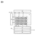
- FIG. 1 is a block diagram illustrating an imaging device.
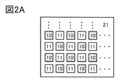
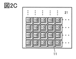
- 2A, 2B, and 2C are diagrams illustrating a pixel array.
- 3A, 3B, and 3C are diagrams illustrating a pixel circuit.
- 4A, 4B, and 4C are diagrams illustrating a pixel circuit.
- 5A, 5B, and 5C are diagrams illustrating a pixel circuit.
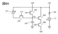
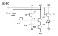
- 6A, 6B, and 6C are diagrams illustrating a pixel circuit.
- FIG. 7A is a diagram illustrating a rolling shutter system.
- FIG. 7B is a diagram illustrating the global shutter method.
- 8A and 8B are timing charts illustrating the operation of the pixel circuit.
- 9A and 9B are diagrams illustrating a pixel circuit.
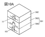
- 10A is a diagram illustrating a configuration of a pixel of an imaging device.
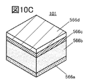
- 10B and 10C are diagrams illustrating the configuration of the photoelectric conversion device.
- FIG. 10D is a diagram illustrating a configuration of a light emitting device.
- 11A and 11B are diagrams illustrating a configuration of a pixel of the imaging device.
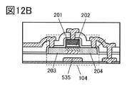
- 12A, 12B, 12C, and 12D are diagrams illustrating a transistor.
- 13A, 13B, and 13C are perspective views of a package containing the imaging device.
- 14A, 14B, and 14C are diagrams illustrating electronic devices.
- the element may be configured by a plurality of elements unless there is a functional inconvenience.
- a plurality of transistors operating as switches may be connected in series or in parallel.
- a capacitor also referred to as a capacitor
- one conductor may have a plurality of functions such as a wiring, an electrode, and a terminal in some cases, and in this specification, a plurality of names may be used for the same element.
- a plurality of names may be used for the same element.
- the elements may actually be connected via a plurality of conductors. In this document, such a configuration is also included in the category of direct connection.
- One embodiment of the present invention is an imaging device including a light-emitting device (also referred to as a light-emitting element). Light is emitted from a light emitting device to a subject, and light reflected from the subject is received by a photoelectric conversion device (also referred to as a photoelectric conversion element) included in the pixel circuit. Since an EL element is used for the light emitting device, a thin imaging device with a light source can be formed.
- an element that emits infrared light as a light emitting device, it can be used for applications such as biometric authentication and failure analysis of industrial products.
- a pixel circuit which is easily applied to imaging by the global shutter method an image without distortion can be obtained even for a moving subject.
- FIG. 1 is a block diagram illustrating an imaging device of one embodiment of the present invention.
- the imaging device has a pixel array 21 having pixel circuits 10 arranged in a matrix, a circuit 22 (row driver) having a function of selecting a row of the pixel array 21, and a function of reading data from the pixel circuit 10.
- the circuit includes a circuit 23 and a circuit 28 for supplying a power supply potential.
- the light emitting device 11 is stacked on the pixel circuit 10.
- the circuit 23 includes a circuit 24 (column driver) having a function of selecting a column of the pixel array 21, a circuit 25 (CDS circuit) for performing correlated double sampling processing on output data of the pixel circuit 10, and a circuit A circuit 26 (A / D conversion circuit or the like) having a function of converting analog data output from the analog data 25 into digital data can be provided.
- a circuit 24 column driver
- CDS circuit circuit 25
- a circuit 26 A / D conversion circuit or the like
- the pixel circuit 10 and the light emitting device 11 may be configured not to overlap.
- the pixel circuits 10 and the light emitting devices 11 may be alternately arranged at regular intervals.
- the pixel circuits 10 and the light emitting devices 11 may be alternately arranged for each row. Note that the pixel circuits 10 and the light emitting devices 11 may be alternately arranged for each column.
- a configuration in which a light emitting device 11 is arranged between two adjacent pixel circuits 10 may be employed.
- the light emitting device 11 is arranged so as to have a region overlapping with a wiring connected to the pixel circuit 10. Therefore, in a broad sense, it can be said that the pixel circuit 10 and the light emitting device 11 overlap.
- 2C shows the same number of light emitting devices 11 as the pixel circuits 10, but the number of light emitting devices 11 may be different from that of the pixel circuits 10.
- FIG. 3A is a circuit diagram illustrating a pixel circuit 10 and a light-emitting device 11 that can be used for the imaging device of one embodiment of the present invention.
- the pixel circuit 10 can include a photoelectric conversion device 101, a transistor 103, a transistor 104, a transistor 105, a transistor 106, and a capacitor 108. Note that a structure without the capacitor 108 may be employed.
- One electrode (cathode) of the photoelectric conversion device 101 is electrically connected to one of a source and a drain of the transistor 103.
- the other of the source and the drain of the transistor 103 is electrically connected to one of the source and the drain of the transistor 104.
- One of a source and a drain of the transistor 104 is electrically connected to one electrode of the capacitor 108.
- One electrode of the capacitor 108 is electrically connected to the gate of the transistor 105.
- One of a source and a drain of the transistor 105 is electrically connected to one of a source and a drain of the transistor 106.
- a wiring that connects the other of the source and the drain of the transistor 103, one electrode of the capacitor 108, and the gate of the transistor 105 is referred to as a node FD.
- the node FD can function as a charge storage unit.
- the other electrode (anode) of the photoelectric conversion device 101 is electrically connected to the wiring 121.
- the gate of the transistor 103 is electrically connected to the wiring 127.
- the other of the source and the drain of the transistor 104 and the other of the source and the drain of the transistor 105 are electrically connected to a wiring 122.
- the gate of the transistor 104 is electrically connected to the wiring 126.
- the gate of the transistor 106 is electrically connected to the wiring 128.
- the other electrode of the capacitor 108 is electrically connected to a reference potential line such as a GND wiring, for example.
- the other of the source and the drain of the transistor 106 is electrically connected to the wiring 129.
- one electrode of the light emitting device 11 is electrically connected to the wiring 130.
- the other electrode of the light emitting device 11 is electrically connected to a reference potential line such as a GND wiring, for example.
- a reference potential line such as a GND wiring
- the wirings 127 and 128 can function as signal lines for controlling conduction of each transistor.
- the wiring 129 can function as an output line.
- the wirings 121, 122, and 130 can function as power supply lines.
- the cathode side of the photoelectric conversion device 101 is electrically connected to the transistor 103, and the node FD is reset to a high potential to operate. Is also a high potential).
- the wiring 130 has a function of supplying a potential for supplying a forward bias to the light emitting device 11 to emit light.
- FIG. 3B illustrates a configuration in which one electrode of the light-emitting device 11 is electrically connected to the wiring 122.
- the reset potential of the node FD, the power supply potential supplied to the transistor 105, and the input potential of the light-emitting device 11 can be shared, such a structure can be employed.
- a transistor 107 may be added to the structure of FIG. 3B.
- One of a source and a drain of the transistor 107 is electrically connected to one electrode of the light-emitting device 11.
- the other of the source and the drain of the transistor 107 is electrically connected to the wiring 122.
- the gate of the transistor 107 is electrically connected to the wiring 127.
- the resistance element 109 is connected between one electrode of the light emitting device 11 and the wiring 122 as shown in FIG. May be electrically connected.
- the resistance element 109 acts as a current limiting resistor, can limit the current flowing through the light emitting device 11, and can increase the reliability of the light emitting device 11.
- An appropriate value may be selected for the resistance value of the resistance element 109 in accordance with the electrical characteristics of the light emitting device 11.
- the transistor 107 shown in FIG. 3C may be operated instead of the resistor 109.
- the gate of the transistor 107 is electrically connected to the wiring 131. Therefore, by changing the potential of the wiring 131, the illuminance and the light emission timing of the light emitting device 11 can be arbitrarily controlled, and power consumption can be suppressed.
- the transistor 107 is provided.
- the other of the source and the drain of the transistor 107 is electrically connected to the wiring 130, and the gate of the transistor 107 is electrically connected to the wiring 127.
- It may be a configuration. In this structure, the input potential to the light emitting device 11 is controlled by the wiring 130, and the timing of light emission is controlled by the wiring 127.
- FIGS. 4A to 4C show the structure in which the cathode of the photoelectric conversion device 101 is electrically connected to the node FD.
- the cathode of the photoelectric conversion device 101 may be electrically connected to the node FD.
- one electrode of the photoelectric conversion device 101 is electrically connected to the wiring 122, and the other electrode of the photoelectric conversion device 101 is connected to the source or the drain of the transistor 103. It is electrically connected to one. The other of the source and the drain of the transistor 104 is electrically connected to the wiring 132.
- the wiring 132 can function as a power supply line or a reset potential supply line. 5A to 5C and FIGS. 6A to 6C, the anode side of the photoelectric conversion device 101 is electrically connected to the transistor 103, and the node FD is reset to a low potential to operate.
- the wiring 132 has a low potential (a lower potential than the wiring 122).
- FIGS. 5A to 5C and FIGS. 6A to 6C can be referred to the description of FIGS. 3A to 3C and FIGS. 4A to 4C for the connection mode with the light emitting device 11 and its peripheral elements.
- a photodiode can be used as the photoelectric conversion device 101.
- imaging using infrared light is performed. Therefore, a photodiode capable of photoelectrically converting light in the infrared region is used for the photoelectric conversion device 101.
- a photodiode capable of photoelectrically converting light in the infrared region is used for the photoelectric conversion device 101.
- a pn junction photodiode using single crystal silicon for a photoelectric conversion portion a pin photodiode using polycrystalline silicon or microcrystalline silicon for a photoelectric conversion layer, or the like can be used.
- a material that can photoelectrically convert light in the infrared region such as a compound semiconductor, may be used.
- the transistor 103 has a function of controlling the potential of the node FD.
- the transistor 104 has a function of resetting the potential of the node FD.
- the transistor 105 functions as a source follower circuit and can output the potential of the node FD to the wiring 129 as image data.
- the transistor 106 has a function of selecting a pixel to output image data.
- a transistor including a metal oxide in a channel formation region (hereinafter, an OS transistor) is preferably used.
- the OS transistor has a characteristic of extremely low off-state current. With the use of the OS transistors as the transistors 103 and 104, the period during which charge can be held at the node FD can be extremely long. Therefore, it is possible to apply a global shutter method in which charge accumulation operation is simultaneously performed in all pixels without complicating a circuit configuration and an operation method.
- FIG. 7A is a diagram schematically illustrating the operation method of the rolling shutter system
- FIG. 7B is a diagram schematically illustrating the global shutter system.
- En represents the exposure (accumulation operation) of the n-th column (n is a natural number)
- Rn represents the read operation of the n-th column.
- 7A and 7B show the operation from the first row to the M-th row (M is a natural number).
- the rolling shutter method is an operation method of sequentially performing exposure and data reading, and is a method in which a reading period of a certain row and an exposure period of another row are overlapped. Since the reading operation is performed immediately after the exposure, imaging can be performed even with a circuit configuration in which the data retention period is relatively short. However, since an image of one frame is composed of data having no synchronization at the time of imaging, distortion occurs in imaging of a moving object.
- the global shutter method is an operation method in which exposure is performed simultaneously on all pixels, data is held in each pixel, and data is read out for each row. Therefore, an image without distortion can be obtained even when capturing a moving object.
- a transistor having a relatively high off-state current such as a transistor using Si (hereinafter referred to as a Si transistor) in a channel formation region
- Si transistor a transistor using Si
- a rolling shutter method is used because a data potential easily flows out of a charge storage portion.
- the global shutter method using Si transistors it is necessary to separately provide a memory circuit and the like, and further complicated operations must be performed at high speed.
- the OS transistor is used for the pixel circuit, the global shutter method can be easily realized because there is almost no outflow of the data potential from the charge storage portion.
- an OS transistor may be used as the transistors 105 and 106. Further, an OS transistor and a Si transistor may be arbitrarily combined and applied. Further, all the transistors may be OS transistors or Si transistors. Examples of the Si transistor include a transistor including amorphous silicon, a transistor including crystalline silicon (typically, low-temperature polysilicon, single crystal silicon, and the like).
- an EL element can be used.
- the EL element an element that emits infrared light can be used.
- an EL element which emits near-infrared light having a peak at a wavelength of 700 nm or more and 2500 nm or less is preferable.
- the position of a vein can be detected by receiving reflected light from a palm or a finger and forming an image. This effect can be used as biometric authentication.
- it can be used for nondestructive inspection such as inspection of foreign substances in food or failure analysis of industrial products using near infrared light having an appropriate wavelength.
- highly accurate sensing can be performed even if the subject moves.
- a thin imaging device with a light source can be realized, which can be easily mounted on various devices, and portability can be improved.
- the light emitting device 11 is in a state in which a power supply potential for appropriately emitting light is supplied to the light emitting device 11 at least during the accumulation operation.
- the transistor 104 is turned off and supply of a reset potential is cut off. Further, the potential of the node FD decreases in accordance with the operation of the photoelectric conversion device 101 (accumulation operation).
- the pixel circuits 10 shown in FIGS. 5A to 5C and 6A to 6C can be operated according to the timing chart of FIG. 8B. It is assumed that “H” is always supplied to the wiring 122 and “L” is always supplied to the wiring 132. The basic operation is the same as that described in the timing chart of FIG. 8A.
- a transistor may be provided with a back gate as illustrated in FIGS. 9A and 9B.
- FIG. 9A shows a configuration in which the back gate is electrically connected to the front gate, which has an effect of increasing the on-state current.
- FIG. 9B illustrates a structure in which the back gate is electrically connected to a wiring which can supply a constant potential, so that the threshold voltage of the transistor can be controlled.
- the pixel circuit may include a transistor without a back gate. Note that the structure in which the transistor is provided with a back gate can be applied to all the structures illustrated in FIGS. 3A to 3C, FIGS. 4A to 4C, FIGS. 5A to 5C, and FIGS. 6A to 6C.
- FIG. 10A illustrates a structure of a pixel included in the imaging device.
- the pixel can have a stacked structure of a layer 561 including the pixel circuit 10 and a layer 562 including the light-emitting device 11.
- the layer 561 includes a layer 563 and a layer 564. Elements such as transistors included in the pixel circuit 10 are mainly provided in the layer 563.
- the layer 564 is mainly provided with the photoelectric conversion device 101.
- the photoelectric conversion device 101 can be a stack of a layer 565a and a layer 565b as illustrated in FIG. 10B.
- the photoelectric conversion device 101 illustrated in FIG. 10B is a pn junction photodiode.
- a p-type semiconductor can be used for the layer 565a and an n-type semiconductor can be used for the layer 565b.
- an n-type semiconductor may be used for the layer 565a and a p-type semiconductor may be used for the layer 565b.
- the layer 566a may be an n-type semiconductor and the layer 566c may be a p-type semiconductor.
- the pn junction photodiode can be formed using single crystal silicon. Further, the pin junction photodiode can be formed using a thin film of single crystal silicon, microcrystalline silicon, polycrystalline silicon, or the like. Monocrystalline silicon, microcrystalline silicon, and polycrystalline silicon have sensitivity to infrared light and are suitable for detecting infrared light.
- a silicon substrate can be used as the layer 564 illustrated in FIG. 10A.
- the silicon substrate can include a Si transistor or the like in addition to the pn junction photodiode.
- a circuit for driving a pixel circuit, a circuit for reading an image signal, an image processing circuit, or the like can be provided using the Si transistor.
- part or all of the transistors described in Embodiment 1 and included in the peripheral circuits can be provided in the layer 564.
- the layer 564 may have a structure including a support having an insulating surface such as a glass substrate and the above-described pin junction photodiode.
- the layer 563 can include an OS transistor (for example, part or all of the transistors 103, 104, 105, 106, and 107 included in the pixel circuit 10). Further, some of the transistors included in the peripheral circuit described in Embodiment 1 may be included.
- the element and the peripheral circuit included in the pixel circuit can be dispersed in a plurality of layers and the element or the element and the peripheral circuit can be provided in an overlapping manner; thus, the area of the imaging device can be reduced. be able to.
- a metal oxide having an energy gap of 2 eV or more, preferably 2.5 eV or more, more preferably 3 eV or more can be used.
- an oxide semiconductor containing indium or the like is used.
- CAAC-OS CAC-Aligned Crystalline Oxide Semiconductor
- CAC-OS Cloud-Aligned Composite Oxide Semiconductor
- the CAAC-OS has stable atoms in its crystal and is suitable for a transistor or the like in which reliability is emphasized.
- the CAC-OS has high mobility characteristics, and thus is suitable for a transistor that drives at high speed or the like.
- the OS transistor has an extremely low off-current characteristic of several yA / ⁇ m (current value per 1 ⁇ m of channel width) because the energy gap of the semiconductor layer is large. Further, the OS transistor has characteristics different from those of the Si transistor, such as not generating impact ionization, avalanche breakdown, and a short-channel effect, and thus can form a highly reliable circuit with high withstand voltage. In addition, variation in electrical characteristics due to non-uniformity of crystallinity, which is a problem in the Si transistor, hardly occurs in the OS transistor.
- the semiconductor layer included in the OS transistor includes an In-M-Zn-based oxide including, for example, indium, zinc, and M (a metal such as aluminum, titanium, gallium, germanium, yttrium, zirconium, lanthanum, cerium, tin, neodymium, or hafnium). Can be obtained.
- the In-M-Zn-based oxide can be typically formed by a sputtering method. Alternatively, it may be formed by using an ALD (Atomic layer deposition) method.
- the atomic ratio of metal elements of a sputtering target used for forming the In-M-Zn-based oxide by a sputtering method satisfy In ⁇ M and Zn ⁇ M.
- each of the atomic ratios of the semiconductor layers to be formed includes a variation of ⁇ 40% of the atomic ratio of the metal element contained in the sputtering target.
- the semiconductor layer an oxide semiconductor with a low carrier density is used.
- the semiconductor layer has a carrier density of 1 ⁇ 10 17 / cm 3 or less, preferably 1 ⁇ 10 15 / cm 3 or less, further preferably 1 ⁇ 10 13 / cm 3 or less, more preferably 1 ⁇ 10 11 / cm 3. 3 or less, more preferably less than 1 ⁇ 10 10 / cm 3 , and an oxide semiconductor of 1 ⁇ 10 ⁇ 9 / cm 3 or more can be used.
- Such an oxide semiconductor is referred to as a high-purity intrinsic or substantially high-purity intrinsic oxide semiconductor. It can be said that the oxide semiconductor has a low density of defect states and has stable characteristics.
- this embodiment is not limited thereto, and an oxide semiconductor having an appropriate composition may be used depending on required semiconductor characteristics and electric characteristics (eg, field-effect mobility and threshold voltage) of the transistor.
- the carrier density and the impurity concentration of the semiconductor layer, the defect density, the atomic ratio between a metal element and oxygen, the interatomic distance, and the density be appropriate.
- the concentration of silicon or carbon (concentration obtained by secondary ion mass spectrometry (SIMS)) in the semiconductor layer is set to 2 ⁇ 10 18 atoms / cm 3 or less, preferably 2 ⁇ 10 17 atoms / cm 3 or less. / Cm 3 or less.
- an alkali metal and an alkaline earth metal may generate carriers when combined with an oxide semiconductor, which may increase off-state current of a transistor.
- concentration of the alkali metal or alkaline earth metal (concentration obtained by SIMS) in the semiconductor layer is set to 1 ⁇ 10 18 atoms / cm 3 or less, preferably 2 ⁇ 10 16 atoms / cm 3 or less.
- the nitrogen concentration (concentration obtained by SIMS) in the semiconductor layer is preferably 5 ⁇ 10 18 atoms / cm 3 or less.
- the transistor when hydrogen is contained in the oxide semiconductor included in the semiconductor layer, oxygen reacts with oxygen bonded to a metal atom to become water, which may cause oxygen vacancies in the oxide semiconductor.
- oxygen vacancy When an oxygen vacancy is contained in a channel formation region in an oxide semiconductor, the transistor might have normally-on characteristics. Further, a defect in which hydrogen is contained in an oxygen vacancy functions as a donor, and an electron serving as a carrier may be generated. Further, in some cases, part of hydrogen is bonded to oxygen which is bonded to a metal atom to generate electrons serving as carriers. Therefore, a transistor including an oxide semiconductor containing a large amount of hydrogen is likely to have normally-on characteristics.
- a defect in which hydrogen is contained in oxygen vacancies can function as a donor of an oxide semiconductor.
- the hydrogen concentration obtained by SIMS is lower than 1 ⁇ 10 20 atoms / cm 3 , preferably lower than 1 ⁇ 10 19 atoms / cm 3 , and more preferably lower than 5 ⁇ 10 18 atoms / cm 3. It is set to less than 3 , more preferably less than 1 ⁇ 10 18 atoms / cm 3 .
- an oxide semiconductor in which impurities such as hydrogen are sufficiently reduced is used for a channel formation region of a transistor, stable electric characteristics can be provided.
- the semiconductor layer may have a non-single-crystal structure, for example.
- the non-single-crystal structure includes, for example, a CAAC-OS having c-axis aligned crystals, a polycrystalline structure, a microcrystalline structure, or an amorphous structure.
- the amorphous structure has the highest density of defect states
- the CAAC-OS has the lowest density of defect states.
- An oxide semiconductor film having an amorphous structure has, for example, a disordered atomic arrangement and no crystalline component.
- an oxide film having an amorphous structure has, for example, a completely amorphous structure and no crystal part.
- the semiconductor layer is a mixed film including two or more of an amorphous structure region, a microcrystalline structure region, a polycrystalline structure region, a CAAC-OS region, and a single crystal structure region.
- the mixed film may have a single-layer structure or a stacked structure including any two or more of the above-described regions.
- CAC-OS which is one embodiment of a non-single-crystal semiconductor layer is described below.
- the CAC-OS is one structure of a material in which an element included in an oxide semiconductor is unevenly distributed in a size of, for example, 0.5 nm or more and 10 nm or less, preferably 1 nm or more and 2 nm or less.
- one or more metal elements are unevenly distributed in an oxide semiconductor, and a region including the metal element has a size of 0.5 nm to 10 nm, preferably 1 nm to 2 nm, or a size in the vicinity thereof.
- the state mixed by is also referred to as a mosaic shape or a patch shape.
- the oxide semiconductor preferably contains at least indium. In particular, it preferably contains indium and zinc. In addition to them, aluminum, gallium, yttrium, copper, vanadium, beryllium, boron, silicon, titanium, iron, nickel, germanium, zirconium, molybdenum, lanthanum, cerium, neodymium, hafnium, tantalum, tungsten, or magnesium, etc. Or a plurality of types selected from the group consisting of:
- CAC-OS in an In-Ga-Zn oxide is an indium oxide (hereinafter referred to as InO).
- InO indium oxide
- X1 X1 is greater real than 0
- X2 Zn Y2 O Z2 X2, Y2, and Z2 is larger real than 0
- gallium An oxide hereinafter, referred to as GaO X3 (X3 is a real number larger than 0)
- Ga X4 Zn Y4 O Z4 X4, Y4, and Z4 are real numbers larger than 0)
- the material becomes mosaic by separate into, mosaic InO X1 or in X2 Zn Y2 O Z2, is a configuration in which uniformly distributed in the film (hereinafter Also referred to as a cloud-like
- the CAC-OS is a composite oxide semiconductor having a structure in which a region containing GaO X3 as a main component and a region containing In X2 Zn Y2 O Z2 or InO X1 as a main component are mixed.
- the atomic ratio of In to the element M in the first region is larger than the atomic ratio of In to the element M in the second region.
- the In concentration is higher than that of the region No. 2.
- IGZO is a common name and may refer to one compound of In, Ga, Zn, and O. Representative examples are represented by InGaO 3 (ZnO) m1 (m1 is a natural number), or In (1 + x0) Ga ( 1-x0) O 3 (ZnO) m0 (-1 ⁇ x0 ⁇ 1, m0 is an arbitrary number) Crystalline compounds may be mentioned.
- the above crystalline compound has a single crystal structure, a polycrystal structure, or a CAAC structure.
- the CAAC structure is a crystal structure in which a plurality of IGZO nanocrystals have a c-axis orientation and are connected without being oriented in the ab plane.
- CAC-OS relates to the material configuration of an oxide semiconductor.
- a CAC-OS is a material composition containing In, Ga, Zn, and O, a region which is observed as a nanoparticle mainly containing Ga as a part, and a nanoparticle mainly containing In as a part.
- a region observed in a shape means a configuration in which each region is randomly dispersed in a mosaic shape. Therefore, in the CAC-OS, the crystal structure is a secondary element.
- the CAC-OS does not include a stacked structure of two or more kinds of films having different compositions.
- a structure including two layers of a film mainly containing In and a film mainly containing Ga is not included.
- the CAC-OS has a region which is observed in the form of a nanoparticle mainly including the metal element and a nanoparticle mainly including In as a part.
- the region observed in the form of particles refers to a configuration in which each of the regions is randomly dispersed in a mosaic shape.
- the CAC-OS can be formed by a sputtering method, for example, without intentionally heating the substrate.
- any one or more selected from an inert gas (typically, argon), an oxygen gas, and a nitrogen gas is used as a deposition gas.
- the flow rate ratio of the oxygen gas to the total flow rate of the film formation gas during the film formation is preferably as low as possible.
- the flow rate ratio of the oxygen gas is preferably from 0% to less than 30%, more preferably from 0% to 10%. .
- the CAC-OS is characterized in that a clear peak is not observed when measured using a ⁇ / 2 ⁇ scan by an Out-of-plane method, which is one of X-ray diffraction (XRD) measurement methods.
- XRD X-ray diffraction
- the CAC-OS includes, in an electron beam diffraction pattern obtained by irradiating an electron beam (also referred to as a nanobeam electron beam) with a probe diameter of 1 nm, a ring-shaped region (ring region) with high luminance and a ring-shaped region. Multiple bright spots are observed in the area. Therefore, the electron diffraction pattern shows that the crystal structure of the CAC-OS has an nc (nano-crystal) structure having no orientation in a planar direction and a cross-sectional direction.
- an electron beam also referred to as a nanobeam electron beam
- GaO X3 is a main component by EDX mapping acquired using energy dispersive X-ray spectroscopy (EDX). It can be confirmed that the region and the region containing In X2 Zn Y2 O Z2 or InO X1 as a main component are unevenly distributed and mixed.
- EDX energy dispersive X-ray spectroscopy
- the CAC-OS has a different structure from an IGZO compound in which metal elements are uniformly distributed, and has different properties from the IGZO compound.
- the CAC-OS is phase-separated into a region containing GaO X3 or the like as a main component and a region containing In X2 Zn Y2 O Z2 or InO X1 as a main component.
- the region in which In X2 Zn Y2 O Z2 or InO X1 is a main component is a region having higher conductivity than the region in which GaO X3 or the like is a main component. That is, the conductivity of the oxide semiconductor is exhibited by the flow of carriers in a region containing In X2 Zn Y2 O Z2 or InO X1 as a main component. Therefore, high field-effect mobility ( ⁇ ) can be realized by distributing a region containing In X2 Zn Y2 O Z2 or InO X1 as a main component in a cloud shape in the oxide semiconductor.
- a region containing GaO X3 or the like as a main component is a region having higher insulating properties as compared with a region containing In X2 Zn Y2 O Z2 or InO X1 as a main component. That is, a region in which GaO X3 or the like is a main component is distributed in the oxide semiconductor, whereby a leakage current can be suppressed and a favorable switching operation can be realized.
- the insulating property caused by GaO X3 or the like and the conductivity caused by In X2 Zn Y2 O Z2 or InO X1 act complementarily to each other, so that high performance is obtained.
- On-state current (I on ) and high field-effect mobility ( ⁇ ) can be realized.
- CAC-OS is suitable as a constituent material of various semiconductor devices.
- the layer 562 has the light emitting device 11.
- a light emitting device (EL element) using electroluminescence can be applied.
- An EL element has a layer containing a light-emitting compound (EL layer) between a pair of electrodes. When a potential difference larger than the threshold voltage of the EL element is generated between the pair of electrodes, holes are injected from the anode side into the EL layer and electrons are injected from the cathode side. The injected electrons and holes are recombined in the EL layer, and the light-emitting substance contained in the EL layer emits light.
- an organic EL element or an inorganic EL element can be used.
- an LED including a mini LED and a micro LED
- a compound semiconductor as a light emitting material
- an organic EL element by applying a voltage, electrons are injected from one electrode and holes are injected from the other electrode into the EL layer. Then, by recombination of the carriers (electrons and holes), the light-emitting organic compound forms an excited state and emits light when the excited state returns to the ground state. Due to such a mechanism, such a light-emitting device is called a current-excitation light-emitting device.
- the EL layer can be formed by a method such as an evaporation method (including a vacuum evaporation method), a transfer method, a printing method, an inkjet method, and a coating method.
- a method such as an evaporation method (including a vacuum evaporation method), a transfer method, a printing method, an inkjet method, and a coating method.
- the inorganic EL elements are classified according to their element structures into a dispersion-type inorganic EL element and a thin-film inorganic EL element.
- the dispersion-type inorganic EL element has a light-emitting layer in which particles of a light-emitting material are dispersed in a binder.
- the light-emission mechanism is donor-acceptor recombination light emission using a donor level and an acceptor level.
- the thin-film inorganic EL device has a structure in which a light-emitting layer is sandwiched between dielectric layers and further sandwiched between electrodes. The light-emitting mechanism is localized light emission using inner-shell electron transition of metal ions.
- FIG. 10D shows a configuration of the light emitting device 11.
- the EL layer 300 can include a plurality of layers such as a layer 330, a light-emitting layer 320, and a layer 340.
- the layer 330 can include, for example, a layer containing a substance having a high electron-injection property (an electron-injection layer), a layer containing a substance having a high electron-transport property (an electron-transport layer), or the like.
- the light-emitting layer 320 includes, for example, a light-emitting compound.
- the layer 340 can include, for example, a layer containing a substance having a high hole-injection property (a hole-injection layer) and a layer containing a substance having a high hole-transport property (a hole-transport layer).
- the EL layer 300 provided between the electrode 311 and the electrode 312 can function as a single light-emitting unit. Note that a plurality of light-emitting layers may be provided between the layer 330 and the layer 340. Note that the light emission direction is determined by using a light-transmitting conductive film for one of the electrode 311 and the electrode 312.
- the light emitting device 11 can emit light of various wavelengths depending on the material forming the EL layer 300.
- a material which emits light having a peak in near-infrared light (wavelength: 720 nm to 2500 nm) is used for a material of the EL layer 300.
- a material which emits light having a wavelength of 720 nm, 760 nm, 850 nm, 900 nm, or a wavelength near these wavelengths may be used depending on the application.
- the light-emitting material (also referred to as a guest material or a dopant material) of the EL layer 300 preferably includes an organometallic iridium complex that emits near-infrared light.
- the organometallic iridium complex preferably has a dimethylphenyl skeleton and a quinoxaline skeleton.
- organometallic iridium complex typically, bis ⁇ 4,6-dimethyl-2- [3- (3,5-dimethylphenyl) -2-quinoxalinyl- ⁇ N] phenyl- ⁇ C ⁇ (2, 2 ′, 6,6′-Tetramethyl-3,5-heptanedionato- ⁇ 2 O, O ′) iridium (III) (abbreviation: Ir (dmdpq) 2 (dpm)) or the like can be used.
- Ir (dmdpq) 2 (dpm) iridium
- an imaging element with high quantum efficiency or high luminous efficiency can be provided.
- a substance that is, a host material used to make the organometallic iridium complex in a dispersed state
- TPAQn 2,3-bis (4-diphenylaminophenyl) quinoxaline
- TPAQn 2,3-bis (4-diphenylaminophenyl) quinoxaline
- TPAQn 2,3-bis (4-diphenylaminophenyl) quinoxaline
- TPAQn 2,3-bis (4-diphenylaminophenyl) quinoxaline
- TPAQn 2,3-bis (4-diphenylaminophenyl) quinoxaline
- TPAQn 2,3-bis (4-diphenylaminophenyl) quinoxaline
- TPAQn 2,3-bis (4-diphenylaminophenyl) quinoxaline
- TPAQn 2,3-bis (4-diphenylaminophenyl) quinoxaline
- TPAQn 2,3-bis (4-diphenyla
- N- (1,1′-biphenyl-4-yl) -N- [4- (9-phenyl-9H- Carbazol-3-yl) phenyl] -9,9-dimethyl-9H-fluoren-2-amine (abbreviation: PCBBiF) is preferably used.
- the light-emitting layer 320 including the above-described organometallic iridium complex (guest material) and the above-described host material, near-infrared phosphorescence with high emission efficiency can be obtained from the EL layer 300. Can be.
- FIG. 11A is a diagram illustrating an example of a cross section of the pixel illustrated in FIG. 10A.
- the layer 564 has the pn junction photodiode illustrated in FIG. 10B as the photoelectric conversion device 101.
- the layer 563 includes an OS transistor, and FIG. 11A illustrates the transistors 103 and 107 with the structure illustrated in FIG. 3C as an example.
- the layer 565a can be a p-type region and the layer 565b can be an n-type region. Further, the wiring 121 having a function of a power supply line is connected to the layer 565b.
- FIG. 12A shows details of the OS transistor.
- the OS transistor illustrated in FIG. 12A has a self-aligned structure in which an insulating layer is provided over a stack of an oxide semiconductor layer and a conductive layer, and an opening which reaches the semiconductor layer is provided, so that the source electrode 205 and the drain electrode 206 are formed. It is.
- the OS transistor can include a channel formation region, a source region 203, and a drain region 204 formed in the oxide semiconductor layer 207, a gate electrode 201, and a gate insulating film 202. At least the gate insulating film 202 and the gate electrode 201 are provided in the opening.
- the oxide semiconductor layer 208 may be further provided in the opening.
- the OS transistor may have a self-aligned structure in which a source region 203 and a drain region 204 are formed in a semiconductor layer using the gate electrode 201 as a mask.
- a non-self-aligned top-gate transistor having a region where the source electrode 205 or the drain electrode 206 and the gate electrode 201 overlap with each other may be used.
- the transistors 103 and 107 have a structure including the back gate 535, a structure without a back gate may be employed.
- the back gate 535 may be electrically connected to a front gate of a transistor provided opposite to the transistor as illustrated in a cross-sectional view in the channel width direction of the transistor illustrated in FIG. 12D.
- FIG. 12D shows the transistor of FIG. 12A as an example, the same applies to transistors having other structures.
- a configuration in which a fixed potential different from that of the front gate may be supplied to the back gate 535 may be employed.
- An insulating layer 543 having a function of preventing diffusion of hydrogen is provided between a region where an OS transistor is formed and a region where a Si device such as the photoelectric conversion device 101 is formed. Hydrogen in the insulating layer provided near the photoelectric conversion device 101 terminates dangling bonds of silicon. On the other hand, hydrogen in the insulating layer provided in the vicinity of the channel formation regions of the transistors 103 and 107 is one of the factors which generate carriers in the oxide semiconductor layer.
- the reliability of the Si device can be improved by confining hydrogen in one layer. Further, by suppressing diffusion of hydrogen from one layer to the other layer, reliability of the OS transistor (the transistors 103 and 107) can be improved.
- the insulating layer 543 for example, aluminum oxide, aluminum oxynitride, gallium oxide, gallium oxynitride, yttrium oxide, yttrium oxynitride, hafnium oxide, hafnium oxynitride, yttria-stabilized zirconia (YSZ), or the like can be used.
- aluminum oxide, aluminum oxynitride, gallium oxide, gallium oxynitride, yttrium oxide, yttrium oxynitride, hafnium oxide, hafnium oxynitride, yttria-stabilized zirconia (YSZ), or the like can be used.
- planarization films 541 and 542 are provided over the transistors 103 and 107.
- the light emitting device 11 (the electrode 311, the EL layer 300, and the electrode 312) is provided on a surface in which uneven portions generated in a transistor and a contact portion are flattened by the flattening films 541 and 542.
- a low-resistance conductive film such as a metal can be used.
- the electrode 312 a light-transmitting conductive film which transmits near-infrared light can be used.
- the electrode 312 includes indium oxide containing tungsten oxide, indium zinc oxide containing tungsten oxide, indium oxide containing titanium oxide, indium tin oxide, indium tin oxide containing titanium oxide, and indium zinc oxide.
- a light-transmitting conductive material such as indium tin oxide to which silicon oxide is added can be used.
- the EL layer 300 overlapping with the electrodes 311 and 312 can emit light, but the EL layer 300 overlapping with the electrode 312 and not overlapping with the electrode 311 cannot emit light. Further, the EL layer 300 is an extremely thin thin film, and the absorption of near-infrared light can be ignored. Therefore, the EL layer 300 and the electrode 312 can be provided over the photoelectric conversion device 101.
- FIG. 11A illustrates a region where the photoelectric conversion device 101 and the transistor 103 overlap each other, this region is a part of the entire light receiving portion and does not significantly reduce light receiving ability. Note that a structure in which the photoelectric conversion device 101 and the transistor 103 do not have an overlapping region may be employed.
- light 601 is emitted from the light-emitting device 11 included in the layer 562 to the outside, and the reflected light 602 is received by the photoelectric conversion device 101 included in the layer 564 through the layers 562 and 563.
- a sealing layer 590 be provided between the light emitting device 11 and the substrate 580 to seal the light emitting device 11 so that oxygen, hydrogen, moisture, carbon dioxide, and the like do not enter the light emitting device 11.
- an ultraviolet curable resin or a thermosetting resin can be used, such as PVC (polyvinyl chloride), an acrylic resin, a polyimide, an epoxy resin, or a silicone resin. Resin, PVB (polyvinyl butyral) or EVA (ethylene vinyl acetate) can be used.
- a desiccant may be included in the sealing layer 590.
- a protective layer such as silicon nitride, silicon nitride oxide, aluminum oxide, aluminum nitride, aluminum oxynitride, aluminum nitride oxide, or DLC (Diamond Like Carbon) may be provided.
- FIG. 11B is a diagram illustrating an example of a cross section of a pixel when the pin junction photodiode illustrated in FIG. 10C is used as the photoelectric conversion device 101.
- the layer 566a can be a p-type region
- the layer 566b can be an i-type region
- the layer 566c can be an n-type region.
- the wiring 121 having a function of a power supply line is connected to the layer 566a.
- the photoelectric conversion device 101 and the wiring 121 are provided over a substrate 570.
- a substrate such as a glass substrate, a ceramics substrate, or a resin substrate having an insulating surface can be used.
- a metal substrate or a semiconductor substrate may be used as long as the surface has been subjected to an insulating treatment.
- the configuration of the imaging device with a light source can be used.
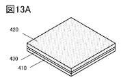
- FIG. 13A is an external perspective view of an upper surface side of a package containing an image sensor chip.
- the package includes a package substrate 410 for fixing the image sensor chip 450, a cover glass 420, an adhesive 430 for bonding the two, and the like.
- FIG. 13B is an external perspective view of the lower surface side of the package.
- a BGA Bit grid array
- BGA All grid array
- LGA Land Grid Array
- PGA Peripheral Component Interconnect
- FIG. 13C is a perspective view of the package illustrated with the cover glass 420 and a part of the adhesive 430 omitted.
- An electrode pad 460 is formed on the package substrate 410, and the electrode pad 460 and the bump 440 are electrically connected through a through hole.
- the electrode pad 460 is electrically connected to the image sensor chip 450 by a wire 470.
- the image sensor chip By mounting the image sensor chip in the above-described package, mounting on a printed circuit board or the like becomes easy, and the image sensor chip can be incorporated in various electronic devices.
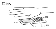
- FIG. 14A illustrates a biometric authentication device, which includes a thin housing 911, operation buttons 912, a detection unit 913, and the like.
- the shape of a vein can be recognized by holding a hand or a finger over the detection unit 913 or by closely touching the detection unit 913.
- the acquired data can be transmitted to the server by the wireless communication unit 914 and collated with the database to identify an individual.
- a personal identification number or the like can be input using the operation buttons.
- the imaging device 915 according to one embodiment of the present invention is provided immediately below the detection portion, and does not require another light source; thus, a thin authentication device can be formed. By being thin, it can be easily incorporated into various devices. Also, portability is improved.
- FIG. 14B illustrates a nondestructive inspection device including a housing 921, an operation panel 922, a transport mechanism 923, a monitor 924, a detection unit 925, and the like.
- the inspected member 926 is transported by the transport mechanism 923 directly below the detection unit 925.
- the inspected member 926 is imaged by the imaging device 927 of one embodiment of the present invention provided in the detection unit 925, and the captured image is displayed on the monitor 924. After that, it is transported to the outlet of the housing 921, and the defective product is separated and collected.
- the imaging device 915 of one embodiment of the present invention does not require another light source, the detection unit 925 can be formed at low cost.
- FIG. 14C illustrates a food sorting device, which includes a housing 931, operation buttons 932, a display portion 933, a light-shielding hood 934, and the like.
- a food sorting device which includes a housing 931, operation buttons 932, a display portion 933, a light-shielding hood 934, and the like.
- the imaging device 935 of one embodiment of the present invention provided in the light receiving portion does not require another light source, a thin, lightweight, and portable food sorting device can be formed at low cost.
- the configuration shown in FIG. 14B may be used as a food sorting device.
- the configuration shown in FIG. 14C may be used as a non-destructive inspection device.
Landscapes
- Engineering & Computer Science (AREA)
- Multimedia (AREA)
- Signal Processing (AREA)
- Thin Film Transistor (AREA)
- Solid State Image Pick-Up Elements (AREA)
- Transforming Light Signals Into Electric Signals (AREA)
Priority Applications (3)
| Application Number | Priority Date | Filing Date | Title |
|---|---|---|---|
| JP2020540870A JP7350753B2 (ja) | 2018-09-07 | 2019-08-26 | 撮像装置および電子機器 |
| US17/273,032 US20210351224A1 (en) | 2018-09-07 | 2019-08-26 | Imaging Device and Electronic Device |
| CN201980056722.XA CN112640107A (zh) | 2018-09-07 | 2019-08-26 | 摄像装置及电子设备 |
Applications Claiming Priority (2)
| Application Number | Priority Date | Filing Date | Title |
|---|---|---|---|
| JP2018-167669 | 2018-09-07 | ||
| JP2018167669 | 2018-09-07 |
Publications (1)
| Publication Number | Publication Date |
|---|---|
| WO2020049398A1 true WO2020049398A1 (ja) | 2020-03-12 |
Family
ID=69723006
Family Applications (1)
| Application Number | Title | Priority Date | Filing Date |
|---|---|---|---|
| PCT/IB2019/057137 Ceased WO2020049398A1 (ja) | 2018-09-07 | 2019-08-26 | 撮像装置および電子機器 |
Country Status (4)
| Country | Link |
|---|---|
| US (1) | US20210351224A1 (https=) |
| JP (1) | JP7350753B2 (https=) |
| CN (1) | CN112640107A (https=) |
| WO (1) | WO2020049398A1 (https=) |
Cited By (2)
| Publication number | Priority date | Publication date | Assignee | Title |
|---|---|---|---|---|
| EP4222784A4 (en) * | 2020-10-08 | 2024-06-26 | Avicenatech Corp. | INTEGRATION OF OE COMPONENTS WITH ICS |
| JP2025508990A (ja) * | 2022-01-19 | 2025-04-10 | エックスオー セミコンダクタ インコーポレイテッド | Spadアレイを用いるイメージセンサー |
Families Citing this family (4)
| Publication number | Priority date | Publication date | Assignee | Title |
|---|---|---|---|---|
| KR101422362B1 (ko) | 2009-07-10 | 2014-07-22 | 가부시키가이샤 한도오따이 에네루기 켄큐쇼 | 표시 장치, 표시 패널 및 전자 기기 |
| WO2021009638A1 (ja) | 2019-07-17 | 2021-01-21 | 株式会社半導体エネルギー研究所 | 表示装置 |
| WO2021024070A1 (ja) | 2019-08-02 | 2021-02-11 | 株式会社半導体エネルギー研究所 | 機能パネル、表示装置、入出力装置、情報処理装置 |
| JPWO2021111227A1 (https=) | 2019-12-02 | 2021-06-10 |
Citations (6)
| Publication number | Priority date | Publication date | Assignee | Title |
|---|---|---|---|---|
| JP2002268615A (ja) * | 2000-12-14 | 2002-09-20 | Semiconductor Energy Lab Co Ltd | 半導体装置 |
| JP2004349907A (ja) * | 2003-05-21 | 2004-12-09 | Minolta Co Ltd | 固体撮像装置 |
| JP2010153449A (ja) * | 2008-12-24 | 2010-07-08 | Seiko Epson Corp | 光源一体型光電変換装置 |
| JP2012256020A (ja) * | 2010-12-15 | 2012-12-27 | Semiconductor Energy Lab Co Ltd | 半導体装置及びその駆動方法 |
| JP2015005280A (ja) * | 2013-05-20 | 2015-01-08 | 株式会社半導体エネルギー研究所 | 撮像パネル、撮像装置 |
| JP2015039165A (ja) * | 2013-07-19 | 2015-02-26 | 株式会社半導体エネルギー研究所 | 固体撮像装置、半導体表示装置 |
Family Cites Families (8)
| Publication number | Priority date | Publication date | Assignee | Title |
|---|---|---|---|---|
| JP4911446B2 (ja) | 2005-09-15 | 2012-04-04 | 富士フイルム株式会社 | エリアセンサ、画像入力装置、およびそれを組み込んだ電子写真装置等 |
| CN104393007A (zh) * | 2009-11-06 | 2015-03-04 | 株式会社半导体能源研究所 | 半导体装置 |
| JP5558446B2 (ja) | 2011-09-26 | 2014-07-23 | 株式会社東芝 | 光電変換装置及びその製造方法 |
| KR102205856B1 (ko) * | 2014-06-11 | 2021-01-21 | 삼성디스플레이 주식회사 | 센서를 포함하는 유기 발광 표시 장치 |
| TWI713367B (zh) * | 2015-07-07 | 2020-12-11 | 日商半導體能源研究所股份有限公司 | 成像裝置及其運作方法 |
| KR102456530B1 (ko) * | 2015-09-09 | 2022-10-20 | 삼성전자주식회사 | 이미지 센서 |
| US10896923B2 (en) * | 2015-09-18 | 2021-01-19 | Semiconductor Energy Laboratory Co., Ltd. | Method of operating an imaging device with global shutter system |
| CN109509767B (zh) * | 2017-09-15 | 2024-07-12 | 京东方科技集团股份有限公司 | 一种显示面板及显示装置 |
-
2019
- 2019-08-26 JP JP2020540870A patent/JP7350753B2/ja active Active
- 2019-08-26 WO PCT/IB2019/057137 patent/WO2020049398A1/ja not_active Ceased
- 2019-08-26 CN CN201980056722.XA patent/CN112640107A/zh active Pending
- 2019-08-26 US US17/273,032 patent/US20210351224A1/en active Pending
Patent Citations (6)
| Publication number | Priority date | Publication date | Assignee | Title |
|---|---|---|---|---|
| JP2002268615A (ja) * | 2000-12-14 | 2002-09-20 | Semiconductor Energy Lab Co Ltd | 半導体装置 |
| JP2004349907A (ja) * | 2003-05-21 | 2004-12-09 | Minolta Co Ltd | 固体撮像装置 |
| JP2010153449A (ja) * | 2008-12-24 | 2010-07-08 | Seiko Epson Corp | 光源一体型光電変換装置 |
| JP2012256020A (ja) * | 2010-12-15 | 2012-12-27 | Semiconductor Energy Lab Co Ltd | 半導体装置及びその駆動方法 |
| JP2015005280A (ja) * | 2013-05-20 | 2015-01-08 | 株式会社半導体エネルギー研究所 | 撮像パネル、撮像装置 |
| JP2015039165A (ja) * | 2013-07-19 | 2015-02-26 | 株式会社半導体エネルギー研究所 | 固体撮像装置、半導体表示装置 |
Cited By (3)
| Publication number | Priority date | Publication date | Assignee | Title |
|---|---|---|---|---|
| EP4222784A4 (en) * | 2020-10-08 | 2024-06-26 | Avicenatech Corp. | INTEGRATION OF OE COMPONENTS WITH ICS |
| US12174441B2 (en) | 2020-10-08 | 2024-12-24 | Avicenatech, Corp. | Integration of OE devices with ICS |
| JP2025508990A (ja) * | 2022-01-19 | 2025-04-10 | エックスオー セミコンダクタ インコーポレイテッド | Spadアレイを用いるイメージセンサー |
Also Published As
| Publication number | Publication date |
|---|---|
| US20210351224A1 (en) | 2021-11-11 |
| CN112640107A (zh) | 2021-04-09 |
| JPWO2020049398A1 (ja) | 2021-09-24 |
| JP7350753B2 (ja) | 2023-09-26 |
Similar Documents
| Publication | Publication Date | Title |
|---|---|---|
| JP7350753B2 (ja) | 撮像装置および電子機器 | |
| US11997910B2 (en) | Sensor device and semiconductor device | |
| US12349481B2 (en) | Imaging device, manufacturing method thereof, and electronic device | |
| JP7633363B2 (ja) | 半導体装置 | |
| US12294805B2 (en) | Imaging device, operation method thereof, and electronic device | |
| JP7524430B2 (ja) | 撮像装置 | |
| US12041800B2 (en) | Imaging device and electronic device | |
| US12074179B2 (en) | Imaging device and electronic device | |
| WO2019243949A1 (ja) | 撮像装置の動作方法 | |
| JP7823245B2 (ja) | 撮像装置 | |
| JP2020058645A (ja) | Ct装置 |
Legal Events
| Date | Code | Title | Description |
|---|---|---|---|
| 121 | Ep: the epo has been informed by wipo that ep was designated in this application |
Ref document number: 19857264 Country of ref document: EP Kind code of ref document: A1 |
|
| ENP | Entry into the national phase |
Ref document number: 2020540870 Country of ref document: JP Kind code of ref document: A |
|
| NENP | Non-entry into the national phase |
Ref country code: DE |
|
| 122 | Ep: pct application non-entry in european phase |
Ref document number: 19857264 Country of ref document: EP Kind code of ref document: A1 |