WO2020049398A1 - Image-capture device and electronic device - Google Patents
Image-capture device and electronic device Download PDFInfo
- Publication number
- WO2020049398A1 WO2020049398A1 PCT/IB2019/057137 IB2019057137W WO2020049398A1 WO 2020049398 A1 WO2020049398 A1 WO 2020049398A1 IB 2019057137 W IB2019057137 W IB 2019057137W WO 2020049398 A1 WO2020049398 A1 WO 2020049398A1
- Authority
- WO
- WIPO (PCT)
- Prior art keywords
- transistor
- layer
- electrode
- light
- source
- Prior art date
Links
- 238000003384 imaging method Methods 0.000 claims abstract description 80
- 238000006243 chemical reaction Methods 0.000 claims abstract description 51
- 239000003990 capacitor Substances 0.000 claims description 18
- 230000015572 biosynthetic process Effects 0.000 claims description 10
- 229910052733 gallium Inorganic materials 0.000 claims description 10
- 229910052782 aluminium Inorganic materials 0.000 claims description 9
- 229910052738 indium Inorganic materials 0.000 claims description 8
- 229910052725 zinc Inorganic materials 0.000 claims description 8
- 229910044991 metal oxide Inorganic materials 0.000 claims description 6
- 150000004706 metal oxides Chemical class 0.000 claims description 6
- 229910052719 titanium Inorganic materials 0.000 claims description 6
- 229910052727 yttrium Inorganic materials 0.000 claims description 6
- 229910052684 Cerium Inorganic materials 0.000 claims description 5
- 229910052779 Neodymium Inorganic materials 0.000 claims description 5
- 229910052746 lanthanum Inorganic materials 0.000 claims description 5
- 229910052726 zirconium Inorganic materials 0.000 claims description 5
- 229910052718 tin Inorganic materials 0.000 claims description 3
- 239000004065 semiconductor Substances 0.000 abstract description 87
- 238000000034 method Methods 0.000 abstract description 26
- 239000010410 layer Substances 0.000 description 146
- 239000011701 zinc Substances 0.000 description 34
- 238000010586 diagram Methods 0.000 description 23
- 230000006870 function Effects 0.000 description 23
- 239000010408 film Substances 0.000 description 22
- 239000000463 material Substances 0.000 description 21
- 239000000758 substrate Substances 0.000 description 19
- 229910052751 metal Inorganic materials 0.000 description 16
- 239000001257 hydrogen Substances 0.000 description 14
- 229910052739 hydrogen Inorganic materials 0.000 description 14
- 229910052760 oxygen Inorganic materials 0.000 description 14
- UFHFLCQGNIYNRP-UHFFFAOYSA-N Hydrogen Chemical compound [H][H] UFHFLCQGNIYNRP-UHFFFAOYSA-N 0.000 description 12
- 125000004429 atom Chemical group 0.000 description 12
- 239000013078 crystal Substances 0.000 description 12
- 239000002184 metal Substances 0.000 description 12
- 150000001875 compounds Chemical class 0.000 description 11
- QVGXLLKOCUKJST-UHFFFAOYSA-N atomic oxygen Chemical compound [O] QVGXLLKOCUKJST-UHFFFAOYSA-N 0.000 description 10
- 238000001514 detection method Methods 0.000 description 10
- 239000001301 oxygen Substances 0.000 description 10
- IJGRMHOSHXDMSA-UHFFFAOYSA-N Atomic nitrogen Chemical compound N#N IJGRMHOSHXDMSA-UHFFFAOYSA-N 0.000 description 9
- 239000000126 substance Substances 0.000 description 9
- 230000007547 defect Effects 0.000 description 8
- PXHVJJICTQNCMI-UHFFFAOYSA-N Nickel Chemical compound [Ni] PXHVJJICTQNCMI-UHFFFAOYSA-N 0.000 description 7
- XUIMIQQOPSSXEZ-UHFFFAOYSA-N Silicon Chemical compound [Si] XUIMIQQOPSSXEZ-UHFFFAOYSA-N 0.000 description 7
- XAGFODPZIPBFFR-UHFFFAOYSA-N aluminium Chemical compound [Al] XAGFODPZIPBFFR-UHFFFAOYSA-N 0.000 description 7
- 229910052741 iridium Inorganic materials 0.000 description 7
- GKOZUEZYRPOHIO-UHFFFAOYSA-N iridium atom Chemical compound [Ir] GKOZUEZYRPOHIO-UHFFFAOYSA-N 0.000 description 7
- 125000002524 organometallic group Chemical group 0.000 description 7
- 229910052710 silicon Inorganic materials 0.000 description 7
- 239000010703 silicon Substances 0.000 description 7
- GYHNNYVSQQEPJS-UHFFFAOYSA-N Gallium Chemical compound [Ga] GYHNNYVSQQEPJS-UHFFFAOYSA-N 0.000 description 6
- XLOMVQKBTHCTTD-UHFFFAOYSA-N Zinc monoxide Chemical compound [Zn]=O XLOMVQKBTHCTTD-UHFFFAOYSA-N 0.000 description 6
- 239000000969 carrier Substances 0.000 description 6
- 235000013305 food Nutrition 0.000 description 6
- 229910052735 hafnium Inorganic materials 0.000 description 6
- 238000003860 storage Methods 0.000 description 6
- 239000010936 titanium Substances 0.000 description 6
- 238000009825 accumulation Methods 0.000 description 5
- -1 dimethylphenyl skeleton Chemical group 0.000 description 5
- VBJZVLUMGGDVMO-UHFFFAOYSA-N hafnium atom Chemical compound [Hf] VBJZVLUMGGDVMO-UHFFFAOYSA-N 0.000 description 5
- 238000007689 inspection Methods 0.000 description 5
- 239000000203 mixture Substances 0.000 description 5
- 229910021421 monocrystalline silicon Inorganic materials 0.000 description 5
- 230000002093 peripheral effect Effects 0.000 description 5
- 238000007789 sealing Methods 0.000 description 5
- 239000010409 thin film Substances 0.000 description 5
- XKRFYHLGVUSROY-UHFFFAOYSA-N Argon Chemical compound [Ar] XKRFYHLGVUSROY-UHFFFAOYSA-N 0.000 description 4
- XEEYBQQBJWHFJM-UHFFFAOYSA-N Iron Chemical compound [Fe] XEEYBQQBJWHFJM-UHFFFAOYSA-N 0.000 description 4
- RTAQQCXQSZGOHL-UHFFFAOYSA-N Titanium Chemical compound [Ti] RTAQQCXQSZGOHL-UHFFFAOYSA-N 0.000 description 4
- HCHKCACWOHOZIP-UHFFFAOYSA-N Zinc Chemical compound [Zn] HCHKCACWOHOZIP-UHFFFAOYSA-N 0.000 description 4
- 239000010949 copper Substances 0.000 description 4
- APFVFJFRJDLVQX-UHFFFAOYSA-N indium atom Chemical compound [In] APFVFJFRJDLVQX-UHFFFAOYSA-N 0.000 description 4
- 238000002347 injection Methods 0.000 description 4
- 239000007924 injection Substances 0.000 description 4
- 239000002105 nanoparticle Substances 0.000 description 4
- 229910052757 nitrogen Inorganic materials 0.000 description 4
- 229910021420 polycrystalline silicon Inorganic materials 0.000 description 4
- 238000005096 rolling process Methods 0.000 description 4
- 238000001004 secondary ion mass spectrometry Methods 0.000 description 4
- 238000004544 sputter deposition Methods 0.000 description 4
- VWQVUPCCIRVNHF-UHFFFAOYSA-N yttrium atom Chemical compound [Y] VWQVUPCCIRVNHF-UHFFFAOYSA-N 0.000 description 4
- OKTJSMMVPCPJKN-UHFFFAOYSA-N Carbon Chemical compound [C] OKTJSMMVPCPJKN-UHFFFAOYSA-N 0.000 description 3
- RYGMFSIKBFXOCR-UHFFFAOYSA-N Copper Chemical compound [Cu] RYGMFSIKBFXOCR-UHFFFAOYSA-N 0.000 description 3
- MYMOFIZGZYHOMD-UHFFFAOYSA-N Dioxygen Chemical compound O=O MYMOFIZGZYHOMD-UHFFFAOYSA-N 0.000 description 3
- ZOKXTWBITQBERF-UHFFFAOYSA-N Molybdenum Chemical compound [Mo] ZOKXTWBITQBERF-UHFFFAOYSA-N 0.000 description 3
- QCWXUUIWCKQGHC-UHFFFAOYSA-N Zirconium Chemical compound [Zr] QCWXUUIWCKQGHC-UHFFFAOYSA-N 0.000 description 3
- 239000000853 adhesive Substances 0.000 description 3
- 230000001070 adhesive effect Effects 0.000 description 3
- 238000004458 analytical method Methods 0.000 description 3
- 229910052799 carbon Inorganic materials 0.000 description 3
- ZMIGMASIKSOYAM-UHFFFAOYSA-N cerium Chemical compound [Ce][Ce][Ce][Ce][Ce][Ce][Ce][Ce][Ce][Ce][Ce][Ce][Ce][Ce][Ce][Ce][Ce][Ce][Ce][Ce][Ce][Ce][Ce][Ce][Ce][Ce][Ce][Ce][Ce][Ce][Ce][Ce][Ce][Ce][Ce][Ce][Ce][Ce] ZMIGMASIKSOYAM-UHFFFAOYSA-N 0.000 description 3
- 239000004020 conductor Substances 0.000 description 3
- 229910052802 copper Inorganic materials 0.000 description 3
- 239000006059 cover glass Substances 0.000 description 3
- 230000002950 deficient Effects 0.000 description 3
- 229910001882 dioxygen Inorganic materials 0.000 description 3
- 230000000694 effects Effects 0.000 description 3
- 238000010894 electron beam technology Methods 0.000 description 3
- 238000002149 energy-dispersive X-ray emission spectroscopy Methods 0.000 description 3
- 230000005669 field effect Effects 0.000 description 3
- 229910052732 germanium Inorganic materials 0.000 description 3
- GNPVGFCGXDBREM-UHFFFAOYSA-N germanium atom Chemical compound [Ge] GNPVGFCGXDBREM-UHFFFAOYSA-N 0.000 description 3
- 229910003437 indium oxide Inorganic materials 0.000 description 3
- PJXISJQVUVHSOJ-UHFFFAOYSA-N indium(iii) oxide Chemical compound [O-2].[O-2].[O-2].[In+3].[In+3] PJXISJQVUVHSOJ-UHFFFAOYSA-N 0.000 description 3
- AMGQUBHHOARCQH-UHFFFAOYSA-N indium;oxotin Chemical compound [In].[Sn]=O AMGQUBHHOARCQH-UHFFFAOYSA-N 0.000 description 3
- FZLIPJUXYLNCLC-UHFFFAOYSA-N lanthanum atom Chemical compound [La] FZLIPJUXYLNCLC-UHFFFAOYSA-N 0.000 description 3
- 230000007246 mechanism Effects 0.000 description 3
- 229910021424 microcrystalline silicon Inorganic materials 0.000 description 3
- 229910052750 molybdenum Inorganic materials 0.000 description 3
- 239000011733 molybdenum Substances 0.000 description 3
- QEFYFXOXNSNQGX-UHFFFAOYSA-N neodymium atom Chemical compound [Nd] QEFYFXOXNSNQGX-UHFFFAOYSA-N 0.000 description 3
- 229910052759 nickel Inorganic materials 0.000 description 3
- BASFCYQUMIYNBI-UHFFFAOYSA-N platinum Chemical compound [Pt] BASFCYQUMIYNBI-UHFFFAOYSA-N 0.000 description 3
- 229920005989 resin Polymers 0.000 description 3
- 239000011347 resin Substances 0.000 description 3
- 238000005477 sputtering target Methods 0.000 description 3
- 229910052715 tantalum Inorganic materials 0.000 description 3
- GUVRBAGPIYLISA-UHFFFAOYSA-N tantalum atom Chemical compound [Ta] GUVRBAGPIYLISA-UHFFFAOYSA-N 0.000 description 3
- 230000007723 transport mechanism Effects 0.000 description 3
- WFKWXMTUELFFGS-UHFFFAOYSA-N tungsten Chemical compound [W] WFKWXMTUELFFGS-UHFFFAOYSA-N 0.000 description 3
- 229910052721 tungsten Inorganic materials 0.000 description 3
- 239000010937 tungsten Substances 0.000 description 3
- 210000003462 vein Anatomy 0.000 description 3
- YVTHLONGBIQYBO-UHFFFAOYSA-N zinc indium(3+) oxygen(2-) Chemical compound [O--].[Zn++].[In+3] YVTHLONGBIQYBO-UHFFFAOYSA-N 0.000 description 3
- 239000011787 zinc oxide Substances 0.000 description 3
- VUFNLQXQSDUXKB-DOFZRALJSA-N 2-[4-[4-[bis(2-chloroethyl)amino]phenyl]butanoyloxy]ethyl (5z,8z,11z,14z)-icosa-5,8,11,14-tetraenoate Chemical group CCCCC\C=C/C\C=C/C\C=C/C\C=C/CCCC(=O)OCCOC(=O)CCCC1=CC=C(N(CCCl)CCCl)C=C1 VUFNLQXQSDUXKB-DOFZRALJSA-N 0.000 description 2
- AWXGSYPUMWKTBR-UHFFFAOYSA-N 4-carbazol-9-yl-n,n-bis(4-carbazol-9-ylphenyl)aniline Chemical compound C12=CC=CC=C2C2=CC=CC=C2N1C1=CC=C(N(C=2C=CC(=CC=2)N2C3=CC=CC=C3C3=CC=CC=C32)C=2C=CC(=CC=2)N2C3=CC=CC=C3C3=CC=CC=C32)C=C1 AWXGSYPUMWKTBR-UHFFFAOYSA-N 0.000 description 2
- VFUDMQLBKNMONU-UHFFFAOYSA-N 9-[4-(4-carbazol-9-ylphenyl)phenyl]carbazole Chemical group C12=CC=CC=C2C2=CC=CC=C2N1C1=CC=C(C=2C=CC(=CC=2)N2C3=CC=CC=C3C3=CC=CC=C32)C=C1 VFUDMQLBKNMONU-UHFFFAOYSA-N 0.000 description 2
- ZOXJGFHDIHLPTG-UHFFFAOYSA-N Boron Chemical compound [B] ZOXJGFHDIHLPTG-UHFFFAOYSA-N 0.000 description 2
- CURLTUGMZLYLDI-UHFFFAOYSA-N Carbon dioxide Chemical compound O=C=O CURLTUGMZLYLDI-UHFFFAOYSA-N 0.000 description 2
- FYYHWMGAXLPEAU-UHFFFAOYSA-N Magnesium Chemical compound [Mg] FYYHWMGAXLPEAU-UHFFFAOYSA-N 0.000 description 2
- 229910052581 Si3N4 Inorganic materials 0.000 description 2
- GWEVSGVZZGPLCZ-UHFFFAOYSA-N Titan oxide Chemical compound O=[Ti]=O GWEVSGVZZGPLCZ-UHFFFAOYSA-N 0.000 description 2
- 238000002441 X-ray diffraction Methods 0.000 description 2
- 229910052783 alkali metal Inorganic materials 0.000 description 2
- 150000001340 alkali metals Chemical class 0.000 description 2
- 229910052784 alkaline earth metal Inorganic materials 0.000 description 2
- 150000001342 alkaline earth metals Chemical class 0.000 description 2
- 229910052786 argon Inorganic materials 0.000 description 2
- 238000000231 atomic layer deposition Methods 0.000 description 2
- 229910052790 beryllium Inorganic materials 0.000 description 2
- ATBAMAFKBVZNFJ-UHFFFAOYSA-N beryllium atom Chemical compound [Be] ATBAMAFKBVZNFJ-UHFFFAOYSA-N 0.000 description 2
- 229910052796 boron Inorganic materials 0.000 description 2
- DQXBYHZEEUGOBF-UHFFFAOYSA-N but-3-enoic acid;ethene Chemical compound C=C.OC(=O)CC=C DQXBYHZEEUGOBF-UHFFFAOYSA-N 0.000 description 2
- 239000011651 chromium Substances 0.000 description 2
- 238000004891 communication Methods 0.000 description 2
- 239000002131 composite material Substances 0.000 description 2
- 230000001276 controlling effect Effects 0.000 description 2
- PMHQVHHXPFUNSP-UHFFFAOYSA-M copper(1+);methylsulfanylmethane;bromide Chemical compound Br[Cu].CSC PMHQVHHXPFUNSP-UHFFFAOYSA-M 0.000 description 2
- 238000009792 diffusion process Methods 0.000 description 2
- 239000005038 ethylene vinyl acetate Substances 0.000 description 2
- 230000005281 excited state Effects 0.000 description 2
- 239000007789 gas Substances 0.000 description 2
- 239000011521 glass Substances 0.000 description 2
- 230000005525 hole transport Effects 0.000 description 2
- 239000012535 impurity Substances 0.000 description 2
- 239000011261 inert gas Substances 0.000 description 2
- 229910052742 iron Inorganic materials 0.000 description 2
- 229910052749 magnesium Inorganic materials 0.000 description 2
- 239000011777 magnesium Substances 0.000 description 2
- 230000014759 maintenance of location Effects 0.000 description 2
- 238000004519 manufacturing process Methods 0.000 description 2
- 239000002159 nanocrystal Substances 0.000 description 2
- 239000010955 niobium Substances 0.000 description 2
- QGLKJKCYBOYXKC-UHFFFAOYSA-N nonaoxidotritungsten Chemical compound O=[W]1(=O)O[W](=O)(=O)O[W](=O)(=O)O1 QGLKJKCYBOYXKC-UHFFFAOYSA-N 0.000 description 2
- TWNQGVIAIRXVLR-UHFFFAOYSA-N oxo(oxoalumanyloxy)alumane Chemical compound O=[Al]O[Al]=O TWNQGVIAIRXVLR-UHFFFAOYSA-N 0.000 description 2
- 239000002245 particle Substances 0.000 description 2
- 229920003227 poly(N-vinyl carbazole) Polymers 0.000 description 2
- 229920001200 poly(ethylene-vinyl acetate) Polymers 0.000 description 2
- 229920000915 polyvinyl chloride Polymers 0.000 description 2
- 239000004800 polyvinyl chloride Substances 0.000 description 2
- 238000012545 processing Methods 0.000 description 2
- 238000005215 recombination Methods 0.000 description 2
- 230000006798 recombination Effects 0.000 description 2
- HQVNEWCFYHHQES-UHFFFAOYSA-N silicon nitride Chemical compound N12[Si]34N5[Si]62N3[Si]51N64 HQVNEWCFYHHQES-UHFFFAOYSA-N 0.000 description 2
- OGIDPMRJRNCKJF-UHFFFAOYSA-N titanium oxide Inorganic materials [Ti]=O OGIDPMRJRNCKJF-UHFFFAOYSA-N 0.000 description 2
- 229910001930 tungsten oxide Inorganic materials 0.000 description 2
- 229910052720 vanadium Inorganic materials 0.000 description 2
- GPPXJZIENCGNKB-UHFFFAOYSA-N vanadium Chemical compound [V]#[V] GPPXJZIENCGNKB-UHFFFAOYSA-N 0.000 description 2
- XLYOFNOQVPJJNP-UHFFFAOYSA-N water Substances O XLYOFNOQVPJJNP-UHFFFAOYSA-N 0.000 description 2
- 229910001233 yttria-stabilized zirconia Inorganic materials 0.000 description 2
- UOCMXZLNHQBBOS-UHFFFAOYSA-N 2-(1,3-benzoxazol-2-yl)phenol zinc Chemical compound [Zn].Oc1ccccc1-c1nc2ccccc2o1.Oc1ccccc1-c1nc2ccccc2o1 UOCMXZLNHQBBOS-UHFFFAOYSA-N 0.000 description 1
- GJWBRYKOJMOBHH-UHFFFAOYSA-N 9,9-dimethyl-n-[4-(9-phenylcarbazol-3-yl)phenyl]-n-(4-phenylphenyl)fluoren-2-amine Chemical compound C1=C2C(C)(C)C3=CC=CC=C3C2=CC=C1N(C=1C=CC(=CC=1)C=1C=C2C3=CC=CC=C3N(C=3C=CC=CC=3)C2=CC=1)C(C=C1)=CC=C1C1=CC=CC=C1 GJWBRYKOJMOBHH-UHFFFAOYSA-N 0.000 description 1
- 239000004925 Acrylic resin Substances 0.000 description 1
- 229920000178 Acrylic resin Polymers 0.000 description 1
- VYZAMTAEIAYCRO-UHFFFAOYSA-N Chromium Chemical compound [Cr] VYZAMTAEIAYCRO-UHFFFAOYSA-N 0.000 description 1
- 102000001554 Hemoglobins Human genes 0.000 description 1
- 108010054147 Hemoglobins Proteins 0.000 description 1
- 241000238631 Hexapoda Species 0.000 description 1
- 101000837344 Homo sapiens T-cell leukemia translocation-altered gene protein Proteins 0.000 description 1
- 239000004642 Polyimide Substances 0.000 description 1
- VYPSYNLAJGMNEJ-UHFFFAOYSA-N Silicium dioxide Chemical compound O=[Si]=O VYPSYNLAJGMNEJ-UHFFFAOYSA-N 0.000 description 1
- BQCADISMDOOEFD-UHFFFAOYSA-N Silver Chemical compound [Ag] BQCADISMDOOEFD-UHFFFAOYSA-N 0.000 description 1
- 102100028692 T-cell leukemia translocation-altered gene protein Human genes 0.000 description 1
- ATJFFYVFTNAWJD-UHFFFAOYSA-N Tin Chemical compound [Sn] ATJFFYVFTNAWJD-UHFFFAOYSA-N 0.000 description 1
- 238000010521 absorption reaction Methods 0.000 description 1
- 229910045601 alloy Inorganic materials 0.000 description 1
- 239000000956 alloy Substances 0.000 description 1
- 229910021417 amorphous silicon Inorganic materials 0.000 description 1
- 125000005264 aryl amine group Chemical group 0.000 description 1
- 239000011230 binding agent Substances 0.000 description 1
- UFVXQDWNSAGPHN-UHFFFAOYSA-K bis[(2-methylquinolin-8-yl)oxy]-(4-phenylphenoxy)alumane Chemical compound [Al+3].C1=CC=C([O-])C2=NC(C)=CC=C21.C1=CC=C([O-])C2=NC(C)=CC=C21.C1=CC([O-])=CC=C1C1=CC=CC=C1 UFVXQDWNSAGPHN-UHFFFAOYSA-K 0.000 description 1
- 150000001716 carbazoles Chemical class 0.000 description 1
- 239000001569 carbon dioxide Substances 0.000 description 1
- 229910002092 carbon dioxide Inorganic materials 0.000 description 1
- 229910052800 carbon group element Inorganic materials 0.000 description 1
- 230000015556 catabolic process Effects 0.000 description 1
- 239000000919 ceramic Substances 0.000 description 1
- 229910052804 chromium Inorganic materials 0.000 description 1
- 238000000576 coating method Methods 0.000 description 1
- 229910017052 cobalt Inorganic materials 0.000 description 1
- 239000010941 cobalt Substances 0.000 description 1
- GUTLYIVDDKVIGB-UHFFFAOYSA-N cobalt atom Chemical compound [Co] GUTLYIVDDKVIGB-UHFFFAOYSA-N 0.000 description 1
- 239000000470 constituent Substances 0.000 description 1
- 230000002596 correlated effect Effects 0.000 description 1
- 229910021419 crystalline silicon Inorganic materials 0.000 description 1
- 230000007423 decrease Effects 0.000 description 1
- 238000000151 deposition Methods 0.000 description 1
- 230000008021 deposition Effects 0.000 description 1
- 239000002274 desiccant Substances 0.000 description 1
- 230000001066 destructive effect Effects 0.000 description 1
- 238000003745 diagnosis Methods 0.000 description 1
- 229910003460 diamond Inorganic materials 0.000 description 1
- 239000010432 diamond Substances 0.000 description 1
- AJNVQOSZGJRYEI-UHFFFAOYSA-N digallium;oxygen(2-) Chemical compound [O-2].[O-2].[O-2].[Ga+3].[Ga+3] AJNVQOSZGJRYEI-UHFFFAOYSA-N 0.000 description 1
- 229910001873 dinitrogen Inorganic materials 0.000 description 1
- 239000002019 doping agent Substances 0.000 description 1
- 235000013399 edible fruits Nutrition 0.000 description 1
- 230000005684 electric field Effects 0.000 description 1
- 238000005401 electroluminescence Methods 0.000 description 1
- 238000002524 electron diffraction data Methods 0.000 description 1
- 239000003822 epoxy resin Substances 0.000 description 1
- 238000001704 evaporation Methods 0.000 description 1
- 230000002349 favourable effect Effects 0.000 description 1
- 229910001195 gallium oxide Inorganic materials 0.000 description 1
- 230000005283 ground state Effects 0.000 description 1
- 229910000449 hafnium oxide Inorganic materials 0.000 description 1
- WIHZLLGSGQNAGK-UHFFFAOYSA-N hafnium(4+);oxygen(2-) Chemical compound [O-2].[O-2].[Hf+4] WIHZLLGSGQNAGK-UHFFFAOYSA-N 0.000 description 1
- 238000003306 harvesting Methods 0.000 description 1
- 230000012447 hatching Effects 0.000 description 1
- 238000010438 heat treatment Methods 0.000 description 1
- 150000002431 hydrogen Chemical class 0.000 description 1
- 125000004435 hydrogen atom Chemical group [H]* 0.000 description 1
- MILUBEOXRNEUHS-UHFFFAOYSA-N iridium(3+) Chemical compound [Ir+3] MILUBEOXRNEUHS-UHFFFAOYSA-N 0.000 description 1
- 230000001678 irradiating effect Effects 0.000 description 1
- 239000004973 liquid crystal related substance Substances 0.000 description 1
- 238000013507 mapping Methods 0.000 description 1
- 239000011159 matrix material Substances 0.000 description 1
- 238000005259 measurement Methods 0.000 description 1
- 238000000691 measurement method Methods 0.000 description 1
- 229910021645 metal ion Inorganic materials 0.000 description 1
- SFSWXKUCNTZAPG-UHFFFAOYSA-N n,n-diphenyl-4-[3-[4-(n-phenylanilino)phenyl]quinoxalin-2-yl]aniline Chemical compound C1=CC=CC=C1N(C=1C=CC(=CC=1)C=1C(=NC2=CC=CC=C2N=1)C=1C=CC(=CC=1)N(C=1C=CC=CC=1)C=1C=CC=CC=1)C1=CC=CC=C1 SFSWXKUCNTZAPG-UHFFFAOYSA-N 0.000 description 1
- IBHBKWKFFTZAHE-UHFFFAOYSA-N n-[4-[4-(n-naphthalen-1-ylanilino)phenyl]phenyl]-n-phenylnaphthalen-1-amine Chemical group C1=CC=CC=C1N(C=1C2=CC=CC=C2C=CC=1)C1=CC=C(C=2C=CC(=CC=2)N(C=2C=CC=CC=2)C=2C3=CC=CC=C3C=CC=2)C=C1 IBHBKWKFFTZAHE-UHFFFAOYSA-N 0.000 description 1
- 229910052758 niobium Inorganic materials 0.000 description 1
- GUCVJGMIXFAOAE-UHFFFAOYSA-N niobium atom Chemical compound [Nb] GUCVJGMIXFAOAE-UHFFFAOYSA-N 0.000 description 1
- 150000004767 nitrides Chemical class 0.000 description 1
- 150000002894 organic compounds Chemical group 0.000 description 1
- SIWVEOZUMHYXCS-UHFFFAOYSA-N oxo(oxoyttriooxy)yttrium Chemical compound O=[Y]O[Y]=O SIWVEOZUMHYXCS-UHFFFAOYSA-N 0.000 description 1
- 229910052697 platinum Inorganic materials 0.000 description 1
- 229920002037 poly(vinyl butyral) polymer Polymers 0.000 description 1
- 229920000647 polyepoxide Polymers 0.000 description 1
- 229920001721 polyimide Polymers 0.000 description 1
- 229920005591 polysilicon Polymers 0.000 description 1
- 239000011241 protective layer Substances 0.000 description 1
- 125000001567 quinoxalinyl group Chemical group N1=C(C=NC2=CC=CC=C12)* 0.000 description 1
- 239000000523 sample Substances 0.000 description 1
- 238000005070 sampling Methods 0.000 description 1
- VSZWPYCFIRKVQL-UHFFFAOYSA-N selanylidenegallium;selenium Chemical compound [Se].[Se]=[Ga].[Se]=[Ga] VSZWPYCFIRKVQL-UHFFFAOYSA-N 0.000 description 1
- 230000035945 sensitivity Effects 0.000 description 1
- 229910052814 silicon oxide Inorganic materials 0.000 description 1
- 229920002050 silicone resin Polymers 0.000 description 1
- 229910052709 silver Inorganic materials 0.000 description 1
- 239000004332 silver Substances 0.000 description 1
- 239000002356 single layer Substances 0.000 description 1
- 229910000679 solder Inorganic materials 0.000 description 1
- 229920001187 thermosetting polymer Polymers 0.000 description 1
- 238000012546 transfer Methods 0.000 description 1
- 230000007704 transition Effects 0.000 description 1
- TVIVIEFSHFOWTE-UHFFFAOYSA-K tri(quinolin-8-yloxy)alumane Chemical compound [Al+3].C1=CN=C2C([O-])=CC=CC2=C1.C1=CN=C2C([O-])=CC=CC2=C1.C1=CN=C2C([O-])=CC=CC2=C1 TVIVIEFSHFOWTE-UHFFFAOYSA-K 0.000 description 1
- 238000001771 vacuum deposition Methods 0.000 description 1
- LEONUFNNVUYDNQ-UHFFFAOYSA-N vanadium atom Chemical compound [V] LEONUFNNVUYDNQ-UHFFFAOYSA-N 0.000 description 1
Images


Classifications
-
- H—ELECTRICITY
- H01—ELECTRIC ELEMENTS
- H01L—SEMICONDUCTOR DEVICES NOT COVERED BY CLASS H10
- H01L27/00—Devices consisting of a plurality of semiconductor or other solid-state components formed in or on a common substrate
- H01L27/14—Devices consisting of a plurality of semiconductor or other solid-state components formed in or on a common substrate including semiconductor components sensitive to infrared radiation, light, electromagnetic radiation of shorter wavelength or corpuscular radiation and specially adapted either for the conversion of the energy of such radiation into electrical energy or for the control of electrical energy by such radiation
- H01L27/144—Devices controlled by radiation
- H01L27/146—Imager structures
- H01L27/14678—Contact-type imagers
-
- H—ELECTRICITY
- H01—ELECTRIC ELEMENTS
- H01L—SEMICONDUCTOR DEVICES NOT COVERED BY CLASS H10
- H01L27/00—Devices consisting of a plurality of semiconductor or other solid-state components formed in or on a common substrate
- H01L27/14—Devices consisting of a plurality of semiconductor or other solid-state components formed in or on a common substrate including semiconductor components sensitive to infrared radiation, light, electromagnetic radiation of shorter wavelength or corpuscular radiation and specially adapted either for the conversion of the energy of such radiation into electrical energy or for the control of electrical energy by such radiation
- H01L27/144—Devices controlled by radiation
- H01L27/146—Imager structures
- H01L27/14601—Structural or functional details thereof
- H01L27/14609—Pixel-elements with integrated switching, control, storage or amplification elements
- H01L27/14612—Pixel-elements with integrated switching, control, storage or amplification elements involving a transistor
-
- H—ELECTRICITY
- H01—ELECTRIC ELEMENTS
- H01L—SEMICONDUCTOR DEVICES NOT COVERED BY CLASS H10
- H01L25/00—Assemblies consisting of a plurality of individual semiconductor or other solid state devices ; Multistep manufacturing processes thereof
- H01L25/16—Assemblies consisting of a plurality of individual semiconductor or other solid state devices ; Multistep manufacturing processes thereof the devices being of types provided for in two or more different main groups of groups H01L27/00 - H01L33/00, or in a single subclass of H10K, H10N, e.g. forming hybrid circuits
- H01L25/167—Assemblies consisting of a plurality of individual semiconductor or other solid state devices ; Multistep manufacturing processes thereof the devices being of types provided for in two or more different main groups of groups H01L27/00 - H01L33/00, or in a single subclass of H10K, H10N, e.g. forming hybrid circuits comprising optoelectronic devices, e.g. LED, photodiodes
-
- H—ELECTRICITY
- H01—ELECTRIC ELEMENTS
- H01L—SEMICONDUCTOR DEVICES NOT COVERED BY CLASS H10
- H01L27/00—Devices consisting of a plurality of semiconductor or other solid-state components formed in or on a common substrate
- H01L27/02—Devices consisting of a plurality of semiconductor or other solid-state components formed in or on a common substrate including semiconductor components specially adapted for rectifying, oscillating, amplifying or switching and having at least one potential-jump barrier or surface barrier; including integrated passive circuit elements with at least one potential-jump barrier or surface barrier
- H01L27/12—Devices consisting of a plurality of semiconductor or other solid-state components formed in or on a common substrate including semiconductor components specially adapted for rectifying, oscillating, amplifying or switching and having at least one potential-jump barrier or surface barrier; including integrated passive circuit elements with at least one potential-jump barrier or surface barrier the substrate being other than a semiconductor body, e.g. an insulating body
- H01L27/1214—Devices consisting of a plurality of semiconductor or other solid-state components formed in or on a common substrate including semiconductor components specially adapted for rectifying, oscillating, amplifying or switching and having at least one potential-jump barrier or surface barrier; including integrated passive circuit elements with at least one potential-jump barrier or surface barrier the substrate being other than a semiconductor body, e.g. an insulating body comprising a plurality of TFTs formed on a non-semiconducting substrate, e.g. driving circuits for AMLCDs
- H01L27/1222—Devices consisting of a plurality of semiconductor or other solid-state components formed in or on a common substrate including semiconductor components specially adapted for rectifying, oscillating, amplifying or switching and having at least one potential-jump barrier or surface barrier; including integrated passive circuit elements with at least one potential-jump barrier or surface barrier the substrate being other than a semiconductor body, e.g. an insulating body comprising a plurality of TFTs formed on a non-semiconducting substrate, e.g. driving circuits for AMLCDs with a particular composition, shape or crystalline structure of the active layer
- H01L27/1225—Devices consisting of a plurality of semiconductor or other solid-state components formed in or on a common substrate including semiconductor components specially adapted for rectifying, oscillating, amplifying or switching and having at least one potential-jump barrier or surface barrier; including integrated passive circuit elements with at least one potential-jump barrier or surface barrier the substrate being other than a semiconductor body, e.g. an insulating body comprising a plurality of TFTs formed on a non-semiconducting substrate, e.g. driving circuits for AMLCDs with a particular composition, shape or crystalline structure of the active layer with semiconductor materials not belonging to the group IV of the periodic table, e.g. InGaZnO
-
- H—ELECTRICITY
- H01—ELECTRIC ELEMENTS
- H01L—SEMICONDUCTOR DEVICES NOT COVERED BY CLASS H10
- H01L27/00—Devices consisting of a plurality of semiconductor or other solid-state components formed in or on a common substrate
- H01L27/14—Devices consisting of a plurality of semiconductor or other solid-state components formed in or on a common substrate including semiconductor components sensitive to infrared radiation, light, electromagnetic radiation of shorter wavelength or corpuscular radiation and specially adapted either for the conversion of the energy of such radiation into electrical energy or for the control of electrical energy by such radiation
- H01L27/144—Devices controlled by radiation
- H01L27/146—Imager structures
- H01L27/14601—Structural or functional details thereof
- H01L27/14609—Pixel-elements with integrated switching, control, storage or amplification elements
- H01L27/14612—Pixel-elements with integrated switching, control, storage or amplification elements involving a transistor
- H01L27/14616—Pixel-elements with integrated switching, control, storage or amplification elements involving a transistor characterised by the channel of the transistor, e.g. channel having a doping gradient
-
- H—ELECTRICITY
- H01—ELECTRIC ELEMENTS
- H01L—SEMICONDUCTOR DEVICES NOT COVERED BY CLASS H10
- H01L27/00—Devices consisting of a plurality of semiconductor or other solid-state components formed in or on a common substrate
- H01L27/14—Devices consisting of a plurality of semiconductor or other solid-state components formed in or on a common substrate including semiconductor components sensitive to infrared radiation, light, electromagnetic radiation of shorter wavelength or corpuscular radiation and specially adapted either for the conversion of the energy of such radiation into electrical energy or for the control of electrical energy by such radiation
- H01L27/144—Devices controlled by radiation
- H01L27/146—Imager structures
- H01L27/14601—Structural or functional details thereof
- H01L27/14636—Interconnect structures
-
- H—ELECTRICITY
- H01—ELECTRIC ELEMENTS
- H01L—SEMICONDUCTOR DEVICES NOT COVERED BY CLASS H10
- H01L27/00—Devices consisting of a plurality of semiconductor or other solid-state components formed in or on a common substrate
- H01L27/15—Devices consisting of a plurality of semiconductor or other solid-state components formed in or on a common substrate including semiconductor components with at least one potential-jump barrier or surface barrier specially adapted for light emission
-
- H—ELECTRICITY
- H04—ELECTRIC COMMUNICATION TECHNIQUE
- H04N—PICTORIAL COMMUNICATION, e.g. TELEVISION
- H04N25/00—Circuitry of solid-state image sensors [SSIS]; Control thereof
- H04N25/70—SSIS architectures; Circuits associated therewith
-
- H—ELECTRICITY
- H01—ELECTRIC ELEMENTS
- H01L—SEMICONDUCTOR DEVICES NOT COVERED BY CLASS H10
- H01L27/00—Devices consisting of a plurality of semiconductor or other solid-state components formed in or on a common substrate
- H01L27/02—Devices consisting of a plurality of semiconductor or other solid-state components formed in or on a common substrate including semiconductor components specially adapted for rectifying, oscillating, amplifying or switching and having at least one potential-jump barrier or surface barrier; including integrated passive circuit elements with at least one potential-jump barrier or surface barrier
- H01L27/12—Devices consisting of a plurality of semiconductor or other solid-state components formed in or on a common substrate including semiconductor components specially adapted for rectifying, oscillating, amplifying or switching and having at least one potential-jump barrier or surface barrier; including integrated passive circuit elements with at least one potential-jump barrier or surface barrier the substrate being other than a semiconductor body, e.g. an insulating body
- H01L27/1214—Devices consisting of a plurality of semiconductor or other solid-state components formed in or on a common substrate including semiconductor components specially adapted for rectifying, oscillating, amplifying or switching and having at least one potential-jump barrier or surface barrier; including integrated passive circuit elements with at least one potential-jump barrier or surface barrier the substrate being other than a semiconductor body, e.g. an insulating body comprising a plurality of TFTs formed on a non-semiconducting substrate, e.g. driving circuits for AMLCDs
- H01L27/1255—Devices consisting of a plurality of semiconductor or other solid-state components formed in or on a common substrate including semiconductor components specially adapted for rectifying, oscillating, amplifying or switching and having at least one potential-jump barrier or surface barrier; including integrated passive circuit elements with at least one potential-jump barrier or surface barrier the substrate being other than a semiconductor body, e.g. an insulating body comprising a plurality of TFTs formed on a non-semiconducting substrate, e.g. driving circuits for AMLCDs integrated with passive devices, e.g. auxiliary capacitors
-
- H—ELECTRICITY
- H01—ELECTRIC ELEMENTS
- H01L—SEMICONDUCTOR DEVICES NOT COVERED BY CLASS H10
- H01L29/00—Semiconductor devices adapted for rectifying, amplifying, oscillating or switching, or capacitors or resistors with at least one potential-jump barrier or surface barrier, e.g. PN junction depletion layer or carrier concentration layer; Details of semiconductor bodies or of electrodes thereof ; Multistep manufacturing processes therefor
- H01L29/02—Semiconductor bodies ; Multistep manufacturing processes therefor
- H01L29/12—Semiconductor bodies ; Multistep manufacturing processes therefor characterised by the materials of which they are formed
- H01L29/24—Semiconductor bodies ; Multistep manufacturing processes therefor characterised by the materials of which they are formed including, apart from doping materials or other impurities, only semiconductor materials not provided for in groups H01L29/16, H01L29/18, H01L29/20, H01L29/22
-
- H—ELECTRICITY
- H01—ELECTRIC ELEMENTS
- H01L—SEMICONDUCTOR DEVICES NOT COVERED BY CLASS H10
- H01L29/00—Semiconductor devices adapted for rectifying, amplifying, oscillating or switching, or capacitors or resistors with at least one potential-jump barrier or surface barrier, e.g. PN junction depletion layer or carrier concentration layer; Details of semiconductor bodies or of electrodes thereof ; Multistep manufacturing processes therefor
- H01L29/66—Types of semiconductor device ; Multistep manufacturing processes therefor
- H01L29/68—Types of semiconductor device ; Multistep manufacturing processes therefor controllable by only the electric current supplied, or only the electric potential applied, to an electrode which does not carry the current to be rectified, amplified or switched
- H01L29/76—Unipolar devices, e.g. field effect transistors
- H01L29/772—Field effect transistors
- H01L29/78—Field effect transistors with field effect produced by an insulated gate
- H01L29/786—Thin film transistors, i.e. transistors with a channel being at least partly a thin film
- H01L29/7869—Thin film transistors, i.e. transistors with a channel being at least partly a thin film having a semiconductor body comprising an oxide semiconductor material, e.g. zinc oxide, copper aluminium oxide, cadmium stannate
Definitions
- One embodiment of the present invention relates to an imaging device.
- one embodiment of the present invention is not limited to the above technical field.
- the technical field of one embodiment of the present invention disclosed in this specification and the like relates to an object, a method, or a manufacturing method.
- one embodiment of the present invention relates to a process, a machine, a manufacturer, or a composition (composition of matter). Therefore, the technical field of one embodiment of the present invention disclosed in this specification and the like more specifically includes a semiconductor device, a display device, a liquid crystal display device, a light-emitting device, a lighting device, a power storage device, a storage device, an imaging device, Or the manufacturing method thereof can be cited as an example.
- a semiconductor device in this specification and the like refers to any device that can function by utilizing semiconductor characteristics.
- a transistor and a semiconductor circuit are one embodiment of a semiconductor device.
- the storage device, the display device, the imaging device, and the electronic device sometimes include a semiconductor device.
- Patent Document 1 discloses an imaging device in which a transistor including an oxide semiconductor and having extremely low off-state current is used for a pixel circuit.
- the imaging device is used not only as a means for imaging visible light but also for various uses.
- an imaging device is used for personal authentication, failure analysis, medical diagnosis, security use, and the like.
- short-wavelength light such as X-rays
- long-wavelength light such as infrared light, and the like are properly used depending on the application.
- an imaging device including a light source. Another object is to provide an imaging device having a thin light source. Alternatively, it is another object to provide an imaging device which includes a thin light source and captures reflected light from a subject of light emitted from the light source. Another object is to provide an imaging device having a thin infrared light source.
- Another object is to provide an imaging device with low power consumption. Another object is to provide an imaging device capable of high-speed imaging. Another object is to provide a highly reliable imaging device. Alternatively, it is another object to provide a novel imaging device. Another object is to provide an operation method of the imaging device. Another object is to provide a new semiconductor device or the like.
- One embodiment of the present invention relates to a thin imaging device including a light source.
- One embodiment of the present invention is an imaging device including a first layer and a second layer, wherein the first layer and the second layer have an overlapping region, and the first layer is a pixel circuit.
- a second layer has a light-emitting device
- the pixel circuit has a photoelectric conversion device and a transistor
- the light-emitting device has a first electrode, a second electrode, and a light-emitting layer.
- the light-emitting layer is provided between the first electrode and the second electrode
- the photoelectric conversion device is an imaging device having a region that does not overlap with the first electrode.
- Another embodiment of one embodiment of the present invention is an imaging device including a first layer and a second layer, wherein the first layer and the second layer have an overlapping region; Has a pixel circuit, the second layer has a light-emitting device, and the light-emitting device has a first electrode, a second electrode, and a light-emitting layer. And a pixel circuit provided between the first electrode and the second electrode, the pixel circuit includes a photoelectric conversion device, a first transistor, a second transistor, a third transistor, a fourth transistor, and a capacitor.
- one electrode of the photoelectric conversion device is electrically connected to one of the source or the drain of the first transistor, and the other of the source or the drain of the first transistor is connected to the source or the drain of the second transistor. Is electrically connected to one of the second transistor One of the source and the drain is electrically connected to one electrode of the capacitor, the one electrode of the capacitor is electrically connected to the gate of the third transistor, and one of the source and the drain of the third transistor. Is electrically connected to one of a source and a drain of the fourth transistor, and the photoelectric conversion device is an imaging device having a region that does not overlap with the first electrode.
- the photoelectric conversion device may have a region overlapping with the second electrode and the light-emitting layer.
- the second electrode is preferably formed using a light-transmitting conductive film having a property of transmitting infrared light.
- the other of the source and the drain of the second transistor is electrically connected to the other of the source and the drain of the third transistor.
- the other of the source and the drain of the third transistor and one electrode of the light-emitting device are electrically connected to each other. Can be connected to
- the other electrode of the photoelectric conversion device is electrically connected to the other of the source and the drain of the third transistor, and the other of the source and the drain of the third transistor is connected to the one of the electrodes of the light-emitting device. May be electrically connected.
- the semiconductor device further includes a fifth transistor, one of a source and a drain of the fifth transistor is electrically connected to one electrode of the light-emitting device, and the other of the source and the drain of the fifth transistor. May be electrically connected to the other of the source and the drain of the third transistor.
- At least one of the transistors included in the imaging device includes a metal oxide in a channel formation region.
- the metal oxide includes In, Zn, and M (M is Al, Ti, Ga, Sn, Y, Zr, La, Ce, Nd or Hf).
- an imaging device including a light source can be provided.
- an imaging device having a thin light source can be provided.
- an imaging device which has a thin light source and captures reflected light of a light emitted from the light source from a subject can be provided.
- an imaging device having a thin infrared light source can be provided.
- an imaging device with low power consumption can be provided.
- an imaging device which can perform imaging at high speed can be provided.
- a highly reliable imaging device can be provided.
- a novel imaging device can be provided.
- an operation method of the imaging device can be provided.
- a new semiconductor device or the like can be provided.
- FIG. 1 is a block diagram illustrating an imaging device.
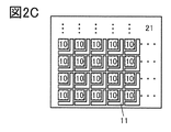
- 2A, 2B, and 2C are diagrams illustrating a pixel array.
- 3A, 3B, and 3C are diagrams illustrating a pixel circuit.
- 4A, 4B, and 4C are diagrams illustrating a pixel circuit.
- 5A, 5B, and 5C are diagrams illustrating a pixel circuit.
- 6A, 6B, and 6C are diagrams illustrating a pixel circuit.
- FIG. 7A is a diagram illustrating a rolling shutter system.
- FIG. 7B is a diagram illustrating the global shutter method.
- 8A and 8B are timing charts illustrating the operation of the pixel circuit.
- 9A and 9B are diagrams illustrating a pixel circuit.
- 10A is a diagram illustrating a configuration of a pixel of an imaging device.
- 10B and 10C are diagrams illustrating the configuration of the photoelectric conversion device.
- FIG. 10D is a diagram illustrating a configuration of a light emitting device.
- 11A and 11B are diagrams illustrating a configuration of a pixel of the imaging device.
- 12A, 12B, 12C, and 12D are diagrams illustrating a transistor.
- 13A, 13B, and 13C are perspective views of a package containing the imaging device.
- 14A, 14B, and 14C are diagrams illustrating electronic devices.
- the element may be configured by a plurality of elements unless there is a functional inconvenience.
- a plurality of transistors operating as switches may be connected in series or in parallel.
- a capacitor also referred to as a capacitor
- one conductor may have a plurality of functions such as a wiring, an electrode, and a terminal in some cases, and in this specification, a plurality of names may be used for the same element.
- a plurality of names may be used for the same element.
- the elements may actually be connected via a plurality of conductors. In this document, such a configuration is also included in the category of direct connection.
- One embodiment of the present invention is an imaging device including a light-emitting device (also referred to as a light-emitting element). Light is emitted from a light emitting device to a subject, and light reflected from the subject is received by a photoelectric conversion device (also referred to as a photoelectric conversion element) included in the pixel circuit. Since an EL element is used for the light emitting device, a thin imaging device with a light source can be formed.
- an element that emits infrared light as a light emitting device, it can be used for applications such as biometric authentication and failure analysis of industrial products.
- a pixel circuit which is easily applied to imaging by the global shutter method an image without distortion can be obtained even for a moving subject.
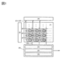
- FIG. 1 is a block diagram illustrating an imaging device of one embodiment of the present invention.
- the imaging device has a pixel array 21 having pixel circuits 10 arranged in a matrix, a circuit 22 (row driver) having a function of selecting a row of the pixel array 21, and a function of reading data from the pixel circuit 10.
- the circuit includes a circuit 23 and a circuit 28 for supplying a power supply potential.
- the light emitting device 11 is stacked on the pixel circuit 10.
- the circuit 23 includes a circuit 24 (column driver) having a function of selecting a column of the pixel array 21, a circuit 25 (CDS circuit) for performing correlated double sampling processing on output data of the pixel circuit 10, and a circuit A circuit 26 (A / D conversion circuit or the like) having a function of converting analog data output from the analog data 25 into digital data can be provided.
- a circuit 24 column driver
- CDS circuit circuit 25
- a circuit 26 A / D conversion circuit or the like
- the pixel circuit 10 and the light emitting device 11 may be configured not to overlap.
- the pixel circuits 10 and the light emitting devices 11 may be alternately arranged at regular intervals.
- the pixel circuits 10 and the light emitting devices 11 may be alternately arranged for each row. Note that the pixel circuits 10 and the light emitting devices 11 may be alternately arranged for each column.
- a configuration in which a light emitting device 11 is arranged between two adjacent pixel circuits 10 may be employed.
- the light emitting device 11 is arranged so as to have a region overlapping with a wiring connected to the pixel circuit 10. Therefore, in a broad sense, it can be said that the pixel circuit 10 and the light emitting device 11 overlap.
- 2C shows the same number of light emitting devices 11 as the pixel circuits 10, but the number of light emitting devices 11 may be different from that of the pixel circuits 10.
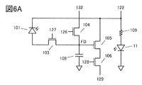
- FIG. 3A is a circuit diagram illustrating a pixel circuit 10 and a light-emitting device 11 that can be used for the imaging device of one embodiment of the present invention.
- the pixel circuit 10 can include a photoelectric conversion device 101, a transistor 103, a transistor 104, a transistor 105, a transistor 106, and a capacitor 108. Note that a structure without the capacitor 108 may be employed.
- One electrode (cathode) of the photoelectric conversion device 101 is electrically connected to one of a source and a drain of the transistor 103.
- the other of the source and the drain of the transistor 103 is electrically connected to one of the source and the drain of the transistor 104.
- One of a source and a drain of the transistor 104 is electrically connected to one electrode of the capacitor 108.
- One electrode of the capacitor 108 is electrically connected to the gate of the transistor 105.
- One of a source and a drain of the transistor 105 is electrically connected to one of a source and a drain of the transistor 106.
- a wiring that connects the other of the source and the drain of the transistor 103, one electrode of the capacitor 108, and the gate of the transistor 105 is referred to as a node FD.
- the node FD can function as a charge storage unit.
- the other electrode (anode) of the photoelectric conversion device 101 is electrically connected to the wiring 121.
- the gate of the transistor 103 is electrically connected to the wiring 127.
- the other of the source and the drain of the transistor 104 and the other of the source and the drain of the transistor 105 are electrically connected to a wiring 122.
- the gate of the transistor 104 is electrically connected to the wiring 126.
- the gate of the transistor 106 is electrically connected to the wiring 128.
- the other electrode of the capacitor 108 is electrically connected to a reference potential line such as a GND wiring, for example.
- the other of the source and the drain of the transistor 106 is electrically connected to the wiring 129.
- one electrode of the light emitting device 11 is electrically connected to the wiring 130.
- the other electrode of the light emitting device 11 is electrically connected to a reference potential line such as a GND wiring, for example.
- a reference potential line such as a GND wiring
- the wirings 127 and 128 can function as signal lines for controlling conduction of each transistor.
- the wiring 129 can function as an output line.
- the wirings 121, 122, and 130 can function as power supply lines.
- the cathode side of the photoelectric conversion device 101 is electrically connected to the transistor 103, and the node FD is reset to a high potential to operate. Is also a high potential).
- the wiring 130 has a function of supplying a potential for supplying a forward bias to the light emitting device 11 to emit light.
- FIG. 3B illustrates a configuration in which one electrode of the light-emitting device 11 is electrically connected to the wiring 122.
- the reset potential of the node FD, the power supply potential supplied to the transistor 105, and the input potential of the light-emitting device 11 can be shared, such a structure can be employed.
- a transistor 107 may be added to the structure of FIG. 3B.
- One of a source and a drain of the transistor 107 is electrically connected to one electrode of the light-emitting device 11.
- the other of the source and the drain of the transistor 107 is electrically connected to the wiring 122.
- the gate of the transistor 107 is electrically connected to the wiring 127.
- the resistance element 109 is connected between one electrode of the light emitting device 11 and the wiring 122 as shown in FIG. May be electrically connected.
- the resistance element 109 acts as a current limiting resistor, can limit the current flowing through the light emitting device 11, and can increase the reliability of the light emitting device 11.
- An appropriate value may be selected for the resistance value of the resistance element 109 in accordance with the electrical characteristics of the light emitting device 11.
- the transistor 107 shown in FIG. 3C may be operated instead of the resistor 109.
- the gate of the transistor 107 is electrically connected to the wiring 131. Therefore, by changing the potential of the wiring 131, the illuminance and the light emission timing of the light emitting device 11 can be arbitrarily controlled, and power consumption can be suppressed.
- the transistor 107 is provided.
- the other of the source and the drain of the transistor 107 is electrically connected to the wiring 130, and the gate of the transistor 107 is electrically connected to the wiring 127.
- It may be a configuration. In this structure, the input potential to the light emitting device 11 is controlled by the wiring 130, and the timing of light emission is controlled by the wiring 127.
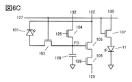
- FIGS. 4A to 4C show the structure in which the cathode of the photoelectric conversion device 101 is electrically connected to the node FD.
- the cathode of the photoelectric conversion device 101 may be electrically connected to the node FD.
- one electrode of the photoelectric conversion device 101 is electrically connected to the wiring 122, and the other electrode of the photoelectric conversion device 101 is connected to the source or the drain of the transistor 103. It is electrically connected to one. The other of the source and the drain of the transistor 104 is electrically connected to the wiring 132.
- the wiring 132 can function as a power supply line or a reset potential supply line. 5A to 5C and FIGS. 6A to 6C, the anode side of the photoelectric conversion device 101 is electrically connected to the transistor 103, and the node FD is reset to a low potential to operate.
- the wiring 132 has a low potential (a lower potential than the wiring 122).
- FIGS. 5A to 5C and FIGS. 6A to 6C can be referred to the description of FIGS. 3A to 3C and FIGS. 4A to 4C for the connection mode with the light emitting device 11 and its peripheral elements.
- a photodiode can be used as the photoelectric conversion device 101.
- imaging using infrared light is performed. Therefore, a photodiode capable of photoelectrically converting light in the infrared region is used for the photoelectric conversion device 101.
- a photodiode capable of photoelectrically converting light in the infrared region is used for the photoelectric conversion device 101.
- a pn junction photodiode using single crystal silicon for a photoelectric conversion portion a pin photodiode using polycrystalline silicon or microcrystalline silicon for a photoelectric conversion layer, or the like can be used.
- a material that can photoelectrically convert light in the infrared region such as a compound semiconductor, may be used.
- the transistor 103 has a function of controlling the potential of the node FD.
- the transistor 104 has a function of resetting the potential of the node FD.
- the transistor 105 functions as a source follower circuit and can output the potential of the node FD to the wiring 129 as image data.
- the transistor 106 has a function of selecting a pixel to output image data.
- a transistor including a metal oxide in a channel formation region (hereinafter, an OS transistor) is preferably used.
- the OS transistor has a characteristic of extremely low off-state current. With the use of the OS transistors as the transistors 103 and 104, the period during which charge can be held at the node FD can be extremely long. Therefore, it is possible to apply a global shutter method in which charge accumulation operation is simultaneously performed in all pixels without complicating a circuit configuration and an operation method.
- FIG. 7A is a diagram schematically illustrating the operation method of the rolling shutter system
- FIG. 7B is a diagram schematically illustrating the global shutter system.
- En represents the exposure (accumulation operation) of the n-th column (n is a natural number)
- Rn represents the read operation of the n-th column.
- 7A and 7B show the operation from the first row to the M-th row (M is a natural number).
- the rolling shutter method is an operation method of sequentially performing exposure and data reading, and is a method in which a reading period of a certain row and an exposure period of another row are overlapped. Since the reading operation is performed immediately after the exposure, imaging can be performed even with a circuit configuration in which the data retention period is relatively short. However, since an image of one frame is composed of data having no synchronization at the time of imaging, distortion occurs in imaging of a moving object.
- the global shutter method is an operation method in which exposure is performed simultaneously on all pixels, data is held in each pixel, and data is read out for each row. Therefore, an image without distortion can be obtained even when capturing a moving object.
- a transistor having a relatively high off-state current such as a transistor using Si (hereinafter referred to as a Si transistor) in a channel formation region
- Si transistor a transistor using Si
- a rolling shutter method is used because a data potential easily flows out of a charge storage portion.
- the global shutter method using Si transistors it is necessary to separately provide a memory circuit and the like, and further complicated operations must be performed at high speed.
- the OS transistor is used for the pixel circuit, the global shutter method can be easily realized because there is almost no outflow of the data potential from the charge storage portion.
- an OS transistor may be used as the transistors 105 and 106. Further, an OS transistor and a Si transistor may be arbitrarily combined and applied. Further, all the transistors may be OS transistors or Si transistors. Examples of the Si transistor include a transistor including amorphous silicon, a transistor including crystalline silicon (typically, low-temperature polysilicon, single crystal silicon, and the like).
- an EL element can be used.
- the EL element an element that emits infrared light can be used.
- an EL element which emits near-infrared light having a peak at a wavelength of 700 nm or more and 2500 nm or less is preferable.
- the position of a vein can be detected by receiving reflected light from a palm or a finger and forming an image. This effect can be used as biometric authentication.
- it can be used for nondestructive inspection such as inspection of foreign substances in food or failure analysis of industrial products using near infrared light having an appropriate wavelength.
- highly accurate sensing can be performed even if the subject moves.
- a thin imaging device with a light source can be realized, which can be easily mounted on various devices, and portability can be improved.
- the light emitting device 11 is in a state in which a power supply potential for appropriately emitting light is supplied to the light emitting device 11 at least during the accumulation operation.
- the transistor 104 is turned off and supply of a reset potential is cut off. Further, the potential of the node FD decreases in accordance with the operation of the photoelectric conversion device 101 (accumulation operation).
- the pixel circuits 10 shown in FIGS. 5A to 5C and 6A to 6C can be operated according to the timing chart of FIG. 8B. It is assumed that “H” is always supplied to the wiring 122 and “L” is always supplied to the wiring 132. The basic operation is the same as that described in the timing chart of FIG. 8A.
- a transistor may be provided with a back gate as illustrated in FIGS. 9A and 9B.
- FIG. 9A shows a configuration in which the back gate is electrically connected to the front gate, which has an effect of increasing the on-state current.
- FIG. 9B illustrates a structure in which the back gate is electrically connected to a wiring which can supply a constant potential, so that the threshold voltage of the transistor can be controlled.
- the pixel circuit may include a transistor without a back gate. Note that the structure in which the transistor is provided with a back gate can be applied to all the structures illustrated in FIGS. 3A to 3C, FIGS. 4A to 4C, FIGS. 5A to 5C, and FIGS. 6A to 6C.
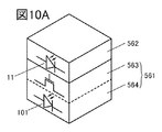
- FIG. 10A illustrates a structure of a pixel included in the imaging device.
- the pixel can have a stacked structure of a layer 561 including the pixel circuit 10 and a layer 562 including the light-emitting device 11.
- the layer 561 includes a layer 563 and a layer 564. Elements such as transistors included in the pixel circuit 10 are mainly provided in the layer 563.
- the layer 564 is mainly provided with the photoelectric conversion device 101.
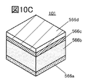
- the photoelectric conversion device 101 can be a stack of a layer 565a and a layer 565b as illustrated in FIG. 10B.
- the photoelectric conversion device 101 illustrated in FIG. 10B is a pn junction photodiode.
- a p-type semiconductor can be used for the layer 565a and an n-type semiconductor can be used for the layer 565b.
- an n-type semiconductor may be used for the layer 565a and a p-type semiconductor may be used for the layer 565b.
- the layer 566a may be an n-type semiconductor and the layer 566c may be a p-type semiconductor.
- the pn junction photodiode can be formed using single crystal silicon. Further, the pin junction photodiode can be formed using a thin film of single crystal silicon, microcrystalline silicon, polycrystalline silicon, or the like. Monocrystalline silicon, microcrystalline silicon, and polycrystalline silicon have sensitivity to infrared light and are suitable for detecting infrared light.
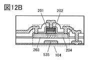
- a silicon substrate can be used as the layer 564 illustrated in FIG. 10A.
- the silicon substrate can include a Si transistor or the like in addition to the pn junction photodiode.
- a circuit for driving a pixel circuit, a circuit for reading an image signal, an image processing circuit, or the like can be provided using the Si transistor.
- part or all of the transistors described in Embodiment 1 and included in the peripheral circuits can be provided in the layer 564.
- the layer 564 may have a structure including a support having an insulating surface such as a glass substrate and the above-described pin junction photodiode.
- the layer 563 can include an OS transistor (for example, part or all of the transistors 103, 104, 105, 106, and 107 included in the pixel circuit 10). Further, some of the transistors included in the peripheral circuit described in Embodiment 1 may be included.
- the element and the peripheral circuit included in the pixel circuit can be dispersed in a plurality of layers and the element or the element and the peripheral circuit can be provided in an overlapping manner; thus, the area of the imaging device can be reduced. be able to.
- a metal oxide having an energy gap of 2 eV or more, preferably 2.5 eV or more, more preferably 3 eV or more can be used.
- an oxide semiconductor containing indium or the like is used.
- CAAC-OS CAC-Aligned Crystalline Oxide Semiconductor
- CAC-OS Cloud-Aligned Composite Oxide Semiconductor
- the CAAC-OS has stable atoms in its crystal and is suitable for a transistor or the like in which reliability is emphasized.
- the CAC-OS has high mobility characteristics, and thus is suitable for a transistor that drives at high speed or the like.
- the OS transistor has an extremely low off-current characteristic of several yA / ⁇ m (current value per 1 ⁇ m of channel width) because the energy gap of the semiconductor layer is large. Further, the OS transistor has characteristics different from those of the Si transistor, such as not generating impact ionization, avalanche breakdown, and a short-channel effect, and thus can form a highly reliable circuit with high withstand voltage. In addition, variation in electrical characteristics due to non-uniformity of crystallinity, which is a problem in the Si transistor, hardly occurs in the OS transistor.
- the semiconductor layer included in the OS transistor includes an In-M-Zn-based oxide including, for example, indium, zinc, and M (a metal such as aluminum, titanium, gallium, germanium, yttrium, zirconium, lanthanum, cerium, tin, neodymium, or hafnium). Can be obtained.
- the In-M-Zn-based oxide can be typically formed by a sputtering method. Alternatively, it may be formed by using an ALD (Atomic layer deposition) method.
- the atomic ratio of metal elements of a sputtering target used for forming the In-M-Zn-based oxide by a sputtering method satisfy In ⁇ M and Zn ⁇ M.
- each of the atomic ratios of the semiconductor layers to be formed includes a variation of ⁇ 40% of the atomic ratio of the metal element contained in the sputtering target.
- the semiconductor layer an oxide semiconductor with a low carrier density is used.
- the semiconductor layer has a carrier density of 1 ⁇ 10 17 / cm 3 or less, preferably 1 ⁇ 10 15 / cm 3 or less, further preferably 1 ⁇ 10 13 / cm 3 or less, more preferably 1 ⁇ 10 11 / cm 3. 3 or less, more preferably less than 1 ⁇ 10 10 / cm 3 , and an oxide semiconductor of 1 ⁇ 10 ⁇ 9 / cm 3 or more can be used.
- Such an oxide semiconductor is referred to as a high-purity intrinsic or substantially high-purity intrinsic oxide semiconductor. It can be said that the oxide semiconductor has a low density of defect states and has stable characteristics.
- this embodiment is not limited thereto, and an oxide semiconductor having an appropriate composition may be used depending on required semiconductor characteristics and electric characteristics (eg, field-effect mobility and threshold voltage) of the transistor.
- the carrier density and the impurity concentration of the semiconductor layer, the defect density, the atomic ratio between a metal element and oxygen, the interatomic distance, and the density be appropriate.
- the concentration of silicon or carbon (concentration obtained by secondary ion mass spectrometry (SIMS)) in the semiconductor layer is set to 2 ⁇ 10 18 atoms / cm 3 or less, preferably 2 ⁇ 10 17 atoms / cm 3 or less. / Cm 3 or less.
- an alkali metal and an alkaline earth metal may generate carriers when combined with an oxide semiconductor, which may increase off-state current of a transistor.
- concentration of the alkali metal or alkaline earth metal (concentration obtained by SIMS) in the semiconductor layer is set to 1 ⁇ 10 18 atoms / cm 3 or less, preferably 2 ⁇ 10 16 atoms / cm 3 or less.
- the nitrogen concentration (concentration obtained by SIMS) in the semiconductor layer is preferably 5 ⁇ 10 18 atoms / cm 3 or less.
- the transistor when hydrogen is contained in the oxide semiconductor included in the semiconductor layer, oxygen reacts with oxygen bonded to a metal atom to become water, which may cause oxygen vacancies in the oxide semiconductor.
- oxygen vacancy When an oxygen vacancy is contained in a channel formation region in an oxide semiconductor, the transistor might have normally-on characteristics. Further, a defect in which hydrogen is contained in an oxygen vacancy functions as a donor, and an electron serving as a carrier may be generated. Further, in some cases, part of hydrogen is bonded to oxygen which is bonded to a metal atom to generate electrons serving as carriers. Therefore, a transistor including an oxide semiconductor containing a large amount of hydrogen is likely to have normally-on characteristics.
- a defect in which hydrogen is contained in oxygen vacancies can function as a donor of an oxide semiconductor.
- the hydrogen concentration obtained by SIMS is lower than 1 ⁇ 10 20 atoms / cm 3 , preferably lower than 1 ⁇ 10 19 atoms / cm 3 , and more preferably lower than 5 ⁇ 10 18 atoms / cm 3. It is set to less than 3 , more preferably less than 1 ⁇ 10 18 atoms / cm 3 .
- an oxide semiconductor in which impurities such as hydrogen are sufficiently reduced is used for a channel formation region of a transistor, stable electric characteristics can be provided.
- the semiconductor layer may have a non-single-crystal structure, for example.
- the non-single-crystal structure includes, for example, a CAAC-OS having c-axis aligned crystals, a polycrystalline structure, a microcrystalline structure, or an amorphous structure.
- the amorphous structure has the highest density of defect states
- the CAAC-OS has the lowest density of defect states.
- An oxide semiconductor film having an amorphous structure has, for example, a disordered atomic arrangement and no crystalline component.
- an oxide film having an amorphous structure has, for example, a completely amorphous structure and no crystal part.
- the semiconductor layer is a mixed film including two or more of an amorphous structure region, a microcrystalline structure region, a polycrystalline structure region, a CAAC-OS region, and a single crystal structure region.
- the mixed film may have a single-layer structure or a stacked structure including any two or more of the above-described regions.
- CAC-OS which is one embodiment of a non-single-crystal semiconductor layer is described below.
- the CAC-OS is one structure of a material in which an element included in an oxide semiconductor is unevenly distributed in a size of, for example, 0.5 nm or more and 10 nm or less, preferably 1 nm or more and 2 nm or less.
- one or more metal elements are unevenly distributed in an oxide semiconductor, and a region including the metal element has a size of 0.5 nm to 10 nm, preferably 1 nm to 2 nm, or a size in the vicinity thereof.
- the state mixed by is also referred to as a mosaic shape or a patch shape.
- the oxide semiconductor preferably contains at least indium. In particular, it preferably contains indium and zinc. In addition to them, aluminum, gallium, yttrium, copper, vanadium, beryllium, boron, silicon, titanium, iron, nickel, germanium, zirconium, molybdenum, lanthanum, cerium, neodymium, hafnium, tantalum, tungsten, or magnesium, etc. Or a plurality of types selected from the group consisting of:
- CAC-OS in an In-Ga-Zn oxide is an indium oxide (hereinafter referred to as InO).
- InO indium oxide
- X1 X1 is greater real than 0
- X2 Zn Y2 O Z2 X2, Y2, and Z2 is larger real than 0
- gallium An oxide hereinafter, referred to as GaO X3 (X3 is a real number larger than 0)
- Ga X4 Zn Y4 O Z4 X4, Y4, and Z4 are real numbers larger than 0)
- the material becomes mosaic by separate into, mosaic InO X1 or in X2 Zn Y2 O Z2, is a configuration in which uniformly distributed in the film (hereinafter Also referred to as a cloud-like
- the CAC-OS is a composite oxide semiconductor having a structure in which a region containing GaO X3 as a main component and a region containing In X2 Zn Y2 O Z2 or InO X1 as a main component are mixed.
- the atomic ratio of In to the element M in the first region is larger than the atomic ratio of In to the element M in the second region.
- the In concentration is higher than that of the region No. 2.
- IGZO is a common name and may refer to one compound of In, Ga, Zn, and O. Representative examples are represented by InGaO 3 (ZnO) m1 (m1 is a natural number), or In (1 + x0) Ga ( 1-x0) O 3 (ZnO) m0 (-1 ⁇ x0 ⁇ 1, m0 is an arbitrary number) Crystalline compounds may be mentioned.
- the above crystalline compound has a single crystal structure, a polycrystal structure, or a CAAC structure.
- the CAAC structure is a crystal structure in which a plurality of IGZO nanocrystals have a c-axis orientation and are connected without being oriented in the ab plane.
- CAC-OS relates to the material configuration of an oxide semiconductor.
- a CAC-OS is a material composition containing In, Ga, Zn, and O, a region which is observed as a nanoparticle mainly containing Ga as a part, and a nanoparticle mainly containing In as a part.
- a region observed in a shape means a configuration in which each region is randomly dispersed in a mosaic shape. Therefore, in the CAC-OS, the crystal structure is a secondary element.
- the CAC-OS does not include a stacked structure of two or more kinds of films having different compositions.
- a structure including two layers of a film mainly containing In and a film mainly containing Ga is not included.
- the CAC-OS has a region which is observed in the form of a nanoparticle mainly including the metal element and a nanoparticle mainly including In as a part.
- the region observed in the form of particles refers to a configuration in which each of the regions is randomly dispersed in a mosaic shape.
- the CAC-OS can be formed by a sputtering method, for example, without intentionally heating the substrate.
- any one or more selected from an inert gas (typically, argon), an oxygen gas, and a nitrogen gas is used as a deposition gas.
- the flow rate ratio of the oxygen gas to the total flow rate of the film formation gas during the film formation is preferably as low as possible.
- the flow rate ratio of the oxygen gas is preferably from 0% to less than 30%, more preferably from 0% to 10%. .
- the CAC-OS is characterized in that a clear peak is not observed when measured using a ⁇ / 2 ⁇ scan by an Out-of-plane method, which is one of X-ray diffraction (XRD) measurement methods.
- XRD X-ray diffraction
- the CAC-OS includes, in an electron beam diffraction pattern obtained by irradiating an electron beam (also referred to as a nanobeam electron beam) with a probe diameter of 1 nm, a ring-shaped region (ring region) with high luminance and a ring-shaped region. Multiple bright spots are observed in the area. Therefore, the electron diffraction pattern shows that the crystal structure of the CAC-OS has an nc (nano-crystal) structure having no orientation in a planar direction and a cross-sectional direction.
- an electron beam also referred to as a nanobeam electron beam
- GaO X3 is a main component by EDX mapping acquired using energy dispersive X-ray spectroscopy (EDX). It can be confirmed that the region and the region containing In X2 Zn Y2 O Z2 or InO X1 as a main component are unevenly distributed and mixed.
- EDX energy dispersive X-ray spectroscopy
- the CAC-OS has a different structure from an IGZO compound in which metal elements are uniformly distributed, and has different properties from the IGZO compound.
- the CAC-OS is phase-separated into a region containing GaO X3 or the like as a main component and a region containing In X2 Zn Y2 O Z2 or InO X1 as a main component.
- the region in which In X2 Zn Y2 O Z2 or InO X1 is a main component is a region having higher conductivity than the region in which GaO X3 or the like is a main component. That is, the conductivity of the oxide semiconductor is exhibited by the flow of carriers in a region containing In X2 Zn Y2 O Z2 or InO X1 as a main component. Therefore, high field-effect mobility ( ⁇ ) can be realized by distributing a region containing In X2 Zn Y2 O Z2 or InO X1 as a main component in a cloud shape in the oxide semiconductor.
- a region containing GaO X3 or the like as a main component is a region having higher insulating properties as compared with a region containing In X2 Zn Y2 O Z2 or InO X1 as a main component. That is, a region in which GaO X3 or the like is a main component is distributed in the oxide semiconductor, whereby a leakage current can be suppressed and a favorable switching operation can be realized.
- the insulating property caused by GaO X3 or the like and the conductivity caused by In X2 Zn Y2 O Z2 or InO X1 act complementarily to each other, so that high performance is obtained.
- On-state current (I on ) and high field-effect mobility ( ⁇ ) can be realized.
- CAC-OS is suitable as a constituent material of various semiconductor devices.
- the layer 562 has the light emitting device 11.
- a light emitting device (EL element) using electroluminescence can be applied.
- An EL element has a layer containing a light-emitting compound (EL layer) between a pair of electrodes. When a potential difference larger than the threshold voltage of the EL element is generated between the pair of electrodes, holes are injected from the anode side into the EL layer and electrons are injected from the cathode side. The injected electrons and holes are recombined in the EL layer, and the light-emitting substance contained in the EL layer emits light.
- an organic EL element or an inorganic EL element can be used.
- an LED including a mini LED and a micro LED
- a compound semiconductor as a light emitting material
- an organic EL element by applying a voltage, electrons are injected from one electrode and holes are injected from the other electrode into the EL layer. Then, by recombination of the carriers (electrons and holes), the light-emitting organic compound forms an excited state and emits light when the excited state returns to the ground state. Due to such a mechanism, such a light-emitting device is called a current-excitation light-emitting device.
- the EL layer can be formed by a method such as an evaporation method (including a vacuum evaporation method), a transfer method, a printing method, an inkjet method, and a coating method.
- a method such as an evaporation method (including a vacuum evaporation method), a transfer method, a printing method, an inkjet method, and a coating method.
- the inorganic EL elements are classified according to their element structures into a dispersion-type inorganic EL element and a thin-film inorganic EL element.
- the dispersion-type inorganic EL element has a light-emitting layer in which particles of a light-emitting material are dispersed in a binder.
- the light-emission mechanism is donor-acceptor recombination light emission using a donor level and an acceptor level.
- the thin-film inorganic EL device has a structure in which a light-emitting layer is sandwiched between dielectric layers and further sandwiched between electrodes. The light-emitting mechanism is localized light emission using inner-shell electron transition of metal ions.
- FIG. 10D shows a configuration of the light emitting device 11.
- the EL layer 300 can include a plurality of layers such as a layer 330, a light-emitting layer 320, and a layer 340.
- the layer 330 can include, for example, a layer containing a substance having a high electron-injection property (an electron-injection layer), a layer containing a substance having a high electron-transport property (an electron-transport layer), or the like.
- the light-emitting layer 320 includes, for example, a light-emitting compound.
- the layer 340 can include, for example, a layer containing a substance having a high hole-injection property (a hole-injection layer) and a layer containing a substance having a high hole-transport property (a hole-transport layer).
- the EL layer 300 provided between the electrode 311 and the electrode 312 can function as a single light-emitting unit. Note that a plurality of light-emitting layers may be provided between the layer 330 and the layer 340. Note that the light emission direction is determined by using a light-transmitting conductive film for one of the electrode 311 and the electrode 312.
- the light emitting device 11 can emit light of various wavelengths depending on the material forming the EL layer 300.
- a material which emits light having a peak in near-infrared light (wavelength: 720 nm to 2500 nm) is used for a material of the EL layer 300.
- a material which emits light having a wavelength of 720 nm, 760 nm, 850 nm, 900 nm, or a wavelength near these wavelengths may be used depending on the application.
- the light-emitting material (also referred to as a guest material or a dopant material) of the EL layer 300 preferably includes an organometallic iridium complex that emits near-infrared light.
- the organometallic iridium complex preferably has a dimethylphenyl skeleton and a quinoxaline skeleton.
- organometallic iridium complex typically, bis ⁇ 4,6-dimethyl-2- [3- (3,5-dimethylphenyl) -2-quinoxalinyl- ⁇ N] phenyl- ⁇ C ⁇ (2, 2 ′, 6,6′-Tetramethyl-3,5-heptanedionato- ⁇ 2 O, O ′) iridium (III) (abbreviation: Ir (dmdpq) 2 (dpm)) or the like can be used.
- Ir (dmdpq) 2 (dpm) iridium
- an imaging element with high quantum efficiency or high luminous efficiency can be provided.
- a substance that is, a host material used to make the organometallic iridium complex in a dispersed state
- TPAQn 2,3-bis (4-diphenylaminophenyl) quinoxaline
- TPAQn 2,3-bis (4-diphenylaminophenyl) quinoxaline
- TPAQn 2,3-bis (4-diphenylaminophenyl) quinoxaline
- TPAQn 2,3-bis (4-diphenylaminophenyl) quinoxaline
- TPAQn 2,3-bis (4-diphenylaminophenyl) quinoxaline
- TPAQn 2,3-bis (4-diphenylaminophenyl) quinoxaline
- TPAQn 2,3-bis (4-diphenylaminophenyl) quinoxaline
- TPAQn 2,3-bis (4-diphenylaminophenyl) quinoxaline
- TPAQn 2,3-bis (4-diphenyla
- N- (1,1′-biphenyl-4-yl) -N- [4- (9-phenyl-9H- Carbazol-3-yl) phenyl] -9,9-dimethyl-9H-fluoren-2-amine (abbreviation: PCBBiF) is preferably used.
- the light-emitting layer 320 including the above-described organometallic iridium complex (guest material) and the above-described host material, near-infrared phosphorescence with high emission efficiency can be obtained from the EL layer 300. Can be.
- FIG. 11A is a diagram illustrating an example of a cross section of the pixel illustrated in FIG. 10A.
- the layer 564 has the pn junction photodiode illustrated in FIG. 10B as the photoelectric conversion device 101.
- the layer 563 includes an OS transistor, and FIG. 11A illustrates the transistors 103 and 107 with the structure illustrated in FIG. 3C as an example.
- the layer 565a can be a p-type region and the layer 565b can be an n-type region. Further, the wiring 121 having a function of a power supply line is connected to the layer 565b.
- FIG. 12A shows details of the OS transistor.
- the OS transistor illustrated in FIG. 12A has a self-aligned structure in which an insulating layer is provided over a stack of an oxide semiconductor layer and a conductive layer, and an opening which reaches the semiconductor layer is provided, so that the source electrode 205 and the drain electrode 206 are formed. It is.
- the OS transistor can include a channel formation region, a source region 203, and a drain region 204 formed in the oxide semiconductor layer 207, a gate electrode 201, and a gate insulating film 202. At least the gate insulating film 202 and the gate electrode 201 are provided in the opening.
- the oxide semiconductor layer 208 may be further provided in the opening.
- the OS transistor may have a self-aligned structure in which a source region 203 and a drain region 204 are formed in a semiconductor layer using the gate electrode 201 as a mask.
- a non-self-aligned top-gate transistor having a region where the source electrode 205 or the drain electrode 206 and the gate electrode 201 overlap with each other may be used.
- the transistors 103 and 107 have a structure including the back gate 535, a structure without a back gate may be employed.
- the back gate 535 may be electrically connected to a front gate of a transistor provided opposite to the transistor as illustrated in a cross-sectional view in the channel width direction of the transistor illustrated in FIG. 12D.
- FIG. 12D shows the transistor of FIG. 12A as an example, the same applies to transistors having other structures.
- a configuration in which a fixed potential different from that of the front gate may be supplied to the back gate 535 may be employed.
- An insulating layer 543 having a function of preventing diffusion of hydrogen is provided between a region where an OS transistor is formed and a region where a Si device such as the photoelectric conversion device 101 is formed. Hydrogen in the insulating layer provided near the photoelectric conversion device 101 terminates dangling bonds of silicon. On the other hand, hydrogen in the insulating layer provided in the vicinity of the channel formation regions of the transistors 103 and 107 is one of the factors which generate carriers in the oxide semiconductor layer.
- the reliability of the Si device can be improved by confining hydrogen in one layer. Further, by suppressing diffusion of hydrogen from one layer to the other layer, reliability of the OS transistor (the transistors 103 and 107) can be improved.
- the insulating layer 543 for example, aluminum oxide, aluminum oxynitride, gallium oxide, gallium oxynitride, yttrium oxide, yttrium oxynitride, hafnium oxide, hafnium oxynitride, yttria-stabilized zirconia (YSZ), or the like can be used.
- aluminum oxide, aluminum oxynitride, gallium oxide, gallium oxynitride, yttrium oxide, yttrium oxynitride, hafnium oxide, hafnium oxynitride, yttria-stabilized zirconia (YSZ), or the like can be used.
- planarization films 541 and 542 are provided over the transistors 103 and 107.
- the light emitting device 11 (the electrode 311, the EL layer 300, and the electrode 312) is provided on a surface in which uneven portions generated in a transistor and a contact portion are flattened by the flattening films 541 and 542.
- a low-resistance conductive film such as a metal can be used.
- the electrode 312 a light-transmitting conductive film which transmits near-infrared light can be used.
- the electrode 312 includes indium oxide containing tungsten oxide, indium zinc oxide containing tungsten oxide, indium oxide containing titanium oxide, indium tin oxide, indium tin oxide containing titanium oxide, and indium zinc oxide.
- a light-transmitting conductive material such as indium tin oxide to which silicon oxide is added can be used.
- the EL layer 300 overlapping with the electrodes 311 and 312 can emit light, but the EL layer 300 overlapping with the electrode 312 and not overlapping with the electrode 311 cannot emit light. Further, the EL layer 300 is an extremely thin thin film, and the absorption of near-infrared light can be ignored. Therefore, the EL layer 300 and the electrode 312 can be provided over the photoelectric conversion device 101.
- FIG. 11A illustrates a region where the photoelectric conversion device 101 and the transistor 103 overlap each other, this region is a part of the entire light receiving portion and does not significantly reduce light receiving ability. Note that a structure in which the photoelectric conversion device 101 and the transistor 103 do not have an overlapping region may be employed.
- light 601 is emitted from the light-emitting device 11 included in the layer 562 to the outside, and the reflected light 602 is received by the photoelectric conversion device 101 included in the layer 564 through the layers 562 and 563.
- a sealing layer 590 be provided between the light emitting device 11 and the substrate 580 to seal the light emitting device 11 so that oxygen, hydrogen, moisture, carbon dioxide, and the like do not enter the light emitting device 11.
- an ultraviolet curable resin or a thermosetting resin can be used, such as PVC (polyvinyl chloride), an acrylic resin, a polyimide, an epoxy resin, or a silicone resin. Resin, PVB (polyvinyl butyral) or EVA (ethylene vinyl acetate) can be used.
- a desiccant may be included in the sealing layer 590.
- a protective layer such as silicon nitride, silicon nitride oxide, aluminum oxide, aluminum nitride, aluminum oxynitride, aluminum nitride oxide, or DLC (Diamond Like Carbon) may be provided.
- FIG. 11B is a diagram illustrating an example of a cross section of a pixel when the pin junction photodiode illustrated in FIG. 10C is used as the photoelectric conversion device 101.
- the layer 566a can be a p-type region
- the layer 566b can be an i-type region
- the layer 566c can be an n-type region.
- the wiring 121 having a function of a power supply line is connected to the layer 566a.
- the photoelectric conversion device 101 and the wiring 121 are provided over a substrate 570.
- a substrate such as a glass substrate, a ceramics substrate, or a resin substrate having an insulating surface can be used.
- a metal substrate or a semiconductor substrate may be used as long as the surface has been subjected to an insulating treatment.
- the configuration of the imaging device with a light source can be used.
- FIG. 13A is an external perspective view of an upper surface side of a package containing an image sensor chip.
- the package includes a package substrate 410 for fixing the image sensor chip 450, a cover glass 420, an adhesive 430 for bonding the two, and the like.
- FIG. 13B is an external perspective view of the lower surface side of the package.
- a BGA Bit grid array
- BGA All grid array
- LGA Land Grid Array
- PGA Peripheral Component Interconnect
- FIG. 13C is a perspective view of the package illustrated with the cover glass 420 and a part of the adhesive 430 omitted.
- An electrode pad 460 is formed on the package substrate 410, and the electrode pad 460 and the bump 440 are electrically connected through a through hole.
- the electrode pad 460 is electrically connected to the image sensor chip 450 by a wire 470.
- the image sensor chip By mounting the image sensor chip in the above-described package, mounting on a printed circuit board or the like becomes easy, and the image sensor chip can be incorporated in various electronic devices.
- FIG. 14A illustrates a biometric authentication device, which includes a thin housing 911, operation buttons 912, a detection unit 913, and the like.
- the shape of a vein can be recognized by holding a hand or a finger over the detection unit 913 or by closely touching the detection unit 913.
- the acquired data can be transmitted to the server by the wireless communication unit 914 and collated with the database to identify an individual.
- a personal identification number or the like can be input using the operation buttons.
- the imaging device 915 according to one embodiment of the present invention is provided immediately below the detection portion, and does not require another light source; thus, a thin authentication device can be formed. By being thin, it can be easily incorporated into various devices. Also, portability is improved.
- FIG. 14B illustrates a nondestructive inspection device including a housing 921, an operation panel 922, a transport mechanism 923, a monitor 924, a detection unit 925, and the like.
- the inspected member 926 is transported by the transport mechanism 923 directly below the detection unit 925.
- the inspected member 926 is imaged by the imaging device 927 of one embodiment of the present invention provided in the detection unit 925, and the captured image is displayed on the monitor 924. After that, it is transported to the outlet of the housing 921, and the defective product is separated and collected.
- the imaging device 915 of one embodiment of the present invention does not require another light source, the detection unit 925 can be formed at low cost.
- FIG. 14C illustrates a food sorting device, which includes a housing 931, operation buttons 932, a display portion 933, a light-shielding hood 934, and the like.
- a food sorting device which includes a housing 931, operation buttons 932, a display portion 933, a light-shielding hood 934, and the like.
- the imaging device 935 of one embodiment of the present invention provided in the light receiving portion does not require another light source, a thin, lightweight, and portable food sorting device can be formed at low cost.
- the configuration shown in FIG. 14B may be used as a food sorting device.
- the configuration shown in FIG. 14C may be used as a non-destructive inspection device.
Abstract
Provided is a thin image-capture device having a light source. This image-capture device has a light-emitting device that emits infrared light, and the infrared light that is emitted by the light-emitting device and reflected from a subject is received by a photoelectric conversion device having a pixel circuit. Because an EL element is used for the light-emitting device, it is possible to configure a thin image-capture device with a light source. Also, by using a pixel circuit that uses an oxide semiconductor transistor having low off current characteristics, imaging using a global shutter method is possible, and even with a moving subject, it is possible to obtain an undistorted image.
Description
本発明の一態様は、撮像装置に関する。
One embodiment of the present invention relates to an imaging device.
なお、本発明の一態様は、上記の技術分野に限定されない。本明細書等で開示する発明の一態様の技術分野は、物、方法、または、製造方法に関するものである。または、本発明の一態様は、プロセス、マシン、マニュファクチャ、または、組成物(コンポジション・オブ・マター)に関するものである。そのため、より具体的に本明細書等で開示する本発明の一態様の技術分野としては、半導体装置、表示装置、液晶表示装置、発光装置、照明装置、蓄電装置、記憶装置、撮像装置、それらの駆動方法、または、それらの製造方法、を一例として挙げることができる。
Note that one embodiment of the present invention is not limited to the above technical field. The technical field of one embodiment of the present invention disclosed in this specification and the like relates to an object, a method, or a manufacturing method. Alternatively, one embodiment of the present invention relates to a process, a machine, a manufacturer, or a composition (composition of matter). Therefore, the technical field of one embodiment of the present invention disclosed in this specification and the like more specifically includes a semiconductor device, a display device, a liquid crystal display device, a light-emitting device, a lighting device, a power storage device, a storage device, an imaging device, Or the manufacturing method thereof can be cited as an example.
なお、本明細書等において半導体装置とは、半導体特性を利用することで機能しうる装置全般を指す。トランジスタ、半導体回路は半導体装置の一態様である。また、記憶装置、表示装置、撮像装置、電子機器は、半導体装置を有する場合がある。
Note that a semiconductor device in this specification and the like refers to any device that can function by utilizing semiconductor characteristics. A transistor and a semiconductor circuit are one embodiment of a semiconductor device. Further, the storage device, the display device, the imaging device, and the electronic device sometimes include a semiconductor device.
基板上に形成された酸化物半導体薄膜を用いてトランジスタを構成する技術が注目されている。例えば、酸化物半導体を有するオフ電流が極めて低いトランジスタを画素回路に用いる構成の撮像装置が特許文献1に開示されている。
Attention has been focused on a technique for forming a transistor using an oxide semiconductor thin film formed over a substrate. For example, Patent Document 1 discloses an imaging device in which a transistor including an oxide semiconductor and having extremely low off-state current is used for a pixel circuit.
撮像装置は、可視光を画像化する手段として用いられるだけでなく、様々な用途に用いられている。例えば、撮像装置は、個人認証、不良解析、医療診断、セキュリティ用途などに用いられている。これらの用途では、可視光の他、X線などの短波長の光、赤外線などの長波長の光などを用途に応じて使い分けている。
The imaging device is used not only as a means for imaging visible light but also for various uses. For example, an imaging device is used for personal authentication, failure analysis, medical diagnosis, security use, and the like. In these applications, in addition to visible light, short-wavelength light such as X-rays, long-wavelength light such as infrared light, and the like are properly used depending on the application.
可視光および赤外線としては自然光や室内光を利用する場合もあるが、専用の光源を用いることも一般化している。光源としては電球型のランプやLEDなどが多く用いられるが、撮像装置との組み合わせでは小型化、薄型化に課題がある。
Although natural light and indoor light may be used as visible light and infrared light, use of a dedicated light source is also common. As a light source, a bulb-type lamp, an LED, or the like is often used, but there is a problem in miniaturization and thinning in combination with an imaging device.
したがって、本発明の一態様では、光源を有する撮像装置を提供することを目的の一つとする。または、薄型の光源を有する撮像装置を提供することを目的の一つとする。または、薄型の光源を有し、当該光源から発する光の被写体からの反射光を撮像する撮像装置を提供することを目的の一つとする。または、薄型の赤外光源を有する撮像装置を提供することを目的の一つとする。
Therefore, it is an object of one embodiment of the present invention to provide an imaging device including a light source. Another object is to provide an imaging device having a thin light source. Alternatively, it is another object to provide an imaging device which includes a thin light source and captures reflected light from a subject of light emitted from the light source. Another object is to provide an imaging device having a thin infrared light source.
または、低消費電力の撮像装置を提供することを目的の一つとする。または、高速に撮像が行える撮像装置を提供することを目的の一つとする。または、信頼性の高い撮像装置を提供することを目的の一つとする。または、新規な撮像装置を提供することを目的の一つとする。または、上記撮像装置の動作方法を提供することを目的の一つとする。または、新規な半導体装置などを提供することを目的の一つとする。
Another object is to provide an imaging device with low power consumption. Another object is to provide an imaging device capable of high-speed imaging. Another object is to provide a highly reliable imaging device. Alternatively, it is another object to provide a novel imaging device. Another object is to provide an operation method of the imaging device. Another object is to provide a new semiconductor device or the like.
なお、これらの課題の記載は、他の課題の存在を妨げるものではない。なお、本発明の一態様は、これらの課題の全てを解決する必要はないものとする。なお、これら以外の課題は、明細書、図面、請求項などの記載から、自ずと明らかとなるものであり、明細書、図面、請求項などの記載から、これら以外の課題を抽出することが可能である。
Note that the description of these objects does not disturb the existence of other objects. Note that one embodiment of the present invention does not need to solve all of these problems. It should be noted that issues other than these are naturally evident from the description of the specification, drawings, claims, etc., and that other issues can be extracted from the description of the specifications, drawings, claims, etc. It is.
本発明の一態様は、光源を有する薄型の撮像装置に関する。
One embodiment of the present invention relates to a thin imaging device including a light source.
本発明の一態様は、第1の層と、第2の層と、を有する撮像装置であって、第1の層および第2の層は重なる領域を有し、第1の層は画素回路を有し、第2の層は発光デバイスを有し、画素回路は、光電変換デバイスと、トランジスタと、を有し、発光デバイスは、第1の電極と、第2の電極と、発光層と、を有し、発光層は、第1の電極と第2の電極との間に設けられ、光電変換デバイスは、第1の電極と重ならない領域を有する撮像装置である。
One embodiment of the present invention is an imaging device including a first layer and a second layer, wherein the first layer and the second layer have an overlapping region, and the first layer is a pixel circuit. A second layer has a light-emitting device, the pixel circuit has a photoelectric conversion device and a transistor, and the light-emitting device has a first electrode, a second electrode, and a light-emitting layer. , The light-emitting layer is provided between the first electrode and the second electrode, and the photoelectric conversion device is an imaging device having a region that does not overlap with the first electrode.
本発明の一態様の他の一態様は、第1の層と、第2の層と、を有する撮像装置であって、第1の層および第2の層は重なる領域を有し、第1の層は画素回路を有し、第2の層は発光デバイスを有し、発光デバイスは、第1の電極と、第2の電極と、発光層と、を有し、発光層は、第1の電極と第2の電極との間に設けられ、画素回路は、光電変換デバイスと、第1のトランジスタと、第2のトランジスタと、第3のトランジスタと、第4のトランジスタと、キャパシタと、を有し、光電変換デバイスの一方の電極は、第1のトランジスタのソースまたはドレインの一方と電気的に接続され、第1のトランジスタのソースまたはドレインの他方は、第2のトランジスタのソースまたはドレインの一方と電気的に接続され、第2のトランジスタのソースまたはドレインの一方は、キャパシタの一方の電極と電気的に接続され、キャパシタの一方の電極は、第3のトランジスタのゲートと電気的に接続され、第3のトランジスタのソースまたはドレインの一方は、第4のトランジスタのソースまたはドレインの一方と電気的に接続され、光電変換デバイスは、第1の電極と重ならない領域を有する撮像装置である。
Another embodiment of one embodiment of the present invention is an imaging device including a first layer and a second layer, wherein the first layer and the second layer have an overlapping region; Has a pixel circuit, the second layer has a light-emitting device, and the light-emitting device has a first electrode, a second electrode, and a light-emitting layer. And a pixel circuit provided between the first electrode and the second electrode, the pixel circuit includes a photoelectric conversion device, a first transistor, a second transistor, a third transistor, a fourth transistor, and a capacitor. And one electrode of the photoelectric conversion device is electrically connected to one of the source or the drain of the first transistor, and the other of the source or the drain of the first transistor is connected to the source or the drain of the second transistor. Is electrically connected to one of the second transistor One of the source and the drain is electrically connected to one electrode of the capacitor, the one electrode of the capacitor is electrically connected to the gate of the third transistor, and one of the source and the drain of the third transistor. Is electrically connected to one of a source and a drain of the fourth transistor, and the photoelectric conversion device is an imaging device having a region that does not overlap with the first electrode.
光電変換デバイスは、第2の電極および発光層と重なる領域を有していてもよい。
The photoelectric conversion device may have a region overlapping with the second electrode and the light-emitting layer.
発光デバイスには、赤外光を発する素子を用いることができる。また、第2の電極は、赤外光に透光性を有する透光性導電膜を用いることが好ましい。
An element that emits infrared light can be used for the light-emitting device. The second electrode is preferably formed using a light-transmitting conductive film having a property of transmitting infrared light.
第2のトランジスタのソースまたはドレインの他方と、第3のトランジスタのソースまたはドレインの他方は電気的に接続され、第3のトランジスタのソースまたはドレインの他方と、発光デバイスの一方の電極は電気的に接続することができる。
The other of the source and the drain of the second transistor is electrically connected to the other of the source and the drain of the third transistor. The other of the source and the drain of the third transistor and one electrode of the light-emitting device are electrically connected to each other. Can be connected to
上記と異なる構成として、光電変換デバイスの他方の電極と、第3のトランジスタのソースまたはドレインの他方は電気的に接続され、第3のトランジスタのソースまたはドレインの他方と、発光デバイスの一方の電極が電気的に接続されていてもよい。
As a different structure from the above, the other electrode of the photoelectric conversion device is electrically connected to the other of the source and the drain of the third transistor, and the other of the source and the drain of the third transistor is connected to the one of the electrodes of the light-emitting device. May be electrically connected.
上記2つの構成において、さらに第5のトランジスタを有し、第5のトランジスタのソースまたはドレインの一方は、発光デバイスの一方の電極と電気的に接続され、第5のトランジスタのソースまたはドレインの他方は、第3のトランジスタのソースまたはドレインの他方と電気的に接続されていてもよい。
In the above two structures, the semiconductor device further includes a fifth transistor, one of a source and a drain of the fifth transistor is electrically connected to one electrode of the light-emitting device, and the other of the source and the drain of the fifth transistor. May be electrically connected to the other of the source and the drain of the third transistor.
撮像装置が有するトランジスタの少なくとも一つ以上は、チャネル形成領域に金属酸化物を有し、金属酸化物は、Inと、Znと、M(MはAl、Ti、Ga、Sn、Y、Zr、La、Ce、NdまたはHf)と、を有することが好ましい。
At least one of the transistors included in the imaging device includes a metal oxide in a channel formation region. The metal oxide includes In, Zn, and M (M is Al, Ti, Ga, Sn, Y, Zr, La, Ce, Nd or Hf).
本発明の一態様を用いることで、光源を有する撮像装置を提供することができる。または、薄型の光源を有する撮像装置を提供することができる。または、薄型の光源を有し、当該光源から発する光の被写体からの反射光を撮像する撮像装置を提供することができる。または、薄型の赤外光源を有する撮像装置を提供することができる。
By using one embodiment of the present invention, an imaging device including a light source can be provided. Alternatively, an imaging device having a thin light source can be provided. Alternatively, an imaging device which has a thin light source and captures reflected light of a light emitted from the light source from a subject can be provided. Alternatively, an imaging device having a thin infrared light source can be provided.
または、低消費電力の撮像装置を提供することができる。または、高速に撮像が行える撮像装置を提供することができる。または、信頼性の高い撮像装置を提供することができる。または、新規な撮像装置を提供することができる。または、上記撮像装置の動作方法を提供することができる。または、新規な半導体装置などを提供することができる。
Alternatively, an imaging device with low power consumption can be provided. Alternatively, an imaging device which can perform imaging at high speed can be provided. Alternatively, a highly reliable imaging device can be provided. Alternatively, a novel imaging device can be provided. Alternatively, an operation method of the imaging device can be provided. Alternatively, a new semiconductor device or the like can be provided.
図1は、撮像装置を説明するブロック図である。
図2A、図2B、図2Cは、画素アレイを説明する図である。
図3A、図3B、図3Cは、画素回路を説明する図である。
図4A、図4B、図4Cは、画素回路を説明する図である。
図5A、図5B、図5Cは、画素回路を説明する図である。
図6A、図6B、図6Cは、画素回路を説明する図である。
図7Aは、ローリングシャッタ方式を説明する図である。図7Bは、グローバルシャッタ方式を説明する図である。
図8A、図8Bは、画素回路の動作を説明するタイミングチャートである。
図9A、図9Bは、画素回路を説明する図である。
図10Aは、撮像装置の画素の構成を説明する図である。図10B、図10Cは、光電変換デバイスの構成を説明する図である。図10Dは、発光デバイスの構成を説明する図である。
図11A、図11Bは、撮像装置の画素の構成を説明する図である。
図12A、図12B、図12C、図12Dは、トランジスタを説明する図である。
図13A、図13B、図13Cは、撮像装置を収めたパッケージの斜視図である。
図14A、図14B、図14Cは、電子機器を説明する図である。 FIG. 1 is a block diagram illustrating an imaging device.
2A, 2B, and 2C are diagrams illustrating a pixel array.
3A, 3B, and 3C are diagrams illustrating a pixel circuit.
4A, 4B, and 4C are diagrams illustrating a pixel circuit.
5A, 5B, and 5C are diagrams illustrating a pixel circuit.
6A, 6B, and 6C are diagrams illustrating a pixel circuit.
FIG. 7A is a diagram illustrating a rolling shutter system. FIG. 7B is a diagram illustrating the global shutter method.
8A and 8B are timing charts illustrating the operation of the pixel circuit.
9A and 9B are diagrams illustrating a pixel circuit.
FIG. 10A is a diagram illustrating a configuration of a pixel of an imaging device. 10B and 10C are diagrams illustrating the configuration of the photoelectric conversion device. FIG. 10D is a diagram illustrating a configuration of a light emitting device.
11A and 11B are diagrams illustrating a configuration of a pixel of the imaging device.
12A, 12B, 12C, and 12D are diagrams illustrating a transistor.
13A, 13B, and 13C are perspective views of a package containing the imaging device.
14A, 14B, and 14C are diagrams illustrating electronic devices.
実施の形態について、図面を用いて詳細に説明する。但し、本発明は以下の説明に限定されず、本発明の趣旨およびその範囲から逸脱することなくその形態および詳細を様々に変更し得ることは当業者であれば容易に理解される。したがって、本発明は以下に示す実施の形態の記載内容に限定して解釈されるものではない。なお、以下に説明する発明の構成において、同一部分または同様な機能を有する部分には同一の符号を異なる図面間で共通して用い、その繰り返しの説明は省略することがある。なお、図を構成する同じ要素のハッチングを異なる図面間で適宜省略または変更する場合もある。
Embodiments will be described in detail with reference to the drawings. However, the present invention is not limited to the following description, and it is easily understood by those skilled in the art that the form and details can be variously changed without departing from the spirit and scope of the present invention. Therefore, the present invention is not construed as being limited to the description of the embodiments below. Note that in the structures of the invention described below, the same portions or portions having similar functions are denoted by the same reference numerals in different drawings, and description thereof is not repeated in some cases. In addition, hatching of the same element configuring a drawing may be appropriately omitted or changed between different drawings.
また、回路図上では単一の要素として図示されている場合であっても、機能的に不都合がなければ、当該要素が複数で構成されてもよい。例えば、スイッチとして動作するトランジスタは、複数が直列または並列に接続されてもよい場合がある。また、キャパシタ(容量素子ともいう)を分割して複数の位置に配置してもよい場合がある。
Further, even if the element is illustrated as a single element on the circuit diagram, the element may be configured by a plurality of elements unless there is a functional inconvenience. For example, in some cases, a plurality of transistors operating as switches may be connected in series or in parallel. In some cases, a capacitor (also referred to as a capacitor) may be divided and arranged at a plurality of positions.
また、一つの導電体が、配線、電極および端子のような複数の機能を併せ持っている場合があり、本明細書においては、同一の要素に対して複数の呼称を用いる場合がある。また、回路図上で要素間が直接接続されているように図示されている場合であっても、実際には当該要素間が複数の導電体を介して接続されている場合があり、本明細書ではこのような構成でも直接接続の範疇に含める。
In addition, one conductor may have a plurality of functions such as a wiring, an electrode, and a terminal in some cases, and in this specification, a plurality of names may be used for the same element. Further, even though the elements are illustrated as being directly connected on the circuit diagram, the elements may actually be connected via a plurality of conductors. In this document, such a configuration is also included in the category of direct connection.
(実施の形態1)
本実施の形態では、本発明の一態様である撮像装置について、図面を参照して説明する。 (Embodiment 1)
In this embodiment, an imaging device which is one embodiment of the present invention will be described with reference to drawings.
本実施の形態では、本発明の一態様である撮像装置について、図面を参照して説明する。 (Embodiment 1)
In this embodiment, an imaging device which is one embodiment of the present invention will be described with reference to drawings.
本発明の一態様は、発光デバイス(発光素子ともいう)を有する撮像装置である。発光デバイスから被写体に光が照射され、被写体から反射された光を画素回路が有する光電変換デバイス(光電変換素子ともいう)で受光する。発光デバイスにはEL素子を用いるため、薄型の光源付撮像装置を構成することができる。
One embodiment of the present invention is an imaging device including a light-emitting device (also referred to as a light-emitting element). Light is emitted from a light emitting device to a subject, and light reflected from the subject is received by a photoelectric conversion device (also referred to as a photoelectric conversion element) included in the pixel circuit. Since an EL element is used for the light emitting device, a thin imaging device with a light source can be formed.
また、発光デバイスとして赤外光を発する素子を用いることで生体認証や工業製品の不良解析などの用途に用いることができる。また、グローバルシャッタ方式での撮像に適用しやすい画素回路を用いることで、動きのある被写体であっても歪のない画像を得ることができる。
In addition, by using an element that emits infrared light as a light emitting device, it can be used for applications such as biometric authentication and failure analysis of industrial products. In addition, by using a pixel circuit which is easily applied to imaging by the global shutter method, an image without distortion can be obtained even for a moving subject.
図1は、本発明の一態様の撮像装置を説明するブロック図である。当該撮像装置は、マトリクス状に配列された画素回路10を有する画素アレイ21と、画素アレイ21の行を選択する機能を有する回路22(ロードライバ)と、画素回路10からデータを読み出す機能を有する回路23と、電源電位を供給する回路28を有する。画素回路10上には、発光デバイス11が積層されている。
FIG. 1 is a block diagram illustrating an imaging device of one embodiment of the present invention. The imaging device has a pixel array 21 having pixel circuits 10 arranged in a matrix, a circuit 22 (row driver) having a function of selecting a row of the pixel array 21, and a function of reading data from the pixel circuit 10. The circuit includes a circuit 23 and a circuit 28 for supplying a power supply potential. The light emitting device 11 is stacked on the pixel circuit 10.
回路23は、画素アレイ21の列を選択する機能を有する回路24(カラムドライバ)と、画素回路10の出力データに対して相関二重サンプリング処理を行うための回路25(CDS回路)と、回路25から出力されたアナログデータをデジタルデータに変換する機能を有する回路26(A/D変換回路等)などを有することができる。
The circuit 23 includes a circuit 24 (column driver) having a function of selecting a column of the pixel array 21, a circuit 25 (CDS circuit) for performing correlated double sampling processing on output data of the pixel circuit 10, and a circuit A circuit 26 (A / D conversion circuit or the like) having a function of converting analog data output from the analog data 25 into digital data can be provided.
なお、解像度を重視しない場合は、画素回路10と発光デバイス11が重ならない構成としてもよい。例えば、図2Aに示すように、画素回路10と発光デバイス11とを一定の間隔で交互に配置してもよい。また、図2Bに示すように、画素回路10と発光デバイス11とを行毎に交互に配置してもよい。なお、画素回路10と発光デバイス11とを列毎に交互に配置してもよい。
If the resolution is not important, the pixel circuit 10 and the light emitting device 11 may be configured not to overlap. For example, as shown in FIG. 2A, the pixel circuits 10 and the light emitting devices 11 may be alternately arranged at regular intervals. Further, as shown in FIG. 2B, the pixel circuits 10 and the light emitting devices 11 may be alternately arranged for each row. Note that the pixel circuits 10 and the light emitting devices 11 may be alternately arranged for each column.
また、図2Cに示すように、隣り合う2つの画素回路10の間に発光デバイス11を配置する構成であってもよい。この場合、発光デバイス11は、画素回路10と接続する配線と重なる領域を有して配置される。したがって、広義では画素回路10と発光デバイス11が重なっているともいえる。なお、図2Cでは画素回路10と同数の発光デバイス11を図示しているが、発光デバイス11の数は画素回路10と異なっていてもよい。
Further, as shown in FIG. 2C, a configuration in which a light emitting device 11 is arranged between two adjacent pixel circuits 10 may be employed. In this case, the light emitting device 11 is arranged so as to have a region overlapping with a wiring connected to the pixel circuit 10. Therefore, in a broad sense, it can be said that the pixel circuit 10 and the light emitting device 11 overlap. 2C shows the same number of light emitting devices 11 as the pixel circuits 10, but the number of light emitting devices 11 may be different from that of the pixel circuits 10.
図3Aは、本発明の一態様の撮像装置に用いることができる画素回路10および発光デバイス11を説明する回路図である。画素回路10は、光電変換デバイス101と、トランジスタ103と、トランジスタ104と、トランジスタ105と、トランジスタ106と、キャパシタ108を有することができる。なお、キャパシタ108を設けない構成としてもよい。
FIG. 3A is a circuit diagram illustrating a pixel circuit 10 and a light-emitting device 11 that can be used for the imaging device of one embodiment of the present invention. The pixel circuit 10 can include a photoelectric conversion device 101, a transistor 103, a transistor 104, a transistor 105, a transistor 106, and a capacitor 108. Note that a structure without the capacitor 108 may be employed.
光電変換デバイス101の一方の電極(カソード)は、トランジスタ103のソースまたはドレインの一方と電気的に接続される。トランジスタ103のソースまたはドレインの他方は、トランジスタ104のソースまたはドレインの一方と電気的に接続される。トランジスタ104のソースまたはドレインの一方は、キャパシタ108の一方の電極と電気的に接続される。キャパシタ108の一方の電極は、トランジスタ105のゲートと電気的に接続される。トランジスタ105のソースまたはドレインの一方は、トランジスタ106のソースまたはドレインの一方と電気的に接続される。
One electrode (cathode) of the photoelectric conversion device 101 is electrically connected to one of a source and a drain of the transistor 103. The other of the source and the drain of the transistor 103 is electrically connected to one of the source and the drain of the transistor 104. One of a source and a drain of the transistor 104 is electrically connected to one electrode of the capacitor 108. One electrode of the capacitor 108 is electrically connected to the gate of the transistor 105. One of a source and a drain of the transistor 105 is electrically connected to one of a source and a drain of the transistor 106.
ここで、トランジスタ103のソースまたはドレインの他方、キャパシタ108の一方の電極、およびトランジスタ105のゲートを接続する配線をノードFDとする。ノードFDは、電荷蓄積部として機能させることができる。
Here, a wiring that connects the other of the source and the drain of the transistor 103, one electrode of the capacitor 108, and the gate of the transistor 105 is referred to as a node FD. The node FD can function as a charge storage unit.
光電変換デバイス101の他方の電極(アノード)は、配線121と電気的に接続される。トランジスタ103のゲートは、配線127と電気的に接続される。トランジスタ104のソースまたはドレインの他方およびトランジスタ105のソースまたはドレインの他方は、配線122に電気的に接続される。トランジスタ104のゲートは、配線126と電気的に接続される。トランジスタ106のゲートは、配線128と電気的に接続される。キャパシタ108の他方の電極は、例えばGND配線などの基準電位線と電気的に接続される。トランジスタ106のソースまたはドレインの他方は、配線129と電気的に接続される。
The other electrode (anode) of the photoelectric conversion device 101 is electrically connected to the wiring 121. The gate of the transistor 103 is electrically connected to the wiring 127. The other of the source and the drain of the transistor 104 and the other of the source and the drain of the transistor 105 are electrically connected to a wiring 122. The gate of the transistor 104 is electrically connected to the wiring 126. The gate of the transistor 106 is electrically connected to the wiring 128. The other electrode of the capacitor 108 is electrically connected to a reference potential line such as a GND wiring, for example. The other of the source and the drain of the transistor 106 is electrically connected to the wiring 129.
図3Aにおいて、発光デバイス11の一方の電極は、配線130と電気的に接続される。発光デバイス11の他方の電極は、例えばGND配線などの基準電位線と電気的に接続される。当該構成では、画素回路10と発光デバイス11との電気的な接続はないため、発光デバイス11に対する入力電位、および発光のタイミングは独立して制御することができる。
In FIG. 3A, one electrode of the light emitting device 11 is electrically connected to the wiring 130. The other electrode of the light emitting device 11 is electrically connected to a reference potential line such as a GND wiring, for example. In this configuration, since there is no electrical connection between the pixel circuit 10 and the light emitting device 11, the input potential to the light emitting device 11 and the timing of light emission can be controlled independently.
配線127、128は、各トランジスタの導通を制御する信号線として機能させることができる。配線129は出力線として機能させることができる。
The wirings 127 and 128 can function as signal lines for controlling conduction of each transistor. The wiring 129 can function as an output line.
配線121、122、130は、電源線としての機能を有することができる。図3Aに示す構成では光電変換デバイス101のカソード側がトランジスタ103と電気的に接続する構成であり、ノードFDを高電位にリセットして動作させる構成であるため、配線122は高電位(配線121よりも高い電位)とする。また、配線130は、発光デバイス11に順方向バイアスを供給して発光させるための電位を供給する機能を有する。
The wirings 121, 122, and 130 can function as power supply lines. In the configuration illustrated in FIG. 3A, the cathode side of the photoelectric conversion device 101 is electrically connected to the transistor 103, and the node FD is reset to a high potential to operate. Is also a high potential). In addition, the wiring 130 has a function of supplying a potential for supplying a forward bias to the light emitting device 11 to emit light.
図3Bは、発光デバイス11の一方の電極が配線122と電気的に接続された構成である。ノードFDのリセット電位、トランジスタ105に供給する電源電位、および発光デバイス11の入力電位を共通化できる場合は、当該構成とすることができる。
FIG. 3B illustrates a configuration in which one electrode of the light-emitting device 11 is electrically connected to the wiring 122. When the reset potential of the node FD, the power supply potential supplied to the transistor 105, and the input potential of the light-emitting device 11 can be shared, such a structure can be employed.
また、図3Cに示すように、図3Bの構成にトランジスタ107を加えてもよい。トランジスタ107のソースまたはドレインの一方は、発光デバイス11の一方の電極と電気的に接続される。トランジスタ107のソースまたはドレインの他方は、配線122と電気的に接続される。トランジスタ107のゲートは配線127と電気的に接続される。当該構成とすることによって、発光期間をトランジスタ103の導通の期間のみに制限することができ、消費電力を低減することができる。トランジスタ103の導通が必要な期間は、ノードFDに対するリセット動作期間および蓄積動作期間のみであり、読み出し動作期間などにおける不要な発光を抑えることができる。
Further, as shown in FIG. 3C, a transistor 107 may be added to the structure of FIG. 3B. One of a source and a drain of the transistor 107 is electrically connected to one electrode of the light-emitting device 11. The other of the source and the drain of the transistor 107 is electrically connected to the wiring 122. The gate of the transistor 107 is electrically connected to the wiring 127. With such a structure, the light emission period can be limited to only the period during which the transistor 103 is on, and power consumption can be reduced. The period in which the transistor 103 needs to be conductive is only the reset operation period and the accumulation operation period for the node FD, and unnecessary light emission in a read operation period or the like can be suppressed.
また、発光デバイス11に入力する適切な電位に対して、ノードFDのリセット電位などが高すぎる場合は、図4Aに示すように発光デバイス11の一方の電極と配線122との間に抵抗素子109を電気的に接続してもよい。抵抗素子109は電流制限抵抗として作用し、発光デバイス11に流れる電流を制限することができ、発光デバイス11の信頼性を高めることができる。抵抗素子109の抵抗値は、発光デバイス11の電気特性にあわせて適切な値を選択すればよい。
If the reset potential of the node FD is too high with respect to an appropriate potential input to the light emitting device 11, the resistance element 109 is connected between one electrode of the light emitting device 11 and the wiring 122 as shown in FIG. May be electrically connected. The resistance element 109 acts as a current limiting resistor, can limit the current flowing through the light emitting device 11, and can increase the reliability of the light emitting device 11. An appropriate value may be selected for the resistance value of the resistance element 109 in accordance with the electrical characteristics of the light emitting device 11.
なお、図4Bに示すように図3Cに示したトランジスタ107を抵抗素子109の代替えとして動作させてもよい。当該構成では、トランジスタ107のゲートは配線131と電気的に接続する。したがって、配線131の電位を変化させることで、発光デバイス11の照度および発光のタイミングを任意に制御することができ、消費電力を抑えることができる。
Note that as shown in FIG. 4B, the transistor 107 shown in FIG. 3C may be operated instead of the resistor 109. In this structure, the gate of the transistor 107 is electrically connected to the wiring 131. Therefore, by changing the potential of the wiring 131, the illuminance and the light emission timing of the light emitting device 11 can be arbitrarily controlled, and power consumption can be suppressed.
また、図4Cに示すように、トランジスタ107を設けた構成であって、トランジスタ107のソースまたはドレインの他方を配線130と電気的に接続し、トランジスタ107のゲートを配線127と電気的に接続する構成であってもよい。当該構成では、発光デバイス11に対する入力電位は配線130で制御し、発光のタイミングは配線127で制御する。
In addition, as illustrated in FIG. 4C, the transistor 107 is provided. The other of the source and the drain of the transistor 107 is electrically connected to the wiring 130, and the gate of the transistor 107 is electrically connected to the wiring 127. It may be a configuration. In this structure, the input potential to the light emitting device 11 is controlled by the wiring 130, and the timing of light emission is controlled by the wiring 127.
なお、図3A乃至図3Cおよび図4A乃至図4Cでは、光電変換デバイス101のカソードがノードFDと電気的に接続する構成を示したが、図5A乃至図5Cおよび図6A乃至図6Cに示すように光電変換デバイス101のアノードがノードFDと電気的に接続する構成としてもよい。
3A to 3C and FIGS. 4A to 4C show the structure in which the cathode of the photoelectric conversion device 101 is electrically connected to the node FD. However, as shown in FIGS. 5A to 5C and FIGS. 6A to 6C. Alternatively, the anode of the photoelectric conversion device 101 may be electrically connected to the node FD.
図5A乃至図5Cおよび図6A乃至図6Cに示す構成では、光電変換デバイス101の一方の電極が配線122と電気的に接続され、光電変換デバイス101の他方の電極がトランジスタ103のソースまたはドレインの一方と電気的に接続される。また、トランジスタ104のソースまたはドレインの他方が配線132と電気的に接続される。
In the structures illustrated in FIGS. 5A to 5C and FIGS. 6A to 6C, one electrode of the photoelectric conversion device 101 is electrically connected to the wiring 122, and the other electrode of the photoelectric conversion device 101 is connected to the source or the drain of the transistor 103. It is electrically connected to one. The other of the source and the drain of the transistor 104 is electrically connected to the wiring 132.
配線132は、電源線またはリセット電位の供給線としての機能を有することができる。図5A乃至図5Cおよび図6A乃至図6Cに示す構成では光電変換デバイス101のアノード側がトランジスタ103と電気的に接続する構成であり、ノードFDを低電位にリセットして動作させる構成であるため、配線132は低電位(配線122よりも低い電位)とする。
The wiring 132 can function as a power supply line or a reset potential supply line. 5A to 5C and FIGS. 6A to 6C, the anode side of the photoelectric conversion device 101 is electrically connected to the transistor 103, and the node FD is reset to a low potential to operate. The wiring 132 has a low potential (a lower potential than the wiring 122).
図5A乃至図5Cおよび図6A乃至図6Cに示す発光デバイス11およびその周辺要素との接続形態の説明は、図3A乃至図3Cおよび図4A乃至図4Cの説明を参照することができる。
5A to 5C and FIGS. 6A to 6C can be referred to the description of FIGS. 3A to 3C and FIGS. 4A to 4C for the connection mode with the light emitting device 11 and its peripheral elements.
光電変換デバイス101としては、フォトダイオードを用いることができる。本発明の一態様では、赤外線を用いた撮像を行う。したがって、光電変換デバイス101には、赤外領域の光を光電変換できるフォトダイオードを用いる。例えば、単結晶シリコンを光電変換部に用いたpn接合型フォトダイオード、多結晶シリコンまたは微結晶シリコンを光電変換層に用いたpin型フォトダイオードなどを用いることができる。または、化合物半導体など、赤外領域の光を光電変換できる材料を用いてもよい。
As the photoelectric conversion device 101, a photodiode can be used. In one embodiment of the present invention, imaging using infrared light is performed. Therefore, a photodiode capable of photoelectrically converting light in the infrared region is used for the photoelectric conversion device 101. For example, a pn junction photodiode using single crystal silicon for a photoelectric conversion portion, a pin photodiode using polycrystalline silicon or microcrystalline silicon for a photoelectric conversion layer, or the like can be used. Alternatively, a material that can photoelectrically convert light in the infrared region, such as a compound semiconductor, may be used.
トランジスタ103は、ノードFDの電位を制御する機能を有する。トランジスタ104は、ノードFDの電位をリセットする機能を有する。トランジスタ105はソースフォロア回路として機能し、ノードFDの電位を画像データとして配線129に出力することができる。トランジスタ106は、画像データを出力する画素を選択する機能を有する。
The transistor 103 has a function of controlling the potential of the node FD. The transistor 104 has a function of resetting the potential of the node FD. The transistor 105 functions as a source follower circuit and can output the potential of the node FD to the wiring 129 as image data. The transistor 106 has a function of selecting a pixel to output image data.
トランジスタ103およびトランジスタ104には、チャネル形成領域に金属酸化物を用いたトランジスタ(以下、OSトランジスタ)を用いることが好ましい。OSトランジスタは、オフ電流が極めて低い特性を有する。トランジスタ103、104にOSトランジスタを用いることによって、ノードFDで電荷を保持できる期間を極めて長くすることができる。そのため、回路構成や動作方法を複雑にすることなく、全画素で同時に電荷の蓄積動作を行うグローバルシャッタ方式を適用することができる。
As the transistors 103 and 104, a transistor including a metal oxide in a channel formation region (hereinafter, an OS transistor) is preferably used. The OS transistor has a characteristic of extremely low off-state current. With the use of the OS transistors as the transistors 103 and 104, the period during which charge can be held at the node FD can be extremely long. Therefore, it is possible to apply a global shutter method in which charge accumulation operation is simultaneously performed in all pixels without complicating a circuit configuration and an operation method.
図7Aはローリングシャッタ方式の動作方法を模式化した図であり、図7Bはグローバルシャッタ方式を模式化した図である。Enはn列目(nは自然数)の露光(蓄積動作)、Rnはn列目の読み出し動作を表している。図7A、図7Bでは、1行目からM行目(Mは自然数)までの動作を示している。
FIG. 7A is a diagram schematically illustrating the operation method of the rolling shutter system, and FIG. 7B is a diagram schematically illustrating the global shutter system. En represents the exposure (accumulation operation) of the n-th column (n is a natural number), and Rn represents the read operation of the n-th column. 7A and 7B show the operation from the first row to the M-th row (M is a natural number).
ローリングシャッタ方式は、露光とデータの読み出しを順次行う動作方法であり、ある行の読み出し期間と他の行の露光期間を重ねる方式である。露光後すぐに読み出し動作を行うため、データの保持期間が比較的短い回路構成であっても撮像を行うことができる。しかしながら、撮像の同時性がないデータで1フレームの画像が構成されるため、動体の撮像においては画像に歪が生じてしまう。
The rolling shutter method is an operation method of sequentially performing exposure and data reading, and is a method in which a reading period of a certain row and an exposure period of another row are overlapped. Since the reading operation is performed immediately after the exposure, imaging can be performed even with a circuit configuration in which the data retention period is relatively short. However, since an image of one frame is composed of data having no synchronization at the time of imaging, distortion occurs in imaging of a moving object.
一方で、グローバルシャッタ方式は、全画素で同時に露光を行って各画素にデータを保持し、行毎にデータを読み出す動作方法である。したがって、動体の撮像であっても歪のない画像を得ることができる。
On the other hand, the global shutter method is an operation method in which exposure is performed simultaneously on all pixels, data is held in each pixel, and data is read out for each row. Therefore, an image without distortion can be obtained even when capturing a moving object.
画素回路にチャネル形成領域にSiを用いたトランジスタ(以下、Siトランジスタ)などの比較的オフ電流の高いトランジスタを用いた場合は、電荷蓄積部からデータ電位が流出しやすいためローリングシャッタ方式が用いられる。Siトランジスタを用いてグローバルシャッタ方式を実現するには、別途メモリ回路などを設ける必要があり、さらに複雑な動作を高速で行わなければならない。一方で、画素回路にOSトランジスタを用いた場合は、電荷蓄積部からのデータ電位の流出がほとんどないため、容易にグローバルシャッタ方式を実現することができる。
In the case where a transistor having a relatively high off-state current, such as a transistor using Si (hereinafter referred to as a Si transistor) in a channel formation region, is used in a pixel circuit, a rolling shutter method is used because a data potential easily flows out of a charge storage portion. . In order to realize the global shutter method using Si transistors, it is necessary to separately provide a memory circuit and the like, and further complicated operations must be performed at high speed. On the other hand, when the OS transistor is used for the pixel circuit, the global shutter method can be easily realized because there is almost no outflow of the data potential from the charge storage portion.
なお、トランジスタ105、106にもOSトランジスタを適用してもよい。また、OSトランジスタおよびSiトランジスタを任意に組み合わせて適用してもよい。また、全てのトランジスタをOSトランジスタまたはSiトランジスタとしてもよい。Siトランジスタとしては、アモルファスシリコンを有するトランジスタ、結晶性のシリコン(代表的には、低温ポリシリコン、単結晶シリコンなど)を有するトランジスタなどが挙げられる。
Note that an OS transistor may be used as the transistors 105 and 106. Further, an OS transistor and a Si transistor may be arbitrarily combined and applied. Further, all the transistors may be OS transistors or Si transistors. Examples of the Si transistor include a transistor including amorphous silicon, a transistor including crystalline silicon (typically, low-temperature polysilicon, single crystal silicon, and the like).
発光デバイス11には、EL素子を用いることができる。当該EL素子としては、赤外光を発する素子を用いることができる。特に波長700nm以上2500nm以下にピークを有する近赤外光を発するEL素子であることが好ましい。例えば、波長760nmおよびその近傍の光は静脈中のヘモグロビンに吸収されやすいため、手のひらや指などからの反射光などを受光して画像化することで静脈の位置を検出することができる。当該作用は生体認証として利用することができる。また、適切な波長の近赤外光を利用して食品内の異物検査や工業製品の不良解析などの非破壊検査に利用することもできる。また、グローバルシャッタ方式と組み合わせることで、被写体に動きがあっても精度の高いセンシングが可能となる。
As the light emitting device 11, an EL element can be used. As the EL element, an element that emits infrared light can be used. In particular, an EL element which emits near-infrared light having a peak at a wavelength of 700 nm or more and 2500 nm or less is preferable. For example, since light having a wavelength of 760 nm and its vicinity is easily absorbed by hemoglobin in a vein, the position of a vein can be detected by receiving reflected light from a palm or a finger and forming an image. This effect can be used as biometric authentication. In addition, it can be used for nondestructive inspection such as inspection of foreign substances in food or failure analysis of industrial products using near infrared light having an appropriate wavelength. In addition, by combining with the global shutter method, highly accurate sensing can be performed even if the subject moves.
また、発光デバイス11としてEL素子を用いることで、薄型の光源付撮像装置を実現することができ、様々な機器へ搭載が容易となり、携帯性も向上させることができる。
Further, by using an EL element as the light emitting device 11, a thin imaging device with a light source can be realized, which can be easily mounted on various devices, and portability can be improved.
次に、図3A乃至図3Cおよび図4A乃至図4Cに示す画素回路10の動作の一例を図8Aのタイミングチャートを用いて説明する。なお、本明細書におけるタイミングチャートの説明においては、高電位を“H”、低電位を“L”で表す。配線121には常時“L”が供給され、配線122には常時“H”が供給されている状態とする。
Next, an example of the operation of the pixel circuit 10 illustrated in FIGS. 3A to 3C and FIGS. 4A to 4C will be described with reference to a timing chart of FIG. 8A. In the description of the timing chart in this specification, a high potential is represented by "H" and a low potential is represented by "L". It is assumed that “L” is always supplied to the wiring 121 and “H” is always supplied to the wiring 122.
なお、発光デバイス11においては、少なくとも蓄積動作の期間に適切に発光させるための電源電位が発光デバイス11に供給される状態とする。
Note that the light emitting device 11 is in a state in which a power supply potential for appropriately emitting light is supplied to the light emitting device 11 at least during the accumulation operation.
期間T1において、配線126の電位を“H”、配線127の電位を“H”、配線128の電位を“L”とすると、トランジスタ103、104が導通し、ノードFDには配線122の電位“H”が供給される(リセット動作)。
In the period T1, when the potential of the wiring 126 is “H”, the potential of the wiring 127 is “H”, and the potential of the wiring 128 is “L”, the transistors 103 and 104 are turned on, and the potential of the wiring 122 is connected to the node FD. H "is supplied (reset operation).
期間T2において、配線126の電位を“L”、配線127の電位を“H”、配線128の電位を“L”とすると、トランジスタ104が非導通となってリセット電位の供給が遮断される。また、光電変換デバイス101の動作に応じてノードFDの電位が低下する(蓄積動作)。
In the period T2, when the potential of the wiring 126 is “L”, the potential of the wiring 127 is “H”, and the potential of the wiring 128 is “L”, the transistor 104 is turned off and supply of a reset potential is cut off. Further, the potential of the node FD decreases in accordance with the operation of the photoelectric conversion device 101 (accumulation operation).
期間T3において、配線126の電位を“L”、配線127の電位を“L”、配線128の電位を“L”とすると、トランジスタ103が非導通となり、ノードFDの電位は確定し、保持される(保持動作)。このとき、ノードFDに接続されるトランジスタ103およびトランジスタ104にオフ電流の低いOSトランジスタを用いることによって、ノードFDからの不必要な電荷の流出を抑えることができ、データの保持時間の延ばすことができる。
In the period T3, when the potential of the wiring 126 is “L”, the potential of the wiring 127 is “L”, and the potential of the wiring 128 is “L”, the transistor 103 is turned off, and the potential of the node FD is determined and held. (Holding operation). At this time, by using an OS transistor with low off-state current for the transistor 103 and the transistor 104 connected to the node FD, unnecessary outflow of charge from the node FD can be suppressed and data retention time can be extended. it can.
期間T4において、配線126の電位を“L”、配線127の電位を“L”、配線128の電位を“H”とすると、トランジスタ106が導通し、トランジスタ105のソースフォロア動作によりノードFDの電位が配線129に読み出される(読み出し動作)。
In the period T4, when the potential of the wiring 126 is set to “L”, the potential of the wiring 127 is set to “L”, and the potential of the wiring 128 is set to “H”, the transistor 106 is turned on and the potential of the node FD is set by the source follower operation of the transistor 105. Is read to the wiring 129 (read operation).
以上が図3A乃至図3Cおよび図4A乃至図4Cに示す画素回路10の動作の一例である。
The above is an example of the operation of the pixel circuit 10 illustrated in FIGS. 3A to 3C and FIGS. 4A to 4C.
図5A乃至図5Cおよび図6A乃至図6Cに示す画素回路10は、図8Bのタイミングチャートに従って動作させることができる。なお、配線122には常時“H”が供給され、配線132には常時“L”が供給されている状態とする。基本的な動作は、上記の図8Aのタイミングチャートの説明と同様である。
The pixel circuits 10 shown in FIGS. 5A to 5C and 6A to 6C can be operated according to the timing chart of FIG. 8B. It is assumed that “H” is always supplied to the wiring 122 and “L” is always supplied to the wiring 132. The basic operation is the same as that described in the timing chart of FIG. 8A.
本発明の一態様においては、図9A、図9Bに例示するように、トランジスタにバックゲートを設けた構成としてもよい。図9Aは、バックゲートがフロントゲートと電気的に接続された構成を示しており、オン電流を高める効果を有する。図9Bは、バックゲートが定電位を供給できる配線と電気的に接続された構成を示しており、トランジスタのしきい値電圧を制御することができる。
In one embodiment of the present invention, a transistor may be provided with a back gate as illustrated in FIGS. 9A and 9B. FIG. 9A shows a configuration in which the back gate is electrically connected to the front gate, which has an effect of increasing the on-state current. FIG. 9B illustrates a structure in which the back gate is electrically connected to a wiring which can supply a constant potential, so that the threshold voltage of the transistor can be controlled.
また、図9A、図9Bを組み合わせるなど、それぞれのトランジスタが適切な動作が行えるような構成としてもよい。また、バックゲートが設けられないトランジスタを画素回路が有していてもよい。なお、トランジスタにバックゲートを設ける構成は、図3A乃至図3C、図4A乃至図4C、図5A乃至図5Cおよび図6A乃至図6Cに示す全ての構成に適用することができる。
9A and 9B may be combined so that each transistor can perform an appropriate operation. Further, the pixel circuit may include a transistor without a back gate. Note that the structure in which the transistor is provided with a back gate can be applied to all the structures illustrated in FIGS. 3A to 3C, FIGS. 4A to 4C, FIGS. 5A to 5C, and FIGS. 6A to 6C.
本実施の形態は、他の実施の形態の記載と適宜組み合わせることができる。
This embodiment can be combined with any of the other embodiments as appropriate.
(実施の形態2)
本実施の形態では、本発明の一態様の撮像装置の構造例などについて説明する。 (Embodiment 2)
In this embodiment, an example of a structure of an imaging device of one embodiment of the present invention and the like will be described.
本実施の形態では、本発明の一態様の撮像装置の構造例などについて説明する。 (Embodiment 2)
In this embodiment, an example of a structure of an imaging device of one embodiment of the present invention and the like will be described.
図10Aに、撮像装置が有する画素の構造を例示する。画素は、画素回路10を有する層561および発光デバイス11を有する層562の積層構造とすることができる。
FIG. 10A illustrates a structure of a pixel included in the imaging device. The pixel can have a stacked structure of a layer 561 including the pixel circuit 10 and a layer 562 including the light-emitting device 11.
層561は、層563および層564を有する。層563には、主に画素回路10が有するトランジスタ等の要素が設けられる。また、層564には、主に光電変換デバイス101が設けられる。光電変換デバイス101は、図10Bに示すように層565aと、層565bとの積層とすることができる。
The layer 561 includes a layer 563 and a layer 564. Elements such as transistors included in the pixel circuit 10 are mainly provided in the layer 563. The layer 564 is mainly provided with the photoelectric conversion device 101. The photoelectric conversion device 101 can be a stack of a layer 565a and a layer 565b as illustrated in FIG. 10B.
図10Bに示す光電変換デバイス101はpn接合型フォトダイオードであり、例えば、層565aにp型半導体、層565bにn型半導体を用いることができる。または、層565aにn型半導体、層565bにp型半導体を用いてもよい。
The photoelectric conversion device 101 illustrated in FIG. 10B is a pn junction photodiode. For example, a p-type semiconductor can be used for the layer 565a and an n-type semiconductor can be used for the layer 565b. Alternatively, an n-type semiconductor may be used for the layer 565a and a p-type semiconductor may be used for the layer 565b.
または、図10Cに示すようにpin接合型フォトダイオードであってもよい。例えば、層566aにp型半導体、層566bにi型半導体、層566cにn型半導体、層566dに透光性導電膜を用いることができる。または、層566aをn型半導体、層566cをp型半導体としてもよい。
Alternatively, it may be a pin junction type photodiode as shown in FIG. 10C. For example, a p-type semiconductor can be used for the layer 566a, an i-type semiconductor for the layer 566b, an n-type semiconductor for the layer 566c, and a light-transmitting conductive film for the layer 566d. Alternatively, the layer 566a may be an n-type semiconductor and the layer 566c may be a p-type semiconductor.
上記pn接合型フォトダイオードは、単結晶シリコンを用いて形成することができる。また、pin接合型フォトダイオードとしては、単結晶シリコン、微結晶シリコン、または多結晶シリコンなどの薄膜を用いて形成することもできる。単結晶シリコン、微結晶シリコン、多結晶シリコンは赤外光に感度を有し、赤外光の検知に適している。
The pn junction photodiode can be formed using single crystal silicon. Further, the pin junction photodiode can be formed using a thin film of single crystal silicon, microcrystalline silicon, polycrystalline silicon, or the like. Monocrystalline silicon, microcrystalline silicon, and polycrystalline silicon have sensitivity to infrared light and are suitable for detecting infrared light.
図10Aに示す層564としては、例えばシリコン基板を用いることができる。当該シリコン基板は、pn接合型フォトダイオードの他にSiトランジスタ等を有することができる。当該Siトランジスタを用いて、画素回路を駆動する回路、画像信号の読み出し回路、画像処理回路等を設けることができる。具体的には、実施の形態1で説明し周辺回路(画素回路10、回路22、23、28など)が有する一部または全てのトランジスタを層564に設けることができる。
As the layer 564 illustrated in FIG. 10A, for example, a silicon substrate can be used. The silicon substrate can include a Si transistor or the like in addition to the pn junction photodiode. A circuit for driving a pixel circuit, a circuit for reading an image signal, an image processing circuit, or the like can be provided using the Si transistor. Specifically, part or all of the transistors described in Embodiment 1 and included in the peripheral circuits (the pixel circuit 10, the circuits 22, 23,, and the like) can be provided in the layer 564.
または、層564は、ガラス基板などの絶縁性の表面を有する支持体および上述したpin接合型フォトダイオードを有する構成であってもよい。
Alternatively, the layer 564 may have a structure including a support having an insulating surface such as a glass substrate and the above-described pin junction photodiode.
層563は、OSトランジスタ(例えば、画素回路10が有するトランジスタ103、104、105、106、107の一部または全て)を有することができる。また、実施の形態1で説明した周辺回路が有する一部のトランジスタを有していてもよい。
The layer 563 can include an OS transistor (for example, part or all of the transistors 103, 104, 105, 106, and 107 included in the pixel circuit 10). Further, some of the transistors included in the peripheral circuit described in Embodiment 1 may be included.
当該構成とすることで、画素回路を構成する要素および周辺回路を複数の層に分散させ、当該要素同士または当該要素と当該周辺回路を重ねて設けることができるため、撮像装置の面積を小さくすることができる。
With such a structure, the element and the peripheral circuit included in the pixel circuit can be dispersed in a plurality of layers and the element or the element and the peripheral circuit can be provided in an overlapping manner; thus, the area of the imaging device can be reduced. be able to.
OSトランジスタに用いる半導体材料としては、エネルギーギャップが2eV以上、好ましくは2.5eV以上、より好ましくは3eV以上である金属酸化物を用いることができる。代表的には、インジウムを含む酸化物半導体などであり、例えば、後述するC−Axis Aligned Crystalline Oxide Semiconductor(CAAC−OS)またはCloud−Aligned Composite Oxide Semiconductor(CAC−OS)などを用いることができる。CAAC−OSは結晶を構成する原子が安定であり、信頼性を重視するトランジスタなどに適する。また、CAC−OSは、高移動度特性を示すため、高速駆動を行うトランジスタなどに適する。
As a semiconductor material used for the OS transistor, a metal oxide having an energy gap of 2 eV or more, preferably 2.5 eV or more, more preferably 3 eV or more can be used. Typically, an oxide semiconductor containing indium or the like is used. For example, CAC-Aligned Crystalline Oxide Semiconductor (CAAC-OS) or Cloud-Aligned Composite Oxide Semiconductor, which can be described later, is used (CAC-OS). The CAAC-OS has stable atoms in its crystal and is suitable for a transistor or the like in which reliability is emphasized. In addition, the CAC-OS has high mobility characteristics, and thus is suitable for a transistor that drives at high speed or the like.
OSトランジスタは半導体層のエネルギーギャップが大きいため、数yA/μm(チャネル幅1μmあたりの電流値)という極めて低いオフ電流特性を示す。また、OSトランジスタは、インパクトイオン化、アバランシェ降伏、および短チャネル効果などが生じないなどSiトランジスタとは異なる特徴を有し、高耐圧で信頼性の高い回路を形成することができる。また、Siトランジスタでは問題となる結晶性の不均一性に起因する電気特性のばらつきもOSトランジスタでは生じにくい。
The OS transistor has an extremely low off-current characteristic of several yA / μm (current value per 1 μm of channel width) because the energy gap of the semiconductor layer is large. Further, the OS transistor has characteristics different from those of the Si transistor, such as not generating impact ionization, avalanche breakdown, and a short-channel effect, and thus can form a highly reliable circuit with high withstand voltage. In addition, variation in electrical characteristics due to non-uniformity of crystallinity, which is a problem in the Si transistor, hardly occurs in the OS transistor.
OSトランジスタが有する半導体層は、例えばインジウム、亜鉛およびM(アルミニウム、チタン、ガリウム、ゲルマニウム、イットリウム、ジルコニウム、ランタン、セリウム、スズ、ネオジムまたはハフニウム等の金属)を含むIn−M−Zn系酸化物で表記される膜とすることができる。In−M−Zn系酸化物は代表的には、スパッタリング法で形成することができる。または、ALD(Atomic layer deposition)法を用いて形成してもよい。
The semiconductor layer included in the OS transistor includes an In-M-Zn-based oxide including, for example, indium, zinc, and M (a metal such as aluminum, titanium, gallium, germanium, yttrium, zirconium, lanthanum, cerium, tin, neodymium, or hafnium). Can be obtained. The In-M-Zn-based oxide can be typically formed by a sputtering method. Alternatively, it may be formed by using an ALD (Atomic layer deposition) method.
In−M−Zn系酸化物をスパッタリング法で形成するために用いるスパッタリングターゲットの金属元素の原子数比は、In≧M、Zn≧Mを満たすことが好ましい。このようなスパッタリングターゲットの金属元素の原子数比として、In:M:Zn=1:1:1、In:M:Zn=1:1:1.2、In:M:Zn=3:1:2、In:M:Zn=4:2:3、In:M:Zn=4:2:4.1、In:M:Zn=5:1:6、In:M:Zn=5:1:7、In:M:Zn=5:1:8等が好ましい。なお、成膜される半導体層の原子数比はそれぞれ、上記のスパッタリングターゲットに含まれる金属元素の原子数比のプラスマイナス40%の変動を含む。
It is preferable that the atomic ratio of metal elements of a sputtering target used for forming the In-M-Zn-based oxide by a sputtering method satisfy In ≧ M and Zn ≧ M. As the atomic ratio of metal elements of such a sputtering target, In: M: Zn = 1: 1: 1, In: M: Zn = 1: 1: 1.2, In: M: Zn = 3: 1: 2, In: M: Zn = 4: 2: 3, In: M: Zn = 4: 2: 4.1, In: M: Zn = 5: 1: 6, In: M: Zn = 5: 1: 7, In: M: Zn = 5: 1: 8 and the like are preferable. Note that each of the atomic ratios of the semiconductor layers to be formed includes a variation of ± 40% of the atomic ratio of the metal element contained in the sputtering target.
半導体層としては、キャリア密度の低い酸化物半導体を用いる。例えば、半導体層は、キャリア密度が1×10¹⁷/cm3以下、好ましくは1×1015/cm3以下、さらに好ましくは1×1013/cm3以下、より好ましくは1×1011/cm3以下、さらに好ましくは1×1010/cm3未満であり、1×10−9/cm3以上の酸化物半導体を用いることができる。そのような酸化物半導体を、高純度真性または実質的に高純度真性な酸化物半導体と呼ぶ。当該酸化物半導体は欠陥準位密度が低く、安定な特性を有する酸化物半導体であるといえる。
As the semiconductor layer, an oxide semiconductor with a low carrier density is used. For example, the semiconductor layer has a carrier density of 1 × 10 17 / cm 3 or less, preferably 1 × 10 15 / cm 3 or less, further preferably 1 × 10 13 / cm 3 or less, more preferably 1 × 10 11 / cm 3. 3 or less, more preferably less than 1 × 10 10 / cm 3 , and an oxide semiconductor of 1 × 10 −9 / cm 3 or more can be used. Such an oxide semiconductor is referred to as a high-purity intrinsic or substantially high-purity intrinsic oxide semiconductor. It can be said that the oxide semiconductor has a low density of defect states and has stable characteristics.
なお、これらに限られず、必要とするトランジスタの半導体特性および電気特性(電界効果移動度、しきい値電圧等)に応じて適切な組成の酸化物半導体を用いればよい。また、必要とするトランジスタの半導体特性を得るために、半導体層のキャリア密度や不純物濃度、欠陥密度、金属元素と酸素の原子数比、原子間距離、密度等を適切なものとすることが好ましい。
Note that this embodiment is not limited thereto, and an oxide semiconductor having an appropriate composition may be used depending on required semiconductor characteristics and electric characteristics (eg, field-effect mobility and threshold voltage) of the transistor. In addition, in order to obtain necessary semiconductor characteristics of a transistor, it is preferable that the carrier density and the impurity concentration of the semiconductor layer, the defect density, the atomic ratio between a metal element and oxygen, the interatomic distance, and the density be appropriate. .
半導体層を構成する酸化物半導体において、第14族元素の一つであるシリコンや炭素が含まれると、酸素欠損が増加し、n型化してしまう。このため、半導体層におけるシリコンや炭素の濃度(二次イオン質量分析法(SIMS:Secondary Ion Mass Spectrometry)により得られる濃度)を、2×10¹⁸atoms/cm3以下、好ましくは2×1017atoms/cm3以下とする。
When an oxide semiconductor included in the semiconductor layer contains silicon or carbon, which is one of Group 14 elements, oxygen vacancies increase and the semiconductor becomes n-type. For this reason, the concentration of silicon or carbon (concentration obtained by secondary ion mass spectrometry (SIMS)) in the semiconductor layer is set to 2 × 10 18 atoms / cm 3 or less, preferably 2 × 10 17 atoms / cm 3 or less. / Cm 3 or less.
また、アルカリ金属およびアルカリ土類金属は、酸化物半導体と結合するとキャリアを生成する場合があり、トランジスタのオフ電流が増大してしまうことがある。このため、半導体層におけるアルカリ金属またはアルカリ土類金属の濃度(SIMSにより得られる濃度)を、1×10¹⁸atoms/cm3以下、好ましくは2×1016atoms/cm3以下にする。
In addition, an alkali metal and an alkaline earth metal may generate carriers when combined with an oxide semiconductor, which may increase off-state current of a transistor. For this reason, the concentration of the alkali metal or alkaline earth metal (concentration obtained by SIMS) in the semiconductor layer is set to 1 × 10 18 atoms / cm 3 or less, preferably 2 × 10 16 atoms / cm 3 or less.
また、半導体層を構成する酸化物半導体に窒素が含まれていると、キャリアである電子が生じてキャリア密度が増加し、n型化しやすい。この結果、窒素が含まれている酸化物半導体を用いたトランジスタはノーマリーオン特性となりやすい。このため半導体層における窒素濃度(SIMSにより得られる濃度)は、5×10¹⁸atoms/cm3以下にすることが好ましい。
In addition, when nitrogen is contained in the oxide semiconductor included in the semiconductor layer, electrons serving as carriers are generated, the carrier density is increased, and the oxide semiconductor is easily made n-type. As a result, a transistor including an oxide semiconductor containing nitrogen is likely to have normally-on characteristics. Therefore, the nitrogen concentration (concentration obtained by SIMS) in the semiconductor layer is preferably 5 × 10 18 atoms / cm 3 or less.
また、半導体層を構成する酸化物半導体に水素が含まれていると、金属原子と結合する酸素と反応して水になるため、酸化物半導体中に酸素欠損を形成する場合がある。酸化物半導体中のチャネル形成領域に酸素欠損が含まれていると、トランジスタはノーマリーオン特性となる場合がある。さらに、酸素欠損に水素が入った欠陥はドナーとして機能し、キャリアである電子が生成されることがある。また、水素の一部が金属原子と結合する酸素と結合して、キャリアである電子を生成する場合がある。したがって、水素が多く含まれている酸化物半導体を用いたトランジスタは、ノーマリーオン特性となりやすい。
In addition, when hydrogen is contained in the oxide semiconductor included in the semiconductor layer, oxygen reacts with oxygen bonded to a metal atom to become water, which may cause oxygen vacancies in the oxide semiconductor. When an oxygen vacancy is contained in a channel formation region in an oxide semiconductor, the transistor might have normally-on characteristics. Further, a defect in which hydrogen is contained in an oxygen vacancy functions as a donor, and an electron serving as a carrier may be generated. Further, in some cases, part of hydrogen is bonded to oxygen which is bonded to a metal atom to generate electrons serving as carriers. Therefore, a transistor including an oxide semiconductor containing a large amount of hydrogen is likely to have normally-on characteristics.
酸素欠損に水素が入った欠陥は、酸化物半導体のドナーとして機能しうる。しかしながら、当該欠陥を定量的に評価することは困難である。そこで、酸化物半導体においては、ドナー濃度ではなく、キャリア濃度で評価される場合がある。よって、本明細書等では、酸化物半導体のパラメータとして、ドナー濃度ではなく、電界が印加されない状態を想定したキャリア濃度を用いる場合がある。つまり、本明細書等に記載の「キャリア濃度」は、「ドナー濃度」と言い換えることができる場合がある。
A defect in which hydrogen is contained in oxygen vacancies can function as a donor of an oxide semiconductor. However, it is difficult to quantitatively evaluate the defect. Therefore, in some cases, an oxide semiconductor is evaluated not by a donor concentration but by a carrier concentration. Therefore, in this specification and the like, a carrier concentration which assumes a state where an electric field is not applied is used instead of a donor concentration as a parameter of an oxide semiconductor in some cases. That is, the “carrier concentration” described in this specification and the like may be referred to as the “donor concentration” in some cases.
よって、酸化物半導体中の水素はできる限り低減されていることが好ましい。具体的には、酸化物半導体において、SIMSにより得られる水素濃度を、1×10²⁰atoms/cm3未満、好ましくは1×1019atoms/cm3未満、より好ましくは5×1018atoms/cm3未満、さらに好ましくは1×1018atoms/cm3未満とする。水素などの不純物が十分に低減された酸化物半導体をトランジスタのチャネル形成領域に用いることで、安定した電気特性を付与することができる。
Therefore, it is preferable that hydrogen in the oxide semiconductor be reduced as much as possible. Specifically, in the oxide semiconductor, the hydrogen concentration obtained by SIMS is lower than 1 × 10 20 atoms / cm 3 , preferably lower than 1 × 10 19 atoms / cm 3 , and more preferably lower than 5 × 10 18 atoms / cm 3. It is set to less than 3 , more preferably less than 1 × 10 18 atoms / cm 3 . When an oxide semiconductor in which impurities such as hydrogen are sufficiently reduced is used for a channel formation region of a transistor, stable electric characteristics can be provided.
また、半導体層は、例えば非単結晶構造でもよい。非単結晶構造は、例えば、c軸に配向した結晶を有するCAAC−OS、多結晶構造、微結晶構造、または非晶質構造を含む。非単結晶構造において、非晶質構造は最も欠陥準位密度が高く、CAAC−OSは最も欠陥準位密度が低い。
Further, the semiconductor layer may have a non-single-crystal structure, for example. The non-single-crystal structure includes, for example, a CAAC-OS having c-axis aligned crystals, a polycrystalline structure, a microcrystalline structure, or an amorphous structure. Among the non-single-crystal structures, the amorphous structure has the highest density of defect states, and the CAAC-OS has the lowest density of defect states.
非晶質構造の酸化物半導体膜は、例えば、原子配列が無秩序であり、結晶成分を有さない。または、非晶質構造の酸化物膜は、例えば、完全な非晶質構造であり、結晶部を有さない。
An oxide semiconductor film having an amorphous structure has, for example, a disordered atomic arrangement and no crystalline component. Alternatively, an oxide film having an amorphous structure has, for example, a completely amorphous structure and no crystal part.
なお、半導体層が、非晶質構造の領域、微結晶構造の領域、多結晶構造の領域、CAAC−OSの領域、単結晶構造の領域のうち、二種以上を有する混合膜であってもよい。混合膜は、例えば上述した領域のうち、いずれか二種以上の領域を含む単層構造、または積層構造を有する場合がある。
Note that even when the semiconductor layer is a mixed film including two or more of an amorphous structure region, a microcrystalline structure region, a polycrystalline structure region, a CAAC-OS region, and a single crystal structure region. Good. For example, the mixed film may have a single-layer structure or a stacked structure including any two or more of the above-described regions.
以下では、非単結晶の半導体層の一態様であるCAC−OSの構成について説明する。
The structure of a CAC-OS which is one embodiment of a non-single-crystal semiconductor layer is described below.
CAC−OSとは、例えば、酸化物半導体を構成する元素が、0.5nm以上10nm以下、好ましくは、1nm以上2nm以下、またはその近傍のサイズで偏在した材料の一構成である。なお、以下では、酸化物半導体において、一つあるいはそれ以上の金属元素が偏在し、該金属元素を有する領域が、0.5nm以上10nm以下、好ましくは、1nm以上2nm以下、またはその近傍のサイズで混合した状態をモザイク状、またはパッチ状ともいう。
The CAC-OS is one structure of a material in which an element included in an oxide semiconductor is unevenly distributed in a size of, for example, 0.5 nm or more and 10 nm or less, preferably 1 nm or more and 2 nm or less. Note that in the following, one or more metal elements are unevenly distributed in an oxide semiconductor, and a region including the metal element has a size of 0.5 nm to 10 nm, preferably 1 nm to 2 nm, or a size in the vicinity thereof. The state mixed by is also referred to as a mosaic shape or a patch shape.
なお、酸化物半導体は、少なくともインジウムを含むことが好ましい。特にインジウムおよび亜鉛を含むことが好ましい。また、それらに加えて、アルミニウム、ガリウム、イットリウム、銅、バナジウム、ベリリウム、ホウ素、シリコン、チタン、鉄、ニッケル、ゲルマニウム、ジルコニウム、モリブデン、ランタン、セリウム、ネオジム、ハフニウム、タンタル、タングステン、またはマグネシウムなどから選ばれた一種、または複数種が含まれていてもよい。
Note that the oxide semiconductor preferably contains at least indium. In particular, it preferably contains indium and zinc. In addition to them, aluminum, gallium, yttrium, copper, vanadium, beryllium, boron, silicon, titanium, iron, nickel, germanium, zirconium, molybdenum, lanthanum, cerium, neodymium, hafnium, tantalum, tungsten, or magnesium, etc. Or a plurality of types selected from the group consisting of:
例えば、In−Ga−Zn酸化物におけるCAC−OS(CAC−OSの中でもIn−Ga−Zn酸化物を、特にCAC−IGZOと呼称してもよい。)とは、インジウム酸化物(以下、InOX1(X1は0よりも大きい実数)とする。)、またはインジウム亜鉛酸化物(以下、InX2ZnY2OZ2(X2、Y2、およびZ2は0よりも大きい実数)とする。)と、ガリウム酸化物(以下、GaOX3(X3は0よりも大きい実数)とする。)、またはガリウム亜鉛酸化物(以下、GaX4ZnY4OZ4(X4、Y4、およびZ4は0よりも大きい実数)とする。)などと、に材料が分離することでモザイク状となり、モザイク状のInOX1、またはInX2ZnY2OZ2が、膜中に均一に分布した構成(以下、クラウド状ともいう。)である。
For example, CAC-OS in an In-Ga-Zn oxide (an In-Ga-Zn oxide may be particularly referred to as CAC-IGZO among CAC-OSs) is an indium oxide (hereinafter referred to as InO). X1 (X1 is greater real than 0) and.), or indium zinc oxide (hereinafter, in X2 Zn Y2 O Z2 ( X2, Y2, and Z2 is larger real than 0) and a.), gallium An oxide (hereinafter, referred to as GaO X3 (X3 is a real number larger than 0)) or gallium zinc oxide (hereinafter, Ga X4 Zn Y4 O Z4 (X4, Y4, and Z4 are real numbers larger than 0)) to.) and the like, the material becomes mosaic by separate into, mosaic InO X1 or in X2 Zn Y2 O Z2, is a configuration in which uniformly distributed in the film (hereinafter Also referred to as a cloud-like.) A.
つまり、CAC−OSは、GaOX3が主成分である領域と、InX2ZnY2OZ2、またはInOX1が主成分である領域とが、混合している構成を有する複合酸化物半導体である。なお、本明細書において、例えば、第1の領域の元素Mに対するInの原子数比が、第2の領域の元素Mに対するInの原子数比よりも大きいことを、第1の領域は、第2の領域と比較して、Inの濃度が高いとする。
That is, the CAC-OS is a composite oxide semiconductor having a structure in which a region containing GaO X3 as a main component and a region containing In X2 Zn Y2 O Z2 or InO X1 as a main component are mixed. Note that in this specification, for example, it is assumed that the atomic ratio of In to the element M in the first region is larger than the atomic ratio of In to the element M in the second region. It is assumed that the In concentration is higher than that of the region No. 2.
なお、IGZOは通称であり、In、Ga、Zn、およびOによる1つの化合物をいう場合がある。代表例として、InGaO3(ZnO)m1(m1は自然数)、またはIn(1+x0)Ga(1−x0)O3(ZnO)m0(−1≦x0≦1、m0は任意数)で表される結晶性の化合物が挙げられる。
Note that IGZO is a common name and may refer to one compound of In, Ga, Zn, and O. Representative examples are represented by InGaO 3 (ZnO) m1 (m1 is a natural number), or In (1 + x0) Ga ( 1-x0) O 3 (ZnO) m0 (-1 ≦ x0 ≦ 1, m0 is an arbitrary number) Crystalline compounds may be mentioned.
上記結晶性の化合物は、単結晶構造、多結晶構造、またはCAAC構造を有する。なお、CAAC構造とは、複数のIGZOのナノ結晶がc軸配向を有し、かつa−b面においては配向せずに連結した結晶構造である。
The above crystalline compound has a single crystal structure, a polycrystal structure, or a CAAC structure. Note that the CAAC structure is a crystal structure in which a plurality of IGZO nanocrystals have a c-axis orientation and are connected without being oriented in the ab plane.
一方、CAC−OSは、酸化物半導体の材料構成に関する。CAC−OSとは、In、Ga、Zn、およびOを含む材料構成において、一部にGaを主成分とするナノ粒子状に観察される領域と、一部にInを主成分とするナノ粒子状に観察される領域とが、それぞれモザイク状にランダムに分散している構成をいう。したがって、CAC−OSにおいて、結晶構造は副次的な要素である。
On the other hand, CAC-OS relates to the material configuration of an oxide semiconductor. A CAC-OS is a material composition containing In, Ga, Zn, and O, a region which is observed as a nanoparticle mainly containing Ga as a part, and a nanoparticle mainly containing In as a part. A region observed in a shape means a configuration in which each region is randomly dispersed in a mosaic shape. Therefore, in the CAC-OS, the crystal structure is a secondary element.
なお、CAC−OSは、組成の異なる二種類以上の膜の積層構造は含まないものとする。例えば、Inを主成分とする膜と、Gaを主成分とする膜との2層からなる構造は、含まない。
Note that the CAC-OS does not include a stacked structure of two or more kinds of films having different compositions. For example, a structure including two layers of a film mainly containing In and a film mainly containing Ga is not included.
なお、GaOX3が主成分である領域と、InX2ZnY2OZ2、またはInOX1が主成分である領域とは、明確な境界が観察できない場合がある。
Note that a clear boundary may not be observed between a region where GaO X3 is a main component and a region where GaO X3 is a main component and In X2 Zn Y2 O Z2 or InO X1 is a main component.
なお、ガリウムの代わりに、アルミニウム、イットリウム、銅、バナジウム、ベリリウム、ホウ素、シリコン、チタン、鉄、ニッケル、ゲルマニウム、ジルコニウム、モリブデン、ランタン、セリウム、ネオジム、ハフニウム、タンタル、タングステン、またはマグネシウムなどから選ばれた一種、または複数種が含まれている場合、CAC−OSは、一部に該金属元素を主成分とするナノ粒子状に観察される領域と、一部にInを主成分とするナノ粒子状に観察される領域とが、それぞれモザイク状にランダムに分散している構成をいう。
Note that instead of gallium, selected from aluminum, yttrium, copper, vanadium, beryllium, boron, silicon, titanium, iron, nickel, germanium, zirconium, molybdenum, lanthanum, cerium, neodymium, hafnium, tantalum, tungsten, magnesium, or the like In the case where one or a plurality of kinds are included, the CAC-OS has a region which is observed in the form of a nanoparticle mainly including the metal element and a nanoparticle mainly including In as a part. The region observed in the form of particles refers to a configuration in which each of the regions is randomly dispersed in a mosaic shape.
CAC−OSは、例えば基板を意図的に加熱しない条件で、スパッタリング法により形成することができる。また、CAC−OSをスパッタリング法で形成する場合、成膜ガスとして、不活性ガス(代表的にはアルゴン)、酸素ガス、および窒素ガスの中から選ばれたいずれか一つまたは複数を用いればよい。また、成膜時の成膜ガスの総流量に対する酸素ガスの流量比は低いほど好ましく、例えば酸素ガスの流量比を0%以上30%未満、好ましくは0%以上10%以下とすることが好ましい。
The CAC-OS can be formed by a sputtering method, for example, without intentionally heating the substrate. In the case where the CAC-OS is formed by a sputtering method, any one or more selected from an inert gas (typically, argon), an oxygen gas, and a nitrogen gas is used as a deposition gas. Good. Further, the flow rate ratio of the oxygen gas to the total flow rate of the film formation gas during the film formation is preferably as low as possible. For example, the flow rate ratio of the oxygen gas is preferably from 0% to less than 30%, more preferably from 0% to 10%. .
CAC−OSは、X線回折(XRD:X−ray diffraction)測定法のひとつであるOut−of−plane法によるθ/2θスキャンを用いて測定したときに、明確なピークが観察されないという特徴を有する。すなわち、X線回折測定から、測定領域のa−b面方向、およびc軸方向の配向は見られないことが分かる。
The CAC-OS is characterized in that a clear peak is not observed when measured using a θ / 2θ scan by an Out-of-plane method, which is one of X-ray diffraction (XRD) measurement methods. Have. That is, from the X-ray diffraction measurement, it is understood that the orientation in the a-b plane direction and the c-axis direction of the measurement region is not observed.
また、CAC−OSは、プローブ径が1nmの電子線(ナノビーム電子線ともいう。)を照射することで得られる電子線回折パターンにおいて、リング状に輝度の高い領域(リング領域)と、該リング領域に複数の輝点が観測される。したがって、電子線回折パターンから、CAC−OSの結晶構造が、平面方向、および断面方向において、配向性を有さないnc(nano−crystal)構造を有することがわかる。
In addition, the CAC-OS includes, in an electron beam diffraction pattern obtained by irradiating an electron beam (also referred to as a nanobeam electron beam) with a probe diameter of 1 nm, a ring-shaped region (ring region) with high luminance and a ring-shaped region. Multiple bright spots are observed in the area. Therefore, the electron diffraction pattern shows that the crystal structure of the CAC-OS has an nc (nano-crystal) structure having no orientation in a planar direction and a cross-sectional direction.
また、例えば、In−Ga−Zn酸化物におけるCAC−OSでは、エネルギー分散型X線分光法(EDX:Energy Dispersive X−ray spectroscopy)を用いて取得したEDXマッピングにより、GaOX3が主成分である領域と、InX2ZnY2OZ2、またはInOX1が主成分である領域とが、偏在し、混合している構造を有することが確認できる。
In addition, for example, in a CAC-OS in an In-Ga-Zn oxide, GaO X3 is a main component by EDX mapping acquired using energy dispersive X-ray spectroscopy (EDX). It can be confirmed that the region and the region containing In X2 Zn Y2 O Z2 or InO X1 as a main component are unevenly distributed and mixed.
CAC−OSは、金属元素が均一に分布したIGZO化合物とは異なる構造であり、IGZO化合物と異なる性質を有する。つまり、CAC−OSは、GaOX3などが主成分である領域と、InX2ZnY2OZ2、またはInOX1が主成分である領域と、に互いに相分離し、各元素を主成分とする領域がモザイク状である構造を有する。
The CAC-OS has a different structure from an IGZO compound in which metal elements are uniformly distributed, and has different properties from the IGZO compound. In other words, the CAC-OS is phase-separated into a region containing GaO X3 or the like as a main component and a region containing In X2 Zn Y2 O Z2 or InO X1 as a main component. Has a mosaic structure.
ここで、InX2ZnY2OZ2、またはInOX1が主成分である領域は、GaOX3などが主成分である領域と比較して、導電性が高い領域である。つまり、InX2ZnY2OZ2、またはInOX1が主成分である領域を、キャリアが流れることにより、酸化物半導体としての導電性が発現する。したがって、InX2ZnY2OZ2、またはInOX1が主成分である領域が、酸化物半導体中にクラウド状に分布することで、高い電界効果移動度(μ)が実現できる。
Here, the region in which In X2 Zn Y2 O Z2 or InO X1 is a main component is a region having higher conductivity than the region in which GaO X3 or the like is a main component. That is, the conductivity of the oxide semiconductor is exhibited by the flow of carriers in a region containing In X2 Zn Y2 O Z2 or InO X1 as a main component. Therefore, high field-effect mobility (μ) can be realized by distributing a region containing In X2 Zn Y2 O Z2 or InO X1 as a main component in a cloud shape in the oxide semiconductor.
一方、GaOX3などが主成分である領域は、InX2ZnY2OZ2、またはInOX1が主成分である領域と比較して、絶縁性が高い領域である。つまり、GaOX3などが主成分である領域が、酸化物半導体中に分布することで、リーク電流を抑制し、良好なスイッチング動作を実現できる。
On the other hand, a region containing GaO X3 or the like as a main component is a region having higher insulating properties as compared with a region containing In X2 Zn Y2 O Z2 or InO X1 as a main component. That is, a region in which GaO X3 or the like is a main component is distributed in the oxide semiconductor, whereby a leakage current can be suppressed and a favorable switching operation can be realized.
したがって、CAC−OSを半導体素子に用いた場合、GaOX3などに起因する絶縁性と、InX2ZnY2OZ2、またはInOX1に起因する導電性とが、相補的に作用することにより、高いオン電流(Ion)、および高い電界効果移動度(μ)を実現することができる。
Therefore, in the case where a CAC-OS is used for a semiconductor element, the insulating property caused by GaO X3 or the like and the conductivity caused by In X2 Zn Y2 O Z2 or InO X1 act complementarily to each other, so that high performance is obtained. On-state current (I on ) and high field-effect mobility (μ) can be realized.
また、CAC−OSを用いた半導体素子は、信頼性が高い。したがって、CAC−OSは、様々な半導体装置の構成材料として適している。
A semiconductor element using the CAC-OS has high reliability. Therefore, CAC-OS is suitable as a constituent material of various semiconductor devices.
層562は、発光デバイス11を有する。発光デバイス11としては、エレクトロルミネッセンスを利用する発光デバイス(EL素子)を適用することができる。EL素子は、一対の電極の間に発光性の化合物を含む層(EL層)を有する。一対の電極間に、EL素子のしきい値電圧よりも大きい電位差を生じさせると、EL層に陽極側から正孔が注入され、陰極側から電子が注入される。注入された電子と正孔はEL層において再結合し、EL層に含まれる発光物質が発光する。
The layer 562 has the light emitting device 11. As the light emitting device 11, a light emitting device (EL element) using electroluminescence can be applied. An EL element has a layer containing a light-emitting compound (EL layer) between a pair of electrodes. When a potential difference larger than the threshold voltage of the EL element is generated between the pair of electrodes, holes are injected from the anode side into the EL layer and electrons are injected from the cathode side. The injected electrons and holes are recombined in the EL layer, and the light-emitting substance contained in the EL layer emits light.
EL素子としては、例えば、有機EL素子または無機EL素子を用いることができる。なお、発光材料として化合物半導体を用いるLED(ミニLED、マイクロLEDを含む)を用いることもできる。
As the EL element, for example, an organic EL element or an inorganic EL element can be used. Note that an LED (including a mini LED and a micro LED) using a compound semiconductor as a light emitting material can also be used.
有機EL素子は、電圧を印加することにより、一方の電極から電子、他方の電極から正孔がそれぞれEL層に注入される。そして、それらキャリア(電子および正孔)が再結合することにより、発光性の有機化合物が励起状態を形成し、その励起状態が基底状態に戻る際に発光する。このようなメカニズムから、このような発光デバイスは、電流励起型の発光デバイスと呼ばれる。
In an organic EL element, by applying a voltage, electrons are injected from one electrode and holes are injected from the other electrode into the EL layer. Then, by recombination of the carriers (electrons and holes), the light-emitting organic compound forms an excited state and emits light when the excited state returns to the ground state. Due to such a mechanism, such a light-emitting device is called a current-excitation light-emitting device.
EL層は、蒸着法(真空蒸着法を含む)、転写法、印刷法、インクジェット法、塗布法などの方法で形成することができる。
The EL layer can be formed by a method such as an evaporation method (including a vacuum evaporation method), a transfer method, a printing method, an inkjet method, and a coating method.
無機EL素子は、その素子構成により、分散型無機EL素子と薄膜型無機EL素子とに分類される。分散型無機EL素子は、発光材料の粒子をバインダ中に分散させた発光層を有するものであり、発光メカニズムはドナー準位とアクセプター準位を利用するドナー−アクセプター再結合型発光である。薄膜型無機EL素子は、発光層を誘電体層で挟み込み、さらにそれを電極で挟んだ構造であり、発光メカニズムは金属イオンの内殻電子遷移を利用する局在型発光である。
The inorganic EL elements are classified according to their element structures into a dispersion-type inorganic EL element and a thin-film inorganic EL element. The dispersion-type inorganic EL element has a light-emitting layer in which particles of a light-emitting material are dispersed in a binder. The light-emission mechanism is donor-acceptor recombination light emission using a donor level and an acceptor level. The thin-film inorganic EL device has a structure in which a light-emitting layer is sandwiched between dielectric layers and further sandwiched between electrodes. The light-emitting mechanism is localized light emission using inner-shell electron transition of metal ions.
図10Dに発光デバイス11の構成を示す。EL層300は、層330、発光層320、層340などの複数の層で構成することができる。層330は、例えば電子注入性の高い物質を含む層(電子注入層)および電子輸送性の高い物質を含む層(電子輸送層)などを有することができる。発光層320は、例えば発光性の化合物を有する。層340は、例えば正孔注入性の高い物質を含む層(正孔注入層)および正孔輸送性の高い物質を含む層(正孔輸送層)を有することができる。
FIG. 10D shows a configuration of the light emitting device 11. The EL layer 300 can include a plurality of layers such as a layer 330, a light-emitting layer 320, and a layer 340. The layer 330 can include, for example, a layer containing a substance having a high electron-injection property (an electron-injection layer), a layer containing a substance having a high electron-transport property (an electron-transport layer), or the like. The light-emitting layer 320 includes, for example, a light-emitting compound. The layer 340 can include, for example, a layer containing a substance having a high hole-injection property (a hole-injection layer) and a layer containing a substance having a high hole-transport property (a hole-transport layer).
電極311および電極312の間に設けられたEL層300は、単一の発光ユニットとして機能することができる。なお、層330と層340との間に複数の発光層が設けられていてもよい。なお、電極311および電極312のいずれか一方に透光性の導電膜を用いることで、光の射出方向が決定される。
The EL layer 300 provided between the electrode 311 and the electrode 312 can function as a single light-emitting unit. Note that a plurality of light-emitting layers may be provided between the layer 330 and the layer 340. Note that the light emission direction is determined by using a light-transmitting conductive film for one of the electrode 311 and the electrode 312.
発光デバイス11は、EL層300を構成する材料に応じて様々な波長の光を発することができる。本発明の一態様では、EL層300を構成する材料に近赤外光(波長720nm乃至2500nm)にピークを有する光を発する材料を用いる。例えば、720nm、760nm、850nm、900nmおよびこれらの波長近傍の光を発する材料を用途に応じて用いればよい。
The light emitting device 11 can emit light of various wavelengths depending on the material forming the EL layer 300. In one embodiment of the present invention, a material which emits light having a peak in near-infrared light (wavelength: 720 nm to 2500 nm) is used for a material of the EL layer 300. For example, a material which emits light having a wavelength of 720 nm, 760 nm, 850 nm, 900 nm, or a wavelength near these wavelengths may be used depending on the application.
なお、本発明の一態様においては、EL層300の発光材料(ゲスト材料、またはドーパント材料ともいう)として、近赤外光を呈する有機金属イリジウム錯体を有すると好ましい。当該有機金属イリジウム錯体としては、ジメチルフェニル骨格とキノキサリン骨格とを有すると好適である。また、上記有機金属イリジウム錯体としては、代表的には、ビス{4,6−ジメチル−2−[3−(3,5−ジメチルフェニル)−2−キノキサリニル−κN]フェニル−κC}(2,2’,6,6’−テトラメチル−3,5−ヘプタンジオナト−κ2O,O’)イリジウム(III)(略称:Ir(dmdpq)2(dpm))などを用いることができる。上記有機金属イリジウム錯体を用いることで、量子効率または発光効率の高い撮像素子を提供することができる。
Note that in one embodiment of the present invention, the light-emitting material (also referred to as a guest material or a dopant material) of the EL layer 300 preferably includes an organometallic iridium complex that emits near-infrared light. The organometallic iridium complex preferably has a dimethylphenyl skeleton and a quinoxaline skeleton. As the organometallic iridium complex, typically, bis {4,6-dimethyl-2- [3- (3,5-dimethylphenyl) -2-quinoxalinyl-κN] phenyl-κC} (2, 2 ′, 6,6′-Tetramethyl-3,5-heptanedionato-κ 2 O, O ′) iridium (III) (abbreviation: Ir (dmdpq) 2 (dpm)) or the like can be used. By using the organometallic iridium complex, an imaging element with high quantum efficiency or high luminous efficiency can be provided.
また、上記有機金属イリジウム錯体を分散状態にするために用いる物質(すなわちホスト材料)としては、例えば、2,3−ビス(4−ジフェニルアミノフェニル)キノキサリン(略称:TPAQn)、4,4’−ビス[N−(1−ナフチル)−N−フェニルアミノ]ビフェニル(略称:NPB)のようなアリールアミン骨格を有する化合物の他、4,4’−ジ(N−カルバゾリル)ビフェニル(略称:CBP)、4,4’,4’’−トリス(カルバゾール−9−イル)トリフェニルアミン(略称:TCTA)等のカルバゾール誘導体や、ビス[2−(2−ヒドロキシフェニル)ピリジナト]亜鉛(略称:Znpp2)、ビス[2−(2−ヒドロキシフェニル)ベンズオキサゾラト]亜鉛(略称:Zn(BOX)2)、ビス(2−メチル−8−キノリノラト)(4−フェニルフェノラト)アルミニウム(略称:BAlq)、トリス(8−キノリノラト)アルミニウム(略称:Alq3)等の金属錯体が好ましい。また、ポリ(N−ビニルカルバゾール)(略称:PVK)のような高分子化合物を用いることもできる。
Further, as a substance (that is, a host material) used to make the organometallic iridium complex in a dispersed state, for example, 2,3-bis (4-diphenylaminophenyl) quinoxaline (abbreviation: TPAQn), 4,4′- In addition to a compound having an arylamine skeleton such as bis [N- (1-naphthyl) -N-phenylamino] biphenyl (abbreviation: NPB), 4,4′-di (N-carbazolyl) biphenyl (abbreviation: CBP) , A carbazole derivative such as 4,4 ′, 4 ″ -tris (carbazol-9-yl) triphenylamine (abbreviation: TCTA), and bis [2- (2-hydroxyphenyl) pyridinato] zinc (abbreviation: Znpp 2) ), bis [2- (2-hydroxyphenyl) benzoxazolato] zinc (abbreviation: Zn (BOX) 2), bis (2-methyl-8-key Rinorato) (4-phenylphenolato) aluminum (abbreviation: BAlq), tris (8-quinolinolato) aluminum (abbreviation: metal complexes of Alq 3) or the like are preferable. Alternatively, a high molecular compound such as poly (N-vinylcarbazole) (abbreviation: PVK) can be used.
なお、上記有機金属イリジウム錯体を分散状態にするために用いる材料(ホスト材料)としては、N−(1,1’−ビフェニル−4−イル)−N−[4−(9−フェニル−9H−カルバゾール−3−イル)フェニル]−9,9−ジメチル−9H−フルオレン−2−アミン(略称:PCBBiF)を用いると好適である。
As a material (host material) used to make the organometallic iridium complex in a dispersed state, N- (1,1′-biphenyl-4-yl) -N- [4- (9-phenyl-9H- Carbazol-3-yl) phenyl] -9,9-dimethyl-9H-fluoren-2-amine (abbreviation: PCBBiF) is preferably used.
なお、発光層320において、上述した有機金属イリジウム錯体(ゲスト材料)と上述したホスト材料とを含んで形成することにより、EL層300からは、発光効率の高い近赤外の燐光発光を得ることができる。
Note that by forming the light-emitting layer 320 including the above-described organometallic iridium complex (guest material) and the above-described host material, near-infrared phosphorescence with high emission efficiency can be obtained from the EL layer 300. Can be.
図11Aは、図10Aに示す画素の断面の一例を説明する図である。層564は光電変換デバイス101として、図10Bに示したpn接合型フォトダイオードを有する。層563はOSトランジスタを有し、図11Aでは図3Cに示す構成を例として、トランジスタ103、107を例示する。
FIG. 11A is a diagram illustrating an example of a cross section of the pixel illustrated in FIG. 10A. The layer 564 has the pn junction photodiode illustrated in FIG. 10B as the photoelectric conversion device 101. The layer 563 includes an OS transistor, and FIG. 11A illustrates the transistors 103 and 107 with the structure illustrated in FIG. 3C as an example.
光電変換デバイス101において、層565aはp型領域、層565bはn型領域とすることができる。また、層565bは、電源線の機能を有する配線121が接続される。
In the photoelectric conversion device 101, the layer 565a can be a p-type region and the layer 565b can be an n-type region. Further, the wiring 121 having a function of a power supply line is connected to the layer 565b.
図12AにOSトランジスタの詳細を示す。図12Aに示すOSトランジスタは、酸化物半導体層および導電層の積層上に絶縁層を設け、当該半導体層に達する開口部を設けることでソース電極205およびドレイン電極206を形成するセルフアライン型の構成である。
FIG. 12A shows details of the OS transistor. The OS transistor illustrated in FIG. 12A has a self-aligned structure in which an insulating layer is provided over a stack of an oxide semiconductor layer and a conductive layer, and an opening which reaches the semiconductor layer is provided, so that the source electrode 205 and the drain electrode 206 are formed. It is.
OSトランジスタは、酸化物半導体層207に形成されるチャネル形成領域、ソース領域203およびドレイン領域204のほか、ゲート電極201、ゲート絶縁膜202を有する構成とすることができる。当該開口部には少なくともゲート絶縁膜202およびゲート電極201が設けられる。当該開口部には、さらに酸化物半導体層208が設けられていてもよい。
The OS transistor can include a channel formation region, a source region 203, and a drain region 204 formed in the oxide semiconductor layer 207, a gate electrode 201, and a gate insulating film 202. At least the gate insulating film 202 and the gate electrode 201 are provided in the opening. The oxide semiconductor layer 208 may be further provided in the opening.
OSトランジスタは、図12Bに示すように、ゲート電極201をマスクとして半導体層にソース領域203およびドレイン領域204を形成するセルフアライン型の構成としてもよい。
As shown in FIG. 12B, the OS transistor may have a self-aligned structure in which a source region 203 and a drain region 204 are formed in a semiconductor layer using the gate electrode 201 as a mask.
または、図12Cに示すように、ソース電極205またはドレイン電極206とゲート電極201とが重なる領域を有するノンセルフアライン型のトップゲート型トランジスタであってもよい。
Alternatively, as illustrated in FIG. 12C, a non-self-aligned top-gate transistor having a region where the source electrode 205 or the drain electrode 206 and the gate electrode 201 overlap with each other may be used.
トランジスタ103、107はバックゲート535を有する構造を示しているが、バックゲートを有さない構造であってもよい。バックゲート535は、図12Dに示すトランジスタのチャネル幅方向の断面図のように、対向して設けられるトランジスタのフロントゲートと電気的に接続してもよい。なお、図12Dは図12Aのトランジスタを例として示しているが、その他の構造のトランジスタも同様である。また、バックゲート535にフロントゲートとは異なる固定電位を供給することができる構成であってもよい。
Although the transistors 103 and 107 have a structure including the back gate 535, a structure without a back gate may be employed. The back gate 535 may be electrically connected to a front gate of a transistor provided opposite to the transistor as illustrated in a cross-sectional view in the channel width direction of the transistor illustrated in FIG. 12D. Although FIG. 12D shows the transistor of FIG. 12A as an example, the same applies to transistors having other structures. Further, a configuration in which a fixed potential different from that of the front gate may be supplied to the back gate 535 may be employed.
OSトランジスタが形成される領域と光電変換デバイス101等のSiデバイスが形成される領域との間には、水素の拡散を防止する機能を有する絶縁層543が設けられる。光電変換デバイス101近傍に設けられる絶縁層中の水素は、シリコンのダングリングボンドを終端する。一方、トランジスタ103、107のチャネル形成領域の近傍に設けられる絶縁層中の水素は、酸化物半導体層中にキャリアを生成する要因の一つとなる。
An insulating layer 543 having a function of preventing diffusion of hydrogen is provided between a region where an OS transistor is formed and a region where a Si device such as the photoelectric conversion device 101 is formed. Hydrogen in the insulating layer provided near the photoelectric conversion device 101 terminates dangling bonds of silicon. On the other hand, hydrogen in the insulating layer provided in the vicinity of the channel formation regions of the transistors 103 and 107 is one of the factors which generate carriers in the oxide semiconductor layer.
絶縁層543により、一方の層に水素を閉じ込めることでSiデバイスの信頼性を向上させることができる。また、一方の層から他方の層への水素の拡散が抑制されることで、OSトランジスタ(トランジスタ103、107)の信頼性も向上させることができる。
With the insulating layer 543, the reliability of the Si device can be improved by confining hydrogen in one layer. Further, by suppressing diffusion of hydrogen from one layer to the other layer, reliability of the OS transistor (the transistors 103 and 107) can be improved.
絶縁層543としては、例えば、酸化アルミニウム、酸化窒化アルミニウム、酸化ガリウム、酸化窒化ガリウム、酸化イットリウム、酸化窒化イットリウム、酸化ハフニウム、酸化窒化ハフニウム、イットリア安定化ジルコニア(YSZ)等を用いることができる。
As the insulating layer 543, for example, aluminum oxide, aluminum oxynitride, gallium oxide, gallium oxynitride, yttrium oxide, yttrium oxynitride, hafnium oxide, hafnium oxynitride, yttria-stabilized zirconia (YSZ), or the like can be used.
トランジスタ103、107上には平坦化膜541,542が設けられる。平坦化膜541、542によってトランジスタやコンタクト部で生じる凹凸部を平坦化した面に発光デバイス11(電極311、EL層300、電極312)が設けられる。
Over the transistors 103 and 107, planarization films 541 and 542 are provided. The light emitting device 11 (the electrode 311, the EL layer 300, and the electrode 312) is provided on a surface in which uneven portions generated in a transistor and a contact portion are flattened by the flattening films 541 and 542.
電極311には金属などの低抵抗の導電膜を用いることができる。例えば、タングステン(W)、モリブデン(Mo)、ジルコニウム(Zr)、ハフニウム(Hf)、バナジウム(V)、ニオブ(Nb)、タンタル(Ta)、クロム(Cr)、コバルト(Co)、ニッケル(Ni)、チタン(Ti)、白金(Pt)、アルミニウム(Al)、銅(Cu)、銀(Ag)などの金属、またはその合金、もしくはその金属窒化物から一種以上を用いて形成することができる。
For the electrode 311, a low-resistance conductive film such as a metal can be used. For example, tungsten (W), molybdenum (Mo), zirconium (Zr), hafnium (Hf), vanadium (V), niobium (Nb), tantalum (Ta), chromium (Cr), cobalt (Co), nickel (Ni) ), Titanium (Ti), platinum (Pt), aluminum (Al), copper (Cu), silver (Ag), or a metal thereof, or an alloy thereof, or a metal nitride thereof, using one or more of them. .
電極312には近赤外光を透過する透光性導電膜を用いることができる。例えば、電極312には、酸化タングステンを含むインジウム酸化物、酸化タングステンを含むインジウム亜鉛酸化物、酸化チタンを含むインジウム酸化物、インジウム錫酸化物、酸化チタンを含むインジウム錫酸化物、インジウム亜鉛酸化物、酸化ケイ素を添加したインジウム錫酸化物などの透光性を有する導電性材料を用いることができる。
For the electrode 312, a light-transmitting conductive film which transmits near-infrared light can be used. For example, the electrode 312 includes indium oxide containing tungsten oxide, indium zinc oxide containing tungsten oxide, indium oxide containing titanium oxide, indium tin oxide, indium tin oxide containing titanium oxide, and indium zinc oxide. Alternatively, a light-transmitting conductive material such as indium tin oxide to which silicon oxide is added can be used.
ここで、電極311および電極312と重なるEL層300は発光することができるが、電極312と重なり、かつ電極311と重ならないEL層300は発光することはできない。また、EL層300は極めて薄い薄膜であり、近赤外光の吸収を無視することができる。したがって、光電変換デバイス101上にEL層300および電極312を重ねて設けることができる。
Here, the EL layer 300 overlapping with the electrodes 311 and 312 can emit light, but the EL layer 300 overlapping with the electrode 312 and not overlapping with the electrode 311 cannot emit light. Further, the EL layer 300 is an extremely thin thin film, and the absorption of near-infrared light can be ignored. Therefore, the EL layer 300 and the electrode 312 can be provided over the photoelectric conversion device 101.
また、図11Aでは、光電変換デバイス101とトランジスタ103が重なる領域を有するように図示しているが、当該領域は受光部全体としては一部であり、受光能力を著しく低下させることはない。なお、光電変換デバイス101とトランジスタ103が重なる領域を有さない構成としてもよい。
Although FIG. 11A illustrates a region where the photoelectric conversion device 101 and the transistor 103 overlap each other, this region is a part of the entire light receiving portion and does not significantly reduce light receiving ability. Note that a structure in which the photoelectric conversion device 101 and the transistor 103 do not have an overlapping region may be employed.
図11Aに示す画素の構成では、層562が有する発光デバイス11から外部に光601を射出し、その反射光602を層562および層563を介して層564が有する光電変換デバイス101で受光する。
In the pixel configuration illustrated in FIG. 11A, light 601 is emitted from the light-emitting device 11 included in the layer 562 to the outside, and the reflected light 602 is received by the photoelectric conversion device 101 included in the layer 564 through the layers 562 and 563.
発光デバイス11に酸素、水素、水分、二酸化炭素等が侵入しないように、発光デバイス11と基板580との間に封止層590を設けて密封することが好ましい。封止層590としては窒素やアルゴンなどの不活性な気体の他に、紫外線硬化樹脂または熱硬化樹脂を用いることができ、PVC(ポリビニルクロライド)、アクリル系樹脂、ポリイミド、エポキシ系樹脂、シリコーン系樹脂、PVB(ポリビニルブチラル)またはEVA(エチレンビニルアセテート)などを用いることができる。また、封止層590に乾燥剤が含まれていてもよい。
It is preferable that a sealing layer 590 be provided between the light emitting device 11 and the substrate 580 to seal the light emitting device 11 so that oxygen, hydrogen, moisture, carbon dioxide, and the like do not enter the light emitting device 11. As the sealing layer 590, in addition to an inert gas such as nitrogen or argon, an ultraviolet curable resin or a thermosetting resin can be used, such as PVC (polyvinyl chloride), an acrylic resin, a polyimide, an epoxy resin, or a silicone resin. Resin, PVB (polyvinyl butyral) or EVA (ethylene vinyl acetate) can be used. Further, a desiccant may be included in the sealing layer 590.
また、封止層の一部として、窒化シリコン、窒化酸化シリコン、酸化アルミニウム、窒化アルミニウム、酸化窒化アルミニウム、窒化酸化アルミニウム、DLC(Diamond Like Carbon)などの保護層を設けてもよい。
As a part of the sealing layer, a protective layer such as silicon nitride, silicon nitride oxide, aluminum oxide, aluminum nitride, aluminum oxynitride, aluminum nitride oxide, or DLC (Diamond Like Carbon) may be provided.
図11Bは、光電変換デバイス101として、図10Cに示したpin接合型フォトダイオードを用いた場合の画素の断面の一例を説明する図である。光電変換デバイス101において、層566aはp型領域、層566bはi型領域、層566cはn型領域とすることができる。また、層566aは、電源線の機能を有する配線121が接続される。
FIG. 11B is a diagram illustrating an example of a cross section of a pixel when the pin junction photodiode illustrated in FIG. 10C is used as the photoelectric conversion device 101. In the photoelectric conversion device 101, the layer 566a can be a p-type region, the layer 566b can be an i-type region, and the layer 566c can be an n-type region. Further, the wiring 121 having a function of a power supply line is connected to the layer 566a.
光電変換デバイス101および配線121は、基板570上に設けられる。基板570としては、ガラス基板、セラミクス基板、樹脂基板などの表面が絶縁性を有する基板を用いることができる。なお、表面に絶縁性処理を施してあれば、金属基板や半導体基板を用いてもよい。
The photoelectric conversion device 101 and the wiring 121 are provided over a substrate 570. As the substrate 570, a substrate such as a glass substrate, a ceramics substrate, or a resin substrate having an insulating surface can be used. Note that a metal substrate or a semiconductor substrate may be used as long as the surface has been subjected to an insulating treatment.
以下では、イメージセンサチップを収めたパッケージについて説明する。当該イメージセンサチップには、上記光源付き撮像装置の構成を用いることができる。
Hereinafter, a package containing an image sensor chip will be described. For the image sensor chip, the configuration of the imaging device with a light source can be used.
図13Aは、イメージセンサチップを収めたパッケージの上面側の外観斜視図である。当該パッケージは、イメージセンサチップ450を固定するパッケージ基板410、カバーガラス420および両者を接着する接着剤430等を有する。
FIG. 13A is an external perspective view of an upper surface side of a package containing an image sensor chip. The package includes a package substrate 410 for fixing the image sensor chip 450, a cover glass 420, an adhesive 430 for bonding the two, and the like.
図13Bは、当該パッケージの下面側の外観斜視図である。パッケージの下面には、半田ボールをバンプ440としたBGA(Ball grid array)を有する。なお、BGAに限らず、LGA(Land grid array)やPGA(Pin Grid Array)などを有していてもよい。
FIG. 13B is an external perspective view of the lower surface side of the package. A BGA (Ball grid array) having solder balls as bumps 440 is provided on the lower surface of the package. Not only BGA but also LGA (Land Grid Array), PGA (Pin Grid Array), and the like may be used.
図13Cは、カバーガラス420および接着剤430の一部を省いて図示したパッケージの斜視図である。パッケージ基板410上には電極パッド460が形成され、電極パッド460およびバンプ440はスルーホールを介して電気的に接続されている。電極パッド460は、イメージセンサチップ450とワイヤ470によって電気的に接続されている。
FIG. 13C is a perspective view of the package illustrated with the cover glass 420 and a part of the adhesive 430 omitted. An electrode pad 460 is formed on the package substrate 410, and the electrode pad 460 and the bump 440 are electrically connected through a through hole. The electrode pad 460 is electrically connected to the image sensor chip 450 by a wire 470.
イメージセンサチップを上述したような形態のパッケージに収めることでプリント基板等への実装が容易になり、イメージセンサチップを様々な電子機器に組み込むことができる。
By mounting the image sensor chip in the above-described package, mounting on a printed circuit board or the like becomes easy, and the image sensor chip can be incorporated in various electronic devices.
本実施の形態は、他の実施の形態の記載と適宜組み合わせることができる。
This embodiment can be combined with any of the other embodiments as appropriate.
(実施の形態3)
本実施の形態では、本発明の一態様に係る撮像装置を用いることができる電子機器の一例を説明する。 (Embodiment 3)
In this embodiment, an example of an electronic device in which the imaging device of one embodiment of the present invention can be used will be described.
本実施の形態では、本発明の一態様に係る撮像装置を用いることができる電子機器の一例を説明する。 (Embodiment 3)
In this embodiment, an example of an electronic device in which the imaging device of one embodiment of the present invention can be used will be described.
図14Aは生体認証機器であり、薄型の筐体911、操作ボタン912、検知部913等を有する。検知部913上に手や指をかざす、または密着することにより静脈の形状を認識することができる。取得したデータは無線通信ユニット914でサーバに送信してデータベースと照合し、個人を特定することができる。また、操作ボタンにより暗証番号などを入力することもできる。本発明の一態様の撮像装置915は検知部の直下に配置され、別の光源が不要で薄型の認証機器を形成することができる。薄型であることで、様々な機器に組み込みやすくなる。また、携帯性も向上する。
FIG. 14A illustrates a biometric authentication device, which includes a thin housing 911, operation buttons 912, a detection unit 913, and the like. The shape of a vein can be recognized by holding a hand or a finger over the detection unit 913 or by closely touching the detection unit 913. The acquired data can be transmitted to the server by the wireless communication unit 914 and collated with the database to identify an individual. In addition, a personal identification number or the like can be input using the operation buttons. The imaging device 915 according to one embodiment of the present invention is provided immediately below the detection portion, and does not require another light source; thus, a thin authentication device can be formed. By being thin, it can be easily incorporated into various devices. Also, portability is improved.
図14Bは非破壊検査機器であり、筐体921、操作パネル922、搬送機構923、モニタ924、検知ユニット925等を有する。被検査部材926は搬送機構923で検知ユニット925の直下に運搬される。被検査部材926は、検知ユニット925内に設けられた本発明の一態様の撮像装置927で撮像が行われ、撮像された画像がモニタ924に映し出される。その後、筐体921の出口まで運搬され、不良品が分別されて回収される。近赤外線を用いた撮像により、非検査部材内部の欠陥や異物などの不良要素を非破壊で高速に検出することができる。本発明の一態様の撮像装置915は別の光源が不要であるため、検知ユニット925を安価に形成することができる。
FIG. 14B illustrates a nondestructive inspection device including a housing 921, an operation panel 922, a transport mechanism 923, a monitor 924, a detection unit 925, and the like. The inspected member 926 is transported by the transport mechanism 923 directly below the detection unit 925. The inspected member 926 is imaged by the imaging device 927 of one embodiment of the present invention provided in the detection unit 925, and the captured image is displayed on the monitor 924. After that, it is transported to the outlet of the housing 921, and the defective product is separated and collected. By imaging using near-infrared rays, defective elements such as defects and foreign substances inside the non-inspection member can be detected nondestructively and at high speed. Since the imaging device 915 of one embodiment of the present invention does not require another light source, the detection unit 925 can be formed at low cost.
図14Cは食品選別機器であり、筐体931、操作ボタン932、表示部933、遮光フード934等を有する。果物などの被検査食材に受光部の周囲に設けられた遮光フード934を密着させて撮像することにより、食材内に混入した異物、虫、食材内部の空洞や腐敗などを検出することができる。また、検出した近赤外光の強度から食材の糖度や水分量なども検出することができる。食品選別機器では、不良品やグレードの選別や収穫期の判断を行うことができる。受光部に設けられた本発明の一態様の撮像装置935は別の光源が不要であるため、薄型、軽量で携帯性の良い食品選別機器を安価に形成することができる。なお、図14Bに示す構成を食品選別機器として用いてもよい。または、図14Cに示す構成を非破壊検査機器として用いてもよい。
FIG. 14C illustrates a food sorting device, which includes a housing 931, operation buttons 932, a display portion 933, a light-shielding hood 934, and the like. By imaging the foodstuff to be inspected such as fruit in close contact with the light-shielding hood 934 provided around the light receiving unit, foreign substances, insects, cavities and decay inside the foodstuff can be detected. In addition, the sugar content, water content, and the like of the food can be detected from the detected intensity of the near-infrared light. In the food sorting device, it is possible to sort out defective products and grades and determine the harvest time. Since the imaging device 935 of one embodiment of the present invention provided in the light receiving portion does not require another light source, a thin, lightweight, and portable food sorting device can be formed at low cost. The configuration shown in FIG. 14B may be used as a food sorting device. Alternatively, the configuration shown in FIG. 14C may be used as a non-destructive inspection device.
本実施の形態は、他の実施の形態の記載と適宜組み合わせることができる。
This embodiment can be combined with any of the other embodiments as appropriate.
10:画素回路、11:発光デバイス、21:画素アレイ、22:回路、23:回路、24:回路、25:回路、26:回路、28:回路、101:光電変換デバイス、103:トランジスタ、104:トランジスタ、105:トランジスタ、106:トランジスタ、107:トランジスタ、108:キャパシタ、109:抵抗素子、121:配線、122:配線、126:配線、127:配線、128:配線、129:配線、130:配線、131:配線、132:配線、201:ゲート電極、202:ゲート絶縁膜、203:ソース領域、204:ドレイン領域、205:ソース電極、206:ドレイン電極、207:酸化物半導体層、208:酸化物半導体層、300:EL層、311:電極、312:電極、320:発光層、330:層、340:層、410:パッケージ基板、420:カバーガラス、430:接着剤、440:バンプ、450:イメージセンサチップ、460:電極パッド、470:ワイヤ、535:バックゲート、541:平坦化膜、542:平坦化膜、543:絶縁層、561:層、562:層、563:層、564:層、565a:層、565b:層、566a:層、566b:層、566c:層、570:基板、580:基板、590:封止層、601:光、602:反射光、911:筐体、912:操作ボタン、913:検知部、914:無線通信ユニット、915:撮像装置、921:筐体、922:操作パネル、923:搬送機構、924:モニタ、925:検知ユニット、926:被検査部材、927:撮像装置、931:筐体、932:操作ボタン、933:表示部、934:遮光フード、935:撮像装置
10: pixel circuit, 11: light emitting device, 21: pixel array, 22: circuit, 23: circuit, 24: circuit, 25: circuit, 26: circuit, 28: circuit, 101: photoelectric conversion device, 103: transistor, 104 : Transistor, 105: transistor, 106: transistor, 107: transistor, 108: capacitor, 109: resistor, 121: wiring, 122: wiring, 126: wiring, 127: wiring, 128: wiring, 129: wiring, 130: Wiring, 131: Wiring, 132: Wiring, 201: Gate electrode, 202: Gate insulating film, 203: Source region, 204: Drain region, 205: Source electrode, 206: Drain electrode, 207: Oxide semiconductor layer, 208: Oxide semiconductor layer, 300: EL layer, 311: electrode, 312: electrode, 320: light emitting layer, 330 Layer, 340: layer, 410: package substrate, 420: cover glass, 430: adhesive, 440: bump, 450: image sensor chip, 460: electrode pad, 470: wire, 535: back gate, 541: flattened film , 542: flattening film, 543: insulating layer, 561: layer, 562: layer, 563: layer, 564: layer, 565a: layer, 565b: layer, 566a: layer, 566b: layer, 566c: layer, 570: Substrate, 580: Substrate, 590: Sealing layer, 601: Light, 602: Reflected light, 911: Housing, 912: Operation button, 913: Detection unit, 914: Wireless communication unit, 915: Imaging device, 921: Housing Body, 922: operation panel, 923: transport mechanism, 924: monitor, 925: detection unit, 926: inspected member, 927: imaging device, 931: housing, 93 : Operation button, 933: display unit, 934: hood, 935: imaging device
Claims (10)
- 第1の層と、第2の層と、を有する撮像装置であって、
前記第1の層および前記第2の層は重なる領域を有し、
前記第1の層は画素回路を有し、
前記第2の層は発光デバイスを有し、
前記画素回路は、光電変換デバイスと、トランジスタと、を有し、
前記発光デバイスは、第1の電極と、第2の電極と、発光層と、を有し、
前記発光層は、前記第1の電極と前記第2の電極との間に設けられ、
前記光電変換デバイスは、前記第1の電極と重ならない領域を有する撮像装置。 An imaging device having a first layer and a second layer,
The first layer and the second layer have overlapping regions;
The first layer has a pixel circuit,
The second layer comprises a light emitting device;
The pixel circuit has a photoelectric conversion device and a transistor,
The light emitting device has a first electrode, a second electrode, and a light emitting layer,
The light emitting layer is provided between the first electrode and the second electrode,
The imaging device, wherein the photoelectric conversion device has an area that does not overlap with the first electrode. - 第1の層と、第2の層と、を有する撮像装置であって、
前記第1の層および前記第2の層は重なる領域を有し、
前記第1の層は画素回路を有し、
前記第2の層は発光デバイスを有し、
前記発光デバイスは、第1の電極と、第2の電極と、発光層と、を有し、
前記発光層は、前記第1の電極と前記第2の電極との間に設けられ、
前記画素回路は、光電変換デバイスと、第1のトランジスタと、第2のトランジスタと、第3のトランジスタと、第4のトランジスタと、キャパシタと、を有し、
前記光電変換デバイスの一方の電極は、前記第1のトランジスタのソースまたはドレインの一方と電気的に接続され、
前記第1のトランジスタのソースまたはドレインの他方は、前記第2のトランジスタのソースまたはドレインの一方と電気的に接続され、
前記第2のトランジスタのソースまたはドレインの一方は、前記キャパシタの一方の電極と電気的に接続され、
前記キャパシタの一方の電極は、前記第3のトランジスタのゲートと電気的に接続され、
前記第3のトランジスタのソースまたはドレインの一方は、前記第4のトランジスタのソースまたはドレインの一方と電気的に接続され、
前記光電変換デバイスは、前記第1の電極と重ならない領域を有する撮像装置。 An imaging device having a first layer and a second layer,
The first layer and the second layer have overlapping regions;
The first layer has a pixel circuit,
The second layer comprises a light emitting device;
The light emitting device has a first electrode, a second electrode, and a light emitting layer,
The light emitting layer is provided between the first electrode and the second electrode,
The pixel circuit has a photoelectric conversion device, a first transistor, a second transistor, a third transistor, a fourth transistor, and a capacitor,
One electrode of the photoelectric conversion device is electrically connected to one of a source and a drain of the first transistor,
The other of the source and the drain of the first transistor is electrically connected to one of the source and the drain of the second transistor,
One of a source and a drain of the second transistor is electrically connected to one electrode of the capacitor,
One electrode of the capacitor is electrically connected to a gate of the third transistor,
One of a source and a drain of the third transistor is electrically connected to one of a source and a drain of the fourth transistor,
The imaging device, wherein the photoelectric conversion device has an area that does not overlap with the first electrode. - 請求項2において、
前記第2のトランジスタのソースまたはドレインの他方と、前記第3のトランジスタのソースまたはドレインの他方は電気的に接続され、
前記第3のトランジスタのソースまたはドレインの他方と、前記発光デバイスの一方の電極は電気的に接続されている撮像装置。 In claim 2,
The other of the source and the drain of the second transistor is electrically connected to the other of the source and the drain of the third transistor,
An imaging device in which the other of the source and the drain of the third transistor and one electrode of the light-emitting device are electrically connected. - 第1の層と、第2の層と、を有する撮像装置であって、
前記第1の層および前記第2の層は重なる領域を有し、
前記第1の層は画素回路を有し、
前記第2の層は発光デバイスを有し、
前記発光デバイスは、第1の電極と、第2の電極と、発光層と、を有し、
前記発光層は、前記第1の電極と前記第2の電極との間に設けられ、
前記画素回路は、光電変換デバイスと、第1のトランジスタと、第2のトランジスタと、第3のトランジスタと、第4のトランジスタと、キャパシタと、を有し、
前記光電変換デバイスの一方の電極は、前記第1のトランジスタのソースまたはドレインの一方と電気的に接続され、
前記第1のトランジスタのソースまたはドレインの他方は、前記第2のトランジスタのソースまたはドレインの一方と電気的に接続され、
前記第2のトランジスタのソースまたはドレインの一方は、前記キャパシタの一方の電極と電気的に接続され、
前記キャパシタの一方の電極は、前記第3のトランジスタのゲートと電気的に接続され、
前記第3のトランジスタのソースまたはドレインの一方は、前記第4のトランジスタのソースまたはドレインの一方と電気的に接続され、
前記光電変換デバイスの他方の電極と、前記第3のトランジスタのソースまたはドレインの他方は電気的に接続され、
前記第3のトランジスタのソースまたはドレインの他方と、前記発光デバイスの一方の電極は電気的に接続され、
前記光電変換デバイスは、前記第1の電極と重ならない領域を有する撮像装置。 An imaging device having a first layer and a second layer,
The first layer and the second layer have overlapping regions;
The first layer has a pixel circuit,
The second layer comprises a light emitting device;
The light emitting device has a first electrode, a second electrode, and a light emitting layer,
The light emitting layer is provided between the first electrode and the second electrode,
The pixel circuit includes a photoelectric conversion device, a first transistor, a second transistor, a third transistor, a fourth transistor, and a capacitor,
One electrode of the photoelectric conversion device is electrically connected to one of a source and a drain of the first transistor,
The other of the source and the drain of the first transistor is electrically connected to one of the source and the drain of the second transistor,
One of a source and a drain of the second transistor is electrically connected to one electrode of the capacitor,
One electrode of the capacitor is electrically connected to a gate of the third transistor,
One of a source and a drain of the third transistor is electrically connected to one of a source and a drain of the fourth transistor,
The other electrode of the photoelectric conversion device and the other of the source and the drain of the third transistor are electrically connected,
The other of the source or the drain of the third transistor and one electrode of the light emitting device are electrically connected,
The imaging device, wherein the photoelectric conversion device has an area that does not overlap with the first electrode. - 請求項2乃至4のいずれか一項において、
さらに第5のトランジスタを有し、
前記第5のトランジスタのソースまたはドレインの一方は、前記発光デバイスの一方の電極と電気的に接続され、
前記第5のトランジスタのソースまたはドレインの他方は、前記第3のトランジスタのソースまたはドレインの他方と電気的に接続されている撮像装置。 In any one of claims 2 to 4,
A fifth transistor,
One of a source and a drain of the fifth transistor is electrically connected to one electrode of the light emitting device,
The imaging device, wherein the other of the source and the drain of the fifth transistor is electrically connected to the other of the source and the drain of the third transistor. - 請求項1乃至4のいずれか一項において、
前記光電変換デバイスは、前記第2の電極および前記発光層と重なる領域を有する撮像装置。 In any one of claims 1 to 4,
The imaging device, wherein the photoelectric conversion device has a region overlapping with the second electrode and the light-emitting layer. - 請求項1乃至4のいずれか一項において、
前記発光デバイスは、赤外光を発する撮像装置。 In any one of claims 1 to 4,
The light emitting device is an imaging device that emits infrared light. - 請求項1乃至4のいずれか一項において、
前記第2の電極は、赤外光に透光性を有する透光性導電膜で形成されている撮像装置。 In any one of claims 1 to 4,
The imaging device, wherein the second electrode is formed of a light-transmitting conductive film having a property of transmitting infrared light. - 請求項1乃至4のいずれか一項において、
前記撮像装置が有するトランジスタの少なくとも一つ以上は、チャネル形成領域に金属酸化物を有し、
前記金属酸化物は、Inと、Znと、M(MはAl、Ti、Ga、Sn、Y、Zr、La、Ce、NdまたはHf)と、を有する撮像装置。 In any one of claims 1 to 4,
At least one or more of the transistors included in the imaging device has a metal oxide in a channel formation region,
The imaging device, wherein the metal oxide includes In, Zn, and M (M is Al, Ti, Ga, Sn, Y, Zr, La, Ce, Nd, or Hf). - 請求項1乃至4のいずれか一項に記載の撮像装置と、表示装置と、を有する電子機器。 An electronic apparatus comprising: the imaging device according to claim 1; and a display device.
Priority Applications (3)
| Application Number | Priority Date | Filing Date | Title |
|---|---|---|---|
| JP2020540870A JP7350753B2 (en) | 2018-09-07 | 2019-08-26 | Imaging devices and electronic equipment |
| CN201980056722.XA CN112640107A (en) | 2018-09-07 | 2019-08-26 | Imaging device and electronic apparatus |
| US17/273,032 US20210351224A1 (en) | 2018-09-07 | 2019-08-26 | Imaging Device and Electronic Device |
Applications Claiming Priority (2)
| Application Number | Priority Date | Filing Date | Title |
|---|---|---|---|
| JP2018-167669 | 2018-09-07 | ||
| JP2018167669 | 2018-09-07 |
Publications (1)
| Publication Number | Publication Date |
|---|---|
| WO2020049398A1 true WO2020049398A1 (en) | 2020-03-12 |
Family
ID=69723006
Family Applications (1)
| Application Number | Title | Priority Date | Filing Date |
|---|---|---|---|
| PCT/IB2019/057137 WO2020049398A1 (en) | 2018-09-07 | 2019-08-26 | Image-capture device and electronic device |
Country Status (4)
| Country | Link |
|---|---|
| US (1) | US20210351224A1 (en) |
| JP (1) | JP7350753B2 (en) |
| CN (1) | CN112640107A (en) |
| WO (1) | WO2020049398A1 (en) |
Families Citing this family (2)
| Publication number | Priority date | Publication date | Assignee | Title |
|---|---|---|---|---|
| WO2011004755A1 (en) * | 2009-07-10 | 2011-01-13 | Semiconductor Energy Laboratory Co., Ltd. | Semiconductor device and method for manufacturing the same |
| US11832464B2 (en) | 2019-08-02 | 2023-11-28 | Semiconductor Energy Laboratory Co., Ltd. | Functional panel, display device, input/output device, and data processing device |
Citations (6)
| Publication number | Priority date | Publication date | Assignee | Title |
|---|---|---|---|---|
| JP2002268615A (en) * | 2000-12-14 | 2002-09-20 | Semiconductor Energy Lab Co Ltd | Semiconductor device |
| JP2004349907A (en) * | 2003-05-21 | 2004-12-09 | Minolta Co Ltd | Solid-state imaging apparatus |
| JP2010153449A (en) * | 2008-12-24 | 2010-07-08 | Seiko Epson Corp | Light source integrated photoelectric conversion apparatus |
| JP2012256020A (en) * | 2010-12-15 | 2012-12-27 | Semiconductor Energy Lab Co Ltd | Semiconductor device and driving method for the same |
| JP2015005280A (en) * | 2013-05-20 | 2015-01-08 | 株式会社半導体エネルギー研究所 | Imaging panel and imaging device |
| JP2015039165A (en) * | 2013-07-19 | 2015-02-26 | 株式会社半導体エネルギー研究所 | Solid state image pickup device and semiconductor display device |
Family Cites Families (2)
| Publication number | Priority date | Publication date | Assignee | Title |
|---|---|---|---|---|
| JP4911446B2 (en) | 2005-09-15 | 2012-04-04 | 富士フイルム株式会社 | Area sensor, image input device, and electrophotographic device incorporating the same |
| JP5558446B2 (en) | 2011-09-26 | 2014-07-23 | 株式会社東芝 | Photoelectric conversion device and manufacturing method thereof |
-
2019
- 2019-08-26 JP JP2020540870A patent/JP7350753B2/en active Active
- 2019-08-26 US US17/273,032 patent/US20210351224A1/en active Pending
- 2019-08-26 WO PCT/IB2019/057137 patent/WO2020049398A1/en active Application Filing
- 2019-08-26 CN CN201980056722.XA patent/CN112640107A/en active Pending
Patent Citations (6)
| Publication number | Priority date | Publication date | Assignee | Title |
|---|---|---|---|---|
| JP2002268615A (en) * | 2000-12-14 | 2002-09-20 | Semiconductor Energy Lab Co Ltd | Semiconductor device |
| JP2004349907A (en) * | 2003-05-21 | 2004-12-09 | Minolta Co Ltd | Solid-state imaging apparatus |
| JP2010153449A (en) * | 2008-12-24 | 2010-07-08 | Seiko Epson Corp | Light source integrated photoelectric conversion apparatus |
| JP2012256020A (en) * | 2010-12-15 | 2012-12-27 | Semiconductor Energy Lab Co Ltd | Semiconductor device and driving method for the same |
| JP2015005280A (en) * | 2013-05-20 | 2015-01-08 | 株式会社半導体エネルギー研究所 | Imaging panel and imaging device |
| JP2015039165A (en) * | 2013-07-19 | 2015-02-26 | 株式会社半導体エネルギー研究所 | Solid state image pickup device and semiconductor display device |
Also Published As
| Publication number | Publication date |
|---|---|
| CN112640107A (en) | 2021-04-09 |
| JP7350753B2 (en) | 2023-09-26 |
| US20210351224A1 (en) | 2021-11-11 |
| JPWO2020049398A1 (en) | 2021-09-24 |
Similar Documents
| Publication | Publication Date | Title |
|---|---|---|
| JP7268231B2 (en) | Imaging device | |
| US11699068B2 (en) | Imaging device, imaging module, electronic device, and imaging system | |
| JP7350753B2 (en) | Imaging devices and electronic equipment | |
| US20210391388A1 (en) | Sensor device and semiconductor device | |
| JP2024015126A (en) | semiconductor equipment | |
| US11917318B2 (en) | Imaging device, operation method thereof, and electronic device | |
| WO2020058919A1 (en) | Imaging device, method for manufacturing same, and electronic apparatus | |
| US11521996B2 (en) | Imaging panel comprising a photoelectric conversion element and a first pixel circuit, and imaging device | |
| WO2019243949A1 (en) | Method for operating imaging device | |
| JP7336441B2 (en) | Imaging device and electronic equipment | |
| US20220415941A1 (en) | Imaging device and electronic device | |
| WO2021028754A1 (en) | Imaging device, and imaging system | |
| US20220406849A1 (en) | Imaging Device and Electronic Device | |
| JP7342002B2 (en) | How the imaging device works | |
| US11956570B2 (en) | Imaging system and electronic device | |
| US20220238582A1 (en) | Imaging device and electronic device | |
| JP7132076B2 (en) | CT device | |
| TW202118281A (en) | Imaging device and electronic apparatus |
Legal Events
| Date | Code | Title | Description |
|---|---|---|---|
| 121 | Ep: the epo has been informed by wipo that ep was designated in this application |
Ref document number: 19857264 Country of ref document: EP Kind code of ref document: A1 |
|
| ENP | Entry into the national phase |
Ref document number: 2020540870 Country of ref document: JP Kind code of ref document: A |
|
| NENP | Non-entry into the national phase |
Ref country code: DE |
|
| 122 | Ep: pct application non-entry in european phase |
Ref document number: 19857264 Country of ref document: EP Kind code of ref document: A1 |