WO2020045008A1 - 電力変換システム - Google Patents
電力変換システム Download PDFInfo
- Publication number
- WO2020045008A1 WO2020045008A1 PCT/JP2019/031196 JP2019031196W WO2020045008A1 WO 2020045008 A1 WO2020045008 A1 WO 2020045008A1 JP 2019031196 W JP2019031196 W JP 2019031196W WO 2020045008 A1 WO2020045008 A1 WO 2020045008A1
- Authority
- WO
- WIPO (PCT)
- Prior art keywords
- power conversion
- gate voltage
- output
- gate
- voltage
- Prior art date
- Legal status (The legal status is an assumption and is not a legal conclusion. Google has not performed a legal analysis and makes no representation as to the accuracy of the status listed.)
- Ceased
Links
Images



Classifications
-
- H—ELECTRICITY
- H02—GENERATION; CONVERSION OR DISTRIBUTION OF ELECTRIC POWER
- H02M—APPARATUS FOR CONVERSION BETWEEN AC AND AC, BETWEEN AC AND DC, OR BETWEEN DC AND DC, AND FOR USE WITH MAINS OR SIMILAR POWER SUPPLY SYSTEMS; CONVERSION OF DC OR AC INPUT POWER INTO SURGE OUTPUT POWER; CONTROL OR REGULATION THEREOF
- H02M7/00—Conversion of AC power input into DC power output; Conversion of DC power input into AC power output
- H02M7/42—Conversion of DC power input into AC power output without possibility of reversal
- H02M7/44—Conversion of DC power input into AC power output without possibility of reversal by static converters
- H02M7/48—Conversion of DC power input into AC power output without possibility of reversal by static converters using discharge tubes with control electrode or semiconductor devices with control electrode
- H02M7/493—Conversion of DC power input into AC power output without possibility of reversal by static converters using discharge tubes with control electrode or semiconductor devices with control electrode the static converters being arranged for operation in parallel
-
- H—ELECTRICITY
- H02—GENERATION; CONVERSION OR DISTRIBUTION OF ELECTRIC POWER
- H02M—APPARATUS FOR CONVERSION BETWEEN AC AND AC, BETWEEN AC AND DC, OR BETWEEN DC AND DC, AND FOR USE WITH MAINS OR SIMILAR POWER SUPPLY SYSTEMS; CONVERSION OF DC OR AC INPUT POWER INTO SURGE OUTPUT POWER; CONTROL OR REGULATION THEREOF
- H02M7/00—Conversion of AC power input into DC power output; Conversion of DC power input into AC power output
- H02M7/42—Conversion of DC power input into AC power output without possibility of reversal
- H02M7/44—Conversion of DC power input into AC power output without possibility of reversal by static converters
- H02M7/48—Conversion of DC power input into AC power output without possibility of reversal by static converters using discharge tubes with control electrode or semiconductor devices with control electrode
Definitions
- the present invention relates to a power conversion system including a plurality of power conversion devices.
- a power conversion system capable of increasing the power capacity by operating a plurality of power conversion devices in parallel as compared with a case where a single power conversion device is operated.
- the plurality of power converters are connected in parallel with each other so as to output an alternating current to the same load.
- the power conversion system changes the frequency of the AC voltage or the level of the AC voltage by temporarily converting the AC current into a DC current, and further converting the DC current into the AC current in each power converter.
- a circulating current which is a current circulating in a loop circuit between the power converters, may be generated due to a difference between output voltages of the power converters.
- the circulating current is also called a transverse current. Since the transverse current does not contribute to driving the device as a load, the power conversion system reduces the power conversion efficiency due to the generation of the transverse current.
- Patent Document 1 discloses a power conversion system that enables synchronization of a gate signal in each power conversion device.
- the gate signal is input to a gate of a switching element provided in each power conversion device.
- each power conversion device receives a voltage command and a synchronization signal for synchronizing a gate signal and generates a gate signal through communication with a control device.
- the power conversion system can suppress a difference in timing at which an AC current is output from each power conversion device by synchronizing a gate signal in each power conversion device, and reduce a difference between output voltages.
- the power conversion system can equalize the average power supplied by each power conversion device by reducing the difference between the output voltages.
- the conventional power conversion system according to Patent Literature 1 has the same configuration as an existing power conversion device that operates alone in accordance with a gate signal from a control device, and also has a communication function for transmitting and receiving a synchronization signal. And a processing function for synchronizing the gate signal.
- the conventional power conversion system has a problem that adding a configuration for realizing such a function requires a significant change from a configuration in which an existing power conversion device is provided, and complicating the configuration. Was.
- the present invention has been made in view of the above, and has a power conversion system capable of controlling a plurality of power conversion devices with a simple configuration so that the average power output from each power conversion device is equalized.
- the purpose is to gain.
- a power conversion system includes a switching element that is turned on when a gate voltage is applied, and a switching element that is turned on when a gate voltage is applied to the same load.
- a plurality of power conversion devices connected in parallel with each other so as to be able to supply AC power, and a feedback signal that changes a level of a gate voltage applied to at least one of the plurality of switching elements is generated.
- a gate voltage adjustment circuit that adjusts the average power output from each of the power conversion devices to be equal.
- the power conversion system according to the present invention has an effect that a plurality of power conversion devices can be controlled with a simple configuration so that the average power output from each power conversion device is equalized.
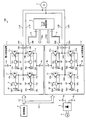
- FIG. 1 is a diagram showing a power conversion system according to a first embodiment of the present invention.
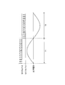
- the figure which shows the waveform of the gate signal generated by the control apparatus which the power conversion system shown in FIG. 1 has, and the waveform of the output voltage by a power conversion apparatus.
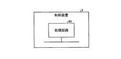
- FIG. 2 is a diagram illustrating a hardware configuration when the functions of the control device illustrated in FIG. 1 are realized by dedicated hardware.
- FIG. 2 is a diagram illustrating a hardware configuration when the functions of the control device illustrated in FIG. 1 are realized by a processor that executes a program stored in a memory.
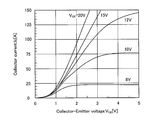
- the figure which shows the example of the relationship between the collector current and the collector-emitter voltage in the switching element which the power conversion system shown in FIG. 1 has.
- FIG. 1 is a diagram showing a power conversion system according to a first embodiment of the present invention. The figure which shows the waveform of the gate signal generated by the control apparatus which the power conversion system shown in FIG. 1 has, and the waveform of the output voltage by a power conversion apparatus
- FIG. 4 is a diagram illustrating a gate voltage adjustment circuit according to a second embodiment of the present invention.
- FIG. 4 is a diagram showing a power conversion system according to a third embodiment of the present invention. The figure which shows the example of a structure of the gate voltage adjustment circuit which the power conversion system shown in FIG. 7 has.
- FIG. 7 is a diagram showing a power conversion system according to a fourth embodiment of the present invention.
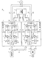
- FIG. 1 is a diagram illustrating a power conversion system 100 according to the first embodiment of the present invention.
- the power conversion system 100 includes power conversion devices 1 and 2 that are a plurality of power conversion devices, a gate voltage adjustment circuit 3 that adjusts a gate voltage, a control device 4 that controls the power conversion devices 1 and 2, a rectifier 5 And
- the power conversion system 100 converts the AC current from the commercial power supply 6 into a DC current once by the rectifying element 5, and further converts the DC current into the AC current by the power converters 1 and 2.
- the power conversion system 100 supplies the converted AC current to the motor 7 as a load device.
- the power converters 1 and 2 are connected in parallel with each other so as to be able to supply an alternating current to the motor 7 which is the same load.
- the number of power conversion devices provided in power conversion system 100 is not limited to two.
- the power conversion system 100 may include three or more power conversion devices connected to each other in parallel.
- the control device 4 generates gate signals G1 and G2, which are common gate signals for controlling the output voltages of the power conversion devices 1 and 2 so that the output voltage of the power conversion system 100 becomes a target value.
- the control device 4 sends the generated gate signal G1 to the power conversion device 1 and sends the generated gate signal G2 to the power conversion device 2.
- the gate signals G1 and G2 are pulse width modulation (PWM) signals.
- PWM pulse width modulation
- the rectifier 5 is a semiconductor rectifier such as a diode bridge. Positive terminal 8c of rectifying element 5 is connected to P terminal 8a of power converter 1 and P terminal 8b of power converter 2. Negative terminal 9c of rectifier 5 is connected to N terminal 9a of power converter 1 and N terminal 9b of power converter 2.
- the rectifying element 5 converts an alternating current from the commercial power supply 6 into a direct current, and supplies the direct current to the power converter 1 and the power converter 2.
- the power converter 1 includes a gate voltage circuit 10a, 10b, 10c, 10d for generating a gate voltage, switching elements 11a, 11b, 11c, 11d, and a gate drive circuit 12a for driving the switching elements 11a, 11b, 11c, 11d. , 12b, 12c, and 12d.
- the gate drive circuits 12a, 12b, 12c, and 12d apply the gate voltages generated by the gate voltage circuits 10a, 10b, 10c, and 10d to the switching elements 11a, 11b, 11c, and 11d to switch the switching elements 11a, 11b, and 11c. , 11d.
- the switching elements 11a, 11b, 11c, 11d are turned on when a gate voltage is applied.
- the gate voltage circuit 10 is referred to without distinguishing each of the gate voltage circuits 10a, 10b, 10c, and 10d.
- the switching element 11 is referred to as each of the switching elements 11a, 11b, 11c, and 11d without distinction.
- the gate drive circuit 12 is referred to as each of the gate drive circuits 12a, 12b, 12c, and 12d without distinction.
- the switching element 11 is an IGBT (Insulated Gate Bipolar Transistor) which is a semiconductor element.
- the switching element 11 may be a MOSFET (Metal-Oxide-Semiconductor Field-Effect Transistor) or a transistor.
- the gate voltage circuit 10a outputs the generated gate voltage to the gate drive circuit 12a.
- Gate voltage circuit 10b outputs the generated gate voltage to gate drive circuit 12b.
- the gate voltage circuit 10c outputs the generated gate voltage to the gate drive circuit 12c.
- the gate voltage circuit 10d outputs the generated gate voltage to the gate drive circuit 12d.
- Each of the gate voltage circuits 10a, 10b, 10c, and 10d can change the level of the gate voltage according to the feedback signal FB1 from the gate voltage adjustment circuit 3.
- the gate drive circuit 12 outputs the gate voltage during a period in which the pulse of the gate signal G1 is on, and stops outputting the gate voltage during a period in which the pulse of the gate signal G1 is off.
- the gate drive circuit 12 switches between output of the gate voltage and output stop according to the gate signal G1.
- the gate drive circuit 12a outputs a gate voltage to a gate electrode of the switching element 11a.
- the gate drive circuit 12b outputs a gate voltage to the gate electrode of the switching element 11b.
- the gate drive circuit 12c outputs a gate voltage to the gate electrode of the switching element 11c.
- the gate drive circuit 12d outputs a gate voltage to the gate electrode of the switching element 11d.
- the gate drive circuit 12 functions as a switch for switching between a closed state for outputting the gate voltage and an open state for stopping the output of the gate voltage.
- the collector terminal of the switching element 11a and the collector terminal of the switching element 11c are connected to the P terminal 8a.
- the emitter terminal of the switching element 11b and the emitter terminal of the switching element 11d are connected to the N terminal 9a.
- Switching element 11a and switching element 11b are connected in series between P terminal 8a and N terminal 9a.
- the switching element 11c and the switching element 11d are connected in series between the P terminal 8a and the N terminal 9a.
- connection point 14A between the emitter terminal of the switching element 11a and the collector terminal of the switching element 11b is connected to the motor 7 via the output line 15A.
- the current sensor 13A detects a current flowing through the output line 15A.
- a connection point 14B between the emitter terminal of the switching element 11c and the collector terminal of the switching element 11d is connected to the motor 7 via an output line 15B.
- the current sensor 13B detects a current flowing through the output line 15B.
- the power converter 1 applies to the motor 7 an output voltage that is the difference between the voltage L1A at the connection point 14A and the voltage L1B at the connection point 14B.
- the switching elements 11a and 11c connected to the P terminal 8a are P-side switching elements on the plus side of the switching elements 11 provided in the power converter 1.
- the switching elements 11b and 11d connected to the N terminal 9a are N-side switching elements on the negative side of the switching elements 11 provided in the power converter 1.
- the configuration of the power conversion device 1 is divided into a P-side component and an N-side component.
- the gate voltage circuits 10a and 10c, the switching elements 11a and 11c, and the gate drive circuits 12a and 12c are P-side components.
- the gate voltage circuits 10b and 10d, the switching elements 11b and 11d, and the gate drive circuits 12b and 12d are N-side components.
- the P side is a portion of the circuit between the P terminal 8a and the N terminal 9a closer to the P terminal 8a than the connection points 14A and 14B.
- the N side is a portion of the circuit between the P terminal 8a and the N terminal 9a closer to the N terminal 9a than the connection points 14A and 14B.
- the configuration of the power conversion device 1 includes a component on the first phase side of the circuit between the P terminal 8a and the N terminal 9a to which the voltage L1A is applied, a P terminal 8a and an N terminal 9a.
- the gate voltage circuits 10a and 10b, the switching elements 11a and 11b, and the gate drive circuits 12a and 12b are components on the first phase side.
- the gate voltage circuits 10c and 10d, the switching elements 11c and 11d, and the gate drive circuits 12c and 12d are components on the second phase side.
- the power converter 2 has the same configuration as the power converter 1.
- the power conversion device 2 includes a gate voltage circuit 20a, 20b, 20c, 20d for generating a gate voltage, switching elements 21a, 21b, 21c, 21d, and a gate drive circuit 22a for driving the switching elements 21a, 21b, 21c, 21d. , 22b, 22c, 22d.
- the gate drive circuits 22a, 22b, 22c, and 22d apply the gate voltages generated by the gate voltage circuits 20a, 20b, 20c, and 20d to the switching elements 21a, 21b, 21c, and 21d to switch the switching elements 21a, 21b, and 21c. , 21d.
- the switching elements 21a, 21b, 21c, 21d are turned on when a gate voltage is applied.
- the gate voltage circuit 20 is referred to as each of the gate voltage circuits 20a, 20b, 20c, and 20d without distinction.
- the switching element 21 is referred to as each of the switching elements 21a, 21b, 21c, 21d without distinction.
- the gate drive circuit 22 is referred to as each of the gate drive circuits 22a, 22b, 22c, and 22d without distinction.
- the switching element 21 is an IGBT that is a semiconductor element.
- the switching element 21 may be a MOSFET or a transistor.
- the gate voltage circuit 20a outputs the generated gate voltage to the gate drive circuit 22a.
- Gate voltage circuit 20b outputs the generated gate voltage to gate drive circuit 22b.
- Gate voltage circuit 20c outputs the generated gate voltage to gate drive circuit 22c.
- the gate voltage circuit 20d outputs the generated gate voltage to the gate drive circuit 22d.
- Each of the gate voltage circuits 20a, 20b, 20c, and 20d can change the level of the gate voltage according to the feedback signal FB2 from the gate voltage adjustment circuit 3.
- the gate drive circuit 22 outputs a gate voltage while the pulse of the gate signal G2 is on, and stops outputting the gate voltage while the pulse of the gate signal G2 is off.
- the gate drive circuit 22 switches between outputting the gate voltage and stopping the output according to the gate signal G2.
- the gate drive circuit 22a outputs a gate voltage to a gate electrode of the switching element 21a.
- the gate drive circuit 22b outputs a gate voltage to the gate electrode of the switching element 21b.
- the gate drive circuit 22c outputs a gate voltage to the gate electrode of the switching element 21c.
- the gate drive circuit 22d outputs a gate voltage to the gate electrode of the switching element 21d.
- the gate drive circuit 22 functions as a switch for switching between a closed state for outputting the gate voltage and an open state for stopping the output of the gate voltage.
- the switching element 21 is in an on state in which a current flows between the collector and the emitter by the application of the gate voltage, and is in an off state in which no current flows between the collector and the emitter by stopping the application of the gate voltage.
- the collector terminal of the switching element 21a and the collector terminal of the switching element 21c are connected to the P terminal 8b.
- the emitter terminal of the switching element 21b and the emitter terminal of the switching element 21d are connected to the N terminal 9b.
- the switching element 21a and the switching element 21b are connected in series between the P terminal 8b and the N terminal 9b.
- the switching element 21c and the switching element 21d are connected in series between the P terminal 8b and the N terminal 9b.
- connection point 24A between the emitter terminal of the switching element 21a and the collector terminal of the switching element 21b is connected to the motor 7 via an output line 25A.
- the current sensor 23A detects a current flowing through the output line 25A.
- a connection point 24B between the emitter terminal of the switching element 21c and the collector terminal of the switching element 21d is connected to the motor 7 via an output line 25B.
- the current sensor 23B detects a current flowing through the output line 25B.
- the power converter 2 applies an output voltage, which is a difference between the voltage L2A at the connection point 24A and the voltage L2B at the connection point 24B, to the motor 7.
- the switching elements 21a and 21c connected to the P terminal 8b are P-side switching elements on the plus side of the switching elements 21 provided in the power converter 2.
- the switching elements 21b and 21d connected to the N terminal 9b are N-side switching elements on the minus side of the switching elements 21 provided in the power converter 2.
- the configuration of the power conversion device 2 is divided into a P-side component and an N-side component.
- the gate voltage circuits 20a and 20c, the switching elements 21a and 21c, and the gate drive circuits 22a and 22c are P-side components.
- the gate voltage circuits 20b and 20d, the switching elements 21b and 21d, and the gate drive circuits 22b and 22d are N-side components.
- the P side is a portion of the circuit between the P terminal 8b and the N terminal 9b closer to the P terminal 8b than the connection points 24A and 24B.
- the N side is a portion of the circuit between the P terminal 8b and the N terminal 9b closer to the N terminal 9b than the connection points 24A and 24B.
- the configuration of the power conversion device 2 includes a first phase side component that is a side to which the voltage L2A is applied, of the circuit between the P terminal 8b and the N terminal 9b, a P terminal 8b and an N terminal 9b. Are divided into components on the second phase side where the voltage L2B is applied.
- the gate voltage circuits 20a and 20b, the switching elements 21a and 21b, and the gate drive circuits 22a and 22b are components on the first phase side.
- the gate voltage circuits 20c and 20d, the switching elements 21c and 21d, and the gate drive circuits 22c and 22d are components on the second phase side.
- the gate voltage adjustment circuit 3 generates feedback signals FB1 and FB2 that change the level of the gate voltage applied to at least one of the switching elements 11 and 21 of the power conversion devices 1 and 2, thereby generating the power conversion devices. Adjustment is performed so that the output voltages of the power conversion devices 1 and 2 become the target values of the output power of each of the power conversion devices 1 and 2.
- the gate voltage adjustment circuit 3 adjusts the average voltage output from each of the power conversion devices 1 and 2 by adjusting the output voltage of each of the power conversion devices 1 and 2 to a target value.
- the average power is power per unit time, for example, per second, and is obtained by multiplying the effective value of the power voltage by the effective value of the current.
- the average power output from each of the power conversion devices 1 and 2 is equal when the average power output from each of the power conversion devices 1 and 2 is the same, that is, of the power supplied to the motor 7 It is not limited to the case where each power converter 1 and 2 bears 50% of the power.
- the current sensor 13A measures the current flowing through the output line 15A, and outputs an electric signal indicating the measurement result to the control device 4.
- the current sensor 13B measures the current flowing through the output line 15B and outputs an electric signal indicating the measurement result to the control device 4.
- the output of the electric signal from the current sensors 13A and 13B to the control device 4 is not shown.
- the control device 4 generates a gate signal G1 whose pulse width is adjusted so that the output voltage of the power conversion device 1 becomes a target value, based on the measurement results of the current sensors 13A and 13B.
- the control device 4 sends the generated gate signal G1 to the gate drive circuit 12.
- control device 4 sends a gate signal G2, which is the same gate signal as the gate signal G1, to the gate drive circuit 22.
- the control device 4 may be provided with a connector that allows the output of the gate signal G2 to the power conversion device 2 by branching the gate signal G1 output to the power conversion device 1.
- the switching elements 11b and 11c perform switching, and the switching elements 11a and 11d stop switching.
- the switching element 11c when the switching element 11c is in the ON state, the current supplied from the rectifying element 5 flows between the collector and the emitter of the switching element 11c.
- the voltage of the P terminal 8a is applied to the output line 15B, and a current flows through the motor 7.
- the switching element 11b When the switching element 11b is on, the current flowing from the motor 7 flows between the collector and the emitter of the switching element 11b.
- the voltage of the N terminal 9a is applied to the output line 15A, and a current flows through the motor 7.
- An output voltage which is a difference between the voltage L1A of the output line 15A and the voltage L2A of the output line 15B is applied to the motor 7.
- the power conversion device 1 applies the output voltage to the motor 7 when the switching elements 11b and 11c are turned on. Also in the period T2, a current flows through the motor 7 by applying an output voltage to both ends of the motor 7.
- the control device 4 controls the power conversion device 2 in the same manner as the power conversion device 1.
- the switching element 21a When the switching element 21a is on, the voltage of the P terminal 8b is applied to the output line 25A.
- the switching element 21d When the switching element 21d is in the ON state, the voltage of the N terminal 9b is applied to the output line 25B.
- the switching element 21c When the switching element 21c is in the ON state, the voltage of the P terminal 8b is applied to the output line 25B.
- the switching element 21b is on, the voltage of the N terminal 9b is applied to the output line 25A.
- the control device 4 alternately repeats a period in which the switching elements 21a and 21d are switched and a period in which the switching elements 21b and 21c are switched.
- the function of the control device 4 is realized by a processing circuit.
- the processing circuit is dedicated hardware mounted on the control device 4.
- the processing circuit may be a processor that executes a program stored in a memory.
- FIG. 3 is a diagram showing a hardware configuration when the functions of the control device 4 shown in FIG. 1 are realized by dedicated hardware.
- the processing circuit 40 which is dedicated hardware includes a single circuit, a composite circuit, a programmed processor, a parallel programmed processor, an ASIC (Application Specific Integrated Circuit), an FPGA (Field-Programmable Gate Array), or an FPGA (Field-Programmable Gate Array). Combination.
- FIG. 4 is a diagram showing a hardware configuration in a case where the functions of the control device 4 shown in FIG. 1 are realized by the processor 41 that executes a program stored in the memory 42.
- the processor 41 and the memory 42 are communicably connected to each other.
- the processor 41 is a CPU (Central Processing Unit), a processing device, an arithmetic device, a microprocessor, a microcomputer, or a DSP (Digital Signal Processor).
- the function of the control device 4 is realized by the processor 41, software, firmware, or a combination of software and firmware. Software or firmware is described as a program and stored in the memory 42.
- the memory 42 is nonvolatile or volatile such as RAM (Random Access Memory), ROM (Read Only Memory), flash memory, EPROM (Erasable Programmable Read Only Memory), and EEPROM (registered trademark) (Electrically Erasable Programmable Read-Only Memory). It is a built-in memory such as a semiconductor memory.
- a part of the function of the control device 4 may be realized by dedicated hardware, and the other part of the function of the control device 4 may be realized by software or firmware. As described above, the function of the control device 4 can be realized by hardware, software, firmware, or a combination thereof.
- any one of the power conversion devices 1 and 2 has a high load. Assuming that the power converter 1 has a higher load than the power converter 2, if the power output by the power converter 1 reaches the limit power that can be supplied, the power exceeding the power is used. The power converter 1 cannot supply. When such a power limitation occurs in the power conversion device 1, the power conversion device 2 is controlled by the same gate signal as the power conversion device 1, so that when the power limitation in the power conversion device 1 occurs. It becomes impossible to supply power higher than the supplied power.
- a difference may occur between the output voltage of the power conversion device 1 and the output voltage of the power conversion device 2, so that a lateral current may occur between the power conversion device 1 and the power conversion device 2.
- the lateral current flows from the power converter 1 to the power converter 2.
- the power conversion system 100 If there is no difference in voltage, power of 20 kW can be supplied to the motor 7.
- 4 kW of the 20 kW power that could be supplied to the motor 7 is consumed between the power converters 1 and 2, and the power supplied to the motor 7 is It drops to 16 kW.
- the efficiency of power conversion is reduced due to the generation of the lateral current.
- the difference between the output voltage of the power converter 1 and the output voltage of the power converter 2 can be caused by the difference between the collector-emitter saturation voltages of the switching elements 11 and 21.
- the collector-emitter saturation voltage is a voltage between the collector and the emitter when the switching elements 11 and 21 are saturated.
- the difference between the output voltage of the power converter 1 and the output voltage of the power converter 2 is the difference between the collector-emitter saturation voltage, the difference between the voltage drops of the gate drive circuits 12 and 22, and the pulse of the gate signals G1 and G2. It may be caused by factors such as a width error or a gate voltage error.
- the power conversion system 100 changes the level of the gate voltage applied to at least one of the power conversion devices 1 and 2 by the gate voltage adjustment circuit 3 shown in FIG. An adjustment is performed to make the output voltages of the devices 1 and 2 coincide with each other.
- the load of power supply can be leveled such that the load of power supply by each of the power conversion devices 1 and 2 falls within a range of about 40% to 60%.
- the power conversion system 100 drives the load devices by controlling the plurality of power conversion devices 1 and 2 so that the average power output from each of the plurality of power conversion devices 1 and 2 becomes equal. can do.
- the current sensors 13A, 13B, 23A, and 23B measure the instantaneous value of the current. However, in the first embodiment, it is assumed that the current sensors 13A, 13B, 23A, and 23B output the effective value of the current for convenience. .
- the current sensors 13A, 13B, 23A, and 23B output an effective value as a measurement result
- the current sensors 13A, 13B, 23A, and 23B include a circuit for converting an instantaneous value to an effective value, or a circuit for converting the instantaneous value. Arithmetic means for calculating the effective value is provided. Such a circuit and an arithmetic unit may be provided in the gate voltage adjustment circuit 3 or the control device 4.
- the power conversion system 100 aims at controlling the average power output by each of the plurality of power conversion devices 1 and 2 to be equal. Therefore, controlling to match the instantaneous value of the current and controlling to match the effective value of the current have the same meaning as a result.
- the current sensor 13A measures the effective value of the output current flowing through the output line 15A.
- the current sensor 13B measures the effective value of the output current flowing through the output line 15B. Thereby, current sensors 13A and 13B measure the effective value of output current I1 output from power conversion device 1, and output an electric signal indicating the measurement result to gate voltage adjustment circuit 3.
- the current sensor 23A measures the effective value of the output current flowing through the output line 25A.
- the current sensor 23B measures the effective value of the output current flowing through the output line 25B.
- current sensors 23A and 23B measure the effective value of output current I2 output from power conversion device 2, and output an electric signal indicating the measurement result to gate voltage adjustment circuit 3.
- the gate voltage adjustment circuit 3 obtains a difference between the effective value of the output current I1 and the effective value of the output current I2.
- the gate voltage adjustment circuit 3 generates a feedback signal FB1 of the power conversion device 1 and a feedback signal FB2 of the power conversion device 2 based on the obtained difference.
- Gate voltage adjustment circuit 3 outputs feedback signal FB1 to power converter 1 and outputs feedback signal FB2 to power converter 2.
- the gate voltage adjustment circuit 3 generates feedback signals FB1 and FB2 for changing the levels of the gate signals G1 and G2 based on the result of comparing the output currents I1 and I2 from the plurality of power converters 1 and 2. The adjustment is performed so that the output voltages of the plurality of power conversion devices 1 and 2 are matched.
- the gate voltage adjustment circuit 3 performs adjustment for equalizing the average voltage output from each of the plurality of power conversion devices 1 and 2.
- the adjustment for making the output voltages of the plurality of power conversion devices 1 and 2 coincide with each other includes not only the adjustment for making the voltage values of the output voltages of the power conversion devices 1 and 2 the same, but also the adjustment of the power conversion device 1. , 2 are adjusted so that the voltage values of the output voltages are close to each other.
- the gate voltage adjustment circuit 3 When the effective value of the output current I1 is higher than the effective value of the output current I2, the output voltage of the power conversion device 1 is higher than the output voltage of the power conversion device 2. In this case, the gate voltage adjustment circuit 3 generates a feedback signal FB1 for lowering the level of the gate voltage of the gate voltage circuit 10. Gate voltage adjustment circuit 3 outputs generated feedback signal FB1 to each gate voltage circuit 10 of power conversion device 1. Gate voltage circuit 10 lowers the level of the gate voltage by the level corresponding to feedback signal FB1. According to the relationship shown in FIG. 5, in the switching element 11, the collector current decreases as the level of the gate voltage decreases. As the collector current decreases, the output voltage of the switching element 11 decreases. As a result, the gate voltage adjustment circuit 3 performs adjustment for lowering the level of the output voltage of the power conversion device 1.
- the gate voltage adjustment circuit 3 when the effective value of the output current I1 is higher than the effective value of the output current I2, the gate voltage adjustment circuit 3 generates the feedback signal FB2 for increasing the level of the gate voltage of the gate voltage circuit 20. Thereby, the gate voltage adjustment circuit 3 performs adjustment for increasing the level of the output voltage of the power conversion device 2.
- the gate voltage adjustment circuit 3 When the effective value of the output current I1 is lower than the effective value of the output current I2, the gate voltage adjustment circuit 3 outputs the feedback signal FB1 for increasing the level of the gate voltage of the gate voltage circuit 10 or the gate voltage circuit 20. To generate a feedback signal FB2 for lowering the level of the gate voltage. As described above, the gate voltage adjustment circuit 3 changes the gate voltage of the power conversion device 1 or the gate voltage of the power conversion device 2 to reduce the difference between the output voltages of the power conversion devices 1 and 2. The gate voltage adjustment circuit 3 repeats a change in the gate voltage according to the result of comparing the effective value of the output current I1 and the effective value of the output current I2, thereby providing a difference between the levels of the output voltages of the power conversion devices 1 and 2. Is converged.
- Each of the gate voltage circuits 10a, 10b, 10c, and 10d adjusts a gate voltage based on the feedback signal FB1.
- Each of gate voltage circuits 20a, 20b, 20c, and 20d adjusts a gate voltage based on feedback signal FB2.
- the gate voltage adjustment circuit 3 performs the adjustment to make the output voltages of the power conversion devices 1 and 2 coincide with each other, thereby making the adjustment to make the average voltages output from each of the power conversion devices 1 and 2 uniform. Do.
- the gate voltage adjustment circuit 3 performs the gate operation when the effective value of the output current I1 is higher than the effective value of the output current I2 or when the effective value of the output current I1 is lower than the effective value of the output current I2.
- Both the feedback signal FB1 for changing the level of the gate voltage of the voltage circuit 10 and the feedback signal FB2 for changing the level of the gate voltage of the gate voltage circuit 20 may be generated.
- the gate voltage adjustment circuit 3 reduces the difference between the output voltages of the power converters 1 and 2 by changing the output voltage of the power converter 1 and the output voltage of the power converter 2. Thereby, the gate voltage adjustment circuit 3 can perform adjustment for making the output voltages of the power conversion devices 1 and 2 coincide with each other.
- the power conversion system 100 can reduce the generation of the lateral current by performing adjustment for matching the output voltages of the power conversion devices 1 and 2 with each other.
- the power conversion system 100 can perform power conversion with high efficiency by reducing the generation of the lateral current. Since the power conversion system 100 can equalize the load of power supply by each of the power conversion devices 1 and 2, it is possible to reduce a situation in which one of the power conversion devices 1 and 2 is overloaded. Thus, power conversion system 100 can suppress concentration of aging on one of power conversion devices 1 and 2.
- the power conversion system 100 includes the gate voltage adjustment circuit 3 and operates according to the gate signal from the control device 4 except that the level of the gate voltage in the gate voltage circuits 10 and 20 can be changed by the feedback signals FB1 and FB2.
- the same configuration as in the case where the existing power conversion device that operates alone is provided can be used.
- the software configuration of the control device 4 does not need to add or change the configuration for adjusting the output voltage of each of the power converters 1 and 2.
- the control device 4 can have the same configuration as that for controlling an existing power conversion device, except that the control device 4 can output the gate signals G1 and G2 to the plurality of power conversion devices 1 and 2.
- the power converters 1 and 2 can have the same configuration as an existing power converter, except that the level of the gate voltage can be changed.
- the power conversion system 100 can reduce the addition to the existing configuration and the change from the existing configuration. Since the power conversion system 100 can reduce additions to existing configurations and changes from existing configurations, the power conversion system 100 can have a simple configuration and reduce manufacturing costs.
- power conversion system 100 includes gate voltage adjustment circuit 3 that adjusts the output voltage of each of power conversion devices 1 and 2 to match by changing the level of the gate voltage.
- the difference between the output voltages of the power conversion devices 1 and 2 can be reduced with a simple configuration.
- the power conversion system 100 reduces the difference between the output voltages of the power conversion devices 1 and 2 so that the output currents flowing from the power conversion devices 1 and 2 to the load device are close to each other. Since the adjustment is performed, the average power output from each of the power conversion devices 1 and 2 can be equalized. Thereby, the power conversion system 100 can control the plurality of power conversion devices 1 and 2 with a simple configuration so that the average power output from each of the power conversion devices 1 and 2 is equalized. Play.
- the gate voltage adjustment circuit 3 adjusts the output voltage of each of the plurality of power conversion devices 1 and 2 by changing the level of the gate voltage applied to at least one of the plurality of power conversion devices 1 and 2. Any configuration is possible, and any configuration can be adopted. In the second embodiment, a configuration example of the gate voltage adjustment circuit 3 will be described.
- FIG. FIG. 6 is a diagram illustrating the gate voltage adjustment circuit 3 according to the second embodiment of the present invention.
- the electric signal indicating the effective value of the output current I1 from the power conversion device 1 and the electric signal indicating the effective value of the output current I2 from the power conversion device 2 are input to the gate voltage adjustment circuit 3.
- the gate voltage adjustment circuit 3 has comparators 31 and 32.
- the electric signal indicating the effective value of the output current I1 is input to the inverting input terminal of the comparator 31 and the non-inverting input terminal of the comparator 32.
- An electric signal indicating the effective value of the output current I2 is input to the non-inverting input terminal of the comparator 31 and the inverting input terminal of the comparator 32.
- the comparator 31 generates a feedback signal FB1 based on the difference between the effective value of the output current I1 and the effective value of the output current I2.
- the comparator 32 generates a feedback signal FB2 based on the difference between the effective value of the output current I1 and the effective value of the output current I2.
- the gate voltage adjustment circuit 3 outputs the feedback signal FB1 to the power conversion device 1 and outputs the feedback signal FB2 to the power conversion device 2. Thereby, the gate voltage adjustment circuit 3 can adjust the output voltages of the plurality of power conversion devices 1 and 2 to match each other based on the result of comparing the effective values of the output currents I1 and I2.
- the power conversion system 100 adjusts the output voltage of each of the power conversion devices 1 and 2 so that the output current flowing from each of the power conversion devices 1 and 2 to the load device also has the value of the output current. Are adjusted to be close to each other, so that the average power output from each of the power conversion devices 1 and 2 can be made uniform. Thereby, the power conversion system 100 can control the plurality of power conversion devices 1 and 2 with a simple configuration so that the average power output from each of the power conversion devices 1 and 2 is equalized. Play.
- FIG. 7 is a diagram illustrating a power conversion system 101 according to the third embodiment of the present invention.
- the gate voltage adjustment circuit 33 of the power conversion system 101 matches the output voltages of each of the plurality of power conversion devices 1 and 2 based on the result of comparing the output voltages V1 and V2 from the plurality of power conversion devices 1 and 2.
- Make adjustments to make In the third embodiment, the same components as those in the first and second embodiments are denoted by the same reference numerals, and a configuration different from the first and second embodiments will be mainly described.
- the power conversion device 1 has the current detection resistors 16A and 16B.
- the current detection resistor 16A is connected to the output line 15A.
- the current detection resistor 16B is connected to the output line 15B.
- the power conversion device 2 has current detection resistors 26A and 26B.
- the current detection resistor 26A is connected to the output line 25A.
- the current detection resistor 26B is connected to the output line 25B.
- the control device 4 measures the current flowing through the output lines 15A and 15B based on the voltage drop generated in the current detection resistors 16A and 16B and the resistance values of the current detection resistors 16A and 16B.
- the control device 4 generates a gate signal G1 whose pulse width is adjusted so that the output voltage of the power conversion device 1 becomes a target value, based on the measurement result of the current.
- the control device 4 sends the generated gate signal G1 to the gate drive circuit 12. Further, the control device 4 sends a gate signal G2, which is the same gate signal as the gate signal G1, to the gate drive circuit 22.
- Gate voltage adjustment circuit 33 detects output voltage V1 of power conversion device 1 based on a voltage drop generated in current detection resistors 16A and 16B. Both ends of the current detection resistors 26A and 26B are connected to a gate voltage adjustment circuit 33. Gate voltage adjustment circuit 33 detects output voltage V2 of power conversion device 2 based on the voltage drop generated in current detection resistors 26A and 26B.
- the gate voltage adjustment circuit 33 adjusts the output voltage of each of the plurality of power conversion devices 1 and 2 by changing the level of the gate voltage applied to at least one of the plurality of power conversion devices 1 and 2. I do.
- the gate voltage adjustment circuit 33 may have any configuration as long as such adjustment is possible.
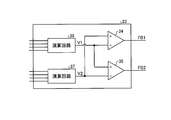
- FIG. 8 is a diagram showing a configuration example of the gate voltage adjustment circuit 33 included in the power conversion system 101 shown in FIG.
- the gate voltage adjustment circuit 33 has comparators 34 and 35 and operation circuits 36 and 37.
- the operation circuit 36 detects a voltage drop generated at both ends of the current detection resistor 16A and a voltage drop generated at both ends of the current detection resistor 16B.
- the arithmetic circuit 36 detects the output voltage V1 of the power conversion device 1 based on the voltage drop generated in the current detection resistors 16A and 16B, and obtains the effective value of the output voltage V1.
- the arithmetic circuit 36 outputs an electric signal indicating the effective value of the output voltage V1.
- the arithmetic circuit 37 detects a voltage drop generated at both ends of the current detection resistor 26A and a voltage drop generated at both ends of the current detection resistor 26B.
- the arithmetic circuit 37 detects the output voltage V2 of the power conversion device 2 based on the voltage drop generated in the current detection resistors 26A and 26B, and obtains the effective value of the output voltage V2.
- the arithmetic circuit 37 outputs an electric signal indicating the effective value of the output voltage V2.
- the electric signal indicating the effective value of the output voltage V1 is input to the inverting input terminal of the comparator 34 and the non-inverting input terminal of the comparator 35.
- An electric signal indicating the effective value of the output voltage V2 is input to the non-inverting input terminal of the comparator 34 and the inverting input terminal of the comparator 35.
- the comparator 34 generates a feedback signal FB1 based on the difference between the effective value of the output voltage V1 and the effective value of the output voltage V2.
- the comparator 35 generates a feedback signal FB2 based on the difference between the effective value of the output voltage V1 and the effective value of the output voltage V2.
- the gate voltage adjustment circuit 33 outputs the feedback signal FB1 to the power converter 1 and outputs the feedback signal FB2 to the power converter 2. Thereby, the gate voltage adjustment circuit 33 can perform adjustment for matching the output voltages of the plurality of power conversion devices 1 and 2 based on the result of comparing the effective values of the output voltages V1 and V2.
- the power conversion system 101 includes the gate voltage adjustment circuit 33 that adjusts the output voltage of each of the plurality of power conversion devices 1 and 2 by changing the level of the gate voltage.
- the difference between the output voltages of the power conversion devices 1 and 2 can be reduced with a simple configuration.
- the power conversion system 101 reduces the difference between the output voltages of the power conversion devices 1 and 2 so that the output currents flowing from the power conversion devices 1 and 2 to the load device are close to each other. Since the adjustment is performed, the average power output from each of the power conversion devices 1 and 2 can be equalized. Thereby, the power conversion system 101 can control the plurality of power conversion devices 1 and 2 with a simple configuration so that the average power output from each of the power conversion devices 1 and 2 is equalized. Play.
- FIG. 9 is a diagram illustrating the power conversion system 102 according to the fourth embodiment of the present invention.
- Power conversion system 102 has gate voltage circuits 17 and 27.
- the same components as those in the above-described first to third embodiments are denoted by the same reference numerals, and a configuration different from the first to third embodiments will be mainly described.
- the power conversion system 100 adjusts the gate voltage by inputting the feedback signal FB1 to each of the gate voltage circuits 10a, 10b, 10c, and 10d, and adjusts the gate voltage circuits 20a, 20b, 20c, and 20d.
- adjustment is performed to make the output voltages of the plurality of power converters 1 and 2 coincide with each other.
- power converter 1 includes a gate voltage circuit 17 instead of gate voltage circuits 10a, 10b, 10c, and 10d.
- power conversion device 2 includes a gate voltage circuit 27 instead of gate voltage circuits 20a, 20b, 20c, and 20d.
- the gate voltage circuits 17 and 27 are switching power supplies with multiple outputs. Gate voltage circuit 17 outputs a gate voltage generated according to feedback signal FB1 to gate drive circuits 12a, 12b, 12c, and 12d. Gate voltage circuit 27 outputs a gate voltage generated according to feedback signal FB2 to gate drive circuits 22a, 22b, 22c, 22d.
- the gate voltage circuits 17 and 27 use one of the multiple outputs as a control target and change the level of the gate voltage for the control target.
- the gate voltage circuits 17 and 27 change the gate voltage of the outputs other than the control target among the multiple outputs in conjunction with the change of the gate voltage of the control target.
- the gate voltage circuits 17 and 27 are controlled by setting the configuration for each output other than the control target to be the same as the configuration for the output to be controlled, for example, by setting the number of turns of the transformer to be the same.
- the gate voltage is linked to the gate voltage for the target.
- the power conversion system 102 may include the same gate voltage adjustment circuit 3 as the second embodiment or the same gate voltage adjustment circuit 33 as the third embodiment.
- power conversion system 102 adjusts the output voltages of power conversion devices 1 and 2 to coincide with each other by changing gate voltages of gate voltage circuits 17 and 27 according to feedback signals FB1 and FB2. Do.
- the power conversion system 102 adjusts the output voltage from each of the power conversion devices 1 and 2 so that the output currents flowing from the power conversion devices 1 and 2 to the load device are adjusted to be close to each other by adjusting the output voltages of the power conversion devices 1 and 2 to match each other. Therefore, the average power output from each of the power conversion devices 1 and 2 can be equalized.
- the power conversion system 102 can control the plurality of power conversion devices 1 and 2 with a simple configuration so that the average power output from each of the power conversion devices 1 and 2 is equalized. Play.
- 1,2 power conversion device, 3,33 gate voltage adjustment circuit, 4 control device 5 rectifier, 6 commercial power supply, 7 motor, 8a, 8b P terminal, 8c plus terminal, 9a, 9b N terminal, 9c minus terminal, 10, 10a, 10b, 10c, 10d, 17, 20, 20a, 20b, 20c, 20d, 27 ⁇ gate voltage circuit, 11, 11a, 11b, 11c, 11d, 21, 21a, 21b, 21c, 21d ⁇ switching element, 12 , 12a, 12b, 12c, 12d, 22, 22a, 22b, 22c, 22d ⁇ gate drive circuit, 13A, 13B, 23A, 23B ⁇ current sensor, 14A, 14B, 24A, 24B ⁇ connection point, 15A, 15B, 25A, 25B ⁇ output Line, 16A, 16B, 26A, 26B current detection resistor, 31, 32, 34, 3 Comparator, 36 and 37 arithmetic circuits, 40 processing circuit, 41 a processor, 42 a memory, 100, 101, 102 power
Landscapes
- Engineering & Computer Science (AREA)
- Power Engineering (AREA)
- Inverter Devices (AREA)
Abstract
電力変換システム(100)は、ゲート電圧が印加されることによってオン状態となるスイッチング素子(11,21)が各々に設けられており、かつ同一の負荷へ交流電力を供給可能に互いに並列に接続されている複数の電力変換装置(1,2)と、複数のスイッチング素子(11,21)のうち少なくとも1つに印加されるゲート電圧のレベルを変化させるフィードバック信号を生成することによって、複数の電力変換装置(1,2)の各々から出力される平均電力を均等にさせる調整を行うゲート電圧調整回路(3)と、を備える。
Description
本発明は、複数の電力変換装置を備える電力変換システムに関する。
複数の電力変換装置の並列運転によって、単独の電力変換装置を運転する場合よりも電力容量を増大可能とする電力変換システムが知られている。複数の電力変換装置は、同一の負荷へ交流電流を出力可能に互いに並列に接続される。電力変換システムは、交流電流を一旦直流電流へ変換し、さらに各電力変換装置にて直流電流を交流電流へ変換することにより、交流電圧の周波数あるいは交流電圧のレベルを変化させる。
複数の電力変換装置を並列運転させる場合に、電力変換装置ごとの出力電圧に差が生じることにより、複数の電力変換装置のいずれかの負荷が他の電力変換装置の負荷よりも高くなる。また、各電力変換装置の出力電圧の差によって、電力変換装置の間のループ回路を循環する電流である循環電流が生じることがある。循環電流は、横電流とも称される。横電流は負荷である装置の駆動に寄与しないことから、電力変換システムは、横電流の発生により電力変換の効率が低下することになる。
特許文献1には、各電力変換装置におけるゲート信号の同期を可能とする電力変換システムが開示されている。ゲート信号は、各電力変換装置に備えられているスイッチング素子のゲートに入力される。特許文献1によると、各電力変換装置は、制御装置との間の通信によって、電圧指令と、ゲート信号の同期のための同期信号とを受信して、ゲート信号を生成する。電力変換システムは、各電力変換装置におけるゲート信号の同期によって、各電力変換装置により交流電流が出力されるタイミングのずれを抑制可能とし、出力電圧の差を低減する。電力変換システムは、出力電圧の差を低減することによって、各電力変換装置によって供給される平均電力を均等にさせることができる。
上記特許文献1にかかる従来の電力変換システムには、制御装置からのゲート信号にしたがって単独で運転する既存の電力変換装置と同様の構成が備えられるほかに、同期信号の送受信のための通信機能とゲート信号の同期のための処理機能とが追加されている。従来の電力変換システムは、かかる機能の実現のための構成が追加されることで、既存の電力変換装置を備える場合の構成からの大幅な変更を要し、構成が複雑になるという問題があった。
本発明は、上記に鑑みてなされたものであって、簡易な構成によって、各電力変換装置から出力される平均電力が均等になるように複数の電力変換装置を制御可能とする電力変換システムを得ることを目的とする。
上述した課題を解決し、目的を達成するために、本発明にかかる電力変換システムは、ゲート電圧が印加されることによってオン状態となるスイッチング素子が各々に設けられており、かつ同一の負荷へ交流電力を供給可能に互いに並列に接続されている複数の電力変換装置と、複数のスイッチング素子のうち少なくとも1つに印加されるゲート電圧のレベルを変化させるフィードバック信号を生成することによって、複数の電力変換装置の各々から出力される平均電力を均等にさせる調整を行うゲート電圧調整回路と、を備える。
本発明にかかる電力変換システムは、簡易な構成によって、各電力変換装置から出力される平均電力が均等になるように複数の電力変換装置を制御することができるという効果を奏する。
以下に、本発明の実施の形態にかかる電力変換システムを図面に基づいて詳細に説明する。なお、この実施の形態によりこの発明が限定されるものではない。
実施の形態1.
図1は、本発明の実施の形態1にかかる電力変換システム100を示す図である。電力変換システム100は、複数の電力変換装置である電力変換装置1,2と、ゲート電圧を調整するゲート電圧調整回路3と、電力変換装置1,2を制御する制御装置4と、整流素子5とを備える。
図1は、本発明の実施の形態1にかかる電力変換システム100を示す図である。電力変換システム100は、複数の電力変換装置である電力変換装置1,2と、ゲート電圧を調整するゲート電圧調整回路3と、電力変換装置1,2を制御する制御装置4と、整流素子5とを備える。
電力変換システム100は、商用電源6からの交流電流を整流素子5にて一旦直流電流へ変換し、さらに各電力変換装置1,2にて直流電流を交流電流へ変換する。電力変換システム100は、負荷装置であるモータ7へ変換後の交流電流を供給する。電力変換装置1,2は、同一の負荷であるモータ7へ交流電流を供給可能に互いに並列に接続されている。電力変換システム100に備えられる電力変換装置は2つに限られない。電力変換システム100は、互いに並列に接続された3つ以上の電力変換装置を備えていても良い。
制御装置4は、電力変換システム100の出力電圧が目標値となるように電力変換装置1,2の出力電圧を制御するための共通のゲート信号であるゲート信号G1,G2を生成する。制御装置4は、生成されたゲート信号G1を電力変換装置1へ送るとともに、生成されたゲート信号G2を電力変換装置2へ送る。ゲート信号G1,G2は、パルス幅変調(Pulse Width Modulation:PWM)信号である。ゲート信号G1,G2のパルス幅が変化することによって、モータ7へ印加される電流の電流値が変化する。具体的には、パルス幅が小さいほど電流値は小さくなり、パルス幅が大きいほど電流値は大きくなる。
整流素子5は、ダイオードブリッジといった半導体整流素子である。整流素子5のプラス端子8cは、電力変換装置1のP端子8aと電力変換装置2のP端子8bとに接続されている。整流素子5のマイナス端子9cは、電力変換装置1のN端子9aと電力変換装置2のN端子9bとに接続されている。整流素子5は、商用電源6からの交流電流を直流電流へ変換し、電力変換装置1と電力変換装置2とへ直流電流を供給する。
電力変換装置1は、ゲート電圧を生成するゲート電圧回路10a,10b,10c,10dと、スイッチング素子11a,11b,11c,11dと、スイッチング素子11a,11b,11c,11dを駆動するゲート駆動回路12a,12b,12c,12dとを有する。ゲート駆動回路12a,12b,12c,12dは、ゲート電圧回路10a,10b,10c,10dによって生成されたゲート電圧をスイッチング素子11a,11b,11c,11dへ印加することによってスイッチング素子11a,11b,11c,11dを駆動する。スイッチング素子11a,11b,11c,11dは、ゲート電圧が印加されることによってオン状態となる。なお、ゲート電圧回路10とは、ゲート電圧回路10a,10b,10c,10dの各々を区別せずに称したものとする。スイッチング素子11とは、スイッチング素子11a,11b,11c,11dの各々を区別せずに称したものとする。ゲート駆動回路12とは、ゲート駆動回路12a,12b,12c,12dの各々を区別せずに称したものとする。スイッチング素子11は、半導体素子であるIGBT(Insulated Gate Bipolar Transistor)である。スイッチング素子11は、MOSFET(Metal-Oxide-Semiconductor Field-Effect Transistor)またはトランジスタであっても良い。
ゲート電圧回路10aは、生成されたゲート電圧をゲート駆動回路12aへ出力する。ゲート電圧回路10bは、生成されたゲート電圧をゲート駆動回路12bへ出力する。ゲート電圧回路10cは、生成されたゲート電圧をゲート駆動回路12cへ出力する。ゲート電圧回路10dは、生成されたゲート電圧をゲート駆動回路12dへ出力する。各ゲート電圧回路10a,10b,10c,10dは、ゲート電圧調整回路3からのフィードバック信号FB1に従ってゲート電圧のレベルの高低を変化させることができる。
ゲート駆動回路12は、ゲート信号G1のパルスがオンである期間においてゲート電圧を出力し、ゲート信号G1のパルスがオフである期間においてゲート電圧の出力を停止する。ゲート駆動回路12は、ゲート信号G1にしたがって、ゲート電圧の出力と出力停止とを切り換える。ゲート駆動回路12aは、スイッチング素子11aのゲート電極へゲート電圧を出力する。ゲート駆動回路12bは、スイッチング素子11bのゲート電極へゲート電圧を出力する。ゲート駆動回路12cは、スイッチング素子11cのゲート電極へゲート電圧を出力する。ゲート駆動回路12dは、スイッチング素子11dのゲート電極へゲート電圧を出力する。ゲート駆動回路12は、ゲート電圧を出力する閉状態とゲート電圧の出力を停止する開状態とを切り換えるスイッチの機能を果たす。
スイッチング素子11は、ゲート電圧の印加によってコレクタとエミッタとの間に電流が流れるオン状態となり、ゲート電圧の印加が停止されることによってコレクタとエミッタとの間に電流が流れないオフ状態となる。
スイッチング素子11aのコレクタ端子とスイッチング素子11cのコレクタ端子とは、P端子8aに接続されている。スイッチング素子11bのエミッタ端子とスイッチング素子11dのエミッタ端子とは、N端子9aに接続されている。スイッチング素子11aとスイッチング素子11bとは、P端子8aとN端子9aとの間にて直列に接続されている。スイッチング素子11cとスイッチング素子11dとは、P端子8aとN端子9aとの間にて直列に接続されている。
スイッチング素子11aのエミッタ端子とスイッチング素子11bのコレクタ端子との接続点14Aは、出力線15Aを介してモータ7に接続されている。電流センサ13Aは、出力線15Aを流れる電流を検出する。スイッチング素子11cのエミッタ端子とスイッチング素子11dのコレクタ端子との接続点14Bは、出力線15Bを介してモータ7に接続されている。電流センサ13Bは、出力線15Bを流れる電流を検出する。電力変換装置1は、接続点14Aの電圧L1Aと接続点14Bの電圧L1Bとの差である出力電圧をモータ7に印加する。
P端子8aに接続されたスイッチング素子11a,11cは、電力変換装置1に設けられたスイッチング素子11のうちプラス側であるP側のスイッチング素子である。N端子9aに接続されたスイッチング素子11b,11dは、電力変換装置1に設けられたスイッチング素子11のうちマイナス側であるN側のスイッチング素子である。電力変換装置1の構成は、P側の構成要素とN側の構成要素とに分けられる。ゲート電圧回路10a,10cとスイッチング素子11a,11cとゲート駆動回路12a,12cとは、P側の構成要素である。ゲート電圧回路10b,10dとスイッチング素子11b,11dとゲート駆動回路12b,12dとは、N側の構成要素である。P側とは、P端子8aとN端子9aとの間の回路のうち接続点14A,14BよりもP端子8a側の部分とする。N側とは、P端子8aとN端子9aとの間の回路のうち接続点14A,14BよりもN端子9a側の部分とする。
また、電力変換装置1の構成は、P端子8aとN端子9aとの間の回路のうち電圧L1Aが印加される側である第1相側の構成要素と、P端子8aとN端子9aとの間の回路のうち電圧L1Bが印加される側である第2相側の構成要素とに分けられる。ゲート電圧回路10a,10bとスイッチング素子11a,11bとゲート駆動回路12a,12bとは、第1相側の構成要素である。ゲート電圧回路10c,10dとスイッチング素子11c,11dとゲート駆動回路12c,12dとは、第2相側の構成要素である。
電力変換装置2は、電力変換装置1と同様の構成を備える。電力変換装置2は、ゲート電圧を生成するゲート電圧回路20a,20b,20c,20dと、スイッチング素子21a,21b,21c,21dと、スイッチング素子21a,21b,21c,21dを駆動するゲート駆動回路22a,22b,22c,22dとを有する。ゲート駆動回路22a,22b,22c,22dは、ゲート電圧回路20a,20b,20c,20dによって生成されたゲート電圧をスイッチング素子21a,21b,21c,21dへ印加することによってスイッチング素子21a,21b,21c,21dを駆動する。スイッチング素子21a,21b,21c,21dは、ゲート電圧が印加されることによってオン状態となる。なお、ゲート電圧回路20とは、ゲート電圧回路20a,20b,20c,20dの各々を区別せずに称したものとする。スイッチング素子21とは、スイッチング素子21a,21b,21c,21dの各々を区別せずに称したものとする。ゲート駆動回路22とは、ゲート駆動回路22a,22b,22c,22dの各々を区別せずに称したものとする。スイッチング素子21は、半導体素子であるIGBTである。スイッチング素子21は、MOSFETまたはトランジスタであっても良い。
ゲート電圧回路20aは、生成されたゲート電圧をゲート駆動回路22aへ出力する。ゲート電圧回路20bは、生成されたゲート電圧をゲート駆動回路22bへ出力する。ゲート電圧回路20cは、生成されたゲート電圧をゲート駆動回路22cへ出力する。ゲート電圧回路20dは、生成されたゲート電圧をゲート駆動回路22dへ出力する。各ゲート電圧回路20a,20b,20c,20dは、ゲート電圧調整回路3からのフィードバック信号FB2に従ってゲート電圧のレベルの高低を変化させることができる。
ゲート駆動回路22は、ゲート信号G2のパルスがオンである期間においてゲート電圧を出力し、ゲート信号G2のパルスがオフである期間においてゲート電圧の出力を停止する。ゲート駆動回路22は、ゲート信号G2にしたがって、ゲート電圧の出力と出力停止とを切り換える。ゲート駆動回路22aは、スイッチング素子21aのゲート電極へゲート電圧を出力する。ゲート駆動回路22bは、スイッチング素子21bのゲート電極へゲート電圧を出力する。ゲート駆動回路22cは、スイッチング素子21cのゲート電極へゲート電圧を出力する。ゲート駆動回路22dは、スイッチング素子21dのゲート電極へゲート電圧を出力する。ゲート駆動回路22は、ゲート電圧を出力する閉状態とゲート電圧の出力を停止する開状態とを切り換えるスイッチの機能を果たす。
スイッチング素子21は、ゲート電圧の印加によってコレクタとエミッタとの間に電流が流れるオン状態となり、ゲート電圧の印加が停止されることによってコレクタとエミッタとの間に電流が流れないオフ状態となる。
スイッチング素子21aのコレクタ端子とスイッチング素子21cのコレクタ端子とは、P端子8bに接続されている。スイッチング素子21bのエミッタ端子とスイッチング素子21dのエミッタ端子とは、N端子9bに接続されている。スイッチング素子21aとスイッチング素子21bとは、P端子8bとN端子9bとの間にて直列に接続されている。スイッチング素子21cとスイッチング素子21dとは、P端子8bとN端子9bとの間にて直列に接続されている。
スイッチング素子21aのエミッタ端子とスイッチング素子21bのコレクタ端子との接続点24Aは、出力線25Aを介してモータ7に接続されている。電流センサ23Aは、出力線25Aを流れる電流を検出する。スイッチング素子21cのエミッタ端子とスイッチング素子21dのコレクタ端子との接続点24Bは、出力線25Bを介してモータ7に接続されている。電流センサ23Bは、出力線25Bを流れる電流を検出する。電力変換装置2は、接続点24Aの電圧L2Aと接続点24Bの電圧L2Bとの差である出力電圧をモータ7に印加する。
P端子8bに接続されたスイッチング素子21a,21cは、電力変換装置2に設けられたスイッチング素子21のうちプラス側であるP側のスイッチング素子である。N端子9bに接続されたスイッチング素子21b,21dは、電力変換装置2に設けられたスイッチング素子21のうちマイナス側であるN側のスイッチング素子である。電力変換装置2の構成は、P側の構成要素とN側の構成要素とに分けられる。ゲート電圧回路20a,20cとスイッチング素子21a,21cとゲート駆動回路22a,22cとは、P側の構成要素である。ゲート電圧回路20b,20dとスイッチング素子21b,21dとゲート駆動回路22b,22dとは、N側の構成要素である。P側とは、P端子8bとN端子9bとの間の回路のうち接続点24A,24BよりもP端子8b側の部分とする。N側とは、P端子8bとN端子9bとの間の回路のうち接続点24A,24BよりもN端子9b側の部分とする。
また、電力変換装置2の構成は、P端子8bとN端子9bとの間の回路のうち電圧L2Aが印加される側である第1相側の構成要素と、P端子8bとN端子9bとの間の回路のうち電圧L2Bが印加される側である第2相側の構成要素とに分けられる。ゲート電圧回路20a,20bとスイッチング素子21a,21bとゲート駆動回路22a,22bとは、第1相側の構成要素である。ゲート電圧回路20c,20dとスイッチング素子21c,21dとゲート駆動回路22c,22dとは、第2相側の構成要素である。
ゲート電圧調整回路3は、電力変換装置1,2が有するスイッチング素子11,21のうち少なくとも1つに印加されるゲート電圧のレベルを変化させるフィードバック信号FB1,FB2を生成することによって、電力変換装置1,2の出力電圧が、電力変換装置1,2の各々による出力電力の目標値となるような調整を行う。
ゲート電圧調整回路3は、各電力変換装置1,2の出力電圧をそれぞれ目標値に一致させる調整を行うことによって、各電力変換装置1,2から出力される平均電力を均等にさせる調整を行う。平均電力とは、単位時間、例えば1秒間当たりの電力であって、電力電圧の実効値と電流の実効値とを掛け合わせたものとする。各電力変換装置1,2から出力される平均電力が均等であるとは、各電力変換装置1,2から出力される平均電力が同じである場合、すなわちモータ7へ供給される電力のうちの50%ずつが各電力変換装置1,2により負担される場合に限られない。各電力変換装置1,2から出力される平均電力が異なる場合であっても、電力変換装置1,2の各々により負担される電力が、モータ7へ供給される電力のうちの40%から60%の範囲内である場合は、各電力変換装置1,2から出力される平均電力が均等であるものとみなす。
電流センサ13Aは、出力線15Aを流れる電流を測定し、測定結果を示す電気信号を制御装置4へ出力する。電流センサ13Bは、出力線15Bを流れる電流を測定し、測定結果を示す電気信号を制御装置4へ出力する。なお、図1では、電流センサ13A,13Bから制御装置4への電気信号の出力については図示を省略する。制御装置4は、電流センサ13A,13Bにおける測定結果を基に、電力変換装置1による出力電圧が目標値となるようにパルス幅が調整されたゲート信号G1を生成する。制御装置4は、生成されたゲート信号G1をゲート駆動回路12へ送る。また、制御装置4は、ゲート信号G1と同じゲート信号であるゲート信号G2をゲート駆動回路22へ送る。制御装置4には、電力変換装置1へ出力されるゲート信号G1を分岐させることによって電力変換装置2へのゲート信号G2の出力を可能としたコネクタが設けられても良い。ゲート信号G1と同じゲート信号であるゲート信号G2が電力変換装置2へ入力されることによって、電力変換装置2による出力電圧の目標値は、電力変換装置1による出力電圧の目標値と同じ値となる。
図2は、図1に示す電力変換システム100が有する制御装置4によって生成されるゲート信号G1の波形と、電力変換装置1,2による出力電圧の波形とを示す図である。ゲート信号G1,G2であるPWM信号は、パルス幅の変化によって信号レベルを表す方形波である。かかるPMW信号に応じた電圧が、モータ7のインダクタ成分によって平滑化されることによって、滑らかな正弦波である出力電圧が得られる。なお、図2に示すゲート信号G1の波形は模式的に表したものであり、出力電圧の周期に含まれるゲート信号G1のパルス数は任意であるものとする。ゲート信号G2の波形は、ゲート信号G1の波形と同様である。
ゲート信号G1を電力変換装置1へ入力すると、ゲート信号G1のパルスがオンである期間においてゲート駆動回路12はゲート電圧を出力し、ゲート信号G1のパルスがオフである期間においてゲート駆動回路12はゲート電圧の出力を停止する。期間T1において、P側かつ第1相側のスイッチング素子11aとN側かつ第2相側のスイッチング素子11dとは、ゲート電圧の印加によるオン状態とゲート電圧の印加停止によるオフ状態とを切り換えるスイッチングを行う。また、期間T1において、P側かつ第2相側のスイッチング素子11cとN側かつ第1相側のスイッチング素子11bとはスイッチングを停止する。
期間T1では、スイッチング素子11aがオン状態であるとき、整流素子5から供給される電流がスイッチング素子11aのコレクタとエミッタとの間を流れる。これにより、出力線15AにはP端子8aの電圧が印加され、モータ7に電流が流れる。また、スイッチング素子11dがオン状態であるとき、モータ7から流れる電流がスイッチング素子11dのコレクタとエミッタとの間を流れる。これにより、出力線15BにはN端子9aの電圧が印加され、モータ7に電流が流れる。モータ7には、出力線15Aの電圧L1Aと出力線15Bの電圧L2Aとの差である出力電圧が印加される。このように、期間T1において、電力変換装置1は、スイッチング素子11aとスイッチング素子11dとがオン状態となることにより、モータ7に出力電圧を印加する。期間T1において、モータ7の両端に出力電圧が印加されることによって、モータ7に電流が流れる。
期間T1の次の期間T2では、スイッチング素子11bとスイッチング素子11cとがスイッチングを行い、スイッチング素子11aとスイッチング素子11dとはスイッチングを停止する。期間T2では、スイッチング素子11cがオン状態であるとき、整流素子5から供給される電流がスイッチング素子11cのコレクタとエミッタとの間を流れる。これにより、出力線15BにはP端子8aの電圧が印加され、モータ7に電流が流れる。また、スイッチング素子11bがオン状態であるとき、モータ7から流れる電流がスイッチング素子11bのコレクタとエミッタとの間を流れる。これにより、出力線15AにはN端子9aの電圧が印加され、モータ7に電流が流れる。モータ7には、出力線15Aの電圧L1Aと出力線15Bの電圧L2Aとの差である出力電圧が印加される。このように、期間T2において、電力変換装置1は、スイッチング素子11bとスイッチング素子11cとがオン状態となることにより、モータ7に出力電圧を印加する。期間T2においても、モータ7の両端に出力電圧が印加されることによって、モータ7に電流が流れる。
モータ7の両端では、電圧L1Aおよび電圧L2Aの正負が、期間T1と期間T2とにおいて互いに逆となる。PMW信号に応じた電圧は、モータ7のインダクタ成分によって平滑化される。これにより、電力変換装置1は、正弦波である出力電圧をモータ7に印加する。制御装置4は、期間T2以降も、スイッチング素子11a,11dのスイッチングを行う期間とスイッチング素子11b,11cのスイッチングを行う期間とを交互に繰り返して、電力変換装置1を制御する。
制御装置4は、電力変換装置1と同様に電力変換装置2を制御する。スイッチング素子21aがオン状態であるとき、出力線25AにはP端子8bの電圧が印加される。スイッチング素子21dがオン状態であるとき、出力線25BにはN端子9bの電圧が印加される。また、スイッチング素子21cがオン状態であるとき、出力線25BにはP端子8bの電圧が印加される。スイッチング素子21bがオン状態であるとき、出力線25AにはN端子9bの電圧が印加される。制御装置4は、スイッチング素子21a,21dのスイッチングを行う期間とスイッチング素子21b,21cのスイッチングを行う期間とを交互に繰り返す。モータ7には、出力線25Aの電圧L2Aと出力線25Bの電圧L2Bとの差である出力電圧が印加される。電力変換装置2は、電力変換装置1と同様に、正弦波である出力電圧をモータ7に印加する。電力変換装置2がモータ7の両端に出力電圧を印加することによって、モータ7に電流が流れる。
制御装置4の機能は、処理回路により実現される。処理回路は、制御装置4に搭載される専用のハードウェアである。処理回路は、メモリに格納されるプログラムを実行するプロセッサであっても良い。
図3は、図1に示す制御装置4の機能が専用のハードウェアによって実現される場合のハードウェア構成を示す図である。専用のハードウェアである処理回路40は、単一回路、複合回路、プログラム化されたプロセッサ、並列プログラム化したプロセッサ、ASIC(Application Specific Integrated Circuit)、FPGA(Field-Programmable Gate Array)、又はこれらの組み合わせである。
図4は、図1に示す制御装置4の機能が、メモリ42に格納されるプログラムを実行するプロセッサ41によって実現される場合のハードウェア構成を示す図である。プロセッサ41およびメモリ42は、相互に通信可能に接続されている。プロセッサ41は、CPU(Central Processing Unit)、処理装置、演算装置、マイクロプロセッサ、マイクロコンピュータ、又はDSP(Digital Signal Processor)である。制御装置4の機能は、プロセッサ41と、ソフトウェア、ファームウェア、又はソフトウェアとファームウェアとの組み合わせによって実現される。ソフトウェア又はファームウェアは、プログラムとして記述され、メモリ42に格納される。メモリ42は、RAM(Random Access Memory)、ROM(Read Only Memory)、フラッシュメモリ、EPROM(Erasable Programmable Read Only Memory)、EEPROM(登録商標)(Electrically Erasable Programmable Read-Only Memory)等の不揮発性もしくは揮発性の半導体メモリ等の内蔵メモリである。
制御装置4の機能の一部が専用のハードウェアにより実現され、制御装置4の機能のその他の部分がソフトウェアあるいはファームウェアにより実現されても良い。このように、制御装置4の機能は、ハードウェア、ソフトウェア、ファームウェア、又はこれらの組み合わせによって実現することができる。
電力変換装置1の出力電圧と電力変換装置2の出力電圧とに差が生じた場合、電力変換装置1,2のうち出力電圧が高いほうである一方が、他方よりもモータ7へ多くの電流を供給する状態となる。以下の説明にて、かかる状態のことを負荷アンバランスと称することがある。負荷アンバランスの発生により、電力変換装置1,2のいずれかが高負荷となる。電力変換装置1が電力変換装置2よりも高負荷であるとした場合に、電力変換装置1により出力される電力が、供給可能である限界の電力に達した場合に、かかる電力を超える電力を電力変換装置1が供給し得なくなる。電力変換装置1におけるこのような電力制限が生じた場合に、電力変換装置2は、電力変換装置1と同じゲート信号によって制御されることから、電力変換装置1での電力制限が生じたときに供給していた電力よりも高い電力を供給することができなくなる。
また、電力変換装置1の出力電圧と電力変換装置2の出力電圧とに差が生じることによって、電力変換装置1と電力変換装置2との間で横電流が発生し得る。電力変換装置1が電力変換装置2よりも高負荷である場合には、横電流は、電力変換装置1から電力変換装置2へ流れる。例を挙げると、電力変換装置1と電力変換装置2との出力がいずれも10kWである場合において、力率を100%と仮定して、電力変換システム100は、電力変換装置1,2の出力電圧に差が生じていなければモータ7へ20kWの電力を供給し得る。4kWの横電流が生じた場合、モータ7へ供給可能であった20kWの電力のうちの4kWが電力変換装置1,2の間にて消費されることになり、モータ7へ供給される電力は16kWへ低下する。このように、電力変換システム100は、横電流の発生により電力変換の効率が低下することとなる。
電力変換装置1の出力電圧と電力変換装置2の出力電圧との差は、スイッチング素子11,21におけるコレクタエミッタ間飽和電圧の差によって生じ得る。コレクタエミッタ間飽和電圧は、スイッチング素子11,21が飽和している状態におけるコレクタとエミッタとの間の電圧である。電力変換装置1の出力電圧と電力変換装置2の出力電圧との差は、コレクタエミッタ間飽和電圧の差のほかに、ゲート駆動回路12,22の電圧降下の差、ゲート信号G1,G2のパルス幅の誤差、あるいはゲート電圧の誤差といった要因によって生じ得る。
実施の形態1にかかる電力変換システム100は、図1に示すゲート電圧調整回路3によって、電力変換装置1,2のうち少なくとも1つに印加されるゲート電圧のレベルを変化させることによって、電力変換装置1,2の各々による出力電圧を一致させる調整を行う。例を挙げると、電力変換システム100では、電力変換装置1,2により供給可能な電力の合計を100%とした場合に、電力変換装置1,2の各々が50%の電力供給を負担することが目標とされる。電力変換システム100では、電力変換装置1,2の各々による電力供給の負担が40%から60%程度の範囲に収められるように、電力供給の負担を均すことができる。このようにして、電力変換システム100は、複数の電力変換装置1,2の各々から出力される平均電力が均等になるように複数の電力変換装置1,2を制御して、負荷装置を駆動することができる。
図5は、図1に示す電力変換システム100が有するスイッチング素子11,21におけるコレクタ電流とコレクタエミッタ間電圧との関係の例を示す図である。図5に示すグラフの縦軸は、コレクタ電流であるICを表す。グラフの横軸は、コレクタエミッタ間電圧であるVCEを表す。図5には、ゲート電圧であるVGEが8V、10V、12V、15Vおよび20Vである場合におけるICとVCEとの各関係を表すグラフを示している。
図5に示すグラフによると、スイッチング素子11,21には、VGEが低くなるにしたがいVCEが高くなり、かつVGEが高くなるにしたがいVCEが低くなる特性がある。また、スイッチング素子11,21には、VGEが低くなるにしたがいICが低くなり、かつVGEが高くなるにしたがいICが高くなる特性がある。ゲート電圧調整回路3は、かかる特性を利用して、スイッチング素子11,21のゲート電圧のレベルを変化させることによって、スイッチング素子11,21の出力電圧を調整する。
通常、電流センサ13A,13B,23A,23Bは電流の瞬時値を測定するが、実施の形態1では、便宜上、電流センサ13A,13B,23A,23Bが電流の実効値を出力するものとして説明する。電流センサ13A,13B,23A,23Bが測定結果として実効値を出力する場合は、電流センサ13A,13B,23A,23Bには、瞬時値から実効値への変換のための回路、あるいは瞬時値から実効値を算出するための演算手段が設けられる。このような回路および演算手段は、ゲート電圧調整回路3あるいは制御装置4に設けられても良い。実施の形態1にかかる電力変換システム100は、複数の電力変換装置1,2の各々によって出力される平均電力が均等になるような制御を目的としている。このため、電流の瞬時値を一致させるような制御を行うことと、電流の実効値を一致させるような制御を行うこととは、結果的に同じ意味を持つことになる。
電流センサ13Aは、出力線15Aを流れる出力電流の実効値を測定する。電流センサ13Bは、出力線15Bを流れる出力電流の実効値を測定する。これにより、電流センサ13A,13Bは、電力変換装置1から出力される出力電流I1の実効値を測定し、測定結果を示す電気信号をゲート電圧調整回路3へ出力する。
電流センサ23Aは、出力線25Aを流れる出力電流の実効値を測定する。電流センサ23Bは、出力線25Bを流れる出力電流の実効値を測定する。これにより、電流センサ23A,23Bは、電力変換装置2から出力される出力電流I2の実効値を測定し、測定結果を示す電気信号をゲート電圧調整回路3へ出力する。
ゲート電圧調整回路3は、出力電流I1の実効値と出力電流I2の実効値との差を求める。ゲート電圧調整回路3は、求めた差を基に、電力変換装置1のフィードバック信号FB1と、電力変換装置2のフィードバック信号FB2とを生成する。ゲート電圧調整回路3は、電力変換装置1へフィードバック信号FB1を出力し、電力変換装置2へフィードバック信号FB2を出力する。ゲート電圧調整回路3は、複数の電力変換装置1,2からの出力電流I1,I2を比較した結果を基に、ゲート信号G1,G2のレベルを変化させるフィードバック信号FB1,FB2を生成することによって、複数の電力変換装置1,2の各々による出力電圧を一致させる調整を行う。これにより、ゲート電圧調整回路3は、複数の電力変換装置1,2の各々から出力される平均電圧を均等にさせる調整を行う。なお、複数の電力変換装置1,2の各々による出力電圧を一致させる調整とは、電力変換装置1,2ごとの出力電圧の電圧値が同じとなるような調整のみならず、電力変換装置1,2ごとの出力電圧の電圧値が互いに近くなるような調整も含むものとする。
出力電流I1の実効値が出力電流I2の実効値よりも高かった場合、電力変換装置1の出力電圧は、電力変換装置2の出力電圧よりも高い。この場合、ゲート電圧調整回路3は、ゲート電圧回路10のゲート電圧のレベルを下げるためのフィードバック信号FB1を生成する。ゲート電圧調整回路3は、生成されたフィードバック信号FB1を、電力変換装置1の各ゲート電圧回路10へ出力する。ゲート電圧回路10は、ゲート電圧のレベルを、フィードバック信号FB1に応じたレベルの分だけ下げる。図5に示す関係により、スイッチング素子11は、ゲート電圧のレベルが下がることによって、コレクタ電流が減少する。コレクタ電流の減少によって、スイッチング素子11による出力電圧が減少する。これにより、ゲート電圧調整回路3は、電力変換装置1の出力電圧のレベルを低下させる調整を行う。
または、出力電流I1の実効値が出力電流I2の実効値よりも高かった場合において、ゲート電圧調整回路3は、ゲート電圧回路20のゲート電圧のレベルを上げるためのフィードバック信号FB2を生成する。これにより、ゲート電圧調整回路3は、電力変換装置2の出力電圧のレベルを高める調整を行う。
出力電流I1の実効値が出力電流I2の実効値よりも低かった場合は、ゲート電圧調整回路3は、ゲート電圧回路10のゲート電圧のレベルを上げるためのフィードバック信号FB1、または、ゲート電圧回路20のゲート電圧のレベルを下げるためのフィードバック信号FB2を生成する。このように、ゲート電圧調整回路3は、電力変換装置1のゲート電圧または電力変換装置2のゲート電圧を変化させることによって、電力変換装置1,2の各々による出力電圧の差を低減させる。ゲート電圧調整回路3は、出力電流I1の実効値と出力電流I2の実効値とを比較した結果に応じたゲート電圧の変化を繰り返すことによって、電力変換装置1,2の出力電圧のレベルの差を収束させる。
ゲート電圧回路10a,10b,10c,10dの各々は、フィードバック信号FB1に基づいてゲート電圧を調整する。ゲート電圧回路20a,20b,20c,20dの各々は、フィードバック信号FB2に基づいてゲート電圧を調整する。これにより、ゲート電圧調整回路3は、電力変換装置1,2の各々による出力電圧を一致させる調整を行うことによって、電力変換装置1,2の各々から出力される平均電圧を均等にさせる調整を行う。
なお、ゲート電圧調整回路3は、出力電流I1の実効値が出力電流I2の実効値よりも高かった場合、または出力電流I1の実効値が出力電流I2の実効値よりも低かった場合に、ゲート電圧回路10のゲート電圧のレベルを変化させるフィードバック信号FB1とゲート電圧回路20のゲート電圧のレベルを変化させるフィードバック信号FB2との双方を生成しても良い。この場合、ゲート電圧調整回路3は、電力変換装置1の出力電圧と電力変換装置2の出力電圧とを変化させることによって、電力変換装置1,2の各々による出力電圧の差を低減させる。これにより、ゲート電圧調整回路3は、電力変換装置1,2の各々による出力電圧を一致させる調整を行うことができる。
電力変換システム100は、電力変換装置1,2の各々による出力電圧を一致させる調整を行うことで、横電流の発生を低減できる。電力変換システム100は、横電流の発生の低減により、高い効率での電力変換が可能となる。電力変換システム100は、電力変換装置1,2の各々による電力供給の負担を均すことができるため、電力変換装置1,2の一方が過負荷となる事態を低減できる。これにより、電力変換システム100は、電力変換装置1,2のうちの一方に経年劣化が集中することを抑制できる。
電力変換システム100は、ゲート電圧調整回路3を備えるとともに、フィードバック信号FB1,FB2によるゲート電圧回路10,20でのゲート電圧のレベルの変更が可能である以外は、制御装置4からのゲート信号によって単独で運転する既存の電力変換装置を備える場合と同様の構成を流用できる。制御装置4のソフトウェア構成には、電力変換装置1,2ごとの出力電圧の調整のための構成の追加または変更を施す必要がない。制御装置4は、複数の電力変換装置1,2へゲート信号G1,G2を出力可能とされている以外は、既存の電力変換装置を制御する場合と同様の構成とすることができる。電力変換装置1,2は、ゲート電圧のレベルの変更が可能とされた以外は、既存の電力変換装置と同様の構成とすることができる。このように、電力変換システム100は、既存の構成への追加と既存の構成からの変更を少なくすることができる。電力変換システム100は、既存の構成への追加と既存の構成からの変更とを少なくできることで、簡易な構成とすることができ、製造コストを低減できる。
実施の形態1によると、電力変換システム100は、ゲート電圧のレベルを変化させることによって複数の電力変換装置1,2の各々による出力電圧を一致させる調整を行うゲート電圧調整回路3を備えることで、簡易な構成によって各電力変換装置1,2の出力電圧の差を低減できる。電力変換システム100は、各電力変換装置1,2の出力電圧の差を低減することによって、各電力変換装置1,2から負荷装置へ流れる出力電流についても出力電流の値が互いに近くなるように調整されるため、各電力変換装置1,2から出力される平均電力が均等になるようにすることができる。これにより、電力変換システム100は、簡易な構成によって、各電力変換装置1,2から出力される平均電力が均等になるように複数の電力変換装置1,2を制御することができるという効果を奏する。
ゲート電圧調整回路3は、複数の電力変換装置1,2のうち少なくとも1つに印加されるゲート電圧のレベルを変化させることによって複数の電力変換装置1,2の各々による出力電圧を一致させる調整が可能であれば良く、任意の構成とすることができる。実施の形態2では、ゲート電圧調整回路3の構成例を説明する。
実施の形態2.
図6は、本発明の実施の形態2にかかるゲート電圧調整回路3を示す図である。ゲート電圧調整回路3には、電力変換装置1からの出力電流I1の実効値を示す電気信号と、電力変換装置2からの出力電流I2の実効値を示す電気信号とが入力される。ゲート電圧調整回路3は、比較器31,32を有する。
図6は、本発明の実施の形態2にかかるゲート電圧調整回路3を示す図である。ゲート電圧調整回路3には、電力変換装置1からの出力電流I1の実効値を示す電気信号と、電力変換装置2からの出力電流I2の実効値を示す電気信号とが入力される。ゲート電圧調整回路3は、比較器31,32を有する。
出力電流I1の実効値を示す電気信号は、比較器31の反転入力端子と比較器32の非反転入力端子とへ入力される。出力電流I2の実効値を示す電気信号は、比較器31の非反転入力端子と比較器32の反転入力端子とへ入力される。比較器31は、出力電流I1の実効値と出力電流I2の実効値との差を基に、フィードバック信号FB1を生成する。比較器32は、出力電流I1の実効値と出力電流I2の実効値との差を基に、フィードバック信号FB2を生成する。
ゲート電圧調整回路3は、電力変換装置1へフィードバック信号FB1を出力し、電力変換装置2へフィードバック信号FB2を出力する。これにより、ゲート電圧調整回路3は、出力電流I1,I2の実効値を比較した結果を基に、複数の電力変換装置1,2の各々による出力電圧を一致させる調整を行うことができる。
実施の形態2によると、電力変換システム100は、電力変換装置1,2の各々による出力電圧を一致させる調整によって、各電力変換装置1,2から負荷装置へ流れる出力電流についても出力電流の値が互いに近くなるように調整されるため、各電力変換装置1,2から出力される平均電力が均等になるようにすることができる。これにより、電力変換システム100は、簡易な構成によって、各電力変換装置1,2から出力される平均電力が均等になるように複数の電力変換装置1,2を制御することができるという効果を奏する。
実施の形態3.
図7は、本発明の実施の形態3にかかる電力変換システム101を示す図である。電力変換システム101のゲート電圧調整回路33は、複数の電力変換装置1,2からの出力電圧V1,V2を比較した結果を基に、複数の電力変換装置1,2の各々による出力電圧を一致させる調整を行う。実施の形態3では、上記の実施の形態1および2と同一の構成要素には同一の符号を付し、実施の形態1および2とは異なる構成について主に説明する。
図7は、本発明の実施の形態3にかかる電力変換システム101を示す図である。電力変換システム101のゲート電圧調整回路33は、複数の電力変換装置1,2からの出力電圧V1,V2を比較した結果を基に、複数の電力変換装置1,2の各々による出力電圧を一致させる調整を行う。実施の形態3では、上記の実施の形態1および2と同一の構成要素には同一の符号を付し、実施の形態1および2とは異なる構成について主に説明する。
電力変換装置1は、電流検出抵抗16A,16Bを有する。電流検出抵抗16Aは、出力線15Aに接続されている。電流検出抵抗16Bは、出力線15Bに接続されている。電力変換装置2は、電流検出抵抗26A,26Bを有する。電流検出抵抗26Aは、出力線25Aに接続されている。電流検出抵抗26Bは、出力線25Bに接続されている。
電流検出抵抗16Aに電流が流れることにより、電流検出抵抗16Aの両端には電圧降下が発生する。電流検出抵抗16Bに電流が流れることにより、電流検出抵抗16Bの両端には電圧降下が発生する。制御装置4は、電流検出抵抗16A,16Bに発生する電圧降下と電流検出抵抗16A,16Bの抵抗値を基に、出力線15A,15Bを流れる電流を測定する。制御装置4は、電流の測定結果を基に、電力変換装置1による出力電圧が目標値となるようにパルス幅が調整されたゲート信号G1を生成する。制御装置4は、生成されたゲート信号G1をゲート駆動回路12へ送る。また、制御装置4は、ゲート信号G1と同じゲート信号であるゲート信号G2をゲート駆動回路22へ送る。
電流検出抵抗16A,16Bの両端は、ゲート電圧調整回路33に接続されている。ゲート電圧調整回路33は、電流検出抵抗16A,16Bに発生する電圧降下を基に、電力変換装置1の出力電圧V1を検出する。また、電流検出抵抗26A,26Bの両端は、ゲート電圧調整回路33に接続されている。ゲート電圧調整回路33は、電流検出抵抗26A,26Bに発生する電圧降下を基に、電力変換装置2の出力電圧V2を検出する。
ゲート電圧調整回路33は、複数の電力変換装置1,2のうち少なくとも1つに印加されるゲート電圧のレベルを変化させることによって複数の電力変換装置1,2の各々による出力電圧を一致させる調整を行う。ゲート電圧調整回路33は、かかる調整が可能であれば良く、任意の構成とすることができる。
図8は、図7に示す電力変換システム101が有するゲート電圧調整回路33の構成例を示す図である。ゲート電圧調整回路33は、比較器34,35と演算回路36,37とを有する。
演算回路36は、電流検出抵抗16Aの両端に発生する電圧降下と電流検出抵抗16Bの両端に発生する電圧降下とを検出する。演算回路36は、電流検出抵抗16A,16Bに発生する電圧降下を基に電力変換装置1の出力電圧V1を検出し、出力電圧V1の実効値を求める。演算回路36は、出力電圧V1の実効値を示す電気信号を出力する。演算回路37は、電流検出抵抗26Aの両端に発生する電圧降下と電流検出抵抗26Bの両端に発生する電圧降下とを検出する。演算回路37は、電流検出抵抗26A,26Bに発生する電圧降下を基に電力変換装置2の出力電圧V2を検出し、出力電圧V2の実効値を求める。演算回路37は、出力電圧V2の実効値を示す電気信号を出力する。
出力電圧V1の実効値を示す電気信号は、比較器34の反転入力端子と比較器35の非反転入力端子とへ入力される。出力電圧V2の実効値を示す電気信号は、比較器34の非反転入力端子と比較器35の反転入力端子とへ入力される。比較器34は、出力電圧V1の実効値と出力電圧V2の実効値との差を基に、フィードバック信号FB1を生成する。比較器35は、出力電圧V1の実効値と出力電圧V2の実効値との差を基に、フィードバック信号FB2を生成する。
ゲート電圧調整回路33は、電力変換装置1へフィードバック信号FB1を出力し、電力変換装置2へフィードバック信号FB2を出力する。これにより、ゲート電圧調整回路33は、出力電圧V1,V2の実効値を比較した結果を基に、複数の電力変換装置1,2の各々による出力電圧を一致させる調整を行うことができる。
実施の形態3によると、電力変換システム101は、ゲート電圧のレベルを変化させることによって複数の電力変換装置1,2の各々による出力電圧を一致させる調整を行うゲート電圧調整回路33を備えることで、簡易な構成によって各電力変換装置1,2の出力電圧の差を低減できる。電力変換システム101は、各電力変換装置1,2の出力電圧の差を低減することによって、各電力変換装置1,2から負荷装置へ流れる出力電流についても出力電流の値が互いに近くなるように調整されるため、各電力変換装置1,2から出力される平均電力が均等になるようにすることができる。これにより、電力変換システム101は、簡易な構成によって、各電力変換装置1,2から出力される平均電力が均等になるように複数の電力変換装置1,2を制御することができるという効果を奏する。
実施の形態4.
図9は、本発明の実施の形態4にかかる電力変換システム102を示す図である。電力変換システム102は、ゲート電圧回路17,27を有する。実施の形態4では、上記の実施の形態1から3と同一の構成要素には同一の符号を付し、実施の形態1から3とは異なる構成について主に説明する。
図9は、本発明の実施の形態4にかかる電力変換システム102を示す図である。電力変換システム102は、ゲート電圧回路17,27を有する。実施の形態4では、上記の実施の形態1から3と同一の構成要素には同一の符号を付し、実施の形態1から3とは異なる構成について主に説明する。
実施の形態1にかかる電力変換システム100は、ゲート電圧回路10a,10b,10c,10dの各々へフィードバック信号FB1が入力されることによるゲート電圧の調整とゲート電圧回路20a,20b,20c,20dの各々へフィードバック信号FB2が入力されることによるゲート電圧の調整とによって、複数の電力変換装置1,2の各々による出力電圧を一致させる調整を行う。実施の形態4において、電力変換装置1には、ゲート電圧回路10a,10b,10c,10dに代えて、ゲート電圧回路17が設けられている。実施の形態4において、電力変換装置2には、ゲート電圧回路20a,20b,20c,20dに代えて、ゲート電圧回路27が設けられている。
ゲート電圧回路17,27は、多出力のスイッチング電源である。ゲート電圧回路17は、フィードバック信号FB1に従って生成されたゲート電圧をゲート駆動回路12a,12b,12c,12dへ出力する。ゲート電圧回路27は、フィードバック信号FB2に従って生成されたゲート電圧をゲート駆動回路22a,22b,22c,22dへ出力する。
ゲート電圧回路17,27は、多出力のうちの1つの出力を制御対象として、制御対象についてゲート電圧のレベルを変化させる。ゲート電圧回路17,27は、制御対象についてのゲート電圧の変化に連動して、多出力のうち制御対象以外の出力についてのゲート電圧を変化させる。ゲート電圧回路17,27は、制御対象以外の各出力についての構成が、制御対象とする出力のための構成と同じとされることによって、例えばトランスの巻き数が同じとされることによって、制御対象についてのゲート電圧にゲート電圧を連動させる。なお、電力変換システム102は、実施の形態2と同様のゲート電圧調整回路3または実施の形態3と同様のゲート電圧調整回路33を備えるものであっても良い。
実施の形態4によると、電力変換システム102は、フィードバック信号FB1,FB2に従ってゲート電圧回路17,27がゲート電圧を変化させることによって、電力変換装置1,2の各々による出力電圧を一致させる調整を行う。電力変換システム102は、電力変換装置1,2の各々による出力電圧を一致させる調整によって、各電力変換装置1,2から負荷装置へ流れる出力電流についても出力電流の値が互いに近くなるように調整されるため、各電力変換装置1,2から出力される平均電力が均等になるようにすることができる。これにより、電力変換システム102は、簡易な構成によって、各電力変換装置1,2から出力される平均電力が均等になるように複数の電力変換装置1,2を制御することができるという効果を奏する。
以上の実施の形態に示した構成は、本発明の内容の一例を示すものであり、別の公知の技術と組み合わせることも可能であるし、本発明の要旨を逸脱しない範囲で、構成の一部を省略、変更することも可能である。
1,2 電力変換装置、3,33 ゲート電圧調整回路、4 制御装置、5 整流素子、6 商用電源、7 モータ、8a,8b P端子、8c プラス端子、9a,9b N端子、9c マイナス端子、10,10a,10b,10c,10d,17,20,20a,20b,20c,20d,27 ゲート電圧回路、11,11a,11b,11c,11d,21,21a,21b,21c,21d スイッチング素子、12,12a,12b,12c,12d,22,22a,22b,22c,22d ゲート駆動回路、13A,13B,23A,23B 電流センサ、14A,14B,24A,24B 接続点、15A,15B,25A,25B 出力線、16A,16B,26A,26B 電流検出抵抗、31,32,34,35 比較器、36,37 演算回路、40 処理回路、41 プロセッサ、42 メモリ、100,101,102 電力変換システム。
Claims (5)
- ゲート電圧が印加されることによってオン状態となるスイッチング素子が各々に設けられており、かつ同一の負荷へ交流電力を供給可能に互いに並列に接続されている複数の電力変換装置と、
複数の前記スイッチング素子のうち少なくとも1つに印加される前記ゲート電圧のレベルを変化させるフィードバック信号を生成することによって、前記複数の電力変換装置の各々から出力される平均電力を均等にさせる調整を行うゲート電圧調整回路と、
を備えることを特徴とする電力変換システム。 - 前記ゲート電圧を制御するための共通のゲート信号を複数の前記スイッチング素子の各々へ送る制御装置
を備えることを特徴とする請求項1に記載の電力変換システム。 - 前記複数の電力変換装置の各々は、複数の前記スイッチング素子に印加される前記ゲート電圧のレベルを変化させるゲート電圧回路を有することを特徴とする請求項1または2に記載の電力変換システム。
- 前記ゲート電圧調整回路は、前記複数の電力変換装置からの出力電流を比較した結果を基に前記調整を行うことを特徴とする請求項1から3のいずれか1つに記載の電力変換システム。
- 前記ゲート電圧調整回路は、前記複数の電力変換装置からの出力電圧を比較した結果を基に前記調整を行うことを特徴とする請求項1から3のいずれか1つに記載の電力変換システム。
Priority Applications (2)
| Application Number | Priority Date | Filing Date | Title |
|---|---|---|---|
| JP2020540214A JP6964788B2 (ja) | 2018-08-28 | 2019-08-07 | 電力変換システム |
| CN201980052003.0A CN112567624A (zh) | 2018-08-28 | 2019-08-07 | 电力变换系统 |
Applications Claiming Priority (2)
| Application Number | Priority Date | Filing Date | Title |
|---|---|---|---|
| JP2018-159499 | 2018-08-28 | ||
| JP2018159499 | 2018-08-28 |
Publications (1)
| Publication Number | Publication Date |
|---|---|
| WO2020045008A1 true WO2020045008A1 (ja) | 2020-03-05 |
Family
ID=69642954
Family Applications (1)
| Application Number | Title | Priority Date | Filing Date |
|---|---|---|---|
| PCT/JP2019/031196 Ceased WO2020045008A1 (ja) | 2018-08-28 | 2019-08-07 | 電力変換システム |
Country Status (3)
| Country | Link |
|---|---|
| JP (1) | JP6964788B2 (ja) |
| CN (1) | CN112567624A (ja) |
| WO (1) | WO2020045008A1 (ja) |
Citations (3)
| Publication number | Priority date | Publication date | Assignee | Title |
|---|---|---|---|---|
| JPH09308254A (ja) * | 1996-05-09 | 1997-11-28 | Toshiba Corp | 補助電源装置 |
| JP2008228548A (ja) * | 2007-03-16 | 2008-09-25 | Nippon Reliance Kk | インバータの並列運転を行う電力変換装置及び電力変換方法 |
| WO2011052214A1 (ja) * | 2009-10-30 | 2011-05-05 | パナソニック株式会社 | 電力変換装置およびそれを用いた誘導加熱装置並びに電動装置 |
Family Cites Families (3)
| Publication number | Priority date | Publication date | Assignee | Title |
|---|---|---|---|---|
| JP2004229382A (ja) * | 2003-01-21 | 2004-08-12 | Toshiba Corp | ゲート駆動回路、および電力変換装置 |
| JP4786462B2 (ja) * | 2006-08-21 | 2011-10-05 | 三菱電機株式会社 | 半導体スイッチング素子の駆動回路および電力変換装置 |
| SG11201506109WA (en) * | 2013-02-06 | 2015-09-29 | Meidensha Electric Mfg Co Ltd | Cross-current suppression control device for power conversion circuit |
-
2019
- 2019-08-07 WO PCT/JP2019/031196 patent/WO2020045008A1/ja not_active Ceased
- 2019-08-07 JP JP2020540214A patent/JP6964788B2/ja active Active
- 2019-08-07 CN CN201980052003.0A patent/CN112567624A/zh active Pending
Patent Citations (3)
| Publication number | Priority date | Publication date | Assignee | Title |
|---|---|---|---|---|
| JPH09308254A (ja) * | 1996-05-09 | 1997-11-28 | Toshiba Corp | 補助電源装置 |
| JP2008228548A (ja) * | 2007-03-16 | 2008-09-25 | Nippon Reliance Kk | インバータの並列運転を行う電力変換装置及び電力変換方法 |
| WO2011052214A1 (ja) * | 2009-10-30 | 2011-05-05 | パナソニック株式会社 | 電力変換装置およびそれを用いた誘導加熱装置並びに電動装置 |
Also Published As
| Publication number | Publication date |
|---|---|
| JPWO2020045008A1 (ja) | 2021-02-25 |
| CN112567624A (zh) | 2021-03-26 |
| JP6964788B2 (ja) | 2021-11-10 |
Similar Documents
| Publication | Publication Date | Title |
|---|---|---|
| CN110048597B (zh) | 功率因数校正电路的控制方法、控制器及系统 | |
| US10084383B2 (en) | Booster device and converter device | |
| JP6147209B2 (ja) | 電力変換装置 | |
| JP5882536B2 (ja) | 電源装置 | |
| JP6279080B2 (ja) | 電力変換装置 | |
| US9667149B2 (en) | Electric power converter apparatus which attenuates frequency components of ripple in output current | |
| JP6400103B2 (ja) | 電力変換装置 | |
| US9887539B2 (en) | Power conversion device | |
| JP2008022625A (ja) | 交流−直流変換装置 | |
| US11218085B2 (en) | Power conversion device having an inverter circuit including current limitation circuits and a control circuit controlling same | |
| US9178445B2 (en) | Power conversion apparatus | |
| JP6964788B2 (ja) | 電力変換システム | |
| US10630204B2 (en) | Network feedback unit to feed energy into a three-phase network and electrical drive system | |
| WO2019049698A1 (ja) | 電力変換回路および電力変換装置 | |
| JP6223612B1 (ja) | 電力変換制御装置 | |
| CN110381633B (zh) | 功率因数优化电路及应用其的led驱动电路 | |
| JP4490308B2 (ja) | 電力変換装置 | |
| JP4844264B2 (ja) | 電力変換システム | |
| JP2025142949A (ja) | インバータ装置およびモータ駆動装置 | |
| WO2017145242A1 (ja) | コンバータ回路、インバータ回路および空気調和機の電力変換装置 | |
| JP2001211646A (ja) | 交流電圧調整装置 | |
| JP2019004657A (ja) | 単相三線式インバータ及び電圧補償装置 | |
| JP2022030037A (ja) | スイッチング電源装置 | |
| JP2011205771A (ja) | ハーフブリッジ型コンバータ | |
| KR20200137792A (ko) | 전력 변환 장치 및 이의 제어 방법 |
Legal Events
| Date | Code | Title | Description |
|---|---|---|---|
| 121 | Ep: the epo has been informed by wipo that ep was designated in this application |
Ref document number: 19855686 Country of ref document: EP Kind code of ref document: A1 |
|
| ENP | Entry into the national phase |
Ref document number: 2020540214 Country of ref document: JP Kind code of ref document: A |
|
| NENP | Non-entry into the national phase |
Ref country code: DE |
|
| 122 | Ep: pct application non-entry in european phase |
Ref document number: 19855686 Country of ref document: EP Kind code of ref document: A1 |