WO2020044707A1 - Semiconductor sample inspection device and inspection method - Google Patents
Semiconductor sample inspection device and inspection method Download PDFInfo
- Publication number
- WO2020044707A1 WO2020044707A1 PCT/JP2019/022423 JP2019022423W WO2020044707A1 WO 2020044707 A1 WO2020044707 A1 WO 2020044707A1 JP 2019022423 W JP2019022423 W JP 2019022423W WO 2020044707 A1 WO2020044707 A1 WO 2020044707A1
- Authority
- WO
- WIPO (PCT)
- Prior art keywords
- semiconductor sample
- power supply
- signal
- external power
- unit
- Prior art date
Links
Images


Classifications
-
- G—PHYSICS
- G01—MEASURING; TESTING
- G01R—MEASURING ELECTRIC VARIABLES; MEASURING MAGNETIC VARIABLES
- G01R19/00—Arrangements for measuring currents or voltages or for indicating presence or sign thereof
- G01R19/0046—Arrangements for measuring currents or voltages or for indicating presence or sign thereof characterised by a specific application or detail not covered by any other subgroup of G01R19/00
- G01R19/0053—Noise discrimination; Analog sampling; Measuring transients
-
- G—PHYSICS
- G01—MEASURING; TESTING
- G01R—MEASURING ELECTRIC VARIABLES; MEASURING MAGNETIC VARIABLES
- G01R31/00—Arrangements for testing electric properties; Arrangements for locating electric faults; Arrangements for electrical testing characterised by what is being tested not provided for elsewhere
- G01R31/28—Testing of electronic circuits, e.g. by signal tracer
- G01R31/302—Contactless testing
-
- G—PHYSICS
- G01—MEASURING; TESTING
- G01R—MEASURING ELECTRIC VARIABLES; MEASURING MAGNETIC VARIABLES
- G01R31/00—Arrangements for testing electric properties; Arrangements for locating electric faults; Arrangements for electrical testing characterised by what is being tested not provided for elsewhere
- G01R31/26—Testing of individual semiconductor devices
- G01R31/2601—Apparatus or methods therefor
-
- G—PHYSICS
- G01—MEASURING; TESTING
- G01R—MEASURING ELECTRIC VARIABLES; MEASURING MAGNETIC VARIABLES
- G01R31/00—Arrangements for testing electric properties; Arrangements for locating electric faults; Arrangements for electrical testing characterised by what is being tested not provided for elsewhere
- G01R31/26—Testing of individual semiconductor devices
- G01R31/265—Contactless testing
- G01R31/2656—Contactless testing using non-ionising electromagnetic radiation, e.g. optical radiation
-
- G—PHYSICS
- G01—MEASURING; TESTING
- G01R—MEASURING ELECTRIC VARIABLES; MEASURING MAGNETIC VARIABLES
- G01R31/00—Arrangements for testing electric properties; Arrangements for locating electric faults; Arrangements for electrical testing characterised by what is being tested not provided for elsewhere
- G01R31/28—Testing of electronic circuits, e.g. by signal tracer
- G01R31/2851—Testing of integrated circuits [IC]
- G01R31/2855—Environmental, reliability or burn-in testing
- G01R31/2872—Environmental, reliability or burn-in testing related to electrical or environmental aspects, e.g. temperature, humidity, vibration, nuclear radiation
- G01R31/2879—Environmental, reliability or burn-in testing related to electrical or environmental aspects, e.g. temperature, humidity, vibration, nuclear radiation related to electrical aspects, e.g. to voltage or current supply or stimuli or to electrical loads
-
- G—PHYSICS
- G01—MEASURING; TESTING
- G01R—MEASURING ELECTRIC VARIABLES; MEASURING MAGNETIC VARIABLES
- G01R31/00—Arrangements for testing electric properties; Arrangements for locating electric faults; Arrangements for electrical testing characterised by what is being tested not provided for elsewhere
- G01R31/28—Testing of electronic circuits, e.g. by signal tracer
- G01R31/302—Contactless testing
- G01R31/308—Contactless testing using non-ionising electromagnetic radiation, e.g. optical radiation
- G01R31/311—Contactless testing using non-ionising electromagnetic radiation, e.g. optical radiation of integrated circuits
-
- G—PHYSICS
- G01—MEASURING; TESTING
- G01R—MEASURING ELECTRIC VARIABLES; MEASURING MAGNETIC VARIABLES
- G01R31/00—Arrangements for testing electric properties; Arrangements for locating electric faults; Arrangements for electrical testing characterised by what is being tested not provided for elsewhere
- G01R31/28—Testing of electronic circuits, e.g. by signal tracer
- G01R31/317—Testing of digital circuits
- G01R31/31728—Optical aspects, e.g. opto-electronics used for testing, optical signal transmission for testing electronic circuits, electro-optic components to be tested in combination with electronic circuits, measuring light emission of digital circuits
Definitions
- the present invention relates to an inspection apparatus and an inspection method for a semiconductor sample.
- a semiconductor sample inspection apparatus for inspecting a defect portion of a semiconductor sample using an OBIRCH (Optical Beam Induced Resistance Change) method is known (for example, Patent Document 1).
- the inspection apparatus applies a voltage to the semiconductor sample, and measures electrical characteristics of the semiconductor sample accompanying the irradiation and scanning of the laser beam based on a current signal output from the semiconductor sample.
- the inspection device inspects a defective portion of the semiconductor sample based on the measured electrical characteristics.
- an inspection apparatus for a semiconductor sample using the IROBIRCH method if the intensity of a current signal output from the semiconductor sample is improved, the amount of change in electrical characteristics of the semiconductor sample due to laser beam irradiation and scanning is improved. As the amount of change in the electrical characteristics is improved, the inspection accuracy of a defective portion of the semiconductor sample is also improved. For this reason, improvement in the power supplied to the semiconductor sample is required.
- power is required for various functions such as irradiation and scanning of a laser beam, operation of a microscope unit, and image processing of a measurement result. For this reason, the power that can be supplied to the semiconductor sample is limited.
- a semiconductor sample inspection apparatus includes a reference signal output unit, a noise removal unit, and an electrical characteristic measurement unit.
- the reference signal output unit is electrically connected to the external power supply in parallel with the semiconductor sample.
- the reference signal output section outputs a reference signal according to the output of the external power supply.
- the noise removal unit outputs a noise removal signal obtained by removing a noise component of an output of the external power supply from a current signal output from the semiconductor sample by applying a voltage from the external power supply based on the reference signal.
- the electrical property measurement unit measures electrical properties of the semiconductor sample based on the noise removal signal.
- the inspection apparatus measures an electrical characteristic of a semiconductor sample to which a voltage is applied by an external power supply device and is irradiated and scanned with light, and outputs a defective portion of the semiconductor sample based on the electrical characteristic.
- the inspection apparatus is electrically connected to the external power supply in parallel with the semiconductor sample, and includes a reference signal output unit that outputs a reference signal according to the output of the external power supply.
- the noise removal unit outputs a noise removal signal obtained by removing noise of an output of the external power supply from a test signal indicating a current signal output from the semiconductor sample by application of a voltage from the external power supply, based on the reference signal. .
- the electrical property measurement unit measures electrical properties of the semiconductor sample based on the noise removal signal. For this reason, in the inspection device, it is possible to improve the power supplied to the semiconductor sample using the external power supply device and reduce the influence of noise on the measurement result of the electrical characteristics of the semiconductor sample. . As a result, the inspection accuracy of a defective portion of the semiconductor sample can be improved.
- the reference signal output unit may be electrically connected in series to the reference member connected to the external power supply in electrical parallel with the semiconductor sample.
- the reference signal output unit may output, as a reference signal, a signal based on the current signal output from the reference member by applying a voltage from the external power supply device.
- the reference signal output from the reference signal output unit is based on a current signal from a reference member that is electrically connected to the external power supply in parallel with the semiconductor sample. For this reason, it is easy to adjust the gain of the reference signal in accordance with the current signal output from the semiconductor sample.
- the reference signal output unit may output, as the reference signal, a signal obtained by removing a DC current component from the current signal output from the external power supply device.
- the reference signal output from the reference signal output unit is based on a signal obtained by removing a DC current component from a current signal output from the external power supply device.
- the signal from which the direct current component has been removed indicates a noise component of the output of the external power supply. Therefore, it is easy to generate the reference signal including the noise component of the output of the external power supply device.
- the semiconductor device may further include a capacitor electrically connected in parallel with the semiconductor sample to the external power supply device and electrically connected in series with the reference signal output unit.
- the capacitor since the capacitor is electrically connected to the external power supply in parallel with the semiconductor sample, the current value output from the external power supply is the current value output from the semiconductor sample. As a result, the easiness of measuring the electric characteristics is improved.
- a test signal output unit that outputs a test signal obtained by converting a current signal output from a semiconductor sample into a voltage signal.
- the reference signal output unit may output a signal obtained by converting a current signal from the external power supply into a voltage signal as a reference signal.
- the noise elimination unit may output a signal including a difference between the test signal and the reference signal as a noise elimination signal.
- a test signal and a reference signal are obtained by converting a current signal into a voltage signal in each of the test signal generation unit and the reference signal output unit. For this reason, in the noise removal signal composed of the difference between the test signal and the reference signal, noise generated when converting the current signal to the voltage signal is also removed.
- the reference signal output unit may output, as a reference signal, a signal in which a current signal corresponding to the output of the external power supply device is inverted in phase.
- the noise removing unit may include an adding unit and an amplifying unit.
- the adding unit may add the reference signal to the current signal output from the semiconductor sample.
- the amplification unit may amplify the signal added by the addition unit. In this case, amplification is performed after adding the reference signal to the current signal output from the semiconductor sample. That is, amplification is performed after noise of the output of the external power supply device is removed. Therefore, even when the noise of the output of the external power supply device is large, it is possible to prevent the noise from being removed from the reference signal due to the saturation due to the amplification. Therefore, the noise of the output of the external power supply device is more accurately removed.
- the noise elimination unit and the electrical property measurement unit may be electrically insulated and connected via a transformer, a photocoupler, or a relay. In this case, it is possible to prevent the common mode noise from being mixed into the electrical characteristic measuring section.
- At least one of the reference signal output unit and the noise removal unit may operate with power supplied from a floating circuit connected to the ground of the external power supply device. In this case, mixing of common mode noise from a power supply that supplies power to the reference signal output unit or the noise removal unit is suppressed.
- a voltage is applied to the semiconductor sample by an external power supply device.
- the semiconductor sample to which a voltage is applied by the external power supply device is irradiated with light and scanned.
- a test signal is obtained based on the current signal output from the semiconductor sample in response to the application of the voltage by the external power supply.
- a reference signal output according to the output of the external power supply is obtained from a reference signal output unit electrically connected to the external power supply in parallel with the semiconductor sample.
- a noise removal signal is generated by removing noise from the output of the external power supply from the test signal.
- the electrical characteristics of the semiconductor sample are measured based on the noise removal signal.
- a defect portion of the semiconductor sample is output based on the electrical characteristics of the semiconductor sample.
- the reference signal corresponding to the output of the external power supply is obtained from the reference signal output unit connected to the external power supply electrically in parallel with the semiconductor sample. Based on the reference signal, noise of the output of the external power supply is removed from the test signal. The electrical characteristics of the semiconductor sample are measured based on the noise-removed signal obtained by removing noise from the test signal. For this reason, in the inspection device, it is possible to improve the power supplied to the semiconductor sample using the external power supply device and reduce the influence of noise on the measurement result of the electrical characteristics of the semiconductor sample. . As a result, the inspection accuracy of a defective portion of the semiconductor sample can be improved.
- the reference member may be connected to the external power supply device electrically in parallel with the semiconductor sample and electrically connected in series to the reference signal output unit.
- the reference signal may be a signal based on a current signal output from the reference member by applying a voltage from the external power supply device.
- the reference signal is based on a current signal from a reference member that is electrically connected to the external power supply in parallel with the semiconductor sample. For this reason, it is easy to adjust the gain of the reference signal in accordance with the current signal output from the semiconductor sample.
- the reference signal may be a signal output from the reference signal output unit based on a signal obtained by removing a DC current component from a current signal output from the external power supply device.
- the reference signal is based on a signal obtained by removing a DC current component from a current signal output from the external power supply device.
- the signal from which the direct current component has been removed indicates a noise component of the output of the external power supply. Therefore, it is easy to generate the reference signal including the noise component of the output of the external power supply device.
- a capacitor may be connected to the external power supply device electrically in parallel with the semiconductor sample and electrically connected in series to the reference signal output unit.
- a signal may be generated by removing a direct current component from the current signal output from the external power supply device by a capacitor.
- the capacitor since the capacitor is electrically connected to the external power supply in parallel with the semiconductor sample, the current value output from the external power supply is the current value output from the semiconductor sample. As a result, the easiness of measuring the electric characteristics is improved.
- the test signal may be a voltage signal obtained by converting a current signal output from a semiconductor sample in response to application of a voltage from an external power supply device.
- the reference signal may be a voltage signal according to the output of the external power supply.
- the noise removal signal may be a signal based on a difference between the test signal and the reference signal. In this case, each of the test signal and the reference signal is obtained by converting a current signal into a voltage signal. Since noise is removed by taking the difference between the test signal and the reference signal, noise generated when converting a current signal to a voltage signal is also removed.
- the noise removal signal may be amplified.
- the test signal may be a current signal output from a semiconductor sample in response to application of a voltage from an external power supply.
- the reference signal may be a signal obtained by inverting the phase of a current signal according to the output of the external power supply device.
- the noise removal signal may be a signal obtained by adding the test signal and the reference signal. In this case, amplification is performed after adding a reference signal to the current signal output from the semiconductor sample to remove noise. Therefore, even when the noise of the output of the external power supply device is large, it is possible to prevent the noise from being removed from the reference signal due to the saturation due to the amplification. Therefore, the noise of the output of the external power supply device is more accurately removed.
- One embodiment of the present invention provides a semiconductor sample inspection apparatus capable of improving the ease of detecting a defective portion of a semiconductor sample.
- Another embodiment of the present invention provides a method for inspecting a semiconductor sample, which can improve the inspection accuracy of a defective portion of the semiconductor sample.
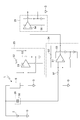
- FIG. 1 is a schematic block diagram illustrating a configuration of a semiconductor sample inspection apparatus according to the present embodiment.
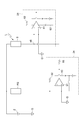
- FIG. 2 is a schematic diagram for describing measurement of electrical characteristics by the semiconductor sample inspection device.
- FIG. 3 is a schematic block diagram showing a configuration of a semiconductor sample inspection device according to a modification of the present embodiment.
- FIG. 4 is a schematic diagram for describing measurement of electrical characteristics by the semiconductor sample inspection device.
- FIG. 5 is a schematic block diagram illustrating a configuration of a semiconductor sample inspection device according to a modification of the present embodiment.
- FIG. 6 is a schematic diagram for explaining measurement of electrical characteristics by the semiconductor sample inspection device.
- FIG. 7 is a schematic block diagram illustrating a configuration of a semiconductor sample inspection device according to a modification of the present embodiment.
- FIG. 8 is a schematic diagram for explaining measurement of electrical characteristics by the semiconductor sample inspection device.
- FIG. 9 is a flowchart illustrating a method of inspecting a semiconductor sample.
- FIG. 10 is a flowchart
- FIG. 1 is a schematic block diagram of a semiconductor sample inspection apparatus according to the present embodiment.
- the semiconductor sample inspection apparatus 1 (hereinafter, simply referred to as an “inspection apparatus”) is an apparatus that inspects a semiconductor sample S, which is an object, for a defect using the OBIRCH method.
- the semiconductor sample S is, for example, a semiconductor member such as a semiconductor integrated circuit.
- a voltage is applied to the semiconductor sample S by the external power supply device 2, and based on a current signal output from the semiconductor sample S in response to the application of the voltage and the irradiation of light, a defect portion of the semiconductor sample S Will be inspected.
- This current signal is output by applying a voltage to the semiconductor sample S.
- the value of the current signal changes when the semiconductor sample S is irradiated with light.
- External power supply device 2 is, for example, a switching power supply.
- the inspection device 1 includes a light irradiation unit 10, an electrical characteristic measurement unit 20, and a control unit 30.
- the light irradiation unit 10 irradiates a semiconductor sample S to which a voltage is applied by the external power supply device 2 with light (for example, a laser beam L) to scan.
- a laser beam L is used as light to irradiate a semiconductor sample S.
- the light to be applied to the semiconductor sample S does not necessarily need to use coherent light, and may be, for example, incoherent light.
- the electric characteristic measuring unit 20 measures electric characteristics of the semiconductor sample S based on a current signal output from the semiconductor sample S to which a voltage is applied by the external power supply device 2 and irradiated with light.
- the control unit 30 controls the light irradiation unit 10 and the electrical property measurement unit 20.
- the control unit 30 outputs an inspection result of the semiconductor sample S based on the measured electric characteristics.
- the control unit 30 outputs an inspection result indicating a defective portion of the semiconductor sample S according to a change in electrical characteristics of the semiconductor sample S caused by light irradiation and scanning. As a result, the inspection apparatus 1 realizes inspection of a defective portion of the semiconductor sample S.
- the light irradiation unit 10 includes a laser source 11, a laser scanning unit 12, and a microscope 13.
- the laser source 11 is, for example, a semiconductor laser or a solid-state laser. When irradiating the semiconductor sample S with incoherent light, an SLD (Super Luminescent Diode) or an ASE light source may be used as the laser source 11.
- the laser generation source 11 generates and emits a laser beam.
- the laser scanning unit 12 is disposed on the optical path of the laser light emitted from the laser source 11. The laser beam emitted from the laser source 11 enters the laser scanning unit 12.
- the laser scanning unit 12 irradiates a laser beam incident through the microscope 13 as a laser beam L in a predetermined direction and performs scanning.
- the laser scanning unit 12 performs, for example, a raster scan (raster scan) in a two-dimensional direction orthogonal to the incident direction.
- the microscope 13 focuses the irradiated laser beam L to a small spot diameter.
- the microscope 13 acquires an image of the subject by the reflected light of the emitted laser beam L.
- the electrical characteristic measuring unit 20 includes sample tables 21 and 22, a test signal output unit 23, a reference signal output unit 24, a noise removal unit 25, an isolation unit 26, and an electrical characteristic measurement unit 27.
- a semiconductor sample S is placed on the sample table 21.
- the semiconductor sample S placed on the sample stage 21 is positioned at the focal position of the microscope 13.
- the reference member RS is placed on the sample stage 22.
- the reference member RS is, for example, a semiconductor member such as a semiconductor integrated circuit.
- the reference member RS has the same electrical characteristics as the semiconductor sample S. For example, the reference member RS has an impedance of ⁇ 30% with respect to the impedance of the semiconductor sample S.
- the reference member RS can be replaced with a reference member having different electric characteristics.
- the sample table 21 and the sample table 22 have an input terminal and an output terminal, respectively.
- the input terminals of the sample stage 21 and the sample stage 22 are electrically connected to the output terminal of the external power supply 2 in parallel with each other.
- the semiconductor sample S mounted on the sample stage 21 is electrically connected to the output terminal of the external power supply 2 through the sample stage 21.
- the semiconductor sample S is irradiated with the laser beam L and scanned by the light irradiation unit 10.
- the semiconductor sample S outputs a current signal resulting from a change in electrical characteristics of the semiconductor sample S due to the irradiation and scanning of the laser beam L, and an output of the external power supply device 2.
- the reference member RS placed on the sample stage 22 is connected to the output terminal of the external power supply device 2 via the sample stage 22. That is, the reference member RS is electrically connected to the external power supply device 2 in parallel with the semiconductor sample S.
- the reference member RS is not irradiated with the laser beam, and the electric characteristics do not change with the irradiation and scanning of the laser beam.
- the reference member RS outputs a current signal resulting from the output of the external power supply device 2.
- the test signal output unit 23 is electrically connected in series with the output terminal of the sample stage 21. That is, the test signal output unit 23 is connected in series to the external power supply 2 through the sample stage 21 and the semiconductor sample S.
- the test signal output unit 23 outputs a test signal based on the current signal output from the semiconductor sample S.
- the test signal output unit 23 includes a current-voltage conversion unit 43. The current signal input to the test signal output unit 23 is converted into a voltage signal by the current-voltage conversion unit 43. Therefore, the test signal is a voltage signal.
- the reference signal output unit 24 is electrically connected in series with the output terminal of the sample stage 22. That is, the reference signal output unit 24 is electrically connected in series to the reference member RS and the external power supply device 2.
- the reference signal output unit 24 is electrically connected to the external power supply 2 in parallel with the semiconductor sample S and the sample stage 22.
- the reference signal output unit 24 outputs a reference signal based on a current signal output from the reference member RS by applying a voltage from the external power supply device 2.
- the reference member RS is not irradiated with the laser beam, and the electric characteristics do not change with the irradiation and scanning of the laser beam. Therefore, the reference signal is a signal corresponding to the output of the external power supply device 2.
- the reference signal output unit 24 has a current-voltage conversion unit 44.
- the current-voltage converter 44 converts the current signal input to the reference signal output unit 24 into a voltage signal. Therefore, the reference signal is a voltage signal.
- the test signal output unit 23 and the reference signal output unit 24 in the present embodiment are each a negative feedback circuit having an operational amplifier 51, a resistor 52, and a floating circuit 53.
- the floating circuit 53 is connected to the ground G of the external power supply device 2 and forms a floating power supply.
- the operational amplifiers 51 of the test signal output unit 23 and the reference signal output unit 24 operate with the power supplied from the floating circuit 53.
- the ground G of the external power supply 2 and the semiconductor sample S are connected to the input terminal of the operational amplifier 51 of the test signal output unit 23.
- the test signal output unit 23 forms an inverting amplifier circuit in which the amplification factor changes according to the impedance change of the semiconductor sample S.
- the input terminal of the operational amplifier 51 of the reference signal output unit 24 is connected to the ground G of the external power supply 2 and the reference member RS.
- the reference signal output unit 24 constitutes an inverting amplifier circuit having an amplification factor based on the impedance of the reference member RS and the resistance value of the resistor 52.
- the noise removing unit 25 is electrically connected to the test signal output unit 23 and the reference signal output unit 24.
- the test signal and the reference signal are input to the noise removing unit 25.
- the noise removing unit 25 outputs a noise removing signal obtained by removing a noise component of the output of the external power supply device 2 from the current signal output from the semiconductor sample S based on the reference signal.
- the noise removing unit 25 has a differential detecting unit 45.
- the differential detection unit 45 outputs a signal including a difference between the test signal input to the noise removal unit 25 and the reference signal.
- the noise removing unit 25 outputs a signal including a difference between the test signal and the reference signal as a noise removing signal.
- the differential detection unit 45 includes, for example, a comparator 54 such as a comparator or an operational amplifier, and a floating circuit 55.
- the floating circuit 55 is connected to the ground G of the external power supply device 2 and forms a floating power supply.
- the comparator 54 operates with the power supplied from the floating circuit 55.
- the test signal output unit 23 and the reference signal output unit 24 are connected to the input terminal of the comparator 54. As a result, the difference between the test signal and the reference signal is output from the comparator 54.
- the isolation unit 26 connects the noise removing unit 25 and the electrical characteristic measuring unit 27 in an electrically insulated state.
- the noise removing unit 25 and the electrical characteristic measuring unit 27 are connected via the isolating unit 26.
- the isolating unit 26 converts the signal output from the noise removing unit 25 into a non-electric signal, converts the non-electric signal into an electric signal again, and outputs the electric signal to the electric characteristic measuring unit 27.
- the isolation unit 26 includes, for example, a transformer, a photocoupler, or a relay.
- the relay includes, for example, an electromagnetic switch.
- the isolating section 26 includes, for example, a transformer
- the isolating section 26 magnetically connects the noise removing section 25 and the electrical characteristic measuring section 27.
- the isolating section 26 includes, for example, a photocoupler
- the isolating section 26 optically connects the noise removing section 25 and the electrical characteristic measuring section 27.
- the electrical characteristic measuring unit 27 measures the electrical characteristics of the semiconductor sample S that change with the irradiation and scanning of the laser beam L, based on the noise removal signal transmitted from the noise removal unit 25 through the isolation unit 26. In the present embodiment, the electrical characteristic measuring unit 27 calculates a value indicating the impedance of the semiconductor sample S as the electrical characteristic of the semiconductor sample S from the noise removal signal at predetermined time intervals. The electric characteristic measuring unit 27 sequentially transmits the calculated electric characteristics (measurement results) to the control unit 30.
- the control unit 30 includes a system control unit 31 and a display unit 32.
- the system control unit 31 is connected to the laser scanning unit 12, the microscope 13, the electrical characteristic measuring unit 27, and the display unit 32.
- the system control unit 31 controls scanning of the laser beam L by the laser scanning unit 12, acquisition of an image of the semiconductor sample S by the microscope 13, operation of the electrical characteristic measurement unit 27, and display of the measurement result by the display unit 32.
- the system control unit 31 displays the state of the semiconductor sample S on the display unit 32 based on the measurement result output from the electrical characteristic measurement unit 27.
- the display unit 32 is, for example, a display such as a liquid crystal monitor.
- the system control unit 31 is physically a computer including a CPU (Central Processing Unit) as a processor, a RAM (Random Access Memory) and a ROM (Read Only Memory) as recording media, and a communication module. And input / output devices such as a mouse and a keyboard.
- the system control unit 31 may include a plurality of computers.
- the system control unit 31 irradiates the laser beam L to a fine portion on the surface of the semiconductor sample S by the light irradiation unit 10 and scans the laser beam L on the surface of the semiconductor sample S.
- a predetermined voltage is applied to the semiconductor sample S from the external power supply device 2, and a predetermined current flows in the circuit of the semiconductor sample S.
- the temperature of the portion increases due to the absorption of the energy of the laser beam L, and the impedance changes. Therefore, the value of the current flowing through the semiconductor sample S changes.
- the temperature rise is large when the laser beam L is irradiated.
- the current signal output from the semiconductor sample S is converted from the current signal into a voltage signal by the test signal output unit 23, amplified, and input to the noise removing unit 25 as a test signal.
- the current signal output from the reference member RS is converted from the current signal into a voltage signal by the reference signal output unit 24 and amplified, and is input to the noise removing unit 25 as a reference signal.
- the noise removing unit 25 amplifies and outputs a signal composed of a difference between the input test signal and the reference signal.
- the noise removal signal output from the noise removal unit 25 is input to the electrical characteristic measurement unit 27 via the isolation unit 26.
- the electrical characteristic measuring unit 27 measures the electrical characteristics of the semiconductor sample S at predetermined time intervals based on the input noise removal signal, and sequentially transmits the measurement results to the system control unit 31.
- the system control unit 31 converts the measurement result of the electrical characteristics of the semiconductor sample S into luminance information based on the measurement result transmitted from the electrical characteristics measurement unit 27.
- the system control unit 31 associates an irradiation position of the laser beam L with luminance information corresponding to the irradiation position.
- the system control unit 31 generates an image indicating a defective portion of the semiconductor sample S based on the irradiation position of the laser beam L and the luminance information, and displays the image on the display unit 32.
- the system control unit 31 outputs a defective portion of the semiconductor sample S based on the measurement result transmitted from the electrical characteristic measurement unit 27. Thereby, confirmation of a defective portion of the semiconductor sample S by an image is realized.
- the system control unit 31 generates an image based on the measurement results of the electrical characteristics acquired while irradiating and scanning the laser beam L over the entire measurement region on the surface of the semiconductor sample S, and generates the image. Is displayed on the display unit 32.
- FIG. 3 is a schematic block diagram of a semiconductor sample inspection device according to a modification of the present embodiment.
- FIG. 4 is a schematic view showing a part of the semiconductor sample inspection apparatus.
- the modified example shown in FIGS. 3 and 4 is different from the above-described embodiment in that a DC component cut section is provided instead of the sample table 22 and the reference member RS.
- a DC component cut section is provided instead of the sample table 22 and the reference member RS.
- the electrical characteristic measuring unit 20 of the inspection apparatus 1A includes a sample table 21, a test signal output unit 23, a reference signal output unit 24, a noise removing unit 25, an isolating unit 26, an electrical characteristic measuring unit 27, and a DC component cutting unit 28. Is provided.
- the input of the DC component cut section 28 is connected to the output terminal of the external power supply 2 electrically in parallel with the sample stage 21.
- the output of the DC component cut unit 28 is connected to the reference signal output unit 24. That is, the reference signal output unit 24 is connected in series to the external power supply device 2 with the DC component cut unit 28 interposed therebetween.
- the ⁇ DC component cut unit 28 outputs a signal obtained by removing a DC current component from a current signal output from the external power supply device 2.
- the reference signal output unit 24 outputs a reference signal based on the signal output from the DC component cut unit 28.
- the reference signal output unit 24 outputs, as a reference signal, a signal obtained by removing a DC current component from a current signal output from the external power supply device 2.
- the signal input to the reference signal output unit 24 is converted into a voltage signal by the current / voltage conversion unit 44. Therefore, the reference signal is a voltage signal.
- the DC component cut unit 28 in the present embodiment has a capacitor 56.
- the capacitor 56 is connected to the output terminal of the external power supply 2 electrically in parallel with the semiconductor sample S.
- the capacitor 56 is electrically connected to the reference signal output unit 24 in series.
- the reference signal output unit 24 in the present modification has a resistor 57 in addition to the operational amplifier 51, the resistor 52, and the floating circuit 53, and these constitute an inverting amplifier circuit.
- a signal obtained by removing a DC current component from a current signal output from the external power supply device 2 by the DC component cut unit 28 is input to the reference signal output unit 24.
- the AC component of the current signal output from the external power supply device 2 that is, the noise component is input to the reference signal output unit 24. Therefore, the reference signal output from the reference signal output unit 24 is a signal indicating normal noise.
- the current signal output from the semiconductor sample S is converted from the current signal into a voltage signal by the test signal output unit 23, amplified, and input to the noise removing unit 25 as a test signal.
- the current signal output from the DC component cut unit 28 is converted from the current signal into a voltage signal by the reference signal output unit 24, amplified, and input to the noise removal unit 25 as a reference signal.
- the noise removing unit 25 amplifies and outputs a signal consisting of a difference between the input test signal and the reference signal.
- FIG. 5 is a schematic block diagram of a semiconductor sample inspection device according to a modification of the present embodiment.
- FIG. 6 is a schematic view showing a part of a semiconductor sample inspection apparatus.
- the modification shown in FIGS. 5 and 6 is different from the first embodiment in that the noise elimination unit does not have a current-to-voltage conversion unit before the noise elimination unit.
- This embodiment differs from the above-described embodiment in that the addition is performed.
- differences from the above-described embodiment will be mainly described.
- the test signal output unit 23 includes only wiring for electrically connecting the output terminal of the sample stage 21 and the noise removing unit 25 in series. That is, the test signal output unit 23 inputs the current signal output from the semiconductor sample S to the noise removal unit 25 as a test signal. Therefore, the test signal is a current signal.
- the reference signal output unit 24 has an inverted gain adjustment unit 47.
- the inverting gain adjustment unit 47 converts the current signal input to the reference signal output unit 24, that is, the current signal corresponding to the output of the external power supply device, into an opposite phase, and the gain is adjusted according to the gain of the test signal.
- the reference signal is output. Therefore, the reference signal is a current signal having a phase opposite to that of the current signal output from the reference member RS.
- the reference signal output unit 24 in the present modification is a negative feedback circuit having a resistor 58 in addition to the operational amplifier 51, the resistor 52, and the floating circuit 53.
- the floating circuit 53 is connected to the ground G of the external power supply device 2 and forms a floating power supply.
- the operational amplifier 51 of the reference signal output unit 24 operates by the power supplied from the floating circuit 53.
- the ground G of the external power supply 2 and the reference member RS are connected to the input terminal of the operational amplifier 51 of the reference signal output unit 24.
- the reference signal output unit 24 constitutes an inverting amplifier circuit having an amplification factor based on the impedance of the reference member RS and the resistance value of the resistor 52.
- the resistor 58 adjusts the gain of the reference signal output from the reference signal output unit 24.
- the noise removing unit 25 includes an adding unit 48 and a current-voltage converting unit 49 (amplifying unit).
- the adder 48 adds the test signal and the reference signal and outputs the result to the current-voltage converter 49.
- the adder 48 is connected to the wiring (test signal output unit 23) connected to the output terminal of the sample stage 21 and the reference signal output unit 24, as shown in FIG.
- This is a connector for connecting the wiring and the current-voltage converter 49. That is, the adding section 48 outputs a current signal having a current value obtained by adding the current value of the test signal and the current value of the reference signal.
- the current-voltage converter 49 converts the current signal output from the adder 48 into a voltage signal and amplifies it. Therefore, the noise removal signal output from the noise removal unit 25 is a voltage signal.
- the current-voltage converter 49 in the present modification is a negative feedback circuit having an operational amplifier 61, a resistor 62, and a floating circuit 63.
- the floating circuit 63 is connected to the ground G of the external power supply device 2 and forms a floating power supply.
- the operational amplifier 61 operates with power supplied from the floating circuit 63.
- the input terminal of the operational amplifier 61 is connected to the ground G of the external power supply 2 and the adder 48.
- the current-voltage converter 49 forms an inverting amplifier circuit.
- the current signal output from the semiconductor sample S is input to the noise removing unit 25 as a test signal.
- the current signal output from the reference member RS is converted into a current signal of opposite phase by the reference signal output unit 24, and is input to the noise removal unit 25 as a reference signal.
- the noise removing unit 25 the test signal and the reference signal are added by the adding unit 48, and converted into a voltage signal and amplified by the current-voltage converting unit 49.
- FIG. 7 is a schematic block diagram of a semiconductor sample inspection device according to a modification of the present embodiment.
- FIG. 8 is a schematic view showing a part of a semiconductor sample inspection apparatus.
- the modification shown in FIGS. 7 and 8 is different from the modification shown in FIGS. 5 and 6 in that a DC component cut section 28 is provided instead of the sample table 22 and the reference member RS. Different.
- differences from the modification shown in FIGS. 5 and 6 will be mainly described.
- the electric characteristic measuring unit 20 includes a sample table 21, a signal output unit 23, a reference signal output unit 24, a noise removing unit 25, an isolating unit 26, an electric characteristic measuring unit 27, and a DC component cutting unit 28. Is provided.
- the input of the DC component cut section 28 is connected to the output terminal of the external power supply 2 electrically in parallel with the sample stage 21.
- the output of the DC component cut unit 28 is connected to the reference signal output unit 24. That is, the reference signal output unit 24 is connected in series to the external power supply device 2 via the DC component cut unit 28.
- the ⁇ DC component cut unit 28 outputs a signal obtained by removing a DC current component from a current signal output from the external power supply device 2.
- the reference signal output unit 24 outputs a reference signal based on the signal output from the DC component cut unit 28.
- the signal input to the reference signal output unit 24 is converted into a voltage signal by the current / voltage conversion unit 44. Therefore, the reference signal is a voltage signal.
- the DC component cut unit 28 in the present embodiment has a capacitor 56.
- the capacitor 56 is connected to the output terminal of the external power supply 2 electrically in parallel with the semiconductor sample S.
- the capacitor 56 is electrically connected to the reference signal output unit 24 in series.
- the reference signal output unit 24 in this modification has resistors 57 and 58 in addition to the operational amplifier 51, the resistor 52, and the floating circuit 53, and these constitute an inverting amplifier circuit.
- a signal obtained by removing a DC current component from a current signal output from the external power supply device 2 by the DC component cut unit 28 is input to the reference signal output unit 24.
- the AC component of the current signal output from the external power supply device 2 is input to the reference signal output unit 24.
- the AC component corresponds to a noise component. Therefore, the reference signal output from the reference signal output unit 24 is a signal indicating normal noise.
- the current signal output from the semiconductor sample S is input to the noise removing unit 25 as a test signal.
- the current signal output from the DC component cut unit 28 is converted into a current signal of opposite phase by the reference signal output unit 24, and is input to the noise removal unit 25 as a reference signal.
- the noise removing unit 25 adds the test signal and the reference signal by the adding unit 48, converts the signal into a voltage signal by the current-voltage converting unit 49, amplifies and outputs the voltage signal.
- FIG. 9 is a flowchart illustrating a method of inspecting a semiconductor sample.
- FIG. 10 is a flowchart showing the details of the electrical characteristic measurement processing of the processing shown in FIG.
- the semiconductor sample S and the reference member RS or the capacitor 56 are prepared (process S1).
- the semiconductor sample S is placed on the sample table 21 and connected to the external power supply 2.
- the reference member RS is placed on the sample stage 22, is connected to the external power supply 2 electrically in parallel with the semiconductor sample S, and is electrically connected in series to the reference signal. Connected to output unit 24.
- the capacitor 56 is electrically connected to the external power supply 2 in parallel with the semiconductor sample S, and is electrically connected to the reference signal output unit 24 in series.
- the capacitor 56 may be connected to the reference signal output unit 24 in advance. When the capacitor 56 is connected to the reference signal output unit 24 in advance, the processing shown in the processing S1 is omitted.
- process S2 the application of the voltage to the semiconductor sample S by the external power supply device 2 is started (process S2).
- the application of the voltage to the reference member RS by the external power supply device 2 is also started.
- the application of the voltage by the external power supply device 2 is continued until all processes are completed.
- process S3 irradiation of the semiconductor sample S with the laser beam L and scanning by the light irradiation unit 10 are started (process S3).
- the irradiation and scanning of the laser beam L on the semiconductor sample S by the light irradiation unit 10 are continued until the entire measurement region of the semiconductor sample S is irradiated and scanned with the laser beam L.
- process S4 a measurement process of electrical characteristics is performed.
- the measurement results of the electric characteristics measured by the electric characteristic measurement unit 20 are sequentially transmitted to the system control unit 31.
- the measurement result of the electrical characteristics is displayed on the display unit 32 by the system control unit 31 (process S5).
- the system control unit 31 measures the electric characteristics of the semiconductor sample S corresponding to the irradiation position of the laser beam L based on the measurement result transmitted from the electric characteristic measurement unit 27 and the irradiation position of the laser beam L. Convert the result to luminance information. Subsequently, the system control unit 31 associates the irradiation position of the laser beam L with luminance information corresponding to the irradiation position.
- the system control unit 31 generates an image indicating a defective portion of the semiconductor sample S based on the irradiation position of the laser beam L and the luminance information, and displays the image on the display unit 32. That is, the system control unit 31 outputs a defective portion of the semiconductor sample S based on the measurement result transmitted from the electrical characteristic measurement unit 27.
- step S6 determines whether or not to end all the processes. If it is determined that the processing is not to be ended (NO in step S6), the process returns to the step S3, and irradiation with the laser beam L and scanning are started. If it is determined that the processing is to be ended (YES in step S6), all the processing ends.
- the reference signal and the test signal are acquired by the noise removing unit 25 (processing S41).
- the test signal is a signal based on a current signal output from the semiconductor sample S in response to application of a voltage from the external power supply device 2.
- the test signal is a signal obtained by converting a current signal output from the semiconductor sample S into a voltage signal in response to application of a voltage from the external power supply device 2.
- the test signal is the current signal itself output from the semiconductor sample S in response to the application of the voltage from the external power supply device 2.
- the reference signal is a signal output in response to the output of the external power supply 2 from the reference signal output unit 24 connected to the external power supply 2 electrically in parallel with the semiconductor sample S.
- the reference signal is a signal based on the current signal output from the reference member RS due to the output of the external power supply device 2.
- the reference signal is a signal output from the reference signal output unit 24 based on a signal obtained by removing a DC current component from a current signal output from the external power supply device 2.
- the signal obtained by removing the DC current component from the current signal output from the external power supply device 2 is generated by, for example, the capacitor 56.
- the reference signal is a voltage signal corresponding to the output of the external power supply device 2.
- the reference signal is a signal in which the current signal output from the reference member RS or the DC component cut unit 28 has an opposite phase according to the output of the external power supply device 2.
- the noise removal unit 25 generates a noise removal signal in which noise of the output of the external power supply device 2 has been removed from the test signal based on the reference signal (process S42).
- the noise removal unit 25 When using the inspection devices 1 and 1A, the noise removal unit 25 generates a noise removal signal based on the difference between the reference signal and the test signal.
- the noise removal unit 25 When the inspection devices 1B and 1C are used, the noise removal unit 25 generates a noise removal signal by adding and amplifying the reference signal and the test signal.
- the electrical characteristic measurement unit 27 measures the electrical characteristics of the semiconductor sample S based on the noise removal signal generated by the noise removal unit 25. In the present embodiment, the electrical characteristic measurement unit 27 sequentially transmits the measurement results to the system control unit 31.
- step S44 it is determined whether to terminate the electrical characteristic measurement process. If it is determined that the processing is not to be terminated (NO in step S44), the process returns to step S41, and the noise elimination unit 25 acquires the reference signal and the test signal. If it is determined that the processing is to be terminated (YES in step S44), the measurement processing of the electrical characteristics is terminated, and the process proceeds to step S5.
- the inspection apparatuses 1, 1 ⁇ / b> A, 1 ⁇ / b> B, and 1 ⁇ / b> C according to the present embodiment and the modifications are connected to the external power supply 2 electrically in parallel with the semiconductor sample S, and A reference signal output unit 24 that outputs a reference signal according to the output is provided.
- the noise removal unit 25 removes noise of the output of the external power supply device 2 from the test signal indicating the current signal output from the semiconductor sample S by application of the voltage by the external power supply device 2 based on the reference signal. Output a signal.
- the electric characteristic measuring unit 27 measures electric characteristics of the semiconductor sample S based on the noise removal signal.
- the power supplied to the semiconductor sample S using the external power supply device 2 is improved, and the influence of noise on the measurement results of the electrical characteristics of the semiconductor sample S is reduced. Reduction can be achieved at the same time. As a result, the inspection accuracy of the defect location of the semiconductor sample S can be improved.
- the reference signal output unit 24 is electrically connected in series to the reference member RS connected to the external power supply device 2 in parallel with the semiconductor sample S.
- the reference signal output unit 24 outputs a signal based on the current signal output from the reference member RS by applying a voltage from the external power supply device 2 as a reference signal.
- the reference signal output by the reference signal output unit 24 is based on a current signal from the reference member RS connected to the external power supply device 2 in parallel with the semiconductor sample S. For this reason, it is easy to adjust the gain of the reference signal in accordance with the current signal output from the semiconductor sample S.
- the reference signal output unit 24 outputs, as a reference signal, a signal obtained by removing a DC current component from a current signal output from the external power supply device 2.
- the reference signal output from the reference signal output unit 24 is based on a signal obtained by removing a DC current component from a current signal output from the external power supply device 2.
- the signal from which the direct current component has been removed indicates a noise component of the output of the external power supply device 2. Therefore, it is easy to generate the reference signal including the noise component of the output of the external power supply device 2.
- the capacitor 56 is connected to the external power supply device 2 in parallel with the semiconductor sample S. Therefore, all the DC components of the current signal output from the external power supply device 2 are input to the test signal output unit 23 through the semiconductor sample S. That is, the current value output from the external power supply device 2 is the current value output from the semiconductor sample S. As a result, the easiness of measuring the electric characteristics is improved.
- the test signal output unit 23 outputs a test signal obtained by converting a current signal output from the semiconductor sample S into a voltage signal.
- the reference signal output unit 24 outputs a signal obtained by converting a current signal from the external power supply 2 into a voltage signal as a reference signal.
- the noise removing unit 25 outputs a signal including a difference between the test signal and the reference signal as a noise removing signal. In this case, in the noise removal signal composed of the difference between the test signal and the reference signal, noise generated when converting the current signal to the voltage signal is also removed.
- the reference signal output unit 24 outputs, as a reference signal, a signal obtained by inverting the phase of a current signal corresponding to the output of the external power supply device 2.
- the adder 48 adds the reference signal to the current signal output from the semiconductor sample S.
- the current-voltage converter 49 amplifies the signal added by the adder 48. In this case, amplification is performed after adding the reference signal to the current signal output from the semiconductor sample S. That is, amplification is performed after noise of the output of the external power supply device 2 is removed. For this reason, even when the noise of the output of the external power supply device 2 is large, it is possible to prevent the noise from being removed from the reference signal due to the saturation due to the amplification. Therefore, the noise of the output of the external power supply device 2 is more accurately removed.
- the noise removing unit 25 and the electrical characteristic measuring unit 27 are electrically insulated by the isolating unit 26.
- the isolation unit 26 connects the noise elimination unit 25 and the electrical characteristic measurement unit 27 via, for example, a transformer, a photocoupler, or a relay. In this case, it is possible to prevent the common mode noise from being mixed into the electrical characteristic measuring section.
- At least one of the reference signal output unit 24 and the noise removal unit 25 operates by power supplied from the floating circuit 63 connected to the ground G of the external power supply 2. In this case, mixing of common mode noise from a power supply that supplies power to the reference signal output unit 24 or the noise removal unit 25 is suppressed.
- the electric characteristic measuring unit 27 and the system control unit 31 are described separately, but the electric characteristic measuring unit 27 may be included in the system control unit 31.
- the system control unit 31 may display an image on the display unit 32 after irradiating and scanning the entire or predetermined portion of the measurement region of the semiconductor sample S with the laser beam L, or may display a measurement result from the electrical characteristic measurement unit 27. Images may be sequentially displayed on the display unit 32 in response to the reception.
- the electrical characteristic measurement unit 27 sequentially transmits the measurement results to the system control unit 31.
- the system control unit 31 After irradiating and scanning the laser beam L on all or a predetermined portion of the measurement area of the semiconductor sample S, the system control unit 31 The measurement results may be transmitted to the group 31 in a lump.
- the processing flow described in the present embodiment describes an exemplary processing order, and the present inspection method is not limited to the specific processing order described.
- the processing order may be changed as long as there is no contradiction. For example, the start of the application of the voltage to the semiconductor sample S by the external power supply device 2 and the start of the irradiation and scanning of the laser beam L to the semiconductor sample S by the light irradiation unit 10 may be reversed.
- 1, 1A, 1B, 1C Inspection device
- 2 External power supply device
- 23 Test signal output unit
- 24 Reference signal output unit
- 25 Noise removal unit
- 26 Isolate unit
- 27 Electrical characteristic measurement unit .., 48...
- An adder 49.
- a capacitor 63.
- a floating circuit S.
Abstract
This inspection device 1 comprises a reference signal output unit 24, a noise removal unit 25, and an electrical characteristic measurement unit 27. The reference signal output unit 24 is electrically connected, in parallel with a semiconductor sample S, to an external power supply device 2 and outputs a reference signal corresponding to the output of the external power supply device 2. A noise removal unit 25 outputs a noise-removed signal produced by using the reference signal to remove the noise component of the output of the external power supply device 2 from a current signal output from the semiconductor sample S. An electrical characteristic measurement unit 27 measures an electrical characteristic of the semiconductor sample S on the basis of the noise-removed signal. The inspection device 1 measures the electrical characteristic of the semiconductor sample S while the same is having a voltage applied thereto by the external power supply device 2 and is being scanned with emitted light. The inspection device 1 outputs a defective location of the semiconductor sample S on the basis of the electrical characteristic.
Description
本発明は、半導体試料の検査装置及び検査方法に関する。
The present invention relates to an inspection apparatus and an inspection method for a semiconductor sample.
OBIRCH(Optical Beam Induced Resistance Change)法を用いて、半導体試料の欠陥箇所を検査する半導体試料の検査装置が知られている(たとえば、特許文献1)。検査装置は、半導体試料に電圧を印加し、半導体試料から出力された電流信号に基づいて、レーザビームの照射及び走査に伴う半導体試料の電気特性を測定する。検査装置は、測定された電気特性に基づいて、半導体試料の欠陥箇所を検査する。
2. Description of the Related Art A semiconductor sample inspection apparatus for inspecting a defect portion of a semiconductor sample using an OBIRCH (Optical Beam Induced Resistance Change) method is known (for example, Patent Document 1). The inspection apparatus applies a voltage to the semiconductor sample, and measures electrical characteristics of the semiconductor sample accompanying the irradiation and scanning of the laser beam based on a current signal output from the semiconductor sample. The inspection device inspects a defective portion of the semiconductor sample based on the measured electrical characteristics.
OBIRCH法を用いた半導体試料の検査装置では、半導体試料から出力される電流信号の強度が向上されれば、レーザビームの照射及び走査に伴う半導体試料の電気特性の変化量が向上する。この電気特性の変化量が向上するほど、半導体試料の欠陥箇所の検査精度も向上する。このため、半導体試料に供給する電力の向上が求められている。しかしながら、OBIRCH法を用いた検査装置では、レーザビームの照射及び走査、顕微鏡部の動作、並びに測定結果の画像処理などの様々な機能に電力を要する。このため、半導体試料に供給できる電力は限られている。
In an inspection apparatus for a semiconductor sample using the IROBIRCH method, if the intensity of a current signal output from the semiconductor sample is improved, the amount of change in electrical characteristics of the semiconductor sample due to laser beam irradiation and scanning is improved. As the amount of change in the electrical characteristics is improved, the inspection accuracy of a defective portion of the semiconductor sample is also improved. For this reason, improvement in the power supplied to the semiconductor sample is required. However, in an inspection apparatus using the OBIRCH method, power is required for various functions such as irradiation and scanning of a laser beam, operation of a microscope unit, and image processing of a measurement result. For this reason, the power that can be supplied to the semiconductor sample is limited.
半導体試料に供給する電力を向上するために、検査装置の内部電源ではなく、外部電源装置から半導体試料に電力を供給することが考えられる。しかしながら、外部電源装置を用いた場合、半導体試料から出力される電流信号に外部電源装置に起因するノーマルモードノイズ(たとえば、スイッチングノイズ)が混入するおそれがある。半導体試料から出力される電流信号にノイズが混入すれば、半導体試料の電気特性の測定結果にもノイズの影響が及ぶ。このため、外部電源装置によって半導体試料に供給される電力が向上したとしても、ノイズの影響でかえって半導体試料の欠陥箇所の検査精度が低下するおそれがある。
In order to improve the power supplied to the semiconductor sample, it is conceivable to supply power to the semiconductor sample from an external power supply device instead of the internal power supply of the inspection apparatus. However, when an external power supply is used, there is a possibility that normal mode noise (for example, switching noise) due to the external power supply may be mixed in a current signal output from the semiconductor sample. If noise is mixed in the current signal output from the semiconductor sample, the noise affects the measurement result of the electrical characteristics of the semiconductor sample. For this reason, even if the power supplied to the semiconductor sample by the external power supply device is improved, the inspection accuracy of the defective portion of the semiconductor sample may be reduced due to the influence of noise.
本発明の一つの態様は、半導体試料の欠陥箇所の検査精度を向上できる半導体試料の検査装置を提供することを目的とする。本発明の別の態様は、半導体試料の欠陥箇所の検査精度を向上できる半導体試料の検査方法を提供することを目的とする。
An object of one embodiment of the present invention is to provide a semiconductor sample inspection apparatus capable of improving the inspection accuracy of a defect portion of a semiconductor sample. Another object of the present invention is to provide a method for inspecting a semiconductor sample which can improve the inspection accuracy of a defective portion of the semiconductor sample.
本発明の一つの態様に係る半導体試料の検査装置は、参照信号出力部と、ノイズ除去部と、電気特性測定部とを備える。参照信号出力部は、半導体試料と電気的に並列に外部電源装置に接続されている。参照信号出力部は、外部電源装置の出力に応じた参照信号を出力する。ノイズ除去部は、参照信号に基づいて、外部電源装置による電圧の印加によって半導体試料から出力された電流信号から外部電源装置の出力のノイズ成分を除去したノイズ除去信号を出力する。電気特性測定部は、ノイズ除去信号に基づいて、半導体試料の電気特性を測定する。検査装置は、外部電源装置によって電圧が印加されていると共に光が照射及び走査されている半導体試料の電気特性を測定し、当該電気特性に基づいて半導体試料の欠陥箇所を出力する。
半導体 A semiconductor sample inspection apparatus according to one aspect of the present invention includes a reference signal output unit, a noise removal unit, and an electrical characteristic measurement unit. The reference signal output unit is electrically connected to the external power supply in parallel with the semiconductor sample. The reference signal output section outputs a reference signal according to the output of the external power supply. The noise removal unit outputs a noise removal signal obtained by removing a noise component of an output of the external power supply from a current signal output from the semiconductor sample by applying a voltage from the external power supply based on the reference signal. The electrical property measurement unit measures electrical properties of the semiconductor sample based on the noise removal signal. The inspection apparatus measures an electrical characteristic of a semiconductor sample to which a voltage is applied by an external power supply device and is irradiated and scanned with light, and outputs a defective portion of the semiconductor sample based on the electrical characteristic.
上記一つの態様では、検査装置は、半導体試料と電気的に並列に外部電源装置と接続されていると共に、外部電源装置の出力に応じた参照信号を出力する参照信号出力部を備えている。ノイズ除去部は、当該参照信号に基づいて、外部電源装置による電圧の印加によって半導体試料から出力された電流信号を示す被検信号から外部電源装置の出力のノイズを除去したノイズ除去信号を出力する。電気特性測定部は、ノイズ除去信号に基づいて、半導体試料の電気特性を測定する。このため、上記検査装置では、外部電源装置を用いて半導体試料に供給する電力を向上することと、半導体試料の電気特性の測定結果に及ぶノイズの影響を低減することとを両立することができる。この結果、半導体試料の欠陥箇所の検査精度が向上され得る。
In one aspect, the inspection apparatus is electrically connected to the external power supply in parallel with the semiconductor sample, and includes a reference signal output unit that outputs a reference signal according to the output of the external power supply. The noise removal unit outputs a noise removal signal obtained by removing noise of an output of the external power supply from a test signal indicating a current signal output from the semiconductor sample by application of a voltage from the external power supply, based on the reference signal. . The electrical property measurement unit measures electrical properties of the semiconductor sample based on the noise removal signal. For this reason, in the inspection device, it is possible to improve the power supplied to the semiconductor sample using the external power supply device and reduce the influence of noise on the measurement result of the electrical characteristics of the semiconductor sample. . As a result, the inspection accuracy of a defective portion of the semiconductor sample can be improved.
上記一つの態様では、参照信号出力部は、半導体試料と電気的に並列に外部電源装置に接続された参照部材に電気的に直列に接続されていてもよい。参照信号出力部は、外部電源装置による電圧の印加によって参照部材から出力された電流信号に基づく信号を参照信号として出力してもよい。この場合、参照信号出力部が出力する参照信号は、半導体試料と電気的に並列に外部電源装置と接続された参照部材からの電流信号に基づく。このため、半導体試料から出力された電流信号に合わせて、参照信号のゲインを調整することが容易である。
In one aspect described above, the reference signal output unit may be electrically connected in series to the reference member connected to the external power supply in electrical parallel with the semiconductor sample. The reference signal output unit may output, as a reference signal, a signal based on the current signal output from the reference member by applying a voltage from the external power supply device. In this case, the reference signal output from the reference signal output unit is based on a current signal from a reference member that is electrically connected to the external power supply in parallel with the semiconductor sample. For this reason, it is easy to adjust the gain of the reference signal in accordance with the current signal output from the semiconductor sample.
上記一つの態様では、参照信号出力部は、外部電源装置から出力された電流信号から直流電流成分が除去された信号を参照信号として出力してもよい。この場合、参照信号出力部が出力する参照信号は、外部電源装置から出力された電流信号から直流電流成分を除去した信号に基づく。直流電流成分が除去された信号は、外部電源装置の出力のノイズ成分を示す。このため、外部電源装置の出力のノイズ成分を含む参照信号の生成が容易である。
In one aspect, the reference signal output unit may output, as the reference signal, a signal obtained by removing a DC current component from the current signal output from the external power supply device. In this case, the reference signal output from the reference signal output unit is based on a signal obtained by removing a DC current component from a current signal output from the external power supply device. The signal from which the direct current component has been removed indicates a noise component of the output of the external power supply. Therefore, it is easy to generate the reference signal including the noise component of the output of the external power supply device.
上記一つの態様では、半導体試料と電気的に並列に外部電源装置に接続されていると共に、参照信号出力部と電気的に直列に接続されたコンデンサを更に備えていてもよい。この場合、当該コンデンサが半導体試料と電気的に並列に前記外部電源装置と接続されているため、外部電源装置から出力される電流値が半導体試料から出力される電流値である。この結果、電気特性測定の容易性が向上する。
In the above aspect, the semiconductor device may further include a capacitor electrically connected in parallel with the semiconductor sample to the external power supply device and electrically connected in series with the reference signal output unit. In this case, since the capacitor is electrically connected to the external power supply in parallel with the semiconductor sample, the current value output from the external power supply is the current value output from the semiconductor sample. As a result, the easiness of measuring the electric characteristics is improved.
上記一つの態様では、半導体試料から出力された電流信号を電圧信号に変換した被検信号を出力する被検信号出力部を備えていてもよい。参照信号出力部は、外部電源装置からの電流信号を電圧信号に変換した信号を参照信号として出力してもよい。ノイズ除去部は、被検信号と参照信号との差分からなる信号をノイズ除去信号として出力してもよい。この場合、被検信号生成部と参照信号出力部とのそれぞれにおいて電流信号を電圧信号に変換させることで、被検信号と参照信号とを得る。このため、被検信号と参照信号との差分からなるノイズ除去信号では、電流信号から電圧信号に変換させる際に生じるノイズも除去されている。
In one aspect described above, a test signal output unit that outputs a test signal obtained by converting a current signal output from a semiconductor sample into a voltage signal may be provided. The reference signal output unit may output a signal obtained by converting a current signal from the external power supply into a voltage signal as a reference signal. The noise elimination unit may output a signal including a difference between the test signal and the reference signal as a noise elimination signal. In this case, a test signal and a reference signal are obtained by converting a current signal into a voltage signal in each of the test signal generation unit and the reference signal output unit. For this reason, in the noise removal signal composed of the difference between the test signal and the reference signal, noise generated when converting the current signal to the voltage signal is also removed.
上記一つの態様では、参照信号出力部は、外部電源装置の出力に応じた電流信号を逆相にした信号を参照信号として出力してもよい。ノイズ除去部は、加算部と増幅部とを有していてもよい。加算部は、半導体試料から出力された電流信号に参照信号を加算してもよい。増幅部は、加算部によって加算された信号を増幅してもよい。この場合、半導体試料から出力された電流信号に参照信号を加算した後に増幅が行われる。すなわち、外部電源装置の出力のノイズが除去された後に増幅が行われる。このため、外部電源装置の出力のノイズが大きい場合でも、増幅による飽和によって参照信号からノイズが除去されてしまうことを防止できる。したがって、外部電源装置の出力のノイズがより正確に除去される。
In one aspect described above, the reference signal output unit may output, as a reference signal, a signal in which a current signal corresponding to the output of the external power supply device is inverted in phase. The noise removing unit may include an adding unit and an amplifying unit. The adding unit may add the reference signal to the current signal output from the semiconductor sample. The amplification unit may amplify the signal added by the addition unit. In this case, amplification is performed after adding the reference signal to the current signal output from the semiconductor sample. That is, amplification is performed after noise of the output of the external power supply device is removed. Therefore, even when the noise of the output of the external power supply device is large, it is possible to prevent the noise from being removed from the reference signal due to the saturation due to the amplification. Therefore, the noise of the output of the external power supply device is more accurately removed.
上記一つの態様では、ノイズ除去部と電気特性測定部とは、電気的に絶縁され、トランス、フォトカプラ、又はリレーを介して接続されていてもよい。この場合、電気特性測定部にコモンモードノイズが混入することを防止できる。
In one aspect, the noise elimination unit and the electrical property measurement unit may be electrically insulated and connected via a transformer, a photocoupler, or a relay. In this case, it is possible to prevent the common mode noise from being mixed into the electrical characteristic measuring section.
上記一つの態様では、参照信号出力部及びノイズ除去部の少なくとも一つは、外部電源装置のグラウンドと接続されたフローティング回路から供給される電力によって動作してもよい。この場合、参照信号出力部又はノイズ除去部に電力を供給する電源からのコモンモードノイズの混入が抑制される。
In one aspect, at least one of the reference signal output unit and the noise removal unit may operate with power supplied from a floating circuit connected to the ground of the external power supply device. In this case, mixing of common mode noise from a power supply that supplies power to the reference signal output unit or the noise removal unit is suppressed.
本発明の別の態様に係る半導体試料の検査方法は、外部電源装置によって半導体試料に電圧が印加される。外部電源装置によって電圧が印加されている半導体試料に対して、光が照射及び走査される。外部電源装置による電圧の印加に応じて半導体試料から出力された電流信号に基づく被検信号が取得される。半導体試料と電気的に並列に外部電源装置に接続された参照信号出力部から外部電源装置の出力に応じて出力された参照信号が取得される。参照信号に基づいて、被検信号から外部電源装置の出力のノイズを除去したノイズ除去信号が生成される。ノイズ除去信号に基づいて、半導体試料の電気特性が測定される。半導体試料の電気特性に基づいて、半導体試料の欠陥箇所が出力される。
In the semiconductor sample inspection method according to another aspect of the present invention, a voltage is applied to the semiconductor sample by an external power supply device. The semiconductor sample to which a voltage is applied by the external power supply device is irradiated with light and scanned. A test signal is obtained based on the current signal output from the semiconductor sample in response to the application of the voltage by the external power supply. A reference signal output according to the output of the external power supply is obtained from a reference signal output unit electrically connected to the external power supply in parallel with the semiconductor sample. Based on the reference signal, a noise removal signal is generated by removing noise from the output of the external power supply from the test signal. The electrical characteristics of the semiconductor sample are measured based on the noise removal signal. A defect portion of the semiconductor sample is output based on the electrical characteristics of the semiconductor sample.
上記別の態様では、半導体試料と電気的に並列に外部電源装置に接続された参照信号出力部から外部電源装置の出力に応じた参照信号が取得される。この参照信号に基づいて、被検信号から外部電源装置の出力のノイズが除去される。被検信号からノイズが除去されたノイズ除去信号に基づいて、半導体試料の電気特性が測定される。このため、上記検査装置では、外部電源装置を用いて半導体試料に供給する電力を向上することと、半導体試料の電気特性の測定結果に及ぶノイズの影響を低減することとを両立することができる。この結果、半導体試料の欠陥箇所の検査精度が向上され得る。
In the another aspect, the reference signal corresponding to the output of the external power supply is obtained from the reference signal output unit connected to the external power supply electrically in parallel with the semiconductor sample. Based on the reference signal, noise of the output of the external power supply is removed from the test signal. The electrical characteristics of the semiconductor sample are measured based on the noise-removed signal obtained by removing noise from the test signal. For this reason, in the inspection device, it is possible to improve the power supplied to the semiconductor sample using the external power supply device and reduce the influence of noise on the measurement result of the electrical characteristics of the semiconductor sample. . As a result, the inspection accuracy of a defective portion of the semiconductor sample can be improved.
上記別の態様では、外部電源装置に半導体試料と電気的に並列に、かつ、参照信号出力部に電気的に直列に、参照部材を接続してもよい。参照信号は、外部電源装置による電圧の印加によって参照部材から出力された電流信号に基づく信号であってもよい。この場合、参照信号は、半導体試料と電気的に並列に外部電源装置と接続された参照部材からの電流信号に基づく。このため、半導体試料から出力された電流信号に合わせて、参照信号のゲインを調整することが容易である。
In the another aspect, the reference member may be connected to the external power supply device electrically in parallel with the semiconductor sample and electrically connected in series to the reference signal output unit. The reference signal may be a signal based on a current signal output from the reference member by applying a voltage from the external power supply device. In this case, the reference signal is based on a current signal from a reference member that is electrically connected to the external power supply in parallel with the semiconductor sample. For this reason, it is easy to adjust the gain of the reference signal in accordance with the current signal output from the semiconductor sample.
上記別の態様では、参照信号は、外部電源装置から出力された電流信号から直流電流成分を除去した信号に基づいて参照信号出力部から出力された信号であってもよい。この場合、参照信号は、外部電源装置から出力された電流信号から直流電流成分を除去した信号に基づく。直流電流成分が除去された信号は、外部電源装置の出力のノイズ成分を示す。このため、外部電源装置の出力のノイズ成分を含む参照信号の生成が容易である。
In the another aspect, the reference signal may be a signal output from the reference signal output unit based on a signal obtained by removing a DC current component from a current signal output from the external power supply device. In this case, the reference signal is based on a signal obtained by removing a DC current component from a current signal output from the external power supply device. The signal from which the direct current component has been removed indicates a noise component of the output of the external power supply. Therefore, it is easy to generate the reference signal including the noise component of the output of the external power supply device.
上記別の態様では、外部電源装置に半導体試料と電気的に並列に、かつ、参照信号出力部に電気的に直列に、コンデンサを接続してもよい。コンデンサによって外部電源装置から出力された電流信号から直流電流成分を除去した信号を生成してもよい。この場合、当該コンデンサが半導体試料と電気的に並列に前記外部電源装置と接続されるため、外部電源装置から出力される電流値が半導体試料から出力される電流値である。この結果、電気特性測定の容易性が向上する。
In the another aspect, a capacitor may be connected to the external power supply device electrically in parallel with the semiconductor sample and electrically connected in series to the reference signal output unit. A signal may be generated by removing a direct current component from the current signal output from the external power supply device by a capacitor. In this case, since the capacitor is electrically connected to the external power supply in parallel with the semiconductor sample, the current value output from the external power supply is the current value output from the semiconductor sample. As a result, the easiness of measuring the electric characteristics is improved.
上記別の態様では、被検信号は、外部電源装置からの電圧の印加に応じて半導体試料から出力された電流信号を変換した電圧信号であってもよい。参照信号は、外部電源装置の出力に応じた電圧信号であってもよい。ノイズ除去信号は、被検信号と参照信号との差分に基づく信号であってもよい。この場合、被検信号と参照信号とのそれぞれが、電流信号を電圧信号に変換させることで得られる。被検信号と参照信号との差分を取ることでノイズを除去するため、電流信号から電圧信号に変換させる際に生じるノイズも除去される。
In the another aspect, the test signal may be a voltage signal obtained by converting a current signal output from a semiconductor sample in response to application of a voltage from an external power supply device. The reference signal may be a voltage signal according to the output of the external power supply. The noise removal signal may be a signal based on a difference between the test signal and the reference signal. In this case, each of the test signal and the reference signal is obtained by converting a current signal into a voltage signal. Since noise is removed by taking the difference between the test signal and the reference signal, noise generated when converting a current signal to a voltage signal is also removed.
上記別の態様では、ノイズ除去信号を増幅してもよい。被検信号は、外部電源装置からの電圧の印加に応じて半導体試料から出力された電流信号であってもよい。参照信号は、外部電源装置の出力に応じた電流信号を逆相にした信号であってもよい。ノイズ除去信号は、被検信号と参照信号とを加算した信号であってもよい。この場合、半導体試料から出力された電流信号に参照信号を加算してノイズを除去した後に増幅が行われる。このため、外部電源装置の出力のノイズが大きい場合でも、増幅による飽和によって参照信号からノイズが除去されてしまうことを防止できる。したがって、外部電源装置の出力のノイズがより正確に除去される。
で は In another aspect, the noise removal signal may be amplified. The test signal may be a current signal output from a semiconductor sample in response to application of a voltage from an external power supply. The reference signal may be a signal obtained by inverting the phase of a current signal according to the output of the external power supply device. The noise removal signal may be a signal obtained by adding the test signal and the reference signal. In this case, amplification is performed after adding a reference signal to the current signal output from the semiconductor sample to remove noise. Therefore, even when the noise of the output of the external power supply device is large, it is possible to prevent the noise from being removed from the reference signal due to the saturation due to the amplification. Therefore, the noise of the output of the external power supply device is more accurately removed.
本発明の一つの態様は、半導体試料の欠陥箇所検知の容易性を向上できる半導体試料の検査装置を提供する。本発明の別の態様は、半導体試料の欠陥箇所の検査精度を向上できる半導体試料の検査方法を提供する。
One embodiment of the present invention provides a semiconductor sample inspection apparatus capable of improving the ease of detecting a defective portion of a semiconductor sample. Another embodiment of the present invention provides a method for inspecting a semiconductor sample, which can improve the inspection accuracy of a defective portion of the semiconductor sample.
以下、添付図面を参照して、本発明の実施形態について詳細に説明する。なお、説明において、同一要素又は同一機能を有する要素には、同一符号を用いることとし、重複する説明は省略する。
Hereinafter, embodiments of the present invention will be described in detail with reference to the accompanying drawings. In the description, the same elements or elements having the same functions will be denoted by the same reference symbols, without redundant description.
まず、図1及び図2を参照して、本実施形態に係る半導体試料の検査装置の構成を説明する。図1は、本実施形態に係る半導体試料の検査装置の概略ブロック図である。
First, the configuration of the semiconductor sample inspection apparatus according to the present embodiment will be described with reference to FIGS. FIG. 1 is a schematic block diagram of a semiconductor sample inspection apparatus according to the present embodiment.
半導体試料の検査装置1(以下、単に「検査装置」という。)は、OBIRCH法を用いて、被検体である半導体試料Sの欠陥箇所を検査する装置である。半導体試料Sは、たとえば、半導体集積回路などの半導体部材である。検査装置1では、外部電源装置2によって半導体試料Sに電圧が印加され、この電圧の印加及び光の照射に応じて半導体試料Sから出力される電流信号に基づいて、半導体試料Sの欠陥箇所が検査される。この電流信号は、半導体試料Sに電圧を印加することで出力される。この電流信号の値は、半導体試料Sに光を照射することで変動する。外部電源装置2は、たとえば、スイッチング電源である。検査装置1は、光照射ユニット10、電気特性測定ユニット20、制御ユニット30を備えている。
The semiconductor sample inspection apparatus 1 (hereinafter, simply referred to as an “inspection apparatus”) is an apparatus that inspects a semiconductor sample S, which is an object, for a defect using the OBIRCH method. The semiconductor sample S is, for example, a semiconductor member such as a semiconductor integrated circuit. In the inspection apparatus 1, a voltage is applied to the semiconductor sample S by the external power supply device 2, and based on a current signal output from the semiconductor sample S in response to the application of the voltage and the irradiation of light, a defect portion of the semiconductor sample S Will be inspected. This current signal is output by applying a voltage to the semiconductor sample S. The value of the current signal changes when the semiconductor sample S is irradiated with light. External power supply device 2 is, for example, a switching power supply. The inspection device 1 includes a light irradiation unit 10, an electrical characteristic measurement unit 20, and a control unit 30.
光照射ユニット10は、外部電源装置2によって電圧が印加されている半導体試料Sに光(たとえばレーザビームL)を照射し走査する。本実施形態では半導体試料Sに照射する光としてレーザビームLを用いている例について説明する。しかし、半導体試料Sに照射する光は、必ずしもコヒーレント光を用いる必要はなく、例えばインコヒーレント光でもよい。
The light irradiation unit 10 irradiates a semiconductor sample S to which a voltage is applied by the external power supply device 2 with light (for example, a laser beam L) to scan. In the present embodiment, an example in which a laser beam L is used as light to irradiate a semiconductor sample S will be described. However, the light to be applied to the semiconductor sample S does not necessarily need to use coherent light, and may be, for example, incoherent light.
電気特性測定ユニット20は、外部電源装置2によって電圧が印加され、かつ、光が照射されている半導体試料Sから出力された電流信号に基づいて、半導体試料Sの電気特性を測定する。制御ユニット30は、光照射ユニット10及び電気特性測定ユニット20を制御する。制御ユニット30は、測定された電気特性に基づいて、半導体試料Sの検査結果を出力する。制御ユニット30は、光の照射及び走査に伴う半導体試料Sの電気特性変化に応じて半導体試料Sの欠陥箇所を示す検査結果を出力する。これによって、検査装置1は、半導体試料Sの欠陥箇所の検査を実現する。
(4) The electric characteristic measuring unit 20 measures electric characteristics of the semiconductor sample S based on a current signal output from the semiconductor sample S to which a voltage is applied by the external power supply device 2 and irradiated with light. The control unit 30 controls the light irradiation unit 10 and the electrical property measurement unit 20. The control unit 30 outputs an inspection result of the semiconductor sample S based on the measured electric characteristics. The control unit 30 outputs an inspection result indicating a defective portion of the semiconductor sample S according to a change in electrical characteristics of the semiconductor sample S caused by light irradiation and scanning. As a result, the inspection apparatus 1 realizes inspection of a defective portion of the semiconductor sample S.
光照射ユニット10は、レーザ発生源11、レーザ走査部12、及び顕微鏡13を備える。レーザ発生源11は、たとえば半導体レーザや固体レーザである。半導体試料Sにインコヒーレント光を照射する場合には、レーザ発生源11としてSLD(Super Luminescent diode)やASE光源を用いてもよい。レーザ発生源11は、レーザ光を発生させ、出射する。レーザ走査部12は、レーザ発生源11から出射されたレーザ光の光路上に配置されている。レーザ走査部12には、レーザ発生源11から出射されたレーザ光が入射する。レーザ走査部12は、顕微鏡13を介して入射したレーザ光をレーザビームLとして所定の方向に照射すると共に走査する。レーザ走査部12は、たとえば、入射方向に直交する二次元方向にラスタスキャン(raster scan)を行う。顕微鏡13は、照射されたレーザビームLを微小スポット径に集束させる。顕微鏡13は、照射されたレーザビームLの反射光によって被検体の像を取得する。
The light irradiation unit 10 includes a laser source 11, a laser scanning unit 12, and a microscope 13. The laser source 11 is, for example, a semiconductor laser or a solid-state laser. When irradiating the semiconductor sample S with incoherent light, an SLD (Super Luminescent Diode) or an ASE light source may be used as the laser source 11. The laser generation source 11 generates and emits a laser beam. The laser scanning unit 12 is disposed on the optical path of the laser light emitted from the laser source 11. The laser beam emitted from the laser source 11 enters the laser scanning unit 12. The laser scanning unit 12 irradiates a laser beam incident through the microscope 13 as a laser beam L in a predetermined direction and performs scanning. The laser scanning unit 12 performs, for example, a raster scan (raster scan) in a two-dimensional direction orthogonal to the incident direction. The microscope 13 focuses the irradiated laser beam L to a small spot diameter. The microscope 13 acquires an image of the subject by the reflected light of the emitted laser beam L.
電気特性測定ユニット20は、試料台21,22、被検信号出力部23、参照信号出力部24、ノイズ除去部25、アイソレート部26、及び電気特性測定部27を備える。試料台21には、半導体試料Sが載置される。試料台21に載置された半導体試料Sは、顕微鏡13の焦点位置に位置決めされる。試料台22には、参照部材RSが載置される。参照部材RSは、たとえば、半導体集積回路などの半導体部材である。参照部材RSは、半導体試料Sと同様の電気特性を有している。たとえば、参照部材RSは、半導体試料Sのインピーダンスに対して±30%のインピーダンスを有している。参照部材RSは、異なる電気特性を有している参照部材に交換可能である。
The electrical characteristic measuring unit 20 includes sample tables 21 and 22, a test signal output unit 23, a reference signal output unit 24, a noise removal unit 25, an isolation unit 26, and an electrical characteristic measurement unit 27. A semiconductor sample S is placed on the sample table 21. The semiconductor sample S placed on the sample stage 21 is positioned at the focal position of the microscope 13. The reference member RS is placed on the sample stage 22. The reference member RS is, for example, a semiconductor member such as a semiconductor integrated circuit. The reference member RS has the same electrical characteristics as the semiconductor sample S. For example, the reference member RS has an impedance of ± 30% with respect to the impedance of the semiconductor sample S. The reference member RS can be replaced with a reference member having different electric characteristics.
試料台21及び試料台22は、それぞれ入力端子および出力端子を有している。試料台21及び試料台22のそれぞれの入力端子は、互いに電気的に並列に外部電源装置2の出力端子に接続されている。図2に示されているように、試料台21に載置された半導体試料Sは、試料台21を通して外部電源装置2の出力端子に電気的に接続される。半導体試料Sには、光照射ユニット10によってレーザビームLの照射及び走査が行われる。半導体試料Sは、レーザビームLの照射及び走査に伴う半導体試料Sの電気特性変化、並びに、外部電源装置2の出力に起因した電流信号を出力する。
The sample table 21 and the sample table 22 have an input terminal and an output terminal, respectively. The input terminals of the sample stage 21 and the sample stage 22 are electrically connected to the output terminal of the external power supply 2 in parallel with each other. As shown in FIG. 2, the semiconductor sample S mounted on the sample stage 21 is electrically connected to the output terminal of the external power supply 2 through the sample stage 21. The semiconductor sample S is irradiated with the laser beam L and scanned by the light irradiation unit 10. The semiconductor sample S outputs a current signal resulting from a change in electrical characteristics of the semiconductor sample S due to the irradiation and scanning of the laser beam L, and an output of the external power supply device 2.
図2に示されているように、試料台22に載置された参照部材RSは、試料台22を介して外部電源装置2の出力端子に接続される。すなわち、参照部材RSは、半導体試料Sと電気的に並列に外部電源装置2に接続される。参照部材RSには、レーザビームが照射されておらず、レーザビームの照射及び走査に伴う電気特性変化が生じない。参照部材RSは、外部電源装置2の出力に起因した電流信号を出力する。
(2) As shown in FIG. 2, the reference member RS placed on the sample stage 22 is connected to the output terminal of the external power supply device 2 via the sample stage 22. That is, the reference member RS is electrically connected to the external power supply device 2 in parallel with the semiconductor sample S. The reference member RS is not irradiated with the laser beam, and the electric characteristics do not change with the irradiation and scanning of the laser beam. The reference member RS outputs a current signal resulting from the output of the external power supply device 2.
被検信号出力部23は、試料台21の出力端子と電気的に直列に接続されている。すなわち、被検信号出力部23は、試料台21及び半導体試料Sを通して、外部電源装置2に直列に接続されている。被検信号出力部23は、半導体試料Sから出力された電流信号に基づく被検信号を出力する。被検信号出力部23は、電流電圧変換部43を有している。被検信号出力部23に入力された電流信号は、電流電圧変換部43によって電圧信号に変換される。したがって、被検信号は、電圧信号である。
信号 The test signal output unit 23 is electrically connected in series with the output terminal of the sample stage 21. That is, the test signal output unit 23 is connected in series to the external power supply 2 through the sample stage 21 and the semiconductor sample S. The test signal output unit 23 outputs a test signal based on the current signal output from the semiconductor sample S. The test signal output unit 23 includes a current-voltage conversion unit 43. The current signal input to the test signal output unit 23 is converted into a voltage signal by the current-voltage conversion unit 43. Therefore, the test signal is a voltage signal.
参照信号出力部24は、試料台22の出力端子と電気的に直列に接続されている。すなわち、参照信号出力部24は、参照部材RS及び外部電源装置2に電気的に直列に接続されている。参照信号出力部24は、半導体試料S及び試料台22と電気的に並列に外部電源装置2に接続されている。参照信号出力部24は、外部電源装置2による電圧の印加によって参照部材RSから出力された電流信号に基づく参照信号を出力する。参照部材RSには、レーザビームが照射されておらず、レーザビームの照射及び走査に伴う電気特性変化が生じない。このため、参照信号は、外部電源装置2の出力に応じた信号である。参照信号出力部24は、電流電圧変換部44を有している。電流電圧変換部44は、参照信号出力部24に入力された電流信号を電圧信号に変換する。したがって、参照信号は、電圧信号である。
The reference signal output unit 24 is electrically connected in series with the output terminal of the sample stage 22. That is, the reference signal output unit 24 is electrically connected in series to the reference member RS and the external power supply device 2. The reference signal output unit 24 is electrically connected to the external power supply 2 in parallel with the semiconductor sample S and the sample stage 22. The reference signal output unit 24 outputs a reference signal based on a current signal output from the reference member RS by applying a voltage from the external power supply device 2. The reference member RS is not irradiated with the laser beam, and the electric characteristics do not change with the irradiation and scanning of the laser beam. Therefore, the reference signal is a signal corresponding to the output of the external power supply device 2. The reference signal output unit 24 has a current-voltage conversion unit 44. The current-voltage converter 44 converts the current signal input to the reference signal output unit 24 into a voltage signal. Therefore, the reference signal is a voltage signal.
図2に示されているように、本実施形態における被検信号出力部23及び参照信号出力部24は、それぞれ、オペアンプ51、抵抗52、及びフローティング回路53を有する負帰還回路である。フローティング回路53は、外部電源装置2のグラウンドGと接続されており、フローティング電源を構成する。被検信号出力部23及び参照信号出力部24のオペアンプ51は、フローティング回路53から供給される電力によって動作する。
As shown in FIG. 2, the test signal output unit 23 and the reference signal output unit 24 in the present embodiment are each a negative feedback circuit having an operational amplifier 51, a resistor 52, and a floating circuit 53. The floating circuit 53 is connected to the ground G of the external power supply device 2 and forms a floating power supply. The operational amplifiers 51 of the test signal output unit 23 and the reference signal output unit 24 operate with the power supplied from the floating circuit 53.
本実施形態では、被検信号出力部23のオペアンプ51の入力端子には、外部電源装置2のグラウンドGと半導体試料Sとが接続されている。これによって、被検信号出力部23は、半導体試料Sのインピーダンス変化に応じて増幅率が変化する反転増幅回路を構成している。参照信号出力部24のオペアンプ51の入力端子には、外部電源装置2のグラウンドGと参照部材RSとが接続されている。これによって、参照信号出力部24は、参照部材RSのインピーダンスと抵抗52の抵抗値に基づく増幅率を有する反転増幅回路を構成している。
In the present embodiment, the ground G of the external power supply 2 and the semiconductor sample S are connected to the input terminal of the operational amplifier 51 of the test signal output unit 23. As a result, the test signal output unit 23 forms an inverting amplifier circuit in which the amplification factor changes according to the impedance change of the semiconductor sample S. The input terminal of the operational amplifier 51 of the reference signal output unit 24 is connected to the ground G of the external power supply 2 and the reference member RS. Thus, the reference signal output unit 24 constitutes an inverting amplifier circuit having an amplification factor based on the impedance of the reference member RS and the resistance value of the resistor 52.
ノイズ除去部25は、被検信号出力部23及び参照信号出力部24に電気的に接続されている。被検信号及び参照信号は、ノイズ除去部25に入力される。ノイズ除去部25は、参照信号に基づいて、半導体試料Sから出力された電流信号から外部電源装置2の出力のノイズ成分を除去したノイズ除去信号を出力する。ノイズ除去部25は、差動検出部45を有している。差動検出部45は、ノイズ除去部25に入力された被検信号と参照信号の差分からなる信号を出力する。ノイズ除去部25は、被検信号と参照信号との差分からなる信号をノイズ除去信号として出力する。
The noise removing unit 25 is electrically connected to the test signal output unit 23 and the reference signal output unit 24. The test signal and the reference signal are input to the noise removing unit 25. The noise removing unit 25 outputs a noise removing signal obtained by removing a noise component of the output of the external power supply device 2 from the current signal output from the semiconductor sample S based on the reference signal. The noise removing unit 25 has a differential detecting unit 45. The differential detection unit 45 outputs a signal including a difference between the test signal input to the noise removal unit 25 and the reference signal. The noise removing unit 25 outputs a signal including a difference between the test signal and the reference signal as a noise removing signal.
図2に示されているように、差動検出部45は、たとえば、コンパレータ又はオペアンプなどの比較器54、及びフローティング回路55を含んでいる。フローティング回路55は、外部電源装置2のグラウンドGと接続されており、フローティング電源を構成する。比較器54は、フローティング回路55から供給される電力によって動作する。比較器54の入力端子には、被検信号出力部23と参照信号出力部24とが接続されている。これによって、被検信号と参照信号との差分が比較器54から出力される。
(2) As shown in FIG. 2, the differential detection unit 45 includes, for example, a comparator 54 such as a comparator or an operational amplifier, and a floating circuit 55. The floating circuit 55 is connected to the ground G of the external power supply device 2 and forms a floating power supply. The comparator 54 operates with the power supplied from the floating circuit 55. The test signal output unit 23 and the reference signal output unit 24 are connected to the input terminal of the comparator 54. As a result, the difference between the test signal and the reference signal is output from the comparator 54.
アイソレート部26は、ノイズ除去部25と電気特性測定部27とを電気的に絶縁した状態で接続する。ノイズ除去部25と電気特性測定部27は、アイソレート部26を介して接続されている。アイソレート部26は、ノイズ除去部25から出力された信号を非電気信号に変換し、この非電気信号を再び電気信号に変換して電気特性測定部27に出力する。アイソレート部26は、たとえば、トランス、フォトカプラ、又はリレーを含んでいる。リレーは、たとえば、電磁開閉器などを含む。アイソレート部26が、たとえば、トランスを含む場合、アイソレート部26は、ノイズ除去部25と電気特性測定部27とを磁気的に接続する。アイソレート部26が、たとえば、フォトカプラを含む場合、アイソレート部26は、ノイズ除去部25と電気特性測定部27とを光学的に接続する。
(4) The isolation unit 26 connects the noise removing unit 25 and the electrical characteristic measuring unit 27 in an electrically insulated state. The noise removing unit 25 and the electrical characteristic measuring unit 27 are connected via the isolating unit 26. The isolating unit 26 converts the signal output from the noise removing unit 25 into a non-electric signal, converts the non-electric signal into an electric signal again, and outputs the electric signal to the electric characteristic measuring unit 27. The isolation unit 26 includes, for example, a transformer, a photocoupler, or a relay. The relay includes, for example, an electromagnetic switch. When the isolating section 26 includes, for example, a transformer, the isolating section 26 magnetically connects the noise removing section 25 and the electrical characteristic measuring section 27. When the isolating section 26 includes, for example, a photocoupler, the isolating section 26 optically connects the noise removing section 25 and the electrical characteristic measuring section 27.
電気特性測定部27は、アイソレート部26を通してノイズ除去部25から伝達されたノイズ除去信号に基づいて、レーザビームLの照射及び走査に伴って変化する半導体試料Sの電気特性を測定する。本実施形態では、電気特性測定部27は、ノイズ除去信号から、半導体試料Sの電気特性として半導体試料Sのインピーダンスを示す値を所定時間ごとに演算する。電気特性測定部27は、演算された電気特性(測定結果)を制御ユニット30に逐次送信する。
(4) The electrical characteristic measuring unit 27 measures the electrical characteristics of the semiconductor sample S that change with the irradiation and scanning of the laser beam L, based on the noise removal signal transmitted from the noise removal unit 25 through the isolation unit 26. In the present embodiment, the electrical characteristic measuring unit 27 calculates a value indicating the impedance of the semiconductor sample S as the electrical characteristic of the semiconductor sample S from the noise removal signal at predetermined time intervals. The electric characteristic measuring unit 27 sequentially transmits the calculated electric characteristics (measurement results) to the control unit 30.
制御ユニット30は、システム制御部31と、表示部32とを備える。システム制御部31は、レーザ走査部12、顕微鏡13、電気特性測定部27、及び表示部32に接続されている。システム制御部31は、レーザ走査部12によるレーザビームLの走査、顕微鏡13による半導体試料Sの像の取得、電気特性測定部27の動作、及び表示部32による測定結果の表示を制御する。システム制御部31は、電気特性測定部27から出力された測定結果に基づいて、半導体試料Sの状態を表示部32に表示する。表示部32は、たとえば、液晶モニタなどのディスプレイである。システム制御部31は、物理的には、プロセッサであるCPU(Central Processing Unit)と、記録媒体であるRAM(Random Access Memory)及びROM(Read Only Memory)と、通信モジュールとを含んだコンピュータ、及びマウス、キーボード等の入出力デバイスとを含む。システム制御部31は、複数のコンピュータを含んでいてもよい。
The control unit 30 includes a system control unit 31 and a display unit 32. The system control unit 31 is connected to the laser scanning unit 12, the microscope 13, the electrical characteristic measuring unit 27, and the display unit 32. The system control unit 31 controls scanning of the laser beam L by the laser scanning unit 12, acquisition of an image of the semiconductor sample S by the microscope 13, operation of the electrical characteristic measurement unit 27, and display of the measurement result by the display unit 32. The system control unit 31 displays the state of the semiconductor sample S on the display unit 32 based on the measurement result output from the electrical characteristic measurement unit 27. The display unit 32 is, for example, a display such as a liquid crystal monitor. The system control unit 31 is physically a computer including a CPU (Central Processing Unit) as a processor, a RAM (Random Access Memory) and a ROM (Read Only Memory) as recording media, and a communication module. And input / output devices such as a mouse and a keyboard. The system control unit 31 may include a plurality of computers.
次に、検査装置1の動作について詳細に説明する。検査装置1では、システム制御部31は、光照射ユニット10によってレーザビームLを半導体試料Sの表面の微細部分に照射し、半導体試料Sの表面上でレーザビームLを走査する。
Next, the operation of the inspection apparatus 1 will be described in detail. In the inspection device 1, the system control unit 31 irradiates the laser beam L to a fine portion on the surface of the semiconductor sample S by the light irradiation unit 10 and scans the laser beam L on the surface of the semiconductor sample S.
半導体試料Sには、外部電源装置2から所定の電圧が印加されており、半導体試料Sの回路内には所定の電流が流れている。半導体試料SにおけるレーザビームLが照射されている箇所では、レーザビームLのエネルギーの吸収によって当該箇所の温度が上昇し、インピーダンスが変化する。このため、半導体試料Sを流れる電流値が変化する。ボイドなどの欠陥がある箇所では、熱伝導が悪く、熱が周囲に逃げ難い。したがって、このような欠陥箇所では、レーザビームLが照射された場合に温度上昇が大きい。これにより、所定の電圧が印加された半導体試料Sの欠陥箇所では、温度上昇に伴ってインピーダンス変化が増加し、電流値の変化も大きい。
(4) A predetermined voltage is applied to the semiconductor sample S from the external power supply device 2, and a predetermined current flows in the circuit of the semiconductor sample S. At a portion of the semiconductor sample S where the laser beam L is irradiated, the temperature of the portion increases due to the absorption of the energy of the laser beam L, and the impedance changes. Therefore, the value of the current flowing through the semiconductor sample S changes. In places where there are defects such as voids, heat conduction is poor and heat is difficult to escape to the surroundings. Therefore, at such a defective portion, the temperature rise is large when the laser beam L is irradiated. As a result, at a defective portion of the semiconductor sample S to which a predetermined voltage is applied, a change in impedance increases with a rise in temperature, and a change in a current value is large.
半導体試料Sから出力された電流信号は、被検信号出力部23で電流信号から電圧信号に変換されると共に増幅され、被検信号としてノイズ除去部25に入力される。参照部材RSから出力された電流信号は、参照信号出力部24で電流信号から電圧信号に変換されると共に増幅され、参照信号としてノイズ除去部25に入力される。
The current signal output from the semiconductor sample S is converted from the current signal into a voltage signal by the test signal output unit 23, amplified, and input to the noise removing unit 25 as a test signal. The current signal output from the reference member RS is converted from the current signal into a voltage signal by the reference signal output unit 24 and amplified, and is input to the noise removing unit 25 as a reference signal.
ノイズ除去部25は、入力された被検信号と参照信号との差分からなる信号を増幅して出力する。ノイズ除去部25から出力されたノイズ除去信号は、アイソレート部26を介して、電気特性測定部27に入力される。
(4) The noise removing unit 25 amplifies and outputs a signal composed of a difference between the input test signal and the reference signal. The noise removal signal output from the noise removal unit 25 is input to the electrical characteristic measurement unit 27 via the isolation unit 26.
電気特性測定部27は、入力されたノイズ除去信号に基づいて半導体試料Sの電気特性を所定時間ごとに測定し、測定結果をシステム制御部31に逐次送信する。システム制御部31は、電気特性測定部27から送信された測定結果に基づいて、半導体試料Sの電気特性の測定結果を輝度情報に変換する。システム制御部31は、レーザビームLの照射位置と、この照射位置に対応する輝度情報とを関連付ける。システム制御部31は、レーザビームLの照射位置と輝度情報とに基づいて半導体試料Sの欠陥箇所を示す画像を生成し、この画像を表示部32に表示する。すなわち、システム制御部31は、電気特性測定部27から送信された測定結果に基づいて、半導体試料Sの欠陥箇所を出力する。これにより、画像による半導体試料Sの欠陥箇所の確認が実現される。本実施形態では、システム制御部31は、半導体試料Sの表面における測定領域の全てにレーザビームLを照射及び走査する間に取得された電気特性の測定結果に基づいて画像を生成し、この画像を表示部32に表示する。
The electrical characteristic measuring unit 27 measures the electrical characteristics of the semiconductor sample S at predetermined time intervals based on the input noise removal signal, and sequentially transmits the measurement results to the system control unit 31. The system control unit 31 converts the measurement result of the electrical characteristics of the semiconductor sample S into luminance information based on the measurement result transmitted from the electrical characteristics measurement unit 27. The system control unit 31 associates an irradiation position of the laser beam L with luminance information corresponding to the irradiation position. The system control unit 31 generates an image indicating a defective portion of the semiconductor sample S based on the irradiation position of the laser beam L and the luminance information, and displays the image on the display unit 32. That is, the system control unit 31 outputs a defective portion of the semiconductor sample S based on the measurement result transmitted from the electrical characteristic measurement unit 27. Thereby, confirmation of a defective portion of the semiconductor sample S by an image is realized. In the present embodiment, the system control unit 31 generates an image based on the measurement results of the electrical characteristics acquired while irradiating and scanning the laser beam L over the entire measurement region on the surface of the semiconductor sample S, and generates the image. Is displayed on the display unit 32.
次に、図3及び図4を参照して、本実施形態の変形例に係る半導体試料の検査装置1Aについて説明する。図3は、本実施形態の変形例に係る半導体試料の検査装置の概略ブロック図である。図4は、半導体試料の検査装置の一部を示す概略図である。図3及び図4に示されている変形例は、試料台22及び参照部材RSの代わりにDC成分カット部が設けられている点に関して、上述した実施形態と相違する。以下、上述した実施形態と変形例との相違点を主として説明する。
Next, a semiconductor sample inspection apparatus 1A according to a modification of the present embodiment will be described with reference to FIGS. FIG. 3 is a schematic block diagram of a semiconductor sample inspection device according to a modification of the present embodiment. FIG. 4 is a schematic view showing a part of the semiconductor sample inspection apparatus. The modified example shown in FIGS. 3 and 4 is different from the above-described embodiment in that a DC component cut section is provided instead of the sample table 22 and the reference member RS. Hereinafter, differences between the above-described embodiment and the modified example will be mainly described.
検査装置1Aの電気特性測定ユニット20は、試料台21、被検信号出力部23、参照信号出力部24、ノイズ除去部25、アイソレート部26、電気特性測定部27、及びDC成分カット部28を備える。DC成分カット部28の入力は、試料台21と電気的に並列に外部電源装置2の出力端子に接続されている。DC成分カット部28の出力は、参照信号出力部24と接続されている。すなわち、参照信号出力部24は、DC成分カット部28を挟んで、外部電源装置2に直列に接続されている。
The electrical characteristic measuring unit 20 of the inspection apparatus 1A includes a sample table 21, a test signal output unit 23, a reference signal output unit 24, a noise removing unit 25, an isolating unit 26, an electrical characteristic measuring unit 27, and a DC component cutting unit 28. Is provided. The input of the DC component cut section 28 is connected to the output terminal of the external power supply 2 electrically in parallel with the sample stage 21. The output of the DC component cut unit 28 is connected to the reference signal output unit 24. That is, the reference signal output unit 24 is connected in series to the external power supply device 2 with the DC component cut unit 28 interposed therebetween.
DC成分カット部28は、外部電源装置2から出力された電流信号から直流電流成分を除去した信号を出力する。参照信号出力部24は、DC成分カット部28から出力された信号に基づく参照信号を出力する。参照信号出力部24は、外部電源装置2から出力された電流信号から直流電流成分が除去された信号を参照信号として出力する。参照信号出力部24に入力された信号は、電流電圧変換部44によって電圧信号に変換される。したがって、参照信号は、電圧信号である。
The 成分 DC component cut unit 28 outputs a signal obtained by removing a DC current component from a current signal output from the external power supply device 2. The reference signal output unit 24 outputs a reference signal based on the signal output from the DC component cut unit 28. The reference signal output unit 24 outputs, as a reference signal, a signal obtained by removing a DC current component from a current signal output from the external power supply device 2. The signal input to the reference signal output unit 24 is converted into a voltage signal by the current / voltage conversion unit 44. Therefore, the reference signal is a voltage signal.
図4に示されているように、本実施形態におけるDC成分カット部28は、コンデンサ56を有している。コンデンサ56は、半導体試料Sと電気的に並列に外部電源装置2の出力端子に接続されている。コンデンサ56は、参照信号出力部24と電気的に直列に接続されている。本変形例における参照信号出力部24は、オペアンプ51、抵抗52、及びフローティング回路53に加えて抵抗57を有し、これらによって反転増幅回路を構成している。
DC As shown in FIG. 4, the DC component cut unit 28 in the present embodiment has a capacitor 56. The capacitor 56 is connected to the output terminal of the external power supply 2 electrically in parallel with the semiconductor sample S. The capacitor 56 is electrically connected to the reference signal output unit 24 in series. The reference signal output unit 24 in the present modification has a resistor 57 in addition to the operational amplifier 51, the resistor 52, and the floating circuit 53, and these constitute an inverting amplifier circuit.
検査装置1Aでは、DC成分カット部28によって外部電源装置2から出力された電流信号から直流電流成分が除去された信号が、参照信号出力部24に入力される。換言すれば、参照信号出力部24には、外部電源装置2から出力された電流信号のうちの交流成分、すなわち、ノイズ成分が入力される。このため、参照信号出力部24から出力される参照信号は、ノーマルノイズを示す信号である。
In the inspection device 1A, a signal obtained by removing a DC current component from a current signal output from the external power supply device 2 by the DC component cut unit 28 is input to the reference signal output unit 24. In other words, the AC component of the current signal output from the external power supply device 2, that is, the noise component is input to the reference signal output unit 24. Therefore, the reference signal output from the reference signal output unit 24 is a signal indicating normal noise.
半導体試料Sから出力された電流信号は、被検信号出力部23で電流信号から電圧信号に変換されると共に増幅され、被検信号としてノイズ除去部25に入力される。DC成分カット部28から出力された電流信号は、参照信号出力部24で電流信号から電圧信号に変換されると共に増幅され、参照信号としてノイズ除去部25に入力される。ノイズ除去部25は、入力された被検信号と参照信号との差分からなる信号を増幅して出力する。
The current signal output from the semiconductor sample S is converted from the current signal into a voltage signal by the test signal output unit 23, amplified, and input to the noise removing unit 25 as a test signal. The current signal output from the DC component cut unit 28 is converted from the current signal into a voltage signal by the reference signal output unit 24, amplified, and input to the noise removal unit 25 as a reference signal. The noise removing unit 25 amplifies and outputs a signal consisting of a difference between the input test signal and the reference signal.
次に、図5及び図6を参照して、本実施形態の変形例に係る半導体試料の検査装置1Bについて説明する。図5は、本実施形態の変形例に係る半導体試料の検査装置の概略ブロック図である。図6は、半導体試料の検査装置の一部を示す概略図である。図5及び図6に示されている変形例は、ノイズ除去部の前段に電流電圧変換部を有していない点、ノイズ除去部が差動検出部を有さずに参照信号と検出信号の加算を行う点に関して、上述した実施形態と相違する。以下、上述した実施形態との相違点を主として説明する。
Next, a semiconductor sample inspection apparatus 1B according to a modification of the present embodiment will be described with reference to FIGS. FIG. 5 is a schematic block diagram of a semiconductor sample inspection device according to a modification of the present embodiment. FIG. 6 is a schematic view showing a part of a semiconductor sample inspection apparatus. The modification shown in FIGS. 5 and 6 is different from the first embodiment in that the noise elimination unit does not have a current-to-voltage conversion unit before the noise elimination unit. This embodiment differs from the above-described embodiment in that the addition is performed. Hereinafter, differences from the above-described embodiment will be mainly described.
検査装置1Bでは、被検信号出力部23は、試料台21の出力端子とノイズ除去部25とを電気的に直列に接続する配線のみを含んでいる。すなわち、被検信号出力部23は、半導体試料Sから出力された電流信号を被検信号としてノイズ除去部25に入力する。したがって、被検信号は、電流信号である。
In the inspection apparatus 1B, the test signal output unit 23 includes only wiring for electrically connecting the output terminal of the sample stage 21 and the noise removing unit 25 in series. That is, the test signal output unit 23 inputs the current signal output from the semiconductor sample S to the noise removal unit 25 as a test signal. Therefore, the test signal is a current signal.
参照信号出力部24は、反転ゲイン調整部47を有している。反転ゲイン調整部47は、参照信号出力部24に入力された電流信号、すなわち、外部電源装置の出力に応じた電流信号を逆相に変換し、被検信号のゲインに応じてゲインが調整された参照信号を出力する。したがって、参照信号は、参照部材RSから出力された電流信号に対して逆相の電流信号である。
The reference signal output unit 24 has an inverted gain adjustment unit 47. The inverting gain adjustment unit 47 converts the current signal input to the reference signal output unit 24, that is, the current signal corresponding to the output of the external power supply device, into an opposite phase, and the gain is adjusted according to the gain of the test signal. The reference signal is output. Therefore, the reference signal is a current signal having a phase opposite to that of the current signal output from the reference member RS.
図6に示されているように、本変形例における参照信号出力部24は、オペアンプ51、抵抗52、及びフローティング回路53に加えて抵抗58を有する負帰還回路である。フローティング回路53は、外部電源装置2のグラウンドGと接続されており、フローティング電源を構成する。参照信号出力部24のオペアンプ51は、フローティング回路53から供給される電力によって動作する。
As shown in FIG. 6, the reference signal output unit 24 in the present modification is a negative feedback circuit having a resistor 58 in addition to the operational amplifier 51, the resistor 52, and the floating circuit 53. The floating circuit 53 is connected to the ground G of the external power supply device 2 and forms a floating power supply. The operational amplifier 51 of the reference signal output unit 24 operates by the power supplied from the floating circuit 53.
参照信号出力部24のオペアンプ51の入力端子には、外部電源装置2のグラウンドGと参照部材RSとが接続されている。これによって、参照信号出力部24は、参照部材RSのインピーダンスと抵抗52の抵抗値に基づく増幅率を有する反転増幅回路を構成している。抵抗58は、参照信号出力部24から出力される参照信号のゲインを調整する。
The ground G of the external power supply 2 and the reference member RS are connected to the input terminal of the operational amplifier 51 of the reference signal output unit 24. Thus, the reference signal output unit 24 constitutes an inverting amplifier circuit having an amplification factor based on the impedance of the reference member RS and the resistance value of the resistor 52. The resistor 58 adjusts the gain of the reference signal output from the reference signal output unit 24.
ノイズ除去部25は、加算部48及び電流電圧変換部49(増幅部)を有している。加算部48は、被検信号と参照信号とを加算して電流電圧変換部49に出力する。本変形例では、加算部48は、図6に示されているように、試料台21の出力端子に接続された配線(被検信号出力部23)と参照信号出力部24に接続されている配線と電流電圧変換部49とを接続するコネクタである。すなわち、加算部48は、被検信号の電流値と参照信号の電流値とを加算した電流値を有する電流信号を出力する。電流電圧変換部49は、加算部48から出力された電流信号を電圧信号に変換すると共に増幅する。したがって、ノイズ除去部25から出力されるノイズ除去信号は、電圧信号である。
The noise removing unit 25 includes an adding unit 48 and a current-voltage converting unit 49 (amplifying unit). The adder 48 adds the test signal and the reference signal and outputs the result to the current-voltage converter 49. In this modification, the adder 48 is connected to the wiring (test signal output unit 23) connected to the output terminal of the sample stage 21 and the reference signal output unit 24, as shown in FIG. This is a connector for connecting the wiring and the current-voltage converter 49. That is, the adding section 48 outputs a current signal having a current value obtained by adding the current value of the test signal and the current value of the reference signal. The current-voltage converter 49 converts the current signal output from the adder 48 into a voltage signal and amplifies it. Therefore, the noise removal signal output from the noise removal unit 25 is a voltage signal.
図6に示されているように、本変形例における電流電圧変換部49は、オペアンプ61、抵抗62、及びフローティング回路63を有する負帰還回路である。フローティング回路63は、外部電源装置2のグラウンドGと接続されており、フローティング電源を構成する。オペアンプ61は、フローティング回路63から供給される電力によって動作する。オペアンプ61の入力端子には、外部電源装置2のグラウンドGと加算部48とが接続されている。これによって、電流電圧変換部49は、反転増幅回路を構成している。
電流 As shown in FIG. 6, the current-voltage converter 49 in the present modification is a negative feedback circuit having an operational amplifier 61, a resistor 62, and a floating circuit 63. The floating circuit 63 is connected to the ground G of the external power supply device 2 and forms a floating power supply. The operational amplifier 61 operates with power supplied from the floating circuit 63. The input terminal of the operational amplifier 61 is connected to the ground G of the external power supply 2 and the adder 48. Thus, the current-voltage converter 49 forms an inverting amplifier circuit.
検査装置1Bでは、半導体試料Sから出力された電流信号は、被検信号としてノイズ除去部25に入力される。参照部材RSから出力された電流信号は、参照信号出力部24で逆相の電流信号に変換され、参照信号としてノイズ除去部25に入力される。ノイズ除去部25では、加算部48によって被検信号と参照信号とを加算し、電流電圧変換部49によって電圧信号に変換すると共に増幅する。
In the inspection apparatus 1B, the current signal output from the semiconductor sample S is input to the noise removing unit 25 as a test signal. The current signal output from the reference member RS is converted into a current signal of opposite phase by the reference signal output unit 24, and is input to the noise removal unit 25 as a reference signal. In the noise removing unit 25, the test signal and the reference signal are added by the adding unit 48, and converted into a voltage signal and amplified by the current-voltage converting unit 49.
次に、図7及び図8を参照して、本実施形態の変形例に係る半導体試料の検査装置1Cについて説明する。図7は、本実施形態の変形例に係る半導体試料の検査装置の概略ブロック図である。図8は、半導体試料の検査装置の一部を示す概略図である。図7及び図8に示されている変形例は、試料台22及び参照部材RSの代わりにDC成分カット部28が設けられている点に関して、図5及び図6に示されている変形例と相違する。以下、図5及び図6に示した変形例との相違点を主として説明する。
Next, a semiconductor sample inspection apparatus 1C according to a modification of the present embodiment will be described with reference to FIGS. FIG. 7 is a schematic block diagram of a semiconductor sample inspection device according to a modification of the present embodiment. FIG. 8 is a schematic view showing a part of a semiconductor sample inspection apparatus. The modification shown in FIGS. 7 and 8 is different from the modification shown in FIGS. 5 and 6 in that a DC component cut section 28 is provided instead of the sample table 22 and the reference member RS. Different. Hereinafter, differences from the modification shown in FIGS. 5 and 6 will be mainly described.
検査装置1Cにおいて電気特性測定ユニット20は、試料台21、被検信号出力部23、参照信号出力部24、ノイズ除去部25、アイソレート部26、電気特性測定部27、及びDC成分カット部28を備える。DC成分カット部28の入力は、試料台21と電気的に並列に外部電源装置2の出力端子に接続されている。DC成分カット部28の出力は、参照信号出力部24と接続されている。すなわち、参照信号出力部24は、DC成分カット部28を介して、外部電源装置2に直列に接続されている。
In the inspection apparatus 1C, the electric characteristic measuring unit 20 includes a sample table 21, a signal output unit 23, a reference signal output unit 24, a noise removing unit 25, an isolating unit 26, an electric characteristic measuring unit 27, and a DC component cutting unit 28. Is provided. The input of the DC component cut section 28 is connected to the output terminal of the external power supply 2 electrically in parallel with the sample stage 21. The output of the DC component cut unit 28 is connected to the reference signal output unit 24. That is, the reference signal output unit 24 is connected in series to the external power supply device 2 via the DC component cut unit 28.
DC成分カット部28は、外部電源装置2から出力された電流信号から直流電流成分を除去した信号を出力する。参照信号出力部24は、DC成分カット部28から出力された信号に基づく参照信号を出力する。参照信号出力部24に入力された信号は、電流電圧変換部44によって電圧信号に変換される。したがって、参照信号は、電圧信号である。
The 成分 DC component cut unit 28 outputs a signal obtained by removing a DC current component from a current signal output from the external power supply device 2. The reference signal output unit 24 outputs a reference signal based on the signal output from the DC component cut unit 28. The signal input to the reference signal output unit 24 is converted into a voltage signal by the current / voltage conversion unit 44. Therefore, the reference signal is a voltage signal.
図8に示されているように、本実施形態におけるDC成分カット部28は、コンデンサ56を有している。コンデンサ56は、半導体試料Sと電気的に並列に外部電源装置2の出力端子に接続されている。コンデンサ56は、参照信号出力部24と電気的に直列に接続されている。本変形例における参照信号出力部24は、オペアンプ51、抵抗52、及びフローティング回路53に加えて抵抗57,58を有し、これらによって反転増幅回路を構成している。
DCAs shown in FIG. 8, the DC component cut unit 28 in the present embodiment has a capacitor 56. The capacitor 56 is connected to the output terminal of the external power supply 2 electrically in parallel with the semiconductor sample S. The capacitor 56 is electrically connected to the reference signal output unit 24 in series. The reference signal output unit 24 in this modification has resistors 57 and 58 in addition to the operational amplifier 51, the resistor 52, and the floating circuit 53, and these constitute an inverting amplifier circuit.
検査装置1Cでは、DC成分カット部28によって外部電源装置2から出力された電流信号から直流電流成分が除去された信号が、参照信号出力部24に入力される。換言すれば、参照信号出力部24には、外部電源装置2から出力された電流信号のうちの交流成分が入力される。交流成分は、ノイズ成分に相当する。このため、参照信号出力部24から出力される参照信号は、ノーマルノイズを示す信号である。
In the inspection device 1C, a signal obtained by removing a DC current component from a current signal output from the external power supply device 2 by the DC component cut unit 28 is input to the reference signal output unit 24. In other words, the AC component of the current signal output from the external power supply device 2 is input to the reference signal output unit 24. The AC component corresponds to a noise component. Therefore, the reference signal output from the reference signal output unit 24 is a signal indicating normal noise.
半導体試料Sから出力された電流信号は、被検信号としてノイズ除去部25に入力される。DC成分カット部28から出力された電流信号は、参照信号出力部24で逆相の電流信号に変換され、参照信号としてノイズ除去部25に入力される。ノイズ除去部25は、加算部48によって被検信号と参照信号とを加算し、電流電圧変換部49によって電圧信号に変換すると共に増幅して出力する。
(4) The current signal output from the semiconductor sample S is input to the noise removing unit 25 as a test signal. The current signal output from the DC component cut unit 28 is converted into a current signal of opposite phase by the reference signal output unit 24, and is input to the noise removal unit 25 as a reference signal. The noise removing unit 25 adds the test signal and the reference signal by the adding unit 48, converts the signal into a voltage signal by the current-voltage converting unit 49, amplifies and outputs the voltage signal.
次に、図9及び図10を参照して、本実施形態及び変形例に係る検査装置1,1A,1B,1Cを用いた半導体試料Sの検査方法について説明する。図9は、半導体試料の検査方法を示すフローチャートである。図10は、図9に示した処理のうち、電気特性の測定処理について詳細に示すフローチャートである。
Next, an inspection method of the semiconductor sample S using the inspection apparatuses 1, 1A, 1B, and 1C according to the present embodiment and the modified example will be described with reference to FIGS. FIG. 9 is a flowchart illustrating a method of inspecting a semiconductor sample. FIG. 10 is a flowchart showing the details of the electrical characteristic measurement processing of the processing shown in FIG.
まず、半導体試料S、及び、参照部材RS又はコンデンサ56の準備が行われる(処理S1)。半導体試料Sは、試料台21に載置され、外部電源装置2に接続される。検査装置1,1Bを用いる場合には、参照部材RSが、試料台22に載置され、半導体試料Sと電気的に並列に外部電源装置2に接続されると共に、電気的に直列に参照信号出力部24に接続される。検査装置1A,1Cを用いる場合には、コンデンサ56が、半導体試料Sと電気的に並列に外部電源装置2に接続されると共に、電気的に直列に参照信号出力部24に接続される。コンデンサ56は、予め参照信号出力部24に接続されていてもよい。コンデンサ56が予め参照信号出力部24に接続されている場合には、処理S1で示される処理は省略される。
First, the semiconductor sample S and the reference member RS or the capacitor 56 are prepared (process S1). The semiconductor sample S is placed on the sample table 21 and connected to the external power supply 2. When the inspection devices 1 and 1B are used, the reference member RS is placed on the sample stage 22, is connected to the external power supply 2 electrically in parallel with the semiconductor sample S, and is electrically connected in series to the reference signal. Connected to output unit 24. When the inspection apparatuses 1A and 1C are used, the capacitor 56 is electrically connected to the external power supply 2 in parallel with the semiconductor sample S, and is electrically connected to the reference signal output unit 24 in series. The capacitor 56 may be connected to the reference signal output unit 24 in advance. When the capacitor 56 is connected to the reference signal output unit 24 in advance, the processing shown in the processing S1 is omitted.
続いて、外部電源装置2による半導体試料Sへの電圧の印加が開始される(処理S2)。この際、検査装置1,1Bを用いる場合には、外部電源装置2による参照部材RSへの電圧の印加も開始される。本実施形態では、外部電源装置2による電圧の印加は、全ての処理が終了するまで継続される。
Next, the application of the voltage to the semiconductor sample S by the external power supply device 2 is started (process S2). At this time, when the inspection devices 1 and 1B are used, the application of the voltage to the reference member RS by the external power supply device 2 is also started. In the present embodiment, the application of the voltage by the external power supply device 2 is continued until all processes are completed.
続いて、光照射ユニット10による半導体試料SへのレーザビームLの照射及び走査が開始される(処理S3)。本実施形態では、光照射ユニット10による半導体試料SへのレーザビームLの照射及び走査は、半導体試料Sの測定領域の全てにレーザビームLを照射及び走査するまで継続される。
Next, irradiation of the semiconductor sample S with the laser beam L and scanning by the light irradiation unit 10 are started (process S3). In the present embodiment, the irradiation and scanning of the laser beam L on the semiconductor sample S by the light irradiation unit 10 are continued until the entire measurement region of the semiconductor sample S is irradiated and scanned with the laser beam L.
続いて、電気特性の測定処理が行われる(処理S4)。本実施形態では、電気特性測定ユニット20によって測定された電気特性の測定結果は、システム制御部31に逐次送信される。
(4) Subsequently, a measurement process of electrical characteristics is performed (process S4). In the present embodiment, the measurement results of the electric characteristics measured by the electric characteristic measurement unit 20 are sequentially transmitted to the system control unit 31.
続いて、システム制御部31によって電気特性の測定結果が表示部32に表示される(処理S5)。本実施形態では、システム制御部31が、電気特性測定部27から送信された測定結果及びレーザビームLの照射位置に基づいて、レーザビームLの照射位置に対応した半導体試料Sの電気特性の測定結果を輝度情報に変換する。続いて、システム制御部31は、レーザビームLの照射位置と、この照射位置に対応する輝度情報とを関連付ける。続いて、システム制御部31は、レーザビームLの照射位置と輝度情報とに基づいて、半導体試料Sの欠陥箇所を示す画像を生成し、この画像を表示部32に表示する。すなわち、システム制御部31は、電気特性測定部27から送信された測定結果に基づいて、半導体試料Sの欠陥箇所を出力する。
Next, the measurement result of the electrical characteristics is displayed on the display unit 32 by the system control unit 31 (process S5). In the present embodiment, the system control unit 31 measures the electric characteristics of the semiconductor sample S corresponding to the irradiation position of the laser beam L based on the measurement result transmitted from the electric characteristic measurement unit 27 and the irradiation position of the laser beam L. Convert the result to luminance information. Subsequently, the system control unit 31 associates the irradiation position of the laser beam L with luminance information corresponding to the irradiation position. Subsequently, the system control unit 31 generates an image indicating a defective portion of the semiconductor sample S based on the irradiation position of the laser beam L and the luminance information, and displays the image on the display unit 32. That is, the system control unit 31 outputs a defective portion of the semiconductor sample S based on the measurement result transmitted from the electrical characteristic measurement unit 27.
続いて、システム制御部31によって全ての処理を終了するかの判断が行われる(処理S6)。終了しないと判断された場合(処理S6でNO)には、処理S3で示される処理に戻ってレーザビームLの照射及び走査が開始される。終了すると判断された場合(処理S6でYES)には、全ての処理が終了される。
Next, the system control unit 31 determines whether or not to end all the processes (process S6). If it is determined that the processing is not to be ended (NO in step S6), the process returns to the step S3, and irradiation with the laser beam L and scanning are started. If it is determined that the processing is to be ended (YES in step S6), all the processing ends.
次に、処理S4で示される電気特性の測定処理について更に詳細に説明する。
Next, the measurement process of the electrical characteristics shown in process S4 will be described in more detail.
電気特性の測定処理では、ノイズ除去部25において参照信号及び被検信号が取得される(処理S41)。被検信号は、外部電源装置2からの電圧の印加に応じて半導体試料Sから出力された電流信号に基づく信号である。検査装置1,1Aを用いる場合には、被検信号は、外部電源装置2からの電圧の印加に応じて半導体試料Sから出力された電流信号を電圧信号に変換した信号である。検査装置1B,1Cを用いる場合には、被検信号は、外部電源装置2からの電圧の印加に応じて半導体試料Sから出力された電流信号そのものである。
In the electrical characteristic measurement processing, the reference signal and the test signal are acquired by the noise removing unit 25 (processing S41). The test signal is a signal based on a current signal output from the semiconductor sample S in response to application of a voltage from the external power supply device 2. When the inspection devices 1 and 1A are used, the test signal is a signal obtained by converting a current signal output from the semiconductor sample S into a voltage signal in response to application of a voltage from the external power supply device 2. When the inspection devices 1B and 1C are used, the test signal is the current signal itself output from the semiconductor sample S in response to the application of the voltage from the external power supply device 2.
参照信号は、半導体試料Sと電気的に並列に外部電源装置2に接続された参照信号出力部24から、外部電源装置2の出力に応じて出力された信号である。検査装置1,1Bを用いる場合には、参照信号は、外部電源装置2の出力に起因して参照部材RSから出力された電流信号に基づく信号である。検査装置1A,1Cを用いる場合には、参照信号は、外部電源装置2から出力された電流信号から直流電流成分を除去した信号に基づいて参照信号出力部24から出力された信号である。外部電源装置2から出力された電流信号から直流電流成分を除去した信号は、たとえば、コンデンサ56によって生成される。検査装置1,1Aを用いる場合には、参照信号は、外部電源装置2の出力に応じた電圧信号である。検査装置1B,1Cを用いる場合には、参照信号は、外部電源装置2の出力に応じて参照部材RS又はDC成分カット部28から出力された電流信号を逆相にした信号である。
The reference signal is a signal output in response to the output of the external power supply 2 from the reference signal output unit 24 connected to the external power supply 2 electrically in parallel with the semiconductor sample S. When the inspection devices 1 and 1B are used, the reference signal is a signal based on the current signal output from the reference member RS due to the output of the external power supply device 2. When the inspection devices 1A and 1C are used, the reference signal is a signal output from the reference signal output unit 24 based on a signal obtained by removing a DC current component from a current signal output from the external power supply device 2. The signal obtained by removing the DC current component from the current signal output from the external power supply device 2 is generated by, for example, the capacitor 56. When the inspection devices 1 and 1A are used, the reference signal is a voltage signal corresponding to the output of the external power supply device 2. In the case of using the inspection devices 1B and 1C, the reference signal is a signal in which the current signal output from the reference member RS or the DC component cut unit 28 has an opposite phase according to the output of the external power supply device 2.
続いて、ノイズ除去部25によって、参照信号に基づいて、被検信号から外部電源装置2の出力のノイズが除去されたノイズ除去信号が生成される(処理S42)。検査装置1,1Aを用いる場合には、ノイズ除去部25は、参照信号と被検信号との差分に基づいてノイズ除去信号を生成する。検査装置1B,1Cを用いる場合には、ノイズ除去部25は、参照信号と被検信号とを加算して増幅することでノイズ除去信号を生成する。
Next, the noise removal unit 25 generates a noise removal signal in which noise of the output of the external power supply device 2 has been removed from the test signal based on the reference signal (process S42). When using the inspection devices 1 and 1A, the noise removal unit 25 generates a noise removal signal based on the difference between the reference signal and the test signal. When the inspection devices 1B and 1C are used, the noise removal unit 25 generates a noise removal signal by adding and amplifying the reference signal and the test signal.
続いて、電気特性測定部27によって、半導体試料Sの電気特性の測定が行われる(処理S43)。電気特性測定部27は、ノイズ除去部25で生成されたノイズ除去信号に基づいて、半導体試料Sの電気特性の測定を行う。本実施形態では、電気特性測定部27は、システム制御部31に測定結果を逐次送信する。
Next, the electrical characteristics of the semiconductor sample S are measured by the electrical characteristics measuring unit 27 (process S43). The electrical characteristic measurement unit 27 measures the electrical characteristics of the semiconductor sample S based on the noise removal signal generated by the noise removal unit 25. In the present embodiment, the electrical characteristic measurement unit 27 sequentially transmits the measurement results to the system control unit 31.
続いて、電気特性の測定処理を終了するか判断が行われる(処理S44)。終了しないと判断された場合(処理S44でNO)には、処理S41で示される処理に戻って、ノイズ除去部25において参照信号及び被検信号が取得される。終了すると判断された場合(処理S44でYES)には、電気特性の測定処理が終了され、処理S5で示される処理に進む。
Next, it is determined whether to terminate the electrical characteristic measurement process (process S44). If it is determined that the processing is not to be terminated (NO in step S44), the process returns to step S41, and the noise elimination unit 25 acquires the reference signal and the test signal. If it is determined that the processing is to be terminated (YES in step S44), the measurement processing of the electrical characteristics is terminated, and the process proceeds to step S5.
以上説明したように、本実施形態及び変形例に係る検査装置1,1A,1B,1Cは、半導体試料Sと電気的に並列に外部電源装置2と接続されていると共に、外部電源装置2の出力に応じた参照信号を出力する参照信号出力部24を備えている。ノイズ除去部25は、当該参照信号に基づいて、外部電源装置2による電圧の印加によって半導体試料Sから出力された電流信号を示す被検信号から外部電源装置2の出力のノイズを除去したノイズ除去信号を出力する。電気特性測定部27は、ノイズ除去信号に基づいて、半導体試料Sの電気特性を測定する。このため、上記検査装置1,1A,1B,1Cでは、外部電源装置2を用いて半導体試料Sに供給する電力を向上することと、半導体試料Sの電気特性の測定結果に及ぶノイズの影響を低減することとを両立することができる。この結果、半導体試料Sの欠陥箇所の検査精度が向上され得る。
As described above, the inspection apparatuses 1, 1 </ b> A, 1 </ b> B, and 1 </ b> C according to the present embodiment and the modifications are connected to the external power supply 2 electrically in parallel with the semiconductor sample S, and A reference signal output unit 24 that outputs a reference signal according to the output is provided. The noise removal unit 25 removes noise of the output of the external power supply device 2 from the test signal indicating the current signal output from the semiconductor sample S by application of the voltage by the external power supply device 2 based on the reference signal. Output a signal. The electric characteristic measuring unit 27 measures electric characteristics of the semiconductor sample S based on the noise removal signal. For this reason, in the inspection apparatuses 1, 1A, 1B, and 1C, the power supplied to the semiconductor sample S using the external power supply device 2 is improved, and the influence of noise on the measurement results of the electrical characteristics of the semiconductor sample S is reduced. Reduction can be achieved at the same time. As a result, the inspection accuracy of the defect location of the semiconductor sample S can be improved.
検査装置1,1Bでは、参照信号出力部24は、半導体試料Sと電気的に並列に外部電源装置2に接続された参照部材RSに電気的に直列に接続されている。参照信号出力部24は、外部電源装置2による電圧の印加によって参照部材RSから出力された電流信号に基づく信号を参照信号として出力する。この場合、参照信号出力部24が出力する参照信号は、半導体試料Sと電気的に並列に外部電源装置2と接続された参照部材RSからの電流信号に基づく。このため、半導体試料Sから出力された電流信号に合わせて、参照信号のゲインを調整することが容易である。
In the inspection devices 1 and 1B, the reference signal output unit 24 is electrically connected in series to the reference member RS connected to the external power supply device 2 in parallel with the semiconductor sample S. The reference signal output unit 24 outputs a signal based on the current signal output from the reference member RS by applying a voltage from the external power supply device 2 as a reference signal. In this case, the reference signal output by the reference signal output unit 24 is based on a current signal from the reference member RS connected to the external power supply device 2 in parallel with the semiconductor sample S. For this reason, it is easy to adjust the gain of the reference signal in accordance with the current signal output from the semiconductor sample S.
検査装置1A,1Cでは、参照信号出力部24は、外部電源装置2から出力された電流信号から直流電流成分が除去された信号を参照信号として出力する。この場合、参照信号出力部24が出力する参照信号は、外部電源装置2から出力された電流信号から直流電流成分を除去した信号に基づく。直流電流成分が除去された信号は、外部電源装置2の出力のノイズ成分を示す。このため、外部電源装置2の出力のノイズ成分を含む参照信号の生成が容易である。
In the inspection devices 1A and 1C, the reference signal output unit 24 outputs, as a reference signal, a signal obtained by removing a DC current component from a current signal output from the external power supply device 2. In this case, the reference signal output from the reference signal output unit 24 is based on a signal obtained by removing a DC current component from a current signal output from the external power supply device 2. The signal from which the direct current component has been removed indicates a noise component of the output of the external power supply device 2. Therefore, it is easy to generate the reference signal including the noise component of the output of the external power supply device 2.
検査装置1A,1Cでは、コンデンサ56は、半導体試料Sと電気的に並列に外部電源装置2と接続されている。このため、外部電源装置2から出力された電流信号の直流成分が全て半導体試料Sを通して、被検信号出力部23に入力される。すなわち、外部電源装置2から出力される電流値が半導体試料Sから出力される電流値である。この結果、電気特性測定の容易性が向上する。
In the inspection devices 1A and 1C, the capacitor 56 is connected to the external power supply device 2 in parallel with the semiconductor sample S. Therefore, all the DC components of the current signal output from the external power supply device 2 are input to the test signal output unit 23 through the semiconductor sample S. That is, the current value output from the external power supply device 2 is the current value output from the semiconductor sample S. As a result, the easiness of measuring the electric characteristics is improved.
検査装置1,1Bでは、被検信号出力部23が半導体試料Sから出力された電流信号を電圧信号に変換した被検信号を出力する。参照信号出力部24は、外部電源装置2からの電流信号を電圧信号に変換した信号を参照信号として出力する。ノイズ除去部25は、被検信号と参照信号との差分からなる信号をノイズ除去信号として出力する。この場合、被検信号と参照信号との差分からなるノイズ除去信号では、電流信号から電圧信号に変換させる際に生じるノイズも除去されている。
In the inspection devices 1 and 1B, the test signal output unit 23 outputs a test signal obtained by converting a current signal output from the semiconductor sample S into a voltage signal. The reference signal output unit 24 outputs a signal obtained by converting a current signal from the external power supply 2 into a voltage signal as a reference signal. The noise removing unit 25 outputs a signal including a difference between the test signal and the reference signal as a noise removing signal. In this case, in the noise removal signal composed of the difference between the test signal and the reference signal, noise generated when converting the current signal to the voltage signal is also removed.
検査装置1A,1Cでは、参照信号出力部24は、外部電源装置2の出力に応じた電流信号を逆相にした信号を参照信号として出力する。加算部48は、半導体試料Sから出力された電流信号に参照信号を加算する。電流電圧変換部49は、加算部48によって加算された信号を増幅する。この場合、半導体試料Sから出力された電流信号に参照信号を加算した後に増幅が行われる。すなわち、外部電源装置2の出力のノイズが除去された後に増幅が行われる。このため、外部電源装置2の出力のノイズが大きい場合でも、増幅による飽和によって参照信号からノイズが除去されてしまうことを防止できる。したがって、外部電源装置2の出力のノイズがより正確に除去される。
In the inspection devices 1A and 1C, the reference signal output unit 24 outputs, as a reference signal, a signal obtained by inverting the phase of a current signal corresponding to the output of the external power supply device 2. The adder 48 adds the reference signal to the current signal output from the semiconductor sample S. The current-voltage converter 49 amplifies the signal added by the adder 48. In this case, amplification is performed after adding the reference signal to the current signal output from the semiconductor sample S. That is, amplification is performed after noise of the output of the external power supply device 2 is removed. For this reason, even when the noise of the output of the external power supply device 2 is large, it is possible to prevent the noise from being removed from the reference signal due to the saturation due to the amplification. Therefore, the noise of the output of the external power supply device 2 is more accurately removed.
検査装置1,1A,1B,1Cでは、ノイズ除去部25と電気特性測定部27とは、アイソレート部26によって、電気的に絶縁されている。アイソレート部26は、たとえば、トランス、フォトカプラ、又はリレーを介して、ノイズ除去部25と電気特性測定部27とを接続する。この場合、電気特性測定部にコモンモードノイズが混入することを防止できる。
In the inspection apparatuses 1, 1A, 1B, and 1C, the noise removing unit 25 and the electrical characteristic measuring unit 27 are electrically insulated by the isolating unit 26. The isolation unit 26 connects the noise elimination unit 25 and the electrical characteristic measurement unit 27 via, for example, a transformer, a photocoupler, or a relay. In this case, it is possible to prevent the common mode noise from being mixed into the electrical characteristic measuring section.
検査装置1,1A,1B,1Cでは、参照信号出力部24及びノイズ除去部25の少なくとも一つは、外部電源装置2のグラウンドGと接続されたフローティング回路63から供給される電力によって動作する。この場合、参照信号出力部24又はノイズ除去部25に電力を供給する電源からのコモンモードノイズの混入が抑制される。
In the inspection devices 1, 1 </ b> A, 1 </ b> B, and 1 </ b> C, at least one of the reference signal output unit 24 and the noise removal unit 25 operates by power supplied from the floating circuit 63 connected to the ground G of the external power supply 2. In this case, mixing of common mode noise from a power supply that supplies power to the reference signal output unit 24 or the noise removal unit 25 is suppressed.
以上、本発明の実施形態及び変形例について説明してきたが、本発明は必ずしも上述した実施形態及び変形例に限定されるものではなく、その要旨を逸脱しない範囲で様々な変更が可能である。
Although the embodiments and modified examples of the present invention have been described above, the present invention is not necessarily limited to the above-described embodiments and modified examples, and various changes can be made without departing from the gist of the present invention.
たとえば、本実施形態及び変形例では、電気特性測定部27とシステム制御部31とを分けて説明したが、電気特性測定部27はシステム制御部31に含まれていてもよい。
For example, in the present embodiment and the modification, the electric characteristic measuring unit 27 and the system control unit 31 are described separately, but the electric characteristic measuring unit 27 may be included in the system control unit 31.
システム制御部31は、半導体試料Sの測定領域の全て又は所定部分にレーザビームLを照射及び走査した後に、表示部32に画像を表示してもよいし、電気特性測定部27から測定結果を受信に応じて表示部32に画像を逐次表示してもよい。
The system control unit 31 may display an image on the display unit 32 after irradiating and scanning the entire or predetermined portion of the measurement region of the semiconductor sample S with the laser beam L, or may display a measurement result from the electrical characteristic measurement unit 27. Images may be sequentially displayed on the display unit 32 in response to the reception.
本実施形態では、電気特性測定部27は、システム制御部31に測定結果を逐次送信したが、半導体試料Sの測定領域の全て又は所定部分にレーザビームLを照射及び走査した後に、システム制御部31に測定結果をまとめて送信してもよい。
In the present embodiment, the electrical characteristic measurement unit 27 sequentially transmits the measurement results to the system control unit 31. However, after irradiating and scanning the laser beam L on all or a predetermined portion of the measurement area of the semiconductor sample S, the system control unit 31 The measurement results may be transmitted to the group 31 in a lump.
本実施形態で説明した処理フローは例示的な処理順序を説明しており、本検査方法は説明した特定の処理順序に限定されない。処理順序は、矛盾の無い限り、順序を入れ替えてもよい。たとえば、外部電源装置2による半導体試料Sへの電圧の印加の開始と、光照射ユニット10による半導体試料SへのレーザビームLの照射及び走査の開始とは、順序が逆であってもよい。
The processing flow described in the present embodiment describes an exemplary processing order, and the present inspection method is not limited to the specific processing order described. The processing order may be changed as long as there is no contradiction. For example, the start of the application of the voltage to the semiconductor sample S by the external power supply device 2 and the start of the irradiation and scanning of the laser beam L to the semiconductor sample S by the light irradiation unit 10 may be reversed.
1,1A,1B,1C…検査装置、2…外部電源装置、23…被検信号出力部、24…参照信号出力部、25…ノイズ除去部、26…アイソレート部、27…電気特性測定部、48…加算部、49…電流電圧変換部、56…コンデンサ、63…フローティング回路、S…半導体試料。
1, 1A, 1B, 1C: Inspection device, 2: External power supply device, 23: Test signal output unit, 24: Reference signal output unit, 25: Noise removal unit, 26: Isolate unit, 27: Electrical characteristic measurement unit .., 48... An adder, 49. A current-voltage converter, 56. A capacitor, 63. A floating circuit, S.
Claims (14)
- 半導体試料の検査装置であって、
前記半導体試料と電気的に並列に外部電源装置に接続されていると共に、前記外部電源装置の出力に応じた参照信号を出力する参照信号出力部と、
前記参照信号に基づいて、前記外部電源装置による電圧の印加によって前記半導体試料から出力された電流信号から前記外部電源装置の出力のノイズ成分を除去したノイズ除去信号を出力するノイズ除去部と、
前記ノイズ除去信号に基づいて、前記半導体試料の電気特性を測定する電気特性測定部と、を備え、
前記検査装置は、前記外部電源装置によって電圧が印加されていると共に光が照射及び走査されている前記半導体試料の電気特性を測定し、当該電気特性に基づいて前記半導体試料の欠陥箇所を出力する。 An inspection device for a semiconductor sample,
A reference signal output unit that is electrically connected to the external power supply in parallel with the semiconductor sample and outputs a reference signal corresponding to the output of the external power supply,
A noise removal unit that outputs a noise removal signal obtained by removing a noise component of an output of the external power supply device from a current signal output from the semiconductor sample by applying a voltage from the external power supply device, based on the reference signal;
An electrical property measurement unit that measures electrical properties of the semiconductor sample based on the noise removal signal,
The inspection device measures an electrical characteristic of the semiconductor sample to which a voltage is applied by the external power supply device and is irradiated and scanned with light, and outputs a defective portion of the semiconductor sample based on the electrical characteristic. . - 請求項1に記載の半導体試料の検査装置であって、
前記参照信号出力部は、前記半導体試料と電気的に並列に前記外部電源装置に接続された参照部材に電気的に直列に接続され、前記外部電源装置による電圧の印加によって前記参照部材から出力された電流信号に基づく信号を前記参照信号として出力する。 It is a semiconductor sample inspection device according to claim 1,
The reference signal output unit is electrically connected in series to a reference member electrically connected to the external power supply in parallel with the semiconductor sample, and is output from the reference member by application of a voltage from the external power supply. A signal based on the current signal is output as the reference signal. - 請求項1に記載の半導体試料の検査装置であって、
前記参照信号出力部は、前記外部電源装置から出力された電流信号から直流電流成分が除去された信号を前記参照信号として出力する。 It is a semiconductor sample inspection device according to claim 1,
The reference signal output unit outputs, as the reference signal, a signal obtained by removing a DC current component from a current signal output from the external power supply device. - 請求項3に記載の半導体試料の検査装置であって、
前記半導体試料と電気的に並列に前記外部電源装置に接続されていると共に、参照信号出力部と電気的に直列に接続されたコンデンサを更に備える。 An inspection apparatus for a semiconductor sample according to claim 3,
The semiconductor device further includes a capacitor electrically connected in parallel with the semiconductor sample to the external power supply device and electrically connected in series with the reference signal output unit. - 請求項1~4のいずれか一項に記載の半導体試料の検査装置であって、
前記半導体試料から出力された前記電流信号を電圧信号に変換した被検信号を出力する被検信号出力部を備え、
前記参照信号出力部は、前記外部電源装置からの電流信号を電圧信号に変換した信号を前記参照信号として出力し、
前記ノイズ除去部は、前記被検信号と前記参照信号との差分からなる信号を前記ノイズ除去信号として出力する。 An inspection apparatus for a semiconductor sample according to any one of claims 1 to 4,
A test signal output unit that outputs a test signal obtained by converting the current signal output from the semiconductor sample into a voltage signal,
The reference signal output unit outputs a signal obtained by converting a current signal from the external power supply into a voltage signal as the reference signal,
The noise removing unit outputs a signal including a difference between the test signal and the reference signal as the noise removing signal. - 請求項1~4のいずれか一項に記載の半導体試料の検査装置であって、
前記参照信号出力部は、前記外部電源装置の出力に応じた電流信号を逆相にした信号を前記参照信号として出力し、
前記ノイズ除去部は、前記半導体試料から出力された前記電流信号に前記参照信号を加算する加算部と、前記加算部によって加算された信号を増幅する増幅部と、を有する。 An inspection apparatus for a semiconductor sample according to any one of claims 1 to 4,
The reference signal output unit outputs, as the reference signal, a signal obtained by inverting a current signal according to the output of the external power supply device,
The noise removing unit includes an adding unit that adds the reference signal to the current signal output from the semiconductor sample, and an amplifying unit that amplifies the signal added by the adding unit. - 請求項1~6のいずれか一項に記載の半導体試料の検査装置であって、
前記ノイズ除去部と前記電気特性測定部とは、電気的に絶縁され、トランス、フォトカプラ、又はリレーを介して接続されている。 An inspection apparatus for a semiconductor sample according to any one of claims 1 to 6,
The noise removing unit and the electrical characteristic measuring unit are electrically insulated and connected via a transformer, a photocoupler, or a relay. - 請求項1~7のいずれか一項に記載の半導体試料の検査装置であって、
前記参照信号出力部及び前記ノイズ除去部の少なくとも一つは、前記外部電源装置のグラウンドと接続されたフローティング回路から供給される電力によって動作する。 The inspection apparatus for a semiconductor sample according to any one of claims 1 to 7,
At least one of the reference signal output unit and the noise removal unit operates by power supplied from a floating circuit connected to the ground of the external power supply. - 半導体試料の検査方法であって、
外部電源装置によって前記半導体試料に電圧を印加することと、
前記外部電源装置によって電圧が印加されている半導体試料に対して、光を照射及び走査することと、
前記外部電源装置による電圧の印加に応じて前記半導体試料から出力された電流信号に基づく被検信号を取得することと、
前記半導体試料と電気的に並列に前記外部電源装置に接続された参照信号出力部から前記外部電源装置の出力に応じて出力された参照信号を取得することと、
前記参照信号に基づいて、前記被検信号から前記外部電源装置の出力のノイズを除去したノイズ除去信号を生成することと、
前記ノイズ除去信号に基づいて、前記半導体試料の電気特性を測定することと、
前記半導体試料の電気特性に基づいて前記半導体試料の欠陥箇所を出力することと、を含む。 An inspection method of a semiconductor sample,
Applying a voltage to the semiconductor sample by an external power supply;
Irradiating and scanning the semiconductor sample to which a voltage is applied by the external power supply device,
Acquiring a test signal based on a current signal output from the semiconductor sample in response to application of a voltage by the external power supply,
Acquiring a reference signal output in accordance with the output of the external power supply from a reference signal output unit connected to the external power supply in electrical parallel with the semiconductor sample,
Based on the reference signal, to generate a noise removal signal from the test signal to remove noise of the output of the external power supply device,
Based on the noise removal signal, measuring the electrical characteristics of the semiconductor sample,
Outputting a defective portion of the semiconductor sample based on the electrical characteristics of the semiconductor sample. - 請求項9に記載の半導体試料の検査方法であって、
前記外部電源装置に前記半導体試料と電気的に並列に、かつ、前記参照信号出力部に電気的に直列に、参照部材を接続することを更に含む、
前記参照信号は、前記外部電源装置による電圧の印加によって前記参照部材から出力された電流信号に基づく信号である。 A method for inspecting a semiconductor sample according to claim 9,
Further comprising connecting a reference member electrically in parallel with the semiconductor sample to the external power supply device, and electrically in series with the reference signal output unit;
The reference signal is a signal based on a current signal output from the reference member due to application of a voltage by the external power supply. - 請求項9に記載の半導体試料の検査方法であって、
前記参照信号は、前記外部電源装置から出力された電流信号から直流電流成分を除去した信号に基づいて前記参照信号出力部から出力された信号である。 A method for inspecting a semiconductor sample according to claim 9,
The reference signal is a signal output from the reference signal output unit based on a signal obtained by removing a direct current component from a current signal output from the external power supply device. - 請求項11に記載の半導体試料の検査方法であって、
前記外部電源装置に前記半導体試料と電気的に並列に、かつ、前記参照信号出力部に電気的に直列に、コンデンサを接続することと、
前記コンデンサによって前記外部電源装置から出力された電流信号から直流電流成分を除去した信号を生成することと、を更に含む。 A method for inspecting a semiconductor sample according to claim 11,
Electrically connecting the capacitor to the external power supply device in parallel with the semiconductor sample, and electrically in series with the reference signal output unit;
Generating a signal obtained by removing a direct current component from the current signal output from the external power supply device by the capacitor. - 請求項9~12のいずれか一項に記載の半導体試料の検査方法であって、
前記被検信号は、前記外部電源装置からの電圧の印加に応じて前記半導体試料から出力された電流信号を変換した電圧信号であり、
前記参照信号は、前記外部電源装置の出力に応じた電圧信号であり、
前記ノイズ除去信号は、前記被検信号と前記参照信号との差分に基づく信号である。 The method for inspecting a semiconductor sample according to any one of claims 9 to 12, wherein
The test signal is a voltage signal obtained by converting a current signal output from the semiconductor sample in response to application of a voltage from the external power supply device,
The reference signal is a voltage signal according to the output of the external power supply,
The noise removal signal is a signal based on a difference between the test signal and the reference signal. - 請求項9~13のいずれか一項に記載の半導体試料の検査方法であって、
前記ノイズ除去信号を増幅することを更に含み、
前記被検信号は、前記外部電源装置からの電圧の印加に応じて前記半導体試料から出力された電流信号であり、
前記参照信号は、前記外部電源装置の出力に応じた電流信号を逆相にした信号であり、
前記ノイズ除去信号は、前記被検信号と前記参照信号とを加算した信号である。 A method for inspecting a semiconductor sample according to any one of claims 9 to 13,
Further comprising amplifying the noise removal signal,
The test signal is a current signal output from the semiconductor sample in response to application of a voltage from the external power supply,
The reference signal is a signal obtained by inverting the phase of a current signal corresponding to the output of the external power supply device,
The noise removal signal is a signal obtained by adding the test signal and the reference signal.
Priority Applications (5)
| Application Number | Priority Date | Filing Date | Title |
|---|---|---|---|
| SG11202101756PA SG11202101756PA (en) | 2018-08-30 | 2019-06-05 | Semiconductor sample inspection device and inspection method |
| CN201980055964.7A CN112639494A (en) | 2018-08-30 | 2019-06-05 | Semiconductor sample inspection device and inspection method |
| US17/271,042 US11573251B2 (en) | 2018-08-30 | 2019-06-05 | Semiconductor sample inspection device and inspection method |
| KR1020217003889A KR20210049092A (en) | 2018-08-30 | 2019-06-05 | Semiconductor sample inspection device and inspection method |
| EP19854304.3A EP3845916A4 (en) | 2018-08-30 | 2019-06-05 | Semiconductor sample inspection device and inspection method |
Applications Claiming Priority (2)
| Application Number | Priority Date | Filing Date | Title |
|---|---|---|---|
| JP2018-161829 | 2018-08-30 | ||
| JP2018161829A JP6611387B1 (en) | 2018-08-30 | 2018-08-30 | Semiconductor sample inspection apparatus and inspection method |
Publications (1)
| Publication Number | Publication Date |
|---|---|
| WO2020044707A1 true WO2020044707A1 (en) | 2020-03-05 |
Family
ID=68692039
Family Applications (1)
| Application Number | Title | Priority Date | Filing Date |
|---|---|---|---|
| PCT/JP2019/022423 WO2020044707A1 (en) | 2018-08-30 | 2019-06-05 | Semiconductor sample inspection device and inspection method |
Country Status (8)
| Country | Link |
|---|---|
| US (1) | US11573251B2 (en) |
| EP (1) | EP3845916A4 (en) |
| JP (1) | JP6611387B1 (en) |
| KR (1) | KR20210049092A (en) |
| CN (1) | CN112639494A (en) |
| SG (1) | SG11202101756PA (en) |
| TW (1) | TWI791118B (en) |
| WO (1) | WO2020044707A1 (en) |
Cited By (1)
| Publication number | Priority date | Publication date | Assignee | Title |
|---|---|---|---|---|
| WO2021049313A1 (en) * | 2019-09-13 | 2021-03-18 | 浜松ホトニクス株式会社 | Semiconductor sample inspection device and inspection method |
Families Citing this family (1)
| Publication number | Priority date | Publication date | Assignee | Title |
|---|---|---|---|---|
| US8803432B2 (en) * | 2011-05-10 | 2014-08-12 | Lutron Electronics Co., Inc. | Method and apparatus for determining a target light intensity from a phase-control signal |
Citations (11)
| Publication number | Priority date | Publication date | Assignee | Title |
|---|---|---|---|---|
| JPH0545293A (en) * | 1991-07-30 | 1993-02-23 | Ratotsuku Syst Eng Kk | Optical inspection device |
| JPH06300824A (en) | 1993-04-13 | 1994-10-28 | Nec Corp | Method and equipment for inspecting internal mutual wiring of semiconductor integrated circuit |
| JPH08255818A (en) * | 1995-03-16 | 1996-10-01 | Mitsubishi Electric Corp | Scanning type photo-induction current analysis device |
| JPH11271363A (en) * | 1998-03-19 | 1999-10-08 | Ando Electric Co Ltd | Electro-optic sampling oscilloscope |
| JP2000131344A (en) * | 1998-10-22 | 2000-05-12 | Ando Electric Co Ltd | Electro-optical sampling oscilloscope |
| JP2002139539A (en) * | 2000-10-30 | 2002-05-17 | Advantest Corp | Power-supply current measuring method and power- supply current measuring device for semiconductor device |
| JP2004264030A (en) * | 2003-01-20 | 2004-09-24 | Hamamatsu Photonics Kk | Measuring device for beam irradiation heating resistance change |
| US20050073328A1 (en) * | 2003-10-06 | 2005-04-07 | Shun-Chi Huang | OBIRCH dual power circuit |
| JP2012242157A (en) * | 2011-05-17 | 2012-12-10 | Hamamatsu Photonics Kk | Device for inspecting semiconductor sample |
| JP2014092514A (en) * | 2012-11-06 | 2014-05-19 | Hamamatsu Photonics Kk | Semiconductor device inspection device and semiconductor device inspection method |
| US20150253241A1 (en) * | 2014-03-06 | 2015-09-10 | Hamamatsu Photonics K.K. | Fault analysis apparatus and fault analysis method |
Family Cites Families (6)
| Publication number | Priority date | Publication date | Assignee | Title |
|---|---|---|---|---|
| US4588950A (en) | 1983-11-15 | 1986-05-13 | Data Probe Corporation | Test system for VLSI digital circuit and method of testing |
| US6169408B1 (en) | 1996-09-30 | 2001-01-02 | Motorola, Inc. | Method and apparatus for testing an integrated circuit with a pulsed radiation beam |
| US6580281B2 (en) * | 2001-02-22 | 2003-06-17 | Robert A. Falk | Externally induced voltage alterations for integrated circuit analysis |
| US7960997B2 (en) | 2007-08-08 | 2011-06-14 | Advanced Analogic Technologies, Inc. | Cascode current sensor for discrete power semiconductor devices |
| KR101515719B1 (en) * | 2013-12-23 | 2015-04-27 | 세메스 주식회사 | Probe station |
| CN106526321B (en) * | 2015-09-15 | 2020-03-13 | 日置电机株式会社 | Impedance measuring device and impedance measuring method |
-
2018
- 2018-08-30 JP JP2018161829A patent/JP6611387B1/en active Active
-
2019
- 2019-06-05 WO PCT/JP2019/022423 patent/WO2020044707A1/en unknown
- 2019-06-05 KR KR1020217003889A patent/KR20210049092A/en not_active Application Discontinuation
- 2019-06-05 US US17/271,042 patent/US11573251B2/en active Active
- 2019-06-05 CN CN201980055964.7A patent/CN112639494A/en active Pending
- 2019-06-05 EP EP19854304.3A patent/EP3845916A4/en active Pending
- 2019-06-05 SG SG11202101756PA patent/SG11202101756PA/en unknown
- 2019-07-12 TW TW108124607A patent/TWI791118B/en active
Patent Citations (11)
| Publication number | Priority date | Publication date | Assignee | Title |
|---|---|---|---|---|
| JPH0545293A (en) * | 1991-07-30 | 1993-02-23 | Ratotsuku Syst Eng Kk | Optical inspection device |
| JPH06300824A (en) | 1993-04-13 | 1994-10-28 | Nec Corp | Method and equipment for inspecting internal mutual wiring of semiconductor integrated circuit |
| JPH08255818A (en) * | 1995-03-16 | 1996-10-01 | Mitsubishi Electric Corp | Scanning type photo-induction current analysis device |
| JPH11271363A (en) * | 1998-03-19 | 1999-10-08 | Ando Electric Co Ltd | Electro-optic sampling oscilloscope |
| JP2000131344A (en) * | 1998-10-22 | 2000-05-12 | Ando Electric Co Ltd | Electro-optical sampling oscilloscope |
| JP2002139539A (en) * | 2000-10-30 | 2002-05-17 | Advantest Corp | Power-supply current measuring method and power- supply current measuring device for semiconductor device |
| JP2004264030A (en) * | 2003-01-20 | 2004-09-24 | Hamamatsu Photonics Kk | Measuring device for beam irradiation heating resistance change |
| US20050073328A1 (en) * | 2003-10-06 | 2005-04-07 | Shun-Chi Huang | OBIRCH dual power circuit |
| JP2012242157A (en) * | 2011-05-17 | 2012-12-10 | Hamamatsu Photonics Kk | Device for inspecting semiconductor sample |
| JP2014092514A (en) * | 2012-11-06 | 2014-05-19 | Hamamatsu Photonics Kk | Semiconductor device inspection device and semiconductor device inspection method |
| US20150253241A1 (en) * | 2014-03-06 | 2015-09-10 | Hamamatsu Photonics K.K. | Fault analysis apparatus and fault analysis method |
Non-Patent Citations (1)
| Title |
|---|
| See also references of EP3845916A4 |
Cited By (2)
| Publication number | Priority date | Publication date | Assignee | Title |
|---|---|---|---|---|
| WO2021049313A1 (en) * | 2019-09-13 | 2021-03-18 | 浜松ホトニクス株式会社 | Semiconductor sample inspection device and inspection method |
| US11927626B2 (en) | 2019-09-13 | 2024-03-12 | Hamamatsu Photonics K.K. | Semiconductor sample inspection device and inspection method |
Also Published As
| Publication number | Publication date |
|---|---|
| KR20210049092A (en) | 2021-05-04 |
| US20210325435A1 (en) | 2021-10-21 |
| JP6611387B1 (en) | 2019-11-27 |
| TW202024655A (en) | 2020-07-01 |
| SG11202101756PA (en) | 2021-03-30 |
| JP2020034440A (en) | 2020-03-05 |
| US11573251B2 (en) | 2023-02-07 |
| TWI791118B (en) | 2023-02-01 |
| EP3845916A1 (en) | 2021-07-07 |
| EP3845916A4 (en) | 2022-04-27 |
| CN112639494A (en) | 2021-04-09 |
Similar Documents
| Publication | Publication Date | Title |
|---|---|---|
| JP5744353B2 (en) | Semiconductor device inspection apparatus and semiconductor device inspection method | |
| JP6166032B2 (en) | Semiconductor device inspection apparatus and semiconductor device inspection method | |
| WO2020044707A1 (en) | Semiconductor sample inspection device and inspection method | |
| JPH06300824A (en) | Method and equipment for inspecting internal mutual wiring of semiconductor integrated circuit | |
| US9618576B2 (en) | Apparatus for testing a semiconductor device and method of testing a semiconductor device | |
| WO2021049313A1 (en) | Semiconductor sample inspection device and inspection method | |
| JP5770528B2 (en) | Semiconductor sample inspection equipment | |
| WO2014129377A1 (en) | Electric field concentration location observation device and electric field concentration location observation method | |
| US10139447B2 (en) | Image generation apparatus and image generation method | |
| US7623982B2 (en) | Method of testing an electronic circuit and apparatus thereof | |
| JP2001004719A (en) | Current variation measuring instrument | |
| JPH10170612A (en) | Method and device for inspecting internal mutual wiring in semiconductor integrated circuit | |
| JPH10246759A (en) | Current change measuring device |
Legal Events
| Date | Code | Title | Description |
|---|---|---|---|
| 121 | Ep: the epo has been informed by wipo that ep was designated in this application |
Ref document number: 19854304 Country of ref document: EP Kind code of ref document: A1 |
|
| NENP | Non-entry into the national phase |
Ref country code: DE |
|
| ENP | Entry into the national phase |
Ref document number: 2019854304 Country of ref document: EP Effective date: 20210330 |