JP5744353B2 - Semiconductor device inspection apparatus and semiconductor device inspection method - Google Patents
Semiconductor device inspection apparatus and semiconductor device inspection method Download PDFInfo
- Publication number
- JP5744353B2 JP5744353B2 JP2014559747A JP2014559747A JP5744353B2 JP 5744353 B2 JP5744353 B2 JP 5744353B2 JP 2014559747 A JP2014559747 A JP 2014559747A JP 2014559747 A JP2014559747 A JP 2014559747A JP 5744353 B2 JP5744353 B2 JP 5744353B2
- Authority
- JP
- Japan
- Prior art keywords
- signal
- unit
- semiconductor device
- signal terminal
- terminal
- Prior art date
- Legal status (The legal status is an assumption and is not a legal conclusion. Google has not performed a legal analysis and makes no representation as to the accuracy of the status listed.)
- Active
Links
Images


Classifications
-
- G—PHYSICS
- G01—MEASURING; TESTING
- G01R—MEASURING ELECTRIC VARIABLES; MEASURING MAGNETIC VARIABLES
- G01R31/00—Arrangements for testing electric properties; Arrangements for locating electric faults; Arrangements for electrical testing characterised by what is being tested not provided for elsewhere
- G01R31/26—Testing of individual semiconductor devices
- G01R31/265—Contactless testing
- G01R31/2656—Contactless testing using non-ionising electromagnetic radiation, e.g. optical radiation
-
- G—PHYSICS
- G01—MEASURING; TESTING
- G01N—INVESTIGATING OR ANALYSING MATERIALS BY DETERMINING THEIR CHEMICAL OR PHYSICAL PROPERTIES
- G01N21/00—Investigating or analysing materials by the use of optical means, i.e. using sub-millimetre waves, infrared, visible or ultraviolet light
- G01N21/84—Systems specially adapted for particular applications
- G01N21/88—Investigating the presence of flaws or contamination
- G01N21/95—Investigating the presence of flaws or contamination characterised by the material or shape of the object to be examined
- G01N21/9501—Semiconductor wafers
-
- G—PHYSICS
- G01—MEASURING; TESTING
- G01R—MEASURING ELECTRIC VARIABLES; MEASURING MAGNETIC VARIABLES
- G01R23/00—Arrangements for measuring frequencies; Arrangements for analysing frequency spectra
- G01R23/16—Spectrum analysis; Fourier analysis
-
- G—PHYSICS
- G01—MEASURING; TESTING
- G01R—MEASURING ELECTRIC VARIABLES; MEASURING MAGNETIC VARIABLES
- G01R31/00—Arrangements for testing electric properties; Arrangements for locating electric faults; Arrangements for electrical testing characterised by what is being tested not provided for elsewhere
- G01R31/28—Testing of electronic circuits, e.g. by signal tracer
- G01R31/302—Contactless testing
- G01R31/308—Contactless testing using non-ionising electromagnetic radiation, e.g. optical radiation
- G01R31/311—Contactless testing using non-ionising electromagnetic radiation, e.g. optical radiation of integrated circuits
-
- H—ELECTRICITY
- H01—ELECTRIC ELEMENTS
- H01L—SEMICONDUCTOR DEVICES NOT COVERED BY CLASS H10
- H01L22/00—Testing or measuring during manufacture or treatment; Reliability measurements, i.e. testing of parts without further processing to modify the parts as such; Structural arrangements therefor
- H01L22/10—Measuring as part of the manufacturing process
- H01L22/12—Measuring as part of the manufacturing process for structural parameters, e.g. thickness, line width, refractive index, temperature, warp, bond strength, defects, optical inspection, electrical measurement of structural dimensions, metallurgic measurement of diffusions
-
- G—PHYSICS
- G01—MEASURING; TESTING
- G01N—INVESTIGATING OR ANALYSING MATERIALS BY DETERMINING THEIR CHEMICAL OR PHYSICAL PROPERTIES
- G01N2201/00—Features of devices classified in G01N21/00
- G01N2201/12—Circuits of general importance; Signal processing
Description
本発明は、半導体デバイス検査装置及び半導体デバイス検査方法に関する。 The present invention relates to a semiconductor device inspection apparatus and a semiconductor device inspection method.
集積回路を検査する技術として、EOP(Electro Optical Probing)やEOFM(Electro-Optical Frequency Mapping)と称される光プロービング技術が知られている。光プロービング技術では、光源から出射された光を集積回路に照射し、集積回路で反射された反射光を光センサで検出して、検出信号を取得する。そして、取得した検出信号において、目的とする周波数を選び出し、その振幅エネルギーを時間的な経過として表示したり、2次元のマッピングとして表示したりする。これにより、目的とした周波数で動作している回路の位置を特定することができる。 As a technique for inspecting an integrated circuit, an optical probing technique called EOP (Electro Optical Probing) or EOFM (Electro-Optical Frequency Mapping) is known. In the optical probing technique, light emitted from a light source is irradiated onto an integrated circuit, and reflected light reflected by the integrated circuit is detected by an optical sensor to obtain a detection signal. Then, in the acquired detection signal, a target frequency is selected, and the amplitude energy is displayed as a time course or displayed as a two-dimensional mapping. As a result, the position of the circuit operating at the target frequency can be specified.
上述したような光プロービング技術は、集積回路等の半導体デバイスにおける故障個所及び故障原因などを特定し得ることから、極めて有効な技術である。 The optical probing technique as described above is an extremely effective technique because it can specify the failure location and cause of failure in a semiconductor device such as an integrated circuit.
そこで、本発明は、半導体デバイスの検査を効率良く且つ精度良く実施することができる半導体デバイス検査装置及び半導体デバイス検査方法を提供することを目的とする。 Accordingly, an object of the present invention is to provide a semiconductor device inspection apparatus and a semiconductor device inspection method capable of efficiently and accurately inspecting a semiconductor device.
本発明の一側面に係る半導体デバイス検査装置は、被検査デバイスである半導体デバイスに照射される光を発生する光発生部と、光発生部が発生した光が半導体デバイスに照射されたときに半導体デバイスで反射された反射光を検出し、検出信号を出力する光検出部と、半導体デバイスを駆動させる駆動信号を半導体デバイスに印加する駆動信号印加部と、検出信号が入力される第1の電気計測部と、検出信号及び駆動信号が選択的に入力される第2の電気計測部と、光検出部と電気的に接続された第1の信号端子、駆動信号印加部と電気的に接続された第2の信号端子、及び、一端が第2のスペクトラムアナライザと電気的に接続された接続部を有する切替部と、を備え、切替部は、接続部の他端を第1の信号端子に接続することで第2の電気計測部に検出信号を入力させ、接続部の他端を第2の信号端子に接続することで第2の電気計測部に駆動信号を入力させる。 A semiconductor device inspection apparatus according to an aspect of the present invention includes a light generation unit that generates light applied to a semiconductor device that is a device to be inspected, and a semiconductor when light generated by the light generation unit is applied to the semiconductor device. A light detection unit that detects reflected light reflected by the device and outputs a detection signal; a drive signal application unit that applies a drive signal for driving the semiconductor device to the semiconductor device; and a first electric signal to which the detection signal is input A measurement unit, a second electrical measurement unit to which a detection signal and a drive signal are selectively input, a first signal terminal electrically connected to the light detection unit, and a drive signal application unit are electrically connected. A second signal terminal and a switching unit having a connection part with one end electrically connected to the second spectrum analyzer, and the switching part has the other end of the connection part as the first signal terminal. Second by connecting Is input a detection signal to the gas measuring portion, and inputs a drive signal to a second electrical measuring unit by connecting the other end of the connection portion to the second signal terminal.
この半導体デバイス検査装置では、切替部が接続部の接続先を第1の信号端子とした場合には、第1及び第2の電気計測部で2つの周波数における検出信号の同時計測が可能である。すなわち半導体デバイスの検査を効率的に行える。また、切替部が接続部の接続先を第2の信号端子として場合には、第1の電気計測部には検出信号が入力され第2の電気計測部には駆動信号が入力されることとなるため、検出信号の位相と駆動信号の位相とから位相差が算出でき、該位相差より故障個所及び故障原因を特定できる。すなわち、半導体デバイスの検査を精度良く行うことができる。以上より、この半導体デバイス装置によれば、半導体デバイスの検査を効率良く且つ精度良く実施することができる。 In this semiconductor device inspection apparatus, when the switching unit uses the connection destination of the connection unit as the first signal terminal, the first and second electrical measurement units can simultaneously measure detection signals at two frequencies. . That is, the semiconductor device can be inspected efficiently. Further, when the switching unit uses the connection destination of the connection unit as the second signal terminal, the detection signal is input to the first electric measurement unit and the drive signal is input to the second electric measurement unit. Therefore, the phase difference can be calculated from the phase of the detection signal and the phase of the drive signal, and the failure location and the cause of the failure can be specified from the phase difference. That is, the semiconductor device can be inspected with high accuracy. As described above, according to the semiconductor device apparatus, the inspection of the semiconductor device can be performed efficiently and accurately.
本発明の一側面に係る半導体デバイス検査装置では、第1の電気計測部と第1の信号端子との間に設けられ、切替部が第1の信号端子に接続していた他端を第2の信号端子に接続する場合に、第1の信号端子から第1の電気計測部へ向かう方向に流れる電気信号を減衰する信号減衰部を更に備えてもよい。この構成によれば、切替部が他端の接続を第1の信号端子から第2の信号端子に切り替えた際に、第1の信号端子から第1の電気計測部に向かって逆流する検出信号、及び、第1の信号端子から第1の電気計測部に向かって流れる駆動信号を適切に減衰できる。これにより、ノイズ信号が第1の電気計測部に入力されることを防止でき、検出信号と駆動信号との位相差をより精度良く算出できる。 In the semiconductor device inspection apparatus according to one aspect of the present invention, the other end that is provided between the first electrical measurement unit and the first signal terminal and is connected to the first signal terminal by the switching unit is connected to the second. When connecting to the signal terminal, a signal attenuating unit for attenuating an electric signal flowing in the direction from the first signal terminal toward the first electric measuring unit may be further provided. According to this configuration, when the switching unit switches the connection at the other end from the first signal terminal to the second signal terminal, the detection signal flows backward from the first signal terminal toward the first electric measurement unit. And the drive signal which flows toward the 1st electric measurement part from the 1st signal terminal can be attenuated appropriately. Thereby, it is possible to prevent the noise signal from being input to the first electric measurement unit, and it is possible to calculate the phase difference between the detection signal and the drive signal with higher accuracy.
本発明の一側面に係る半導体デバイス検査装置では、信号減衰部は、光検出部から第1の信号端子へ向かう電気信号を増幅し、第1の信号端子から第1の電気計測部へ向かう電気信号を減衰させる増幅器を有してもよい。また、信号減衰部は、光検出部から第1の信号端子へ向かう電気信号を増幅する増幅器と、光検出部から第1の信号端子へ向かう電気信号、及び、第1の信号端子から第1の電気計測部へ向かう電気信号を減衰する減衰器と、を有してもよい。また、信号減衰部は、グランドに電気的に接続された電気抵抗を有し、切替部は、電気抵抗と電気的に接続された減衰切替部を有し、切替部は、接続部の他端を第2の信号端子に接続する場合に、減衰切替部を第1の信号端子に電気的に接続してもよい。また、信号減衰部は、グランドに電気的に接続された電気抵抗を有し、切替部は、電気抵抗と電気的に接続された第3の信号端子、光検出部と電気的に接続された第4の信号端子、及び、一端が第1の信号端子と電気的に接続された中間接続部を更に有し、切替部は、接続部の他端を第1の信号端子に接続する場合に、中間接続部を第4の信号端子に接続し、接続部の他端を第2の信号端子に接続する場合に、中間接続部を第3の信号端子に接続してもよい。このような構成とすることで、ノイズ信号が第1の電気計測部に入力されることを防止でき、検出信号と駆動信号との位相差をより精度良く算出できる。 In the semiconductor device inspection apparatus according to one aspect of the present invention, the signal attenuating unit amplifies the electric signal from the light detection unit to the first signal terminal, and the electric signal from the first signal terminal to the first electric measurement unit. You may have the amplifier which attenuates a signal. The signal attenuating unit includes an amplifier that amplifies an electric signal from the photodetection unit to the first signal terminal, an electric signal from the photodetection unit to the first signal terminal, and the first signal terminal to the first signal terminal. And an attenuator for attenuating an electrical signal directed to the electrical measurement unit. The signal attenuating unit has an electrical resistance electrically connected to the ground, the switching unit has an attenuation switching unit electrically connected to the electrical resistance, and the switching unit is the other end of the connection unit. May be electrically connected to the first signal terminal. The signal attenuating unit has an electrical resistance electrically connected to the ground, and the switching unit is electrically connected to the third signal terminal and the light detection unit electrically connected to the electrical resistance. In the case where the fourth signal terminal and the intermediate connection portion whose one end is electrically connected to the first signal terminal are further included, and the switching portion connects the other end of the connection portion to the first signal terminal. When the intermediate connection portion is connected to the fourth signal terminal and the other end of the connection portion is connected to the second signal terminal, the intermediate connection portion may be connected to the third signal terminal. With such a configuration, it is possible to prevent the noise signal from being input to the first electric measurement unit, and it is possible to calculate the phase difference between the detection signal and the drive signal with higher accuracy.
本発明の一側面に係る半導体デバイス検査装置では、第1の電気計測部および第2の電気計測部は、複合波の各成分の振幅を測定する、第1のスペクトル分析部および第2のスペクトル分析部であってもよい。 In the semiconductor device inspection apparatus according to one aspect of the present invention, the first electrical measurement unit and the second electrical measurement unit measure the amplitude of each component of the composite wave, and the first spectrum analysis unit and the second spectrum It may be an analysis unit.
本発明の一側面に係る半導体デバイス検査装置では、切替部が他端を第2の信号端子に接続する場合に、第1のスペクトル分析部を動作させる基準信号の周波数及び位相と、第2のスペクトル分析部を動作させる基準信号の周波数及び位相とを同期させる信号同期部を更に備えてもよい。各スペクトラム分析部間で基準信号の周波数及び位相を同期することで、各スペクトラム分析部の動作に起因する位相差が重畳されることが防止されるため、検出信号と駆動信号との位相差をより精度良く算出できる。 In the semiconductor device inspection apparatus according to one aspect of the present invention, when the switching unit connects the other end to the second signal terminal, the frequency and phase of the reference signal that operates the first spectrum analysis unit, and the second You may further provide the signal synchronizer which synchronizes the frequency and phase of the reference signal which operate | moves a spectrum analyzer. Synchronizing the frequency and phase of the reference signal between each spectrum analyzer prevents the phase difference caused by the operation of each spectrum analyzer from being superimposed, so the phase difference between the detection signal and the drive signal can be reduced. It can be calculated more accurately.
本発明の一側面に係る半導体デバイス検査装置では、第1の電気計測部は、複合波の各成分の振幅を測定するスペクトル分析部であり、第2の電気計測部はロックイン増幅部であってもよい。 In the semiconductor device inspection apparatus according to one aspect of the present invention, the first electrical measurement unit is a spectrum analysis unit that measures the amplitude of each component of the composite wave, and the second electrical measurement unit is a lock-in amplification unit. May be.
本発明の一側面に係る半導体デバイス検査方法は、被検査デバイスである半導体デバイスに照射される光を発生する光発生工程と、光発生工程において発生した光が半導体デバイスに照射されたときに、半導体デバイスで反射された反射光を検出し、検出信号を出力する光検出工程と、半導体デバイスを駆動させる駆動信号を半導体デバイスに印加する駆動信号印加工程と、検出信号を第1の電気計測部に入力する第1の測定工程と、検出信号及び駆動信号を第2の電気計測部に選択的に入力する第2の測定工程と、を含む。この半導体デバイス検査方法によっても、上述した半導体デバイス検査装置と同様の理由により、半導体デバイスの検査を効率良く且つ精度良く実施することができる。 A semiconductor device inspection method according to an aspect of the present invention includes a light generation step for generating light to be irradiated on a semiconductor device that is a device to be inspected, and when the semiconductor device is irradiated with light generated in the light generation step. A light detection step of detecting reflected light reflected by the semiconductor device and outputting a detection signal, a drive signal applying step of applying a drive signal for driving the semiconductor device to the semiconductor device, and the detection signal as a first electric measurement unit And a second measurement step of selectively inputting the detection signal and the drive signal to the second electric measurement unit. Also by this semiconductor device inspection method, the semiconductor device can be inspected efficiently and accurately for the same reason as the above-described semiconductor device inspection apparatus.
本発明の一側面に係る半導体デバイス検査方法では、第2の測定工程において、検出信号を第2の電気計測部に入力した後に、駆動信号を第2の電気計測部に入力することとしてもよい。第1及び第2の電気計測部で2つの周波数における検出信号を計測し効率的に異常周波数を特定するとともに、その後に検出信号と駆動信号の位相差から故障個所及び故障原因などを精度良く特定できる。 In the semiconductor device inspection method according to one aspect of the present invention, the drive signal may be input to the second electric measurement unit after the detection signal is input to the second electric measurement unit in the second measurement step. . The first and second electrical measurement units measure detection signals at two frequencies to efficiently identify abnormal frequencies, and then accurately identify the location of failure and cause of failure from the phase difference between the detection signal and drive signal. it can.
本発明の一側面に係る半導体デバイス検査方法では、第2の測定工程において、駆動信号を第2の電気計測部に入力した後に、検出信号を第2の電気計測部に入力することとしてもよい。検出信号と駆動信号の位相差から故障個所と故障原因を特定するとともに、その後にノイズ除去等の処理を施すことができる。 In the semiconductor device inspection method according to one aspect of the present invention, the detection signal may be input to the second electrical measurement unit after the drive signal is input to the second electrical measurement unit in the second measurement step. . A failure location and a cause of failure can be identified from the phase difference between the detection signal and the drive signal, and processing such as noise removal can be performed thereafter.
本発明の一側面によれば、半導体デバイスの検査を効率良く且つ精度良く実施することができる半導体デバイス検査装置及び半導体デバイス検査方法を提供することができる。 According to one aspect of the present invention, it is possible to provide a semiconductor device inspection apparatus and a semiconductor device inspection method capable of efficiently and accurately inspecting a semiconductor device.
以下、本発明の一実施形態について、図面を参照して詳細に説明する。なお、各図において同一又は相当部分には同一符号を付し、重複する説明を省略する。 Hereinafter, an embodiment of the present invention will be described in detail with reference to the drawings. In addition, in each figure, the same code | symbol is attached | subjected to the same or an equivalent part, and the overlapping description is abbreviate | omitted.
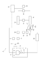
図1に示されるように、半導体デバイス検査装置1は、被検査デバイス(DUT:Device Under Test)である半導体デバイス8において異常発生箇所を特定するなど、半導体デバイス8を検査するための装置である。半導体デバイス8としては、トランジスタ等のPNジャンクションを有する集積回路(例えば、小規模集積回路(SSI:Small Scale Integration)、中規模集積回路(MSI:Medium Scale Integration)、大規模集積回路(LSI:Large Scale Integration)、超大規模集積回路(VLSI:Very Large Scale Integration)、超々大規模集積回路(ULSI:Ultra Large Scale Integration)、ギガ・スケール集積回路(GSI:Giga Scale Integration))、大電流用/高圧用MOSトランジスタ及びバイポーラトランジスタ等がある。また、半導体デバイス8は、熱による変調を基板にかけられる半導体デバイスであってもよい。 As shown in FIG. 1, a semiconductor device inspection apparatus 1 is an apparatus for inspecting a semiconductor device 8 such as specifying an abnormality occurrence location in a semiconductor device 8 that is a device under test (DUT). . The semiconductor device 8 includes an integrated circuit having a PN junction such as a transistor (for example, a small scale integrated circuit (SSI), a medium scale integrated circuit (MSI), a large scale integrated circuit (LSI: Large). Scale Integration), Very Large Scale Integration (VLSI), Ultra Large Scale Integration (ULSI), Giga Scale Integration (GSI)), High Current / High Voltage There are MOS transistors and bipolar transistors. The semiconductor device 8 may be a semiconductor device that can be modulated by heat on the substrate.
半導体デバイス検査装置1は、レーザ光源(光発生部)2を備えている。レーザ光源2は、第1電源(図示せず)によって動作させられ、半導体デバイス8に照射される光を出射する。レーザ光源2から出射された光は、プローブ光用の偏光保存シングルモード光ファイバ3を介して、スキャン光学系5に導光される。スキャン光学系5は、スキャンヘッド6及びレンズ系7を有している。これにより、スキャン光学系5に導光された光は、半導体デバイス8の所定位置に結像され、当該光の照射領域は、半導体デバイス8に対して2次元的に走査される。なお、スキャン光学系5及び半導体デバイス8は、暗箱4内に配置されている。 The semiconductor device inspection apparatus 1 includes a laser light source (light generation unit) 2. The laser light source 2 is operated by a first power source (not shown), and emits light irradiated on the semiconductor device 8. The light emitted from the laser light source 2 is guided to the scanning optical system 5 through the polarization-preserving single mode optical fiber 3 for probe light. The scan optical system 5 has a scan head 6 and a lens system 7. Thereby, the light guided to the scanning optical system 5 forms an image at a predetermined position of the semiconductor device 8, and the irradiation region of the light is scanned two-dimensionally with respect to the semiconductor device 8. The scanning optical system 5 and the semiconductor device 8 are disposed in the dark box 4.
レーザ光源2から出射された光が半導体デバイス8に照射されたときに半導体デバイス8で反射された反射光は、戻り光用の光ファイバ9を介して、光センサ(光検出部)10に導光される。光センサ10は、第1電源(図示せず)と別体で設けられた第2電源(図示せず)によって動作させられ、反射光を検出して検出信号を出力する。光センサ10から出力された検出信号は、アンプ11を介して、分岐回路12に入力される。分岐回路12は検出信号を分岐して出力する。分岐された検出信号の一方はスペクトラムアナライザ(第1の電気計測部/第1のスペクトル分析部/第1のスペクトラムアナライザ)13に入力され、分岐された検出信号の他方は、アテネ―タ18、アンプ19、及び切替部17を介してスペクトラムアナライザ(第2の電気計測部/第2のスペクトル分析部/第2のスペクトラムアナライザ)14に入力される。なお、スペクトル分析部は、スペクトラムアナライザなどの複合波の信号の各成分の振幅を測定する電気計測手段である。
The reflected light reflected by the semiconductor device 8 when the light emitted from the laser light source 2 is applied to the semiconductor device 8 is guided to the optical sensor (light detection unit) 10 through the
スペクトラムアナライザ13,14は、信号同期部15を介して互いに電気的に接続されている。また、スペクトラムアナライザ13,14は、出力信号処理部16と電気的に接続されている。スペクトラムアナライザ13,14は、入力された電気信号(詳細は後述)に基づき信号を生成し、該信号を出力信号処理部16に入力する。出力信号処理部16は、スペクトラムアナライザ13,14により入力された信号に基づいて解析信号を生成し、該解析信号に基づく半導体デバイス像を形成し、当該半導体デバイス像を表示部20に表示させる。
The
出力信号処理部16には、レーザスキャンコントローラ21が電気的に接続されている。レーザスキャンコントローラ21は、レーザ光源2及びスキャン光学系5を制御する。スペクトラムアナライザ13,14には、テスタ、パルスジェネレータ及び電源を含むテスタユニット(駆動信号印加部)22が電気的に接続されている。テスタユニット22は、所定の変調周波数を有する駆動信号(テストパターン)を半導体デバイス8に印加する。これにより、半導体デバイス8は、検査時に駆動させられる。
A
次に、切替部17、アテネ―タ18、アンプ19について、より詳細に説明する。切替部17は、スペクトラムアナライザ14に入力される信号を切り替える機能を有する。切替部17は、光センサ10と電気的に接続された検出信号端子(第1の信号端子)17aと、テスタユニット22と電気的に接続された駆動信号端子(第2の信号端子)17bと、一端17dがスペクトラムアナライザ14と電気的に接続された接続部17cと、を有している。切替部17によるスペクトラムアナライザ14に入力される信号の切り替えは、接続部17cの他端17eを検出信号端子17a又は駆動信号端子17bのいずれかに接続することにより行われる。すなわち、他端17eが検出信号端子17aに接続されている場合にはスペクトラムアナライザ14には分岐回路12により分岐された検出信号が入力され、他端17eが駆動信号端子17bに接続されている場合にはスペクトラムアナライザ14にはテスタユニット22から出力された駆動信号が入力される。なお、分岐回路12にアンプ19を接続し、切替部17の検出信号端子17aにアテネータ18を接続しても良い。
Next, the switching
アテネ―タ18及びアンプ19は、スペクトラムアナライザ13と検出信号端子17aとの間に設けられている。アテネ―タ18は、信号減衰部としての機能を有している。アテネ―タ18は、光センサ10から検出信号端子17aへ向かって流れる検出信号、検出信号端子17aからスペクトラムアナライザ13へ向かって逆流する反射信号、及び、検出信号端子17aからスペクトラムアナライザ13へ向かって流れるクロストーク信号、の各電気信号を減衰する。ここで、検出信号端子17aからスペクトラムアナライザ13に向かって逆流する反射信号とは、切替部17の他端17eが駆動信号端子17bに接続されている際に、分岐回路12から検出信号端子17aに向かって流れていた検出信号のうち、例えば、切替部17の検出信号端子17aで反射しスペクトラムアナライザ13に向かって逆流する信号をいう。また、検出信号端子17aからスペクトラムアナライザ13に向かって流れるクロストーク信号とは、切替部17の他端17eが駆動信号端子17bに接続されている状態において、駆動信号端子17bからスペクトラムアナライザ14に向かって流れる駆動信号が、接続されていない検出信号端子17a(もしくは配線)に、電気的作用によって漏れる(まわり込む)ことによって発生するスペクトラムアナライザ13に向かって流れる信号をいう。
The
アンプ19は、光検出部10から検出信号端子17aへ向かって流れる電気信号を所定の増幅率で増幅し、また、検出信号端子17aからスペクトラムアナライザ13へ向かって流れる電気信号を減衰する。したがって、アンプ19は、信号増幅部としての機能と信号減衰部としての機能を両方とも有している。これにより、アンプ19は、光センサ10からアテネ―タ18を介して検出信号端子17aに向かって流れる検出信号を増幅するように設定されている。すなわち、光センサ10から出力された検出信号は、アテネ―タ18で一度減衰された後、アンプ19によって減衰前の強度と同等になるように増幅される。また、アンプ19は、検出信号端子17aからスペクトラムアナライザ13に向かって流れる反射信号及びクロストーク信号については、増幅せず、減衰させるように設定されている。このようなアンプ19としては、アイソレーションアンプやバッファアンプなどを用いることができる。また、アンプ19は、信号の増幅率を切り替える構成としても良い。この場合、アンプ19の増幅率を制御するアンプ制御部(不図示)をさらに備え、アンプ制御部(不図示)によって、入力された信号に対する増幅率を切り替える。これにより、アンプ19は、光検出部10から検出信号端子17aに向かって流れる電気信号を所定の増幅率で増幅し、また、検出信号端子17aからスペクトラムアナライザ13へ向かって流れる電気信号を、増幅しない、もしくは、低い増幅率で増幅する。
The
次に、スペクトラムアナライザ13,14、信号同期部15、出力信号処理部16について、より詳細に説明する。スペクトラムアナライザ13には検出信号が入力される。また、スペクトラムアナライザ14には検出信号及び駆動信号が選択的に入力される。具体的に、他端17eが検出信号端子17aに接続されている場合には、スペクトラムアナライザ13,14には、光センサ10で検出された検出信号が入力される。この場合、出力信号処理部16は、スペクトラムアナライザ13に入力された検出信号に対して測定周波数帯域FR1を,スペクトラムアナライザ14に入力された検出信号に対して測定周波数帯域FR2を、それぞれ設定する。スペクトラムアナライザ13は測定周波数帯域FR1における検出信号から生成した信号を出力信号処理部16に入力する。また、スペクトラムアナライザ14は測定周波数帯域FR2における検出信号から生成した信号を出力信号処理部16に入力する。そして、出力信号処理部16は、スペクトラムアナライザ13,14から入力された信号の差分を算出することにより、解析信号を取得する。
Next, the
また、切替部17の他端17eが駆動信号端子17bに接続されている場合には、スペクトラムアナライザ13には光センサ10で検出された検出信号が入力され、スペクトラムアナライザ14にはテスタユニット22により半導体デバイス8に印加される駆動信号もしくは駆動信号の繰り返し周波数の整数倍の信号がリファレンス信号として入力される。スペクトラムアナライザ13は検出信号から所定の周波数の信号を抽出し出力信号処理部16に入力する。スペクトラムアナライザ14はリファレンス信号の周波数の信号を抽出し出力信号処理部16に入力する。そして、出力信号処理部16は、スペクトラムアナライザ13により入力された信号と、スペクトラムアナライザ14により入力された信号との位相差を算出し、該位相差に基づいた位相画像を作成する。このような位相差を算出する前提として、信号同期部15により、スペクトラムアナライザ13を動作させる基準信号の周波数及び位相と、スペクトラムアナライザ14を動作させる基準信号の周波数及び位相とが同期するように制御される。
When the
次に、半導体デバイス検査装置1を用いた2つの計測手法(第1及び第2の計測手法)について説明する。第1の計測手法は、検出信号端子17aに他端17eを接続して異常周波数を特定した後に、駆動信号端子17bに他端17eを接続し故障個所及び故障原因を特定する手法である。
Next, two measurement methods (first and second measurement methods) using the semiconductor device inspection apparatus 1 will be described. The first measurement method is a method in which after the
第1の計測手法では、まず、切替部17の他端17eを検出信号端子17aに接続する。このとき、スペクトラムアナライザ13,14には、それぞれ光センサ10において検出された検出信号が入力される。なお、スペクトラムアナライザ13,14それぞれに入力される検出信号は、複数の周波数の信号からなる。そして、出力信号処理部16に対して、スペクトラムアナライザ13が測定周波数帯域FR1の信号を抽出し出力するように、スペクトラムアナライザ14が測定周波数帯域FR2の信号を抽出し出力するように、それぞれ設定する。なお、測定周波数帯域FR1と測定周波数帯域FR2とは異なる周波数帯域である。
In the first measurement method, first, the
上述した、出力信号処理部16の設定について説明する。例えば、テスタユニット22が、第1変調周波数を有する第1駆動信号、及び第1変調周波数と異なる第2変調周波数を有する第2駆動信号を半導体デバイス8に印加する場合において、それらの信号による変調を同時に観察するために、出力信号処理部16は、第1駆動信号の第1変調周波数及び第2駆動信号の第2変調周波数に基づいて、測定周波数帯域FR1及び測定周波数帯域FR2を設定する。すなわち、測定周波数帯域FR1は、第1駆動信号の第1変調周波数のN倍(Nは自然数)の周波数を含むように設定され、測定周波数帯域FR2は、第2駆動信号の第2変調周波数のN倍(Nは自然数)の周波数を含むように設定される。これによれば、図2に示されるように、スペクトラムアナライザ13で生成された測定周波数帯域FR1に基づく測定信号S1と、スペクトラムアナライザ14で生成された測定周波数帯域FR2に基づく測定信号S2との差分から、測定周波数帯域FR1,FR2において、それぞれ、半導体デバイス検査装置のもつ固有の雑音等が除去された解析信号が取得できる。当該解析信号は、出力信号処理部16によって、表示部20に振幅像が表示される。
The setting of the output
そして、表示部20に表示された解析信号の振幅像を確認し、通常の振幅像と異なる像となっている周波数を、故障に起因する信号を含む周波数(異常周波数)として特定する。なお、解析信号の振幅像確認は、異常周波数が取得されるまで、測定周波数帯域FR1,FR2の設定を変更し繰り返し行われる。
Then, the amplitude image of the analysis signal displayed on the
そして、異常周波数が特定された場合には、切替部17の他端17eを、検出信号端子17aに接続された状態から駆動信号端子17bに接続された状態に切り替える。このとき、スペクトラムアナライザ13には光センサ10において検出された検出信号が、スペクトラムアナライザ14にはテスタユニット22により半導体デバイス8に印加される駆動信号が、それぞれ入力される。スペクトラムアナライザ13には、上述した異常周波数の検出信号が入力される。なお、信号同期部15の設定により、スペクトラムアナライザ13を動作させる基準信号の周波数及び位相と、スペクトラムアナライザ14を動作させる基準信号の周波数及び位相とを同期するように制御する。
When the abnormal frequency is specified, the
スペクトラムアナライザ13,14から出力された信号は、出力信号処理部16に入力される。そして、出力信号処理部16により、スペクトラムアナライザ13,14から出力された信号の位相差が算出され、該位相差に基づく位相画像が表示部20に表示される。このような位相画像は、スキャン光学系5に導光される半導体デバイス8における光の照射領域を変更し、各照射領域について作成される。位相画像は、位相差に基づいた色で表示される。照射領域毎のスペクトラムアナライザ13,14から出力される信号の位相差として適正な色を把握しておくことで、該適正な色と乖離した色となっている(あるべき位相差となっていない)箇所を、半導体デバイス8の故障個所として特定できる。また、適正な色との乖離度合や、特定の色であるか否かなどによって、故障原因を特定できる。なお、故障原因とは、例えば半導体デバイス8の素子間の配線が切れている、高抵抗の部分がある、などである。
The signals output from the
つづいて、第2の計測手法について説明する。第2の計測手法は、駆動信号端子17bに他端17eを接続して位相差から故障個所及び故障原因を特定した後に、検出信号端子17aに他端17eを接続し半導体デバイス検査装置のもつ固有の雑音が除去された信号を取得する手法である。
Next, the second measurement method will be described. In the second measurement method, the
第2の計測手法では、まず、切替部17の他端17eを駆動信号端子17bに接続する。このとき、スペクトラムアナライザ13には光センサ10において検出された検出信号が、スペクトラムアナライザ14にはテスタユニット22により半導体デバイス8に印加される駆動信号が、それぞれ入力される。出力信号処理部16に対しては、スペクトラムアナライザ13が検出信号の中から所定の周波数の信号を抽出し出力するように設定し、スペクトラムアナライザ14が駆動信号の周波数の信号を抽出し出力するように設定する。
In the second measurement method, first, the
スペクトラムアナライザ13,14から出力された信号は、出力信号処理部16に入力される。そして、出力信号処理部16により、スペクトラムアナライザ13,14から出力された信号の位相差が算出され、該位相差に基づく位相画像が表示部20に表示される。このような位相画像は、スキャン光学系5に導光される半導体デバイス8における光の照射領域を変更し、各照射領域について作成される。位相画像は、位相差に基づいた色で表示される。位相画像から故障個所を特定すると、該故障個所が光の照射領域となるようにスキャン光学系5を調整する。
The signals output from the
そして、切替部17の他端17eを、駆動信号端子17bに接続された状態から検出信号端子17aに接続された状態に切り替える。このとき、スペクトラムアナライザ13,14には、それぞれ光センサ10において検出された検出信号が入力される。なお、光センサ10からの信号は、複数の周波数の信号からなる。そして、出力信号処理部16に対して、図3に示すように、スペクトラムアナライザ13が所定の周波数帯域(測定用周波数帯域)FR1の信号を抽出し出力するように設定し、スペクトラムアナライザ14が半導体デバイス検査装置のもつ固有の雑音のうち周波数依存のない周波数帯域を加算したレベル以下となる周波数帯域(参照用周波数帯域)FR2の信号を抽出し出力するように設定する。
Then, the
そして、出力信号処理部16がスペクトラムアナライザ13及びスペクトラムアナライザ14から入力された信号の差分をとることで、ホワイトノイズが除去された信号(解析信号)を取得することができる。解析信号を用いることで、計測結果の高精度化が図られる。
The output
以上説明したように、半導体デバイス検査装置1では、半導体デバイス8に照射される光を発生する光発生工程と、光発生工程において発生した光が半導体デバイス8に照射されたときに半導体デバイス8で反射された反射光を検出し検出信号を出力する光検出工程と、半導体デバイス8を駆動させる駆動信号を半導体デバイス8に印加する駆動信号印加工程と、検出信号をスペクトラムアナライザ13に入力する第1の測定工程と、検出信号及び駆動信号をスペクトラムアナライザ14に選択的に入力する第2の測定工程と、を含む半導体デバイス検査方法が実施される。
As described above, in the semiconductor device inspection apparatus 1, the light generation process for generating the light applied to the semiconductor device 8 and the semiconductor device 8 when the light generated in the light generation process is applied to the semiconductor device 8. A light detection step of detecting reflected reflected light and outputting a detection signal, a drive signal applying step of applying a drive signal for driving the semiconductor device 8 to the semiconductor device 8, and a first of inputting the detection signal to the
また、第2の測定工程は、上述したように、検出信号をスペクトラムアナライザ14に入力した後に駆動信号をスペクトラムアナライザ14に入力する手法と、駆動信号をスペクトラムアナライザ14に入力した後に検出信号をスペクトラムアナライザ14に入力する手法とがある。
In addition, as described above, the second measurement step includes a method of inputting the detection signal to the
このように、半導体デバイス検査装置1では、切替部17が他端17eの接続先を検出信号端子17aとした場合には、スペクトラムアナライザ13,14で2つの周波数の振幅同時計測が可能である。すなわち、半導体デバイス8の検査を効率的に行える。また、切替部17が他端17eの接続先を駆動信号端子17bとして場合には、スペクトラムアナライザ13には検出信号が入力されスペクトラムアナライザ14には駆動信号が入力されることとなるため、検出信号の位相と駆動信号の位相とから位相差が算出でき、該位相差より故障個所及び故障原因を特定できる。すなわち、半導体デバイス8の検査を精度良く行うことができる。以上より、この半導体デバイス検査装置1によれば、半導体デバイス8の検査を効率良く且つ精度良く実施することができる。
As described above, in the semiconductor device inspection apparatus 1, when the switching
また、切替部17が他端17eを駆動信号端子17bに接続する場合に、スペクトラムアナライザ13を動作させる基準信号の周波数及び位相と、スペクトラムアナライザ14を動作させる基準信号の周波数及び位相とを同期させる信号同期部15を備えることで、各スペクトラムアナライザ13,14間の基準周波数の誤差に起因する位相差が重畳されることが防止されるため、検出信号と駆動信号との位相差をより精度良く算出できる。
Further, when the switching
また、スペクトラムアナライザ13と検出信号端子との間に設けられ、切替部17が検出信号端子に接続していた他端17eを駆動信号端子17bに接続する場合に、検出信号端子からスペクトラムアナライザ13へ向かう方向に流れる電気信号を減衰する信号減衰部を更に備えることで、切替部17が他端17eの接続を検出信号端子17aから駆動信号端子17bに切り替えた際に、検出信号端子17aからスペクトラムアナライザ13に向かって逆流する検出信号、及び、検出信号端子17aからスペクトラムアナライザ13に向かって流れる駆動信号を適切に減衰できる。これにより、ノイズ信号がスペクトラムアナライザ13に入力されることを防止でき、検出信号と駆動信号との位相差をより精度良く算出できる。
Further, when the
以上、本発明の一実施形態について説明したが、本発明は上記実施形態に限定されるものではない。例えば、半導体デバイス8に照射される光を発生する光発生部は、レーザ光源2に限定されず、スーパールミネッセントダイオード等の他の光源であってもよい。また、半導体デバイス8に対し、電気信号に代えて、熱を印加してもよい。また、第1の電気計測部および第2の電気計測部としては、スペクラムアナライザなどのスペクトル分析器に限らず、ロックインアンプやオシロスコープなどさまざまな電気計測機器(またはそれらの機能を有する装置)でもよい。また、それらの電気計測機器を組み合わせてもよく、例えば、第1の電気計測部としてスペクトラムアナライザを、第2の電気計測部としてロックインアンプを採用してもよい。さらに、複数のスペクトル分析部を備えるスペクトラムアナライザを用いても良い。このようなスペクトラムアナライザは、スペクトラムアナライザ13に相当する第1の電気計測部に信号を入力する第1のチャンネルとスペクトラムアナライザ14に相当する第2の電気計測部に信号を入力する第2のチャンネルを備えており、第1のチャンネルは、分岐回路12に電気的に接続され、第2のチャンネルは切替部17の他端17dに電気的に接続される。
Although one embodiment of the present invention has been described above, the present invention is not limited to the above embodiment. For example, the light generation unit that generates the light applied to the semiconductor device 8 is not limited to the laser light source 2 but may be another light source such as a super luminescent diode. Further, heat may be applied to the semiconductor device 8 instead of the electrical signal. Further, the first electric measurement unit and the second electric measurement unit are not limited to spectrum analyzers such as a spectrum analyzer, but various electric measurement devices such as lock-in amplifiers and oscilloscopes (or devices having these functions). But you can. Moreover, you may combine those electrical measuring devices, for example, you may employ | adopt a spectrum analyzer as a 1st electrical measurement part, and a lock-in amplifier as a 2nd electrical measurement part. Further, a spectrum analyzer including a plurality of spectrum analysis units may be used. Such a spectrum analyzer has a first channel for inputting a signal to a first electric measurement unit corresponding to the
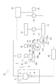
また、図4に示される半導体デバイス検査装置1xのように、信号減衰部として、グランド端子23bに接続された電気抵抗23aを有する信号減衰機構23を備えるとともに、一端が該電気抵抗23aと接続された減衰切替部17fを備え、切替部17が検出信号端子17aに接続していた他端17eを駆動信号端子17bに接続する場合に、減衰切替部17fの電気抵抗23aと接続されていない側の端部が検出信号端子17aに接続される構成であってもよい。この構成によれば、切替部17が他端17eの接続を検出信号端子17aから駆動信号端子17bに切り替えた場合に、減衰切替部17fが検出信号端子17aに接続されるため、検出信号端子17aからスペクトラムアナライザ13に向かって流れる電気信号はグランドに出力されることとなる。よって、検出信号端子17aからスペクトラムアナライザ13に向かって流れる電気信号を適切に減衰できる。なお、検出信号端子17aと分岐回路12との間にアテネータ18とアンプ19から構成される信号減衰部を更に備えても良い。
Further, as in the semiconductor
また、図5に示される半導体デバイス検査装置1yのように、信号減衰部として、グランド端子25bに接続された電気抵抗25aを有する信号減衰機構25を備えるとともに、分岐回路12と電気的に接続された分岐回路端子(第4の信号端子)24aと、電気抵抗25aと電気的に接続された減衰端子(第3の信号端子)24bと、一端が検出信号端子17aと電気的に接続され他端と、分岐回路端子24aが減衰端子24b又は一端が検出信号端子17aと電気的に接続され他端のいずれかと電気的に接続可能とされた中間接続部24cと、から構成された中間切替部24を有してもよい。この構成によれば、切替部17が他端17eを検出信号端子17aに接続している場合には中間接続部24cを一端が検出信号端子17aと電気的に接続され他端に接続し、切替部17が他端17eの接続を検出信号端子17aから駆動信号端子17bに切り替えた場合には中間接続部24cを減衰端子24bに接続することで、分岐回路端子24aからスペクトラムアナライザ13に向かって流れる電気信号はグランドに出力されることとなる。よって、検出信号端子17aからスペクトラムアナライザ13に向かって流れる電気信号を適切に減衰できる。なお、分岐回路端子24aと分岐回路12との間にアテネータ18とアンプ19から構成される信号減衰部を更に備えても良い。
Further, as in the semiconductor
1,1x,1y…半導体デバイス検査装置、2…レーザ光源(光発生部)、8…半導体デバイス、10…光センサ(光検出部)、12…分岐回路、13…スペクトラムアナライザ(第1の電気計測部、第1のスペクトル分析部、第1のスペクトラムアナライザ)、14…スペクトラムアナライザ(第2の電気計測部、第2のスペクトル分析部、第2のスペクトラムアナライザ)、15…信号同期部、16…出力信号処理部、17…切替部、17a…検出信号端子(第1の信号端子)、17b…駆動信号端子(第2の信号端子)、17c…接続部、17d…一端、17e…他端、17f…減衰切替部、18…アテネ―タ(信号減衰部/減衰器)、19…アンプ(信号減衰部/増幅器)、20…表示部、22…テスタユニット(駆動信号印加部)、23a,25a…電気抵抗、23b,25b…グランド、24a…分岐回路端子(第4の信号端子)、24b…減衰端子(第3の信号端子)、24c…中間接続部。
DESCRIPTION OF
Claims (12)
前記光発生部が発生した前記光が前記半導体デバイスに照射されたときに前記半導体デバイスで反射された反射光を検出し、検出信号を出力する光検出部と、
前記半導体デバイスを駆動させる駆動信号を前記半導体デバイスに印加する駆動信号印加部と、
前記検出信号が入力される第1の電気計測部と、
前記検出信号及び前記駆動信号が選択的に入力される第2の電気計測部と、
前記光検出部と電気的に接続された第1の信号端子、前記駆動信号印加部と電気的に接続された第2の信号端子、及び、一端が前記第2の電気計測部と電気的に接続された接続部を有する切替部と、を備え、
前記切替部は、前記接続部の他端を前記第1の信号端子に接続することで前記第2の電気計測部に前記検出信号を入力させ、前記接続部の前記他端を前記第2の信号端子に接続することで前記第2の電気計測部に前記駆動信号を入力させる、半導体デバイス検査装置。A light generating section for generating light irradiated to a semiconductor device which is a device to be inspected;
A light detection unit that detects reflected light reflected by the semiconductor device when the light generated by the light generation unit is applied to the semiconductor device, and outputs a detection signal;
A drive signal applying unit for applying a drive signal for driving the semiconductor device to the semiconductor device;
A first electrical measurement unit to which the detection signal is input;
A second electrical measurement unit to which the detection signal and the drive signal are selectively input;
A first signal terminal electrically connected to the light detection unit; a second signal terminal electrically connected to the drive signal application unit; and one end electrically connected to the second electric measurement unit. A switching unit having a connected connection part,
The switching unit causes the second electric measurement unit to input the detection signal by connecting the other end of the connection unit to the first signal terminal, and connects the other end of the connection unit to the second signal terminal. A semiconductor device inspection apparatus that inputs the drive signal to the second electrical measurement unit by connecting to a signal terminal.
前記切替部は、前記電気抵抗と電気的に接続された減衰切替部を有し、
前記切替部は、前記接続部の前記他端を前記第2の信号端子に接続する場合に、前記減衰切替部を前記第1の信号端子に電気的に接続する、請求項2記載の半導体デバイス検査装置。The signal attenuating unit has an electrical resistance electrically connected to the ground,
The switching unit has an attenuation switching unit electrically connected to the electrical resistance,
The semiconductor device according to claim 2, wherein the switching unit electrically connects the attenuation switching unit to the first signal terminal when the other end of the connection unit is connected to the second signal terminal. Inspection device.
前記切替部は、前記電気抵抗と電気的に接続された第3の信号端子、前記光検出部と電気的に接続された第4の信号端子、及び、一端が前記第1の信号端子と電気的に接続された中間接続部を更に有し、
前記切替部は、前記接続部の前記他端を前記第1の信号端子に接続する場合に、前記中間接続部を前記第4の信号端子に接続し、前記接続部の前記他端を前記第2の信号端子に接続する場合に、前記中間接続部を前記第3の信号端子に接続する、請求項2記載の半導体デバイス検査装置。The signal attenuating unit has an electrical resistance electrically connected to the ground,
The switching unit includes a third signal terminal electrically connected to the electrical resistance, a fourth signal terminal electrically connected to the light detection unit, and one end electrically connected to the first signal terminal. And further having an intermediate connection connected
The switching unit connects the intermediate connection unit to the fourth signal terminal and connects the other end of the connection unit to the first signal terminal when the other end of the connection unit is connected to the first signal terminal. 3. The semiconductor device inspection apparatus according to claim 2, wherein when connecting to the second signal terminal, the intermediate connection portion is connected to the third signal terminal.
前記光発生工程において発生した前記光が前記半導体デバイスに照射されたときに、前記半導体デバイスで反射された反射光を検出し、検出信号を出力する光検出工程と、
前記半導体デバイスを駆動させる駆動信号を前記半導体デバイスに印加する駆動信号印加工程と、
前記検出信号を第1の電気計測部に入力する第1の測定工程と、
前記検出信号及び前記駆動信号を第2の電気計測部に選択的に入力する第2の測定工程と、を含む、半導体デバイス検査方法。A light generation step for generating light irradiated on a semiconductor device as a device to be inspected;
A light detection step of detecting reflected light reflected by the semiconductor device and outputting a detection signal when the light generated in the light generation step is irradiated on the semiconductor device;
A drive signal applying step of applying a drive signal for driving the semiconductor device to the semiconductor device;
A first measurement step of inputting the detection signal to a first electrical measurement unit;
And a second measurement step of selectively inputting the detection signal and the drive signal to a second electric measurement unit.
Priority Applications (1)
| Application Number | Priority Date | Filing Date | Title |
|---|---|---|---|
| JP2014559747A JP5744353B2 (en) | 2013-02-01 | 2014-01-30 | Semiconductor device inspection apparatus and semiconductor device inspection method |
Applications Claiming Priority (4)
| Application Number | Priority Date | Filing Date | Title |
|---|---|---|---|
| JP2013018683 | 2013-02-01 | ||
| JP2013018683 | 2013-02-01 | ||
| JP2014559747A JP5744353B2 (en) | 2013-02-01 | 2014-01-30 | Semiconductor device inspection apparatus and semiconductor device inspection method |
| PCT/JP2014/052145 WO2014119675A1 (en) | 2013-02-01 | 2014-01-30 | Semiconductor device inspection device and semiconductor device inspection method |
Publications (2)
| Publication Number | Publication Date |
|---|---|
| JP5744353B2 true JP5744353B2 (en) | 2015-07-08 |
| JPWO2014119675A1 JPWO2014119675A1 (en) | 2017-01-26 |
Family
ID=51262384
Family Applications (3)
| Application Number | Title | Priority Date | Filing Date |
|---|---|---|---|
| JP2014559748A Active JP5745707B2 (en) | 2013-02-01 | 2014-01-30 | Semiconductor device inspection apparatus and semiconductor device inspection method |
| JP2014559747A Active JP5744353B2 (en) | 2013-02-01 | 2014-01-30 | Semiconductor device inspection apparatus and semiconductor device inspection method |
| JP2015094299A Active JP6389797B2 (en) | 2013-02-01 | 2015-05-01 | Semiconductor device inspection apparatus and semiconductor device inspection method |
Family Applications Before (1)
| Application Number | Title | Priority Date | Filing Date |
|---|---|---|---|
| JP2014559748A Active JP5745707B2 (en) | 2013-02-01 | 2014-01-30 | Semiconductor device inspection apparatus and semiconductor device inspection method |
Family Applications After (1)
| Application Number | Title | Priority Date | Filing Date |
|---|---|---|---|
| JP2015094299A Active JP6389797B2 (en) | 2013-02-01 | 2015-05-01 | Semiconductor device inspection apparatus and semiconductor device inspection method |
Country Status (5)
| Country | Link |
|---|---|
| US (4) | US9562944B2 (en) |
| JP (3) | JP5745707B2 (en) |
| KR (5) | KR20170069292A (en) |
| SG (3) | SG11201505836WA (en) |
| WO (2) | WO2014119676A1 (en) |
Families Citing this family (12)
| Publication number | Priority date | Publication date | Assignee | Title |
|---|---|---|---|---|
| WO2014119676A1 (en) | 2013-02-01 | 2014-08-07 | 浜松ホトニクス株式会社 | Semiconductor device inspection device and semiconductor device inspection method |
| JP2016109673A (en) * | 2014-10-16 | 2016-06-20 | ディーシージー システムズ、 インコーポレイテッドDcg Systems Inc. | Systems and method for laser voltage imaging |
| JP6714485B2 (en) * | 2016-09-28 | 2020-06-24 | 浜松ホトニクス株式会社 | Semiconductor device inspection method and semiconductor device inspection apparatus |
| JP2018072290A (en) * | 2016-11-04 | 2018-05-10 | ルネサスエレクトロニクス株式会社 | Fault location specification device and fault location specification method |
| JP7159312B2 (en) * | 2018-06-28 | 2022-10-24 | 株式会社日立ハイテク | Semiconductor inspection equipment |
| US11011435B2 (en) * | 2018-11-20 | 2021-05-18 | Asm Technology Singapore Pte Ltd | Apparatus and method inspecting bonded semiconductor dice |
| JP7164488B2 (en) * | 2019-05-31 | 2022-11-01 | 浜松ホトニクス株式会社 | Semiconductor device inspection method and semiconductor device inspection apparatus |
| US11133864B1 (en) * | 2020-04-24 | 2021-09-28 | Ciena Corporation | Measurement of crosstalk |
| KR102425048B1 (en) * | 2020-12-24 | 2022-07-27 | 큐알티 주식회사 | Inspection apparatus of beam for testing of semiconductor, and method of inspection for beam |
| KR102586199B1 (en) * | 2021-10-21 | 2023-10-06 | 큐알티 주식회사 | Test method of power semiconductor device, and test system for the same |
| KR102418633B1 (en) * | 2021-12-22 | 2022-07-07 | 큐알티 주식회사 | A semiconductor device radiation test method, and a semiconductor device radiation test system |
| KR102518783B1 (en) * | 2022-06-23 | 2023-04-06 | 큐알티 주식회사 | Beam controller capable of adaptive deformation, a test apparatus for semiconductor device using the same, and a test method for semiconductor device using the same |
Family Cites Families (34)
| Publication number | Priority date | Publication date | Assignee | Title |
|---|---|---|---|---|
| JPH01169862A (en) | 1987-12-25 | 1989-07-05 | Hitachi Ltd | Charged particle beam device |
| JPH0513522A (en) * | 1991-07-04 | 1993-01-22 | Advantest Corp | Charged optical probe |
| JPH0547883A (en) | 1991-08-12 | 1993-02-26 | Nippon Telegr & Teleph Corp <Ntt> | Method and apparatus for testing integrated circuit |
| JP3154531B2 (en) * | 1991-12-18 | 2001-04-09 | 富士通株式会社 | Signal measurement device |
| JPH06201803A (en) | 1992-12-28 | 1994-07-22 | Fujitsu Ltd | Apparatus and method for measuring signal waveform |
| JPH07134147A (en) * | 1993-11-10 | 1995-05-23 | Fujitsu Ltd | Signal waveform measuring device |
| SE502886C2 (en) | 1994-06-13 | 1996-02-12 | Whirlpool Europ | Control method for a microwave oven, microwave oven and its use for cooking / heating a food product according to the control procedure |
| GB9411908D0 (en) | 1994-06-14 | 1994-08-03 | John Heyer Paper Ltd | Web monitoring for paper machines |
| JP3500215B2 (en) * | 1995-02-07 | 2004-02-23 | 浜松ホトニクス株式会社 | Voltage measuring device |
| JP3500216B2 (en) | 1995-02-07 | 2004-02-23 | 浜松ホトニクス株式会社 | Voltage measuring device |
| DE19511869B4 (en) | 1995-03-31 | 2004-02-26 | Geiler, Hans-Dieter, Dr. | Method and arrangement for response analysis of semiconductor materials with optical excitation |
| KR960035045U (en) | 1995-04-13 | 1996-11-21 | 김헌영 | Packing material used for finishing pipe insulation |
| US5905577A (en) | 1997-03-15 | 1999-05-18 | Schlumberger Technologies, Inc. | Dual-laser voltage probing of IC's |
| JPH11271363A (en) | 1998-03-19 | 1999-10-08 | Ando Electric Co Ltd | Electro-optic sampling oscilloscope |
| US6252222B1 (en) | 2000-01-13 | 2001-06-26 | Schlumberger Technologies, Inc. | Differential pulsed laser beam probing of integrated circuits |
| US6976234B2 (en) * | 2003-01-13 | 2005-12-13 | Credence Systems Corporation | Apparatus and method for measuring characteristics of dynamic electrical signals in integrated circuits |
| JP2005134196A (en) | 2003-10-29 | 2005-05-26 | Nec Electronics Corp | Non-destructive analysis method and non-destructive analysis device |
| KR100674972B1 (en) | 2005-05-24 | 2007-01-29 | 삼성전자주식회사 | System and method of measuring pulse properties of semiconductor device |
| US7659981B2 (en) | 2005-08-26 | 2010-02-09 | Dcg Systems, Inc. | Apparatus and method for probing integrated circuits using polarization difference probing |
| US7733100B2 (en) * | 2005-08-26 | 2010-06-08 | Dcg Systems, Inc. | System and method for modulation mapping |
| JP5340524B2 (en) | 2006-03-23 | 2013-11-13 | 浜松ホトニクス株式会社 | Radiation detector and radiation detection method |
| US7999949B2 (en) * | 2006-04-24 | 2011-08-16 | Raintree Scientific Instruments (Shanghai) Corporation | Spectroscopic ellipsometers |
| JP5181989B2 (en) | 2008-10-03 | 2013-04-10 | ソニー株式会社 | Short pulse light source device, laser driving method, optical pickup and optical disk device |
| SG10201401887YA (en) * | 2009-05-01 | 2014-06-27 | Dcg Systems Inc | Systems and method for laser voltage imaging state mapping |
| JP2011075441A (en) * | 2009-09-30 | 2011-04-14 | Hamamatsu Photonics Kk | Semiconductor device failure analysis apparatus |
| US8309883B2 (en) | 2010-05-20 | 2012-11-13 | Ipg Photonics Corporation | Methods and systems for laser processing of materials |
| US8564301B2 (en) | 2010-11-08 | 2013-10-22 | Semiconductor Components Industries, Llc | Device and method for determining capacitance as a function of voltage |
| JP5894745B2 (en) | 2011-05-31 | 2016-03-30 | 浜松ホトニクス株式会社 | Integrated circuit inspection equipment |
| JP6166032B2 (en) | 2012-11-06 | 2017-07-19 | 浜松ホトニクス株式会社 | Semiconductor device inspection apparatus and semiconductor device inspection method |
| WO2014119676A1 (en) | 2013-02-01 | 2014-08-07 | 浜松ホトニクス株式会社 | Semiconductor device inspection device and semiconductor device inspection method |
| JP6283501B2 (en) * | 2013-11-12 | 2018-02-21 | 浜松ホトニクス株式会社 | Frequency analysis apparatus and frequency analysis method |
| JP6283507B2 (en) * | 2013-11-29 | 2018-02-21 | 浜松ホトニクス株式会社 | Semiconductor device measuring apparatus and semiconductor device measuring method |
| JP6407555B2 (en) | 2014-04-24 | 2018-10-17 | 浜松ホトニクス株式会社 | Image generating apparatus and image generating method |
| JP6484051B2 (en) * | 2015-02-10 | 2019-03-13 | 浜松ホトニクス株式会社 | Inspection method and inspection apparatus |
-
2014
- 2014-01-30 WO PCT/JP2014/052146 patent/WO2014119676A1/en active Application Filing
- 2014-01-30 SG SG11201505836WA patent/SG11201505836WA/en unknown
- 2014-01-30 SG SG11201505833XA patent/SG11201505833XA/en unknown
- 2014-01-30 WO PCT/JP2014/052145 patent/WO2014119675A1/en active Application Filing
- 2014-01-30 US US14/764,246 patent/US9562944B2/en active Active
- 2014-01-30 JP JP2014559748A patent/JP5745707B2/en active Active
- 2014-01-30 US US14/764,327 patent/US9618563B2/en active Active
- 2014-01-30 KR KR1020177015376A patent/KR20170069292A/en not_active Application Discontinuation
- 2014-01-30 KR KR1020177024676A patent/KR101923846B1/en active IP Right Grant
- 2014-01-30 JP JP2014559747A patent/JP5744353B2/en active Active
- 2014-01-30 KR KR1020157019600A patent/KR101679527B1/en active IP Right Grant
- 2014-01-30 KR KR1020157018901A patent/KR101777031B1/en active IP Right Grant
- 2014-01-30 KR KR1020167032138A patent/KR101764560B1/en active IP Right Grant
- 2014-01-30 SG SG10201604835TA patent/SG10201604835TA/en unknown
-
2015
- 2015-05-01 JP JP2015094299A patent/JP6389797B2/en active Active
-
2016
- 2016-07-26 US US15/219,946 patent/US10191104B2/en active Active
-
2017
- 2017-03-02 US US15/447,525 patent/US10101383B2/en active Active
Also Published As
| Publication number | Publication date |
|---|---|
| WO2014119676A1 (en) | 2014-08-07 |
| US20160334459A1 (en) | 2016-11-17 |
| KR20170069292A (en) | 2017-06-20 |
| KR101679527B1 (en) | 2016-11-24 |
| SG11201505833XA (en) | 2015-08-28 |
| US10191104B2 (en) | 2019-01-29 |
| US10101383B2 (en) | 2018-10-16 |
| JP6389797B2 (en) | 2018-09-12 |
| WO2014119675A1 (en) | 2014-08-07 |
| KR20150112954A (en) | 2015-10-07 |
| KR101777031B1 (en) | 2017-09-08 |
| JP5745707B2 (en) | 2015-07-08 |
| JPWO2014119675A1 (en) | 2017-01-26 |
| KR20170104637A (en) | 2017-09-15 |
| US20170176521A1 (en) | 2017-06-22 |
| KR20150103686A (en) | 2015-09-11 |
| KR101764560B1 (en) | 2017-08-02 |
| KR101923846B1 (en) | 2018-11-29 |
| US9618563B2 (en) | 2017-04-11 |
| JPWO2014119676A1 (en) | 2017-01-26 |
| US9562944B2 (en) | 2017-02-07 |
| JP2015145883A (en) | 2015-08-13 |
| US20150369755A1 (en) | 2015-12-24 |
| SG11201505836WA (en) | 2015-09-29 |
| US20150377959A1 (en) | 2015-12-31 |
| SG10201604835TA (en) | 2016-07-28 |
| KR20160135845A (en) | 2016-11-28 |
Similar Documents
| Publication | Publication Date | Title |
|---|---|---|
| JP5744353B2 (en) | Semiconductor device inspection apparatus and semiconductor device inspection method | |
| JP6166032B2 (en) | Semiconductor device inspection apparatus and semiconductor device inspection method | |
| KR102270039B1 (en) | Apparatus for testing a semiconductor device and method of testing semiconductor device | |
| US9618550B2 (en) | Apparatus for frequency analyzing a measurement target and method of frequency analyzing a measurement target | |
| WO2021049313A1 (en) | Semiconductor sample inspection device and inspection method | |
| US11573251B2 (en) | Semiconductor sample inspection device and inspection method | |
| KR20150123176A (en) | Image generation apparatus and image generation method | |
| TW202212847A (en) | Inspection device |
Legal Events
| Date | Code | Title | Description |
|---|---|---|---|
| TRDD | Decision of grant or rejection written | ||
| A01 | Written decision to grant a patent or to grant a registration (utility model) |
Free format text: JAPANESE INTERMEDIATE CODE: A01 Effective date: 20150407 |
|
| A61 | First payment of annual fees (during grant procedure) |
Free format text: JAPANESE INTERMEDIATE CODE: A61 Effective date: 20150428 |
|
| R150 | Certificate of patent or registration of utility model |
Ref document number: 5744353 Country of ref document: JP Free format text: JAPANESE INTERMEDIATE CODE: R150 |