WO2020039293A1 - 発光装置、発光モジュール、電子機器、及び発光装置の作製方法 - Google Patents
発光装置、発光モジュール、電子機器、及び発光装置の作製方法 Download PDFInfo
- Publication number
- WO2020039293A1 WO2020039293A1 PCT/IB2019/056747 IB2019056747W WO2020039293A1 WO 2020039293 A1 WO2020039293 A1 WO 2020039293A1 IB 2019056747 W IB2019056747 W IB 2019056747W WO 2020039293 A1 WO2020039293 A1 WO 2020039293A1
- Authority
- WO
- WIPO (PCT)
- Prior art keywords
- insulating layer
- light emitting
- layer
- emitting device
- light
- Prior art date
Links
- 238000004519 manufacturing process Methods 0.000 title claims description 113
- 239000000758 substrate Substances 0.000 claims description 166
- 229910052751 metal Inorganic materials 0.000 claims description 150
- 239000002184 metal Substances 0.000 claims description 147
- 239000011347 resin Substances 0.000 claims description 132
- 229920005989 resin Polymers 0.000 claims description 132
- 229910044991 metal oxide Inorganic materials 0.000 claims description 129
- 150000004706 metal oxides Chemical class 0.000 claims description 119
- 238000000034 method Methods 0.000 claims description 108
- 239000000463 material Substances 0.000 claims description 75
- 239000010410 layer Substances 0.000 description 983
- 239000010408 film Substances 0.000 description 184
- 238000010438 heat treatment Methods 0.000 description 86
- 239000004065 semiconductor Substances 0.000 description 64
- IJGRMHOSHXDMSA-UHFFFAOYSA-N Atomic nitrogen Chemical compound N#N IJGRMHOSHXDMSA-UHFFFAOYSA-N 0.000 description 57
- 229910052760 oxygen Inorganic materials 0.000 description 47
- 239000001301 oxygen Substances 0.000 description 47
- 238000000926 separation method Methods 0.000 description 47
- QVGXLLKOCUKJST-UHFFFAOYSA-N atomic oxygen Chemical compound [O] QVGXLLKOCUKJST-UHFFFAOYSA-N 0.000 description 44
- 239000012790 adhesive layer Substances 0.000 description 40
- 229910052739 hydrogen Inorganic materials 0.000 description 39
- 239000007789 gas Substances 0.000 description 38
- 239000001257 hydrogen Substances 0.000 description 38
- 239000012298 atmosphere Substances 0.000 description 37
- 239000012535 impurity Substances 0.000 description 36
- 239000011701 zinc Substances 0.000 description 36
- 238000009832 plasma treatment Methods 0.000 description 34
- XLYOFNOQVPJJNP-UHFFFAOYSA-N water Substances O XLYOFNOQVPJJNP-UHFFFAOYSA-N 0.000 description 29
- 229910052757 nitrogen Inorganic materials 0.000 description 27
- 229910001868 water Inorganic materials 0.000 description 26
- XUIMIQQOPSSXEZ-UHFFFAOYSA-N Silicon Chemical compound [Si] XUIMIQQOPSSXEZ-UHFFFAOYSA-N 0.000 description 23
- 229910052710 silicon Inorganic materials 0.000 description 23
- 239000010703 silicon Substances 0.000 description 23
- 238000005401 electroluminescence Methods 0.000 description 22
- UFHFLCQGNIYNRP-UHFFFAOYSA-N Hydrogen Chemical compound [H][H] UFHFLCQGNIYNRP-UHFFFAOYSA-N 0.000 description 21
- 230000002829 reductive effect Effects 0.000 description 21
- 230000015572 biosynthetic process Effects 0.000 description 18
- WFKWXMTUELFFGS-UHFFFAOYSA-N tungsten Chemical compound [W] WFKWXMTUELFFGS-UHFFFAOYSA-N 0.000 description 18
- 239000010937 tungsten Substances 0.000 description 18
- 238000005452 bending Methods 0.000 description 17
- 239000013078 crystal Substances 0.000 description 17
- 229910052721 tungsten Inorganic materials 0.000 description 17
- 239000011241 protective layer Substances 0.000 description 16
- 229910052581 Si3N4 Inorganic materials 0.000 description 15
- 150000002431 hydrogen Chemical class 0.000 description 15
- HQVNEWCFYHHQES-UHFFFAOYSA-N silicon nitride Chemical compound N12[Si]34N5[Si]62N3[Si]51N64 HQVNEWCFYHHQES-UHFFFAOYSA-N 0.000 description 15
- XKRFYHLGVUSROY-UHFFFAOYSA-N Argon Chemical compound [Ar] XKRFYHLGVUSROY-UHFFFAOYSA-N 0.000 description 14
- PXGOKWXKJXAPGV-UHFFFAOYSA-N Fluorine Chemical compound FF PXGOKWXKJXAPGV-UHFFFAOYSA-N 0.000 description 14
- 229910052731 fluorine Inorganic materials 0.000 description 14
- 239000011737 fluorine Substances 0.000 description 14
- 238000012545 processing Methods 0.000 description 14
- RTAQQCXQSZGOHL-UHFFFAOYSA-N Titanium Chemical compound [Ti] RTAQQCXQSZGOHL-UHFFFAOYSA-N 0.000 description 13
- 238000011282 treatment Methods 0.000 description 13
- ZOKXTWBITQBERF-UHFFFAOYSA-N Molybdenum Chemical compound [Mo] ZOKXTWBITQBERF-UHFFFAOYSA-N 0.000 description 12
- GQPLMRYTRLFLPF-UHFFFAOYSA-N Nitrous Oxide Chemical compound [O-][N+]#N GQPLMRYTRLFLPF-UHFFFAOYSA-N 0.000 description 12
- 238000005530 etching Methods 0.000 description 12
- 239000011733 molybdenum Substances 0.000 description 12
- 229920001721 polyimide Polymers 0.000 description 12
- 239000000126 substance Substances 0.000 description 12
- 239000010409 thin film Substances 0.000 description 12
- 229910052719 titanium Inorganic materials 0.000 description 12
- 239000010936 titanium Substances 0.000 description 12
- PXHVJJICTQNCMI-UHFFFAOYSA-N Nickel Chemical compound [Ni] PXHVJJICTQNCMI-UHFFFAOYSA-N 0.000 description 11
- VYPSYNLAJGMNEJ-UHFFFAOYSA-N Silicium dioxide Chemical compound O=[Si]=O VYPSYNLAJGMNEJ-UHFFFAOYSA-N 0.000 description 11
- 229910052750 molybdenum Inorganic materials 0.000 description 11
- 238000005192 partition Methods 0.000 description 10
- 239000009719 polyimide resin Substances 0.000 description 10
- 239000000853 adhesive Substances 0.000 description 9
- 230000001070 adhesive effect Effects 0.000 description 9
- 125000004429 atom Chemical group 0.000 description 9
- 229910052738 indium Inorganic materials 0.000 description 9
- APFVFJFRJDLVQX-UHFFFAOYSA-N indium atom Chemical compound [In] APFVFJFRJDLVQX-UHFFFAOYSA-N 0.000 description 9
- 238000004544 sputter deposition Methods 0.000 description 9
- 229920000178 Acrylic resin Polymers 0.000 description 8
- 239000004925 Acrylic resin Substances 0.000 description 8
- GYHNNYVSQQEPJS-UHFFFAOYSA-N Gallium Chemical compound [Ga] GYHNNYVSQQEPJS-UHFFFAOYSA-N 0.000 description 8
- HCHKCACWOHOZIP-UHFFFAOYSA-N Zinc Chemical compound [Zn] HCHKCACWOHOZIP-UHFFFAOYSA-N 0.000 description 8
- 229910045601 alloy Inorganic materials 0.000 description 8
- 239000000956 alloy Substances 0.000 description 8
- 229910052782 aluminium Inorganic materials 0.000 description 8
- XAGFODPZIPBFFR-UHFFFAOYSA-N aluminium Chemical compound [Al] XAGFODPZIPBFFR-UHFFFAOYSA-N 0.000 description 8
- 238000004891 communication Methods 0.000 description 8
- 229910052733 gallium Inorganic materials 0.000 description 8
- 239000011521 glass Substances 0.000 description 8
- 239000000203 mixture Substances 0.000 description 8
- 238000005268 plasma chemical vapour deposition Methods 0.000 description 8
- 229910052725 zinc Inorganic materials 0.000 description 8
- BLRPTPMANUNPDV-UHFFFAOYSA-N Silane Chemical compound [SiH4] BLRPTPMANUNPDV-UHFFFAOYSA-N 0.000 description 7
- XLOMVQKBTHCTTD-UHFFFAOYSA-N Zinc monoxide Chemical compound [Zn]=O XLOMVQKBTHCTTD-UHFFFAOYSA-N 0.000 description 7
- 229910052786 argon Inorganic materials 0.000 description 7
- 239000007788 liquid Substances 0.000 description 7
- 229910000077 silane Inorganic materials 0.000 description 7
- 229910052814 silicon oxide Inorganic materials 0.000 description 7
- OGIDPMRJRNCKJF-UHFFFAOYSA-N titanium oxide Inorganic materials [Ti]=O OGIDPMRJRNCKJF-UHFFFAOYSA-N 0.000 description 7
- 229910001930 tungsten oxide Inorganic materials 0.000 description 7
- OKTJSMMVPCPJKN-UHFFFAOYSA-N Carbon Chemical compound [C] OKTJSMMVPCPJKN-UHFFFAOYSA-N 0.000 description 6
- GWEVSGVZZGPLCZ-UHFFFAOYSA-N Titan oxide Chemical compound O=[Ti]=O GWEVSGVZZGPLCZ-UHFFFAOYSA-N 0.000 description 6
- 238000000231 atomic layer deposition Methods 0.000 description 6
- 238000004040 coloring Methods 0.000 description 6
- 150000001875 compounds Chemical class 0.000 description 6
- 229910003437 indium oxide Inorganic materials 0.000 description 6
- PJXISJQVUVHSOJ-UHFFFAOYSA-N indium(iii) oxide Chemical compound [O-2].[O-2].[O-2].[In+3].[In+3] PJXISJQVUVHSOJ-UHFFFAOYSA-N 0.000 description 6
- 230000001678 irradiating effect Effects 0.000 description 6
- 239000002159 nanocrystal Substances 0.000 description 6
- -1 nickel silicide Chemical compound 0.000 description 6
- 239000001272 nitrous oxide Substances 0.000 description 6
- QGLKJKCYBOYXKC-UHFFFAOYSA-N nonaoxidotritungsten Chemical compound O=[W]1(=O)O[W](=O)(=O)O[W](=O)(=O)O1 QGLKJKCYBOYXKC-UHFFFAOYSA-N 0.000 description 6
- 230000003287 optical effect Effects 0.000 description 6
- ZOXJGFHDIHLPTG-UHFFFAOYSA-N Boron Chemical group [B] ZOXJGFHDIHLPTG-UHFFFAOYSA-N 0.000 description 5
- 229910052796 boron Inorganic materials 0.000 description 5
- 238000005229 chemical vapour deposition Methods 0.000 description 5
- 238000000151 deposition Methods 0.000 description 5
- 230000008021 deposition Effects 0.000 description 5
- 229910010272 inorganic material Inorganic materials 0.000 description 5
- 150000002500 ions Chemical class 0.000 description 5
- 239000011777 magnesium Substances 0.000 description 5
- 229910052759 nickel Inorganic materials 0.000 description 5
- 239000011368 organic material Substances 0.000 description 5
- 239000002243 precursor Substances 0.000 description 5
- 239000002904 solvent Substances 0.000 description 5
- 238000004381 surface treatment Methods 0.000 description 5
- 229910052715 tantalum Inorganic materials 0.000 description 5
- GUVRBAGPIYLISA-UHFFFAOYSA-N tantalum atom Chemical compound [Ta] GUVRBAGPIYLISA-UHFFFAOYSA-N 0.000 description 5
- FYYHWMGAXLPEAU-UHFFFAOYSA-N Magnesium Chemical compound [Mg] FYYHWMGAXLPEAU-UHFFFAOYSA-N 0.000 description 4
- OAICVXFJPJFONN-UHFFFAOYSA-N Phosphorus Chemical compound [P] OAICVXFJPJFONN-UHFFFAOYSA-N 0.000 description 4
- ATJFFYVFTNAWJD-UHFFFAOYSA-N Tin Chemical compound [Sn] ATJFFYVFTNAWJD-UHFFFAOYSA-N 0.000 description 4
- QCWXUUIWCKQGHC-UHFFFAOYSA-N Zirconium Chemical compound [Zr] QCWXUUIWCKQGHC-UHFFFAOYSA-N 0.000 description 4
- 238000010521 absorption reaction Methods 0.000 description 4
- 238000000576 coating method Methods 0.000 description 4
- 230000006378 damage Effects 0.000 description 4
- 238000009792 diffusion process Methods 0.000 description 4
- 238000001704 evaporation Methods 0.000 description 4
- 238000003384 imaging method Methods 0.000 description 4
- 239000011261 inert gas Substances 0.000 description 4
- 238000005468 ion implantation Methods 0.000 description 4
- MRELNEQAGSRDBK-UHFFFAOYSA-N lanthanum(3+);oxygen(2-) Chemical compound [O-2].[O-2].[O-2].[La+3].[La+3] MRELNEQAGSRDBK-UHFFFAOYSA-N 0.000 description 4
- 229910052749 magnesium Inorganic materials 0.000 description 4
- 230000004048 modification Effects 0.000 description 4
- 238000012986 modification Methods 0.000 description 4
- PLDDOISOJJCEMH-UHFFFAOYSA-N neodymium(3+);oxygen(2-) Chemical compound [O-2].[O-2].[O-2].[Nd+3].[Nd+3] PLDDOISOJJCEMH-UHFFFAOYSA-N 0.000 description 4
- 229910052698 phosphorus Inorganic materials 0.000 description 4
- 239000011574 phosphorus Substances 0.000 description 4
- 238000000623 plasma-assisted chemical vapour deposition Methods 0.000 description 4
- 229910021420 polycrystalline silicon Inorganic materials 0.000 description 4
- 230000008569 process Effects 0.000 description 4
- 238000004549 pulsed laser deposition Methods 0.000 description 4
- 238000004151 rapid thermal annealing Methods 0.000 description 4
- 239000002356 single layer Substances 0.000 description 4
- 238000005477 sputtering target Methods 0.000 description 4
- 238000002230 thermal chemical vapour deposition Methods 0.000 description 4
- 229910052718 tin Inorganic materials 0.000 description 4
- 229910052727 yttrium Inorganic materials 0.000 description 4
- VWQVUPCCIRVNHF-UHFFFAOYSA-N yttrium atom Chemical compound [Y] VWQVUPCCIRVNHF-UHFFFAOYSA-N 0.000 description 4
- YVTHLONGBIQYBO-UHFFFAOYSA-N zinc indium(3+) oxygen(2-) Chemical compound [O--].[Zn++].[In+3] YVTHLONGBIQYBO-UHFFFAOYSA-N 0.000 description 4
- 229910052726 zirconium Inorganic materials 0.000 description 4
- RYGMFSIKBFXOCR-UHFFFAOYSA-N Copper Chemical compound [Cu] RYGMFSIKBFXOCR-UHFFFAOYSA-N 0.000 description 3
- BQCADISMDOOEFD-UHFFFAOYSA-N Silver Chemical compound [Ag] BQCADISMDOOEFD-UHFFFAOYSA-N 0.000 description 3
- 239000007864 aqueous solution Substances 0.000 description 3
- 239000002585 base Substances 0.000 description 3
- 230000005540 biological transmission Effects 0.000 description 3
- 229910052799 carbon Inorganic materials 0.000 description 3
- 229910052802 copper Inorganic materials 0.000 description 3
- 239000010949 copper Substances 0.000 description 3
- PMHQVHHXPFUNSP-UHFFFAOYSA-M copper(1+);methylsulfanylmethane;bromide Chemical compound Br[Cu].CSC PMHQVHHXPFUNSP-UHFFFAOYSA-M 0.000 description 3
- 230000003111 delayed effect Effects 0.000 description 3
- 238000010586 diagram Methods 0.000 description 3
- 229910001873 dinitrogen Inorganic materials 0.000 description 3
- 230000000694 effects Effects 0.000 description 3
- 238000010894 electron beam technology Methods 0.000 description 3
- 230000005669 field effect Effects 0.000 description 3
- 229910021389 graphene Inorganic materials 0.000 description 3
- AMGQUBHHOARCQH-UHFFFAOYSA-N indium;oxotin Chemical compound [In].[Sn]=O AMGQUBHHOARCQH-UHFFFAOYSA-N 0.000 description 3
- 239000011147 inorganic material Substances 0.000 description 3
- 229910000476 molybdenum oxide Inorganic materials 0.000 description 3
- 238000010943 off-gassing Methods 0.000 description 3
- TWNQGVIAIRXVLR-UHFFFAOYSA-N oxo(oxoalumanyloxy)alumane Chemical compound O=[Al]O[Al]=O TWNQGVIAIRXVLR-UHFFFAOYSA-N 0.000 description 3
- PQQKPALAQIIWST-UHFFFAOYSA-N oxomolybdenum Chemical compound [Mo]=O PQQKPALAQIIWST-UHFFFAOYSA-N 0.000 description 3
- 238000000206 photolithography Methods 0.000 description 3
- 229920006122 polyamide resin Polymers 0.000 description 3
- 230000005855 radiation Effects 0.000 description 3
- 229910052709 silver Inorganic materials 0.000 description 3
- 239000004332 silver Substances 0.000 description 3
- 238000003860 storage Methods 0.000 description 3
- 239000011787 zinc oxide Substances 0.000 description 3
- CSCPPACGZOOCGX-UHFFFAOYSA-N Acetone Chemical compound CC(C)=O CSCPPACGZOOCGX-UHFFFAOYSA-N 0.000 description 2
- 229920002284 Cellulose triacetate Polymers 0.000 description 2
- 229910052684 Cerium Inorganic materials 0.000 description 2
- 229920000089 Cyclic olefin copolymer Polymers 0.000 description 2
- LFQSCWFLJHTTHZ-UHFFFAOYSA-N Ethanol Chemical compound CCO LFQSCWFLJHTTHZ-UHFFFAOYSA-N 0.000 description 2
- XEEYBQQBJWHFJM-UHFFFAOYSA-N Iron Chemical group [Fe] XEEYBQQBJWHFJM-UHFFFAOYSA-N 0.000 description 2
- HBBGRARXTFLTSG-UHFFFAOYSA-N Lithium ion Chemical compound [Li+] HBBGRARXTFLTSG-UHFFFAOYSA-N 0.000 description 2
- 229910052779 Neodymium Inorganic materials 0.000 description 2
- CBENFWSGALASAD-UHFFFAOYSA-N Ozone Chemical compound [O-][O+]=O CBENFWSGALASAD-UHFFFAOYSA-N 0.000 description 2
- KDLHZDBZIXYQEI-UHFFFAOYSA-N Palladium Chemical compound [Pd] KDLHZDBZIXYQEI-UHFFFAOYSA-N 0.000 description 2
- 239000004642 Polyimide Substances 0.000 description 2
- NNLVGZFZQQXQNW-ADJNRHBOSA-N [(2r,3r,4s,5r,6s)-4,5-diacetyloxy-3-[(2s,3r,4s,5r,6r)-3,4,5-triacetyloxy-6-(acetyloxymethyl)oxan-2-yl]oxy-6-[(2r,3r,4s,5r,6s)-4,5,6-triacetyloxy-2-(acetyloxymethyl)oxan-3-yl]oxyoxan-2-yl]methyl acetate Chemical compound O([C@@H]1O[C@@H]([C@H]([C@H](OC(C)=O)[C@H]1OC(C)=O)O[C@H]1[C@@H]([C@@H](OC(C)=O)[C@H](OC(C)=O)[C@@H](COC(C)=O)O1)OC(C)=O)COC(=O)C)[C@@H]1[C@@H](COC(C)=O)O[C@@H](OC(C)=O)[C@H](OC(C)=O)[C@H]1OC(C)=O NNLVGZFZQQXQNW-ADJNRHBOSA-N 0.000 description 2
- 230000001133 acceleration Effects 0.000 description 2
- 150000001408 amides Chemical class 0.000 description 2
- 238000004380 ashing Methods 0.000 description 2
- UMIVXZPTRXBADB-UHFFFAOYSA-N benzocyclobutene Chemical compound C1=CC=C2CCC2=C1 UMIVXZPTRXBADB-UHFFFAOYSA-N 0.000 description 2
- 230000000903 blocking effect Effects 0.000 description 2
- 239000000969 carrier Substances 0.000 description 2
- ZMIGMASIKSOYAM-UHFFFAOYSA-N cerium Chemical compound [Ce][Ce][Ce][Ce][Ce][Ce][Ce][Ce][Ce][Ce][Ce][Ce][Ce][Ce][Ce][Ce][Ce][Ce][Ce][Ce][Ce][Ce][Ce][Ce][Ce][Ce][Ce][Ce][Ce][Ce][Ce][Ce][Ce][Ce][Ce][Ce][Ce][Ce] ZMIGMASIKSOYAM-UHFFFAOYSA-N 0.000 description 2
- 229910000420 cerium oxide Inorganic materials 0.000 description 2
- 239000011248 coating agent Substances 0.000 description 2
- 229920001940 conductive polymer Polymers 0.000 description 2
- 239000004020 conductor Substances 0.000 description 2
- 238000005520 cutting process Methods 0.000 description 2
- 230000007547 defect Effects 0.000 description 2
- AJNVQOSZGJRYEI-UHFFFAOYSA-N digallium;oxygen(2-) Chemical compound [O-2].[O-2].[O-2].[Ga+3].[Ga+3] AJNVQOSZGJRYEI-UHFFFAOYSA-N 0.000 description 2
- KPUWHANPEXNPJT-UHFFFAOYSA-N disiloxane Chemical class [SiH3]O[SiH3] KPUWHANPEXNPJT-UHFFFAOYSA-N 0.000 description 2
- 238000001312 dry etching Methods 0.000 description 2
- 239000000428 dust Substances 0.000 description 2
- 230000005611 electricity Effects 0.000 description 2
- 239000003822 epoxy resin Substances 0.000 description 2
- 238000000605 extraction Methods 0.000 description 2
- 229910001195 gallium oxide Inorganic materials 0.000 description 2
- 229910052735 hafnium Inorganic materials 0.000 description 2
- VBJZVLUMGGDVMO-UHFFFAOYSA-N hafnium atom Chemical compound [Hf] VBJZVLUMGGDVMO-UHFFFAOYSA-N 0.000 description 2
- 229910000449 hafnium oxide Inorganic materials 0.000 description 2
- WIHZLLGSGQNAGK-UHFFFAOYSA-N hafnium(4+);oxygen(2-) Chemical compound [O-2].[O-2].[Hf+4] WIHZLLGSGQNAGK-UHFFFAOYSA-N 0.000 description 2
- 230000005525 hole transport Effects 0.000 description 2
- 238000007654 immersion Methods 0.000 description 2
- 238000002347 injection Methods 0.000 description 2
- 239000007924 injection Substances 0.000 description 2
- 150000002484 inorganic compounds Chemical class 0.000 description 2
- 229910052746 lanthanum Inorganic materials 0.000 description 2
- FZLIPJUXYLNCLC-UHFFFAOYSA-N lanthanum atom Chemical compound [La] FZLIPJUXYLNCLC-UHFFFAOYSA-N 0.000 description 2
- 229910001416 lithium ion Inorganic materials 0.000 description 2
- CPLXHLVBOLITMK-UHFFFAOYSA-N magnesium oxide Inorganic materials [Mg]=O CPLXHLVBOLITMK-UHFFFAOYSA-N 0.000 description 2
- 239000000395 magnesium oxide Substances 0.000 description 2
- AXZKOIWUVFPNLO-UHFFFAOYSA-N magnesium;oxygen(2-) Chemical compound [O-2].[Mg+2] AXZKOIWUVFPNLO-UHFFFAOYSA-N 0.000 description 2
- 239000011159 matrix material Substances 0.000 description 2
- 150000002739 metals Chemical class 0.000 description 2
- QEFYFXOXNSNQGX-UHFFFAOYSA-N neodymium atom Chemical compound [Nd] QEFYFXOXNSNQGX-UHFFFAOYSA-N 0.000 description 2
- 229910052758 niobium Inorganic materials 0.000 description 2
- 239000010955 niobium Substances 0.000 description 2
- GUCVJGMIXFAOAE-UHFFFAOYSA-N niobium atom Chemical compound [Nb] GUCVJGMIXFAOAE-UHFFFAOYSA-N 0.000 description 2
- 230000001151 other effect Effects 0.000 description 2
- 230000003647 oxidation Effects 0.000 description 2
- 238000007254 oxidation reaction Methods 0.000 description 2
- BMMGVYCKOGBVEV-UHFFFAOYSA-N oxo(oxoceriooxy)cerium Chemical compound [Ce]=O.O=[Ce]=O BMMGVYCKOGBVEV-UHFFFAOYSA-N 0.000 description 2
- SIWVEOZUMHYXCS-UHFFFAOYSA-N oxo(oxoyttriooxy)yttrium Chemical compound O=[Y]O[Y]=O SIWVEOZUMHYXCS-UHFFFAOYSA-N 0.000 description 2
- BPUBBGLMJRNUCC-UHFFFAOYSA-N oxygen(2-);tantalum(5+) Chemical compound [O-2].[O-2].[O-2].[O-2].[O-2].[Ta+5].[Ta+5] BPUBBGLMJRNUCC-UHFFFAOYSA-N 0.000 description 2
- RVTZCBVAJQQJTK-UHFFFAOYSA-N oxygen(2-);zirconium(4+) Chemical compound [O-2].[O-2].[Zr+4] RVTZCBVAJQQJTK-UHFFFAOYSA-N 0.000 description 2
- 230000036961 partial effect Effects 0.000 description 2
- 239000005011 phenolic resin Substances 0.000 description 2
- 229920000647 polyepoxide Polymers 0.000 description 2
- 229920000139 polyethylene terephthalate Polymers 0.000 description 2
- 239000005020 polyethylene terephthalate Substances 0.000 description 2
- 229920000642 polymer Polymers 0.000 description 2
- 229920005591 polysilicon Polymers 0.000 description 2
- 229920001343 polytetrafluoroethylene Polymers 0.000 description 2
- 239000004810 polytetrafluoroethylene Substances 0.000 description 2
- 238000007639 printing Methods 0.000 description 2
- 239000002096 quantum dot Substances 0.000 description 2
- 239000010453 quartz Substances 0.000 description 2
- 239000004576 sand Substances 0.000 description 2
- 238000004528 spin coating Methods 0.000 description 2
- 230000003068 static effect Effects 0.000 description 2
- 229910001936 tantalum oxide Inorganic materials 0.000 description 2
- 229920001187 thermosetting polymer Polymers 0.000 description 2
- 238000001771 vacuum deposition Methods 0.000 description 2
- 229910001928 zirconium oxide Inorganic materials 0.000 description 2
- QGZKDVFQNNGYKY-UHFFFAOYSA-N Ammonia Chemical compound N QGZKDVFQNNGYKY-UHFFFAOYSA-N 0.000 description 1
- VYZAMTAEIAYCRO-UHFFFAOYSA-N Chromium Chemical compound [Cr] VYZAMTAEIAYCRO-UHFFFAOYSA-N 0.000 description 1
- MYMOFIZGZYHOMD-UHFFFAOYSA-N Dioxygen Chemical compound O=O MYMOFIZGZYHOMD-UHFFFAOYSA-N 0.000 description 1
- 206010021143 Hypoxia Diseases 0.000 description 1
- DGAQECJNVWCQMB-PUAWFVPOSA-M Ilexoside XXIX Chemical compound C[C@@H]1CC[C@@]2(CC[C@@]3(C(=CC[C@H]4[C@]3(CC[C@@H]5[C@@]4(CC[C@@H](C5(C)C)OS(=O)(=O)[O-])C)C)[C@@H]2[C@]1(C)O)C)C(=O)O[C@H]6[C@@H]([C@H]([C@@H]([C@H](O6)CO)O)O)O.[Na+] DGAQECJNVWCQMB-PUAWFVPOSA-M 0.000 description 1
- WHXSMMKQMYFTQS-UHFFFAOYSA-N Lithium Chemical compound [Li] WHXSMMKQMYFTQS-UHFFFAOYSA-N 0.000 description 1
- 229910001182 Mo alloy Inorganic materials 0.000 description 1
- 239000004677 Nylon Substances 0.000 description 1
- 206010034972 Photosensitivity reaction Diseases 0.000 description 1
- 229920012266 Poly(ether sulfone) PES Polymers 0.000 description 1
- 239000004962 Polyamide-imide Substances 0.000 description 1
- 239000004743 Polypropylene Substances 0.000 description 1
- 229920001328 Polyvinylidene chloride Polymers 0.000 description 1
- KJTLSVCANCCWHF-UHFFFAOYSA-N Ruthenium Chemical compound [Ru] KJTLSVCANCCWHF-UHFFFAOYSA-N 0.000 description 1
- 229910018503 SF6 Inorganic materials 0.000 description 1
- 229910020177 SiOF Inorganic materials 0.000 description 1
- NINIDFKCEFEMDL-UHFFFAOYSA-N Sulfur Chemical compound [S] NINIDFKCEFEMDL-UHFFFAOYSA-N 0.000 description 1
- 229910001080 W alloy Inorganic materials 0.000 description 1
- 230000002378 acidificating effect Effects 0.000 description 1
- NIXOWILDQLNWCW-UHFFFAOYSA-N acrylic acid group Chemical group C(C=C)(=O)O NIXOWILDQLNWCW-UHFFFAOYSA-N 0.000 description 1
- 229920000122 acrylonitrile butadiene styrene Polymers 0.000 description 1
- 230000004913 activation Effects 0.000 description 1
- 230000002411 adverse Effects 0.000 description 1
- 239000003513 alkali Substances 0.000 description 1
- 239000005407 aluminoborosilicate glass Substances 0.000 description 1
- 229910021417 amorphous silicon Inorganic materials 0.000 description 1
- 238000004458 analytical method Methods 0.000 description 1
- 239000004760 aramid Substances 0.000 description 1
- 229920003235 aromatic polyamide Polymers 0.000 description 1
- 229910052785 arsenic Inorganic materials 0.000 description 1
- RQNWIZPPADIBDY-UHFFFAOYSA-N arsenic atom Chemical compound [As] RQNWIZPPADIBDY-UHFFFAOYSA-N 0.000 description 1
- 229910052788 barium Inorganic materials 0.000 description 1
- DSAJWYNOEDNPEQ-UHFFFAOYSA-N barium atom Chemical compound [Ba] DSAJWYNOEDNPEQ-UHFFFAOYSA-N 0.000 description 1
- 230000004888 barrier function Effects 0.000 description 1
- 229910052790 beryllium Inorganic materials 0.000 description 1
- ATBAMAFKBVZNFJ-UHFFFAOYSA-N beryllium atom Chemical group [Be] ATBAMAFKBVZNFJ-UHFFFAOYSA-N 0.000 description 1
- 229910052797 bismuth Inorganic materials 0.000 description 1
- JCXGWMGPZLAOME-UHFFFAOYSA-N bismuth atom Chemical compound [Bi] JCXGWMGPZLAOME-UHFFFAOYSA-N 0.000 description 1
- 229910000416 bismuth oxide Inorganic materials 0.000 description 1
- 239000005388 borosilicate glass Substances 0.000 description 1
- OJIJEKBXJYRIBZ-UHFFFAOYSA-N cadmium nickel Chemical compound [Ni].[Cd] OJIJEKBXJYRIBZ-UHFFFAOYSA-N 0.000 description 1
- 229920002678 cellulose Polymers 0.000 description 1
- 239000001913 cellulose Substances 0.000 description 1
- 239000000919 ceramic Substances 0.000 description 1
- 230000008859 change Effects 0.000 description 1
- 229910052804 chromium Inorganic materials 0.000 description 1
- 239000011651 chromium Substances 0.000 description 1
- 229910017052 cobalt Inorganic materials 0.000 description 1
- 239000010941 cobalt Substances 0.000 description 1
- GUTLYIVDDKVIGB-UHFFFAOYSA-N cobalt atom Chemical compound [Co] GUTLYIVDDKVIGB-UHFFFAOYSA-N 0.000 description 1
- 239000002131 composite material Substances 0.000 description 1
- 238000011109 contamination Methods 0.000 description 1
- 229920001577 copolymer Polymers 0.000 description 1
- 229910021419 crystalline silicon Inorganic materials 0.000 description 1
- 238000002425 crystallisation Methods 0.000 description 1
- 230000008025 crystallization Effects 0.000 description 1
- 238000007766 curtain coating Methods 0.000 description 1
- 150000001925 cycloalkenes Chemical class 0.000 description 1
- 230000006866 deterioration Effects 0.000 description 1
- 238000011161 development Methods 0.000 description 1
- TYIXMATWDRGMPF-UHFFFAOYSA-N dibismuth;oxygen(2-) Chemical compound [O-2].[O-2].[O-2].[Bi+3].[Bi+3] TYIXMATWDRGMPF-UHFFFAOYSA-N 0.000 description 1
- 238000007865 diluting Methods 0.000 description 1
- 229910001882 dioxygen Inorganic materials 0.000 description 1
- 238000007599 discharging Methods 0.000 description 1
- PZPGRFITIJYNEJ-UHFFFAOYSA-N disilane Chemical compound [SiH3][SiH3] PZPGRFITIJYNEJ-UHFFFAOYSA-N 0.000 description 1
- 238000006073 displacement reaction Methods 0.000 description 1
- 238000009826 distribution Methods 0.000 description 1
- 230000009977 dual effect Effects 0.000 description 1
- 230000005684 electric field Effects 0.000 description 1
- 238000007687 exposure technique Methods 0.000 description 1
- 239000000446 fuel Substances 0.000 description 1
- 239000011245 gel electrolyte Substances 0.000 description 1
- 229910052732 germanium Inorganic materials 0.000 description 1
- GNPVGFCGXDBREM-UHFFFAOYSA-N germanium atom Chemical group [Ge] GNPVGFCGXDBREM-UHFFFAOYSA-N 0.000 description 1
- 229910052736 halogen Inorganic materials 0.000 description 1
- 150000002367 halogens Chemical class 0.000 description 1
- TUJKJAMUKRIRHC-UHFFFAOYSA-N hydroxyl Chemical compound [OH] TUJKJAMUKRIRHC-UHFFFAOYSA-N 0.000 description 1
- 238000005286 illumination Methods 0.000 description 1
- 229910052741 iridium Inorganic materials 0.000 description 1
- GKOZUEZYRPOHIO-UHFFFAOYSA-N iridium atom Chemical compound [Ir] GKOZUEZYRPOHIO-UHFFFAOYSA-N 0.000 description 1
- 229910052742 iron Inorganic materials 0.000 description 1
- 229910052744 lithium Inorganic materials 0.000 description 1
- 238000001459 lithography Methods 0.000 description 1
- 230000005389 magnetism Effects 0.000 description 1
- QSHDDOUJBYECFT-UHFFFAOYSA-N mercury Chemical compound [Hg] QSHDDOUJBYECFT-UHFFFAOYSA-N 0.000 description 1
- 229910052753 mercury Inorganic materials 0.000 description 1
- 229910001507 metal halide Inorganic materials 0.000 description 1
- 150000005309 metal halides Chemical class 0.000 description 1
- 239000011156 metal matrix composite Substances 0.000 description 1
- 229910021421 monocrystalline silicon Inorganic materials 0.000 description 1
- 239000002121 nanofiber Substances 0.000 description 1
- 239000002105 nanoparticle Substances 0.000 description 1
- 230000007935 neutral effect Effects 0.000 description 1
- 229910000652 nickel hydride Inorganic materials 0.000 description 1
- RUFLMLWJRZAWLJ-UHFFFAOYSA-N nickel silicide Chemical compound [Ni]=[Si]=[Ni] RUFLMLWJRZAWLJ-UHFFFAOYSA-N 0.000 description 1
- 229910021334 nickel silicide Inorganic materials 0.000 description 1
- 229920001778 nylon Polymers 0.000 description 1
- 238000007645 offset printing Methods 0.000 description 1
- 150000002894 organic compounds Chemical class 0.000 description 1
- 239000003960 organic solvent Substances 0.000 description 1
- 229910052762 osmium Inorganic materials 0.000 description 1
- SYQBFIAQOQZEGI-UHFFFAOYSA-N osmium atom Chemical compound [Os] SYQBFIAQOQZEGI-UHFFFAOYSA-N 0.000 description 1
- 125000004430 oxygen atom Chemical group O* 0.000 description 1
- 229910052763 palladium Inorganic materials 0.000 description 1
- 230000000737 periodic effect Effects 0.000 description 1
- 239000012466 permeate Substances 0.000 description 1
- 230000036211 photosensitivity Effects 0.000 description 1
- 230000000704 physical effect Effects 0.000 description 1
- 229920005575 poly(amic acid) Polymers 0.000 description 1
- 229920003229 poly(methyl methacrylate) Polymers 0.000 description 1
- 229920006350 polyacrylonitrile resin Polymers 0.000 description 1
- 229920002312 polyamide-imide Polymers 0.000 description 1
- 239000004417 polycarbonate Substances 0.000 description 1
- 229920000515 polycarbonate Polymers 0.000 description 1
- 229920001225 polyester resin Polymers 0.000 description 1
- 239000004645 polyester resin Substances 0.000 description 1
- 239000011112 polyethylene naphthalate Substances 0.000 description 1
- 239000004926 polymethyl methacrylate Substances 0.000 description 1
- 229920001155 polypropylene Polymers 0.000 description 1
- 229920001296 polysiloxane Polymers 0.000 description 1
- 229920005990 polystyrene resin Polymers 0.000 description 1
- 229920000123 polythiophene Polymers 0.000 description 1
- 229920005749 polyurethane resin Polymers 0.000 description 1
- 239000004800 polyvinyl chloride Substances 0.000 description 1
- 229920000915 polyvinyl chloride Polymers 0.000 description 1
- 239000005033 polyvinylidene chloride Substances 0.000 description 1
- 230000002250 progressing effect Effects 0.000 description 1
- 239000002994 raw material Substances 0.000 description 1
- 238000006722 reduction reaction Methods 0.000 description 1
- 239000005871 repellent Substances 0.000 description 1
- 229910052703 rhodium Inorganic materials 0.000 description 1
- 239000010948 rhodium Substances 0.000 description 1
- MHOVAHRLVXNVSD-UHFFFAOYSA-N rhodium atom Chemical compound [Rh] MHOVAHRLVXNVSD-UHFFFAOYSA-N 0.000 description 1
- 229910052707 ruthenium Inorganic materials 0.000 description 1
- 150000003839 salts Chemical class 0.000 description 1
- 239000010980 sapphire Substances 0.000 description 1
- 229910052594 sapphire Inorganic materials 0.000 description 1
- 238000007650 screen-printing Methods 0.000 description 1
- 230000035939 shock Effects 0.000 description 1
- 229910021332 silicide Inorganic materials 0.000 description 1
- FVBUAEGBCNSCDD-UHFFFAOYSA-N silicide(4-) Chemical compound [Si-4] FVBUAEGBCNSCDD-UHFFFAOYSA-N 0.000 description 1
- ABTOQLMXBSRXSM-UHFFFAOYSA-N silicon tetrafluoride Chemical compound F[Si](F)(F)F ABTOQLMXBSRXSM-UHFFFAOYSA-N 0.000 description 1
- BSWGGJHLVUUXTL-UHFFFAOYSA-N silver zinc Chemical compound [Zn].[Ag] BSWGGJHLVUUXTL-UHFFFAOYSA-N 0.000 description 1
- 239000011734 sodium Substances 0.000 description 1
- 229910052708 sodium Inorganic materials 0.000 description 1
- 239000007787 solid Substances 0.000 description 1
- 239000000243 solution Substances 0.000 description 1
- 238000005507 spraying Methods 0.000 description 1
- 238000003892 spreading Methods 0.000 description 1
- 230000007480 spreading Effects 0.000 description 1
- 238000006467 substitution reaction Methods 0.000 description 1
- 229910052717 sulfur Inorganic materials 0.000 description 1
- 239000011593 sulfur Substances 0.000 description 1
- SFZCNBIFKDRMGX-UHFFFAOYSA-N sulfur hexafluoride Chemical compound FS(F)(F)(F)(F)F SFZCNBIFKDRMGX-UHFFFAOYSA-N 0.000 description 1
- 229960000909 sulfur hexafluoride Drugs 0.000 description 1
- JBQYATWDVHIOAR-UHFFFAOYSA-N tellanylidenegermanium Chemical compound [Te]=[Ge] JBQYATWDVHIOAR-UHFFFAOYSA-N 0.000 description 1
- XOLBLPGZBRYERU-UHFFFAOYSA-N tin dioxide Chemical compound O=[Sn]=O XOLBLPGZBRYERU-UHFFFAOYSA-N 0.000 description 1
- 229910001887 tin oxide Inorganic materials 0.000 description 1
- VEDJZFSRVVQBIL-UHFFFAOYSA-N trisilane Chemical compound [SiH3][SiH2][SiH3] VEDJZFSRVVQBIL-UHFFFAOYSA-N 0.000 description 1
- 229910052720 vanadium Inorganic materials 0.000 description 1
- GPPXJZIENCGNKB-UHFFFAOYSA-N vanadium Chemical group [V]#[V] GPPXJZIENCGNKB-UHFFFAOYSA-N 0.000 description 1
- 238000007740 vapor deposition Methods 0.000 description 1
- 238000001039 wet etching Methods 0.000 description 1
- 229910052724 xenon Inorganic materials 0.000 description 1
- FHNFHKCVQCLJFQ-UHFFFAOYSA-N xenon atom Chemical compound [Xe] FHNFHKCVQCLJFQ-UHFFFAOYSA-N 0.000 description 1
Images


Classifications
-
- H—ELECTRICITY
- H10—SEMICONDUCTOR DEVICES; ELECTRIC SOLID-STATE DEVICES NOT OTHERWISE PROVIDED FOR
- H10K—ORGANIC ELECTRIC SOLID-STATE DEVICES
- H10K59/00—Integrated devices, or assemblies of multiple devices, comprising at least one organic light-emitting element covered by group H10K50/00
- H10K59/10—OLED displays
- H10K59/12—Active-matrix OLED [AMOLED] displays
- H10K59/122—Pixel-defining structures or layers, e.g. banks
-
- H—ELECTRICITY
- H10—SEMICONDUCTOR DEVICES; ELECTRIC SOLID-STATE DEVICES NOT OTHERWISE PROVIDED FOR
- H10K—ORGANIC ELECTRIC SOLID-STATE DEVICES
- H10K50/00—Organic light-emitting devices
- H10K50/80—Constructional details
- H10K50/84—Passivation; Containers; Encapsulations
- H10K50/844—Encapsulations
-
- H—ELECTRICITY
- H05—ELECTRIC TECHNIQUES NOT OTHERWISE PROVIDED FOR
- H05B—ELECTRIC HEATING; ELECTRIC LIGHT SOURCES NOT OTHERWISE PROVIDED FOR; CIRCUIT ARRANGEMENTS FOR ELECTRIC LIGHT SOURCES, IN GENERAL
- H05B33/00—Electroluminescent light sources
- H05B33/02—Details
-
- H—ELECTRICITY
- H05—ELECTRIC TECHNIQUES NOT OTHERWISE PROVIDED FOR
- H05B—ELECTRIC HEATING; ELECTRIC LIGHT SOURCES NOT OTHERWISE PROVIDED FOR; CIRCUIT ARRANGEMENTS FOR ELECTRIC LIGHT SOURCES, IN GENERAL
- H05B33/00—Electroluminescent light sources
- H05B33/02—Details
- H05B33/04—Sealing arrangements, e.g. against humidity
-
- H—ELECTRICITY
- H05—ELECTRIC TECHNIQUES NOT OTHERWISE PROVIDED FOR
- H05B—ELECTRIC HEATING; ELECTRIC LIGHT SOURCES NOT OTHERWISE PROVIDED FOR; CIRCUIT ARRANGEMENTS FOR ELECTRIC LIGHT SOURCES, IN GENERAL
- H05B33/00—Electroluminescent light sources
- H05B33/02—Details
- H05B33/06—Electrode terminals
-
- H—ELECTRICITY
- H05—ELECTRIC TECHNIQUES NOT OTHERWISE PROVIDED FOR
- H05B—ELECTRIC HEATING; ELECTRIC LIGHT SOURCES NOT OTHERWISE PROVIDED FOR; CIRCUIT ARRANGEMENTS FOR ELECTRIC LIGHT SOURCES, IN GENERAL
- H05B33/00—Electroluminescent light sources
- H05B33/10—Apparatus or processes specially adapted to the manufacture of electroluminescent light sources
-
- H—ELECTRICITY
- H05—ELECTRIC TECHNIQUES NOT OTHERWISE PROVIDED FOR
- H05B—ELECTRIC HEATING; ELECTRIC LIGHT SOURCES NOT OTHERWISE PROVIDED FOR; CIRCUIT ARRANGEMENTS FOR ELECTRIC LIGHT SOURCES, IN GENERAL
- H05B33/00—Electroluminescent light sources
- H05B33/12—Light sources with substantially two-dimensional radiating surfaces
- H05B33/22—Light sources with substantially two-dimensional radiating surfaces characterised by the chemical or physical composition or the arrangement of auxiliary dielectric or reflective layers
-
- H—ELECTRICITY
- H10—SEMICONDUCTOR DEVICES; ELECTRIC SOLID-STATE DEVICES NOT OTHERWISE PROVIDED FOR
- H10K—ORGANIC ELECTRIC SOLID-STATE DEVICES
- H10K59/00—Integrated devices, or assemblies of multiple devices, comprising at least one organic light-emitting element covered by group H10K50/00
- H10K59/10—OLED displays
- H10K59/12—Active-matrix OLED [AMOLED] displays
- H10K59/123—Connection of the pixel electrodes to the thin film transistors [TFT]
-
- H—ELECTRICITY
- H10—SEMICONDUCTOR DEVICES; ELECTRIC SOLID-STATE DEVICES NOT OTHERWISE PROVIDED FOR
- H10K—ORGANIC ELECTRIC SOLID-STATE DEVICES
- H10K59/00—Integrated devices, or assemblies of multiple devices, comprising at least one organic light-emitting element covered by group H10K50/00
- H10K59/10—OLED displays
- H10K59/12—Active-matrix OLED [AMOLED] displays
- H10K59/131—Interconnections, e.g. wiring lines or terminals
-
- H—ELECTRICITY
- H10—SEMICONDUCTOR DEVICES; ELECTRIC SOLID-STATE DEVICES NOT OTHERWISE PROVIDED FOR
- H10K—ORGANIC ELECTRIC SOLID-STATE DEVICES
- H10K71/00—Manufacture or treatment specially adapted for the organic devices covered by this subclass
-
- H—ELECTRICITY
- H10—SEMICONDUCTOR DEVICES; ELECTRIC SOLID-STATE DEVICES NOT OTHERWISE PROVIDED FOR
- H10K—ORGANIC ELECTRIC SOLID-STATE DEVICES
- H10K71/00—Manufacture or treatment specially adapted for the organic devices covered by this subclass
- H10K71/40—Thermal treatment, e.g. annealing in the presence of a solvent vapour
-
- H—ELECTRICITY
- H10—SEMICONDUCTOR DEVICES; ELECTRIC SOLID-STATE DEVICES NOT OTHERWISE PROVIDED FOR
- H10K—ORGANIC ELECTRIC SOLID-STATE DEVICES
- H10K2102/00—Constructional details relating to the organic devices covered by this subclass
- H10K2102/301—Details of OLEDs
- H10K2102/311—Flexible OLED
-
- H—ELECTRICITY
- H10—SEMICONDUCTOR DEVICES; ELECTRIC SOLID-STATE DEVICES NOT OTHERWISE PROVIDED FOR
- H10K—ORGANIC ELECTRIC SOLID-STATE DEVICES
- H10K59/00—Integrated devices, or assemblies of multiple devices, comprising at least one organic light-emitting element covered by group H10K50/00
- H10K59/80—Constructional details
- H10K59/87—Passivation; Containers; Encapsulations
- H10K59/873—Encapsulations
- H10K59/8731—Encapsulations multilayered coatings having a repetitive structure, e.g. having multiple organic-inorganic bilayers
Definitions
- One embodiment of the present invention relates to a light-emitting device, a light-emitting module, and an electronic device.
- One embodiment of the present invention relates to a method for manufacturing a light-emitting device.
- one embodiment of the present invention relates to a light-emitting device having flexibility and a manufacturing method thereof.
- one embodiment of the present invention is not limited to the above technical field.
- Technical fields of one embodiment of the present invention include a semiconductor device, a display device, a light-emitting device, a power storage device, a storage device, an electronic device, a lighting device, an input device (eg, a touch sensor), an input / output device (eg, a touch panel, and the like). ), Their driving methods, or their manufacturing methods.
- a light-emitting element (also referred to as an EL element) using electroluminescence (EL) is easily thin and lightweight, can respond to an input signal at high speed, and can be driven using a DC low-voltage power supply.
- EL electroluminescence
- a flexible device in which a functional element such as a semiconductor element, a display element, or a light-emitting element is provided over a flexible substrate (hereinafter, also referred to as a flexible substrate) is being developed.
- a functional element such as a semiconductor element, a display element, or a light-emitting element
- a flexible substrate hereinafter, also referred to as a flexible substrate
- the flexible device include an illumination device, an image display device, and various semiconductor circuits including a semiconductor element such as a transistor.
- Patent Document 1 discloses a flexible light emitting device to which an organic EL element is applied.
- a light-emitting device to which an EL element is applied is expected to be applied to, for example, an electronic device in which a display portion has a curved surface, an electronic device in which the display portion can be folded, and the like. Therefore, it is important to improve the bending resistance of the light emitting device.
- a light emitting device having a curved surface needs to be able to display for a long time in a bent state.
- the light-emitting device that can be folded needs to withstand repeated bending (specifically, 50,000 or more, and more preferably 100,000 or more).
- Patent Document 1 a method of peeling a semiconductor element, a light-emitting element, or the like formed over a glass substrate with a peeling layer interposed therebetween and transferring the semiconductor element or the light-emitting element to a flexible substrate is studied. According to this method, the formation temperature of a semiconductor element can be increased, and a highly reliable light-emitting device can be manufactured. For practical use, it is required to manufacture flexible light emitting devices with high yield.
- An object of one embodiment of the present invention is to provide a light-emitting device which can display for a long time in a bent state.
- An object of one embodiment of the present invention is to provide a light-emitting device that can be repeatedly bent with a small radius of curvature.
- An object of one embodiment of the present invention is to provide a highly reliable light-emitting device.
- An object of one embodiment of the present invention is to provide a light-emitting device which is hard to be damaged.
- One object of one embodiment of the present invention is to reduce the thickness or weight of a light-emitting device.
- An object of one embodiment of the present invention is to provide an electronic device including a flexible display portion or a display portion having a curved surface.
- An object of one embodiment of the present invention is to provide a method for manufacturing a light-emitting device with high yield.
- An object of one embodiment of the present invention is to provide a method for manufacturing a light-emitting device with high mass productivity.
- An object of one embodiment of the present invention is to provide a method for manufacturing a light-emitting device at low cost.
- One embodiment of the present invention is a light-emitting device including a light-emitting portion and a pair of first regions.
- Each of the pair of first regions is a region including an end portion of the light emitting device and not provided with an inorganic film extending to the light emitting portion.
- the light emitting unit is located between the pair of first regions.
- the light emitting unit and the pair of first regions each have flexibility.
- the light emitting device further includes an external connection terminal and a wiring portion.
- the wiring section is preferably located between the light emitting section and the external connection terminal.
- Each of the pair of first regions is preferably a region where an inorganic film extending to the wiring portion is not provided.
- the wiring portion is preferably located between the pair of first regions.
- the wiring portion preferably has flexibility.
- the light-emitting device further include an external connection terminal, a wiring portion, and a pair of second regions. It is preferable that each of the pair of second regions includes an end portion of the light emitting device and is not provided with an inorganic film extending to the wiring portion.
- the wiring portion is preferably located between the pair of second regions. It is preferable that each of the wiring portion and the pair of second regions has flexibility.
- One embodiment of the present invention is a light-emitting device including a light-emitting portion and a frame-shaped region.
- the frame-shaped region is a region including the end portion of the light emitting device and not provided with the inorganic film extending to the light emitting portion.
- the light emitting section is located inside the frame-shaped area.
- the light emitting portion and the frame-shaped region each have flexibility. It is preferable that the light emitting device further includes an external connection terminal and a wiring portion.
- the frame-shaped region is preferably a region where an inorganic film extending to the wiring portion is not provided.
- the wiring portion is preferably located inside the frame-shaped region.
- the wiring portion preferably has flexibility.
- One embodiment of the present invention is a flexible light-emitting device including a light-emitting element, a first inorganic insulating layer, a second inorganic insulating layer, and a first organic insulating layer.
- the first organic insulating layer is located on the first inorganic insulating layer.
- the light-emitting element is located over the first inorganic insulating layer with the first organic insulating layer interposed therebetween.
- the second inorganic insulating layer is located on the light emitting element.
- the end of the first inorganic insulating layer and the end of the second inorganic insulating layer are each located inside the end of the first organic insulating layer. An end of the first organic insulating layer is exposed on a side surface of the light emitting device.
- the first inorganic insulating layer and the second inorganic insulating layer be in contact with each other outside the end portion of the light emitting element.
- the first organic insulating layer preferably has an opening outside the end of the light emitting element. In the opening, the first inorganic insulating layer and the second inorganic insulating layer are preferably in contact with each other.
- the light emitting device further includes a second organic insulating layer.
- the first organic insulating layer preferably has a different material from that of the second organic insulating layer.
- the first organic insulating layer is located on the second organic insulating layer.
- the second organic insulating layer covers an end of the first inorganic insulating layer. It is preferable that an end of the second organic insulating layer is exposed on a side surface of the light emitting device.
- One embodiment of the present invention is a flexible light-emitting device, which includes a light-emitting element, a transistor, a first inorganic insulating layer, a second inorganic insulating layer, a third inorganic insulating layer, and a first organic insulating layer.
- a light emitting device The transistor is located over the first inorganic insulating layer.
- the second inorganic insulating layer is located over the transistor.
- the first organic insulating layer is located on the second inorganic insulating layer.
- the light-emitting element is located over the first inorganic insulating layer with the first organic insulating layer interposed therebetween.
- the third inorganic insulating layer is located on the light emitting device.
- the end of the first inorganic insulating layer, the end of the second inorganic insulating layer, and the end of the third inorganic insulating layer are each located inside the end of the first organic insulating layer.
- An end of the first organic insulating layer is exposed on a side surface of the light emitting device. It is preferable that the first inorganic insulating layer and the second inorganic insulating layer be in contact with each other outside an end portion of the transistor. It is preferable that the second inorganic insulating layer and the third inorganic insulating layer be in contact with each other outside the end of the light emitting element.
- the first organic insulating layer preferably has an opening outside the end of the light emitting element.
- the second inorganic insulating layer and the third inorganic insulating layer are preferably in contact with each other.
- the light emitting device further includes a second organic insulating layer.
- the first organic insulating layer preferably has a different material from that of the second organic insulating layer.
- the first organic insulating layer is located on the second organic insulating layer.
- the second organic insulating layer covers an end of the first inorganic insulating layer and an end of the second inorganic insulating layer. It is preferable that an end of the second organic insulating layer is exposed on a side surface of the light emitting device.
- One embodiment of the present invention is a module including a light-emitting device having any of the above structures, to which a connector such as a flexible printed circuit board (hereinafter, referred to as FPC) or a TCP (Tape Carrier Package) is attached.
- a module such as a module in which an integrated circuit (IC) is mounted by a COG (Chip On Glass) method, a COF (Chip On Film) method, or the like.
- One embodiment of the present invention is an electronic device including the above module and at least one of an antenna, a battery, a housing, a camera, a speaker, a microphone, and an operation button.
- One embodiment of the present invention is a method for manufacturing a light-emitting device, in which a plurality of light-emitting devices is manufactured and the plurality of light-emitting devices is divided for each light-emitting device.
- a release layer is formed over the first substrate, a first inorganic insulating layer is formed over the release layer, a first opening is formed in the first inorganic insulating layer, and a first opening is formed over the first inorganic insulating layer.
- the third substrate is attached and separated such that the first substrate and the first inorganic insulating layer are separated from each other, and the third substrate overlaps with the second substrate with the first inorganic insulating layer interposed therebetween.
- the plurality of light-emitting devices are divided for each light-emitting device so that the portion includes the first opening.
- the first organic insulating layer preferably has a second opening formed inside the first opening.
- the second inorganic insulating layer is formed inside the second opening.
- the release layer preferably has a metal oxide layer and a resin layer on the metal oxide layer.
- the release layer preferably has a resin layer.
- the release layer preferably includes a metal layer and an oxide insulating layer over the metal layer.
- the metal layer preferably has a third opening overlapping with the first opening.
- the oxide insulating layer have a fourth opening which overlaps with both the first opening and the third opening.
- the first substrate and the first organic resin layer be in contact with each other.
- the first organic insulating layer may be formed using a material different from the first organic insulating layer before forming the first organic insulating layer.
- two organic insulating layers are formed. At this time, it is preferable that the second organic insulating layer be in contact with the first substrate through the first opening, the third opening, and the fourth opening.
- the release layer preferably includes a first metal layer, an oxide insulating layer over the first metal layer, and a second metal layer over the oxide insulating layer.
- the first opening overlaps the second metal layer.
- a light-emitting device which can display in a bent state for a long time can be provided.
- a light-emitting device which can be repeatedly bent with a small radius of curvature can be provided.
- a highly reliable light-emitting device can be provided.
- a light-emitting device which is not easily damaged can be provided.
- a light-emitting device can be thinner or lighter.
- an electronic device including a flexible display portion or a display portion having a curved surface can be provided.
- a method for manufacturing a light-emitting device with high yield can be provided.
- a method for manufacturing a light-emitting device with high mass productivity can be provided.
- a method for manufacturing a light-emitting device at low cost can be provided.
- 1A and 1B are cross-sectional views illustrating an example of a light emitting device.
- 2A to 2D are top views illustrating an example of a light emitting device.
- 3A and 3B are top views illustrating an example of a method for manufacturing a light-emitting device.
- 4A to 4E are cross-sectional views illustrating an example of a method for manufacturing a light-emitting device.
- 5A and 5B are cross-sectional views illustrating an example of a method for manufacturing a light-emitting device.
- 6A to 6C are cross-sectional views illustrating an example of a method for manufacturing a light-emitting device.
- 7A and 7B are cross-sectional views illustrating an example of a method for manufacturing a light-emitting device.
- 8A to 8D are cross-sectional views illustrating an example of a method for manufacturing a light-emitting device.
- 9A and 9B are cross-sectional views illustrating an example of a method for manufacturing a light-emitting device.
- 10A to 10C are cross-sectional views illustrating an example of a method for manufacturing a light-emitting device.
- 11A and 11B are cross-sectional views illustrating an example of a method for manufacturing a light-emitting device.
- 12A to 12D are cross-sectional views illustrating an example of a method for manufacturing a light-emitting device.
- 13A and 13B are cross-sectional views illustrating an example of a method for manufacturing a light-emitting device.
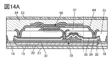
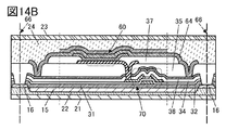
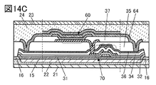
- 14A to 14C are cross-sectional views illustrating an example of a method for manufacturing a light-emitting device.
- 15A to 15D are cross-sectional views illustrating an example of a method for manufacturing a light-emitting device.
- 16A and 16B are cross-sectional views illustrating an example of a method for manufacturing a light-emitting device.
- 17A and 17B are cross-sectional views illustrating an example of a method for manufacturing a light-emitting device.
- 18A to 18C are cross-sectional views illustrating an example of a method for manufacturing a light-emitting device.
- FIG. 19A is a top view illustrating an example of a light emitting device.
- FIG. 19A is a top view illustrating an example of a light emitting device.
- FIG. 19B is a cross-sectional view illustrating an example of a light emitting device.
- 20A and 20B are cross-sectional views illustrating an example of a light emitting device.
- FIG. 21A is a top view illustrating an example of a light emitting device.
- FIG. 21B is a cross-sectional view illustrating an example of a light emitting device.
- FIG. 22 is a cross-sectional view illustrating an example of a light emitting device.
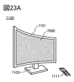
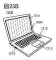
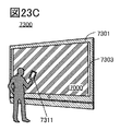
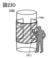
- FIGS. 23A to 23D are diagrams each illustrating an example of an electronic device.
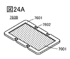
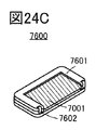
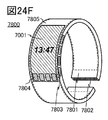
- 24A to 24F are diagrams illustrating an example of an electronic device.
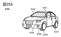
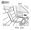
- FIGS. 25A to 25C are diagrams each illustrating an example of an electronic device.
- the word “film” and the word “layer” can be interchanged with each other depending on the case or the situation.
- the term “conductive layer” can be changed to the term “conductive film”.
- the term “insulating film” can be changed to the term “insulating layer”.
- a plurality of light-emitting devices is divided for each light-emitting device by dividing a region where an inorganic film extending over a light-emitting portion is not provided.
- a crack occurs in the inorganic film during the outer shape processing of the light emitting device, it is possible to suppress the crack from spreading to the light emitting portion.
- the light-emitting device of one embodiment of the present invention is flexible and includes a light-emitting element, a first inorganic insulating layer, a second inorganic insulating layer, and a first organic insulating layer.
- the first organic insulating layer is located on the first inorganic insulating layer
- the light emitting element is located on the first inorganic insulating layer via the first organic insulating layer
- the second inorganic insulating layer is emitting light.
- the end of the first inorganic insulating layer and the end of the second inorganic insulating layer are each located inside the end of the first organic insulating layer. An end of the first organic insulating layer is exposed on a side surface of the light emitting device.
- the light-emitting device of one embodiment of the present invention is manufactured by dividing a region where an inorganic film extending to a light-emitting portion is not provided, an organic film is mainly exposed on a side surface of the light-emitting device.
- the organic film since the organic film has lower waterproofness than the inorganic film, impurities such as water may easily enter the inside of the light emitting device from the side surface of the light emitting device. Therefore, it is preferable that the first inorganic insulating layer and the second inorganic insulating layer be in contact with each other outside the end portion of the light emitting element.
- the first organic insulating layer preferably has an opening outside the end portion of the light-emitting element, and in the opening, the first inorganic insulating layer and the second inorganic insulating layer are preferably in contact with each other.
- the two inorganic insulating layers By surrounding the light-emitting element with the two inorganic insulating layers, a structure in which the impurity hardly reaches the light-emitting element even when the impurity enters from the side surface of the light-emitting device can be obtained. Thereby, the reliability of the light emitting device can be improved.
- the light-emitting device of one embodiment of the present invention can be used, for example, as a display device or a lighting device.
- a light-emitting device that can be used as a display device will be mainly described as an example.
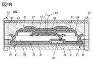
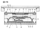
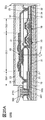
- [Cross-sectional structure of light emitting device] 1A and 1B are cross-sectional views of a light emitting device of the present embodiment.
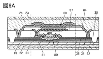
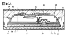
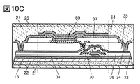
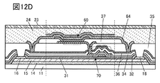
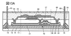
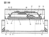
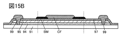
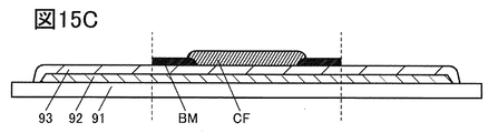
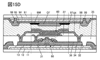
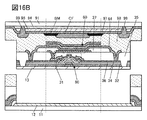
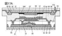
- a light emitting device 10A shown in FIG. 1A includes a substrate 21, an adhesive layer 22, an inorganic insulating layer 31, a transistor 40, an inorganic insulating layer 33, an organic insulating layer 35, a light emitting element 60, a partition 37, an inorganic insulating layer 64, an adhesive layer 24, And a substrate 23.
- the light emitting device 10A has flexibility. Note that the light-emitting device of this embodiment has flexibility. Each of the components of the light-emitting device uses a flexible material.
- the transistor 40 is located on the inorganic insulating layer 31.
- the inorganic insulating layer 33 is located over the transistor 40.
- the organic insulating layer 35 is located on the inorganic insulating layer 33.
- the light emitting element 60 is located on the inorganic insulating layer 31 via the organic insulating layer 35. Further, it can be said that the light emitting element 60 is located on the inorganic insulating layer 33 with the organic insulating layer 35 interposed therebetween.
- an EL element such as an OLED (Organic Light Emitting Diode) or a QLED (Quantum-dot Light Emitting Diode) is preferably used.
- Either an organic compound or an inorganic compound may be used as a light-emitting substance included in the EL element.
- a substance which emits fluorescence (fluorescent material), a substance which emits phosphorescence (phosphorescent material), and a substance which shows heat-activated delayed fluorescence (heat Activation delayed fluorescence (Thermally activated @ delayed * fluorescence: TADF) material, quantum dot material, and the like can be used.
- an LED such as a micro LED (Light Emitting Diode) can be used as the light-emitting element 60.
- a case where an EL element is used as the light-emitting element 60 will be mainly described as an example.
- the light-emitting element 60 includes an electrode 61, an EL layer 62, and an electrode 63.
- the EL layer 62 is located between the electrode 61 and the electrode 63.
- the EL layer 62 contains at least a light emitting substance.
- the electrode 63 has a function of transmitting visible light.
- the electrode 61 preferably has a function of reflecting visible light.
- the light emitting element 60 has a function of emitting visible light.
- the light emitting element 60 is an electroluminescent element that emits light toward the substrate 23 by applying a voltage between the electrode 61 and the electrode 63 (see Light Emission 20). That is, the light emitting device 10A has a top emission structure.
- the light-emitting device of one embodiment of the present invention may be any of a top emission type, a bottom emission type, and a dual emission type.
- a conductive film that transmits visible light is used for the electrode from which light is extracted. It is preferable to use a conductive film that reflects visible light for the electrode on the side from which light is not extracted.
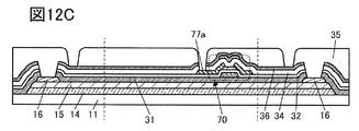
- the electrode 61 is electrically connected to a source or a drain included in the transistor 40 through an opening provided in the inorganic insulating layer 33 and the organic insulating layer 35.
- the electrode 61 has a function as a pixel electrode.
- the end of the electrode 61 is covered with the partition 37.
- the partition wall 37 may use either an inorganic insulating layer or an organic insulating layer.
- an organic insulating layer it is preferable that the inorganic insulating layer 64 be provided so as to cover the side surface of the partition 37.
- an inorganic insulating layer it is preferable that the partition wall 37 and the inorganic insulating layer 64 be in contact with each other outside the end of the electrode 63.
- a protective layer so as to cover the light emitting element 60.
- the protective layer By providing the protective layer, entry of impurities such as water into the light-emitting element 60 can be suppressed, and reliability of the light-emitting element 60 can be improved.
- the protective layer preferably has at least one inorganic film.
- an example including an inorganic insulating layer 64 as a protective layer is described.
- the protective layer may have a laminated structure of an inorganic film and an organic film.
- the stacked structure for example, a structure in which a silicon oxynitride film, a silicon oxide film, an organic film, a silicon oxide film, and a silicon nitride film are sequentially formed is given.
- impurities typically, hydrogen, water, or the like
- the protective layer and the substrate 23 are bonded to each other by the adhesive layer 24.
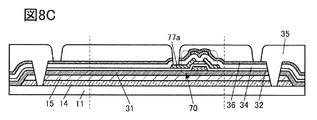
- An end of the organic insulating layer 35 is exposed on a side surface of the light emitting device 10A.
- the end of the inorganic insulating layer 31, the end of the inorganic insulating layer 33, and the end of the inorganic insulating layer 64 are each located inside the end of the organic insulating layer 35.
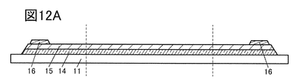
- the side surface of the light emitting device 10A is a surface that is exposed by dividing for processing the outer shape in the manufacturing process of the light emitting device 10A. Since the inorganic insulating layer 31, the inorganic insulating layer 33, and the inorganic insulating layer 64 are not provided in the region 50 including the side surface of the light emitting device 10A, generation of cracks in these layers due to division can be suppressed. Therefore, even if the light emitting device 10A is held in a bent state for a long time or is repeatedly bent, a crack is hardly generated inside the light emitting device 10A, and even if the crack is generated, it does not easily progress. Thereby, the bending resistance of the light emitting device 10A can be increased.
- the region 50 including the side surface of the light emitting device 10A includes the substrate 21, the adhesive layer 22, the organic insulating layer 35, the adhesive layer 24, and the substrate 23.
- Each of these layers preferably contains an organic material.
- the organic material has lower waterproofness than the inorganic material, impurities such as water may enter the light emitting device 10A from the side surface of the light emitting device 10A through the region 50. Therefore, it is preferable that the inorganic insulating layers be in contact with each other outside the end portion of the transistor 40 (at least the end portion of the semiconductor layer where a channel is formed) and inside the region 50. It is preferable that the inorganic insulating layers be in contact with each other outside and inside the region 50 (see the region 51).
- the region 51 makes it difficult for the impurity to reach the light emitting element 60 and the transistor 40. Thereby, the reliability of the light emitting device 10A can be improved.
- the inorganic insulating layer 31 and the inorganic insulating layer 33 are in contact with each other.
- the inorganic insulating layer 33 and the inorganic insulating layer 64 are in contact with each other through an opening provided in the organic insulating layer 35.
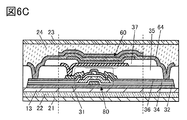
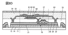
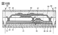
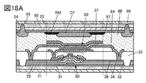
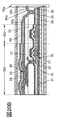
- a light emitting device 10B shown in FIG. 1B has an organic insulating layer 39 in addition to the configuration of the light emitting device 10A.
- the organic insulating layer 39 covers the end of the inorganic insulating layer 31 and the end of the inorganic insulating layer 33, and the end of the organic insulating layer 39 is exposed on the side surface of the light emitting device 10B.
- the organic insulating layer 35 is located on the organic insulating layer 39.
- a region 50 including the side surface of the light emitting device 10B includes the substrate 21, the adhesive layer 22, the organic insulating layer 39, the organic insulating layer 35, the adhesive layer 24, and the substrate 23.
- the laminated structure from the inorganic insulating layer 31 to the substrate 23 is formed over a supporting substrate (not shown) via a release layer, separated from the supporting substrate, and transferred to the substrate 21.
- the separation interface may be different between the region 50 and another region.
- the organic insulating layer 35 may be damaged by a process of reducing the adhesion at the interface (heating or laser beam irradiation).
- the organic insulating layer 35 has a function as a planarizing layer, a function as a layer supporting the light-emitting element 60, and the like, damage to the organic insulating layer 35 may reduce the reliability of the light-emitting device. is there. Therefore, it is preferable that the organic insulating layer 39 be provided in the region 50 and be separated at the interface between the organic insulating layer 39 and the separation layer.
- the organic insulating layer 39 is preferably formed of a material different from that of the organic insulating layer 35. Specifically, it is preferable to select a material for the organic insulating layer 39 so that the removability in the region 50 is high.
- the releasability can be improved by locating the organic insulating layer 39 as compared with the case where the organic insulating layer 35 is located at the separation interface.
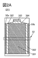
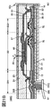
- Each light emitting device includes a light emitting unit 381, a circuit 382, an external connection terminal 383, and a wiring unit 384.
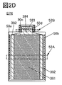
- the light-emitting device EP1 illustrated in FIG. 2A includes a pair of regions (a region 50a and a region 50b) provided so as to sandwich the light-emitting portion 381.
- the light emitting device EP1 can be bent, for example, in the region 52. In the region 52, the light emitting device EP1 can be bent along a line passing through three portions of the region 50a, the region 50b, and the light emitting portion 381.
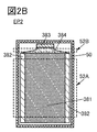
- the light-emitting device EP2 illustrated in FIG. 2B includes a region 50 provided so as to surround the light-emitting portion 381, the circuit 382, the external connection terminal 383, and the wiring portion 384.
- the light emitting device EP2 can be bent, for example, in the region 52A and the region 52B.
- the light emitting device EP2 can be bent along a line passing through two positions of the region 50 and the light emitting portion 381 in total. Two portions of the region 50 are located so as to sandwich the light emitting unit 381. Further, the light emitting device EP2 can be bent along a line passing through two places in the area 50 and the wiring part 384 in the area 52B. Two portions of the region 50 are located so as to sandwich the wiring portion 384.
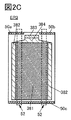
- the light-emitting device EP3 illustrated in FIG. 2C includes a region 50a, a region 50b, and a region 50c.
- the region 50a and the region 50c are provided so as to sandwich the light emitting unit 381 and the wiring unit 384, and the region 50b and the region 50c are provided so as to sandwich the light emitting unit 381 and the wiring unit 384.
- the light emitting device EP3 can be bent, for example, in two regions 52. In each region 52, the light emitting device EP3 can be bent along a line passing through four regions: the region 50a or the region 50b, the region 50c, the wiring portion 384, and the light emitting portion 381.
- the light emitting device EP4 illustrated in FIG. 2D includes a pair of regions (regions 50a and 50b) provided so as to sandwich the light emitting unit 381 and a pair of regions (regions 50c and 50d) provided so as to sandwich the wiring unit 384. ).
- the light emitting device EP4 can be bent, for example, in the region 52A and the region 52B.
- the light emitting device EP4 can be bent along a line passing through three portions of the region 50a, the region 50b, and the light emitting portion 381.
- the light emitting device EP4 can be bent along a line passing through three portions of the region 50c, the region 50d, and the wiring portion 384.
- the same configuration as the light emitting device 10A (FIG. 1A) or the light emitting device 10B (FIG. 1B) can be applied to the region 50 and the regions 50a to 50d shown in FIGS. 2A to 2D, respectively. That is, it can be said that the region 50 and the regions 50a to 50d are regions where the inorganic film extending to the light-emitting portion 381 and the wiring portion 384 is not provided. Therefore, generation and progress of cracks can be suppressed by bending the light emitting device so as to include these regions. Thereby, the bending resistance of the light emitting device can be increased.
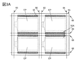
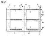
- 3A and 3B show top views of a large-sized panel 55 including four light emitting devices EP.
- the light emitting device EP can be divided into one.
- the dividing line 66 preferably passes through the region 50.
- the region 50 is a region where the inorganic film extending to the light emitting portion is not provided.
- the division line 66 By causing the division line 66 to pass through the region 50, it is possible to suppress the occurrence of cracks in the light emitting device EP at the time of division.
- the adjacent regions 50A shown in FIG. 3A may be connected like the region 50B shown in FIG. 3B. Thereby, the number of dividing lines can be reduced, and the dividing step can be shortened. Further, the area of the dividing part can be reduced, and the area of the light emitting part can be enlarged.
- a thin film (an insulating film, a semiconductor film, a conductive film, or the like) included in the light-emitting device is formed by a sputtering method, a chemical vapor deposition (CVD) method, a vacuum deposition method, or a pulsed laser deposition (PLD: Pulsed Laser Deposition). ), Atomic layer deposition (ALD: Atomic Layer Deposition), or the like.
- CVD chemical vapor deposition
- ALD Atomic layer deposition
- the CVD method include a plasma enhanced chemical vapor deposition (PECVD) method and a thermal CVD method.
- PECVD plasma enhanced chemical vapor deposition
- thermal CVD there is a metal organic chemical vapor deposition (MOCVD) method.
- thin films constituting the light emitting device include spin coating, dip, spray coating, inkjet, dispensing, screen printing, offset printing, doctor knife, slit coating, roll coating, and curtain coating. , A knife coat or the like.
- the thin film when a thin film included in a light emitting device is processed, the thin film can be processed using a photolithography method or the like.
- a thin film may be processed by a nanoimprint method, a sand blast method, a lift-off method, or the like.
- an island-shaped thin film may be directly formed by a film formation method using a shielding mask such as a metal mask.
- the photolithography method there are typically the following two methods.
- One is a method of forming a resist mask on a thin film to be processed, processing the thin film by etching or the like, and removing the resist mask.
- the other is a method in which after forming a thin film having photosensitivity, exposure and development are performed to process the thin film into a desired shape.
- light used for exposure can be, for example, i-line (365 nm in wavelength), g-line (436 nm in wavelength), h-line (405 nm in wavelength), or a mixture of these.
- ultraviolet light, KrF laser light, ArF laser light, or the like can be used.
- the exposure may be performed by a liquid immersion exposure technique.
- extreme ultraviolet light EUV: Extreme-Ultra-violet
- X-ray may be used as light used for exposure.
- an electron beam can be used instead of light used for exposure. It is preferable to use extreme ultraviolet light, X-rays, or an electron beam because extremely fine processing can be performed.
- a photomask is not required.
- a dry etching method for the etching of the thin film, a dry etching method, a wet etching method, a sand blast method, or the like can be used.
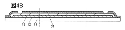
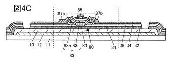
- an island-shaped metal oxide layer 12 is formed on a support substrate 11, an island-shaped resin layer 13 is formed on the metal oxide layer 12, and an inorganic insulating layer 31 is formed on the support substrate 11 and the resin layer 13. (FIG. 4A).
- Example 1 an example in which separation is performed at the interface between the metal oxide layer 12 and the resin layer 13 is described.
- a heat treatment in an atmosphere containing oxygen at the time of forming the resin layer 13 and irradiation of the resin layer 13 with a laser beam can be given.
- at least one of the heat treatment and the irradiation with the laser light is preferably performed. In some cases, separation occurs in the weakened resin layer 13.
- a linear laser beam When irradiating the entire surface of the resin layer 13 with laser light, it is preferable to use a linear laser beam.
- a laser an excimer laser, a solid-state laser, or the like can be used.
- DPSS diode-pumped solid-state laser
- a laser device of a production line such as a low-temperature polysilicon (LTPS (Low Temperature, Poly-Silicon)) or the like can be used, so that these devices can be effectively used.
- LTPS Low Temperature, Poly-Silicon
- a substrate is turned upside down, and a laser beam is emitted from directly above with the support substrate 11 side as a surface, so that the laser beam irradiation in one embodiment of the present invention is performed. It can be diverted to the process.
- An existing LTPS production line can be applied to a production line of a top-gate type self-aligned transistor using an oxide semiconductor (OS). As described above, the existing LTPS manufacturing facility can be easily switched to a manufacturing facility having the separation step of one embodiment of the present invention and the OS transistor manufacturing step.
- OS oxide semiconductor
- a step of irradiating the entire surface of the resin layer 13 with a laser beam can be reduced.
- a laser device for irradiating a linear laser beam is expensive in itself and has a high running cost. According to one embodiment of the present invention, the laser device is unnecessary, so that cost can be significantly reduced. Further, application to a large-sized substrate is easy.
- the heat treatment can enhance the releasability of the resin layer 13. Even if foreign matter adheres to the support substrate 11, unevenness in heating hardly occurs in the resin layer 13, so that the yield of the step of separating the support substrate 11 from the resin layer 13 does not easily decrease.
- the metal oxide layer 12 and the inorganic insulating layer 31 may have low adhesion depending on the material. If the adhesion between the metal oxide layer 12 and the inorganic insulating layer 31 is low, unintentional peeling (peeling) may occur during the manufacturing process of the light emitting device, and the yield may be reduced. For example, when a titanium oxide film is used for the metal oxide layer 12 and an inorganic insulating film such as a silicon oxide film or a silicon oxynitride film is used for the inorganic insulating layer 31, film peeling may be observed. Therefore, it is preferable to provide the resin layer 13 so as to cover the upper surface and the side surfaces of the metal oxide layer 12.
- the metal oxide layer 12 and the resin layer 13 are provided in an island shape, and the inorganic insulating layer 31 is provided so as to cover an end of the island-shaped metal oxide layer 12 and an end of the island-shaped resin layer 13. Is preferred. If the metal oxide layer 12 and the resin layer 13 are provided on one entire surface of the support substrate 11, the resin layer 13 may be unintentionally peeled off from the metal oxide layer 12. Therefore, it is preferable to provide a region where the inorganic insulating layer 31 is in contact with the support substrate 11. This can prevent the resin layer 13 from being unintentionally peeled off from the metal oxide layer 12. By forming the starting point of the separation, the timing of the separation can be controlled, and the metal oxide layer 12 and the resin layer 13 can be separated at a desired timing.
- the support substrate 11 has rigidity to such an extent that it can be easily transported, and has heat resistance to the temperature required for the manufacturing process.
- a material that can be used for the supporting substrate 11 include glass, quartz, ceramic, sapphire, resin, semiconductor, metal, and alloy.
- the glass include non-alkali glass, barium borosilicate glass, and aluminoborosilicate glass.
- an underlayer is formed between the support substrate 11 and the resin layer 13.
- the base layer may have either a single-layer structure or a stacked structure, and one or both of a metal layer and a metal oxide layer can be used.
- the base layer includes titanium, molybdenum, aluminum, tungsten, silicon, indium, zinc, gallium, tantalum, tin, hafnium, yttrium, zirconium, magnesium, lanthanum, cerium, neodymium, bismuth, and niobium.
- the underlayer can include metals, alloys, and compounds thereof (eg, metal oxides).
- the base layer preferably contains one or more of titanium, molybdenum, aluminum, tungsten, silicon, indium, zinc, gallium, tantalum, and tin.
- metal oxide layer 12 Various metal oxides can be used for the metal oxide layer 12.
- the metal oxide include titanium oxide (TiO x ), molybdenum oxide, aluminum oxide, tungsten oxide, indium tin oxide containing silicon (ITSO), indium zinc oxide, and In—Ga—Zn oxide.
- metal oxides include indium oxide, indium oxide containing titanium, indium oxide containing tungsten, indium tin oxide (ITO), ITO containing titanium, indium zinc oxide containing tungsten, and zinc oxide (ZnO). ), Gallium-containing ZnO, hafnium oxide, yttrium oxide, zirconium oxide, gallium oxide, tantalum oxide, magnesium oxide, lanthanum oxide, cerium oxide, neodymium oxide, tin oxide, bismuth oxide, titanate, tantalate, niobate And the like.
- the metal oxide layer 12 can be formed by introducing oxygen into the metal layer. At this time, only the surface of the metal layer or the entire metal layer is oxidized. In the former case, a stacked structure of a metal layer and a metal oxide layer is formed by introducing oxygen into the metal layer.
- the metal layer can be oxidized by heating the metal layer in an atmosphere containing oxygen. It is preferable to heat the metal layer while flowing a gas containing oxygen.
- the temperature at which the metal layer is heated is preferably from 100 ° C to 500 ° C, more preferably from 100 ° C to 450 ° C, more preferably from 100 ° C to 400 ° C, and even more preferably from 100 ° C to 350 ° C.
- the metal layer be heated at a temperature equal to or lower than the maximum temperature in manufacturing the transistor.
- the temperature of the heat treatment is preferably 350 ° C or lower.
- the metal layer can be oxidized by performing a radical treatment on the surface of the metal layer.
- the radical treatment the surface of the metal layer is preferably exposed to an atmosphere containing at least one of an oxygen radical and a hydroxyl radical.
- plasma treatment is preferably performed in an atmosphere containing one or both of oxygen and water vapor (H 2 O).
- the metal oxide layer 12 and the resin layer 13 can be reduced. For this reason, it is preferable to perform a radical treatment or a plasma treatment for forming the metal oxide layer 12.
- the metal layer is oxidized by performing a radical treatment or a plasma treatment on the surface of the metal layer, a step of heating the metal layer at a high temperature becomes unnecessary. Therefore, it is possible to prevent the maximum temperature in manufacturing the light emitting device from increasing.
- the metal oxide layer 12 can be formed in an oxygen atmosphere.
- the metal oxide layer 12 can be formed by forming a metal oxide film by a sputtering method while flowing a gas containing oxygen.
- the radical treatment the surface of the metal oxide layer 12 is preferably exposed to an atmosphere containing at least one of oxygen radicals, hydrogen radicals, and hydroxy radicals.
- plasma treatment is preferably performed in an atmosphere containing one or more of oxygen, hydrogen, and water vapor (H 2 O).
- the radical treatment can be performed using a plasma generator or an ozone generator.
- oxygen plasma treatment hydrogen plasma treatment, water plasma treatment, ozone treatment, or the like can be performed.
- the oxygen plasma treatment can be performed by generating plasma in an atmosphere containing oxygen.
- the hydrogen plasma treatment can be performed by generating plasma in an atmosphere containing hydrogen.
- the water plasma treatment can be performed by generating plasma in an atmosphere containing water vapor (H 2 O). In particular, by performing the water plasma treatment, a large amount of moisture can be contained on the surface or inside of the metal oxide layer 12, which is preferable.
- Plasma treatment may be performed in an atmosphere containing two or more of oxygen, hydrogen, water (steam), and an inert gas (typically, argon).
- an inert gas typically, argon
- the plasma treatment for example, plasma treatment in an atmosphere containing oxygen and hydrogen, plasma treatment in an atmosphere containing oxygen and water, plasma treatment in an atmosphere containing water and argon, oxygen and argon Plasma treatment in an atmosphere containing oxygen, water, and argon, and the like.
- the use of an argon gas as one of the plasma treatment gases is preferable because the plasma treatment can be performed while damaging the metal layer or the metal oxide layer 12.
- Two or more kinds of plasma treatments may be performed continuously without exposure to the atmosphere.
- water plasma treatment may be performed after argon plasma treatment.
- an ion implantation method As a method for introducing oxygen, hydrogen, water, or the like, an ion implantation method, an ion doping method, a plasma immersion ion implantation method, or the like can be used.
- the thickness of the metal layer is preferably from 1 nm to 100 nm, more preferably from 1 nm to 50 nm, and still more preferably from 1 nm to 20 nm.
- the thickness of the metal oxide layer 12 is, for example, preferably from 1 nm to 200 nm, more preferably from 5 nm to 100 nm, and still more preferably from 5 nm to 50 nm.
- the thickness of the finally formed metal oxide layer 12 may be larger than the thickness of the formed metal layer.
- the metal oxide layer 12 is preferably made of titanium oxide, tungsten oxide, or the like.
- the use of titanium oxide is preferable because the cost can be reduced as compared with that of tungsten oxide.
- the resin layer 13 can be formed using various resin materials (including a resin precursor).
- the resin layer 13 is preferably formed using a thermosetting material.
- the resin layer 13 may be formed using a photosensitive material or a non-photosensitive material (also referred to as a non-photosensitive material).
- a photosensitive material also referred to as a non-photosensitive material
- the resin layer 13 having a desired shape can be formed by a lithography method using light.
- the resin layer 13 may have an opening or an uneven shape.
- the resin layer 13 is preferably formed using a material containing a polyimide resin, a polyimide resin precursor, or an acrylic resin.
- the resin layer 13 can be formed using, for example, a material containing a polyimide resin and a solvent, a material containing a polyamic acid and a solvent, or a material containing an acrylic resin and a solvent.
- a material containing a polyimide resin or a polyimide resin precursor is preferable because of its relatively high heat resistance.
- a material containing an acrylic resin is preferable because it has high transparency to visible light. Since the polyimide resin and the acrylic resin are each a material suitably used for a flattening film or the like of a light emitting device, a film forming device and a material can be shared.
- the resin layer 13 does not require a special material and can be formed using a resin material used for a light-emitting device; therefore, cost can be suppressed.
- examples of the resin material that can be used for forming the resin layer 13 include an epoxy resin, a polyamide resin, a polyimide amide resin, a siloxane resin, a benzocyclobutene-based resin, a phenol resin, and a precursor of these resins.
- the heat treatment can be performed, for example, while flowing a gas containing one or more of oxygen, nitrogen, and a rare gas (such as argon) into a chamber of a heating device.
- a gas containing one or more of oxygen, nitrogen, and a rare gas such as argon
- the heat treatment can be performed in an air atmosphere using a chamber of a heating device, a hot plate, or the like.
- Heating is preferably performed while flowing nitrogen gas. This makes it possible to reduce the amount of oxygen contained in the heating atmosphere as compared with the air atmosphere, suppress oxidation of the resin layer 13, and increase the transparency of the resin layer 13 to visible light.
- heating is preferably performed in an air atmosphere.
- heating is preferably performed while flowing a gas containing oxygen.
- the resin layer 13 contains more oxygen, the force required to separate the metal oxide layer 12 and the resin layer 13 can be reduced.
- heating is preferably performed in an atmosphere containing oxygen.
- degassed components eg, hydrogen, water, and the like
- the film to be the resin layer 13 is preferably heated at 350 ° C. to 450 ° C., more preferably 400 ° C. or less, and even more preferably 375 ° C. or less. Accordingly, outgassing from the resin layer 13 in a transistor manufacturing process can be significantly suppressed.
- the temperature of the heat treatment is preferably lower than or equal to the highest temperature in manufacturing the transistor.
- a manufacturing apparatus or the like in the manufacturing process of the transistor can be used, so that additional capital investment can be suppressed. Therefore, a light emitting device with reduced production cost can be provided.
- the temperature of the heat treatment is preferably 350 ° C or lower.
- the maximum temperature in manufacturing the transistor is equal to the temperature of the heat treatment
- the maximum temperature in the manufacture of the light-emitting device can be prevented from increasing by performing heat treatment, and the outgassing component of the resin layer 13 can be reduced. preferable.
- the heat treatment time is, for example, preferably from 5 minutes to 24 hours, more preferably from 30 minutes to 12 hours, even more preferably from 1 hour to 6 hours. Note that the time of the heat treatment is not limited to this. For example, in a case where the heat treatment is performed using an RTA (Rapid Thermal Annealing) method, the heat treatment may be performed for less than 5 minutes.
- RTA Rapid Thermal Annealing
- the heating device various devices such as an electric furnace and a device for heating an object to be processed by heat conduction or heat radiation from a heating element such as a resistance heating element can be used.
- an RTA device such as a GRTA (Gas Rapid Thermal Anneal) device and an LRTA (Lamp Rapid Thermal Anneal) device can be used.
- the LRTA apparatus is an apparatus that heats an object to be processed by radiation of light (electromagnetic waves) emitted from a lamp such as a halogen lamp, a metal halide lamp, a xenon arc lamp, a carbon arc lamp, a high-pressure sodium lamp, and a high-pressure mercury lamp.
- the GRTA apparatus is an apparatus that performs a heat treatment using a high-temperature gas.
- the use of the RTA apparatus can reduce the processing time, which is preferable for mass production.
- the heat treatment may be performed using an in-line heating device.
- heat treatment for removing a solvent contained in the film to be the resin layer 13 may be performed.
- the temperature of the pre-bake treatment can be appropriately determined according to the material used.
- the heat treatment can be performed at a temperature of 50 to 180 ° C, 80 to 150 ° C, or 90 to 120 ° C.
- the heat treatment may also serve as a pre-bake treatment, and the solvent may be removed by the heat treatment.
- the resin layer 13 has flexibility.
- the support substrate 11 has lower flexibility than the resin layer 13.
- the thickness of the resin layer 13 is preferably 0.01 ⁇ m or more and less than 10 ⁇ m, more preferably 0.1 ⁇ m or more and 5 ⁇ m or less, and even more preferably 0.5 ⁇ m or more and 3 ⁇ m or less.
- a light-emitting device can be manufactured at low cost. Further, the weight and thickness of the light emitting device can be reduced. Further, the flexibility of the light emitting device can be increased. By using a low-viscosity solution, it becomes easy to form the resin layer 13 thin.
- the thickness is not limited to this, and the thickness of the resin layer 13 may be 10 ⁇ m or more.
- the thickness of the resin layer 13 may be not less than 10 ⁇ m and not more than 200 ⁇ m. It is preferable that the thickness of the resin layer 13 be 10 ⁇ m or more, since the rigidity of the light emitting device can be increased.
- the coefficient of thermal expansion of the resin layer 13 is preferably from 0.1 ppm / ° C to 50 ppm / ° C, more preferably from 0.1 ppm / ° C to 20 ppm / ° C, and more preferably from 0.1 ppm / ° C to 10 ppm / ° C. It is more preferable that the temperature is not higher than ° C. As the coefficient of thermal expansion of the resin layer 13 is lower, the occurrence of cracks in the layers included in the transistor and the like due to heating and the damage to the transistor and the like can be suppressed.
- the inorganic insulating layer 31 preferably has a function of blocking hydrogen, oxygen, and water released from the metal oxide layer 12, the resin layer 13, and the like in a subsequent heating step.
- the inorganic insulating layer 31 is formed at a temperature equal to or lower than the heat resistant temperature of the resin layer 13.
- the film is preferably formed at a temperature lower than the temperature of the heat treatment.
- an inorganic insulating film such as a silicon nitride film, a silicon oxynitride film, a silicon oxide film, a silicon nitride oxide film, an aluminum oxide film, and an aluminum nitride film can be used.
- a hafnium oxide film, an yttrium oxide film, a zirconium oxide film, a gallium oxide film, a tantalum oxide film, a magnesium oxide film, a lanthanum oxide film, a cerium oxide film, a neodymium oxide film, or the like may be used.
- two or more of the above insulating films may be stacked and used.
- silicon oxynitride refers to a component whose content of oxygen is higher than that of nitrogen.
- silicon nitride oxide refers to a substance having a higher nitrogen content than oxygen as its composition.
- the inorganic insulating layer 31 is preferably formed at a high temperature because the higher the deposition temperature, the denser the film and the higher the barrier property.
- the substrate temperature at the time of forming the inorganic insulating layer 31 is preferably from room temperature (25 ° C.) to 350 ° C., more preferably from 100 ° C. to 300 ° C.
- an opening is formed in the inorganic insulating layer 31 at a position overlapping the metal oxide layer 12 and the resin layer 13 (FIG. 4B).
- the step of forming an opening in the inorganic insulating layer 31 may be performed before the formation of the organic insulating layer 35, and can be performed before, during, or after formation of the transistor 80.
- the transistor 80 is formed over the inorganic insulating layer 31 (FIG. 4C).
- the structure of the transistor included in the light-emitting device is not particularly limited.
- a planar transistor, a staggered transistor, or an inverted staggered transistor may be used.
- a top gate structure or a bottom gate structure may be employed.
- gate electrodes may be provided above and below a channel.
- crystallinity of a semiconductor material used for the transistor there is no particular limitation on the crystallinity of a semiconductor material used for the transistor, either an amorphous semiconductor or a semiconductor having crystallinity (a microcrystalline semiconductor, a polycrystalline semiconductor, a single crystal semiconductor, or a semiconductor partially having a crystalline region). May be used. It is preferable to use a semiconductor having crystallinity because deterioration of transistor characteristics can be suppressed.
- the semiconductor layer of the transistor preferably includes a metal oxide (also referred to as an oxide semiconductor).
- the semiconductor layer of the transistor may include silicon. Examples of silicon include amorphous silicon and crystalline silicon (such as low-temperature polysilicon and single-crystal silicon).
- an oxide semiconductor is used as a semiconductor of the transistor. It is preferable to use a semiconductor material having a wider band gap and a smaller carrier density than silicon because current in an off state of the transistor can be reduced.
- the transistor 80 is formed at a temperature lower than the allowable temperature limit of the resin layer 13.
- the transistor 80 is preferably formed at a temperature lower than the temperature of the heat treatment at the time of forming the resin layer 13.
- a conductive layer 81 functioning as a gate electrode is formed over the inorganic insulating layer 31.
- the conductive layer 81 can be formed by forming a conductive film, forming a resist mask, etching the conductive film, and removing the resist mask.
- the conductive layer included in the light-emitting device has a single-layer structure of a metal such as aluminum, titanium, chromium, nickel, copper, yttrium, zirconium, molybdenum, silver, tantalum, or tungsten, or an alloy containing this as a main component or It can be used as a laminated structure.
- a metal such as aluminum, titanium, chromium, nickel, copper, yttrium, zirconium, molybdenum, silver, tantalum, or tungsten, or an alloy containing this as a main component or It can be used as a laminated structure.
- a metal such as aluminum, titanium, chromium, nickel, copper, yttrium, zirconium, molybdenum, silver, tantalum, or tungsten, or an alloy containing this as a main component or It can be used as a laminated structure.
- a semiconductor such as polycrystalline silicon or an oxide semiconductor, or a silicide such as nickel silicide, which has a low resistance by containing an impurity element or the like, may be used.
- a film containing graphene can be used. The film containing graphene can be formed by, for example, reducing a film containing graphene oxide.
- a semiconductor such as an oxide semiconductor containing an impurity element may be used.
- the conductive paste may be formed using a conductive paste such as silver, carbon, or copper, or a conductive polymer such as polythiophene. Conductive pastes are inexpensive and preferred. Conductive polymers are preferred because they are easy to apply.
- an insulating layer 32 functioning as a gate insulating layer is formed.
- an inorganic insulating film which can be used for the inorganic insulating layer 31 can be used.
- the metal oxide layer 83 functioning as an oxide semiconductor layer is formed.
- the metal oxide layer 83 can be formed by forming a metal oxide film, forming a resist mask, etching the metal oxide film, and removing the resist mask.
- the metal oxide film includes indium and M (M is gallium, aluminum, silicon, boron, yttrium, tin, copper, vanadium, beryllium, titanium, iron, nickel, germanium, zirconium, molybdenum, lanthanum, cerium, One or more selected from neodymium, hafnium, tantalum, tungsten, and magnesium) and zinc.
- M is preferably one or more selected from aluminum, gallium, yttrium, and tin.
- an oxide containing indium (In), gallium (Ga), and zinc (Zn) (also referred to as IGZO) is preferably used.
- the metal oxide film is an In-M-Zn oxide
- the atomic ratio of the semiconductor layer to be formed includes a variation of ⁇ 40% of the atomic ratio of the metal element included in the sputtering target.
- the metal oxide film when the atomic ratio of In is higher than the atomic ratio of M (for example, Ga), the field-effect mobility of the transistor can be increased, which is preferable.
- M for example, Ga
- oxygen vacancies are less likely to be formed, which is preferable.
- the metal oxide layer 83 may include a plurality of stacked metal oxide films.
- the substrate temperature during the formation of the metal oxide film is preferably 350 ° C. or lower, more preferably room temperature or higher and 200 ° C. or lower, further preferably room temperature or higher and 130 ° C. or lower.
- the metal oxide film can be formed using one or both of an inert gas and an oxygen gas.
- an inert gas and an oxygen gas.
- the flow rate ratio of oxygen (oxygen partial pressure) during the formation of the metal oxide film is preferably 0% or more and 30% or less, and 5% or more and 30% or less. Is more preferable, and 7% or more and 15% or less are still more preferable.
- the energy gap of the metal oxide film is preferably 2 eV or more, more preferably 2.5 eV or more, further preferably 3 eV or more. With the use of a metal oxide film with a wide energy gap, off-state current of a transistor can be reduced.
- the metal oxide film can be formed by a sputtering method.
- a PLD method a PECVD method, a thermal CVD method, an ALD method, a vacuum evaporation method, or the like may be used.
- the insulating layer 34 functioning as a gate insulating layer is formed over the metal oxide layer 83.
- an inorganic insulating film which can be used for the inorganic insulating layer 31 can be used.
- a conductive layer 85 serving as a gate electrode is formed over the insulating layer 34.
- the conductive layer 85 can be formed by forming a conductive film, forming a resist mask, etching the conductive film, and removing the resist mask.
- an impurity element is supplied to the metal oxide layer 83 to form a low-resistance region 83n.
- a region overlapping with the conductive layer 85 (a channel formation region 83i) is not supplied with an impurity element.
- a plasma ion doping method or an ion implantation method can be preferably used. These methods can control the concentration profile in the depth direction with high accuracy by the ion acceleration voltage, the dose, and the like. By using the plasma ion doping method, productivity can be increased. Further, by using an ion implantation method using mass separation, the purity of a supplied impurity element can be increased.
- the impurity element examples include hydrogen, boron, carbon, nitrogen, fluorine, phosphorus, sulfur, arsenic, aluminum, magnesium, silicon, and a rare gas. It is preferable to use boron, phosphorus, aluminum, magnesium, or silicon as the impurity element, and it is more preferable to use boron or phosphorus.
- a gas containing the above impurity element can be used.
- a B 2 H 6 gas, a BF 3 gas, or the like can be used.
- a phosphorus PH 3 gas can be typically used.
- a mixed gas obtained by diluting these source gases with a rare gas may be used.
- the raw material gas CH 4, N 2, NH 3, AlH 3, AlCl 3, SiH 4, Si 2 H 6, F 2, HF, H 2, (C 5 H 5) 2 Mg, and a rare gas, etc.
- the ion source is not limited to a gas, and a solid or a liquid may be heated and vaporized.
- an impurity element can be supplied by generating plasma in a gas atmosphere containing the impurity element to be supplied and performing plasma treatment.
- a dry etching apparatus As an apparatus for generating the plasma, a dry etching apparatus, an ashing apparatus, a plasma CVD apparatus, a high-density plasma CVD apparatus, or the like can be used.
- the impurity element can be supplied to the metal oxide layer 83 through the insulating layer 34. This can prevent the crystallinity of the metal oxide layer 83 from being lowered when the impurity element is supplied. Therefore, it is particularly suitable when the electric resistance increases due to the decrease in crystallinity.
- an inorganic insulating layer 36 which covers the metal oxide layer 83, the insulating layer 34, and the conductive layer 85 is formed.
- the inorganic insulating layer 36 can be formed by a method similar to that of the inorganic insulating layer 31.
- an opening reaching the low resistance region 83n of the metal oxide layer 83 is formed in the insulating layer 34 and the inorganic insulating layer 36.
- a conductive layer 87a and a conductive layer 87b are formed.
- the conductive layers 87a and 87b can be formed by forming a conductive film, forming a resist mask, etching the conductive film, and removing the resist mask.
- the conductive layers 87a and 87b are electrically connected to the low-resistance regions 83n of the metal oxide layer 83 through openings provided in the insulating layer 34 and the inorganic insulating layer 36, respectively.
- the transistor 80 can be manufactured (FIG. 4C).
- an opening reaching the resin layer 13 is formed in the insulating layer 32, the insulating layer 34, and the inorganic insulating layer 36 (FIG. 4C).
- the opening may be formed before the organic insulating layer 35 is formed, and can be formed during or after the transistor 80 is manufactured. Note that the openings may be formed collectively in a plurality of layers, or the openings may be formed for each layer.
- the organic insulating layer 35 is formed over the inorganic insulating layer 36 and the transistor 80 (FIG. 4D).
- the organic insulating layer 35 has a surface on which a light-emitting element to be formed later is formed, and thus preferably functions as a planarization layer.
- Examples of a material that can be used for the organic insulating layer 35 include an acrylic resin, a polyimide resin, an epoxy resin, a polyamide resin, a polyimide amide resin, a siloxane resin, a benzocyclobutene-based resin, a phenol resin, and a precursor of these resins.
- the organic insulating layer 35 is provided so as to fill openings provided in the inorganic insulating layer 31, the insulating layer 32, the insulating layer 34, and the inorganic insulating layer 36, and is in contact with the resin layer 13 through the openings.
- the organic insulating layer 35 is formed so as to have an opening that reaches the inorganic insulating layer 36 inside the opening. Further, the organic insulating layer 35 is formed so as to have an opening reaching the conductive layer 87a.
- an electrode 61 is formed (FIG. 4E).
- a part of the electrode 61 functions as a pixel electrode of the light emitting element 60.
- the electrode 61 can be formed by forming a conductive film, forming a resist mask, etching the conductive film, and removing the resist mask.
- the electrode 61 is electrically connected to the conductive layer 87a through an opening provided in the organic insulating layer 35.
- the partition wall 37 may be formed using either an inorganic material or an organic material.
- an inorganic insulating film that can be used for the inorganic insulating layer 31 can be used.
- a material that can be used for the organic insulating layer 35 can be used.
- an EL layer 62 and an electrode 63 are formed (FIG. 4E).
- a part of the electrode 63 functions as a common electrode of the light emitting element 60.
- the EL layer 62 has at least a light emitting layer.
- the EL layer 62 is a layer other than the light-emitting layer as a substance having a high hole-injection property, a substance having a high hole-transport property, a hole-blocking material, a substance having a high electron-transport property, a substance having a high electron-injection property, or a bipolar property. (A substance having a high electron-transport property and a high hole-transport property) may be further provided.
- Either a low molecular compound or a high molecular compound can be used for the EL layer 62, and the EL layer 62 may contain an inorganic compound.
- the EL layer 62 can be formed by a method such as an evaporation method, a coating method, a printing method, and a discharge method.
- the EL layer 62 can be formed by an evaporation method using a shadow mask such as a metal mask, an inkjet method, or the like.
- an evaporation method without using a metal mask can be used.
- the electrode 63 can be formed by an evaporation method, a sputtering method, or the like.
- the electrode 63 is formed at a temperature lower than the heat resistance temperature of the resin layer 13 and lower than the heat resistance temperature of the EL layer 62.
- the light emitting element 60 can be formed (FIG. 4E).
- an inorganic insulating layer 64 is formed to cover the electrode 63 (FIG. 4E).
- the light emitting element 60 is sealed by the inorganic insulating layer 64.
- the inorganic insulating layer 64 functions as a protective layer that suppresses diffusion of impurities such as water into the light-emitting element 60.
- the protective layer can have a single-layer structure or a stacked structure.
- the protective layer has, for example, a structure including the inorganic insulating layer 64, a structure including two or more layers including the inorganic insulating layer 64, and a structure including two or more layers including the inorganic insulating layer 64 and the organic insulating film. be able to.
- the inorganic insulating layer 64 is connected to the inorganic insulating layer 36 through an opening provided in the organic insulating layer 35. Accordingly, the top, side, and bottom surfaces of the transistor 80 (metal oxide layer 83) and the light-emitting element 60 are surrounded by a plurality of inorganic insulating layers (the inorganic insulating layer 31, the inorganic insulating layer 36, and the inorganic insulating layer 64, and the like). be able to. Therefore, entry of impurities into the transistor 80 and the light-emitting element 60 can be suppressed, and the reliability of the transistor 80 and the light-emitting element 60 can be improved.
- an inorganic insulating film which can be used for the inorganic insulating layer 31 can be used.
- the inorganic insulating layer 64 can be formed by a PECVD method, an ALD method, a sputtering method, or the like.
- the inorganic insulating layer 64 and the substrate 23 are bonded together using the adhesive layer 24 (FIG. 4E).
- curable adhesives such as a photocurable adhesive such as an ultraviolet curable adhesive, a reactive curable adhesive, a thermosetting adhesive, and an anaerobic adhesive can be used. Further, an adhesive sheet or the like may be used.
- the substrate 23 Since the substrate 23 is located on the side from which light from the light emitting element 60 is extracted, it is preferable to use a material having high transparency to visible light. It is preferable to use a film for the substrate 23, and it is particularly preferable to use a resin film. This makes it possible to reduce the weight and thickness of the light emitting device. Further, a light emitting device using a film substrate is less likely to be damaged than a case using glass, metal, or the like. Further, the flexibility of the light emitting device can be increased.
- polyester resin such as polyethylene terephthalate (PET) and polyethylene naphthalate (PEN), polyacrylonitrile resin, acrylic resin, polyimide resin, polymethyl methacrylate resin, polycarbonate (PC) resin, polyether sulfone (PES) ) Resin, polyamide resin (nylon, aramid, etc.), polysiloxane resin, cycloolefin resin, polystyrene resin, polyamideimide resin, polyurethane resin, polyvinyl chloride resin, polyvinylidene chloride resin, polypropylene resin, polytetrafluoroethylene (PTFE) Resin, ABS resin, cellulose nanofiber, or the like can be used.
- the substrate 23 may be made of glass having a thickness enough to have flexibility.
- a substrate having high optical isotropy has a small birefringence (it can be said that the birefringence is small).
- the absolute value of the retardation (phase difference) value of the substrate having high optical isotropy is preferably 30 nm or less, more preferably 20 nm or less, and even more preferably 10 nm or less.
- the film having high optical isotropy examples include a triacetylcellulose (TAC, also referred to as cellulose triacetate) film, a cycloolefin polymer (COP) film, a cycloolefin copolymer (COC) film, and an acrylic film.
- TAC triacetylcellulose
- COP cycloolefin polymer
- COC cycloolefin copolymer
- the film may absorb water to cause a shape change such as wrinkling of the display device. Therefore, it is preferable to use a film having a low water absorption for the substrate.
- a film having a water absorption of 1% or less is preferably used, a film having a water absorption of 0.1% or less is more preferable, and a film having a water absorption of 0.01% or less is more preferable.
- a circularly polarizing plate may be used as a substrate of the display device.
- FIG. 5A shows an example in which a sharp-shaped instrument 65 such as a cutting tool is inserted from the substrate 23 side to the inside of the end of the resin layer 13 to make a cut.
- the cut is preferably formed in a frame shape.
- the starting point of separation may be formed by irradiating a part or the whole of the resin layer 13 with laser light from the support substrate 11 side.
- the metal oxide layer 12 and the resin layer 13 are separated from the starting point of the separation (FIG. 5B).
- the support substrate 11 and the resin layer 13 can be separated.
- the resin layer 13 can be peeled off from the support substrate 11 by adsorbing a part of the upper surface of the substrate 23 and pulling it upward.
- a liquid containing water such as water or an aqueous solution
- the separation interface is added to the separation interface, and the separation is performed so that the liquid permeates the separation interface, whereby the separation can be easily performed.
- static electricity generated at the time of separation can be prevented from adversely affecting a functional element such as a transistor (eg, a semiconductor element is broken by static electricity).
- liquid to be supplied examples include water (preferably pure water), a neutral, alkaline, or acidic aqueous solution, and an aqueous solution in which a salt is dissolved.
- water preferably pure water
- a neutral, alkaline, or acidic aqueous solution examples include water (preferably pure water), a neutral, alkaline, or acidic aqueous solution, and an aqueous solution in which a salt is dissolved.
- ethanol, acetone and the like can be mentioned.
- various organic solvents may be used.
- the substrate 21 is bonded to the exposed resin layer 13 using the adhesive layer 22 (FIG. 6A).
- the transistor 80, the light-emitting element 60, and the like manufactured over the supporting substrate 11 can be transferred from the supporting substrate 11 to the substrate 23.
- the resin layer 13 may be removed, the oxide insulating layer 15 may be exposed, and the oxide insulating layer 15 and the substrate 21 may be bonded.
- the resin layer 13 can be removed by ashing or the like. By removing the resin layer 13, the light emitting device can be made thinner and lighter.
- a material that can be used for the adhesive layer 24 can be used.
- a material that can be used for the substrate 23 can be used.
- various materials such as glass, quartz, resin, metal, alloy, and semiconductor having a thickness enough to have flexibility can be used.
- the light emitting device can be manufactured (FIGS. 6B and 6C).
- the division is performed so that the division line 66 overlaps the openings provided in the inorganic insulating layers 31, 32, 34, and 36. That is, no inorganic film is provided at the dividing position. Therefore, generation of microcracks inside the light emitting device due to the division can be suppressed. Then, even if the light emitting device is held in a bent state for a long time or is repeatedly bent, generation and progress of cracks can be suppressed.
- the top surface, the side surface, and the bottom surface of the transistor 80 (metal oxide layer 83) and the light-emitting element 60 are formed of a plurality of inorganic insulating layers (inorganic layers).
- the insulating layer 31, the inorganic insulating layer 36, the inorganic insulating layer 64, and the like Therefore, entry of impurities into the transistor 80 and the light-emitting element 60 can be suppressed, and the reliability of the transistor 80 and the light-emitting element 60 can be improved.
- Modification 1 will be described with reference to FIG.
- the metal oxide layer 12 is formed as an underlayer between the support substrate 11 and the resin layer 13, but the underlayer may not be provided.
- the resin layer 13 may be formed directly on the support substrate 11 (without interposing an underlayer). Then, as shown in FIG. 7B, a laminated structure from the inorganic insulating layer 31 to the substrate 23 is formed on the resin layer 13.
- the support substrate 11 and the substrate 23 can be separated. In this case, separation occurs at the interface between the support substrate 11 and the resin layer 13 or in the resin layer 13.
- FIG. 7B illustrates an example in which the insulating layer 34 functioning as a gate insulating layer of the transistor 80 is located only between the conductive layer 85 and the metal oxide layer 83.
- the insulating layer 34 may be processed into an island shape using the conductive layer 85 as a mask.
- the inorganic insulating layer 36 preferably contains hydrogen. Hydrogen contained in the inorganic insulating layer 36 diffuses into a region of the metal oxide layer 83 which is in contact with the inorganic insulating layer 36 by heat treatment or the like, so that the region has low resistance and a low-resistance region 83n is formed. it can. In the case where the low-resistance region 83n is formed using the inorganic insulating layer 36, the step of manufacturing the transistor 80 can be reduced in some cases because addition of the above-described impurity element is unnecessary.
- an island-shaped metal layer 14 is formed on the supporting substrate 11, and after a surface treatment of the metal layer 14 is performed, an island-shaped oxide insulating layer 15 is formed. An inorganic insulating layer 31 is formed thereon (FIG. 8A).
- the metal layer 14 and the oxide insulating layer 15 be provided in an island shape, and the inorganic insulating layer 31 be provided so as to cover end portions of the island-shaped metal layer 14 and the island-shaped oxide insulating layer 15.
- the oxide insulating layer 15 may be unintentionally peeled off from the metal layer 14. Therefore, it is preferable to provide a region where the inorganic insulating layer 31 is in contact with the support substrate 11. This can prevent the oxide insulating layer 15 from being unintentionally peeled from the metal layer 14.
- the timing of separation can be controlled, and the metal layer 14 and the oxide insulating layer 15 can be separated at a desired timing.
- an element selected from tungsten (W), molybdenum (Mo), titanium, tantalum, niobium, nickel, cobalt, zirconium, zinc, ruthenium, rhodium, palladium, osmium, iridium, and silicon is used.
- the metal layer 14 has a single-layer structure, it is preferable to form a tungsten layer, a molybdenum layer, or a layer containing a mixture of tungsten and molybdenum.
- a mixture of tungsten and molybdenum corresponds to, for example, an alloy of tungsten and molybdenum.
- the metal layer 14 may be formed by, for example, a sputtering method, a CVD method (plasma CVD method, thermal CVD method, MOCVD method, etc.), an ALD method, a coating method (including a spin coating method, a droplet discharging method, a dispensing method, etc.), a printing method, It can be formed by a vapor deposition method or the like.
- the thickness of the metal layer 14 is from 1 nm to 1000 nm, preferably from 10 nm to 200 nm, more preferably from 10 nm to 100 nm.
- the surface treatment of the metal layer 14 it is preferable to perform a plasma treatment on the surface of the metal layer 14.
- the adhesion between the metal layer 14 and the oxide insulating layer 15 can be controlled.
- the plasma treatment is preferably performed in an atmosphere containing nitrous oxide. Thereby, the surface of the metal layer 14 is oxidized, and an oxide layer (not shown) of the material forming the metal layer 14 can be formed on the metal layer 14.
- the plasma treatment is preferably performed in an atmosphere containing nitrous oxide and silane.
- a very thin oxide layer can be formed.
- the oxide layer may be a thin film that is difficult to confirm by cross-sectional observation using an electron microscope or the like.
- the oxide layer has a very small thickness, the characteristic fluctuation of the semiconductor element can be suppressed.
- the oxide layer is located on the light extraction side of the light emitting element, a decrease in light extraction efficiency of the light emitting device can be suppressed.
- disilane or trisilane may be used instead of silane.
- the surface of the metal layer 14 is oxidized by nitrous oxide, and a film (for example, a silicon oxynitride film or Silicon film).
- a film for example, a silicon oxynitride film or Silicon film.
- an insulating layer with a thickness of 1 nm to 20 nm may be formed during the plasma treatment.
- the metal layer 14 preferably contains tungsten, titanium, or molybdenum, and the oxide layer formed by plasma treatment preferably contains tungsten oxide, titanium oxide, or molybdenum oxide.
- Tungsten oxide is generally represented by WO x (2 ⁇ x ⁇ 3), and is typically a non-stoichiometric compound that can have various compositions such as WO 3 , W 2 O 5 , W 4 O 11 , and WO 2. Exists. Similarly, titanium oxide and molybdenum oxide also exist as nonstoichiometric compounds.
- the oxide layer at this stage contain a large amount of oxygen.
- the oxide layer is preferably a tungsten oxide containing WO 3 as a main component.
- the oxide insulating layer 15 for example, a silicon oxide film, a silicon nitride film, a silicon oxynitride film, or a silicon nitride oxide film can be used.
- the oxide insulating layer 15 preferably contains oxygen, nitrogen, and silicon.
- the oxide insulating layer 15 further contain hydrogen.
- the oxide insulating layer 15 preferably has a function of releasing hydrogen in a subsequent heating step. Further, the oxide insulating layer 15 may have a function of releasing hydrogen and nitrogen in a subsequent heating step.
- the oxide insulating layer 15 has a hydrogen concentration detected by SIMS of 1.0 ⁇ 10 20 atoms / cm 3 to 1.0 ⁇ 10 22 atoms / cm 3 , and preferably 5.0 ⁇ 10 20 atoms / cm 3. It is preferable to include a region which is not less than 5.0 ⁇ 10 21 atoms / cm 3 .
- the oxide insulating layer 15 has a nitrogen concentration detected by SIMS of 5.0 ⁇ 10 20 atoms / cm 3 or more and 1.0 ⁇ 10 23 atoms / cm 3 or less, preferably 1.0 ⁇ 10 21 atoms / cm 3. It is preferable to include a region which is not less than 5.0 ⁇ 10 22 atoms / cm 3 .
- the oxide insulating layer 15 can be formed by a film formation method such as a sputtering method or a plasma CVD method.
- a silicon oxynitride film included in the oxide insulating layer 15 is formed by a plasma CVD method using a deposition gas including a silane gas and a nitrous oxide gas, a large amount of hydrogen and nitrogen are contained in the film. It is preferable because it can be performed. Further, it is preferable to increase the proportion of silane gas in the deposition gas because the amount of hydrogen released in a subsequent heating step increases.
- the thickness of the oxide insulating layer 15 be larger, since the amount of released hydrogen and nitrogen is increased. However, the thickness is preferably set in consideration of productivity.
- the thickness of the oxide insulating layer 15 is preferably from 1 nm to 1 ⁇ m, more preferably from 50 nm to 800 nm, further preferably from 100 nm to 400 nm, and particularly preferably from 100 nm to 200 nm.
- the description in Production Method Example 1 can be referred to.
- a silicon nitride film, a silicon oxynitride film, a silicon nitride oxide film, an aluminum nitride film, an aluminum oxide film, an aluminum oxynitride film, or an aluminum nitride oxide film can be used as the inorganic insulating layer 31 .
- the inorganic insulating layer 31 preferably contains nitrogen and silicon.
- a silicon nitride film, a silicon oxynitride film, or a silicon nitride oxide film is preferably used, and in particular, a silicon nitride film or a silicon nitride oxide film is preferably used.
- the inorganic insulating layer 31 preferably has a function of blocking hydrogen (and nitrogen) released from the oxide insulating layer 15 in a subsequent heating step.
- the inorganic insulating layer 31 can be formed by a film formation method such as a sputtering method or a plasma CVD method.
- a silicon nitride film included in the inorganic insulating layer 31 is formed by a plasma CVD method using a deposition gas including a silane gas, a nitrogen gas, and an ammonia gas.
- the thickness of the inorganic insulating layer 31 is not particularly limited.
- the thickness may be 50 nm to 600 nm, preferably 100 nm to 300 nm.
- the inorganic insulating layer 31 After the formation of the inorganic insulating layer 31, heat treatment is performed on the metal layer 14 and the oxide insulating layer 15. By the heat treatment, hydrogen (and nitrogen) is released from the oxide insulating layer 15 and supplied to the oxide layer. At this time, since the inorganic insulating layer 31 blocks released hydrogen (and nitrogen), hydrogen (and nitrogen) can be efficiently supplied to the oxide layer.
- the heat treatment may be performed at a temperature higher than the temperature at which hydrogen (and nitrogen) is released from the oxide insulating layer 15 and lower than the softening point of the support substrate 11.
- the heating be performed at a temperature equal to or higher than a temperature at which a reduction reaction of the metal oxide in the oxide layer with hydrogen occurs.
- the temperature of the heat treatment is higher, the amount of hydrogen (and nitrogen) released from the oxide insulating layer 15 is higher; thus, the removability can be improved.
- the peelability may be too high, and peeling may occur at an unintended timing. Therefore, when tungsten is used for the metal layer 14, heating is performed at a temperature of 300 ° C. or more and less than 700 ° C., preferably 400 ° C. or more and less than 650 ° C., and more preferably 400 ° C. or more and 500 ° C. or less.
- the atmosphere in which the heat treatment is performed is not particularly limited, and the heat treatment may be performed in an air atmosphere; however, the heat treatment is preferably performed in an inert gas atmosphere such as nitrogen or a rare gas.
- the heat treatment can be performed before, during, or after the manufacture of the transistor. Heat treatment in the manufacturing process of the transistor may also serve as the heat treatment.
- an opening reaching the support substrate 11 is formed in the metal layer 14, the oxide insulating layer 15, and the inorganic insulating layer 31 (FIG. 8A).
- the step of forming the opening may be performed before the formation of the organic insulating layer 35, and can be performed before, during, or after formation of the transistor 80.
- the transistor 70 is formed over the inorganic insulating layer 31 (FIG. 8B).
- a conductive layer 71 functioning as a gate electrode is formed over the inorganic insulating layer 31.
- the conductive layer 71 can be formed by forming a conductive film, forming a resist mask, etching the conductive film, and removing the resist mask.
- an insulating layer 32 functioning as a gate insulating layer is formed.
- an inorganic insulating film which can be used for the inorganic insulating layer 31 can be used.
- the metal oxide layer 73 can be formed by forming a metal oxide film, forming a resist mask, etching the metal oxide film, and removing the resist mask.
- a material that can be used for the metal oxide layer 83 can be used.
- a conductive layer 77a and a conductive layer 77b are formed.
- the conductive layers 77a and 77b can be formed by forming a conductive film, forming a resist mask, etching the conductive film, and removing the resist mask.
- the conductive layers 77a and 77b are each electrically connected to the metal oxide layer 73.
- a part of the metal oxide layer 73 which is not covered with the resist mask may be thinned by etching.
- an insulating layer 34 functioning as a gate insulating layer is formed.
- an inorganic insulating film which can be used for the inorganic insulating layer 31 can be used.
- a conductive layer 75 functioning as a gate electrode is formed over the insulating layer 34.
- the conductive layer 75 can be formed by forming a conductive film, forming a resist mask, etching the conductive film, and removing the resist mask.
- the transistor 70 can be manufactured (FIG. 8B).
- an inorganic insulating layer 36 that covers the metal oxide layer 73, the insulating layer 34, and the conductive layer 75 is formed.
- the inorganic insulating layer 36 can be formed by a method similar to that of the inorganic insulating layer 31.
- an opening reaching the support substrate 11 is formed in the insulating layer 32, the insulating layer 34, and the inorganic insulating layer 36 (FIG. 8B).
- the opening may be formed before the organic insulating layer 35 is formed, and can be formed during or after the transistor 70 is formed. Note that the openings may be formed collectively in a plurality of layers, or the openings may be formed for each layer.
- the organic insulating layer 35 is formed over the support substrate 11, the inorganic insulating layer 36, and the transistor 70 (FIG. 8C).
- the description of the manufacturing method example 1 can be referred to.
- the organic insulating layer 35 is provided so as to fill openings provided in the metal layer 14, the oxide insulating layer 15, the inorganic insulating layer 31, the insulating layer 32, the insulating layer 34, and the inorganic insulating layer 36, and through the opening. To contact the support substrate 11.
- the organic insulating layer 35 is formed so as to have an opening that reaches the inorganic insulating layer 36 inside the opening. Further, the organic insulating layer 35 is formed so as to have an opening reaching the conductive layer 87a.
- the light emitting region of the light emitting element 60 is provided at a position that does not overlap with the transistor 70.
- the light emitting element 60 is an electroluminescent element that emits light to the organic insulating layer 35 side.
- FIG. 9A a starting point of separation is formed (FIG. 9A), and the metal layer 14 and the oxide insulating layer 15 are separated (FIG. 9B).
- FIG. 9A shows an example in which a sharp-shaped instrument 65 such as a cutting tool is inserted from the substrate 23 side to the inside of the end of the metal layer 14 to make a cut.
- the cut is preferably formed in a frame shape.
- the separation mainly occurs at the inside of the oxide layer located between the metal layer 14 and the oxide insulating layer 15 and at the interface between the oxide layer and the oxide insulating layer 15.
- separation occurs at the interface between the supporting substrate 11 and the organic insulating layer 35.
- the adhesion between the support substrate 11 and the organic insulating layer 35 can be reduced, and separation can be performed at the interface between the support substrate 11 and the organic insulating layer 35.
- the substrate 21 is attached to the exposed oxide insulating layer 15 and the organic insulating layer 35 using the adhesive layer 22 (FIG. 10A).
- the transistor 70, the light-emitting element 60, and the like manufactured over the supporting substrate 11 can be transferred from the supporting substrate 11 to the substrate 23.
- the adhesive layer 22 be formed using a liquid adhesive, since the surface having irregularities can be flattened as compared with the case where a sheet-shaped adhesive is used. Thereby, the thickness of the light emitting device can be made uniform.
- the light emitting device can be manufactured (FIGS. 10B and 10C).
- the division is performed so that the division line 66 overlaps the openings provided in the oxide insulating layer 15, the inorganic insulating layer 31, the insulating layer 32, the insulating layer 34, and the inorganic insulating layer 36. No inorganic film is provided at the dividing position. Therefore, generation of microcracks inside the light emitting device due to the division can be suppressed. Then, even if the light emitting device is held in a bent state for a long time or is repeatedly bent, generation and progress of cracks can be suppressed.
- the top surface, the side surface, and the bottom surface of the transistor 70 and the light-emitting element 60 are formed of a plurality of inorganic insulating layers (an inorganic insulating layer 31 and an inorganic insulating layer). 36, and an inorganic insulating layer 64). Therefore, entry of impurities into the transistor 70 and the light-emitting element 60 can be suppressed, and the reliability of the transistor 70 and the light-emitting element 60 can be improved.
- the organic insulating layer 35 was formed so as to fill the opening provided in the stacked structure from the metal layer 14 to the inorganic insulating layer 36.
- the inorganic insulating layer 36 was formed before the organic insulating layer 35 was provided.
- An organic insulating layer 39 that fills the opening may be provided thereon. Thereby, separation occurs at the interface between the support substrate 11 and the organic insulating layer 39, not at the interface between the support substrate 11 and the organic insulating layer 35.
- the organic insulating layer 39 is provided only in the division part and the vicinity thereof, and is not provided in the light emitting part, the circuit, the external connection terminal, the wiring part, and the like.
- At least heat treatment in an atmosphere containing oxygen at the time of forming the organic insulating layer 35 and irradiation of the organic insulating layer 35 with laser light are performed. It is preferred to do one.
- the high temperature applied to the organic insulating layer 35 may cause damage and reduce the reliability of the light emitting device.
- By separately providing the organic insulating layer 39 damage to the organic insulating layer 35 can be suppressed.
- a layer suitable for each function can be formed.
- the organic insulating layer 35 having a high planarization function and the organic insulating layer 35 having a high releasability can be formed.
- the stacked structure shown in FIG. 8B is formed, and the organic insulating layer 39 is formed so as to fill the opening provided in the stacked structure from the metal layer 14 to the inorganic insulating layer 36. (FIG. 11A). After that, the organic insulating layer 35 is formed on the inorganic insulating layer 36 and the organic insulating layer 39 (FIG. 11B).
- the organic insulating layer 39 is provided at a position where the organic insulating layer 39 is separated in a later dividing step.
- the organic insulating layer 39 is preferably provided so as not to extend to a light emitting portion, a circuit, a wiring portion, and the like.
- the organic insulating layer 39 As a material for the organic insulating layer 39, a material that can be used for the resin layer 13 in Manufacturing Method Example 1 can be used. By performing at least one of heat treatment in an atmosphere containing oxygen at the time of forming the organic insulating layer 39 and irradiation of laser light to the organic insulating layer 39, the support substrate 11 and the organic insulating layer 39 can be separated. it can.
- the organic insulating layer 35 is formed so as to have an opening reaching the inorganic insulating layer 36 inside the opening provided in the stacked structure from the metal layer 14 to the inorganic insulating layer 36. Further, the organic insulating layer 35 is formed so as to have an opening reaching the conductive layer 87a.
- the island-shaped metal layer 14 is formed on the supporting substrate 11, and after the surface treatment of the metal layer 14 is performed, the island-shaped oxide insulating layer 15 is formed. Next, an island-shaped metal layer 16 is formed (FIG. 12A).
- the description of the manufacturing method example 2 can be referred to.
- the surface treatment of the metal layer 14 it is preferable to perform plasma treatment on the surface of the metal layer 14 and supply oxygen to the metal layer 14.
- the oxide insulating layer 15 preferably has a function of releasing hydrogen and fluorine in a subsequent heating step.
- the oxide insulating layer 15 may further have a function of releasing nitrogen in a later heating step.
- fluorine may be supplied to the oxide insulating layer 15 by forming the oxide insulating layer 15 using the material described in Manufacturing Method Example 2 and then performing surface treatment using a gas containing fluorine.
- fluorine can be supplied to the oxide insulating layer 15 by plasma treatment using sulfur hexafluoride (SF 6 ) gas.
- the oxide insulating layer 15 may be formed using a gas containing fluorine.
- a silicon oxide (SiOF) film containing fluorine can be formed by a plasma CVD method using a deposition gas containing a silane gas, a nitrous oxide gas, and a silicon tetrafluoride (SiF 4 ) gas.
- the oxide insulating layer 15 may have a stacked structure of a layer having a function of releasing hydrogen and a layer having a function of releasing fluorine. At this time, a layer having a function of releasing hydrogen is preferably provided on the metal layer 14 side, and a layer having a function of releasing fluorine is preferably provided on the metal layer 16 side.
- the metal layer 16 a material that can be used for the metal layer 14 can be used.
- the metal layer 16 is preferably formed using nickel, titanium, silver, or an alloy containing any of these.
- the metal layer 14 and the metal layer 16 have different metals.
- the metal layer 16 is provided at a position where the metal layer 16 is divided in a later dividing step.
- the metal layer 16 is provided so as not to extend to a light emitting portion, a circuit, a wiring portion, and the like.
- the inorganic insulating layer 31 is formed, and further, the transistor 70 and the inorganic insulating layer 36 are formed (FIG. 12B).
- the inorganic insulating layer 31 After the formation of the inorganic insulating layer 31, heat treatment is performed on the metal layer 14, the oxide insulating layer 15, and the metal layer 16. By the heat treatment, hydrogen and fluorine (further, nitrogen) are released from the oxide insulating layer 15 and supplied to the metal layer 16. At this time, since the inorganic insulating layer 31 blocks released hydrogen and fluorine (further, nitrogen), hydrogen and fluorine (further, nitrogen) can be efficiently supplied to the metal layer 16.
- the heat treatment may be performed at a temperature higher than the temperature at which hydrogen and fluorine (further, nitrogen) are released from the oxide insulating layer 15 and lower than the softening point of the support substrate 11.
- the higher the temperature of the heat treatment the greater the amount of hydrogen and fluorine (further nitrogen) released from the oxide insulating layer 15; thus, the subsequent peelability can be improved.
- the atmosphere in which the heat treatment is performed is not particularly limited, and the heat treatment may be performed in an air atmosphere; however, the heat treatment is preferably performed in an inert gas atmosphere such as nitrogen or a rare gas.
- the heat treatment can be performed before, during, or after the manufacture of the transistor. Heat treatment in the manufacturing process of the transistor may also serve as the heat treatment.
- an opening reaching the metal layer 16 is formed in the inorganic insulating layer 31, the insulating layer 32, the insulating layer 34, and the inorganic insulating layer 36.
- the opening may be formed before the formation of the organic insulating layer 35.
- the openings may be formed collectively in a plurality of layers, or the openings may be formed for each layer.
- an organic insulating layer 35 is formed over the metal layer 16, the inorganic insulating layer 36, and the transistor 70 in the same manner as in Manufacturing Method Example 2 (FIG. 12C).
- the organic insulating layer 35 is provided so as to fill openings provided in the inorganic insulating layer 31, the insulating layer 32, the insulating layer 34, and the inorganic insulating layer 36, and is in contact with the metal layer 16 through the openings.
- the organic insulating layer 35 is formed so as to have an opening that reaches the inorganic insulating layer 36 inside the opening. Further, the organic insulating layer 35 is formed so as to have an opening reaching the conductive layer 77a.
- FIG. 13A a starting point of separation is formed (FIG. 13A), and the metal layer 14 and the oxide insulating layer 15 are separated (FIG. 13B).
- FIG. 13A shows an example in which a sharp instrument 65 such as a blade is inserted from the substrate 23 side to the inside of the end of the metal layer 14 to make a cut.
- the cut is preferably formed in a frame shape.
- the separation mainly occurs at the inside of the oxide layer located between the metal layer 14 and the oxide insulating layer 15 and at the interface between the oxide layer and the oxide insulating layer 15.
- the substrate 21 is attached to the exposed oxide insulating layer 15 and the metal layer 16 using the adhesive layer 22 (FIG. 14A).
- the transistor 70, the light-emitting element 60, and the like manufactured over the supporting substrate 11 can be transferred from the supporting substrate 11 to the substrate 23.
- a light emitting device can be manufactured (FIGS. 14B and 14C).
- the division is performed so that the division line 66 overlaps the openings provided in the inorganic insulating layers 31, 32, 34, and 36.
- the metal layer 16 is provided at the division position, the metal layer 16 does not extend to the light emitting unit. That is, an inorganic film extending to the light emitting portion, the circuit, the wiring portion, and the like is not provided at the separation position. Therefore, even if a microcrack occurs in the metal layer 16 due to the division, the microcrack can be prevented from progressing to the light emitting portion, the circuit, the wiring portion, and the like. Then, even if the light emitting device is held in a bent state for a long time or is repeatedly bent, generation and progress of cracks can be suppressed.
- the top surface, the side surface, and the bottom surface of the transistor 70 and the light-emitting element 60 are formed of a plurality of inorganic insulating layers (an inorganic insulating layer 31, an inorganic insulating layer). 36, and an inorganic insulating layer 64). Therefore, entry of impurities into the transistor 70 and the light-emitting element 60 can be suppressed, and the reliability of the transistor 70 and the light-emitting element 60 can be improved.
- a release layer is provided between the support substrate 11 and the inorganic insulating layer 31, and a release layer is provided between the support substrate 91 and the inorganic insulating layer 97.
- the components provided above are transferred to another substrate.
- the release layer is not particularly limited, and the release layer provided on the support substrate 11 may have the same configuration as the release layer provided on the support substrate 91 or may have a different configuration.
- an island-shaped metal oxide layer 12 is formed on a support substrate 11, an island-shaped resin layer 13 is formed on the metal oxide layer 12, and the resin 13, an inorganic insulating layer 31 is formed, and a transistor 80, an organic insulating layer 35, a light emitting element 60, a partition 37, an inorganic insulating layer 64, and the like are formed on the inorganic insulating layer 31 (FIG. 15A).
- an island-shaped separation layer is formed over the support substrate 91, the inorganic insulating layer 97 is formed over the separation layer, and the coloring layer CF and the light-shielding layer are formed over the inorganic insulating layer 97.
- BM is formed.
- a color filter or the like can be used as the coloring layer CF.
- the coloring layer CF is arranged so as to overlap with a light emitting region of the light emitting element 60 when the coloring layer CF overlaps with the support substrate 11.
- a black matrix or the like can be used as the light-blocking layer BM.
- the light-shielding layer BM is arranged so as to overlap with the partition wall 37 when overlapping with the support substrate 11.
- FIG. 15B illustrates an example in which a stacked structure of the metal layer 94 and the oxide insulating layer 95 is used.
- the metal layer 94 and the oxide insulating layer 95 correspond to the metal layer 14 and the oxide insulating layer 15 in Manufacturing Method Example 2, respectively.
- FIG. 15C illustrates an example in which a stacked structure of the metal oxide layer 92 and the resin layer 93 is used.
- the metal oxide layer 92 and the resin layer 93 correspond to the metal oxide layer 12 and the resin layer 13 of Production Example 1, respectively.
- an organic insulating layer 99 is formed so as to fill an opening provided in a stacked structure from the metal layer 94 to the inorganic insulating layer 97 (FIG. 15B).
- the surface of the supporting substrate 11 on which the transistor 80 and the like are formed and the surface of the supporting substrate 91 on which the coloring layer CF and the like are formed are bonded to each other using the adhesive layer 98 (FIG. 15D).
- bonding layer 98 a material that can be used for the bonding layer 24 can be used.
- a starting point of separation is formed.
- the separation may be performed from either the support substrate 11 or the support substrate 91.
- FIG. 16A the interface between the metal oxide layer 12 and the resin layer 13 or the vicinity thereof is partially irradiated with the laser beam 57a from the support substrate 11 side, and the metal oxide layer 12 and the resin layer 13 are partially separated. I do.
- FIG. 16B shows an example in which separation occurs in the adhesive layer 98 in a region where the metal oxide layer 12 is not formed, but this is not a limitation.
- the separation interface of the adhesive layer 98 is shown as being smooth for simplicity, but may have irregularities.
- the resin layer 13 exposed by the separation is removed, and the inorganic insulating layer 31 is exposed. Thereafter, the substrate 21 is attached to the inorganic insulating layer 31 using the adhesive layer 22 (FIG. 17A).
- FIG. 17A the interface between the metal layer 94 and the oxide insulating layer 95 or the vicinity thereof is partially irradiated with the laser beam 57b from the support substrate 91 side, and the metal layer 94 and the oxide insulating layer 95 are partially separated. I do.
- the metal layer 94 and the oxide insulating layer 95 are separated from the starting point of the separation (FIG. 17B).
- the substrate 23 is attached to the exposed oxide insulating layer 95 using the adhesive layer 24 (FIG. 18A).
- a light emitting device can be manufactured (FIGS. 18B and 18C).
- the division is performed so that the division line 66 overlaps with the openings provided in the inorganic insulating layers 31, 32, 34, and 36 and the organic insulating layer 99. . That is, no inorganic film is provided at the dividing position. Therefore, generation of microcracks inside the light emitting device due to the division can be suppressed. Then, even if the light emitting device is held in a bent state for a long time or is repeatedly bent, generation and progress of cracks can be suppressed.
- the top surface, the side surface, and the bottom surface of the transistor 80 (semiconductor layer) and the light-emitting element 60 have a plurality of inorganic insulating layers (the inorganic insulating layers 31). , The inorganic insulating layer 36, and the inorganic insulating layer 64). Therefore, entry of impurities into the transistor 80 and the light-emitting element 60 can be suppressed, and the reliability of the transistor 80 and the light-emitting element 60 can be improved.
- FIG. 19A shows a top view of the light emitting device 100A.
- the light emitting device 100A includes a light emitting unit 381, a circuit 382, and a wiring unit 384.
- a region 50a and a region 50b are provided along the long side of the light emitting device 100A.
- the region 50a and the region 50b are provided so as to sandwich the light emitting unit 381 and the wiring unit 384.
- the light emitting device 100A can be bent in the region 52A and the region 52B, for example.
- the light emitting device 100A can be bent along a line passing through a total of three places of the region 50a, the region 50b, and the light emitting portion 381. Further, the light emitting device 100A can be bent along a line passing through a total of three places of the area 50a, the area 50b, and the wiring portion 384 in the area 52B.
- the region 50a and the region 50b are regions where no inorganic film is provided. Therefore, the occurrence and progress of cracks can be suppressed by bending the light emitting device 100A to include these regions. Thereby, the bending resistance of the light emitting device 100A can be increased.
- FIG. 19B shows a cross-sectional view taken along dashed-dotted line A1-A2 shown in FIG. 19A.
- the light emitting device 100A includes a substrate 21, an adhesive layer 22, a resin layer 13, an inorganic insulating layer 31, a transistor 80, an organic insulating layer 35, a light emitting element 60, an inorganic insulating layer 64, an adhesive layer 24, It has a substrate 23 and the like.
- the light emitting device 100A can be manufactured using, for example, the above manufacturing method example 1.
- the substrate 21 and the resin layer 13 are adhered by an adhesive layer 22.
- the resin layer 13 may be removed, and the inorganic insulating layer 31 and the substrate 21 may be bonded.
- the light-emitting portion 381 includes the transistor 80 that is electrically connected to the light-emitting element 60.
- the transistor 80 has a function of controlling driving of the light-emitting element 60.
- the circuit 382 includes a transistor 80 having a structure similar to that of the transistor 80 included in the light-emitting portion 381.
- the transistor included in the circuit 382 and the transistor included in the light-emitting portion 381 may have the same structure or different structures.
- the structure of the plurality of transistors included in the circuit 382 may be the same, or may be two or more.
- the structures of the plurality of transistors included in the light-emitting portion 381 may be the same, or may be two or more.
- the conductive layer 385 is electrically connected to the FPC through a connection body 386.
- the conductive layer 385 can be formed using the same material and the same step as the source and the drain of the transistor 80.
- ACF Anisotropic Conductive Film
- ACP Anisotropic Conductive Paste
- the light emitting element 60 emits light to the substrate 23 side (see the light emission 20).
- a material that transmits visible light is used for the substrate 23.
- optical members can be arranged outside the substrate 23.
- the optical member include a polarizing plate, a retardation plate, a light diffusion layer (such as a diffusion film), an antireflection layer, and a light-collecting film.
- a polarizing plate for suppressing adhesion of dust
- a water-repellent film for preventing adhesion of dirt
- a hard coat film for suppressing generation of scratches due to use
- a shock absorbing layer and the like are arranged. You may.
- the side surface of the light emitting device 100A is a surface that is exposed by dividing for external processing in a manufacturing process of the light emitting device 100A. Since the inorganic insulating layer 31, the insulating layer 32, the insulating layer 34, the inorganic insulating layer 36, and the inorganic insulating layer 64 are not provided in the region 50a including the side surface of the light emitting device 100A, cracks occur in these layers due to division. Can be suppressed. Therefore, even if the portion including the region 50A is held in a bent state for a long time or repeatedly bent, a crack is hardly generated inside the light emitting device 100A, and even if the crack is generated, the crack does not easily progress. Thereby, the bending resistance of the light emitting device 100A can be increased.
- the region 50 including the side surface of the light emitting device 100A includes the substrate 21, the adhesive layer 22, the resin layer 13, the organic insulating layer 35, the adhesive layer 24, and the substrate 23.
- Each of these layers preferably contains an organic material.
- the organic material has lower waterproofness than the inorganic material, impurities such as water may enter the light emitting device 100A from the side surface of the light emitting device 100A through the region 50. Therefore, it is preferable that the inorganic insulating layers be in contact with each other outside the end portion of the transistor 80 (at least the end portion of the semiconductor layer where a channel is formed) and inside the region 50. It is preferable that the inorganic insulating layers be in contact with each other outside and inside the region 50. Accordingly, even if impurities enter from the side surface of the light emitting device 100A through the region 50, the impurities hardly reach the light emitting element 60 and the transistor 40, and the reliability of the light emitting device 10A can be improved.
- the stacked structure of the inorganic insulating layer 31, the insulating layer 32, the insulating layer 34, and the inorganic insulating layer 36 covers the top, bottom, and side surfaces of the semiconductor layer. Further, the inorganic insulating layer 36 and the inorganic insulating layer 64 are in contact with each other through an opening provided in the organic insulating layer 35. With such a structure, entry of impurities into the light-emitting element 60 and the transistor 80 can be suppressed.
- FIG. 20A shows a cross-sectional view of the light emitting device 100B.
- the light emitting device 100B includes a substrate 21, an adhesive layer 22, an oxide insulating layer 15, an inorganic insulating layer 31, a transistor 70, an organic insulating layer 35, a light emitting element 60, an inorganic insulating layer 64, and an adhesive layer 24. , And the substrate 23 and the like.
- the light emitting device 100B can be manufactured using, for example, the above manufacturing method example 2.
- the substrate 21 and the oxide insulating layer 15 are bonded by an adhesive layer 22.
- the light-emitting portion 381 includes the transistor 70 that is electrically connected to the light-emitting element 60.
- the transistor 70 has a function of controlling driving of the light-emitting element 60.
- the circuit 382 includes a transistor 70 having a structure similar to that of the transistor 70 included in the light-emitting portion 381.
- the conductive layer 385 is electrically connected to the FPC through the conductive layer 387 and the connector 386.
- the conductive layer 385 can be formed using the same material and the same step as the source and the drain of the transistor 70.
- the conductive layer 387 can be formed using the same material and the same process as the pixel electrode of the light-emitting element 60.
- the light emitting element 60 emits light to the substrate 21 side (see the light emission 20).
- a material that transmits visible light is used for the substrate 21.
- FIG. 20B illustrates an example in which the light-emitting element 60 includes a protective layer 69 instead of the inorganic insulating layer 64 as a protective layer.
- the protective layer 69 has an inorganic insulating layer 69a on the electrode 63, an organic insulating layer 69b on the inorganic insulating layer 69a, and an inorganic insulating layer 69c on the organic insulating layer 69b.
- the end of the inorganic insulating layer 69a and the end of the inorganic insulating layer 69c extend outside the end of the organic insulating layer 69b and are in contact with each other. Then, the inorganic insulating layer 69a contacts the inorganic insulating layer 36 through the opening of the organic insulating layer 35. Accordingly, the light emitting element 60 can be surrounded by the inorganic insulating layer 36 and the protective layer 69, so that the reliability of the light emitting element 60 can be improved.
- the protective layer of the light emitting element 60 may have a stacked structure of the organic insulating film and the inorganic insulating film. At this time, it is preferable that the end of the inorganic insulating film extends outside the end of the organic insulating film.
- FIG. 21A shows a top view of the light emitting device 100C.
- the light emitting device 100C includes a light emitting unit 381, a circuit 382, and a wiring unit 384.
- a region 50a and a region 50b are provided along the long side of the light emitting device 100C.
- the region 50a and the region 50b are provided so as to sandwich the light emitting unit 381.
- the region 50a and the region 50b may be further provided so as to sandwich the wiring portion 384.
- the light emitting device 100C can be bent, for example, in the region 52A. In the region 52A, the light emitting device 100C can be bent along a line passing through a total of three places of the region 50a, the region 50b, and the light emitting portion 381.
- Each of the region 50a and the region 50b is a region where an inorganic film extending to the light-emitting portion 381 is not provided. Therefore, the occurrence and progress of cracks can be suppressed by bending the light emitting device 100C so as to include these regions. Thereby, the bending resistance of the light emitting device 100C can be increased.
- FIG. 21B is a cross-sectional view taken along dashed-dotted line B1-B2 shown in FIG. 21A.
- the light emitting device 100C includes a substrate 21, an adhesive layer 22, an oxide insulating layer 15, a metal layer 16, an inorganic insulating layer 31, a transistor 70, an organic insulating layer 35, a light emitting element 60, and an inorganic insulating layer 64. , An adhesive layer 24, a substrate 23, and the like.
- the light emitting device 100C can be manufactured by using, for example, the manufacturing method example 3 described above.
- the substrate 21 and the oxide insulating layer 15 are bonded by an adhesive layer 22.
- the substrate 21 and the metal layer 16 are bonded by the bonding layer 22.
- the light-emitting portion 381 includes the transistor 70 that is electrically connected to the light-emitting element 60.
- the transistor 70 has a function of controlling driving of the light-emitting element 60.
- the circuit 382 includes a transistor 70 having a structure similar to that of the transistor 70 included in the light-emitting portion 381.
- the conductive layer 385 is electrically connected to the FPC via the metal layer 16 and the connection body 386.
- the conductive layer 385 can be formed using the same material and the same step as the source and the drain of the transistor 70.
- the metal layer 16 is partially exposed after the support substrate is peeled off.
- the metal layer 16 can be used as a back electrode, a through electrode, an external connection terminal, or the like. For example, it can be electrically connected to a circuit board such as an FPC via the metal layer 16.
- the light emitting device 100C includes the metal layer 16 functioning as an external connection terminal and the metal layer 16 provided in a region where the inorganic film extending to the light emitting portion 381 is not provided (eg, the region 50a).
- the light emitting element 60 emits light to the substrate 23 side (see the light emission 20).
- a material that transmits visible light is used for the substrate 23.
- the FPC can be arranged on the side opposite to the surface of the light emitting element 60 from which light is extracted. Therefore, when the light emitting device is incorporated in the electronic device, a space for bending the FPC can be omitted, and a more compact electronic device can be realized.
- FIG. 22 shows a cross-sectional view of the light emitting device 100D.
- the light emitting device 100D includes a substrate 21, an adhesive layer 22, an inorganic insulating layer 31, a transistor 80, an organic insulating layer 35, a light emitting element 60, an inorganic insulating layer 64, an adhesive layer 98, a colored layer CF, It has a layer BM, an inorganic insulating layer 97, an oxide insulating layer 95, an adhesive layer 24, a substrate 23, and the like.
- the light emitting device 100D can be manufactured using, for example, the above-described manufacturing method example 4.
- the substrate 21 and the inorganic insulating layer 31 are adhered by the adhesive layer 22.
- the substrate 23 and the oxide insulating layer 95 are bonded by the bonding layer 24.
- the light-emitting portion 381 includes the transistor 80 that is electrically connected to the light-emitting element 60.
- the transistor 80 has a function of controlling driving of the light-emitting element 60.
- the circuit 382 includes a transistor 70 having a structure similar to that of the transistor 80 included in the light-emitting portion 381.
- the conductive layer 385 is electrically connected to the FPC through a connection body 386.
- the conductive layer 385 can be formed using the same material and the same step as the source and the drain of the transistor 80.
- the light emitting device 100D is a light emitting device having a top emission structure to which a color filter method is applied.
- the light emitting element 60 emits light toward the substrate 23 via the coloring layer CF (see Light Emission 20).
- a material that transmits visible light is used for the substrate 23 for the substrate 23, a material that transmits visible light is used.
- Metal oxide hereinafter, a metal oxide applicable to a semiconductor layer of a transistor will be described.
- a metal oxide containing nitrogen may be collectively referred to as a metal oxide (metal oxide). Further, a metal oxide containing nitrogen may be referred to as metal oxynitride. For example, a metal oxide containing nitrogen such as zinc oxynitride (ZnON) may be used for the semiconductor layer.
- metal oxide metal oxide
- ZnON zinc oxynitride
- CAAC c-axis @ aligned crystal
- CAC Cloud-Aligned @ Composite
- CAC Cloud-Aligned @ Composite
- OS can be used for the semiconductor layer.
- the CAC-OS or CAC-metal oxide includes a conductive function in part of a material, an insulating function in part of a material, and a semiconductor function as a whole of the material.
- a conductive function is a function of flowing electrons (or holes) serving as carriers
- an insulating function is a function of flowing electrons serving as carriers. It is a function that does not flow.
- the CAC-OS or CAC-metal oxide includes a conductive region and an insulating region.
- the conductive region has the above-described conductive function
- the insulating region has the above-described insulating function.
- a conductive region and an insulating region are separated at a nanoparticle level in a material. Further, the conductive region and the insulating region may be unevenly distributed in the material. In some cases, the conductive region is observed with its periphery blurred and connected in a cloud shape.
- the conductive region and the insulating region each have a size of 0.5 nm to 10 nm, preferably 0.5 nm to 3 nm, and are dispersed in a material. There is.
- CAC-OS or CAC-metal oxide includes components having different band gaps.
- a CAC-OS or a CAC-metal oxide includes a component having a wide gap due to an insulating region and a component having a narrow gap due to a conductive region.
- the carrier when the carrier flows, the carrier mainly flows in the component having the narrow gap.
- the component having the narrow gap acts complementarily to the component having the wide gap, and the carrier flows to the component having the wide gap in conjunction with the component having the narrow gap. Therefore, in the case where the CAC-OS or CAC-metal oxide is used for a channel formation region of a transistor, high current driving capability, that is, a high on-state current and high field-effect mobility can be obtained when the transistor is on.
- CAC-OS or the CAC-metal oxide may be referred to as a matrix composite (metal @ composite) or a metal matrix composite (metal @ matrix @ composite).
- An oxide semiconductor (metal oxide) is classified into a single crystal oxide semiconductor and a non-single-crystal oxide semiconductor.
- a non-single-crystal oxide semiconductor for example, CAAC-OS (c-axis aligned crystalline oxide semiconductor), polycrystalline oxide semiconductor, nc-OS (nanocrystalline oxide semiconductor), and pseudo-amorphous oxide semiconductor (a-like) OS: amorphous-like oxide semiconductor, an amorphous oxide semiconductor, or the like.
- the CAAC-OS has a c-axis orientation and a crystal structure in which a plurality of nanocrystals are connected in an ab plane direction and has a strain.
- the strain refers to a region where the orientation of the lattice arrangement changes between a region where the lattice arrangement is uniform and a region where another lattice arrangement is uniform in a region where a plurality of nanocrystals are connected.
- the nanocrystal is basically a hexagon, but is not limited to a regular hexagon and may be a non-regular hexagon.
- distortion may have a lattice arrangement such as a pentagon and a heptagon.
- a clear crystal grain boundary also referred to as a grain boundary
- the formation of crystal grain boundaries is suppressed by the distortion of the lattice arrangement. This is because the CAAC-OS can tolerate distortion because the arrangement of oxygen atoms is not dense in the ab plane direction, or the bonding distance between atoms changes by substitution with a metal element. That's why.
- the CAAC-OS is a layered crystal in which a layer containing indium and oxygen (hereinafter, an In layer) and a layer containing elements M, zinc, and oxygen (hereinafter, an (M, Zn) layer) are stacked. It tends to have a structure (also called a layered structure).
- indium and the element M can be replaced with each other, and when the element M in the (M, Zn) layer is replaced with indium, it can also be referred to as an (In, M, Zn) layer.
- indium in the In layer is replaced with the element M, it can be referred to as an (In, M) layer.
- CAAC-OS is a metal oxide with high crystallinity.
- CAAC-OS it is difficult to confirm a clear crystal grain boundary; thus, it can be said that electron mobility due to the crystal grain boundary is not easily reduced.
- CAAC-OS impurities and defects oxygen deficiency (V O:. Oxygen vacancy also referred) etc.) with less metal It can also be called an oxide. Therefore, a metal oxide having a CAAC-OS has stable physical properties. Therefore, the metal oxide including the CAAC-OS is resistant to heat and has high reliability.
- the nc-OS has a periodic atomic arrangement in a minute region (for example, a region with a thickness of 1 nm to 10 nm, particularly, a region with a size of 1 nm to 3 nm).
- a minute region for example, a region with a thickness of 1 nm to 10 nm, particularly, a region with a size of 1 nm to 3 nm.
- the nc-OS may not be distinguished from an a-like @ OS or an amorphous oxide semiconductor depending on an analysis method.
- indium-gallium-zinc oxide which is a kind of metal oxide including indium, gallium, and zinc
- IGZO indium-gallium-zinc oxide
- a smaller crystal for example, the above-described nanocrystal
- a large crystal here, a crystal of several mm or a crystal of several cm.
- it may be structurally stable.
- a-like @ OS is a metal oxide having a structure between an nc-OS and an amorphous oxide semiconductor.
- a-like @ OS has voids or low density regions. That is, a-like @ OS has lower crystallinity than the nc-OS and the CAAC-OS.
- Oxide semiconductors have various structures and each have different characteristics.
- the oxide semiconductor of one embodiment of the present invention may include two or more of an amorphous oxide semiconductor, a polycrystalline oxide semiconductor, an a-like @ OS, an nc-OS, and a CAAC-OS.
- the light-emitting device of this embodiment is manufactured by processing an outer shape by dividing a region where an inorganic film extending to a light-emitting portion is not provided. Therefore, even if the bent state is maintained for a long time, or repeated bending, the generation and progress of cracks can be suppressed. Thereby, the bending resistance of the light emitting device can be increased.
- Examples of the electronic device include a television device, a monitor for a computer, a digital camera, a digital video camera, a digital photo frame, a mobile phone (also referred to as a mobile phone or a mobile phone device), a portable game machine, a mobile information terminal, A large-sized game machine such as a sound reproducing device and a pachinko machine is included.
- the display device includes the light-emitting device of one embodiment of the present invention
- the electronic device of one embodiment of the present invention is resistant to repeated bending and has high reliability.
- the display portion of the electronic device can display an image having a resolution of, for example, full high definition, 4K2K, 8K4K, 16K8K, or higher.
- the screen size of the display unit can be 20 inches or more on a diagonal, 30 inches or more on a diagonal, 50 inches or more on a diagonal, 60 inches or more on a diagonal, or 70 inches on a diagonal.
- the electronic device of one embodiment of the present invention is flexible, the electronic device can be incorporated along an inner wall or an outer wall of a house or a building, or a curved surface of an interior or an exterior of an automobile.
- the electronic device of one embodiment of the present invention may include a secondary battery, and it is preferable that the secondary battery can be charged using contactless power transmission.
- the secondary battery examples include a lithium ion battery such as a lithium polymer battery (lithium ion polymer battery) using a gel electrolyte, a nickel hydride battery, a nickel cadmium battery, an organic radical battery, a lead storage battery, an air secondary battery, and a nickel secondary battery.
- a lithium ion battery such as a lithium polymer battery (lithium ion polymer battery) using a gel electrolyte, a nickel hydride battery, a nickel cadmium battery, an organic radical battery, a lead storage battery, an air secondary battery, and a nickel secondary battery.
- Zinc batteries, silver zinc batteries, and the like examples of the secondary battery.
- the electronic device of one embodiment of the present invention may include an antenna. By receiving a signal with the antenna, an image, information, or the like can be displayed on the display portion.
- the antenna may be used for wireless power transmission.
- the electronic device includes sensors (force, displacement, position, speed, acceleration, angular velocity, rotation speed, distance, light, liquid, magnetism, temperature, chemical substance, sound, time, hardness, electric field, current, voltage Including a function of measuring power, radiation, flow rate, humidity, gradient, vibration, smell or infrared light).
- the electronic device of this embodiment can have various functions. For example, a function of displaying various information (still images, moving images, text images, etc.) on the display unit, a touch panel function, a function of displaying a calendar, date or time, a function of executing various software (programs), a wireless communication It can have a function, a function of reading a program or data recorded on a recording medium, and the like.
- FIG. 23A illustrates an example of a television device.
- a display portion 7000 is incorporated in a housing 7101.
- a structure in which the housing 7101 is supported by the stand 7103 is shown.
- the light-emitting device of one embodiment of the present invention can be applied to the display portion 7000.
- the television device 7100 illustrated in FIG. 23A can be operated with an operation switch of the housing 7101 or a separate remote controller 7111.
- the display portion 7000 may be provided with a touch sensor, and may be operated by touching the display portion 7000 with a finger or the like.
- the remote controller 7111 may include a display unit that displays information output from the remote controller 7111. Channels and volume can be controlled with operation keys or a touch panel included in the remote controller 7111, and images displayed on the display portion 7000 can be controlled.
- the television set 7100 is provided with a receiver, a modem, and the like.
- a general television broadcast can be received by the receiver.
- a modem by connecting to a wired or wireless communication network via a modem, one-way (from sender to receiver) or two-way (such as between sender and receiver, or between receivers) information communication is performed. It is also possible.
- FIG. 23B illustrates an example of a notebook personal computer.
- the laptop personal computer 7200 includes a housing 7211, a keyboard 7212, a pointing device 7213, an external connection port 7214, and the like.
- a display portion 7000 is incorporated in the housing 7211.
- the light-emitting device of one embodiment of the present invention can be applied to the display portion 7000.
- FIG. 23C and FIG. 23D show an example of digital signage.
- a digital signage 7300 illustrated in FIG. 23C includes a housing 7301, a display portion 7000, a speaker 7303, and the like. Further, it can have an LED lamp, an operation key (including a power switch or an operation switch), a connection terminal, various sensors, a microphone, and the like.
- FIG. 23D shows a digital signage 7400 attached to a column 7401.
- Digital signage 7400 has display portion 7000 provided along the curved surface of column 7401.
- the light-emitting device of one embodiment of the present invention can be applied to the display portion 7000.
- the display portion 7000 As the display portion 7000 is wider, the amount of information that can be provided at one time can be increased. In addition, the wider the display portion 7000 is, the more easily it can be noticed by humans, and for example, the advertising effect of the advertisement can be enhanced.
- a touch panel By applying a touch panel to the display portion 7000, not only an image or a moving image can be displayed on the display portion 7000, but also the user can intuitively operate the display portion 7000, which is preferable. In addition, when used for providing information such as route information or traffic information, usability can be improved by intuitive operation.
- the digital signage 7300 or the digital signage 7400 can cooperate with the information terminal 7311 or the information terminal 7411 such as a smartphone owned by the user by wireless communication.
- advertisement information displayed on the display portion 7000 can be displayed on the screen of the information terminal 7311 or the information terminal 7411.
- the display on the display portion 7000 can be switched by operating the information terminal 7311 or the information terminal 7411.
- the digital signage 7300 or the digital signage 7400 can also execute a game using the screen of the information terminal 7311 or the information terminal 7411 as an operation means (controller).
- an unspecified number of users can simultaneously participate in the game and enjoy it.
- FIGS. 24A to 24F show an example of a portable information terminal including a flexible display portion 7001.
- the display portion 7001 is manufactured using the light-emitting device of one embodiment of the present invention.
- a light emitting device that can be bent with a curvature radius of 0.01 mm or more and 150 mm or less can be used.
- the display portion 7001 may include a touch sensor, and the portable information terminal can be operated by touching the display portion 7001 with a finger or the like.
- FIGS. 24A to 24C show an example of a foldable portable information terminal.
- FIG. 24A shows the portable information terminal 7600 in an expanded state
- FIG. 24B shows a state in the middle of changing from one of the expanded state and the folded state to the other
- FIG. 24C shows the portable information terminal 7600 in a folded state.
- the portable information terminal 7600 is excellent in portability in a folded state, and excellent in browsability in a spread state due to a seamless large display area.
- the display portion 7001 is supported by three housings 7601 connected by hinges 7602. By bending the two housings 7601 between the hinges 7602, the portable information terminal 7600 can be reversibly deformed from an expanded state to a folded state.
- FIGS. 24D and 24E show an example of a portable information terminal that can be folded.
- FIG. 24D shows the portable information terminal 7650 in a state where the display portion 7001 is folded inward
- FIG. 24E shows the portable information terminal 7650 in a state where the display portion 7001 is folded out.
- the portable information terminal 7650 includes a display portion 7001 and a non-display portion 7651. When the portable information terminal 7650 is not used, the display portion 7001 is folded inside so that the display portion 7001 can be prevented from being stained or damaged.
- FIG. 24F shows an example of a wristwatch-type portable information terminal.
- the portable information terminal 7800 includes a band 7801, a display portion 7001, an input / output terminal 7802, operation buttons 7803, and the like.
- the band 7801 has a function as a housing.
- the portable information terminal 7800 can be provided with a flexible battery 7805.
- the battery 7805 may be provided to overlap with, for example, the display portion 7001 or the band 7801.
- the band 7801, the display portion 7001, and the battery 7805 have flexibility. Therefore, it is easy to curve portable information terminal 7800 into a desired shape.
- the operation button 7803 can have various functions such as power ON / OFF operation, wireless communication ON / OFF operation, execution / release of a manner mode, execution / release of a power saving mode, and the like, in addition to time setting. .
- the function of the operation button 7803 can be freely set by an operating system incorporated in the portable information terminal 7800.
- an application can be started by touching an icon 7804 displayed on the display portion 7001 with a finger or the like.
- the portable information terminal 7800 can execute short-range wireless communication specified by a communication standard. For example, by communicating with a headset capable of wireless communication, it is possible to make a hands-free call.
- the portable information terminal 7800 may include the input / output terminal 7802. With the input / output terminal 7802, data can be directly exchanged with another information terminal via a connector. Charging can also be performed through the input / output terminal 7802. Note that the charging operation of the portable information terminal exemplified in this embodiment may be performed by non-contact power transmission without using an input / output terminal.
- FIG. 25A shows an appearance of an automobile 9700.
- FIG. 25B illustrates a driver seat of the automobile 9700.
- the car 9700 includes a car body 9701, wheels 9702, a windshield 9703, a light 9704, a fog lamp 9705, and the like.
- the light-emitting device of one embodiment of the present invention can be used for a display portion of an automobile 9700 or the like.
- the light-emitting device of one embodiment of the present invention can be provided in the display portions 9710 to 9715 illustrated in FIG. 25B.
- the light-emitting device of one embodiment of the present invention may be used for the light 9704 or the fog lamp 9705.
- the display portion 9710 and the display portion 9711 are display devices provided on a windshield of an automobile.
- the electrode and the wiring are formed using a conductive material having a light-transmitting property, so that the light-emitting device can have a so-called see-through state in which the other side is transparent.
- the display portion 9710 or the display portion 9711 is in a see-through state, the view is not obstructed even when the automobile 9700 is driven.
- the light-emitting device of one embodiment of the present invention can be provided on the windshield of the automobile 9700.
- a light-transmitting transistor such as an organic transistor using an organic semiconductor material or a transistor using an oxide semiconductor may be used.
- the display portion 9712 is a display device provided in a pillar portion. For example, by displaying an image from an imaging unit provided on the vehicle body on the display portion 9712, a view blocked by the pillar can be complemented.
- a display portion 9713 is a display device provided in a dashboard portion. For example, by displaying an image from an imaging unit provided on the vehicle body on the display portion 9713, the view blocked by the dashboard can be complemented. That is, by projecting an image from the imaging means provided outside the automobile, blind spots can be compensated and safety can be improved. In addition, by displaying an image that complements the invisible part, it is possible to more naturally confirm safety without a sense of incongruity.
- FIG. 25C shows the interior of an automobile in which bench seats are used for the driver's seat and the passenger seat.
- the display portion 9721 is a display device provided in a door portion. For example, by projecting an image from the imaging means provided on the vehicle body on the display portion 9721, the view blocked by the door can be complemented.
- the display portion 9722 is a display device provided on a steering wheel.
- the display portion 9723 is a display device provided at the center of the seat surface of the bench seat. Note that the display device can be provided on a seat surface or a backrest portion, and the display device can be used as a seat heater using heat generated by the display device as a heat source.
- the display portion 9714, the display portion 9715, or the display portion 9722 can provide various kinds of information such as navigation information, a speedometer, a tachometer, a mileage, a fuel gauge, a gear state, and an air conditioner setting. Further, display items, layout, and the like displayed on the display unit can be appropriately changed according to the user's preference. Note that the above information can be displayed also on the display portions 9710 to 9713, the display portion 9721, and the display portion 9723. Further, the display portions 9710 to 9715 and the display portions 9721 to 9723 can be used as lighting devices. Further, the display portions 9710 to 9715 and the display portions 9721 to 9723 can be used as a heating device.
- EP light-emitting device
- EP1 light-emitting device
- EP2 light-emitting device
- EP3 light-emitting device
- EP4 light-emitting device
- 10A light-emitting device
- 10B light-emitting device
- 11 support substrate
- 12 metal oxide layer
- 13 resin Layer
- 14 metal layer
- 15 oxide insulating layer
- 16 metal layer
- 20 light emission
- 22 adhesive layer
- 23 substrate
- 24 adhesive layer
- 31 inorganic insulating layer
- 32 insulating Layer
- 33 inorganic insulating layer
- 34 insulating layer
- 35 organic insulating layer
- 36 inorganic insulating layer
- 37 partition wall
- 39 organic insulating layer
- 40 transistor
- 50c area
- 50d area
- 51: area, 52: area, 52A: area, 52B area
- 55 large panel, 57
Landscapes
- Engineering & Computer Science (AREA)
- Manufacturing & Machinery (AREA)
- Microelectronics & Electronic Packaging (AREA)
- Physics & Mathematics (AREA)
- Optics & Photonics (AREA)
- Electroluminescent Light Sources (AREA)
- Devices For Indicating Variable Information By Combining Individual Elements (AREA)
Priority Applications (4)
| Application Number | Priority Date | Filing Date | Title |
|---|---|---|---|
| JP2020537894A JP7464524B2 (ja) | 2018-08-24 | 2019-08-08 | 発光装置、発光モジュール、電子機器、及び発光装置の作製方法 |
| CN201980055691.6A CN112602377A (zh) | 2018-08-24 | 2019-08-08 | 发光装置、发光模块、电子设备及发光装置的制造方法 |
| US17/267,857 US20210167329A1 (en) | 2018-08-24 | 2019-08-08 | Light-emitting device, light-emitting module, electronic device, and manufacturing method of light-emitting device |
| KR1020217007680A KR20210046703A (ko) | 2018-08-24 | 2019-08-08 | 발광 장치, 발광 모듈, 전자 기기, 및 발광 장치의 제작 방법 |
Applications Claiming Priority (2)
| Application Number | Priority Date | Filing Date | Title |
|---|---|---|---|
| JP2018-156888 | 2018-08-24 | ||
| JP2018156888 | 2018-08-24 |
Publications (1)
| Publication Number | Publication Date |
|---|---|
| WO2020039293A1 true WO2020039293A1 (ja) | 2020-02-27 |
Family
ID=69592671
Family Applications (1)
| Application Number | Title | Priority Date | Filing Date |
|---|---|---|---|
| PCT/IB2019/056747 WO2020039293A1 (ja) | 2018-08-24 | 2019-08-08 | 発光装置、発光モジュール、電子機器、及び発光装置の作製方法 |
Country Status (5)
| Country | Link |
|---|---|
| US (1) | US20210167329A1 (ko) |
| JP (1) | JP7464524B2 (ko) |
| KR (1) | KR20210046703A (ko) |
| CN (1) | CN112602377A (ko) |
| WO (1) | WO2020039293A1 (ko) |
Families Citing this family (1)
| Publication number | Priority date | Publication date | Assignee | Title |
|---|---|---|---|---|
| CN114256400B (zh) * | 2020-09-24 | 2023-05-12 | 重庆康佳光电技术研究院有限公司 | 微型发光芯片组件及其制作方法、微型发光芯片转移方法 |
Citations (3)
| Publication number | Priority date | Publication date | Assignee | Title |
|---|---|---|---|---|
| US20150255739A1 (en) * | 2014-03-07 | 2015-09-10 | Samsung Display Co., Ltd. | Display device and method of manufacturing the same |
| JP2017228512A (ja) * | 2015-07-30 | 2017-12-28 | 株式会社半導体エネルギー研究所 | 発光装置の作製方法、発光装置、モジュール、及び電子機器 |
| JP2018088346A (ja) * | 2016-11-29 | 2018-06-07 | 株式会社ジャパンディスプレイ | 表示装置 |
Family Cites Families (3)
| Publication number | Priority date | Publication date | Assignee | Title |
|---|---|---|---|---|
| KR102079188B1 (ko) | 2012-05-09 | 2020-02-19 | 가부시키가이샤 한도오따이 에네루기 켄큐쇼 | 발광 장치 및 전자 기기 |
| KR102592956B1 (ko) * | 2016-08-29 | 2023-10-24 | 삼성디스플레이 주식회사 | 디스플레이 장치 |
| KR102392993B1 (ko) * | 2017-09-28 | 2022-04-29 | 엘지디스플레이 주식회사 | 유기 발광 표시 장치 |
-
2019
- 2019-08-08 CN CN201980055691.6A patent/CN112602377A/zh active Pending
- 2019-08-08 JP JP2020537894A patent/JP7464524B2/ja active Active
- 2019-08-08 KR KR1020217007680A patent/KR20210046703A/ko active Search and Examination
- 2019-08-08 WO PCT/IB2019/056747 patent/WO2020039293A1/ja active Application Filing
- 2019-08-08 US US17/267,857 patent/US20210167329A1/en active Pending
Patent Citations (3)
| Publication number | Priority date | Publication date | Assignee | Title |
|---|---|---|---|---|
| US20150255739A1 (en) * | 2014-03-07 | 2015-09-10 | Samsung Display Co., Ltd. | Display device and method of manufacturing the same |
| JP2017228512A (ja) * | 2015-07-30 | 2017-12-28 | 株式会社半導体エネルギー研究所 | 発光装置の作製方法、発光装置、モジュール、及び電子機器 |
| JP2018088346A (ja) * | 2016-11-29 | 2018-06-07 | 株式会社ジャパンディスプレイ | 表示装置 |
Also Published As
| Publication number | Publication date |
|---|---|
| CN112602377A (zh) | 2021-04-02 |
| KR20210046703A (ko) | 2021-04-28 |
| JP7464524B2 (ja) | 2024-04-09 |
| US20210167329A1 (en) | 2021-06-03 |
| JPWO2020039293A1 (ja) | 2021-09-24 |
Similar Documents
| Publication | Publication Date | Title |
|---|---|---|
| JP6578109B2 (ja) | タッチセンサ | |
| JP6841613B2 (ja) | 発光装置の作製方法、発光装置、モジュール、及び電子機器 | |
| US20170213872A1 (en) | Display device | |
| US10861917B2 (en) | Method for manufacturing a flexible device having transistors | |
| JP2023059871A (ja) | 表示装置 | |
| JP6568892B2 (ja) | フレキシブルデバイスの作製方法 | |
| JP7004452B2 (ja) | 半導体装置の作製方法 | |
| JP7321323B2 (ja) | 表示装置及び表示モジュール | |
| KR20180025280A (ko) | 반도체 장치의 제작 방법 | |
| WO2020089726A1 (ja) | 半導体装置 | |
| WO2021186285A1 (ja) | 半導体装置、および半導体装置の作製方法 | |
| JP2023168348A (ja) | 半導体装置の作製方法 | |
| WO2018167602A1 (ja) | 半導体装置の作製方法、及び半導体装置 | |
| KR102637201B1 (ko) | 반도체 장치의 제작 방법 | |
| WO2017178919A1 (ja) | 剥離方法及びフレキシブルデバイスの作製方法 | |
| JP2024050630A (ja) | 半導体装置 | |
| JP2024037777A (ja) | 半導体装置の作製方法 | |
| WO2020039293A1 (ja) | 発光装置、発光モジュール、電子機器、及び発光装置の作製方法 | |
| WO2018211355A1 (ja) | 表示装置およびその作製方法 | |
| TW202111767A (zh) | 半導體裝置 | |
| CN112805838A (zh) | 半导体装置 | |
| WO2020012276A1 (ja) | 半導体装置 | |
| TW202414057A (zh) | 半導體裝置及半導體裝置的製造方法 | |
| TW202410452A (zh) | 半導體裝置 |
Legal Events
| Date | Code | Title | Description |
|---|---|---|---|
| 121 | Ep: the epo has been informed by wipo that ep was designated in this application |
Ref document number: 19852164 Country of ref document: EP Kind code of ref document: A1 |
|
| ENP | Entry into the national phase |
Ref document number: 2020537894 Country of ref document: JP Kind code of ref document: A |
|
| NENP | Non-entry into the national phase |
Ref country code: DE |
|
| ENP | Entry into the national phase |
Ref document number: 20217007680 Country of ref document: KR Kind code of ref document: A |
|
| 122 | Ep: pct application non-entry in european phase |
Ref document number: 19852164 Country of ref document: EP Kind code of ref document: A1 |