WO2020038068A1 - Dispositif d'imagerie et appareil électronique - Google Patents
Dispositif d'imagerie et appareil électronique Download PDFInfo
- Publication number
- WO2020038068A1 WO2020038068A1 PCT/CN2019/090083 CN2019090083W WO2020038068A1 WO 2020038068 A1 WO2020038068 A1 WO 2020038068A1 CN 2019090083 W CN2019090083 W CN 2019090083W WO 2020038068 A1 WO2020038068 A1 WO 2020038068A1
- Authority
- WO
- WIPO (PCT)
- Prior art keywords
- center
- light
- camera
- substrate
- electronic device
- Prior art date
Links
Images


Classifications
-
- H—ELECTRICITY
- H04—ELECTRIC COMMUNICATION TECHNIQUE
- H04N—PICTORIAL COMMUNICATION, e.g. TELEVISION
- H04N23/00—Cameras or camera modules comprising electronic image sensors; Control thereof
- H04N23/50—Constructional details
- H04N23/55—Optical parts specially adapted for electronic image sensors; Mounting thereof
-
- H—ELECTRICITY
- H04—ELECTRIC COMMUNICATION TECHNIQUE
- H04M—TELEPHONIC COMMUNICATION
- H04M1/00—Substation equipment, e.g. for use by subscribers
- H04M1/02—Constructional features of telephone sets
- H04M1/0202—Portable telephone sets, e.g. cordless phones, mobile phones or bar type handsets
- H04M1/026—Details of the structure or mounting of specific components
- H04M1/0264—Details of the structure or mounting of specific components for a camera module assembly
Definitions
- the present application relates to the field of three-dimensional imaging technology, and more particularly, to an imaging device and an electronic device.
- the mobile phone can be equipped with a camera module and a structured light module at the same time.
- the camera module can obtain the color information of the measured object.
- the structured light module can use structured light to obtain the depth information of the measured object.
- the combination of information can construct a three-dimensional image of the measured object.
- the structured light module has poor accuracy when acquiring depth information of a measured object that is far away or has a small volume.
- Embodiments of the present application provide an imaging device and an electronic device.
- the imaging device includes a time-of-flight module and a dual camera module, and the time-of-flight module includes a light transmitter and a light receiver.
- the dual camera module includes two cameras. The center of the light transmitter, the center of the light receiver, and the center of the dual camera module are located on the same straight line; or the center of the light transmitter, the center of the light receiver, and a center The center of the camera is located on the same straight line.
- the electronic device includes a casing and the imaging device according to the embodiment of the present application.
- the casing is provided with a light through hole.
- the imaging device is mounted on the casing and aligned with the light through hole.
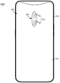
- FIG. 1 is a schematic front view of an electronic device according to some embodiments of the present application.
- FIG. 2 is a schematic rear view of an electronic device according to some embodiments of the present application.
- 3 to 6 are schematic diagrams of an arrangement manner of imaging devices in some embodiments of the present application.
- FIG. 7 is a schematic plan view of a lens and an imaging device according to some embodiments of the present application.
- FIG. 8 is a perspective structural diagram of a time-of-flight module according to some embodiments of the present application.
- FIG. 9 is a schematic top view of a time-of-flight module according to some embodiments of the present application.
- FIG. 10 is a schematic bottom view of a time-of-flight module according to some embodiments of the present application.
- FIG. 11 is a schematic side view of a time-of-flight module according to some embodiments of the present application.
- FIG. 12 is a schematic cross-sectional view of the time-of-flight module shown in FIG. 9 along the XII-XII line;
- FIG. 13 is an enlarged schematic view of the XIII part in the time-of-flight module shown in FIG. 12; FIG.
- FIG. 14 is a schematic front view of a time-of-flight module according to some embodiments of the present application when the flexible circuit board is not bent;
- 15 to 18 are schematic structural diagrams of a light emitter according to some embodiments of the present application.
- the imaging device 100 includes a time-of-flight module 20 and a dual-camera module 10.
- the time of flight module 20 includes a light transmitter 23 and a light receiver 24, and the dual camera module 10 includes two cameras 11 and 12.
- the center C1 of the light transmitter 23, the center C2 of the light receiver 24, and the center C3 of the dual camera module 10 are located on the same straight line.
- the center C1 of the light transmitter 23, the center C2 of the light receiver 24, and the center C4 or C5 of a camera 11 or 12 are located on the same straight line.
- the center C1 of the light transmitter 23, the center C2 of the light receiver 24, the center C3 of the dual camera module 10, and the centers C4 and C5 of the two cameras 11, 12 are located on the same straight line L1.
- the dual camera module 10 includes a main camera 11 and a sub camera 12, a center C1 of the light transmitter 23, a center C2 of the light receiver 24, and a center C4 of the main camera 11 on the same straight line L2; Or the center C1 of the light transmitter 23, the center C2 of the light receiver 24, and the center C5 of the sub camera 12 are located on the same straight line L3.
- the time-of-flight module 20 further includes a substrate assembly 21 and a pad 22.
- the substrate assembly 21 includes a substrate 211 and a flexible circuit board 212 connected to each other.
- the spacer 22 is disposed on the substrate 211.
- the light transmitter 23 is configured to emit an optical signal outward.
- the light transmitter 23 is disposed on the cushion block 22.
- the flexible circuit board 212 is bent and one end of the flexible circuit board 212 is connected to the substrate 211 and the other end is connected to the light emitter 23.
- the light receiver 24 is provided on a substrate 211.
- the light receiver 24 includes a housing 241 and an optical element 242 disposed on the housing 241.
- the housing 241 is integrally formed with the cushion block 22.
- the cushion block 22 includes a protruding portion 225 protruding from the side edge 2111 of the substrate 211, and the flexible circuit board 212 is bent around the protruding portion 225.
- the outer surface 2251 of the protrusion 225 is a smooth curved surface.
- a receiving cavity 223 is defined on a side where the cushion block 22 is combined with the substrate 211.
- the time-of-flight module 20 further includes an electronic component 25 disposed on the substrate 211, and the electronic component 25 is contained in the receiving cavity 223.
- the electronic device 1000 includes: a casing 200 and the imaging device 100 according to any one of the foregoing embodiments.
- the casing 200 is provided with a through-hole 201.
- the imaging device 100 is installed on the casing 200.
- the imaging device 100 and The light passing holes 201 are aligned.
- the electronic device 1000 further includes a light transmitting lens 500.
- the lens 500 is mounted on the cabinet 200.
- the lens 500 covers the light-passing hole 201.
- An area of the lens 500 corresponding to the time-of-flight module 20 is provided with an infrared transmitting ink 501.
- the infrared transmitting ink 501 is used to transmit only infrared light.
- the casing 200 includes a front surface 204 and a back surface 205 opposite to each other, and the light through hole 201 penetrates the front surface 204 or the back surface 205.
- the dual camera module 10 includes a wide-angle camera 11 and a telephoto camera 12, and the electronic device 1000 further includes a processor 600.
- the processor 600 is configured to obtain a current distance between the target object and the electronic device 1000 in real time. When the current distance is less than a preset distance threshold, the wide-angle camera 11 collects image information of the target object. When the current distance is greater than or equal to the distance threshold, the telephoto camera 12 collects image information of the target object.
- the dual camera module 10 includes a color camera 11 and a black and white camera 12.
- the electronic device 1000 further includes a processor 600, which is configured to obtain the ambient light brightness of the current environment in real time.
- the black and white camera 12 collects image information of the current environment.
- the color camera 11 collects image information of the current environment.
- an electronic device 1000 includes a casing 200 and an imaging device 100.
- the electronic device 1000 may be a mobile phone, a tablet computer, a game console, a smart watch, a headset device, a drone, etc.
- the embodiment of the present application is described using the electronic device 1000 as a mobile phone. It can be understood that the specific form of the electronic device 1000 is Not limited to mobile phones.
- the case 200 can be used as a mounting carrier for the functional elements of the electronic device 1000.
- the case 200 can provide protection for the functional elements from dust, water, and drop.
- the functional elements can be the display screen 300, the receiver 400, and the like.
- the cabinet 200 includes a front surface 204 and a back surface 205 opposite to each other.
- the display screen 300 may be disposed on the front surface 204.
- the housing 200 is provided with a light-through hole 201. After the light passes through the light-through hole 201, it can enter the external environment from the inside of the housing 200, and the light in the external environment can also pass through the light-through hole 201 and enter the housing 200.
- the cabinet 200 includes a main body 202 and a movable bracket 203.
- the movable bracket 203 can be moved relative to the main body 202 under the driving of a driving device.
- the movable bracket 203 can be relatively
- the main body 202 slides to slide into or out of the main body 202.
- Some functional elements such as the display 300
- other functional elements such as the imaging device 100 and the receiver 400
- the movement of the movable support 203 can drive the other functional elements Retracted into or extended from the main body 202.
- the light through hole 201 is opened on the movable bracket 203.
- the imaging device 100 is mounted on the casing 200, and the imaging device 100 is aligned with the light-passing hole 201.
- the imaging device 100 is mounted on a movable bracket 203.
- the user can trigger the movable bracket 203 to slide out from the main body 202 to drive the imaging device 100 from the main body. Extending from 202, when the imaging device 100 is not needed, the movable bracket 203 can be triggered to slide into the main body 202 to drive the imaging device 100 to retract into the main body 202.
- FIG. 1 is only an example of a specific form of the cabinet 200 and cannot be understood as a limitation on the cabinet 200 of the present application.
- the light hole 201 may be fixed, and the imaging device 100 is fixedly disposed and aligned with the light passing hole 201. In another example, the imaging device 100 is fixedly disposed below the display screen 300.
- the imaging device 100 includes a time-of-flight module 20 and a dual-camera module 10.
- the time of flight module 20 includes a light transmitter 23 and a light receiver 24, and the dual camera module 10 includes two cameras 11 and 12.
- the center C1 of the light transmitter 23, the center C2 of the light receiver 24, and the center C3 of the dual camera module 10 are located on the same straight line (as shown in Figs. 3 and 4).
- the center C1 of the light transmitter 23, the center C2 of the light receiver 24, and the center C4 or C5 of a camera 11 or 12 are located on the same straight line (as shown in Figs. 5 and 6).
- the time-of-flight module 20 can obtain the depth information of the measured object through the principle of time-of-flight, and then combine it with the image information of the measured object obtained by the dual-camera module 10.
- the time-of-flight module 20 acquires depth information through the principle of time of flight, the depth information obtained for a distanced or small-sized object is still highly accurate.
- the center C1 of the light transmitter 23, the center C2 of the light receiver 24, and the center C3 of the dual camera module 10 are located on the same straight line; or the center C1 of the light transmitter 23 and the center C2 of the light receiver 24, And the center C4 or C5 of one camera 11 or 12 is located on the same straight line; the overall arrangement of the imaging device 100 is beautiful and the structure is compact.
- the center C1 of the light transmitter 23, the center C2 of the light receiver 24, the center C3 of the dual camera module 10, and the center C4 of the two cameras 11 and 12. C5 is on the same straight line L1.
- the light transmitter 23, the light receiver 24, and the two cameras 11, 12 are arranged along the extending direction of the straight line L1, and the width of the imaging device 100 in the direction perpendicular to the straight line L1 is small, which facilitates the installation of the imaging device 1000 Inside the case 200.
- the imaging device 1000 may be installed in the casing 200 such that the straight line L1 is parallel to the bottom wall 206 of the casing 200 (as shown in FIG. 1), or the straight line L1 is parallel to the side wall 207 of the casing 200 (such as figure 2).
- the arrangement of the imaging device 100 may also be the center C1 of the light transmitter 23, the center C2 of the light receiver 24, and the center C3 of the dual camera module 10 on the same straight line, and the straight line It does not pass through the centers C4, C5 of the two cameras 11, 12 at this time, the line may be perpendicular to the line connecting the centers C4, C5 of the two cameras 11, 12 or at an acute angle to make the center of the light receiver 24
- the line connecting C2 and the centers C4 and C5 of the two cameras 11 and 12 can form a triangle.
- the dual camera module 10 includes a main camera 11 and a sub camera 12.
- the center C1 of the light transmitter 23, the center C2 of the light receiver 24, and the center C4 of the main camera 11 are located.
- the connection line between the center C4 of the main camera 11 and the center C5 of the sub camera 12 may be perpendicular to the straight line L2.
- the center C1 of the light transmitter 23, the center C2 of the light receiver 24, and the center C5 of the sub camera 12 are located on the same straight line L3 (as shown in FIG. 6).
- the connection line between the center C4 of the main camera 11 and the center C5 of the sub camera 12 may be perpendicular to the straight line L3.
- the straight line L2 or the straight line L3 may be parallel to the bottom wall 206 of the cabinet 200, or may be parallel to the side wall 207 of the cabinet 200.
- the center refers to the front view when the imaging device 100 is mounted on the casing 200 (front view in the direction in which the front surface 204 points to the back surface 205 or in the direction in which the back surface 205 points to the front surface 204).
- the center C1 of the light receiver 24 is the geometric center of the light receiver 24 when the imaging device 100 is viewed from the front.
- the light through hole 201 penetrates the front side 204 of the casing 200.
- the optical signal emitted by the light transmitter 23 can pass through the front face 204 of the electronic device 1000 to be transmitted to the outside, and the dual camera module 10 can be used as a front camera of the electronic device 1000.
- the depth information obtained by the time-of-flight module 20 can be used for functions such as ranging, unlocking, and payment, and the image information obtained by the dual-camera module 10 can be used for functions such as selfies.
- the through-hole 201 passes through the back surface 205 of the casing 200.
- the optical signal emitted by the light transmitter 23 can pass through the back surface 205 of the electronic device 1000 to be transmitted to the outside, and the dual camera module 10 can be used as a rear camera of the electronic device 1000.
- the depth information obtained by the time-of-flight module 20 can be used for functions such as ranging and modeling, and the image information obtained by the dual-camera module 10 can be used for functions such as shooting scenes.
- the electronic device 1000 further includes a light transmitting lens 500.
- the lens 500 is mounted on the cabinet 200.
- the lens 500 covers the light-passing hole 201.
- An area (such as the shaded area in FIG. 7) corresponding to the time-of-flight module 20 on the lens 500 is provided with an infrared transmitting ink 501.
- the infrared transmitting ink 501 is used to transmit only infrared light.
- the infrared transmissive ink 501 has a high transmittance to infrared light, for example, the transmittance can reach 85% or more, while the transmittance to light other than infrared light is low or makes light other than infrared light Impervious at all.
- infrared light can pass through the infrared transmission ink 501, and light other than infrared light (such as visible light) can hardly pass through the infrared transmission
- the ink 501 therefore, it is difficult for a user to see the time-of-flight module 20 inside the casing 200 through the light-through hole 201, and the appearance of the electronic device 1000 is more beautiful.
- the dual camera module 10 includes a wide-angle camera 11 and a telephoto camera 12 (the wide-angle camera 11 and the telephoto camera 12 can serve as the main camera 11 and the sub-camera 12),
- the electronic device 1000 further includes a processor 600.
- the processor 600 is configured to obtain a current distance between the target object and the electronic device 1000 in real time. When the current distance is less than a preset distance threshold, the wide-angle camera 11 collects image information of the target object. When the current distance is greater than or equal to the distance threshold, the telephoto camera 12 collects image information of the target object.
- wide-angle and telephoto are relative terms.
- the wide-angle camera 11 has a larger field of view relative to the telephoto camera 12, and the telephoto camera 11 has a longer focal distance and a longer shooting distance than the wide-angle camera 12.
- the electronic device 1000 can switch the camera used to collect image information in real time according to the current distance.
- the processor 600 obtains the current distance between the target object and the electronic device 1000 as d1, where d1 ⁇ d0.
- the wide-angle camera 11 collects image information of the target object, and the image information is a wide-angle image at this time.
- the processor 600 may construct a three-dimensional image of the target object according to the depth information and the wide-angle image.
- the processor 600 obtains a current distance between the target object and the electronic device 1000 as d2, where d2> d0.
- the focus camera 12 collects image information of the target object again. At this time, the image information is a telephoto image.
- the processor 600 may construct a three-dimensional image of the target object based on the depth information and the telephoto image.
- the electronic device 1000 includes a wide-angle camera 11 and a telephoto camera 12 at the same time.
- the processor 600 can switch the wide-angle camera 11 or the telephoto camera 12 according to the actual situation to collect image information of the target object, thereby constructing two types of three-dimensional, wide-angle and telephoto Images, which will help improve the photo experience.
- the processor 600 may obtain depth information collected by the time-of-flight module 20.
- the current distance acquired by the processor 600 may also be acquired by the time-of-flight module 20 or other functional modules, such as the current distance acquired by a structured light module or a proximity sensor.
- the dual camera module 10 includes a color camera (ie, an RGB camera) 11 and a black and white camera (ie, a Mono camera) 12 (the color camera 11 and the black and white camera 12 can be used as the main camera 11 and the sub camera 12) .
- the electronic device 1000 further includes a processor 600, which is configured to obtain the ambient light brightness of the current environment in real time. When the ambient light brightness is less than a preset brightness threshold, the black and white camera 12 collects image information of the current environment. When the ambient light brightness is greater than or equal to the brightness threshold, the color camera 11 collects image information of the current environment.
- the black and white camera 12 can improve the shooting quality of low-light / night scene images. Therefore, when the ambient light brightness is less than the brightness threshold, image information can be collected by the black and white camera 12. When the ambient light brightness is greater than or equal to the brightness threshold, image information may be collected by the color camera 11. Assume that the brightness threshold is Q0. At the first moment, the ambient light brightness obtained by the processor 600 is Q1, where Q1 ⁇ Q0. At this time, the black and white camera 12 collects image information of the current environment. This image information is a Mono image. The processor 600 can construct a three-dimensional image of the current environment according to the depth information and the Mono image.
- the ambient light brightness obtained by the processor 600 is Q2, where Q2> Q0.
- the color camera 11 collects an image of the current environment again.
- Information this image information is an RGB image
- the processor 600 may construct a three-dimensional image of the current environment according to the depth information and the RGB image.
- the electronic device 1000 includes both a color camera 11 and a black-and-white camera 12.
- the processor 600 can switch the color camera 11 or the black-and-white camera 12 according to the actual situation to collect image information of the current environment, thereby constructing two different types of three-dimensional images, RGB and Mono. Conducive to improving the photo experience.
- the time-of-flight module 20 includes a substrate assembly 21, a spacer 22, a light transmitter 23 and a light receiver 24.
- the substrate assembly 21 includes a substrate 211 and a flexible circuit board 212 connected to each other.
- the spacer 22 is disposed on the substrate 211.
- the light transmitter 23 is configured to emit an optical signal outward.
- the light transmitter 23 is disposed on the cushion block 22.
- the flexible circuit board 212 is bent and one end of the flexible circuit board 212 is connected to the substrate 211 and the other end is connected to the light emitter 23.
- the light receiver 24 is disposed on the substrate 211.
- the light receiver 24 is used to receive the light signal emitted by the reflected light transmitter 23.
- the light receiver 24 includes a housing 241 and an optical element 242 disposed on the housing 241.
- the housing 241 is integrally connected with the cushion block 22.
- the substrate assembly 21 includes a substrate 211 and a flexible circuit board 212.
- the substrate 211 may be a printed circuit board or a flexible circuit board, and the control circuit of the time-of-flight module 20 may be laid on the substrate 211.
- One end of the flexible circuit board 212 can be connected to the substrate 211, and the flexible circuit board 212 can be bent at a certain angle, so that the relative positions of the devices connected at both ends of the flexible circuit board 212 can be selected.
- the pad 22 is disposed on the substrate 211.
- the spacer 22 is in contact with the substrate 211 and is carried on the substrate 211.
- the spacer 22 may be combined with the substrate 211 by means of adhesion or the like.
- the material of the spacer 22 may be metal, plastic, or the like.
- a surface where the pad 22 is combined with the substrate 211 may be a flat surface, and a surface opposite to the combined surface of the pad 22 may also be a flat surface, so that the light emitter 23 has a comparatively high quality when it is disposed on the pad 22. Good smoothness.
- the light transmitter 23 is configured to emit an optical signal outwards.
- the light signal may be infrared light, and the light signal may be a lattice spot emitted to the object to be measured.
- the light signal is emitted from the light transmitter 23 at a certain divergence angle. .
- the light transmitter 23 is disposed on the spacer 22. In the embodiment of the present application, the light transmitter 23 is disposed on the side of the spacer 22 opposite to the substrate 211, or the spacer 22 includes the substrate 211 and the light transmitter. 23 are spaced apart so that a height difference is formed between the light emitter 23 and the substrate 211.
- the light transmitter 23 is also connected to the flexible circuit board 212, and the flexible circuit board 212 is bent.
- One end of the flexible circuit board 212 is connected to the substrate 211, and the other end is connected to the light transmitter 23, so as to transfer the control signal of the light transmitter 23 from the substrate 211.
- the signal is transmitted to the optical transmitter 23, or a feedback signal of the optical transmitter 23 (for example, time information, frequency information of the optical signal transmitted by the optical transmitter 23, temperature information of the optical transmitter 23, etc.) is transmitted to the substrate 211.
- the light receiver 24 is used for receiving an optical signal emitted by the reflected light transmitter 23.
- the light receiver 24 is disposed on the substrate 211, and the contact surface of the light receiver 24 and the substrate 211 is substantially flush with the contact surface of the pad 22 and the substrate 211 (that is, the installation starting points of the two are on the same plane).
- the light receiver 24 includes a housing 241 and an optical element 242.
- the casing 241 is disposed on the substrate 211, and the optical element 242 is disposed on the casing 241.
- the casing 241 may be a lens holder and a lens barrel of the light receiver 24, and the optical element 242 may be a lens or other elements disposed in the casing 241. .
- the light receiver 24 may further include a photosensitive chip (not shown).
- the optical signal reflected by the measured object is irradiated into the photosensitive chip through the optical element 242, and the photosensitive chip responds to the optical signal.
- the time-of-flight module 20 calculates the time difference between the light signal emitted by the light transmitter 23 and the light sensor receiving the light signal reflected by the measured object, and further obtains the depth information of the measured object, which can be used for distance measurement, For generating depth images or for 3D modeling.
- the housing 241 and the cushion block 22 are integrally connected. Specifically, the housing 241 and the spacer 22 may be integrally formed.
- the materials of the housing 241 and the spacer 22 are the same and are integrally formed by injection molding, cutting or the like; or the materials of the housing 241 and the spacer 22 are different, both Integrated molding by two-color injection molding.
- the housing 241 and the spacer 22 may also be separately formed, and the two form a matching structure.
- the housing 241 and the spacer 22 may be first integrated into one body, and then jointly disposed on the substrate 211; Alternatively, one of the housing 241 and the pad 22 may be disposed on the substrate 211, and then the other may be disposed on the substrate 211 and connected together.
- the pad 22 can raise the height of the light emitter 23, thereby increasing the height of the light emitting surface of the light emitter 23, and the light emitter 23
- the emitted light signal is not easily blocked by the light receiver 24, so that the light signal can be completely irradiated on the measured object.
- the exit surface of the light transmitter 23 may be flush with the entrance surface of the light receiver 24, or the exit surface of the light transmitter 23 may be slightly lower than the entrance surface of the light receiver 24, or it may be the exit surface of the light transmitter 23 Slightly higher than the incident surface of the light receiver 24.
- the substrate assembly 21 further includes a reinforcing plate 213.
- the reinforcing plate 213 is coupled to a side of the substrate 211 opposite to the pad 22.
- the reinforcing plate 213 may cover one side of the substrate 211, and the reinforcing plate 213 may be used to increase the strength of the substrate 211 and prevent deformation of the substrate 211.
- the reinforcing plate 213 may be made of a conductive material, such as a metal or an alloy.
- the reinforcing plate 213 and the casing 200 may be electrically connected to make the reinforcing plate 213. Grounding and effectively reducing the interference of static electricity from external components on the time of flight module 20.
- the cushion block 22 includes a protruding portion 225 protruding from the side edge 2111 of the substrate 211, and the flexible circuit board 212 is bent around the protruding portion 225. Specifically, a part of the cushion block 22 is directly carried on the substrate 211, and another part is not in direct contact with the substrate 211, and protrudes from the side edge 2111 of the substrate 211 to form a protruding portion 225.
- the flexible circuit board 212 may be connected to the side edge 2111, and the flexible circuit board 212 is bent around the protrusion 225, or the flexible circuit board 212 is bent so that the protrusion 225 is located in a space surrounded by the flexible circuit board 212. Inside, when the flexible circuit board 212 is subjected to an external force, the flexible circuit board 212 will not collapse inward and cause excessive bending, which will cause damage to the flexible circuit board 212.
- the outer surface 2251 of the protruding portion 225 is a smooth curved surface (for example, the outer surface of a cylinder, etc.), that is, the outer surface 2251 of the protruding portion 225 does not form a curvature. Hence, even if the flexible circuit board 212 is bent over the outer side 2251 of the protruding portion 225, the degree of bending of the flexible circuit board 212 will not be too large, which further ensures the integrity of the flexible circuit board 212.
- the time-of-flight module 20 further includes a connector 26 connected to the substrate 211.
- the connector 26 is used to connect the substrate assembly 21 and an external device.
- the connector 26 and the flexible circuit board 212 are respectively connected to opposite ends of the substrate 211.
- the connector 26 may be a connection socket or a connector.
- the connector 26 may be connected to the main board of the electronic device 1000 so that the time-of-flight module 20 is electrically connected to the main board.
- the connector 26 and the flexible circuit board 212 are respectively connected to opposite ends of the substrate 211.
- the connectors 26 and the flexible circuit board 212 may be respectively connected to the left and right ends of the substrate 211, or respectively connected to the front and rear ends of the substrate 211.
- the light transmitter 23 and the light receiver 24 are arranged along a straight line L, and the connector 26 and the flexible circuit board 212 are located on opposite sides of the straight line L, respectively. It can be understood that, since the light transmitter 23 and the light receiver 24 are arranged in an array, the size of the time-of-flight module 20 may be larger in the direction of the straight line L.
- the connector 26 and the flexible circuit board 212 are respectively disposed on opposite sides of the straight line L, which will not increase the size of the time-of-flight module 20 in the direction of the straight line L, thereby facilitating the installation of the time-of-flight module 20 on the electronic device 1000.
- On the chassis 200 On the chassis 200.
- a receiving cavity 223 is defined on a side where the cushion block 22 is combined with the substrate 211.
- the time-of-flight module 20 further includes an electronic component 25 disposed on the substrate 211, and the electronic component 25 is contained in the receiving cavity 223.
- the electronic component 25 may be a capacitor, an inductor, a transistor, a resistor, or the like.
- the electronic component 25 may be electrically connected to a control line laid on the substrate 211 and used to drive or control the operation of the light transmitter 23 or the light receiver 24.
- the electronic component 25 is contained in the containing cavity 223, and the space in the cushion block 22 is used reasonably.
- the number of the receiving cavities 223 may be one or more, and the plurality of receiving cavities 223 may be spaced apart from each other.
- the positions of the receiving cavity 223 and the electronic component 25 may be aligned and the pad 22 may be disposed at On the substrate 211.
- the cushion block 22 is provided with an avoiding through hole 224 communicating with at least one receiving cavity 223, and at least one electronic component 25 extends into the avoiding through hole 224.
- the height of the electronic component 25 is required to be not higher than the height of the containing cavity 223.
- an avoiding through hole 224 corresponding to the receiving cavity 223 may be provided, and the electronic component 25 may partially extend into the avoiding through hole 224, so as not to increase the height of the spacer 22
- the electronic component 25 is arranged.
- the light emitter 23 includes an emission substrate assembly 231, a light source assembly 232, and a housing 233.
- the emission substrate assembly 231 is disposed on the pad 22, and the emission substrate assembly 231 is connected to the flexible circuit board 212.
- the light source assembly 232 is disposed on the emission substrate assembly 231, and the light source assembly 232 is configured to emit an optical signal.
- the casing 233 is disposed on the emission substrate assembly 231.
- the casing 233 is formed with a receiving space 2331.
- the receiving space 2331 can be used for receiving the light source module 232.
- the flexible circuit board 212 may be detachably connected to the transmitting substrate assembly 231.
- the light source assembly 232 is electrically connected to the emission substrate assembly 231.
- the housing 233 may be bowl-shaped as a whole, and the opening of the housing 233 is downwardly covered on the emitting substrate assembly 231 to receive the light source assembly 232 in the receiving space 2331.
- a light outlet 2332 corresponding to the light source component 232 is provided on the housing 233.
- the optical signal emitted from the light source component 232 passes through the light outlet 2332 and is emitted.
- the light signal can pass directly through the light outlet 2332. It can also pass through the optical outlet 2332 after changing the optical path through other optical devices.
- the emitting substrate assembly 231 includes a emitting substrate 2311 and a reinforcing member 2312.
- the emission substrate 2311 is connected to a flexible circuit board 212.
- the light source assembly 232 and the reinforcing member 2312 are disposed on opposite sides of the emission substrate 2311.
- the specific type of the transmitting substrate 2311 may be a printed circuit board or a flexible circuit board, and a control circuit may be laid on the transmitting substrate 2311.
- the reinforcing member 2312 may be fixedly connected to the emitting substrate 2311 by means of gluing, riveting, or the like.
- the reinforcing member 2312 may increase the overall strength of the emitting substrate assembly 231.
- the reinforcing member 2312 can directly contact the pad 22, the emission substrate 2311 is not exposed to the outside, and does not need to be in direct contact with the pad 22, and the emission substrate 2311 is not susceptible to dust, etc. Pollution.
- the reinforcing member 2312 and the cushion block 22 are formed separately.
- the spacer 22 may be first mounted on the substrate 211.
- two ends of the flexible circuit board 212 are respectively connected to the substrate 211 and the emitting substrate 2311, and the flexible circuit board 212 may not be bent first ( (As shown in Figure 14).
- the flexible circuit board 212 is then bent, so that the reinforcing member 2312 is disposed on the cushion block 22.
- the reinforcing member 2312 and the spacer 22 may be integrally formed, for example, integrally formed by a process such as injection molding.
- the spacer 22 and the light emitter 23 may be installed together.
- the substrate 211 On the substrate 211.
- a first positioning member 2313 is formed on the reinforcing member 2312.
- the cushion block 22 includes a body 221 and a second positioning member 222.
- the second positioning member 222 is formed on the body 221.
- the first positioning member 2313 cooperates with the second positioning member 222.
- the relative movement between the emitting substrate assembly 231 and the pad 22 can be effectively restricted.
- the specific types of the first positioning member 2313 and the second positioning member 222 can be selected according to needs.
- the first positioning member 2313 is a positioning hole formed in the reinforcing member 2312
- the second positioning member 222 is a positioning column. Protrude into the positioning hole so that the first positioning member 2313 and the second positioning member 222 cooperate with each other; or the first positioning member 2313 is a positioning column formed on the reinforcing member 2312, and the second positioning member 222 is a positioning hole and the positioning column Project into the positioning hole so that the first positioning member 2313 and the second positioning member 222 cooperate with each other; or the number of the first positioning member 2313 and the second positioning member 222 are multiple, and part of the first positioning member 2313 is a positioning hole, Part of the second positioning member 222 is a positioning column, part of the first positioning member 2313 is a positioning column, and part of the second positioning member 222 is a positioning hole.
- the positioning column projects into the positioning hole so that the first positioning member 2313 and the second positioning member 222 work cooperatively.
- the structure of the light source component 232 will be described as an example below:
- the light source assembly 232 includes a light source 60, a lens barrel 70, a diffuser 80 and a protective cover 90.
- the light source 60 is connected to the emitting substrate assembly 231.
- the lens barrel 70 includes a first surface 71 and a second surface 72 opposite to each other.
- the lens barrel 11 defines a storage cavity 75 that penetrates the first surface 71 and the second surface 72.
- the first surface 71 The second surface 72 is recessed to form a mounting groove 76 communicating with the storage cavity 75.
- the diffuser 80 is installed in the mounting groove 76.
- the protective cover 90 is mounted on the side where the first surface 71 of the lens barrel 70 is located, and the diffuser 80 is sandwiched between the protective cover 90 and the bottom surface 77 of the mounting groove 76.
- the protective cover 90 can be mounted on the lens barrel 70 by means of screw connection, engagement, and fastener connection.
- the protective cover 90 when the protective cover 90 includes a top wall 91 and a protective side wall 92, the protective cover 90 (protective side wall 92) is provided with internal threads and the lens barrel 70 is provided with external threads.
- the protective cover The internal thread of 90 is screwed with the external thread of the lens barrel 70 to mount the protective cover 90 on the lens barrel 70; or, referring to FIG. 16, when the protective cover 90 includes a top wall 91, the protective cover 90 (top wall 91) A locking hole 95 is opened, and a hook 73 is provided at an end of the lens barrel 70.
- the hook 73 is inserted into the locking hole 95 so that the protective cover 90 is mounted on the lens barrel 70. 17; when the protective cover 90 includes a top wall 91 and a protective side wall 92, the protective cover 90 (protective side wall 92) is provided with a locking hole 95, and a hook 73 is provided on the lens barrel 70.
- the hook 73 is inserted into the hole 95 to mount the protective cover 90 on the lens barrel 70; or, referring to FIG.
- the protective cover 90 when the protective cover 90 includes the top wall 91, The end of the lens barrel 70 is provided with a first positioning hole 74, the protective cover 90 (top wall 91) is provided with a second positioning hole 93 corresponding to the first positioning hole 74, and the fastener 94 passes through the second positioning hole 93 And locked A first positioning hole 74 to the protective cover 90 is mounted on the lens barrel 70.
- the protective cover 90 is mounted on the lens barrel 70, the protective cover 90 is in contact with the diffuser 80 and the diffuser 80 is in contact with the bottom surface 77, so that the diffuser 80 is sandwiched between the protective cover 90 and the bottom surface 77.
- the light source assembly 232 is provided with a mounting groove 76 on the lens barrel 70 and the diffuser 80 is installed in the mounting groove 76, and is mounted on the lens barrel 70 through a protective cover 90 to clamp the diffuser 80 between the protective cover 90 and the installation. Between the bottom surfaces 77 of the grooves 76, the diffuser 80 is actually fixed to the lens barrel 70. And avoid using glue to fix the diffuser 80 on the lens barrel 70, so as to prevent the glue from diffusing and solidifying on the surface of the diffuser 80 and affecting the microstructure of the diffuser 80 after the glue is volatilized to a gaseous state, and can prevent connection and diffusion When the glue of the lens holder 70 and the lens barrel 70 decreases due to aging, the diffuser 80 falls off from the lens barrel 70.
- first and second are used for descriptive purposes only, and cannot be understood as indicating or implying relative importance or implicitly indicating the number of technical features indicated.
- the features defined as “first” and “second” may explicitly or implicitly include at least one of the features.
- the meaning of “plurality” is at least two, for example, two, three, unless specifically defined otherwise.
Abstract
L'invention concerne un dispositif d'imagerie (100), comprenant un module de temps de vol (20) et un module de caméra double (10). Le module de temps de vol (20) comprend un émetteur de lumière (23) et un récepteur de lumière (24). Le module à double caméra (10) comprend deux caméras (11, 12). Le centre de l'émetteur de lumière (23), le centre du récepteur de lumière (24) et le centre du module à deux caméras (10) sont situés sur la même ligne droite; ou le centre de l'émetteur de lumière (23), le centre du récepteur de lumière (24) et le centre d'une caméra du module à deux caméras (10) sont situés sur la même ligne droite.
Applications Claiming Priority (2)
| Application Number | Priority Date | Filing Date | Title |
|---|---|---|---|
| CN201810962517.7 | 2018-08-22 | ||
| CN201810962517.7A CN109040556A (zh) | 2018-08-22 | 2018-08-22 | 成像装置及电子设备 |
Publications (1)
| Publication Number | Publication Date |
|---|---|
| WO2020038068A1 true WO2020038068A1 (fr) | 2020-02-27 |
Family
ID=64627971
Family Applications (1)
| Application Number | Title | Priority Date | Filing Date |
|---|---|---|---|
| PCT/CN2019/090083 WO2020038068A1 (fr) | 2018-08-22 | 2019-06-05 | Dispositif d'imagerie et appareil électronique |
Country Status (2)
| Country | Link |
|---|---|
| CN (1) | CN109040556A (fr) |
| WO (1) | WO2020038068A1 (fr) |
Cited By (2)
| Publication number | Priority date | Publication date | Assignee | Title |
|---|---|---|---|---|
| CN114257724A (zh) * | 2021-11-08 | 2022-03-29 | 厦门聚视智创科技有限公司 | 一种手机背板飞拍控制方法及其系统 |
| CN115550482A (zh) * | 2022-02-28 | 2022-12-30 | 荣耀终端有限公司 | 电子设备 |
Families Citing this family (10)
| Publication number | Priority date | Publication date | Assignee | Title |
|---|---|---|---|---|
| CN109005348A (zh) * | 2018-08-22 | 2018-12-14 | Oppo广东移动通信有限公司 | 电子装置和电子装置的控制方法 |
| CN109040556A (zh) * | 2018-08-22 | 2018-12-18 | Oppo广东移动通信有限公司 | 成像装置及电子设备 |
| CN112492138A (zh) * | 2018-12-24 | 2021-03-12 | 华为技术有限公司 | 摄像组件及电子设备 |
| CN109639983B (zh) * | 2019-01-03 | 2020-09-04 | Oppo广东移动通信有限公司 | 拍照方法、装置、终端及计算机可读存储介质 |
| CN111741283A (zh) * | 2019-03-25 | 2020-10-02 | 华为技术有限公司 | 图像处理的装置和方法 |
| EP3930321A4 (fr) * | 2019-03-25 | 2022-04-20 | Huawei Technologies Co., Ltd. | Procédé de flou à grande ouverture à base de caméra double + tof |
| JP6805448B2 (ja) * | 2019-04-23 | 2020-12-23 | エスゼット ディージェイアイ テクノロジー カンパニー リミテッドSz Dji Technology Co.,Ltd | 制御装置、撮像システム、移動体、制御方法、及びプログラム |
| CN209823807U (zh) * | 2019-07-09 | 2019-12-20 | Oppo广东移动通信有限公司 | 电子设备 |
| CN111024626B (zh) * | 2019-12-24 | 2022-12-13 | Oppo广东移动通信有限公司 | 光源模组、成像装置和电子设备 |
| CN117321381A (zh) * | 2021-10-26 | 2023-12-29 | 京东方科技集团股份有限公司 | 飞行时间相机模组及显示设备 |
Citations (5)
| Publication number | Priority date | Publication date | Assignee | Title |
|---|---|---|---|---|
| US6326994B1 (en) * | 1997-01-22 | 2001-12-04 | Sony Corporation | Matched field-of-view stereographic imaging apparatus |
| CN107277339A (zh) * | 2017-08-10 | 2017-10-20 | 信利光电股份有限公司 | 电子设备和摄像模组 |
| CN107493411A (zh) * | 2017-08-09 | 2017-12-19 | 广东欧珀移动通信有限公司 | 图像处理系统及方法 |
| CN108337414A (zh) * | 2018-02-28 | 2018-07-27 | 信利光电股份有限公司 | 一种用于获取景深信息的摄像设备以及电子设备 |
| CN109040556A (zh) * | 2018-08-22 | 2018-12-18 | Oppo广东移动通信有限公司 | 成像装置及电子设备 |
Family Cites Families (7)
| Publication number | Priority date | Publication date | Assignee | Title |
|---|---|---|---|---|
| CN102736199B (zh) * | 2012-05-23 | 2014-10-22 | 日月光半导体制造股份有限公司 | 光耦合模块构造 |
| CN106254744A (zh) * | 2016-09-23 | 2016-12-21 | 成都创慧科达科技有限公司 | 一种移动终端的外置双摄像头 |
| CN106657455B (zh) * | 2016-10-25 | 2023-05-05 | 奥比中光科技集团股份有限公司 | 一种带可旋转摄像头的电子设备 |
| CN106341611A (zh) * | 2016-11-29 | 2017-01-18 | 广东欧珀移动通信有限公司 | 控制方法、控制装置及电子装置 |
| CN107390853B (zh) * | 2017-06-26 | 2020-11-06 | Oppo广东移动通信有限公司 | 电子装置 |
| CN108089199A (zh) * | 2017-12-26 | 2018-05-29 | 深圳慎始科技有限公司 | 一种半固态三维彩色成像装置 |
| CN108259724A (zh) * | 2018-03-13 | 2018-07-06 | 欧菲影像技术(广州)有限公司 | 摄像模组及其支架结构 |
-
2018
- 2018-08-22 CN CN201810962517.7A patent/CN109040556A/zh active Pending
-
2019
- 2019-06-05 WO PCT/CN2019/090083 patent/WO2020038068A1/fr active Application Filing
Patent Citations (5)
| Publication number | Priority date | Publication date | Assignee | Title |
|---|---|---|---|---|
| US6326994B1 (en) * | 1997-01-22 | 2001-12-04 | Sony Corporation | Matched field-of-view stereographic imaging apparatus |
| CN107493411A (zh) * | 2017-08-09 | 2017-12-19 | 广东欧珀移动通信有限公司 | 图像处理系统及方法 |
| CN107277339A (zh) * | 2017-08-10 | 2017-10-20 | 信利光电股份有限公司 | 电子设备和摄像模组 |
| CN108337414A (zh) * | 2018-02-28 | 2018-07-27 | 信利光电股份有限公司 | 一种用于获取景深信息的摄像设备以及电子设备 |
| CN109040556A (zh) * | 2018-08-22 | 2018-12-18 | Oppo广东移动通信有限公司 | 成像装置及电子设备 |
Cited By (4)
| Publication number | Priority date | Publication date | Assignee | Title |
|---|---|---|---|---|
| CN114257724A (zh) * | 2021-11-08 | 2022-03-29 | 厦门聚视智创科技有限公司 | 一种手机背板飞拍控制方法及其系统 |
| CN114257724B (zh) * | 2021-11-08 | 2023-11-21 | 厦门聚视智创科技有限公司 | 一种手机背板飞拍控制方法及其系统 |
| CN115550482A (zh) * | 2022-02-28 | 2022-12-30 | 荣耀终端有限公司 | 电子设备 |
| CN115550482B (zh) * | 2022-02-28 | 2023-06-13 | 荣耀终端有限公司 | 电子设备 |
Also Published As
| Publication number | Publication date |
|---|---|
| CN109040556A (zh) | 2018-12-18 |
Similar Documents
| Publication | Publication Date | Title |
|---|---|---|
| WO2020038068A1 (fr) | Dispositif d'imagerie et appareil électronique | |
| WO2020038054A1 (fr) | Ddispositif électronique et procédé de commande associé | |
| WO2020125388A1 (fr) | Module à temps de vol et dispositif électronique | |
| WO2020038063A1 (fr) | Dispositif électronique et procédé de commande pour dispositif électronique | |
| WO2020134879A1 (fr) | Ensemble caméra et dispositif électronique | |
| WO2020038060A1 (fr) | Module de projection laser et son procédé de commande, et dispositif d'acquisition d'images et appareil électronique | |
| WO2020052289A1 (fr) | Module d'acquisition de profondeur et appareil électronique | |
| CN108873221A (zh) | 激光投射装置、tof深度相机和电子设备 | |
| US11741746B2 (en) | Electronic device | |
| EP3575865B1 (fr) | Ensemble électronique et dispositif électronique | |
| WO2020052288A1 (fr) | Module de collecte de profondeur et terminal mobile | |
| WO2020038056A1 (fr) | Ensemble temps de vol et dispositif électronique | |
| KR102350059B1 (ko) | 광학 기기 | |
| EP3609168B1 (fr) | Support, ensemble d'entrée/sortie et terminal | |
| WO2020038057A1 (fr) | Module de collecte de profondeur et dispositif électronique | |
| WO2020038055A1 (fr) | Composant de temps de vol et terminal mobile | |
| WO2020038052A1 (fr) | Ensemble d'entrée/sortie et dispositif mobile | |
| WO2021027580A1 (fr) | Terminal | |
| WO2020253686A1 (fr) | Module de projection laser, caméra de profondeur et dispositif électronique | |
| CN210694195U (zh) | 一种集成3d成像装置及电子设备 | |
| CN113691705A (zh) | 摄像模组及电子设备 | |
| CN111107206A (zh) | 电子设备 | |
| CN213693886U (zh) | 一种摄像头模组及设备 | |
| CN216930133U (zh) | 一种小型化的用于人脸识别的tof模组 | |
| WO2020037996A1 (fr) | Module d'obtention de profondeur et dispositif électronique |
Legal Events
| Date | Code | Title | Description |
|---|---|---|---|
| 121 | Ep: the epo has been informed by wipo that ep was designated in this application |
Ref document number: 19852737 Country of ref document: EP Kind code of ref document: A1 |
|
| NENP | Non-entry into the national phase |
Ref country code: DE |
|
| 122 | Ep: pct application non-entry in european phase |
Ref document number: 19852737 Country of ref document: EP Kind code of ref document: A1 |