WO2020022295A1 - 光学素子、光学系、および光学装置 - Google Patents
光学素子、光学系、および光学装置 Download PDFInfo
- Publication number
- WO2020022295A1 WO2020022295A1 PCT/JP2019/028727 JP2019028727W WO2020022295A1 WO 2020022295 A1 WO2020022295 A1 WO 2020022295A1 JP 2019028727 W JP2019028727 W JP 2019028727W WO 2020022295 A1 WO2020022295 A1 WO 2020022295A1
- Authority
- WO
- WIPO (PCT)
- Prior art keywords
- optical element
- light
- absorbing layer
- flange portion
- light absorbing
- Prior art date
- Legal status (The legal status is an assumption and is not a legal conclusion. Google has not performed a legal analysis and makes no representation as to the accuracy of the status listed.)
- Ceased
Links
Images


Classifications
-
- G—PHYSICS
- G02—OPTICS
- G02B—OPTICAL ELEMENTS, SYSTEMS OR APPARATUS
- G02B5/00—Optical elements other than lenses
-
- G—PHYSICS
- G02—OPTICS
- G02B—OPTICAL ELEMENTS, SYSTEMS OR APPARATUS
- G02B7/00—Mountings, adjusting means, or light-tight connections, for optical elements
- G02B7/02—Mountings, adjusting means, or light-tight connections, for optical elements for lenses
Definitions
- the present invention relates to an optical element capable of reducing stray light, an optical system having the optical element, and an optical device having the optical element.
- stray light may be generated due to reflection inside the lens or an imaging system including the lens. Then, so-called ghosts and flares may occur due to stray light.
- Patent Literature 1 also discloses a method in which a peripheral portion of a lens is roughened and light is scattered by the roughened portion.
- an object of one embodiment of the present invention to provide an optical element capable of reducing stray light without significantly impairing the accuracy of a flange surface, an optical system having the optical element, and an optical device having the optical element.
- An optical element is an optical element including a curved surface and a flange portion having an annular flat portion extending in the outer radial direction from the curved surface, and at least a part of the flange portion includes an optical element.
- a light absorbing layer for reducing the reflectance when light enters from the inside is provided, and the thickness of the light absorbing layer is 2 ⁇ m or less.
- an optical element is an optical element including a curved surface and a flange portion having an annular flat portion extending in the outer radial direction from the curved surface, wherein the side surface of the flange portion complies with JIS B0601.
- the arithmetic average roughness Ra is 0.1 ⁇ m or less, and at least a part of the flange portion has a light absorbing layer containing a metal, a semiconductor, or a dielectric.
- An optical system includes the optical element.
- An optical device includes the optical element.
- stray light can be reduced without significantly impairing the accuracy of the flange surface.
- FIG. 1 is a cross-sectional view schematically illustrating a first embodiment of an optical element according to one aspect of the present invention.
- FIG. 4 is an explanatory diagram for describing stray light generated inside an optical element. It is sectional drawing which shows the mode at the time of forming a light absorption layer typically. 4 is a flowchart illustrating a method for forming a light absorbing layer.
- FIG. 4 is a cross-sectional view schematically illustrating a second embodiment of the optical element according to one aspect of the present invention. It is sectional drawing which shows the optical system assembled using the optical element typically. It is explanatory drawing which shows the refractive index and extinction coefficient of chromium oxide and chromium.
- FIG. 4 is an explanatory diagram for describing stray light generated inside an optical element. It is sectional drawing which shows the mode at the time of forming a light absorption layer typically. 4 is a flowchart illustrating a method for forming a light absorbing layer.
- 9 is an explanatory diagram showing calculation results of transmittance and reflectance when light is incident on the light absorption layer of the example. It is explanatory drawing which shows the reflectance at the time of light in the range of 5 degrees-85 degrees with respect to a light absorption layer in glass. It is explanatory drawing which shows the reflectance of light at the incident angle of 65 degrees when the film thickness of a light absorption layer is 70% and 50%.
- FIG. 1 is a sectional view schematically showing a first embodiment of an optical element 10 according to one aspect of the present invention.
- the optical element 10 has a first curved surface 11, a second curved surface 12, a flange 13, and a light absorbing layer 14 covering at least a part of a flat portion of the flange 13.
- the material of the optical element 10 is, for example, glass. As long as the optical element 10 is transparent in the wavelength band used, a material such as ceramics, plastic, or a mixed material of organic and inorganic materials may be used.
- FIG. 1 shows a cross section of the optical element 10. In the plan view, the flat portion of the flange portion 13 is annular, and the outer diameter of the optical element 10 extends from the outer periphery of the first curved surface 11.
- the flat portion of the flange portion 13 is annular, and the outer diameter of the optical element 10 extends from the outer periphery of the first curved surface 11.
- Direction the plan view, the flat portion of the flange
- the first curved surface 11 is a convex surface
- the second curved surface 12 is a convex surface.
- the shape of the optical element 10 is not limited to such a shape.
- Each of the first curved surface 11 and the second curved surface 12 may be either a convex surface or a concave surface, or may be a flat surface.
- FIG. 2 illustrates a concave second curved surface 12.
- FIG. 3 illustrates a case where the second curved surface 12 is flat.
- the outer periphery of the flange portion 13 is not centered.
- the roughness of the outermost side surface of the flange portion 13 is Ra 0.1 ⁇ m or less. Note that Ra of 0.1 ⁇ m or less is an example, and the roughness may be smaller, such as 0.01 ⁇ m.
- an antireflection layer may be provided on the optical surfaces of the first curved surface 11 and the second curved surface 12.
- the light absorbing layer 14 is formed on at least a part of the flat portion (the flange surface A on the front surface) or the side surface of the flange portion 13, or at least a part of the flange surface A and the side surface.
- the light absorption layer 14 is a thin film having a maximum thickness of 2 ⁇ m or less. Since the light absorbing layer 14 is a thin film, the flatness of the flange surface A and the accuracy of the outer shape can be prevented from deteriorating.
- the light absorption layer 14 is not limited to one layer.
- the light absorbing layer 14 may be an optical multilayer film in which two or more different materials are stacked.
- the light absorbing layer 14 partially includes a member having absorption in at least a part of the visible wavelength range.
- a material various materials such as a metal, a semiconductor, and a dielectric can be used.
- silicon, silicon compounds, carbon, carbon compounds, nickel compounds, zinc compounds, chromium compounds, phosphorus compounds, titanium compounds, molybdenum compounds, alloys thereof, organic materials, and the like can be used.
- chromium oxide and silicon are widely used as materials for vacuum deposition and sputtering and have a large technical accumulation, these materials may be used.
- FIG. 2 is an explanatory diagram for explaining stray light generated inside the optical element 10.
- the light when light 21 enters the optical element 10 from an unintended direction, the light is reflected inside the optical element 10 and emitted from the optical element 10. If the light absorbing layer 14 does not exist, such light finally reaches an image sensor (not shown) as stray light, and generates flare and ghost.
- Light incident from an unintended direction corresponds to light incident on a portion outside the effective area (for example, the area of the first curved surface 11) of the optical element 10 (for example, the flange portion 13).
- the light absorbing layer 14 is formed on at least a part of the flat portion and the side surface of the flange portion 13. In the path until the light 21 is emitted from the optical element 10, the intensity of the reflected light is reduced by the light absorbing layer 14.
- the reflectance of the light absorbing layer 14 is sufficiently small when light enters from the glass side (the inside of the optical element 10).
- the incident angle satisfies the condition of satisfying the total reflection
- the light is guided inside the optical element 10 without being attenuated. Therefore, it is preferable that the reflectance is sufficiently small even at the incident angle at which the total reflection occurs.
- the flange portion 13 is not roughened or black is not applied to the non-roughened flange portion 13, stray light can be generated without impairing the accuracy of the flange surface A. It becomes possible to reduce.
- the angle satisfying the total reflection condition is 41 °. That is, when light enters the incident surface (for example, the flange surface A) at an incident angle of 41 ° or more, the incident light is totally reflected on the incident surface.
- the reflectance should be 50% or less in the visible light wavelength range (for example, a wavelength band of 400 to 700 nm). Is preferred. More preferably, the reflectance is 30% or less.
- the light 21 can be made to enter the light absorbing layer 14 twice. For example, even when the reflectance of the light absorption layer 14 is 30%, the reflectance after the second reflection can be 9%.
- the thickness of the light absorbing layer covering the side surface of the flange 13 may be reduced.
- the reflectance spectrum generally shifts to the shorter wavelength side in the region where the film thickness is reduced. Therefore, it is preferable that the reflectance spectrum at an incident angle of 65 ° has a minimum value in a wavelength band of 500 to 900 nm.
- the light absorbing layer 14 can be formed by vacuum evaporation, sputtering, CVD (Chemical Vapor Deposition), or the like.
- FIG. 3 is a cross-sectional view schematically showing a state when the light absorption layer 14 is formed.
- FIG. 4 is a flowchart showing a method for forming the light absorbing layer 14.
- the evaporation material 30 comes to the optical element 10 from an evaporation source (not shown in FIG. 3).
- the mask member 33 is installed in a vacuum evaporation apparatus or a sputtering apparatus so that the light absorption layer 14 is not formed on the functional surface of the optical element 10 (step S11).
- the optical element 10 on which the light absorption layer 14 is not formed is mounted on a vacuum evaporation apparatus or a sputtering apparatus (Step S12).
- vapor deposition or sputtering is performed (step S13).
- step S11 the order of execution of the processing in step S11 and the processing in step S12 may be reversed.
- the amount of the vapor deposition material 32 is generally equal to the amount of the vapor deposition material 31.
- the flat portion of the flange portion 13 faces the vapor deposition source to install the optical element 10, and the flat portion has a larger solid angle at which the vapor deposition material 30 can fly.
- the mask member 33 is not in contact with the optical element 10, but the mask member 33 may be in contact with the optical element 10, for example, by applying a resist agent or the like directly to the optical element 10. Further, the light absorbing layer 14 may be formed only on the side surface of the optical element 10 by increasing the size of the mask member 33. Further, by providing a notch or the like in the mask member 33, a marking function may be given to the light absorbing layer 14.
- the optical element 10 may be cut, and the thickness of each layer may be measured with an electron microscope or the like, and the optical characteristics (reflectance R) may be evaluated based on equation (1).
- n 0 is the refractive index of the incident medium
- n r is the refractive index of each layer of the multilayer film
- d r is the respective layers of the multilayer film thickness
- n m represents the refractive index of the exit medium .
- a complex refractive index having an extinction coefficient as an imaginary part may be used as the refractive index.
- FIG. FIG. 5 is a sectional view schematically showing a second embodiment of the optical element 50 according to one aspect of the present invention.
- the light absorbing layer 51 and the light absorbing layer 52 are formed over both surfaces of the flange portion 13 (the front flange surface A and the rear flange surface B). ing.
- the intensity of stray light can be further reduced.
- the flat part of the flange portion 13 is annular, and the outer diameter of the optical element 50 extends from the outer periphery of the first curved surface 11.
- a material such as ceramics, plastic, or a mixed material of organic and inorganic materials may be used.
- the flange portion 13 is not roughened or black is not applied to the non-roughened flange portion 13, the accuracy of the flange surfaces A and B is not impaired. It becomes possible to reduce stray light.
- the optical element 50 of the present embodiment can be molded in the same manner as the optical element 10 of the first embodiment (see FIGS. 3 and 4). That is, for example, a film can be formed by vacuum evaporation, sputtering, or a CVD (Chemical Vapor Deposition) method. However, in this embodiment, when vacuum evaporation or sputtering is used, after forming the light absorption layer 51 in the same manner as in the first embodiment, a mask member is provided between the evaporation source and the second curved surface 12. Then, the light absorption layer 52 is formed.
- the number of molding steps is increased compared to the first embodiment.
- a method capable of forming the light absorbing layer 51 and the light absorbing layer 52 simultaneously is described. May be used.
- Embodiment 3 In the first and second embodiments, examples in which the flange portion is not roughened have been described. It is preferable that the flange portion not have a rough surface, but one embodiment of the present invention is not limited thereto, and does not exclude a case where the flange portion is roughened. When the flange portion is roughened, it is preferable that the flange portion be roughened so that the flatness of the flange portion is not impaired. The roughening that does not impair the flatness of the flange portion is preferably, for example, the following rough surface. Two adjacent areas of 100 ⁇ m ⁇ 100 ⁇ m in the roughened flange portion are referred to as a first area and a second area, respectively.
- the highest convex portion is defined as a first convex portion.
- the highest convex portion is defined as a second convex portion.
- the difference in height between the first projection and the second projection is within 5 ⁇ m.
- the difference between the heights of the first convex portion and the second convex portion is preferably within 3 ⁇ m, more preferably within 2 ⁇ m, and further preferably within 1 ⁇ m. Even when the flange portion is roughened, it is possible to prevent the accuracy of the flange surface from being significantly impaired by the roughened flange portion satisfying the above conditions.
- the flange portion can be used as a reference for assembly. Further, by satisfying the above-mentioned range even in the case of a roughened flange portion, it is possible to prevent the flat plate from being pressed against the flange portion to prevent deformation and play, thereby causing tilt.
- the configuration other than the roughened flange portion may be similar to the configuration of the first and second embodiments, and therefore, detailed description is omitted.
- FIG. 6 is a cross-sectional view schematically showing an optical system 60 assembled using the optical element 10.
- an optical element 10 a lens member 20, and a spacer 63 are arranged inside a lens barrel 61.
- FIG. 6 illustrates the optical element 10 of the first embodiment, but the optical element 50 of the second embodiment may be used.
- the precision of the flange surface A (or the flange surfaces A and B) of the optical element 10 is not impaired. Therefore, the clearance between the optical element 10 and the lens barrel 61 can be made sufficiently small. Therefore, the center of the opening of the lens barrel 61 and the axis of the optical element 10 can be accurately adjusted.
- the flange surface A (or the flange surfaces A and B) of the optical element 10 is sufficiently flat, the optical element 10 is not tilted with the surface of the lens barrel 61 that receives the flange portion 13, and the optical element 10 is not tilted. 61 can be assembled.
- the optical element of one embodiment of the present invention can be applied (for example, incorporated) to various optical systems and optical devices. That is, one embodiment of the present invention can provide an optical system including the optical element of one embodiment of the present invention.
- the optical system of one embodiment of the present invention can include, in addition to the optical element, a lens that cooperates with the optical element, an optical filter such as an antireflection film or a bandpass filter, a cover glass, and an aperture.
- an optical filter such as an antireflection film or a bandpass filter
- cover glass such as an antireflection film or a bandpass filter
- an aperture such as an antireflection film or a bandpass filter
- cover glass such as an antireflection film or a bandpass filter
- an aperture such as an antireflection film or a bandpass filter
- cover glass such as an antireflection film or a bandpass filter
- an aperture such as an antireflection film or a bandpass filter
- cover glass such as an antireflection film or
- optical element 10 of the first embodiment shown in FIG. 1 Glass having a refractive index of 1.52 is subjected to glass preform processing and molded into a lens shape (the optical element 10 in a state where the light absorbing layer 14 is not formed) by molding.
- the end surface of the optical element 10 is a glass molding surface.
- the roughness of the side surface of the flange portion 13 is Ra 0.1 ⁇ m or less.
- chromium oxide (Cr 2 O 3 ) and chromium (Cr) are deposited as the light absorbing layer 14 to a thickness of 60 nm and 10 nm, respectively, by sputtering. Therefore, the thickness of the light absorption layer 14 thus formed is 2 ⁇ m or less.
- FIG. 7 is an explanatory diagram showing the refractive index and the extinction coefficient of chromium oxide and chromium used in this example.
- FIG. 7A shows the refractive index (Refractive @ Index) and the extinction coefficient (Extinction @ coefficient) of chromium oxide.
- FIG. 7B shows the refractive index and extinction coefficient of chromium.
- n dashed line
- k solid line
- FIG. 8 is an explanatory diagram showing calculation results of the transmittance (Transmittance) and the reflectance (Reflectance) when light is vertically incident on the light absorbing layer 14 in the glass in the present embodiment.
- the values of the transmittance and the reflectance are average values of the p-polarized light and the s-polarized light.
- FIG. 9A shows the reflectance when light is incident on the light absorbing layer 14 in the glass 90 within a range of 5 ° to 85 °.
- FIG. 9B shows a structure assumed when calculating the transmittance and the reflectance.
- a chromium oxide (Cr 2 O 3 ) of 60 nm is formed on the glass 90, and the chromium (Cr) is formed.
- Cr chromium
- the reflectance becomes 30% or less in a wavelength band of 400 to 700 nm. I have.
- the minimum value of the reflectance at the incident angle of 65 ° is about 560 nm.
- FIG. 10 shows that the thickness of the light absorbing layer 14 made of chromium oxide and chromium is 70% (chromium oxide ⁇ 42 nm, chromium 7 nm) and 50% (relative to the light absorbing layer 14 shown in FIG. 9B).
- the reflectance of light at an incident angle of 65 ° is shown. The minimum value of the reflectance shifts to the shorter wavelength side as the film thickness decreases, but the reflectance is 30% or less at each thickness.
- the refractive index of glass is set to 1.52 at the average incident angle 65 ° of the angle 41 ° satisfying the total reflection condition and the maximum incident angle 90 °. .), It can be said that the reflectance is sufficiently small. That is, stray light is reduced.
- stray light can be reduced without greatly impairing the accuracy of the flange surface.
- the present invention having this effect is useful for an optical element, an optical system, and an imaging optical device.
Landscapes
- Physics & Mathematics (AREA)
- General Physics & Mathematics (AREA)
- Optics & Photonics (AREA)
- Optical Elements Other Than Lenses (AREA)
- Lens Barrels (AREA)
- Surface Treatment Of Optical Elements (AREA)
Abstract
光学素子(10)は、曲面から外径方向に延在する環状の平坦部を有するフランジ部(13)と、フランジ部(13)の少なくとも一部において、光学素子(10)の内部から光が入射したときの反射率を低減するための光吸収層(14)とを含み、光吸収層の厚さが2μm以下であるように構成される。または、光学素子(10)は、曲面から外径方向に延在する環状の平坦部を有するフランジ部(13)と、を含み、フランジ部(13)の側面の算術平均粗さがRa0.1μm以下であり、フランジ部(13)の少なくとも一部において、金属、半導体または誘電体を含む光吸収層(14)を有するように構成される。
Description
本発明は、迷光を低減できる光学素子、前記光学素子を有する光学系、および前記光学素子を有する光学装置に関する。
大きな入射角での光などの意図しない光がレンズに入射すると、レンズや、レンズを含む撮像系の内部での反射によって、迷光が発生することがある。そして、迷光によって、いわゆるゴーストやフレア等が生ずる場合がある。
迷光の発生を防止する方法として、レンズの周縁部の芯取りを行い、次いで、粗くなった周縁部に墨を塗着する方法がある(例えば、特許文献1参照)。また、特許文献1には、レンズの周縁部を粗面にして粗面部で光を散乱させる方法も紹介されている。
ガラスレンズを例にすると、ガラスを粗面化すると外形の精度が落ちるという問題がある。粗面化されていないガラスに対して墨を塗る場合、ガラスが塗料をはじいて所望の塗着にならないという問題がある。また、墨の厚さのむらによってガラスレンズの外形や、ガラスレンズに含まれるフランジ部の平坦面(フランジ面)の平坦度が低下するという問題がある。
撮像光学系等が小型化されることに伴って、レンズ部材などの光学素子の形状精度への要求が上がっている。レンズ部材を撮像光学系の鏡筒に設置する場合に、鏡筒の内面や隣接するレンズ部材のフランジ面との接触によって撮像光学系を調整しつつ組み立てる場合がある。そのような場合に、レンズ部材のフランジ面や外形には、より高い精度が求められる。すなわち、小型化された撮像光学系等では、ガラスの粗面化による問題や墨塗りの問題がより顕著になる。
そこで、本発明の一態様は、フランジ面の精度を大きく損なうことなく迷光を低減できる光学素子、前記光学素子を有する光学系、および前記光学素子を有する光学装置を提供することを目的とする。
本発明の一態様による光学素子は、曲面と、曲面から外径方向に延在する環状の平坦部を有するフランジ部とを含む光学素子であって、フランジ部の少なくとも一部において、光学素子の内部から光が入射したときの反射率を低減するための光吸収層を有し、光吸収層の厚さが2μm以下であることを特徴とする。
また、本発明の一態様による光学素子は、曲面と、曲面から外径方向に延在する環状の平坦部を有するフランジ部とを含む光学素子であって、フランジ部の側面のJIS B 0601における算術平均粗さRaは0.1μm以下であり、フランジ部の少なくとも一部において、金属、半導体または誘電体を含む光吸収層を有することを特徴とする。
本発明の一態様による光学系は、前記光学素子を有することを特徴とする。
本発明の一態様による光学装置は、前記光学素子を有することを特徴とする。
本発明の一態様による光学系は、前記光学素子を有することを特徴とする。
本発明の一態様による光学装置は、前記光学素子を有することを特徴とする。
本発明の一態様によれば、フランジ面の精度を大きく損なうことなく迷光を低減できる。
実施形態1.
図1は、本発明の一態様による光学素子10の第1の実施形態を模式的に示す断面図である。光学素子10は、第1の曲面11と、第2の曲面12と、フランジ部13と、フランジ部13の平坦部の少なくとも一部を覆う光吸収層14とを有している。光学素子10の材質は、例えばガラスである。なお、使用波長帯において透明であれば、光学素子10の材質として、セラミックスやプラスチック、有機無機の混合材料などの材質を用いてもよい。また、図1には光学素子10の一断面が示されているが、平面図においては、フランジ部13の平坦部は環状であり、第1の曲面11の外周部から光学素子10の外径方向に向かって延在する。
図1は、本発明の一態様による光学素子10の第1の実施形態を模式的に示す断面図である。光学素子10は、第1の曲面11と、第2の曲面12と、フランジ部13と、フランジ部13の平坦部の少なくとも一部を覆う光吸収層14とを有している。光学素子10の材質は、例えばガラスである。なお、使用波長帯において透明であれば、光学素子10の材質として、セラミックスやプラスチック、有機無機の混合材料などの材質を用いてもよい。また、図1には光学素子10の一断面が示されているが、平面図においては、フランジ部13の平坦部は環状であり、第1の曲面11の外周部から光学素子10の外径方向に向かって延在する。
図1に示す例では、第1の曲面11は凸面であり、第2の曲面12は凸面である。しかし、光学素子10の形状は、そのような形状に限られない。第1の曲面11および第2の曲面12は、それぞれ、凸面と凹面とのいずれでもよく、平坦な面であってもよい。一例として、図2には、凹面の第2の曲面12が例示されている。図3には、第2の曲面12が平坦である場合が例示されている。また、フランジ部13の外周は、芯取りされていない。フランジ部13の最外面である側面の粗さはRa0.1μm以下である。なお、Ra0.1μm以下は一例であって、粗さは、0.01μmなど、より小さくてもよい。
なお、第1の曲面11および第2の曲面12の光学面上に反射防止層が設けられていてもよい。
光吸収層14は、フランジ部13の平坦部(表面側のフランジ面A)もしくは側面の少なくとも一部、または、フランジ面Aおよび側面の少なくとも一部の領域に成膜されている。光吸収層14は、最大厚さが2μm以下の薄膜である。光吸収層14は薄膜であるから、フランジ面Aの平坦度や外形の形状精度を劣化させないようにすることができる。なお、光吸収層14は、1層に限られない。光吸収層14は、異なる材料を2層以上積層した光学多層膜であってもよい。
光吸収層14は、その一部において、可視波長域における少なくとも一部の波長域で吸収を有する部材を含んでいる。このような材料として、金属、半導体または誘電体の様々な材料を用いることができる。例えば、シリコン、シリコン化合物、カーボン、炭素化合物、ニッケル化合物、亜鉛化合物、クロム化合物、リン化合物、チタン化合物、モリブデン化合物、これらの合金、有機材料などを用いることができる。特に、酸化クロムやシリコンは真空蒸着やスパッタリングの材料として広く用いられているので技術的な蓄積も多いことから、それらの材料を用いてもよい。
図2は、光学素子10の内部で発生する迷光を説明するための説明図である。図2に示すように、光学素子10に対して意図しない方向から光21が入射したときに、光学素子10内で光が反射し光学素子10から出射される。光吸収層14が存在しない場合には、このような光は迷光として最終的に撮像素子(図示せず)に到達し、フレアやゴーストを発生させる。意図しない方向から入射する光は、光学素子10の有効領域(例えば、第1の曲面11の領域)の外側(例えば、フランジ部13)の部位にまで入射する光に相当する。
本実施形態では、フランジ部13の平坦部および側面の少なくとも一部の領域に光吸収層14が形成されている。光21が光学素子10から出射されるまでの経路において、光吸収層14によって、反射光の強度は低下する。
したがって、迷光を十分低減するために、光吸収層14の反射率は、ガラス側(光学素子10の内部)から光が入射した際に十分小さいことが好ましい。特に、入射角度が全反射を満たす条件となった場合に、光は減衰せずに光学素子10の内部を導波するので、全反射となる入射角でも反射率が十分小さいことが好ましい。
また、本実施形態では、フランジ部13が粗面化されたり、粗面化されていないフランジ部13に対して墨が塗られるといったことはないので、フランジ面Aの精度を損なうことなく迷光を低減することが可能になる。
ガラスの屈折率を1.52とすると全反射条件を満たす角度は41°である。すなわち、入射面(例えば、フランジ面A)に対して入射角41°以上で光が入射すると、入射光は、入射面で全反射する。全反射条件を満たす角度と最大入射角である90°との平均の入射角度65°において、可視光の波長範囲(例えば、400~700nmの波長帯)で反射率が50%以下になるようにすることが好ましい。反射率は30%以下になるようにすることがより好ましい。
図2に示すように光吸収層14がフランジ部13の側面にも成膜されている場合には、光21を光吸収層14に2回入射させることができる。例えば光吸収層14の反射率が30%の場合でも、2回反射後の反射率を9%とすることができる。
また、フランジ部13の側面を覆う光吸収層の厚さが薄くなる場合がある。そのような場合、膜厚が薄くなった領域では一般的に反射率スペクトルが短波長側にシフトする。したがって、500~900nmの波長帯域において、入射角度65°における反射率スペクトルが極小値を持つようにすることが好ましい。光吸収層14がそのように形成されると、膜厚が薄くなって反射率スペクトルが短波長シフトした場合でも、十分小さい反射率を得ることができる。
なお、反射率として、p偏光およびs偏光の平均値を用いることができる。
光吸収層14は、真空蒸着、スパッタリング、CVD(Chemical Vapor Deposition)法等を用いて成膜することができる。
図3および図4を参照して、光吸収層14の形成方法(成膜方法)を説明する。図3は、光吸収層14を成膜するときの様子を模式的に示す断面図である。図4は、光吸収層14の成膜方法を示すフローチャートである。
真空蒸着やスパッタリングを用いる場合、蒸着源(図3では図示せず)から光学素子10に対して蒸着材30が飛来する。このため、例えば、図3に示すように、真空蒸着装置やスパッタ装置内にマスク部材33を設置して光学素子10の機能面に光吸収層14が成膜されないようにする(ステップS11)。次いで、光吸収層14が成膜されていない状態の光学素子10を、真空蒸着装置やスパッタ装置に装着する(ステップS12)。そして、蒸着又はスパッタリングを行う(ステップS13)。なお、ステップS11の処理とステップS12の処理の実行順は逆であってもよい。また、図3に示すように、フランジ部13の平坦部に到達する蒸着材31とフランジ部13の側面に到達する蒸着材32とを比較すると、一般に蒸着材32の量が蒸着材31の量に対して少なくなる。一般にフランジ部13の平坦部を蒸着源に向けて光学素子10を設置するためであり、蒸着材30が飛来することができる立体角が平坦部の方が大きいからである。
図3において、マスク部材33は光学素子10と接していないが、レジスト剤等を光学素子10に直接塗布するなど、マスク部材33が、光学素子10に接触するようにしてもよい。また、マスク部材33を大きくすることによって、光学素子10の側面にのみ光吸収層14を形成するようにしてもよい。また、マスク部材33に切り欠き等を設けることによって、光吸収層14に対してマーキング機能を与えてもよい。
フランジ部13が小さい場合、光吸収層14の光学特性を直接測定することが難しいことがある。そのような場合には、光学素子10を割断し、各層の厚さを電子顕微鏡などで計測し、それを元に(1)式によって光学特性(反射率R)を評価してもよい。

(1)式において、
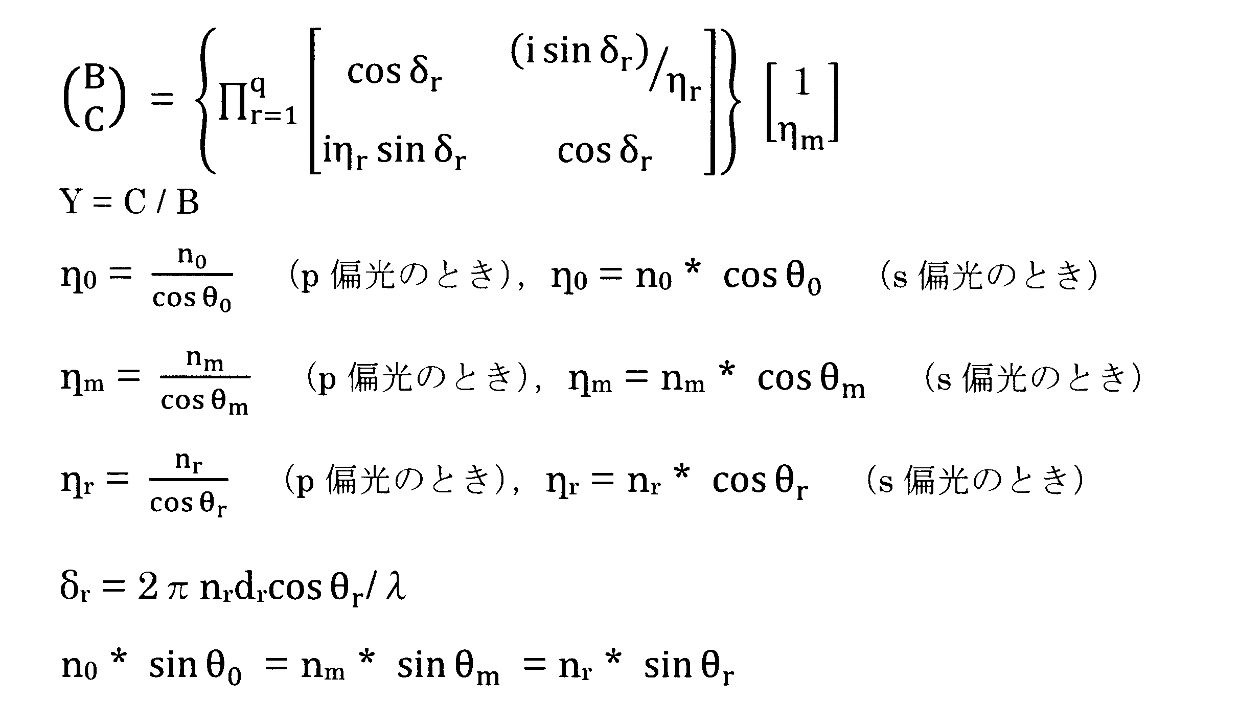
である。ここで、θ0は入射角、n0は入射媒質の屈折率、nrは多層膜の各層の屈折率、drは多層膜の各層の厚さ、nmは出射媒質の屈折率を表す。材料が吸収を持つような場合には、屈折率として、虚部として消衰係数を持つ複素屈折率を用いればよい。
実施形態2.
図5は、本発明の一態様による光学素子50の第2の実施形態を模式的に示す断面図である。図5に示すように、第2の実施形態では、光吸収層51および光吸収層52がフランジ部13の両面(表面側のフランジ面Aおよび裏面側のフランジ面B)に亘って成膜されている。そのような構成によって、光学素子10に入射した光が光学素子10から出射されるまでの経路において、光吸収層に入射する回数を増やすことができる。したがって、迷光の強度をより低減することができる。なお、図5には光学素子50の一断面が示されているが、平面図においては、フランジ部13の平坦部は環状であり、第1の曲面11の外周部から光学素子50の外径方向に向かって延在する。また、第1の実施形態と同様、使用波長帯において透明であれば、光学素子50の材質として、セラミックスやプラスチック、有機無機の混合材料などの材質を用いてもよい。
図5は、本発明の一態様による光学素子50の第2の実施形態を模式的に示す断面図である。図5に示すように、第2の実施形態では、光吸収層51および光吸収層52がフランジ部13の両面(表面側のフランジ面Aおよび裏面側のフランジ面B)に亘って成膜されている。そのような構成によって、光学素子10に入射した光が光学素子10から出射されるまでの経路において、光吸収層に入射する回数を増やすことができる。したがって、迷光の強度をより低減することができる。なお、図5には光学素子50の一断面が示されているが、平面図においては、フランジ部13の平坦部は環状であり、第1の曲面11の外周部から光学素子50の外径方向に向かって延在する。また、第1の実施形態と同様、使用波長帯において透明であれば、光学素子50の材質として、セラミックスやプラスチック、有機無機の混合材料などの材質を用いてもよい。
また、本実施形態でも、フランジ部13が粗面化されたり、粗面化されていないフランジ部13に対して墨が塗られるといったことはないので、フランジ面A,Bの精度を損なうことなく迷光を低減することが可能になる。
なお、本実施形態の光学素子50は、第1の実施形態の光学素子10と同様に成形可能である(図3および図4参照)。すなわち、例えば、真空蒸着、スパッタリング、CVD(Chemical Vapor Deposition)法を用いて成膜することができる。ただし、本実施形態では、真空蒸着またはスパッタリングを用いる場合、第1の実施形態と同様にして光吸収層51を成膜した後、蒸着源と第2の曲面12との間にマスク部材を設置して光吸収層52を成膜する。
本実施形態では、真空蒸着またはスパッタリングを用いる場合には第1の実施形態に対して成形のための工程が増えるが、光吸収層51と光吸収層52とを一括して成膜できる方法を用いてもよい。
実施形態3.
上記実施形態1、2では、フランジ部が粗面化されていない例を示した。フランジ部は粗面でない方が好ましいが、本発明の一態様はこれに限定されず、フランジ部が粗面化されたものを排除するものではない。フランジ部が粗面化される場合は、フランジ部の平坦度が損なわれないように粗面化されることが好ましい。フランジ部の平坦度が損なわれない粗面化とは、例えば以下のような粗面が好ましい。
粗面化されたフランジ部において、それぞれ100μm×100μmの隣り合う2つの領域を、第1の領域、第2の領域とする。第1の領域において、最も高い凸部を第1の凸部とする。第2の領域において、もっとも高い凸部を第2の凸部とする。第1の凸部と第2の凸部の高さの差が、5μm以内である。第1の凸部と第2の凸部の高さの差は、好ましくは3μm以内であり、より好ましくは2μm以内であり、さらに好ましくは1μm以内である。
フランジ部が粗面化される場合でも、粗面化されたフランジ部が上述の条件を満たすことで、フランジ面の精度が大きく損なわれることは防げる。また、粗面化されたフランジ部であっても上述の範囲を満たすことで、平坦な板をフランジ部に押し当てた場合に平坦な板の傾きを小さくすることができる。そのため、本発明の一態様の光学素子を用いて光学系を組み立てる際に、フランジ部を組み立ての基準として用いることができる。また、粗面化されたフランジ部であっても上述の範囲を満たすことで、平坦な板をフランジ部に押し当てた場合に変形やがたが生じてチルトが発生することを防止できる。
フランジ部が粗面化されている以外の構成は、実施形態1、2の構成に準じればよいため、詳細な説明は省略する。
上記実施形態1、2では、フランジ部が粗面化されていない例を示した。フランジ部は粗面でない方が好ましいが、本発明の一態様はこれに限定されず、フランジ部が粗面化されたものを排除するものではない。フランジ部が粗面化される場合は、フランジ部の平坦度が損なわれないように粗面化されることが好ましい。フランジ部の平坦度が損なわれない粗面化とは、例えば以下のような粗面が好ましい。
粗面化されたフランジ部において、それぞれ100μm×100μmの隣り合う2つの領域を、第1の領域、第2の領域とする。第1の領域において、最も高い凸部を第1の凸部とする。第2の領域において、もっとも高い凸部を第2の凸部とする。第1の凸部と第2の凸部の高さの差が、5μm以内である。第1の凸部と第2の凸部の高さの差は、好ましくは3μm以内であり、より好ましくは2μm以内であり、さらに好ましくは1μm以内である。
フランジ部が粗面化される場合でも、粗面化されたフランジ部が上述の条件を満たすことで、フランジ面の精度が大きく損なわれることは防げる。また、粗面化されたフランジ部であっても上述の範囲を満たすことで、平坦な板をフランジ部に押し当てた場合に平坦な板の傾きを小さくすることができる。そのため、本発明の一態様の光学素子を用いて光学系を組み立てる際に、フランジ部を組み立ての基準として用いることができる。また、粗面化されたフランジ部であっても上述の範囲を満たすことで、平坦な板をフランジ部に押し当てた場合に変形やがたが生じてチルトが発生することを防止できる。
フランジ部が粗面化されている以外の構成は、実施形態1、2の構成に準じればよいため、詳細な説明は省略する。
図6は、光学素子10を用いて組み立てられた光学系60を模式的に示す断面図である。図6に例示する光学系60では、鏡筒61の内部に、光学素子10、レンズ部材20およびスペーサ63が配置されている。図6には、第1の実施形態の光学素子10が例示されているが、第2の実施形態の光学素子50を用いてもよい。
上述したように、第1の実施形態では(第2の実施形態、第3の実施形態でも同様)、光学素子10におけるフランジ面A(または、フランジ面A,B)の精度が損なわれていないので、光学素子10と鏡筒61とのクリアランスを十分小さくすることができる。したがって、鏡筒61の開口の中心と光学素子10の軸を精度よく合わせることができる。また、光学素子10のフランジ面A(または、フランジ面A,B)は十分平坦であるため、フランジ部13を受ける鏡筒61の面とのチルトを発生させずに、光学素子10を鏡筒61に組みつけることができる。
本発明の一態様の光学素子(第1~第3の実施形態に示される光学素子)は、種々の光学系や光学装置に適用(例えば組み込み)可能である。すなわち、本発明の一態様は、本発明の一態様の光学素子を備えた光学系を提供できる。本発明の一態様の光学系は、光学素子に加えて、上記光学素子と共働するレンズ、反射防止フィルムやバンドパスフィルタなどの光学フィルタ、カバーガラス、絞り等を備えうる。ただし、これらは一例であって、本発明の一態様の光学素子の適用対象はこれら光学系に限られない。
また、本発明の一態様は、本発明の一態様の光学素子を備えた光学装置を提供できる。本発明の一態様の光学装置は、撮像素子を備えた撮像装置であってもよく、撮像素子を備えていない光学装置であってもよい。撮像装置としては、例えばカメラなどが挙げられる。
本発明の一態様の光学素子(第1~第3の実施形態に示される光学素子)は、種々の光学系や光学装置に適用(例えば組み込み)可能である。すなわち、本発明の一態様は、本発明の一態様の光学素子を備えた光学系を提供できる。本発明の一態様の光学系は、光学素子に加えて、上記光学素子と共働するレンズ、反射防止フィルムやバンドパスフィルタなどの光学フィルタ、カバーガラス、絞り等を備えうる。ただし、これらは一例であって、本発明の一態様の光学素子の適用対象はこれら光学系に限られない。
また、本発明の一態様は、本発明の一態様の光学素子を備えた光学装置を提供できる。本発明の一態様の光学装置は、撮像素子を備えた撮像装置であってもよく、撮像素子を備えていない光学装置であってもよい。撮像装置としては、例えばカメラなどが挙げられる。
次に、図1に示された第1の実施形態の光学素子10を用いた場合の実施例を説明する。屈折率1.52のガラスをガラスプリフォーム加工し、モールド成形によってレンズ形状(光吸収層14が成膜されていない状態の光学素子10)に成形する。光学素子10の端面はガラスの成形面となっている。フランジ部13の側面の粗さはRa0.1μm以下である。
このような光学素子10に対してマスク部材33を設置した状態で、スパッタリングによって、光吸収層14として酸化クロム(Cr2O3)、クロム(Cr)をそれぞれ60nm、10nm成膜する。したがって、このように成膜された光吸収層14の厚さは2μm以下になっている。
図7は、本実施例で用いた酸化クロムおよびクロムの屈折率と消衰係数とを示す説明図である。図7(a)に、酸化クロムの屈折率(Refractive Index)と消衰係数(Extinction coefficient)が示されている。図7(b)に、クロムの屈折率と消衰係数が示されている。図7において、n(破線)は屈折率を示し、k(実線)は消衰係数を示す。
図8は、本実施例の光吸収層14に対してガラス内で垂直に光が入射した場合の透過率(Transmittance)および反射率(Reflectance)の計算結果を示す説明図である。なお、透過率と反射率の値はp偏光とs偏光の平均値である。
図9(a)には、ガラス90内で光吸収層14に対して5°から85°までの範囲で光が入射した場合の反射率が示されている。なお、図9(b)には、透過率および反射率の計算の際に想定した構造であって、ガラス90に対して、酸化クロム(Cr2O3)が60nm成膜され、クロム(Cr)が10nm成膜された構造が例示されている。図9(a)に示すように、入射角度65°、すなわち光吸収層14の鉛直方向を基準とした65°の角度、においても400~700nmの波長帯域において反射率は30%以下になっている。また、入射角度65°において反射率の極小値が約560nmになっている。
図10は、酸化クロムとクロムとによる光吸収層14の膜厚が、図9(b)に示された光吸収層14に対して、70%(酸化クロム 42nm、クロム 7nm)、50%(酸化クロム 30nm、クロム 5nm)である場合の、入射角度65°の光の反射率が示されている。膜厚が薄くなることによって反射率の極小値が短波長側にシフトしているが、各厚さにおいて反射率は30%以下になっている。
以上のことから、本実施例の光学素子10では、全反射条件を満たす角度41°と最大入射角である90°との平均の入射角度65°において(ガラスの屈折率を1.52とする。)、反射率が十分小さくなっているといえる。すなわち、迷光が低減されることになる。
本発明を詳細にまた特定の実施態様を参照して説明したが、本発明の趣旨を逸脱することなく様々な変更や修正を加えることができることは当業者にとって明らかである。
本出願は、2018年7月26日出願の日本特許出願(特願2018-139972)に基づくものであり、その内容はここに参照として取り込まれる。
本発明によれば、フランジ面の精度を大きく損なうことなく迷光を低減できる。この効果を奏する本発明は、光学素子、光学系、および撮像光学装置に関して有用である。
10,50 光学素子
11 第1の曲面
12 第2の曲面
13 フランジ部
14,51,52 光吸収層
20 レンズ部材
30,31,32 蒸着材
33 マスク部材
60 光学系
61 鏡筒
63 スペーサ
11 第1の曲面
12 第2の曲面
13 フランジ部
14,51,52 光吸収層
20 レンズ部材
30,31,32 蒸着材
33 マスク部材
60 光学系
61 鏡筒
63 スペーサ
Claims (10)
- 曲面と、前記曲面から外径方向に延在する環状の平坦部を有するフランジ部とを含む光学素子であって、
前記フランジ部の少なくとも一部において、該光学素子の内部から光が入射したときの反射率を低減するための光吸収層を有し、
前記光吸収層の厚さが2μm以下である
ことを特徴とする光学素子。 - 前記光学素子は、ガラスで形成されている
請求項1に記載の光学素子。 - 前記フランジ部の最外面である側面に前記光吸収層を有する
請求項1または2に記載の光学素子。 - 該光学素子の内部から、前記光吸収層に、該光吸収層の鉛直方向を基準とした65°の角度で入射した光の、400nmから700nmの波長帯における反射率が50%以下である
請求項1~3のいずれか一項に記載の光学素子。 - 該光学素子の内部から、前記光吸収層に、該光吸収層の鉛直方向を基準とした65°の角度で入射した光の、400nmから700nmの波長帯における反射率が30%以下である
請求項4に記載の光学素子。 - 曲面と、前記曲面から外径方向に延在する環状で平坦部を有するフランジ部とを含む光学素子であって、
前記フランジ部の側面の算術平均粗さはRa0.1μm以下であり、
前記フランジ部の少なくとも一部において、金属、半導体または誘電体を含む光吸収層を有する
ことを特徴とする光学素子。 - 前記光学素子は、ガラスで形成されている
請求項6に記載の光学素子。 - 前記フランジ部の最外面である前記側面の算術平均粗さはRa0.01μm以下である
請求項6または7に記載の光学素子。 - 請求項1~8のいずれか一項に記載の光学素子を有する光学系。
- 請求項1~8のいずれか一項に記載の光学素子と撮像素子とを有する光学装置。
Priority Applications (2)
| Application Number | Priority Date | Filing Date | Title |
|---|---|---|---|
| JP2020532394A JPWO2020022295A1 (ja) | 2018-07-26 | 2019-07-22 | 光学素子、光学系、および光学装置 |
| CN201980049572.XA CN112470043A (zh) | 2018-07-26 | 2019-07-22 | 光学元件、光学系统、以及光学装置 |
Applications Claiming Priority (2)
| Application Number | Priority Date | Filing Date | Title |
|---|---|---|---|
| JP2018-139972 | 2018-07-26 | ||
| JP2018139972 | 2018-07-26 |
Publications (1)
| Publication Number | Publication Date |
|---|---|
| WO2020022295A1 true WO2020022295A1 (ja) | 2020-01-30 |
Family
ID=69182256
Family Applications (1)
| Application Number | Title | Priority Date | Filing Date |
|---|---|---|---|
| PCT/JP2019/028727 Ceased WO2020022295A1 (ja) | 2018-07-26 | 2019-07-22 | 光学素子、光学系、および光学装置 |
Country Status (3)
| Country | Link |
|---|---|
| JP (1) | JPWO2020022295A1 (ja) |
| CN (1) | CN112470043A (ja) |
| WO (1) | WO2020022295A1 (ja) |
Cited By (2)
| Publication number | Priority date | Publication date | Assignee | Title |
|---|---|---|---|---|
| WO2022045012A1 (ja) * | 2020-08-31 | 2022-03-03 | Agc株式会社 | 光学素子 |
| JP2022040845A (ja) * | 2020-08-31 | 2022-03-11 | Agc株式会社 | 光学素子 |
Citations (7)
| Publication number | Priority date | Publication date | Assignee | Title |
|---|---|---|---|---|
| JP2013095620A (ja) * | 2011-10-28 | 2013-05-20 | Olympus Corp | 光学素子、および光学素子の製造方法 |
| JP2013114235A (ja) * | 2011-12-01 | 2013-06-10 | Canon Inc | 光学素子、光学素子の製造方法、光学系および光学機器 |
| WO2014162846A1 (ja) * | 2013-04-04 | 2014-10-09 | コニカミノルタ株式会社 | レンズユニット及び撮像装置 |
| JP2015225102A (ja) * | 2014-05-26 | 2015-12-14 | コニカミノルタ株式会社 | 撮像レンズ、撮像装置及び携帯端末 |
| US9638832B1 (en) * | 2016-04-22 | 2017-05-02 | Genius Electronic Optical Co., Ltd. | Optical lens |
| JP2017173593A (ja) * | 2016-03-24 | 2017-09-28 | キヤノン株式会社 | 光学部材およびその製造方法 |
| JP2018146878A (ja) * | 2017-03-08 | 2018-09-20 | カンタツ株式会社 | レンズ素子および撮像レンズユニット |
Family Cites Families (11)
| Publication number | Priority date | Publication date | Assignee | Title |
|---|---|---|---|---|
| JP2008226390A (ja) * | 2007-03-15 | 2008-09-25 | Matsushita Electric Ind Co Ltd | 対物レンズ |
| JP4659848B2 (ja) * | 2008-03-06 | 2011-03-30 | オリンパスメディカルシステムズ株式会社 | 撮像モジュール |
| KR101791493B1 (ko) * | 2009-12-11 | 2017-10-30 | 후지필름 가부시키가이샤 | 흑색 경화성 조성물, 차광성 컬러필터, 차광막 및 그 제조 방법, 웨이퍼 레벨 렌즈, 및 고체 촬상 소자 |
| JP2012119046A (ja) * | 2010-12-03 | 2012-06-21 | Fujifilm Corp | レンズ及び光情報記録再生装置 |
| JP5662982B2 (ja) * | 2011-10-28 | 2015-02-04 | Hoya株式会社 | 反射防止膜および光学素子 |
| JP5849719B2 (ja) * | 2012-01-23 | 2016-02-03 | 旭硝子株式会社 | 光吸収体及びこれを用いた撮像装置 |
| JP6081753B2 (ja) * | 2012-09-14 | 2017-02-15 | 株式会社タムロン | 光学素子 |
| JP6080299B2 (ja) * | 2013-03-15 | 2017-02-15 | 富士フイルム株式会社 | 光学部材およびその製造方法 |
| CN104570168A (zh) * | 2013-10-16 | 2015-04-29 | 玉晶光电(厦门)有限公司 | 镜片、镜头及镜片的制造方法 |
| JP6742716B2 (ja) * | 2015-11-30 | 2020-08-19 | キヤノン株式会社 | 光学素子の製造方法、および光学機器の製造方法 |
| CN206115130U (zh) * | 2016-10-27 | 2017-04-19 | 四川长虹电器股份有限公司 | 一种dlp投影机的光学引擎系统 |
-
2019
- 2019-07-22 CN CN201980049572.XA patent/CN112470043A/zh active Pending
- 2019-07-22 JP JP2020532394A patent/JPWO2020022295A1/ja active Pending
- 2019-07-22 WO PCT/JP2019/028727 patent/WO2020022295A1/ja not_active Ceased
Patent Citations (7)
| Publication number | Priority date | Publication date | Assignee | Title |
|---|---|---|---|---|
| JP2013095620A (ja) * | 2011-10-28 | 2013-05-20 | Olympus Corp | 光学素子、および光学素子の製造方法 |
| JP2013114235A (ja) * | 2011-12-01 | 2013-06-10 | Canon Inc | 光学素子、光学素子の製造方法、光学系および光学機器 |
| WO2014162846A1 (ja) * | 2013-04-04 | 2014-10-09 | コニカミノルタ株式会社 | レンズユニット及び撮像装置 |
| JP2015225102A (ja) * | 2014-05-26 | 2015-12-14 | コニカミノルタ株式会社 | 撮像レンズ、撮像装置及び携帯端末 |
| JP2017173593A (ja) * | 2016-03-24 | 2017-09-28 | キヤノン株式会社 | 光学部材およびその製造方法 |
| US9638832B1 (en) * | 2016-04-22 | 2017-05-02 | Genius Electronic Optical Co., Ltd. | Optical lens |
| JP2018146878A (ja) * | 2017-03-08 | 2018-09-20 | カンタツ株式会社 | レンズ素子および撮像レンズユニット |
Cited By (5)
| Publication number | Priority date | Publication date | Assignee | Title |
|---|---|---|---|---|
| WO2022045012A1 (ja) * | 2020-08-31 | 2022-03-03 | Agc株式会社 | 光学素子 |
| JPWO2022045012A1 (ja) * | 2020-08-31 | 2022-03-03 | ||
| JP2022040845A (ja) * | 2020-08-31 | 2022-03-11 | Agc株式会社 | 光学素子 |
| JP7577946B2 (ja) | 2020-08-31 | 2024-11-06 | Agc株式会社 | 光学素子 |
| JP7647759B2 (ja) | 2020-08-31 | 2025-03-18 | Agc株式会社 | 光学素子 |
Also Published As
| Publication number | Publication date |
|---|---|
| CN112470043A (zh) | 2021-03-09 |
| JPWO2020022295A1 (ja) | 2021-08-02 |
Similar Documents
| Publication | Publication Date | Title |
|---|---|---|
| US9158039B2 (en) | Optical element, and optical system and optical apparatus using same | |
| TWI676852B (zh) | 遮光片 | |
| JP6006718B2 (ja) | 光学フィルタ、光学機器、電子機器及び反射防止複合体 | |
| US7839582B2 (en) | Optical element | |
| US7626772B2 (en) | Optical system and optical apparatus having the same | |
| CN112882137A (zh) | 成像镜头、相机模块及电子装置 | |
| WO2012157719A1 (ja) | 光学フィルタ及び光学装置 | |
| US20090316262A1 (en) | Transmission type polarizing element, and composite polarizing plate using the element | |
| JP6923998B2 (ja) | 光学部材およびその製造方法 | |
| KR20210035516A (ko) | 폴디드 카메라 모듈 및 그것을 갖는 모바일 장치 | |
| US8559112B2 (en) | Optical element | |
| US7787184B2 (en) | Member having antireflection structure | |
| JP4568810B1 (ja) | 薄膜型光吸収膜 | |
| JPWO2020022295A1 (ja) | 光学素子、光学系、および光学装置 | |
| US10996376B2 (en) | Optical element and optical system including the same | |
| US9594192B2 (en) | Optical element, optical system, and method of manufacturing optical element | |
| TWI750707B (zh) | 墊圈 | |
| JP4598379B2 (ja) | 絞り構造体およびこれを備えた複合レンズ装置 | |
| JP6053352B2 (ja) | 光学フィルタ、光学装置及び光学フィルタの製造方法。 | |
| JP2010175941A (ja) | 光学フィルタ及び光学フィルタの製造方法、並びにこれらの光学フィルタを有する撮像装置 | |
| JP2004258494A (ja) | Ndフィルタ | |
| US11513440B2 (en) | Optical element, optical system, and optical apparatus | |
| JP7475129B2 (ja) | 遮光部材、遮光部材を用いた撮像装置 | |
| JP4963027B2 (ja) | Ndフィルタおよびその製造方法、それらを用いた光量絞り装置 | |
| US20180024275A1 (en) | Optical member and method for manufacturing the same |
Legal Events
| Date | Code | Title | Description |
|---|---|---|---|
| 121 | Ep: the epo has been informed by wipo that ep was designated in this application |
Ref document number: 19842320 Country of ref document: EP Kind code of ref document: A1 |
|
| ENP | Entry into the national phase |
Ref document number: 2020532394 Country of ref document: JP Kind code of ref document: A |
|
| NENP | Non-entry into the national phase |
Ref country code: DE |
|
| 122 | Ep: pct application non-entry in european phase |
Ref document number: 19842320 Country of ref document: EP Kind code of ref document: A1 |