WO2020021642A1 - 回路パッケージの製造方法及び回路パッケージ - Google Patents
回路パッケージの製造方法及び回路パッケージ Download PDFInfo
- Publication number
- WO2020021642A1 WO2020021642A1 PCT/JP2018/027759 JP2018027759W WO2020021642A1 WO 2020021642 A1 WO2020021642 A1 WO 2020021642A1 JP 2018027759 W JP2018027759 W JP 2018027759W WO 2020021642 A1 WO2020021642 A1 WO 2020021642A1
- Authority
- WO
- WIPO (PCT)
- Prior art keywords
- circuit
- circuits
- sealing
- insulating material
- circuit package
- Prior art date
- Legal status (The legal status is an assumption and is not a legal conclusion. Google has not performed a legal analysis and makes no representation as to the accuracy of the status listed.)
- Ceased
Links
Images

Classifications
-
- H—ELECTRICITY
- H05—ELECTRIC TECHNIQUES NOT OTHERWISE PROVIDED FOR
- H05K—PRINTED CIRCUITS; CASINGS OR CONSTRUCTIONAL DETAILS OF ELECTRIC APPARATUS; MANUFACTURE OF ASSEMBLAGES OF ELECTRICAL COMPONENTS
- H05K3/00—Apparatus or processes for manufacturing printed circuits
- H05K3/22—Secondary treatment of printed circuits
- H05K3/28—Applying non-metallic protective coatings
-
- H—ELECTRICITY
- H10—SEMICONDUCTOR DEVICES; ELECTRIC SOLID-STATE DEVICES NOT OTHERWISE PROVIDED FOR
- H10W—GENERIC PACKAGES, INTERCONNECTIONS, CONNECTORS OR OTHER CONSTRUCTIONAL DETAILS OF DEVICES COVERED BY CLASS H10
- H10W74/00—Encapsulations, e.g. protective coatings
-
- H—ELECTRICITY
- H10—SEMICONDUCTOR DEVICES; ELECTRIC SOLID-STATE DEVICES NOT OTHERWISE PROVIDED FOR
- H10W—GENERIC PACKAGES, INTERCONNECTIONS, CONNECTORS OR OTHER CONSTRUCTIONAL DETAILS OF DEVICES COVERED BY CLASS H10
- H10W90/00—Package configurations
-
- H—ELECTRICITY
- H10—SEMICONDUCTOR DEVICES; ELECTRIC SOLID-STATE DEVICES NOT OTHERWISE PROVIDED FOR
- H10W—GENERIC PACKAGES, INTERCONNECTIONS, CONNECTORS OR OTHER CONSTRUCTIONAL DETAILS OF DEVICES COVERED BY CLASS H10
- H10W72/00—Interconnections or connectors in packages
- H10W72/851—Dispositions of multiple connectors or interconnections
- H10W72/874—On different surfaces
- H10W72/884—Die-attach connectors and bond wires
-
- H—ELECTRICITY
- H10—SEMICONDUCTOR DEVICES; ELECTRIC SOLID-STATE DEVICES NOT OTHERWISE PROVIDED FOR
- H10W—GENERIC PACKAGES, INTERCONNECTIONS, CONNECTORS OR OTHER CONSTRUCTIONAL DETAILS OF DEVICES COVERED BY CLASS H10
- H10W90/00—Package configurations
- H10W90/701—Package configurations characterised by the relative positions of pads or connectors relative to package parts
- H10W90/751—Package configurations characterised by the relative positions of pads or connectors relative to package parts of bond wires
- H10W90/753—Package configurations characterised by the relative positions of pads or connectors relative to package parts of bond wires between laterally-adjacent chips
Definitions
- the present disclosure relates to a method for manufacturing a circuit package and a circuit package.
- a printed board is generally manufactured by attaching a metal foil to a board, etching the metal foil, and processing it into a desired circuit shape.
- the current capacity of the circuit board can be increased by increasing the cross-sectional area of the circuit (ie, increasing the thickness of the circuit).
- circuit sheet in which a circuit is insulated after a metal plate is processed into a circuit (circuit sheet) is first prepared, and the circuit sheet is placed on a substrate.
- a process for forming a circuit sheet is required, and there is a problem in terms of production efficiency as compared with the conventional method.
- insulation between circuits and sealing around the circuits are performed in different processes, respectively, so that an insulating portion between circuits and sealing around the circuits are sealed. There is an interface between the parts, and there is room for improvement from the viewpoint of insulation reliability.
- circuit package manufacturing method capable of efficiently manufacturing a circuit package having a large current capacity and excellent insulation reliability.
- Another object of the present disclosure is to provide a circuit package having a large current capacity and excellent insulation reliability.
- ⁇ 1> A method for manufacturing a circuit package, comprising: a step of arranging circuits on a base material; and a step of performing sealing between the circuits and sealing around the circuits using the same insulating material in this order. .
- ⁇ 2> The method for manufacturing a circuit package according to ⁇ 1>, wherein the thickness of the circuit is 350 ⁇ m or more.
- ⁇ 3> The method for producing a circuit package according to ⁇ 1> or ⁇ 2>, wherein the insulating material has an elastic modulus at 25 ° C. of 5 GPa to 25 GPa.
- ⁇ 4> Sealing between the circuits and sealing around the circuits are performed by a method including a step of supplying the insulating material to the inside of the mold in which the circuits are arranged without applying pressure.
- ⁇ 5> The sealing according to ⁇ 4>, wherein the sealing between the circuits and the sealing around the circuits include a step of reducing the pressure inside the mold after supplying the insulating material into the mold.
- a circuit package comprising: a circuit; and a sealing portion disposed between and around the circuit and formed around the same insulating material.
- ⁇ 7> The circuit package according to ⁇ 6>, wherein the thickness of the circuit is 350 ⁇ m or more.
- a method of manufacturing a circuit package that can efficiently manufacture a circuit package having a large current capacity and excellent insulation reliability is provided.
- a circuit package having a large current capacity and excellent insulation reliability is provided.
- FIG. 4 is a diagram schematically illustrating steps of a method of manufacturing a circuit package according to the present disclosure. It is a figure showing roughly the process of the manufacturing method of the conventional circuit package.
- the present invention is not limited to the following embodiments.
- the components including the element steps and the like
- the term "step” includes, in addition to a step independent of other steps, even if the purpose of the step is achieved even if it cannot be clearly distinguished from the other steps, the step is also included.
- the numerical ranges indicated by using “to” include the numerical values described before and after “to” as the minimum value and the maximum value, respectively.
- each component may include a plurality of corresponding substances.
- the content or content of each component is, unless otherwise specified, the total content or content of the plurality of substances present in the composition. Means quantity.
- the term "layer” includes, when observing a region where the layer exists, in addition to a case where the layer is formed over the entire region and a case where the layer is formed only on a part of the region. included.
- laminate refers to stacking layers, where two or more layers may be joined, or two or more layers may be removable.
- ⁇ Circuit package manufacturing method> In the method of manufacturing a circuit package according to the present disclosure, a step of arranging a circuit on a base material (a circuit arranging step), and sealing between the circuits and sealing around the circuit are performed using the same insulating material. And a process (sealing process) in this order.
- a circuit package having a large current capacity can be efficiently manufactured. More specifically, an uninsulated circuit is placed on a substrate instead of a circuit sheet in which the circuit is insulated, and then the sealing between the circuits and the sealing around the circuit are the same. The number of steps is reduced by using an insulating material. Furthermore, in the circuit package manufactured by the above method, the interface between the different materials is not formed in the sealing portion as compared with the case where the sealing between the circuits and the sealing around the circuit are performed with different materials, so that the insulation reliability is improved. Better.
- the step of performing sealing between circuits and sealing around the circuits using the same insulating material is preferably performed collectively. More specifically, the time from the start to the end of the step of sealing between circuits and the time from the start to the end of the step of sealing the periphery of the circuit completely or partially match. preferable.
- between circuits means a portion of a space separating conductors constituting the circuit, and “around the circuit” corresponds to a top surface and a side surface (outer peripheral portion of the circuit) of the circuit. Means part.
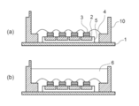
- FIG. 1 is a diagram schematically illustrating steps of a method of manufacturing a circuit package according to the present disclosure
- FIG. 2 is a diagram schematically illustrating steps of a method of manufacturing a conventional circuit package.
- the circuit 2 is arranged on the base material 1, the element 3 is mounted on the circuit 2, and the wires 3 are connected between the elements 3 (a).
- the circuit 2 has not yet been isolated at this stage.
- the method of arranging the circuit 2 on the substrate 1 is not particularly limited. From the viewpoint of suppressing the displacement of the circuit 2, the surface opposite to the transfer sheet of the circuit 2 is placed on the substrate 1 in a state where the transfer sheet is disposed on the surface of the circuit 2 opposite to the side in contact with the substrate 1. A method of arranging and removing the transfer sheet is preferable.
- a frame 10 is provided to supply and seal an insulating material between and around the circuits 2.
- the insulating material 6 is supplied into the frame 10, and the space between the circuits 2 and the space around the circuit 2 are filled with the insulating material 6, and the insulating material 6 is cured if necessary. (B).
- a temporary package may be used as the substrate 1, and the circuit 2 from which the temporary substrate has been removed after sealing may be arranged on another substrate to produce a circuit package. Further, it may be used as a part of a circuit package (for example, an insulating layer) without removing the base material 1.
- the circuit 2 is arranged on the base material 1, the element 3 is mounted on the circuit 2, and the wires 3 are connected between the elements 3 (a).
- the space between the circuits 2 is filled with a resin 5 for insulation.
- a frame 10 is arranged to seal the periphery of the circuit 2.
- a circuit sheet (circuit sheet) filled with resin 5 between circuits 2 is used. Illustration of the circuit sheet manufacturing process is omitted.
- a resin sheet a step of preparing a circuit disposed on a temporary fixing material such as a mold, a step of filling a resin between the circuits, and a step of filling a resin between the circuits, Removing the temporary fixing material from the circuit.
- a temporary substrate is used as the substrate 1, and after sealing, the circuit from which the temporary substrate has been removed is placed on a substrate to produce a circuit package. Is also good. Further, it may be used as a part of a circuit package (for example, an insulating layer) without removing the base material 1.
- the space between the circuits 2 and the periphery thereof are collectively sealed with the insulating material 6. There is no need to prepare a circuit sheet filled with the resin 5.
- the space between the circuits 2 and the periphery thereof are collectively sealed with the insulating material 6, the space between the resin 5 filling the space between the circuits 2 and the insulating material 6 as in the conventional method shown in FIG. No interface is formed.
- the type of circuit used in the above method is not particularly limited.
- Examples of the material of the circuit include copper, silver, chromium copper, tungsten copper, nickel, nickel-plated copper, aluminum, and aluminum whose surface is modified with alumite. It is preferable to contain copper from the viewpoint of conductivity.
- the thickness of the circuit is not particularly limited, and can be selected according to the use of the circuit package. From the viewpoint of increasing the current of the circuit package, the thickness of the circuit is preferably 350 ⁇ m or more, more preferably 400 ⁇ m or more, further preferably 500 ⁇ m or more, and particularly preferably 1000 ⁇ m or more. . From the viewpoint of the volume of the circuit package itself, the thickness of the circuit may be 5000 ⁇ m or less. If the thickness differs depending on the location of the circuit, the above-mentioned value may be the arithmetic average value of the measured values obtained at arbitrarily selected five locations.
- the thickness of the circuit means the thickness of the circuit itself, and when a part of the circuit is embedded in an adjacent member, the thickness of the embedded part is also included in the thickness of the circuit.
- the width and length of the circuit in the circuit package are not particularly limited, and may be selected according to the use of the circuit package.
- the width and length of the circuit may each be between 350 ⁇ m and 70000 ⁇ m.
- the arithmetic average of the measured values obtained at five arbitrarily selected locations may be used as the above value.
- the circuit is obtained, for example, by processing a metal plate into a circuit having a desired shape.
- the processing method is not particularly limited, and can be performed by a known method such as punching and cutting.
- the substrate used in the above method is not particularly limited as long as it can seal between the circuits and around the circuit in a state where the circuits are arranged on the substrate.
- the thickness of the substrate is not particularly limited, and can be selected according to the shape and thickness of the circuit. For example, it may be in the range of 1 ⁇ m to 150 ⁇ m.
- the base material is a part of the circuit package that is not removed in the circuit package manufacturing process, even if it is removed after sealing between the circuits and around the circuit (temporary base material). It may be.
- the base material is a temporary base material
- the arithmetic mean surface roughness (Rz) of the surface of the temporary base material in contact with the circuit is 0.01 ⁇ m to 30 ⁇ m from the viewpoint of easy removal from the circuit. , More preferably 0.05 ⁇ m to 25 ⁇ m, even more preferably 0.1 ⁇ m to 20 ⁇ m.
- the arithmetic average surface roughness of the temporary base material can be measured by a surface roughness measuring device (for example, a shape analysis laser microscope @ VK-X1000 (Keyence Corporation)).
- a surface roughness measuring device for example, a shape analysis laser microscope @ VK-X1000 (Keyence Corporation)
- the base material is a temporary base material
- the difference between the linear expansion coefficient of the temporary base material and the linear expansion coefficient of the circuit is reduced from the viewpoint of suppressing separation from the circuit in the step of sealing between and around the circuit. Is preferably small.
- the linear expansion coefficient of the temporary base material is, for example, preferably 0.1 ppm / K to 1000 ppm / K, more preferably 5 ppm / K to 500 ppm / K, and more preferably 10 ppm / K to 200 ppm / K. Is more preferred.
- the coefficient of linear expansion of a substrate or a circuit is measured when the temperature is increased at a constant rate using a thermomechanical analyzer (eg, a thermomechanical analyzer TMA / SS-6000 (Hitachi High-Tech Science Co., Ltd.)). It can be obtained by measuring the amount of thermal expansion of the measurement sample from the difference in the amount of thermal expansion between the sample and the standard sample.
- the measurement conditions can be set, for example, as follows. Load: 20g Measurement temperature: 30 ° C to 280 ° C Heating temperature: 5 ° C / min
- the base material contains a resin from the viewpoint of easy removal from the circuit.
- the temporary base material containing a resin include a resin sheet having a support film and an adhesive layer disposed on a side of the support film that contacts a circuit. Such arrangement of the circuit on the resin sheet can be performed by bringing the circuit into contact with the adhesive layer of the resin sheet and applying pressure and temperature as needed.
- the resin sheet may have an adhesive layer on at least one surface, that is, the surface that comes into contact with the circuit. From the viewpoint of easy removal from the circuit, the resin sheet preferably has flexibility.
- the material of the support film of the resin sheet is not particularly limited, and aromatic polyimide, aromatic polyamide, aromatic polysulfone, aromatic polyether sulfone, polyphenylene sulfide, aromatic polyether ketone, polyarylate, aromatic polyether ether ketone and It is preferably selected from the group consisting of polyethylene terephthalate.
- a layer containing a thermoplastic resin can be mentioned.
- a layer containing a thermoplastic resin having at least one selected from the group consisting of an amide group, an ester group, an imide group, an ether group, and a sulfone group may be mentioned.
- An adhesive may be further applied to the adhesive layer.
- the adhesive include an acrylic adhesive, a urethane adhesive, and a silicone adhesive.
- an adhesive refers to a substance capable of bonding an object by interposing between the objects.
- the glass transition temperature of the adhesive layer of the resin sheet is not particularly limited, and is preferably from 100 ° C. to 300 ° C.
- the glass transition temperature can be measured by dynamic viscoelasticity measurement.
- the temperature at which the mass of the adhesive layer decreases by 5% by mass when heated from normal temperature (25 ° C.) is preferably 300 ° C. or higher.
- the substrate used in the above method may be prepared or a commercially available substrate may be used.
- the resin sheet having the support film and the adhesive layer include a fixing tape for a lead frame (trade name: R-970, Tomagawa Paper Co., Ltd.) and a tape for encapsulation molding (trade name: RT-321, Hitachi Chemical Co., Ltd.) Etc. are commercially available.
- the insulating material used for sealing between and around the circuits is not particularly limited.
- it may include a resin.
- the resin include resins such as an epoxy resin, a phenol resin, a urea resin, a melamine resin, a urethane resin, a silicone resin, an unsaturated polyester resin, and an acrylic resin, and a curable resin is preferable.
- the resin contained in the insulating material may be one kind or two or more kinds.
- the insulating material preferably contains at least one selected from the group consisting of an epoxy resin, a silicone resin, and a urethane resin, and more preferably contains an epoxy resin.
- the state of the insulating material when it is supplied between the circuits and around the circuits may be liquid or solid.
- the term “liquid” means that the viscosity measured at 25 ° C. by using an E-type viscometer (for example, TV-33 (Toki Sangyo Co., Ltd.)) at 5 revolutions / minute (rpm). It means 1000 Pa ⁇ s or less.
- the insulating material may include components other than the resin, such as a filler, if necessary.
- the filler may be powdery or fibrous.
- the insulating material (the cured product of the insulating material when containing a curable resin) preferably has an elastic modulus (storage elastic modulus) at 25 ° C. of 5 GPa to 25 GPa, and more preferably 10 GPa to 20 GPa. More preferred.
- the elastic modulus at 25 ° C. is 5 GPa or more
- the circuit shape after the removal of the temporary base material is easily maintained, and the workability tends to be excellent.
- the elastic modulus at 25 ° C. is 25 GPa or less, stress generated due to a difference in thermal expansion coefficient between a sealing portion formed using an insulating material and another member tends to be reduced. .
- the elastic modulus at 25 ° C. of the insulating material can be measured by the following method.
- a cured product having a size of 10 mm ⁇ 50 mm ⁇ 3 mm was prepared, and the temperature was raised from 25 ° C. to 300 ° C. at a rate of 10 ° C./min using a thermomechanical analyzer (eg, “RSAIII” manufactured by TA Instruments).
- a thermomechanical analyzer eg, “RSAIII” manufactured by TA Instruments.
- GPa thermomechanical analyzer
- the method for sealing between circuits and the periphery of the circuits is not particularly limited.
- a method using a solid insulating material such as a powder include a casting method, an extrusion molding method, a compression molding method, a transfer molding method, and an insert molding method.
- a method using a liquid resin material include a casting method, a coating method, a printing method, and an embedding method.
- the sealing between and around the circuits is performed by a method that includes supplying the non-pressurized insulating material into the mold in which the circuits are located.
- a method that includes supplying the non-pressurized insulating material into the mold in which the circuits are located.
- non-pressure molding method such a method is also referred to as a “non-pressure molding method”.
- the sealing step can be generally performed with simple equipment as compared with a method such as a transfer molding method in which an insulating material is supplied into a mold while being pressed.
- generation of voids in the sealing portion can be suppressed more effectively, which is excellent in reliability.
- the non-press forming method is also applied to the case where the pressure is applied after supplying the insulating material to the inside of the mold. Shall be included.
- the method of supplying the insulating material to the inside of the mold without applying pressure is not particularly limited. For example, it may be performed by supplying an insulating material into an unsealed mold.
- the insulating material supplied inside the mold may be solid or liquid.
- the pressure inside the mold after supplying the insulating material to the inside of the mold for example, when the insulating material supplied to the inside of the mold is in the form of particles, the air existing between the particles is melted The formation of air bubbles remaining inside the insulating material can be suppressed.
- the method for performing the pressure increasing step is not particularly limited.
- a method may be used in which an opening of a mold whose inside is decompressed is opened to make it atmospheric pressure.
- the pressure reducing step is preferably performed before the step of melting the insulating material supplied into the mold (melting step).
- the pressure increasing step is performed after the melting step.
- a circuit package manufactured by the method of manufacturing a circuit package according to the present disclosure may include a circuit, a sealing unit disposed between and around the circuit, and a substrate.
- the type of the substrate is not particularly limited. For example, those generally used for the purpose of supporting a circuit, dissipating heat generated from elements mounted on the circuit, and the like may be used.
- the substrate may be a combination of a plurality of members (for example, a combination of a metal plate and an insulating layer for insulating the metal plate and a circuit).
- the substrate includes a metal plate
- its type is not particularly limited.
- copper, copper alloys such as aluminum tungsten copper and molybdenum copper, nickel-plated copper, and the like can be given.
- the shape, thickness, and the like of the metal plate are not particularly limited, and can be selected according to the use of the circuit package.
- the type of the insulating layer is not particularly limited.
- the insulating layer may include a resin.
- the resin contained in the insulating layer is not particularly limited, and includes curable resins such as epoxy resin, phenol resin, urea resin, melamine resin, urethane resin, silicone resin, unsaturated polyester resin, and acrylic resin.
- the resin contained in the insulating layer may be one type or two or more types.
- the insulating layer may include components other than resin, such as a filler, if necessary.
- the filler may be powdery or fibrous.
- the thickness of the insulating layer is not particularly limited, and may be selected according to the use of the circuit package. From the viewpoint of securing sufficient insulation, the thickness of the insulating layer is preferably as large as possible. For example, the thickness of the insulating layer is preferably at least 60 ⁇ m, more preferably at least 90 ⁇ m, even more preferably at least 120 ⁇ m.
- the thickness of the insulating layer is preferably 230 ⁇ m or less, more preferably 210 ⁇ m or less, and still more preferably 190 ⁇ m or less.
- a circuit package according to an embodiment of the present disclosure includes a circuit, and a sealing unit that is disposed between and around the circuit and that is integrally formed of the same insulating material.
- a sealing portion for sealing between circuits and a sealing portion for sealing the periphery of the circuit are collectively formed from the same insulating material. For this reason, when a sealing portion that seals between circuits and a sealing portion that seals the periphery of the circuit are formed in different processes, such as a circuit package manufactured using a conventional circuit sheet. In comparison, connection reliability is excellent.
- whether or not the sealing portions disposed between and around the circuit are formed of the same insulating material corresponds to, for example, between the circuits of the sealing portion.
- the determination can be made based on whether or not the types and proportions of the components included in the portion and the portion corresponding to the periphery of the circuit are the same.
- whether or not the sealing portion disposed between the circuits and around the circuit is formed collectively is, for example, a portion corresponding to between the circuits of the sealing portion
- the determination can be made based on whether or not an interface is formed between a portion corresponding to the periphery of the circuit.
- the circuit package of the present disclosure can be manufactured by, for example, the above-described circuit package manufacturing method.
- the details and preferred aspects of the circuit package and its members described in the above-described method of manufacturing the circuit package can be applied to the circuit package of the present disclosure.
Landscapes
- Engineering & Computer Science (AREA)
- Manufacturing & Machinery (AREA)
- Microelectronics & Electronic Packaging (AREA)
- Encapsulation Of And Coatings For Semiconductor Or Solid State Devices (AREA)
- Structures Or Materials For Encapsulating Or Coating Semiconductor Devices Or Solid State Devices (AREA)
Abstract
基材上に回路を配置する工程と、前記回路の間の封止と前記回路の周囲の封止を同じ絶縁性材料を用いて行う工程と、をこの順に備える回路パッケージの製造方法。
Description
本開示は、回路パッケージの製造方法及び回路パッケージに関する。
電子機器の小型化及び高機能化の進展に伴い、電子部品を基板上に高密度実装することが可能な回路基板としてプリント基板が広く用いられている。プリント基板は一般に、基板に金属箔を貼り付け、これをエッチングして所望の回路形状に加工することで製造されている。
一方、電子機器の使用環境の多様化に伴い、回路基板の電流容量の増大(大電流化)が求められている。回路基板の電流容量は、回路の断面積を大きくする(すなわち、回路の厚みを厚くする)することで増大させることができる。
大電流化に対応した回路基板を製造する方法として、金属板の打ち抜き加工等により形成した回路を用いる方法が提案されている(例えば、特許文献1参照)。
特許文献1に記載の方法では、金属板を回路に加工した後に回路間を絶縁した状態のもの(回路シート)をまず作製し、これを基板上に配置し、回路の周囲を絶縁性材料を用いて封止して回路パッケージを製造する。このため、回路シートを形成するための工程が必要となり、従来の方法に比べると生産効率の面で課題がある。
また、特許文献1に記載の方法で製造された回路パッケージは、回路の間の絶縁と回路の周囲の封止をそれぞれ異なる工程で行うため、回路の間の絶縁部と回路の周囲の封止部の間に界面が生じ、絶縁信頼性の観点から改善の余地がある。
また、特許文献1に記載の方法で製造された回路パッケージは、回路の間の絶縁と回路の周囲の封止をそれぞれ異なる工程で行うため、回路の間の絶縁部と回路の周囲の封止部の間に界面が生じ、絶縁信頼性の観点から改善の余地がある。
上記事情に鑑み、本開示の一態様は、電流容量が大きく、絶縁信頼性に優れる回路パッケージを効率よく製造できる回路パッケージの製造方法を提供することを課題とする。本開示の別の一態様は、電流容量が大きく、絶縁信頼性に優れる回路パッケージを提供することを課題とする。
上記課題を提供するための具体的な手段には、以下の実施態様が含まれる。
<1>基材上に回路を配置する工程と、前記回路の間の封止と前記回路の周囲の封止を同じ絶縁性材料を用いて行う工程と、をこの順に備える回路パッケージの製造方法。
<2>前記回路の厚さは350μm以上である、<1>に記載の回路パッケージの製造方法。
<3>前記絶縁性材料の25℃での弾性率が5GPa~25GPaである、<1>又は<2>に記載の回路パッケージの製造方法。
<4>前記回路の間の封止と前記回路の周囲の封止は、前記回路を配置した型の内部に前記絶縁性材料を非加圧で供給する工程を含む方法によって行う、<1>~<3>のいずれか1項に記載の回路パッケージの製造方法。
<5>前記回路の間の封止と前記回路の周囲の封止は、前記絶縁性材料を型の内部に供給した後、前記型の内部を減圧する工程を含む、<4>に記載の回路パッケージの製造方法。
<6>回路と、前記回路の間及び前記回路の周囲に配置され、同じ絶縁性材料から一括して形成された封止部と、を備える回路パッケージ。
<7>前記回路の厚さは350μm以上である、<6>に記載の回路パッケージ。
<8>前記絶縁性材料の25℃での弾性率が5GPa~25GPaである、<6>又は<7>に記載の回路パッケージ。
<1>基材上に回路を配置する工程と、前記回路の間の封止と前記回路の周囲の封止を同じ絶縁性材料を用いて行う工程と、をこの順に備える回路パッケージの製造方法。
<2>前記回路の厚さは350μm以上である、<1>に記載の回路パッケージの製造方法。
<3>前記絶縁性材料の25℃での弾性率が5GPa~25GPaである、<1>又は<2>に記載の回路パッケージの製造方法。
<4>前記回路の間の封止と前記回路の周囲の封止は、前記回路を配置した型の内部に前記絶縁性材料を非加圧で供給する工程を含む方法によって行う、<1>~<3>のいずれか1項に記載の回路パッケージの製造方法。
<5>前記回路の間の封止と前記回路の周囲の封止は、前記絶縁性材料を型の内部に供給した後、前記型の内部を減圧する工程を含む、<4>に記載の回路パッケージの製造方法。
<6>回路と、前記回路の間及び前記回路の周囲に配置され、同じ絶縁性材料から一括して形成された封止部と、を備える回路パッケージ。
<7>前記回路の厚さは350μm以上である、<6>に記載の回路パッケージ。
<8>前記絶縁性材料の25℃での弾性率が5GPa~25GPaである、<6>又は<7>に記載の回路パッケージ。
本開示の一態様によれば、電流容量が大きく、絶縁信頼性に優れる回路パッケージを効率よく製造できる回路パッケージの製造方法が提供される。本開示の別の一態様によれば、電流容量が大きく、絶縁信頼性に優れる回路パッケージが提供される。
以下、本発明を実施するための形態について詳細に説明する。但し、本発明は以下の実施形態に限定されるものではない。
以下の実施形態において、その構成要素(要素ステップ等も含む)は、特に明示した場合を除き、必須ではない。数値及びその範囲についても同様であり、本発明を制限するものではない。
本開示において「工程」との語には、他の工程から独立した工程に加え、他の工程と明確に区別できない場合であってもその工程の目的が達成されれば、当該工程も含まれる。
本開示において「~」を用いて示された数値範囲には、「~」の前後に記載される数値がそれぞれ最小値及び最大値として含まれる。
本開示中に段階的に記載されている数値範囲において、一つの数値範囲で記載された上限値又は下限値は、他の段階的な記載の数値範囲の上限値又は下限値に置き換えてもよい。また、本開示中に記載されている数値範囲において、その数値範囲の上限値又は下限値は、実施例に示されている値に置き換えてもよい。
本開示において各成分は該当する物質を複数種含んでいてもよい。組成物中に各成分に該当する物質が複数種存在する場合、各成分の含有率又は含有量は、特に断らない限り、組成物中に存在する当該複数種の物質の合計の含有率又は含有量を意味する。
本開示において「層」との語には、当該層が存在する領域を観察したときに、当該領域の全体に形成されている場合に加え、当該領域の一部にのみ形成されている場合も含まれる。
本開示において「積層」との語は、層を積み重ねることを示し、二以上の層が結合されていてもよく、二以上の層が着脱可能であってもよい。
本開示において実施形態を図面を参照して説明する場合、当該実施形態の構成は図面に示された構成に限定されない。また、各図における部材の大きさは概念的なものであり、部材間の大きさの相対的な関係はこれに限定されない。
以下の実施形態において、その構成要素(要素ステップ等も含む)は、特に明示した場合を除き、必須ではない。数値及びその範囲についても同様であり、本発明を制限するものではない。
本開示において「工程」との語には、他の工程から独立した工程に加え、他の工程と明確に区別できない場合であってもその工程の目的が達成されれば、当該工程も含まれる。
本開示において「~」を用いて示された数値範囲には、「~」の前後に記載される数値がそれぞれ最小値及び最大値として含まれる。
本開示中に段階的に記載されている数値範囲において、一つの数値範囲で記載された上限値又は下限値は、他の段階的な記載の数値範囲の上限値又は下限値に置き換えてもよい。また、本開示中に記載されている数値範囲において、その数値範囲の上限値又は下限値は、実施例に示されている値に置き換えてもよい。
本開示において各成分は該当する物質を複数種含んでいてもよい。組成物中に各成分に該当する物質が複数種存在する場合、各成分の含有率又は含有量は、特に断らない限り、組成物中に存在する当該複数種の物質の合計の含有率又は含有量を意味する。
本開示において「層」との語には、当該層が存在する領域を観察したときに、当該領域の全体に形成されている場合に加え、当該領域の一部にのみ形成されている場合も含まれる。
本開示において「積層」との語は、層を積み重ねることを示し、二以上の層が結合されていてもよく、二以上の層が着脱可能であってもよい。
本開示において実施形態を図面を参照して説明する場合、当該実施形態の構成は図面に示された構成に限定されない。また、各図における部材の大きさは概念的なものであり、部材間の大きさの相対的な関係はこれに限定されない。
<回路パッケージの製造方法>
本開示の回路パッケージの製造方法は、基材上に回路を配置する工程(回路配置工程)と、前記回路の間の封止と前記回路の周囲の封止を同じ絶縁性材料を用いて行う工程(封止工程)と、をこの順に備える回路パッケージの製造方法である。
本開示の回路パッケージの製造方法は、基材上に回路を配置する工程(回路配置工程)と、前記回路の間の封止と前記回路の周囲の封止を同じ絶縁性材料を用いて行う工程(封止工程)と、をこの順に備える回路パッケージの製造方法である。
上記方法によれば、電流容量が大きい回路パッケージを効率よく製造することができる。
より具体的には、回路の間が絶縁された状態の回路シートの代わりに絶縁されていない回路を基材上に配置し、次いで回路の間の封止と前記回路の周囲の封止を同じ絶縁性材料を用いて行うことで、工程数の低減を達成している。
さらに上記方法により製造される回路パッケージは、回路の間の封止と回路の周囲の封止を異なる材料で行う場合に比べ、封止部に異なる材料間の界面が形成されないため、絶縁信頼性により優れている。
より具体的には、回路の間が絶縁された状態の回路シートの代わりに絶縁されていない回路を基材上に配置し、次いで回路の間の封止と前記回路の周囲の封止を同じ絶縁性材料を用いて行うことで、工程数の低減を達成している。
さらに上記方法により製造される回路パッケージは、回路の間の封止と回路の周囲の封止を異なる材料で行う場合に比べ、封止部に異なる材料間の界面が形成されないため、絶縁信頼性により優れている。
上記方法において、回路の間の封止と前記回路の周囲の封止を同じ絶縁性材料を用いて行う工程は、一括して行うことが好ましい。より具体的には、回路の間を封止する工程の開始から終了までの時期と回路の周囲を封止する工程の開始から終了までの時期が完全にまたは部分的に一致していることが好ましい。回路の間の封止と回路の周囲の封止を一括して行うことで、回路パッケージの生産効率がより向上し、封止部への界面の形成がより抑制されて絶縁信頼性がより向上する。
本開示において「回路の間」とは、回路を構成する導体部を隔てている空間の部分を意味し、「回路の周囲」とは、回路の上面及び側面(回路の外周部)に相当する部分を意味する。
以下、図面を参照しながら従来の方法との比較を通じて本開示の方法を説明する。
図1は本開示の回路パッケージの製造方法の工程を概略的に示す図であり、図2は従来の回路パッケージの製造方法の工程を概略的に示す図である。
図1は本開示の回路パッケージの製造方法の工程を概略的に示す図であり、図2は従来の回路パッケージの製造方法の工程を概略的に示す図である。
図1に示す方法では、基材1上に回路2を配置し、回路2の上に素子3を搭載し、ワイヤ4で素子3の間を接続する(a)。回路2の間は、この段階ではまだ絶縁されていない。
基材1上に回路2を配置する方法は、特に制限されない。回路2の位置ずれを抑制する観点からは、回路2の基材1と接する側と逆の面に転写シートが配置された状態で、回路2の転写シートと逆側の面を基材1に配置し、転写シートを除去する方法が好ましい。
図1に示す方法では、回路2の間と周囲に絶縁性材料を供給して封止するために枠10が配置されている。枠10の内部に絶縁性材料6を供給して、回路2の間の空間と、回路2の周囲の空間を絶縁性材料6で充填し、必要に応じて絶縁性材料6の硬化処理を行う(b)。
図1に示す方法では、基材1として仮基材を使用し、封止後に仮基材を除去した回路2を別の基板上に配置して回路パッケージを作製してもよい。また、基材1を除去することなく回路パッケージの一部(例えば、絶縁層)として用いてもよい。
図2に示す方法では、基材1上に回路2を配置し、回路2の上に素子3を搭載し、ワイヤ4で素子3の間を接続する(a)。回路2の間には、絶縁のために樹脂5が充填されている。図2に示す方法では、図1に示す方法と同様に、回路2の周囲を封止するために枠10が配置されている。
図2に示す方法では、回路2の間に樹脂5が充填されたもの(回路シート)を使用する。回路シートの製造工程は、図示を省略する。例えば、樹脂シート、金型等の仮固定材上に配置された回路を準備する工程と、前記回路の間に樹脂を充填する工程と、前記回路の間に樹脂を充填する工程の後に、前記回路から前記仮固定材を除去する工程と、を含む方法によって行われる。
基材1上に回路2を配置した後、回路2の周囲を絶縁性材料6で封止する(b)。このとき、回路2の間には樹脂5が充填されているため、絶縁性材料6は回路2の間に充填されない。
図2に示す方法では、図1に示す方法と同様に、基材1として仮基材を使用し、封止後に仮基材を除去した回路を基板上に配置して回路パッケージを作製してもよい。また、基材1を除去することなく回路パッケージの一部(例えば、絶縁層)として用いてもよい。
以上のように、図1に示す本開示の方法では、回路2の間と周囲を絶縁性材料6で一括して封止するため、図2に示す従来の方法のように回路2の間が樹脂5で充填された回路シートを準備する必要がない。また、回路2の間と周囲を絶縁性材料6で一括して封止するため、図2に示す従来の方法のように回路2の間を充填ずる樹脂5と、絶縁性材料6との間に界面が形成されない。
上記方法で使用する回路の種類は、特に限定されない。回路の材質としては、銅、銀、クロム銅、タングステン銅、ニッケル、ニッケルメッキ銅、アルミニウム、アルマイトに表面修飾したアルミニウム等が挙げられる。導電性の観点からは、銅を含むことが好ましい。
回路の厚さは特に制限されず、回路パッケージの用途等に応じて選択できる。回路パッケージの大電流化の観点からは、回路の厚さは350μm以上であることが好ましく、400μm以上であることがより好ましく、500μm以上であることがさらに好ましく、1000μm以上であることが特に好ましい。回路パッケージ自体の容積の観点からは、回路の厚さは5000μm以下であってよい。回路の場所によって厚さが異なる場合は、任意に選択した5箇所で得られた測定値の算術平均値を上記の値としてもよい。上記回路の厚さは回路自体の厚さを意味し、隣接する部材に回路の一部が埋め込まれている場合は埋め込まれている部分の厚さも回路の厚さに含まれる。
回路パッケージにおける回路の幅及び長さは特に制限されず、回路パッケージの用途等に応じて選択してよい。例えば、回路の幅及び長さはそれぞれ350μm~70000μmであってもよい。回路パッケージの場所によって幅又は長さが異なる場合は、任意に選択した5箇所で得られた測定値の算術平均値を上記の値としてもよい。
回路は、例えば、金属板を所望の形状の回路の状態に加工することで得られる。加工の方法は特に制限されず、打抜き、切削等の公知の方法によって行うことができる。
(基材)
上記方法で使用する基材としては、基材上に回路が配置された状態で回路の間と回路の周囲を封止することが可能なものであれば、特に制限されない。
上記方法で使用する基材としては、基材上に回路が配置された状態で回路の間と回路の周囲を封止することが可能なものであれば、特に制限されない。
基材の厚さは特に制限されず、回路の形状、厚さ等によって選択できる。例えば、1μm~150μmの範囲内であってもよい。
基材は、回路の間と回路の周囲の封止を行った後に除去されるもの(仮基材)であっても、回路パッケージの製造工程で除去されずに回路パッケージの一部となるものであってもよい。
基材が仮基材である場合、回路からの除去しやすさの観点から、仮基材の回路と接触する面の算術平均表面粗さ(Rz)が0.01μm~30μmであることが好ましく、0.05μm~25μmであることがより好ましく、0.1μm~20μmであることがさらに好ましい。
本開示において仮基材の算術平均表面粗さは、表面粗さ測定装置(例えば、形状解析レーザ顕微鏡 VK-X1000(株式会社キーエンス))により測定することができる。
基材が仮基材である場合、回路の間と回路の周囲の封止を行う工程における回路からの剥離を抑制する観点から、仮基材の線膨張率と回路の線膨張率との差が小さいことが好ましい。
仮基材の線膨張率は、例えば、0.1ppm/K~1000ppm/Kであることが好ましく、5ppm/K~500ppm/Kであることがより好ましく、10ppm/K~200ppm/Kであることがさらに好ましい。
本開示において基材又は回路の線膨張率は、熱機械分析装置(例えば、熱機械分析計TMA/SS-6000(株式会社日立ハイテクサイエンス))を用いて、一定速度で昇温したときの測定試料と標準試料の熱膨張量の差から測定試料の熱膨張量を測定することによって得ることができる。測定条件は、例えば以下のように設定することができる。
荷重:20g
測定温度:30℃~280℃
昇温温度:5℃/分
荷重:20g
測定温度:30℃~280℃
昇温温度:5℃/分
基材が仮基材である場合、回路からの除去しやすさの観点から、樹脂を含むものであることが好ましい。樹脂を含む仮基材としては、支持フィルムと、支持フィルムの回路と接する側に配置される接着層と、を有する樹脂シートが挙げられる。このような樹脂シート上への回路の配置は、樹脂シートの接着層に回路を接触させ、必要に応じて圧力及び温度を加えることによって行うことができる。樹脂シートは少なくとも一面、すなわち回路と接触する面に接着層を有すればよい。回路からの除去しやすさの観点から、樹脂シートは可とう性を有することが好ましい。
樹脂シートの支持フィルムの材質は特に制限されず、芳香族ポリイミド、芳香族ポリアミド、芳香族ポリスルホン、芳香族ポリエーテルスルホン、ポリフェニレンスルフィド、芳香族ポリエーテルケトン、ポリアリレート、芳香族ポリエーテルエーテルケトン及びポリエチレンテレフタレートからなる群から選択されることが好ましい。
接着層としては、熱可塑性樹脂を含む層が挙げられる。具体的には、例えば、アミド基、エステル基、イミド基、エーテル基及びスルホン基からなる群から選択される少なくとも1種を有する熱可塑性樹脂を含む層が挙げられる。
接着層には、接着剤がさらに付与されていてもよい。接着剤としては、アクリル系接着剤、ウレタン接着剤、シリコーン系接着剤等が挙げられる。本開示において接着剤とは、物体の間に介在することによって物体を結合することのできる物質をいう。
樹脂シートの接着層のガラス転移温度は特に制限されず、100℃~300℃であることが好ましい。ガラス転移温度は、動的粘弾性測定により測定することができる。
また、接着層は常温(25℃)から加熱したときに質量が5質量%減少する温度が300℃以上であることが好ましい。
また、接着層は常温(25℃)から加熱したときに質量が5質量%減少する温度が300℃以上であることが好ましい。
上記方法で使用する基材は、作製しても、市販で入手可能なものを使用してもよい。支持フィルムと接着層とを有する樹脂シートとしては、リードフレーム用固定テープ(商品名R-970、株式会社巴川製紙所)、一括封止成形用テープ(商品名RT-321、日立化成株式会社)等が市販で入手可能である。
(絶縁性材料)
回路の間と回路の周囲の封止に用いる絶縁性材料は、特に制限されない。例えば、樹脂を含むものであってもよい。樹脂としては、エポキシ樹脂、フェノール樹脂、ユリア樹脂、メラミン樹脂、ウレタン樹脂、シリコーン樹脂、不飽和ポリエステル樹脂、アクリル樹脂等の樹脂が挙げられ、硬化性樹脂が好ましい。絶縁性材料に含まれる樹脂は、1種であっても2種以上であってもよい。
回路の間と回路の周囲の封止に用いる絶縁性材料は、特に制限されない。例えば、樹脂を含むものであってもよい。樹脂としては、エポキシ樹脂、フェノール樹脂、ユリア樹脂、メラミン樹脂、ウレタン樹脂、シリコーン樹脂、不飽和ポリエステル樹脂、アクリル樹脂等の樹脂が挙げられ、硬化性樹脂が好ましい。絶縁性材料に含まれる樹脂は、1種であっても2種以上であってもよい。
電気絶縁性と接着性の観点からは、絶縁性材料は、エポキシ樹脂、シリコーン樹脂、及びウレタン樹脂からなる群より選択される少なくとも1種を含むことが好ましく、エポキシ樹脂を含むことがより好ましい。
絶縁性材料は、回路の間と回路の周囲に供給する際の状態が液状であっても固体であってもよい。本開示において樹脂が「液状」であるとは、25℃においてE型粘度計(例えば、TV-33(東機産業株式会社))を用いて5回転/分(rpm)で測定される粘度が1000Pa・s以下であることを意味する。絶縁性材料は、必要に応じて、フィラー等の樹脂以外の成分を含んでもよい。フィラーは粉末状であっても繊維状であってもよい。
絶縁性材料(硬化性樹脂を含む場合は、絶縁性材料の硬化物)は、25℃での弾性率(貯蔵弾性率)が、5GPa~25GPaであることが好ましく、10GPa~20GPaであることがより好ましい。25℃での弾性率が5GPa以上であると、基材として仮基材を使用する場合に仮基材を除去した後の回路の形状を保持しやすく、作業性に優れる傾向にある。また、25℃での弾性率が25GPa以下であると、絶縁性材料を用いて形成される封止部と他部材との熱膨張係数差に起因して発生する応力が緩和される傾向にある。
絶縁性材料の25℃での弾性率は、以下の方法により測定することができる。
10mm×50mm×3mmの大きさの硬化物を準備し、熱機械分析装置(例えば、TA instruments社の「RSAIII」)を用いて、25℃~300℃まで10℃/分の速度で昇温し、25℃での弾性率(GPa)を求める。
10mm×50mm×3mmの大きさの硬化物を準備し、熱機械分析装置(例えば、TA instruments社の「RSAIII」)を用いて、25℃~300℃まで10℃/分の速度で昇温し、25℃での弾性率(GPa)を求める。
上記方法において、回路の間と回路の周囲の封止を行う方法は、特に制限されない。粉末等の固体状の絶縁性材料を用いる場合の方法としては、注型法、押出成形法、圧縮成形法、トランスファー成形法、インサート成形法等が挙げられる。液状の樹脂材料を用いる場合の方法としては、注型法、塗布法、印刷法、埋め込み法等が挙げられる。
ある実施態様では、回路の間と回路の周囲の封止は、回路を配置した型の内部に絶縁性材料を非加圧で供給する工程を含む方法によって行う。以下、このような方法を「非加圧成形法」ともいう。
非加圧成形法では、トランスファー成形法等の絶縁性材料を加圧しながら型の内部に供給する方法に比べ、一般に簡便な設備で封止工程を実施することができる。また、封止部中のボイドの生成をより効果的に抑制することができ、信頼性の点で優れている。
本開示では、型の内部への絶縁性材料の供給が加圧を伴わずに行われるのであれば、型の内部に絶縁性材料を供給した後に加圧を行う場合も非加圧成形法に含まれるものとする。
型の内部への絶縁性材料の供給を非加圧で行う方法は、特に制限されない。例えば、密閉されていない型の内部に絶縁性材料を供給することで行ってもよい。型の内部に供給される絶縁性材料は、固体であっても液体であってもよい。
回路の間と回路の周囲の封止を非加圧成形法にて実施する場合、封止部中におけるボイドの生成をより抑制する観点からは、絶縁性材料を型の内部に供給した後、型の内部を減圧する工程(減圧工程)を実施することが好ましい。
絶縁性材料を型の内部に供給した後に型の内部を減圧することで、例えば、型の内部に供給された絶縁性材料が粒子状である場合、粒子間に存在していた空気が溶融した絶縁性材料の内部に残存して気泡が形成されるのを抑制することができる。
封止部中のボイドの生成をより抑制する観点からは、上記方法において減圧工程を実施した後に、型の内部を大気圧に近づける工程(昇圧工程)を実施することが好ましい。
減圧工程の後に昇圧工程を実施することで、減圧工程で生成を抑制できなかった気泡が圧力によって潰され、封止部中のボイドの生成をさらに抑制することができる。昇圧工程を実施する方法は、特に制限されない。例えば、内部が減圧された型の開口部を開放して大気圧にする方法であってもよい。
回路の間と回路の周囲の封止を非加圧成形法にて実施する場合、減圧工程は型の内部に供給された絶縁性材料を溶融させる工程(溶融工程)の前に行うことが好ましく、昇圧工程は溶融工程の後に行うことが好ましい。
本開示の回路パッケージの製造方法により製造される回路パッケージは、回路と、回路の間及び回路の周囲に配置される封止部と、基板とを備えるものであってもよい。
基板の種類は、特に制限されない。例えば、回路の支持、回路に搭載した素子からの発熱の放散等を目的として一般的に使用されるものであってもよい。また、基板は複数の部材の組み合わせ(例えば、金属板と、金属板と回路を絶縁するための絶縁層の組み合わせ)であってもよい。
基板の種類は、特に制限されない。例えば、回路の支持、回路に搭載した素子からの発熱の放散等を目的として一般的に使用されるものであってもよい。また、基板は複数の部材の組み合わせ(例えば、金属板と、金属板と回路を絶縁するための絶縁層の組み合わせ)であってもよい。
基板が金属板を含む場合、その種類は、特に制限されない。例えば、銅、アルミニウムタングステン銅、モリブデン銅等の銅合金、ニッケルめっき銅などが挙げられる。金属板の形状、厚み等は特に制限されず、回路パッケージの用途等に応じて選択できる。
回路パッケージが絶縁層を有する場合、絶縁層の種類は特に制限されない。例えば、絶縁層は、樹脂を含むものであってよい。絶縁層に含まれる樹脂は特に制限されず、エポキシ樹脂、フェノール樹脂、ユリア樹脂、メラミン樹脂、ウレタン樹脂、シリコーン樹脂、不飽和ポリエステル樹脂、アクリル樹脂等の硬化性樹脂が挙げられる。絶縁層に含まれる樹脂は、1種であっても2種以上であってもよい。絶縁層は、必要に応じて、フィラー等の樹脂以外の成分を含んでもよい。フィラーは粉末状であっても繊維状であってもよい。
絶縁層の厚さは特に制限されず、回路パッケージの用途等に応じて選択してよい。充分な絶縁性を確保する観点からは、絶縁層の厚さは厚いほど好ましい。例えば、絶縁層の厚さは60μm以上であることが好ましく、90μm以上であることがより好ましく、120μm以上であることがさらに好ましい。
充分な放熱性を確保する観点からは、絶縁層の厚さは小さいほど好ましい。例えば、絶縁層の厚さは230μm以下であることが好ましく、210μm以下であることがより好ましく、190μm以下であることがさらに好ましい。
<回路パッケージ>
本開示の回路パッケージは、回路と、前記回路の間及び前記回路の周囲に配置され、同じ絶縁性材料から一括して形成された封止部と、を備える。
本開示の回路パッケージは、回路と、前記回路の間及び前記回路の周囲に配置され、同じ絶縁性材料から一括して形成された封止部と、を備える。
上記構成を有する回路パッケージは、回路の間を封止する封止部と回路の周囲を封止する封止部とが、同じ絶縁性材料から一括して形成されている。このため、従来の回路シートを用いて製造された回路パッケージのように回路の間を封止する封止部と回路の周囲を封止する封止部とが別工程で形成されている場合に比べ、接続信頼性に優れている。
本開示の回路パッケージにおいて、回路の間及び回路の周囲に配置された封止部が同じ絶縁性材料から形成されたものであるか否かは、例えば、封止部の回路の間に相当する部分と回路の周囲に相当する部分に含まれる成分の種類、割合等が同じであるか否かによって判断することができる。
本開示の回路パッケージにおいて、回路の間及び回路の周囲に配置された封止部が一括して形成されたものであるか否かは、例えば、封止部の回路の間に相当する部分と回路の周囲に相当する部分との間に界面が形成されているか否かによって判断することができる。
本開示の回路パッケージは、例えば、上述した回路パッケージの製造方法によって製造することができる。上述した回路パッケージの製造方法において説明した回路パッケージ及びその部材の詳細及び好ましい態様は、本開示の回路パッケージにおいても適用できる。
本明細書に記載された全ての文献、特許出願、及び技術規格は、個々の文献、特許出願、及び技術規格が参照により取り込まれることが具体的かつ個々に記された場合と同程度に、本明細書中に参照により取り込まれる。
Claims (8)
- 基材上に回路を配置する工程と、前記回路の間の封止と前記回路の周囲の封止を同じ絶縁性材料を用いて行う工程と、をこの順に備える回路パッケージの製造方法。
- 前記回路の厚さは350μm以上である、請求項1に記載の回路パッケージの製造方法。
- 前記絶縁性材料の25℃での弾性率が5GPa~25GPaである、請求項1又は請求項2に記載の回路パッケージの製造方法。
- 前記回路の間の封止と前記回路の周囲の封止は、前記回路を配置した型の内部に前記絶縁性材料を非加圧で供給する工程を含む方法によって行う、請求項1~請求項3のいずれか1項に記載の回路パッケージの製造方法。
- 前記回路の間の封止と前記回路の周囲の封止は、前記絶縁性材料を型の内部に供給した後、前記型の内部を減圧する工程を含む、請求項4に記載の回路パッケージの製造方法。
- 回路と、前記回路の間及び前記回路の周囲に配置され、同じ絶縁性材料から一括して形成された封止部と、を備える回路パッケージ。
- 前記回路の厚さは350μm以上である、請求項6に記載の回路パッケージ。
- 前記絶縁性材料の25℃での弾性率が5GPa~25GPaである、請求項6又は請求項7に記載の回路パッケージ。
Priority Applications (2)
| Application Number | Priority Date | Filing Date | Title |
|---|---|---|---|
| PCT/JP2018/027759 WO2020021642A1 (ja) | 2018-07-24 | 2018-07-24 | 回路パッケージの製造方法及び回路パッケージ |
| TW108126061A TW202008861A (zh) | 2018-07-24 | 2019-07-23 | 電路封裝的製造方法以及電路封裝 |
Applications Claiming Priority (1)
| Application Number | Priority Date | Filing Date | Title |
|---|---|---|---|
| PCT/JP2018/027759 WO2020021642A1 (ja) | 2018-07-24 | 2018-07-24 | 回路パッケージの製造方法及び回路パッケージ |
Publications (1)
| Publication Number | Publication Date |
|---|---|
| WO2020021642A1 true WO2020021642A1 (ja) | 2020-01-30 |
Family
ID=69180409
Family Applications (1)
| Application Number | Title | Priority Date | Filing Date |
|---|---|---|---|
| PCT/JP2018/027759 Ceased WO2020021642A1 (ja) | 2018-07-24 | 2018-07-24 | 回路パッケージの製造方法及び回路パッケージ |
Country Status (2)
| Country | Link |
|---|---|
| TW (1) | TW202008861A (ja) |
| WO (1) | WO2020021642A1 (ja) |
Citations (4)
| Publication number | Priority date | Publication date | Assignee | Title |
|---|---|---|---|---|
| JP2009252838A (ja) * | 2008-04-02 | 2009-10-29 | Mitsubishi Electric Corp | 半導体装置 |
| JP2010192591A (ja) * | 2009-02-17 | 2010-09-02 | Mitsubishi Electric Corp | 電力用半導体装置とその製造方法 |
| JP2012204366A (ja) * | 2011-03-23 | 2012-10-22 | Mitsubishi Electric Corp | 半導体装置 |
| JP2017034152A (ja) * | 2015-08-04 | 2017-02-09 | 三菱電機株式会社 | 電力用半導体装置 |
-
2018
- 2018-07-24 WO PCT/JP2018/027759 patent/WO2020021642A1/ja not_active Ceased
-
2019
- 2019-07-23 TW TW108126061A patent/TW202008861A/zh unknown
Patent Citations (4)
| Publication number | Priority date | Publication date | Assignee | Title |
|---|---|---|---|---|
| JP2009252838A (ja) * | 2008-04-02 | 2009-10-29 | Mitsubishi Electric Corp | 半導体装置 |
| JP2010192591A (ja) * | 2009-02-17 | 2010-09-02 | Mitsubishi Electric Corp | 電力用半導体装置とその製造方法 |
| JP2012204366A (ja) * | 2011-03-23 | 2012-10-22 | Mitsubishi Electric Corp | 半導体装置 |
| JP2017034152A (ja) * | 2015-08-04 | 2017-02-09 | 三菱電機株式会社 | 電力用半導体装置 |
Also Published As
| Publication number | Publication date |
|---|---|
| TW202008861A (zh) | 2020-02-16 |
Similar Documents
| Publication | Publication Date | Title |
|---|---|---|
| CN103348467B (zh) | 半导体装置 | |
| TW407353B (en) | Semiconductor package and the manufacture method thereof | |
| TW422783B (en) | Thermally conductive interface, method of attaching a heat-generating source to a thermal dissipation member using the interface, and electrical assembly formed by such method | |
| JP5350804B2 (ja) | 電力用半導体装置 | |
| TW545100B (en) | Printed wiring board with embedded electric device and method for manufacturing printed wiring board with embedded electric device | |
| US9578754B2 (en) | Metal base substrate, power module, and method for manufacturing metal base substrate | |
| JP5445344B2 (ja) | 電力用半導体装置 | |
| JP4261713B2 (ja) | 熱伝導基板とその製造方法 | |
| JP2009252838A (ja) | 半導体装置 | |
| CN102970819B (zh) | 多层板 | |
| CN108807301A (zh) | 使用烧结附着的封装微电子组件安装 | |
| JP2008198921A (ja) | モジュール部品及びその製造方法 | |
| JP2004274035A (ja) | 電子部品内蔵モジュールとその製造方法 | |
| CN203216632U (zh) | 电子元器件 | |
| WO2015132969A1 (ja) | 絶縁基板及び半導体装置 | |
| CN106465546B (zh) | 用于生产嵌入了传感器晶片的印刷电路板的方法,以及印刷电路板 | |
| JP5928324B2 (ja) | 電力用半導体装置 | |
| JP2017092322A (ja) | 高熱伝導性、高絶縁性放熱シート | |
| WO2020021642A1 (ja) | 回路パッケージの製造方法及び回路パッケージ | |
| CN107667419B (zh) | 用于制造电路载体的方法 | |
| JP5286988B2 (ja) | リジッドフレキシブルプリント配線板とその製造方法 | |
| CN101069283A (zh) | 封装的热能管理装置以及制造这种装置的方法 | |
| JP2012033885A (ja) | 電子部品モジュールの製造方法 | |
| JP5404468B2 (ja) | 回路基板 | |
| CN103687333A (zh) | 电路元器件内置基板的制造方法 |
Legal Events
| Date | Code | Title | Description |
|---|---|---|---|
| 121 | Ep: the epo has been informed by wipo that ep was designated in this application |
Ref document number: 18927980 Country of ref document: EP Kind code of ref document: A1 |
|
| NENP | Non-entry into the national phase |
Ref country code: DE |
|
| 122 | Ep: pct application non-entry in european phase |
Ref document number: 18927980 Country of ref document: EP Kind code of ref document: A1 |
|
| NENP | Non-entry into the national phase |
Ref country code: JP |