WO2020009413A2 - 반도체 소자, 이의 제조 방법 및 이를 포함하는 센서 - Google Patents
반도체 소자, 이의 제조 방법 및 이를 포함하는 센서 Download PDFInfo
- Publication number
- WO2020009413A2 WO2020009413A2 PCT/KR2019/008023 KR2019008023W WO2020009413A2 WO 2020009413 A2 WO2020009413 A2 WO 2020009413A2 KR 2019008023 W KR2019008023 W KR 2019008023W WO 2020009413 A2 WO2020009413 A2 WO 2020009413A2
- Authority
- WO
- WIPO (PCT)
- Prior art keywords
- thin film
- semiconductor thin
- scratch
- comparative example
- semiconductor
- Prior art date
- Legal status (The legal status is an assumption and is not a legal conclusion. Google has not performed a legal analysis and makes no representation as to the accuracy of the status listed.)
- Ceased
Links
Images








Classifications
-
- H—ELECTRICITY
- H10—SEMICONDUCTOR DEVICES; ELECTRIC SOLID-STATE DEVICES NOT OTHERWISE PROVIDED FOR
- H10D—INORGANIC ELECTRIC SEMICONDUCTOR DEVICES
- H10D62/00—Semiconductor bodies, or regions thereof, of devices having potential barriers
- H10D62/10—Shapes, relative sizes or dispositions of the regions of the semiconductor bodies; Shapes of the semiconductor bodies
- H10D62/117—Shapes of semiconductor bodies
- H10D62/118—Nanostructure semiconductor bodies
- H10D62/119—Nanowire, nanosheet or nanotube semiconductor bodies
-
- G—PHYSICS
- G01—MEASURING; TESTING
- G01N—INVESTIGATING OR ANALYSING MATERIALS BY DETERMINING THEIR CHEMICAL OR PHYSICAL PROPERTIES
- G01N27/00—Investigating or analysing materials by the use of electric, electrochemical, or magnetic means
- G01N27/02—Investigating or analysing materials by the use of electric, electrochemical, or magnetic means by investigating impedance
- G01N27/04—Investigating or analysing materials by the use of electric, electrochemical, or magnetic means by investigating impedance by investigating resistance
-
- H—ELECTRICITY
- H10—SEMICONDUCTOR DEVICES; ELECTRIC SOLID-STATE DEVICES NOT OTHERWISE PROVIDED FOR
- H10P—GENERIC PROCESSES OR APPARATUS FOR THE MANUFACTURE OR TREATMENT OF DEVICES COVERED BY CLASS H10
- H10P14/00—Formation of materials, e.g. in the shape of layers or pillars
- H10P14/20—Formation of materials, e.g. in the shape of layers or pillars of semiconductor materials
- H10P14/34—Deposited materials, e.g. layers
- H10P14/3402—Deposited materials, e.g. layers characterised by the chemical composition
- H10P14/3404—Deposited materials, e.g. layers characterised by the chemical composition being Group IVA materials
- H10P14/3411—Silicon, silicon germanium or germanium
-
- H—ELECTRICITY
- H10—SEMICONDUCTOR DEVICES; ELECTRIC SOLID-STATE DEVICES NOT OTHERWISE PROVIDED FOR
- H10P—GENERIC PROCESSES OR APPARATUS FOR THE MANUFACTURE OR TREATMENT OF DEVICES COVERED BY CLASS H10
- H10P14/00—Formation of materials, e.g. in the shape of layers or pillars
- H10P14/20—Formation of materials, e.g. in the shape of layers or pillars of semiconductor materials
- H10P14/34—Deposited materials, e.g. layers
- H10P14/3451—Structure
- H10P14/3452—Microstructure
- H10P14/3462—Nanowires
-
- H—ELECTRICITY
- H10—SEMICONDUCTOR DEVICES; ELECTRIC SOLID-STATE DEVICES NOT OTHERWISE PROVIDED FOR
- H10P—GENERIC PROCESSES OR APPARATUS FOR THE MANUFACTURE OR TREATMENT OF DEVICES COVERED BY CLASS H10
- H10P14/00—Formation of materials, e.g. in the shape of layers or pillars
- H10P14/60—Formation of materials, e.g. in the shape of layers or pillars of insulating materials
- H10P14/69—Inorganic materials
- H10P14/692—Inorganic materials composed of oxides, glassy oxides or oxide-based glasses
- H10P14/6938—Inorganic materials composed of oxides, glassy oxides or oxide-based glasses the material containing at least one metal element, e.g. metal oxides, metal oxynitrides or metal oxycarbides
-
- H—ELECTRICITY
- H10—SEMICONDUCTOR DEVICES; ELECTRIC SOLID-STATE DEVICES NOT OTHERWISE PROVIDED FOR
- H10P—GENERIC PROCESSES OR APPARATUS FOR THE MANUFACTURE OR TREATMENT OF DEVICES COVERED BY CLASS H10
- H10P95/00—Generic processes or apparatus for manufacture or treatments not covered by the other groups of this subclass
Definitions
- the present invention relates to a semiconductor device, a manufacturing method thereof, and a sensor including the same. More particularly, the present invention relates to a semiconductor device including a semiconductor thin film, a method of manufacturing the same, and a sensor including the same.
- the semiconductor sensor has the advantage of being able to manufacture and integrate a small sensor below the micrometer, but most of them are made of oxide semiconductor thin film, so the selectivity and sensitivity of the sensor material are poor, and because it operates at high temperature, power consumption has a large vulnerability. .
- Bottom-up materials include carbon nanotubes and one-dimensional nanomaterials such as semiconductor nanowires
- top-down materials include etched nanowires.
- the bottom-up material due to the uniformity / stability problem of the nano-material, it is difficult to commercialize because the top-down method requires nano lithography. Accordingly, there is a need for a new technology that can have high sensitivity and good power consumption and at the same time lower process costs.
- Korean Patent Publication No. 10-2008-0094741 (2008.09.26) relates to a chemical sensor using a thin film type sensing member, and includes a thin film type sensing member between a first electrode and a second electrode.
- the thin film type sensing member has a large area in the chemical sensor, thereby improving sensitivity of the chemical sensor, and the second electrode may expose a surface of the sensing member as a nanostructure. This provides a chemical sensor with increased sensitivity.
- One object of the present invention is to provide a semiconductor device and a sensor including the same that can be easily manufactured.
- One object of the present invention is to provide a sensor with improved sensitivity and electrical properties.
- Base material And a semiconductor thin film disposed on all or part of at least one surface of the substrate, wherein the semiconductor thin film includes a nanoribbon structure arranged in at least a portion in one direction.
- the semiconductor device In the above 1, wherein the nano-ribbon structure is formed by contacting the surface of the semiconductor thin film having a greater strength than the semiconductor thin film to form a scratch in one direction, the semiconductor device.
- the semiconductor thin film comprises a metal oxide semiconductor thin film, silicon semiconductor thin film, gallium arsenide semiconductor thin film, germanium-semiconductor thin film, silicon-germanium semiconductor thin film and at least one selected from the group consisting of organic semiconductor thin film, Semiconductor device.
- the metal oxide semiconductor thin film is a thin film including any one selected from the group consisting of ZnO, MgO, SrO, TiO 2 , SnO 2 , In 2 O 3, and Ga 2 O 3 .
- the metal oxide semiconductor thin film is a semiconductor peak of the metal peak and oxygen defect peak of the XPS spectrum is increased than the semiconductor film is not scratched.
- the semiconductor thin film has a thickness of 10nm to 500 ⁇ m semiconductor device.
- the depth of the scratch is greater than or equal to the thickness of the semiconductor thin film, the semiconductor device.
- the physical structure and chemical properties of the semiconductor thin film may be changed, and thus the sensitivity of the sensor including the same may be improved.
- the semiconductor device manufactured according to the exemplary embodiments of the present invention is simple in the manufacturing method, it is possible to reduce the process time and cost.
- a semiconductor device manufactured according to exemplary embodiments of the present invention has a nano size, so that an operating temperature and power consumption of a sensor including the same may be reduced.
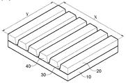
- FIG. 1 is a schematic model diagram illustrating a semiconductor device in accordance with some example embodiments of the inventive concepts.
- FIG. 2 is a graph measuring electrical characteristics of the semiconductor thin film ZnO before and after the scratch is formed (Comparative Examples 1 and 1).
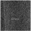
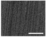
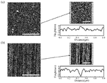
- FIG. 3 is an SEM image of a scratched semiconductor thin film ZnO. Scale bar represents 500 nm.
- FIG 4 is an AFM image of a substrate from which a scratched semiconductor thin film (ZnO) of the semiconductor device according to the present invention is removed.
- FIG. 5 is an AFM image illustrating a change in height of a semiconductor thin film ZnO as a scratch is formed on the semiconductor thin film.
- FIG. 6 is an image showing a change in bonding state between elements as a scratch is formed on a semiconductor thin film ZnO.
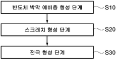
- FIG. 7 is a flow chart illustrating a method of manufacturing a sensor in accordance with example embodiments.
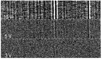
- FIG. 11 is an EFM image at 5V according to the film thickness of Example 1.
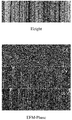
- FIG. 13 is an EFM image of Example 5.
- FIG. 14 is an XPS result showing changes in metal peaks and oxygen defect peaks of Comparative Example 1 and Example 1.
- FIG. 14 is an XPS result showing changes in metal peaks and oxygen defect peaks of Comparative Example 1 and Example 1.
- FIG. 15 is an XPS result showing changes in metal peaks and oxygen defect peaks of Comparative Examples 2 and 2.
- FIG. 15 is an XPS result showing changes in metal peaks and oxygen defect peaks of Comparative Examples 2 and 2.
- FIG. 16 is an XPS result showing changes in metal peaks and oxygen defect peaks of Comparative Examples 3 and 3.
- FIG. 16 is an XPS result showing changes in metal peaks and oxygen defect peaks of Comparative Examples 3 and 3.
- FIG. 17 is an XPS result showing changes in metal peaks and oxygen defect peaks of Comparative Examples 4 and 4.
- FIG. 17 is an XPS result showing changes in metal peaks and oxygen defect peaks of Comparative Examples 4 and 4.
- FIG. 18 is an XPS result showing changes in metal peaks of Comparative Examples 5 and 5.
- FIG. 18 is an XPS result showing changes in metal peaks of Comparative Examples 5 and 5.
- FIG. 19 is an SEM image of Comparative Example 1 and Comparative Example 2 and XPS results showing changes in metal peaks and oxygen defect peaks. Scale bars represent 2 ⁇ m.
- FIG. 20 compares the reaction of Comparative Example 1 and Example 1 with respect to 1000 ppm NO 2 gas.
- Example 22 is a comparison of the UV reaction of Comparative Example 1 and Example 1.
- Figure 23 shows the UV reaction of Comparative Example 6.
- FIG. 1 shows a schematic model diagram of a semiconductor device in accordance with example embodiments. 1, the width direction of the nanoribbon structure is represented by X, the length direction Y.
- a semiconductor device may include a substrate 10 and a semiconductor thin film 20 disposed on all or part of at least one surface of the substrate 10, and the semiconductor thin film 20 may be in at least a portion in one direction. It may include an array of nano ribbon structures 40.
- the substrate 10 supports the semiconductor thin film 20.
- the substrate 10 can support the semiconductor thin film 20.
- the substrate 10 commonly used in the art may be used without limitation.
- the substrate 10 may include a silicon (Si) wafer, a germanium (Ge) wafer, glass or an organic material.
- the organic material is polyimide (PI), polycarbonate (PC), polyether sulfone (PES), polyether ether ketone (PEEK), polybutylene terephthalate (PBT), polyethylene terephthalate (PET), polyvinyl chloride ( PVC), polyethylene (PE), ethylene copolymer, polypropylene (PP), propylene copolymer, poly (4-methyl-1-pentene) (TPX), polyarylate (PAR), polyacetal (POM), poly Phenylene oxide (PPO), polysulfone (PSF), polyphenylene sulfide (PPS), polyvinylidene chloride (PVDC), polyvinyl acetate (PVAC), polyvinyl alcohol (PVAL), polyvinyl acetal, polystyrene (PS ), AS resin, ABS resin, polymethyl methacrylate (PMMA), fluorine resin, phenol resin (PF), melamine resin (MF), urea resin (UF), uns
- the substrate 10 may include one or more functional groups selected from the group consisting of a hydroxy group, a thiol group, and a perfluoroalkyl group formed on one surface.
- the functional groups may interact with the metal atoms to form a uniform conductive metal thin film that does not include grain-boundaries.
- the functional group may interact with metal atoms of the metal film located on the graphene layer to form an ultraconductive metal thin film on the substrate 10.
- the substrate 10 including a thiol group or a perfluoroalkyl group on one side may be used as a mercaptoalkylalkoxysilane or a perfluoroalkylalkoxysilane, respectively.
- the mercaptoalkylalkoxysilane may include (3-mercaptopropyl) trimethoxysilane.
- the perfluoroalkylalkoxysilane may include 1H, 1H, 2H, 2H-perfluorooctyltriethoxysilane (1H, 1H, 2H, 2H-perfluorooctyltriethoxysilane).
- the thickness of the substrate 10 may be 0.1 ⁇ m to 1000 ⁇ m.
- the semiconductor thin film 20 may be disposed on the surface of the substrate 10.
- the semiconductor thin film 20 may be disposed on at least a portion of at least one surface of the substrate 10.
- At least one surface of the thin film 20 may be a plurality of continuous surfaces or a plurality of non-continuous surfaces.
- the range and portion in which the semiconductor thin film 20 is disposed on the substrate 10 are not particularly limited.
- the semiconductor thin film 20 may include a nanoribbon structure 40 arranged in at least a portion in one direction.
- the nanoribbon structure 40 may include a strip-shaped structure in which the width of the unit nanoribbon structure in the X direction is several to several hundred nanometers.
- the nanoribbon structure may be formed by contacting the surface of the semiconductor thin film with particles of greater strength than the semiconductor thin film 40 to form the scratch 30 in one direction.
- the electric conductivity value in the longitudinal direction Y of the scratch may be at least two times, at least five times, or at least ten times the conductivity value in the width direction X perpendicular thereto.
- the upper limit is not limited because the resistance value in the X direction may be near infinity, and may be, for example, 20 times the value in the Y direction.
- the semiconductor thin film 20 may have improved semiconductor characteristics as the nanoribbon structure 40 is formed by the scratch 30.
- FIG. 2 is a graph measuring the drain current with respect to the gate voltage and the drain voltage before and after the scratch is formed on the semiconductor thin film ZnO (Comparative Examples 1 and 1). Referring to FIG. 2, when the scratch 30 is formed in one direction (FIG. 2C and FIG. 2D) in the thin film 20, the scratch 30 is not formed (FIG. 2). It can be seen that the semiconductor characteristics are improved from (a)).
- the improvement of semiconductor characteristics as the scratch 30 is formed may be due to the formation of independent nanoribbon structures 40 arranged in one direction in the semiconductor thin film.
- a semiconductor device may include a semiconductor thin film 20 having a scratch 30 formed in one direction.
- FIG. 4 is an AFM image of the substrate 10 taken after nitric acid is removed from the semiconductor thin film 20 in which the scratches 30 are formed in one direction of the semiconductor device according to example embodiments.
- scratches may be present on the substrate 10 from which the semiconductor thin film 20 is removed.
- the scratch present on the substrate 10 may be formed as the scratch 30 is deep enough to reach the substrate in the process of forming the scratch 30 in the semiconductor thin film 20.
- an independent nanoribbon structure 40 may be formed between adjacent scratches 30 formed in one direction. Accordingly, semiconductor characteristics of the semiconductor device may be improved.
- FIG. 5 is an AFM image illustrating a change in height of a semiconductor thin film ZnO as a scratch is formed on the semiconductor thin film.
- a distance 0 nm to 400 nm section may be a semiconductor thin film on which the nanoribbon structure 40 is formed due to scratching, and a 400 nm to 800 nm section represents a portion of the substrate on which scratches are formed.
- the thickness of the remaining semiconductor thin film after the scratch is formed may be about 10 nm to 18 nm. As shown in FIG. 4, the scratch is made deep enough to reach the substrate so that the thickness of the semiconductor thin film of the scratched portion may be substantially close to zero. In this case, independent nanoribbon structures 40 may be formed between the scratches 30 adjacent to each other. Accordingly. The semiconductor characteristics of the semiconductor device can be further improved.
- the semiconductor thin film 20 may be a semiconductor thin film conventionally used in the art without limitation, for example, a metal oxide semiconductor thin film, a silicon semiconductor thin film, a gallium arsenide semiconductor thin film, a germanium-semiconductor thin film, a silicon-germanium semiconductor thin film, and the like. It may include at least one selected from the group consisting of an organic semiconductor thin film.
- the organic semiconductor thin film may be an organic semiconductor thin film commonly used in the art without limitation, and may include, for example, a pentacene thin film.
- the metal oxide semiconductor thin film may be any metal oxide semiconductor thin film conventionally used in the art, for example, ZnO, MgO, SrO, TiO 2 , SnO 2 , In 2 O 3, and Ga 2 O 3 . It may include any one selected from the group.
- the semiconductor thin film 30 may include a metal oxide semiconductor thin film.
- the metal peak and oxygen defect peak of the XPS spectrum do not have the scratch 30. May be increased.
- metal peaks and oxygen defect peaks in the XPS spectrum are observed. Can be increased.
- the physical change may be a change in surface area and shape of the surface of the thin film as scratches are formed in the semiconductor thin film.
- the chemical change may be the formation of metal dimers between metal atoms as the bond between the metal atoms and the oxygen atoms is broken.
- FIG. 6 is an image showing chemical change of a semiconductor thin film ZnO as a scratch is formed.
- the left side is an image of the ZnO thin film before the scratch is formed
- the right side is an image of the ZnO thin film in which the oxygen defect occurs after the scratch is formed.
- oxygen defects may occur, and Zn-Zn dimers may be formed at the positions.
- the thickness of the semiconductor thin film 20 may be about 10 nm to 500 ⁇ m.
- the thickness of the thin film is less than about 10 nm, the semiconductor thin film is entirely cut off during the process of forming the scratch 30, and the nano ribbon structure 40 cannot be formed.
- the thickness of the thin film exceeds about 500 ⁇ m, the independent nano ribbon structure (40 ), It may be difficult to expect improved semiconductor properties.
- the width of the nanoribbon structure 40 formed on the surface of the semiconductor thin film 20 may be about 10nm to 250nm.
- the width of the nanoribbon structure 40 formed on the surface of the semiconductor thin film 20 is 10 nm to 250 nm, the sensitivity of the sensor including the semiconductor element is improved, and the operating temperature is lowered to reduce power consumption.
- the width of the nanoribbon structure 40 is less than about 10 nm, it may be difficult to form the nanoribbon structure, and it may be difficult to expect excellent semiconductor properties, and if the width of the nanoribbon structure 40 exceeds about 250 nm, As the density of the nanoribbon structure 40 decreases, it may be difficult to expect good semiconductor properties.
- the depth of the scratch 30 formed on the surface of the semiconductor thin film 20 may be equal to or greater than the thickness of the semiconductor thin film 20.
- the nanoribbon structure 40 may be more easily formed on the surface of the semiconductor thin film 20. Accordingly, the sensitivity of the sensor including the semiconductor element is excellent and the operating temperature is lowered, thereby reducing power consumption.
- the depth of the scratch 30 may be about 0.5 nm to 100 nm, but is not limited thereto.
- the depth when the depth is less than about 0.5 nm, the physical chemical change of the surface of the semiconductor thin film may not occur sufficiently, so that the sensitivity of the sensor including the semiconductor device may be reduced.
- the upper limit of the depth of the scratch 30 is not a problem, but may be as deep as, for example, the thickness of the semiconductor thin film.
- the substrate may be a depth at which leakage current does not occur in the substrate supporting the semiconductor thin film.
- a method of manufacturing a semiconductor device may include forming a semiconductor thin film preliminary layer (S10); And forming a scratch (S20).
- a semiconductor thin film preliminary layer may be formed on a substrate (S10).
- the method for forming the semiconductor thin film preliminary layer may be a method of forming a thin film commonly used in the art, and examples thereof include chemical vapor deposition (CVD), physical vapor deposition (PVD), atomic layer deposition (ALD), sol-gel method and the like can be used.
- CVD chemical vapor deposition
- PVD physical vapor deposition
- ALD atomic layer deposition
- sol-gel method sol-gel method and the like
- the particles having greater strength than the semiconductor thin film preliminary layer may be brought into contact with the surface of the semiconductor thin film preliminary layer to form scratches in one direction (S20).
- Particles having a greater strength than the semiconductor thin film preliminary layer may be used without limitation as long as the particles have greater strength in consideration of the kind of the semiconductor thin film preliminary layer.
- the particle may be a diamond particle.
- the size of the particles having greater strength than the semiconductor thin film preliminary layer may be changed according to the width and depth of the scratch to be formed. However, the particle size may be uniform to form a scratch of a certain size.
- the average particle diameter (D50) of the particles having higher strength than the semiconductor thin film may be about 0.5 to 10 ⁇ m.
- the average particle diameter (D50) of the particles having higher strength than the semiconductor thin film is less than about 0.5 ⁇ m, scratches of sufficient depth cannot be formed, and thus, it is difficult to form the independent nanoribbon structure 40, and the average particle diameter of the particles
- the D50 exceeds about 10 ⁇ m, the width and depth of the scratch 30 may be excessively large, and thus the density of the ribbon structure 40 may be reduced. Accordingly, semiconductor characteristics of the semiconductor device may be degraded, and sensitivity of the sensor including the semiconductor device may be reduced.
- the scratch may be formed by moving a particle having a greater strength than the semiconductor thin film in a predetermined direction while contacting the surface of the semiconductor thin film.
- the movement method for scratch formation is not particularly limited as long as the scratch is formed in a certain direction, for example, the formation direction of the scratch may be a circle, an ellipse, a straight line or a curved direction.
- a semiconductor thin film including a nanoribbon structure arranged in one direction may be obtained.
- the method of manufacturing a semiconductor device may further include an electrode forming step (S30).
- the forming of the electrode may deposit a metal to be used as an electrode on the scratch formed thin film.
- the metal deposition method may be used without limitation metal deposition methods commonly used in the art, for example, chemical vapor deposition (CVD), physical vapor deposition (PVD) or atomic layer deposition (ALD), etc. This can be used.
- CVD chemical vapor deposition
- PVD physical vapor deposition
- ALD atomic layer deposition
- the metal deposited according to the deposition method may be used without limitation, metals commonly used in the art, for example, a metal such as gold, platinum, aluminum, copper or iron may be selected.
- the semiconductor device may be usefully used for a sensor, and the sensor according to some exemplary embodiments may be used as a gas or ultraviolet sensing sensor.
- the gas may comprise NH 3 , NO 2 , NO, CO or H 2 .
- Step 1 Form a ZnO Thin Film
- a 20 nm thick ZnO thin film was deposited on a silicon substrate (650 ⁇ m) on which a 500 nm thick oxide film was deposited using an ALD process.
- the ALD process reacts diethyl zinc (DEZ) vapor with the substrate surface to form a zinc layer, purge step to remove unreacted diethyl zinc (DEZ) using purge gas, and applies oxygen atoms by applying H 2 O pulses.
- DEZ diethyl zinc
- purge step to remove unreacted diethyl zinc (DEZ) using purge gas
- oxygen atoms by applying H 2 O pulses.
- One cycle followed by 100 cycles of adhesion.
- Step 2 scratch formation of the ZnO thin film
- the scratch process used a grinding / polishing machine. After sufficiently moistening the cloth to be used for polishing, a polycrystalline diamond powder solution (Allied High Tech, 90-32015) having an average particle diameter (D50) of 1 ⁇ m was sprayed onto the cloth. After spinning lightly to distribute the diamond powder evenly on the cloth, the silicon substrate on which the semiconductor thin film (ZnO) was deposited was lightly pressed for three seconds so that the ZnO surface was in contact with the cloth. The polished substrate was washed with ultrasonic waves in the order of acetone, isopropyl alcohol (IPA) solution, and deionize water to remove the residue.
- IPA isopropyl alcohol
- An electrode was formed on the scratch-formed semiconductor thin film and manufactured as a sensor element.
- the electrode was manufactured by depositing Al by thermal deposition using a stencil mask.
- Example 2 It was manufactured in the same manner as in Example 1 except that an In 2 O 3 thin film was formed on the substrate instead of the ZnO thin film.
- Example 2 Instead of forming a ZnO thin film by the ALD process on the substrate was produced in the same manner as in Example 1 except that TiO 2 is formed by using a sputter.
- Example 2 It was manufactured in the same manner as in Example 1 except that a SnO 2 thin film was formed on the substrate instead of a ZnO thin film.
- Comparative Example 1 was manufactured in the same manner as in Comparative Example 1 except that the ALD process was performed on the filter paper other than the silicon substrate.
- Example 1 In order to identify the cause of the outstanding scratch effect, the drain voltage of the semiconductor device according to Comparative Example 1 and Example 1 and the drain current according to the gate voltage was specified and compared in FIG. 2.
- Comparative Example 1 the ZnO thin film is almost metallic, whereas Example 1 exhibits distinct semiconductor characteristics.
- FIG. 3 it can be seen that scratches of nanometer depth are formed in a predetermined direction on the entire surface of the semiconductor thin film of Example 1.
- FIG. 3 it can be seen that scratches of nanometer depth are formed in a predetermined direction on the entire surface of the semiconductor thin film of Example 1.
- Example 1 An AFM image of a substrate taken after removing a semiconductor thin film on which a scratch formed on a substrate is removed with nitric acid in Example 1 is shown in FIG. 4.
- the scratch is formed deeper than the thickness of the semiconductor thin film. Accordingly, it can be seen that the scratch formed on the semiconductor thin film penetrates the thin film and nanoribbons the thin film.
- FIG. 5 A graph showing the AFM image and the height difference of the semiconductor device of Example 1 is shown in FIG. 5.
- a distance of 0 to 400 nm represents a unit nano ribbon structure on which scratches are formed
- a distance of 400 nm to 800 nm represents a substrate.
- the height of the thin film after scratch corresponds to about 15 nm.
- FIGS. 8 to 10 shows the AFM observation image of Example 1.
- FIG. 9 (a) shows an AFM observation image of Comparative Example 2
- FIG. 9 (b) shows an AFM observation image of Example 2.
- FIG. 10 (a) shows an AFM observation image of Comparative Example 4
- FIG. 10 (b) shows an AFM observation image of Example 4.
- scratches are formed on the entire surface of the semiconductor thin film with a nanometer depth in a predetermined direction. It was also confirmed that the width of the formed scratch was 10 nm to 250 nm, and the depth was 0.5 nm or more.
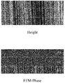
- FIGS. 11 to 13 are EFM observation images of Examples 1, 3, and 5 are shown in FIGS. 11 to 13.
- 11 is an EFM observation image of Example 1
- FIG. 12 is an EFM observation image of Example 3
- FIG. 13 is an EFM observation image of Example 5.
- a nanometer-depth scratch was formed in the entire direction of the surface of the semiconductor thin film, and the surface potential of the scratched portion appeared to increase when an electric field was applied, and this phenomenon was increased at 5V or higher.
- Comparative Examples 1 to 5 and Examples 1 to 5 were analyzed by XPS and shown in FIGS. 14 to 18.
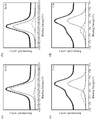
- FIG. 14 is an XPS result showing changes in oxygen defect peaks and metal peaks of Comparative Example 1 and Example 1.
- FIG. 14 is an XPS result showing changes in oxygen defect peaks and metal peaks of Comparative Example 1 and Example 1.
- Example 1 with scratches are shown in Figs. 14 (b) and (d), and the results of Comparative Example 1 with no scratches are shown in Figs. 14 (a) and (c), respectively.
- peaks 1021.1 eV of the metallic Zn of Comparative Example 1 and Example 1 are indicated by double-dotted lines in FIGS. 14A and 14B, respectively.
- the oxygen defect peaks 531.4 eV of Comparative Example 1 and Example 1 are shown by double-dotted lines in Figs. 14 (c) and 14 (d), respectively.
- the dashed line in FIG. 14 (b) showing the metallic Zn peak (1021.1 eV) in Example 1 has a peak higher than the dashed line in FIG. 14 (a) showing the metallic Zn peak (1021.1 eV) in Comparative Example 1. Increased.
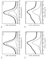
- FIG. 15 is an XPS result showing changes in oxygen defect peaks and metal peaks of Comparative Examples 2 and 2.
- FIG. 15 is an XPS result showing changes in oxygen defect peaks and metal peaks of Comparative Examples 2 and 2.
- Example 2 with scratches are shown in FIGS. 15B and 15D, and the results of Comparative Example 2 without scratches are shown in FIGS. 15A and 15C, respectively.
- FIG. 15 the peaks of the metallic Zn (1021.1 eV) of Comparative Example 2 and Example 2 are shown by double-dotted lines in FIGS. 15A and 15B, respectively.
- Oxygen defect peaks 532 eV of Comparative Example 2 and Example 2 are shown by double-dotted lines in Figs. 15 (c) and (d), respectively.
- the dashed line in FIG. 15 (b) showing the metallic Zn peak (1021.1 eV) in Example 2 has a higher peak than the dashed line in FIG. 15 (a) showing the metallic Zn peak (1021.1 eV) in Comparative Example 2. Increased.
- FIG. 15 (d) showing the oxygen defect peak 532eV of Example 2 has a higher peak than the dashed-dotted line of FIG. 15 (c) which shows the oxygen defect peak 532eV of Comparative Example 2.
- FIG. 15 (c) which shows the oxygen defect peak 532eV of Comparative Example 2.
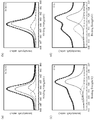
- FIG. 16 is an XPS result showing changes in oxygen defect peaks and metal peaks of Comparative Examples 3 and 3.
- FIG. 16 is an XPS result showing changes in oxygen defect peaks and metal peaks of Comparative Examples 3 and 3.
- Example 3 with scratches are shown in FIGS. 16B and 16D, and the results of Comparative Example 3 with no scratches are shown in FIGS. 16A and 16C, respectively.
- the peaks (444 eV) of the metallic In of Comparative Example 3 and Example 3 are shown by dashed lines in FIGS. 16A and 16B, respectively.
- the oxygen defect peak 531 eV of the comparative example 3 and Example 3 is shown with the dotted line in FIG.16 (c), (d), respectively.
- FIG. 16 (d) showing the oxygen defect peak 531eV of Example 3 has a higher peak than the dotted line of FIG. 16 (c) showing the oxygen defect peak 531eV of Comparative Example 3.
- FIG. 16 (d) showing the oxygen defect peak 531eV of Example 3 has a higher peak than the dotted line of FIG. 16 (c) showing the oxygen defect peak 531eV of Comparative Example 3.
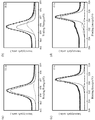
- FIG. 17 is an XPS result showing changes in oxygen defect peaks and metal peaks of Comparative Examples 4 and 4.
- FIG. 17 is an XPS result showing changes in oxygen defect peaks and metal peaks of Comparative Examples 4 and 4.
- Example 4 with scratches are shown in FIGS. 17B and 17D, and the results of Comparative Example 4 with no scratches are shown in FIGS. 17A and 17C, respectively.
- peaks (437.8 eV) of the metallic Tis of Comparative Example 4 and Example 4 are shown as dotted lines in FIGS. 17A and 17B, respectively.
- oxygen defect peaks 531.1 eV of Comparative Example 4 and Example 4 are shown by dotted lines in Figs. 17 (c) and 17 (d), respectively.
- the dotted line of FIG. 17 (b) showing the metallic Ti peak (437.8eV) of Example 4 has a higher peak than the dotted line of FIG. 17 (a) showing the metallic Ti peak (1021.1 eV) of Comparative Example 4. .
- the dotted line of FIG. 17 (d) showing the oxygen defect peak (531.1 eV) of Example 4 has a higher peak than the dotted line of FIG. 17 (c) showing the oxygen defect peak (531.1 eV) of Comparative Example 4.
- FIG. 18 is an XPS result showing changes in metal peaks of Comparative Examples 5 and 5.
- FIG. 18 is an XPS result showing changes in metal peaks of Comparative Examples 5 and 5.
- Example 5 with scratches are shown in FIG. 18 (b), and the results of Comparative Example 5 with no scratches are shown in FIG. 18 (a).
- FIG. 18 the peaks (485.7 eV) of the metallic Sns of Comparative Examples 5 and 5 are shown in dashed lines in FIGS. 18A and 18B, respectively.
- the dotted line of FIG. 18 (b) showing the metallic Sn peak (485.7eV) of Example 5 has a higher peak than the dotted line of FIG. 18 (a) showing the metallic Sn peak (485.7eV) of Comparative Example 5. .
- ZnO powder was hydrothermally synthesized on the substrate. Step 3 of Example 1 was performed to form an electrode.
- ZnO powder was prepared in Comparative Example 1 hydrothermally synthesized and prepared in the same manner as in Comparative Example 1 except that the powder was ground with a mortar before forming the electrode.
- FIG. 19 is an XPS result and SEM image showing changes in metal peaks and oxygen defect peaks of Comparative Examples 1 and 2.
- FIG. 19 is an XPS result and SEM image showing changes in metal peaks and oxygen defect peaks of Comparative Examples 1 and 2.
- FIG. 19 the peaks of the metallic Zn (1021.1 eV) of Comparative Example 1 and Comparative Example 2 are shown in dashed lines in FIGS. 19A and 19B, respectively.
- peaks (531.4 eV) of oxygen defects of Comparative Example 1 and Comparative Example 2 are indicated by double-dotted lines in Figs. 19 (c) and (d), respectively.
- FIG. 19 (d) showing the oxygen defect peak (531.4 eV) of the comparative example 2 was similar in peak to the dotted line in FIG. 19 (c) showing the oxygen defect peak (531.4 eV) of the comparative example 1.
- FIG. 19 (d) showing the oxygen defect peak (531.4 eV) of the comparative example 2 was similar in peak to the dotted line in FIG. 19 (c) showing the oxygen defect peak (531.4 eV) of the comparative example 1.
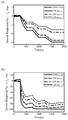
- FIG. 20 is a comparison of the reaction of 1000 ppm NO 2 gas of Comparative Example 1 and Example 1, FIG. 20 (a) shows the reaction of 1000 ppm NO 2 gas of Comparative Example 1, FIG. 20 (b) The reaction with 1000 ppm NO 2 gas of Example 1 is shown.
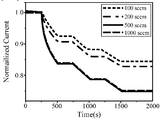
- FIG. 21 shows a reaction with a 1000 ppm NO 2 gas of Comparative Example 6.
- Example 1 showed a sensitivity and a short reaction time more than 100 times compared to Comparative Example 1 which is a general thin film
- Example 1 showed excellent sensitivity and a short reaction time of 100 times or more, compared with Comparative Example 6, which maximized the surface area.
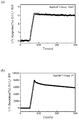
- FIG 22 is a comparison of the reaction to UV of Comparative Example 1 and Example 1 in Figure 22 (a) shows a response to the UV of Comparative Example 1, Figure 22 (b) for the UV of Example 1 The reaction was shown.
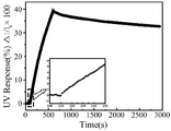
- Figure 23 shows the response to the UV of Comparative Example 6.
- Example 1 showed a sensitivity of 100 times or more and a very short reaction time compared to Comparative Example 1 which is a general thin film.
- Example 1 showed a sensitivity of 200 times or more and a very short reaction time even in comparison with Comparative Example 6, which maximized the surface area.
Landscapes
- Chemical & Material Sciences (AREA)
- General Health & Medical Sciences (AREA)
- Pathology (AREA)
- Physics & Mathematics (AREA)
- Health & Medical Sciences (AREA)
- Life Sciences & Earth Sciences (AREA)
- Analytical Chemistry (AREA)
- Electrochemistry (AREA)
- General Physics & Mathematics (AREA)
- Biochemistry (AREA)
- Immunology (AREA)
- Chemical Kinetics & Catalysis (AREA)
- Engineering & Computer Science (AREA)
- Nanotechnology (AREA)
- Thin Film Transistor (AREA)
- Materials Engineering (AREA)
Description
본 발명은 반도체 소자, 이의 제조 방법 및 이를 포함하는 센서에 관한 것이다. 보다 상세하게는, 반도체 박막을 포함하는 반도체 소자, 이의 제조 방법, 및 이를 포함하는 센서에 관한 것이다.
최근 기술 발전에 따라 다양한 센서들이 연구 및 개발되고 있다. 특히, IoT 발전에 따라 전기적 신호를 송출하는 센서타입인 전기화학식 센서와 반도체 방식의 센서가 유용할 것으로 판단되고 있다.
반도체 방식의 센서는 마이크로미터 이하로 작은 센서의 제작 및 집적화가 가능한 장점을 가지고 있으나, 대부분 산화물 반도체 박막으로 이루어져, 센서 소재의 선택성과 감도가 불량하고, 고온에서 작동하므로 소비전력이 큰 취약점을 갖는다.
이와 같은 문제를 해결하기 위하여 센서소재로 각종 나노물질이 적용되어 왔다. 바텀업(bottomup) 소재로는 탄소 나노튜브, 반도체 나노선등의 1차원 나노물질 등이 있으며, 탑다운(topdown) 소재로는 식각된 나노선 등 이 있다. 그러나, 바텀업 소재의 경우, 나노 소재의 균일성/안정성 문제 때문에, 탑다운 방식의 경우 나노 리소그래피가 필요하기 때문에 사업화가 어려운 실정이다. 이에 따라, 높은 감도와 양호한 소비전력을 가지면서 동시에 공정비용을 낮출 수 있는 새로운 기술이 필요하다.
한편, 한국등록특허공보 제10-2008-0094741호(2008.09.26)는 박막형 센싱부재를 이용한 화학센서에 관한 발명으로, 제1전극 및 제2전극 사이의 박막형 센싱부재를 구비한다. 박막형 센싱부재는 화학센서에서의 면적이 넓어서 화학 센서의 감도가 향상되며, 제2전극은 나노구조체로서 센싱부재의 표면을 노출시킬 수 있다. 이를 통해 감도가 향상된 화학 센서를 제공한다.
본 발명의 일 과제는 간단하게 제조될 수 있는 반도체 소자 및 이를 포함하는 센서를 제공하는 것이다.
본 발명의 일 과제는 감도 및 전기적 특성이 개선된 센서를 제공하는 것이다.
1. 기재; 및 상기 기재의 적어도 일면의 전부 또는 일부에 배치된 반도체 박막을 포함하며, 상기 반도체 박막은 적어도 일부에 일 방향으로 배열된 나노 리본 구조를 포함하는 반도체 소자.
2. 위 1에 있어서, 상기 나노 리본 구조는 상기 반도체 박막 보다 강도가 큰 입자를 상기 반도체 박막의 표면과 접촉시켜 일 방향으로 스크래치를 형성함에 따라 형성된, 반도체 소자.
3. 위 1에 있어서, 상기 반도체 박막은 금속산화물 반도체 박막, 실리콘 반도체 박막, 갈륨비소 반도체 박막, 게르마늄-반도체 박막, 실리콘-게르마늄 반도체 박막 및 유기반도체 박막로 이루어진 군에서 선택된 적어도 하나를 포함하는, 반도체 소자.
4. 위 1에 있어서, 상기 반도체 박막은 금속산화물 반도체 박막인 반도체 소자.
5. 위 4에 있어서, 상기 금속산화물 반도체 박막은 ZnO, MgO, SrO, TiO
2, SnO
2, In
2O
3 및 Ga
2O
3로 이루어진 군에서 선택된 어느 하나를 포함하는 박막인 반도체 소자.
6. 위 4에 있어서, 상기 금속산화물 반도체 박막은 XPS 스펙트럼의 금속 피크 및 산소 결함 피크가 스크래치가 형성되지 않은 반도체 박막보다 증가된 것인 반도체 소자.
7. 위 1에 있어서, 상기 반도체 박막은 그 두께가 10nm 내지 500㎛인 반도체 소자.
8. 위 2에 있어서, 상기 나노 리본 구조의 폭은 10nm 내지 250nm이고, 상기 스크래치의 깊이는 상기 반도체 박막의 두께보다 깊거나 같은, 반도체 소자.
9. (S10) 기재 상에 반도체 박막 예비층을 형성하는 단계; 및 (S20) 상기 반도체 박막 예비층보다 강도가 큰 입자를 상기 반도체 박막 예비층의 표면과 접촉시켜 일 방향으로 스크래치를 형성하는 단계를 포함하는 반도체 소자의 제조방법.
10. 위 9에 있어서, 상기 입자는 다이아몬드 입자인 반도체 소자의 제조방법.
11. 위 9에 있어서, 상기 입자는 평균 입경(D50)이 1 내지 10 ㎛인 반도체 소자의 제조방법.
12. 위 1의 반도체 소자를 포함하는 센서.
본 발명의 예시적 실시예들에 따라 제조된 반도체 소자는 반도체 박막의 물리적 구조 및 화학적 특성이 변화되어 그를 포함하는 센서의 감도가 향상될 수 있다.
본 발명의 예시적 실시예들에 따라 제조된 반도체 소자는 그 제조방법이 간단하여, 공정 시간 및 비용을 감축할 수 있다.
본 발명의 예시적 실시예들에 따라 제조된 반도체 소자는 나노 크기를 가져, 그를 포함하는 센서의 작동온도 및 소비전력이 감소될 수 있다.
도 1은 본 발명의 예시적인 실시예들에 따른 반도체 소자를 나타내는 개략적인 모형도이다.
도 2는 반도체 박막(ZnO)에 스크래치가 형성되기 전 후(비교예 1 및 실시예 1)의 전기적 특성을 측정한 그래프이다.
도 3은 스크래치가 형성된 반도체 박막(ZnO)의 SEM 이미지이다. 스케일바(scale bar)는 500nm를 나타낸다.
도 4는 본 발명에 따른 반도체 소자의 스크래치가 형성된 반도체 박막(ZnO)을 제거한 기판의 AFM 이미지이다.
도 5는 반도체 박막에 스크래치가 형성됨에 따른 반도체 박막(ZnO)의 높이 변화를 나타내는 AFM 이미지이다.
도 6은 반도체 박막(ZnO)에 스크래치가 형성됨에 따른 원소간 결합 상태의 변화를 보여주는 이미지이다.
도 7는 예시적인 실시예들에 따른 센서의 제조 방법을 나타내는 순서도이다.
도 8은 스크래치가 형성된 반도체 박막(ZnO)의 AFM 이미지이다. 스케일바(scale bar)는 3 ㎛를 나타낸다.
도 9은 비교예 2 및 실시예 2의 AFM 이미지이다. 스케일바(scale bar)는 3 ㎛를 나타낸다.
도 10은 비교예 4 및 실시예 4의 AFM 이미지이다.
도 11은 실시예 1의 박막 두께에 따른 5V에서의 EFM 이미지이다.
도 12은 실시예 3의 EFM 이미지이다.
도 13은 실시예 5의 EFM 이미지이다.
도 14는 비교예 1과 실시예 1의 금속 피크(metal peak) 및 산소 결함 피크(oxygen defect peak)의 변화를 보여주는 XPS 결과이다.
도 15은 비교예 2와 실시예 2의 금속 피크(metal peak) 및 산소 결함 피크(oxygen defect peak)의 변화를 보여주는 XPS 결과이다.
도 16는 비교예 3과 실시예 3의 금속 피크(metal peak) 및 산소 결함 피크(oxygen defect peak)의 변화를 보여주는 XPS 결과이다.
도 17는 비교예 4와 실시예 4의 금속 피크(metal peak) 및 산소 결함 피크(oxygen defect peak)의 변화를 보여주는 XPS 결과이다.
도 18은 비교예 5와 실시예 5의 금속 피크(metal peak)의 변화를 보여주는 XPS 결과이다.
도 19은 대조예 1과 대조예 2의 SEM 이미지 결과 및 금속 피크(metal peak)와 산소 결함 피크(oxygen defect peak)의 변화를 보여주는 XPS 결과이다. 스케일바(scale bar)는 2㎛를 나타낸다.
도 20은 비교예 1과 실시예 1의 1000ppm NO2 가스에 대한 반응을 비교한 것이다.
도 21는 비교예 6의 1000ppm NO2 가스에 대한 반응을 나타낸 것이다.
도 22은 비교예 1과 실시예 1의 UV 반응을 비교한 것이다.
도 23은 비교예 6의 UV 반응을 나타낸 것이다.
도 24은 각 기체가 스크래치가 형성된 ZnO 표면과 결합하는 모습을 보여주는 이미지이다.
이하, 첨부한 도면들을 참조하여 본 발명을 상세히 설명하기로 한다. 하기에서 본 발명의 바람직한 일 실시예를 제시하나, 하기 실시예는 본 발명을 예시하는 것일 뿐 첨부된 특허청구범위를 제한하는 것이 아니며, 본 발명의 범주 및 기술사상 범위 내에서 하기 실시예에 대한 다양한 변경 및 수정이 가능함은 당업자에게 있어서 명백한 것이며, 이러한 변형 및 수정이 첨부된 특허청구범위에 속하는 것도 당연한 것이다.
도 1은 예시적인 실시예들에 따른 반도체 소자의 개략적인 모형도를 나타낸다. 도 1은 나노 리본 구조의 폭 방향을 X, 길이 방향을 Y로 표시하였다.
예시적인 실시예들에 따른 반도체 소자는 기재(10) 및 기재(10)의 적어도 일면의 전부 또는 일부에 배치된 반도체 박막(20)을 포함하며, 반도체 박막(20)은 적어도 일부에 일 방향으로 배열된 나노 리본 구조(40)를 포함할 수 있다.
기재(10)는 반도체 박막(20)을 지지한다. 기재(10)는 반도체 박막(20)을 지지할 수 있는 것이라면 당 분야에서 통상적으로 사용되는 기재(10)가 제한 없이 사용될 수 있다. 예를 들면, 기재(10)는 실리콘(Si) 웨이퍼, 게르마늄(Ge) 웨이퍼, 유리 또는 유기물 등을 포함할 수 있다.
상기 유기물은 폴리이미드(PI), 폴리카보네이트(PC), 폴리에테르설폰(PES), 폴리에테르에테르케톤(PEEK), 폴리부틸렌테레프탈레이트(PBT), 폴리에틸렌테레프탈레이트(PET), 폴리염화비닐(PVC), 폴리에틸렌(PE), 에틸렌 공중합체, 폴리프로필렌(PP), 프로필렌 공중합체, 폴리(4-메틸-1-펜텐)(TPX), 폴리아릴레이트(PAR), 폴리아세탈(POM), 폴리페닐렌옥사이드(PPO), 폴리설폰(PSF), 폴리페닐렌설파이드(PPS), 폴리염화비닐리덴(PVDC), 폴리초산비닐(PVAC), 폴리비닐알콜(PVAL), 폴리비닐아세탈, 폴리스티렌(PS), AS수지, ABS수지, 폴리메틸메타크릴레이트(PMMA), 불소수지, 페놀수지(PF), 멜라민수지(MF), 우레아수지(UF), 불포화폴리에스테르(UP), 에폭시수지(EP), 디알릴프탈레이트수지(DAP), 폴리우레탄(PUR), 폴리아미드(PA) 및 실리콘수지(SI) 중 적어도 어느 하나를 포함할 수 있다.
기재(10)는 일면에 형성된 히드록시기, 티올기 및 퍼플루오로알킬기로 이루어진 군에서 선택된 하나 이상의 작용기를 포함할 수 있다. 이 경우, 상기 작용기가 금속 원자와 상호 작용하여 결정립계(grain-boundaries)를 포함하지 않은 균일한 전도성 금속 박막을 형성할 수 있다.
예를 들면, 상기 작용기는 그래핀층 상에 위치한 금속막의 금속 원자와 상호 작용하여, 기재(10) 상에 전도성 금속 초박막의 형성할 수도 있다.
예를 들면, 일면 상에 티올기 또는 퍼플루오로알킬기를 포함하는 기재(10)는 히드록시기를 포함하는 기재(10)를 각각 머캅토알킬알콕시실란(mercaptoalkylalkoxysilane) 또는 퍼플루오로알킬알콕시실란(perfluoroalkylalkoxysilane)으로 처리하여 제조될 수 있다.
예를 들면 상기 머캅토알킬알콕시실란(mercaptoalkylalkoxysilane)은 (3-머캅토프로필)트리메톡시실란((3-mercaptopropyl)trimethoxysilane)을 포함할 수 있다. 예를 들면, 상기 퍼플루오로알킬알콕시실란(perfluoroalkylalkoxysilane)은 1H,1H,2H,2H-퍼플루오로옥틸트리에톡시실란(1H,1H,2H,2H-perfluorooctyltriethoxysilane)을 포함할 수 있다.
예를 들면, 기재(10)의 두께는 0.1㎛ 내지 1000㎛일 수 있다.
반도체 박막(20)은 기재(10)의 표면에 배치 될 수 있다. 예를 들면 반도체 박막(20)은 기재(10)의 적어도 일면 상의 적어도 일부에 배치될 수 있다. 상기 박막(20) 적어도 일면은 연속된 복수의 면 또는 연속되지 않은 복수의 면일 수 있다. 기재(10) 상에 반도체 박막(20)이 배치되는 범위 및 부분은 특별한 제한이 없다.
반도체 박막(20)은 적어도 일부에 일 방향으로 배열된 나노 리본 구조(40)를 포함할 수 있다. 예를 들면, 나노 리본 구조(40)는 단위 나노 리본 구조의 X방향의 폭이 수 내지 수백 나노미터 수준인 띠 모양의 구조를 포함할 수 있다.
일부 예시적인 실시예들에 있어서, 나노 리본 구조는(40) 반도체 박막 보다 강도가 큰 입자를 상기 반도체 박막의 표면과 접촉시켜 일 방향으로 스크래치(30)를 형성함에 따라 형성될 수 있다.
일부 예시적인 실시예들에 따른 반도체 소자는 스크래치의 길이 방향(Y)의 전기전도도 값이 이와 수직한 폭 방향(X)의 전기전도도 값의 2배 이상, 5배 이상, 또는 10배 이상일 수 있다. 실질적으로는 X 방향의 저항 값이 무한대에 가까울 수 있으므로 그 상한은 한정하지는 않으며 예를 들면, Y 방향 저항 값의 20배 일 수도 있다.
반도체 박막(20)은 스크래치(30)에 의해 나노 리본 구조(40)가 형성됨에 따라 향상된 반도체 특성을 가질 수 있다.
도 2는 반도체 박막(ZnO)에 스크래치가 형성되기 전 후(비교예 1 및 실시예 1)의 게이트 전압 및 드레인 전압에 대한 드레인 전류를 측정한 그래프이다. 도 2를 참조하면, 박도체 박막(20)에 일 방향으로 스크래치(30)가 형성된 경우(도 2의 (c), (d)))가 스크래치(30)가 형성되지 않은 경우(도 2의 (a))보다 반도체 특성이 향상되는 것을 확인할 수 있다.
예를 들어, 스크래치(30)가 형성됨에 따라 반도체 특성이 향상되는 것은 반도체 박막 내 일 방향으로 배열된 독립된 나노 리본 구조(40)가 형성되었기 때문일 수 있다.
도 3은 스크래치(30)가 형성된 박도체 박막(ZnO)의 SEM 이미지 이다. 도 3을 참조할 때, 일부 예시적인 실시예 들에 따른 반도체 소자는 일 방향으로 스크래치(30)가 형성된 반도체 박막(20)을 포함할 수 있다.
도 4는 예시적인 실시예들에 따른 반도체 소자의 일 방향으로 스크래치(30) 형성된 반도체 박막(20)을 질산으로 제거한 후, 촬영한 기판(10)의 AFM 이미지 이다. 도 4를 참조할 때, 반도체 박막(20)을 제거한 기판(10) 상에 스크래치가 존재할 수 있다.
예를 들면, 기판(10) 상에 존재하는 상기 스크래치는 반도체 박막(20)에 스크래치(30)를 형성하는 과정에서 스크래치(30)가 기판에 도달할 정도로 깊게 형성됨에 따라 형성된 것일 수 있다. 예를 들면, 반도체 박막(20)에 형성된 스크래치(30)는 기판에 이를 정도로 깊게 형성되므로, 일 방향으로 형성된 인접한 스크래치(30) 사이에 독립한 나노 리본 구조(40)가 형성될 수 있다. 이에 따라, 상기 반도체 소자의 반도체 특성이 향상될 수 있다.
도 5는 반도체 박막에 스크래치가 형성됨에 따른 반도체 박막(ZnO)의 높이 변화를 나타내는 AFM 이미지이다.
도 5를 참조하면, 거리 0nm 내지 400nm 구간은 스크래치로 인해 나노 리본 구조(40) 가 형성된 반도체 박막일 수 있으며, 400nm 내지 800nm 구간은 스크래치가 형성되어 박막이 존재하지 않는 기재부분을 나타낸다.
스크래치가 형성된 후 잔존한 반도체 박막의 두께는 약 10 nm 내지 18 nm일 수 있다. 도 4에 도시된 바와 같이, 스크래치는 기판에 도달할 정도로 깊게 만들어지므로 스크래치가 형성된 부분의 반도체 박막의 두께는 사실상 0에 가까울 수 있다. 이 경우, 서로 인접한 스크래치(30) 사이에 독립한 나노 리본 구조(40)가 형성될 수 있다. 이에 따라. 반도체 소자의 반도체 특성이 보다 향상될 수 있다.
반도체 박막(20)은 당분야에서 통상적으로 사용되는 반도체 박막이 제한 없이 사용될 수 있으며, 예를 들면 금속 산화물 반도체 박막, 실리콘 반도체 박막, 갈륨비소 반도체 박막, 게르마늄-반도체 박막, 실리콘-게르마늄 반도체 박막 및 유기반도체 박막으로 이루어진 군에서 선택된 적어도 하나를 포함할 수 있다.
상기 유기 반도체 박막은 당 분야에서 통상적으로 사용되는 유기 반도체 박막이 제한없이 사용될 수 있으며, 예를 들어 펜타센 박막을 포함할 수 있다.
상기 금속 산화물 반도체 박막은 당 분야에서 통상적으로 사용되는 금속 산화물 반도체 박막이 제한 없이 사용될 수 있으며, 예를 들면 ZnO, MgO, SrO, TiO
2, SnO
2, In
2O
3 및 Ga
2O
3로 이루어진 군에서 선택된 어느 하나를 포함할 수 있다.
일부 예시적인 실시예들에 따른 반도체 박막(30)은 금속 산화물 반도체 박막을 포함할 수 있다.
예를 들면, 상기 금속 산화물 반도체 박막의 표면 상에 스크래치(30)가 형성될 경우 XPS 스펙트럼의 금속 피크(metal peak) 및 산소 결함 피크(oxygen defect peak)가 스크래치(30)가 형성되지 않은 반도체 박막보다 증가될 수 있다.
예를 들면, 상기 금속 산화물 반도체 박막의 표면 상에 일 방향으로 스크래치를 형성함에 따라 금속 산화물 반도체 박막이 물리적 및 화학적 변화하여, XPS 스펙트럼의 금속 피크(metal peak) 및 산소 결함 피크(oxygen defect peak)가 증가될 수 있다.
예를 들면, 상기 물리적 변화는 반도체 박막에 스크래치가 형성됨에 따른 박막 표면의 표면적 및 형태의 변화일 수 있다. 예를 들면, 상기 화학적 변화는 금속 원자와 산소 원자간이 결합이 깨짐에 따른, 금속 원자 사이 금속 이분자체(metal dimer)의 형성일 수 있다.
도 6은 스크래치가 형성됨에 따른 반도체 박막(ZnO)의 화학적 변화를 보여주는 이미지이다. 도 6을 참조하면, 좌측은 스크래치가 형성되기 전 ZnO 박막의 이미지이며, 우측은 스크래치가 형성된 후 산소 결함이 발생한 ZnO 박막의 이미지이다. 스크래치가 형성됨에 따라 산소 결함이 발생하여, 그 위치에 Zn-Zn 이분자체(dimer)가 형성될 수 있다.
예를 들면, 반도체 박막(20)의 두께는 약 10 nm 내지 500㎛일 수 있다. 박막의 두께가 약 10nm 미만이면 스크레치(30)를 형성하는 과정에서 반도체 박막이 전부 깎여 나노 리본 구조(40)를 형성할 수 없으며, 박막의 두께가 약 500㎛를 초과하면 독립된 나노 리본 구조(40)를 형성하기 어려워 향상된 반도체 특성을 기대하기 어려울 수 있다.
예를 들면, 반도체 박막(20) 표면에 형성된 나노 리본 구조(40)의 폭은 약 10nm 내지 250nm 일 수 있다. 반도체 박막(20) 표면에 형성된 나노 리본 구조(40)의 폭이 10nm 내지 250nm일 때, 상기 반도체 소자를 포함하는 센서의 감도가 향상되며, 작동온도가 낮아져 소비전력이 감소될 수 있다.
예를 들면, 나노 리본 구조(40)의 폭이 약 10nm 미만이면, 나노 리본 구조를 형성하기 어려워, 우수한 반도체 특성을 기대하기 어려울 수 있으며, 나노 리본 구조(40)의 폭이 약 250nm 초과하면, 나노 리본 구조(40)의 밀도가 감소하여, 우수한 반도체 특성을 기대하기 어려울 수 있다.
반도체 박막(20) 표면에 형성된 스크래치(30) 깊이는 반도체 박막(20)의 두께 이상일 수 있다. 이 경우, 반도체 박막(20) 표면에 나노 리본 구조(40)를 보다 용이하게 형성될 수 있다. 이에 따라 반도체 소자를 포함하는 센서의 감도가 우수하고 작동온도가 낮아져 소비전력이 감소될 수 있다.
예를 들면 스크래치(30)의 깊이는 약 0.5nm 내지 100nm일 수 있으나, 이에 제한되지 않는다.
예를 들면, 깊이가 약 0.5nm 미만인 경우, 반도체 박막 표면의 물리적 화학적 변화가 충분히 일어나지 않아 상기 반도체 소자를 포함하는 센서의 감도가 저하될 수 있다. 예를 들면, 스크래치(30) 깊이의 상한은 문제되지 않으나, 예를 들어 반도체 박막의 두께만큼의 깊이를 가질 수 있다. 다른 측면에서는 반도체 박막을 지지하고 있는 기판에서 누설전류가 발생하지 않는 깊이일 수 있다.
도 7는 예시적인 실시예들에 따른 센서의 제조 방법을 나타내는 순서도이다. 도 7을 참조하면 예시적인 실시예들에 따른 반도체 소자의 제조 방법은 반도체 박막 예비층을 형성하는 단계(S10); 및 스크래치를 형성하는 단계(S20)을 포함한다.
이하 본 발명의 일 실시예에 따른 반도체 소자의 제조방법을 설명하도록 한다.
먼저, 기재 상에 반도체 박막 예비층을 형성할 수 있다 (S10).
반도체 박막 예비층을 형성하는 방법은 당 분야에서 통상적으로 사용되는 박막의 형성 방법이 사용될 수 있으며, 예를 들어, 화학적 기상 증착법(CVD), 물리적 기상 증착법(PVD), 원자층 증착법(ALD), sol-gel 방법 등이 사용될 수 있다.
다음으로, 반도체 박막 예비층보다 강도가 큰 입자를 반도체 박막 예비층의 표면과 접촉시켜 일 방향으로 스크래치를 형성할 수 있다(S20).
상기 반도체 박막 예비층보다 강도가 큰 입자는 반도체 박막 예비층의 종류를 고려하여 그보다 강도가 큰 입자라면 제한 없이 사용할 수 있다. 일부 예시적인 실시예들에 따르면, 상기 입자는 다이아몬드 입자일 수 있다.
상기 반도체 박막 예비층보다 강도가 큰 입자의 크기는 형성하고자 하는 스크래치의 폭 및 깊이에 따라 변경할 수 있다. 다만, 일정한 크기의 스크래치를 형성하기 위하여 그 입자 크기가 균일 할 수 있다.
예를 들어, 반도체 박막보다 강도가 큰 입자의 평균입경(D50)은 약 0.5 내지 10㎛일 수 있다. 예를 들면, 반도체 박막보다 강도가 큰 입자의 평균입경(D50)이 약 0.5㎛ 미만일 경우, 충분한 깊이의 스크래치를 형성할 수 없어 독립된 나노 리본 구조(40)를 형성하기 어려우며, 상기 입자의 평균입경(D50)이 약 10㎛를 초과할 경우 스크래치(30)의 폭 및 깊이가 과도하게 커져서 나로 리본 구조(40)의 밀도가 감소될 수 있다. 이에 따라 상기 반도체 소자의 반도체 특성이 저하되며, 상기 반도체 소자를 포함하는 센서의 감도가 저하될 수 있다.
일부 예시적인 실시예들에 따른 스크래치는 상기 반도체 박막보다 강도가 큰 입자를 반도체 박막 표면에 접촉시킨 상태로 일정한 방향으로 이동시켜 형성될 수 있다.
스크래치 형성을 위한 이동 방법은 스크래치가 일정한 방향으로 형성된다면 특별히 제한되지 않으며, 예를 들어 상기 스크래치의 형성 방향은 원, 타원, 직선 또는 곡선 방향 등 일 수 있다.
반도체 박막 예비층에 스크래치가 일정한 방향으로 형성되면 일 방향으로 배열된 나노 리본 구조를 포함하는 반도체 박막을 얻을 수 있다.
일부 예시적인 실시예들에 있어서, 반도체 소자의 제조방법은 전극 형성 단계(S30)를 더 포함할 수 있다.
상기 전극을 형성하는 단계는 스크래치가 형성된 박막 상에 전극으로 사용될 금속을 증착시킬 수 있다.
예를 들면, 금속의 증착 방법은 당 분야에서 통상적으로 사용되는 금속 증착 방법이 제한 없이 사용될 수 있으며, 예를 들어 화학적 기상 증착법(CVD), 물리적 기상 증착법(PVD) 또는 원자층 증착법(ALD) 등이 사용될 수 있다.
예를 들면, 상기 증착 방법에 따라 증착되는 금속은 당 분야에서 통상적으로 사용되는 금속이 제한 없이 사용될 수 있으며, 예를 들어 금, 백금, 알루미늄, 구리 또는 철 등의 금속이 선택될 수 있다.
상기 반도체 소자는 센서에 유용하게 사용될 수 있으며, 예시적인 일부 실시예들에 따른 센서는 기체 또는 자외선 감지용 센서로 사용될 수 있다. 상기 기체는 NH
3, NO
2, NO, CO 또는 H
2를 포함할 수 있다.
이하, 본 발명을 구체적으로 설명하기 위해 실시예를 들어 상세하게 설명하기로 한다.
실시예 1: ZnO 반도체 센서 소자
1단계: ZnO 박막의 형성
20 nm 두께의 ZnO 박막을 ALD 공정을 이용하여 500nm두께의 산화막이 증착된 실리콘 기판(650㎛)에 증착하였다. ALD 공정은 diethyl zinc(DEZ) 증기를 기판 표면과 반응 시켜 아연 층을 만드는 단계, 반응하지 못한 diethyl zinc(DEZ)를 purge gas를 이용하여 제거하는 purge단계 및 H
2O 펄스를 인가하여 산소원자를 부착하는 단계를 한 사이클로 하여, 100 사이클 진행하였다.
2단계: ZnO 박막의 스크래치 형성
스크래치 공정은 grinding/polishing machine 을 이용하였다. 폴리싱에 사용될 천에 물에 충분히 적신 후, 평균 입경(D50)이 1㎛인 다결정 다이아몬드 파우더 용액 (Allied High Tech, 90-32015)을 천 위에 스프레이하였다. 다이아몬드 파우더가 도포된 천에 골고루 분포되도록 가볍게 스핀한 후, 반도체 박막 (ZnO) 이 증착된 실리콘기판을 ZnO 면이 천과 접촉하도록 가볍게 눌러 3초간 폴리싱하였다. 폴리싱된 기판은 각각 acetone, 이소프로필 알코올(IPA) 용액, 탈염수 물(Deionize water) 순으로 초음파를 이용해 세척하여 잔여물을 제거하였다.
3단계: 전극의 형성
스크래치 형성된 반도체 박막에 전극을 형성하여 센서 소자로 제작하였다. 전극은 스텐실마스크를 이용하여 Al 을 열증착법으로 증착하여 센서를 제작하였다.
실시예 2: ZnO
기판 위에 ZnO를 ALD 공정이 아닌 Sol-Gel 방법으로 증착하는 점을 제외하고 실시예 1과 동일하게 제작하였다.
실시예 3: In
2O
3
기판 위에 ZnO 박막 대신 In
2O
3 박막을 형성하는 점을 제외하고 실시예 1과 동일하게 제작하였다.
실시예 4: TiO
2
기판 위에 ALD 공정으로 ZnO 박막을 형성하는 것 대신 Sputter를 이용하여 TiO
2를 형성하는 점을 제외하고 실시예 1과 동일하게 제작하였다.
실시예 5: SnO
2
기판 위에 ZnO 박막 대신 SnO
2 박막을 형성하는 점을 제외하고 실시예 1과 동일하게 제작하였다.
비교예 1 내지 5
반도체 박막 상에 스크래치 형성 단계를 포함하지 않은 점을 제외하고 각각 실시예 1 내지 5와 동일하게 제작하였다.
비교예 6
비교예 1에서 실리콘 기판 아닌 필터지에 ALD 공정을 수행한 점을 제외하고 비교예 1과 동일하게 제작된다.
실험예
1. 반도체 박막의 전기적 특성평가
스크래치 효과가 두드러진 원인을 파악하기 위하여, 비교예 1 및 실시예 1에 따른 반도체 소자의 드레인 전압 및 게이트 전압에 따른 드레인 전류를 특정하여 도 2에서 비교하였다. 비교예 1은 ZnO 박막이 거의 금속성 성질을 띠는 반면, 실시예 1은 확연한 반도체 특성을 보이는 것을 볼 수 있다.
2. 반도체 박막 표면의 물리적 변화 확인
(1) SEM 관찰
실시예 1의 SEM 이미지를 도3에 나타내었다.
도 3을 참고하면, 실시예 1의 반도체 박막의 표면 전체에 나노미터 깊이의 스크래치가 일정한 방향으로 형성되어 있음을 확인할 수 있다.
(2) AFM 관찰
1) 실시예 1의 반도체 소자에서 기판 상에 위치한 스크래치가 형성된 반도체 박막을 질산으로 제거한 후 촬영한 기판의 AFM 이미지를 도4에 나타내었다.
도 4를 참조하면, 기판 상에 위치한 반도체 박막에 스크래치를 형성하는 과정에서 반도체 박막의 두께 이상으로 깊게 형성되어 기판 상에 스크래치가 존재함을 확인할 수 있다. 이에 따라, 반도체 박막에 형성된 스크래치가 박막을 관통하여 박막을 나노리본화 하는 것을 알 수 있다.
2) 실시예 1의 반도체 소자의 AFM 이미지 및 높이 차를 나타내는 그래프를 도 5에 나타내었다. 그래프에 있어서, 거리 0 내지 400nm는 스크래치가 형성된 단위 나노 리본 구조를, 거리 400nm 내지 800nm는 기재를 나타낸다.
도 5를 참조하면, 스크래치 후 박막의 높이가 약 15 nm 에 해당하는 것을 볼 수 있다.
3) 실시예 1, 2, 4 및 비교예 2, 4의 AFM 관찰 이미지를 도 8 내지 10 에 나타내었다. 도 8은 실시예 1의 AFM 관찰 이미지를 나타낸다.
도 9 (a)는 비교예 2 AFM 관찰 이미지를, 도 9 (b)는 실시예 2의 AFM 관찰 이미지를 나타낸다.
도 10 (a)는 비교예 4의 AFM 관찰 이미지를, 도 10 (b)는 실시예 4의 AFM 관찰 이미지를 나타낸다.
실시예들에서는 모두 반도체 박막 표면 전체에 일정한 방향으로 나노미터 깊이의 스크래치가 형성된 것을 확인할 수 있다. 또한 형성된 스크래치의 폭이 10nm 내지 250nm이고, 그 깊이가 0.5nm이상인 것을 확인할 수 있었다.
(3) EFM 관찰
실시예 1, 3, 5의 EFM 관찰 이미지를 도 11 내지 13에 나타내었다. 도 11은 실시예 1의 EFM 관찰 이미지를, 도 12은 실시예 3의 EFM 관찰 이미지를, 도 13는 실시예 5의 EFM 관찰 이미지를 나타낸다.
반도체 박막의 표면 전체에 일정한 방향으로 나노미터 깊이의 스크래치가 형성되었으며, 전기장을 인가할 때 스크래치가 형성된 부분의 표면 포텐셜(surface potential) 이 증가하는 것으로 보였고, 5V 이상에서의 이러한 현상이 증가하는 것으로 볼 수 있었다.
3. 반도체 박막 표면의 화학적 변화 확인(XPS 스펙트럼 측정)
비교예 1 내지 5 및 실시예 1 내지 5를 XPS 로 분석하여 도 14 내지 18에 나타내었다.
도 14는 비교예 1과 실시예 1의 산소 결함 피크(oxygen defect peak) 및 금속 피크(metal peak)의 변화를 보여주는 XPS 결과이다.
스크래치가 형성된 실시예 1의 결과는 도 14(b), (d)에, 스크래치가 형성되지 않은 비교예 1의 결과는 도 14(a), (c)에 각각 나타내었다.
도 14를 참고하면, 비교예 1 및 실시예 1의 금속성 Zn의 피크(1021.1 eV)가 도 14 (a), (b)에 각각 이점쇄선으로 나타나있다. 또한, 비교예 1 및 실시예 1의 산소 결함 피크(531.4 eV)가 도 14 (c), (d)에 각각 이점쇄선으로 나타나있다.
이들을 비교하면, 실시예 1의 금속성 Zn 피크(1021.1eV)를 나타내는 도 14(b)의 이점쇄선은 비교예 1의 금속성 Zn 피크(1021.1eV)를 나타내는 도 14(a)의 이점쇄선 보다 피크가 증가하였다.
또한, 실시예 1의 산소 결함 피크(531.4eV)를 나타내는 도 14(d)의 이점쇄선은 비교예 1의 산소 결함 피크(531.4eV)를 나타내는 도 14(c)의 이점쇄선 보다 피크가 증가하였다.
도 15는 비교예 2와 실시예 2의 산소 결함 피크(oxygen defect peak) 및 금속 피크(metal peak)의 변화를 보여주는 XPS 결과이다.
스크래치가 형성된 실시예 2의 결과는 도 15(b), (d)에, 스크래치가 형성되지 않은 비교예 2 결과는 도 15(a), (c)에 각각 나타내었다.
도 15를 참고하면, 비교예 2 및 실시예 2의 금속성 Zn의 피크(1021.1 eV)가 도 15 (a), (b)에 각각 이점쇄선으로 나타나있다. 또한, 비교예 2 및 실시예 2의 산소 결함 피크(532 eV)가 도 15 (c), (d)에 각각 이점쇄선으로 나타나있다.
이들을 비교하면, 실시예 2의 금속성 Zn 피크(1021.1eV)를 나타내는 도 15(b)의 이점쇄선은 비교예 2의 금속성 Zn 피크(1021.1eV)를 나타내는 도 15(a)의 이점쇄선 보다 피크가 증가하였다.
또한, 실시예 2의 산소 결함 피크(532eV)를 나타내는 도 15(d)의 이점쇄선은 비교예 2의 산소 결함 피크(532eV)를 나타내는 도 15(c)의 이점쇄선 보다 피크가 증가하였다.
도 16은 비교예 3과 실시예 3의 산소 결함 피크(oxygen defect peak) 및 금속 피크(metal peak)의 변화를 보여주는 XPS 결과이다.
스크래치가 형성된 실시예 3의 결과는 도 16(b), (d)에, 스크래치가 형성되지 않은 비교예 3의 결과는 도 16(a), (c)에 각각 나타내었다.
도 16을 참고하면, 비교예 3 및 실시예 3의 금속성 In의 피크(444 eV)가 도 16 (a), (b)에 각각 이점쇄선으로 나타나있다. 또한, 비교예 3 및 실시예 3의 산소 결함 피크(531 eV)가 도 16 (c), (d)에 각각 점선으로 나타나있다.
이들을 비교하면, 실시예 3의 금속성 In 피크(444eV)를 나타내는 도 16(b)의 이점쇄선은 비교예 1의 금속성 In 피크(444eV)를 나타내는 도 16(a)의 이점쇄선 보다 피크가 증가하였다.
또한, 실시예 3의 산소 결함 피크(531eV)를 나타내는 도 16(d)의 점선은 비교예 3의 산소 결함 피크(531eV)를 나타내는 도 16(c)의 점선 보다 피크가 증가하였다.
도 17은 비교예 4와 실시예 4의 산소 결함 피크(oxygen defect peak) 및 금속 피크(metal peak)의 변화를 보여주는 XPS 결과이다.
스크래치가 형성된 실시예 4의 결과는 도 17(b), (d)에, 스크래치가 형성되지 않은 비교예 4의 결과는 도 17(a), (c)에 각각 나타내었다.
도 17을 참고하면, 비교예 4 및 실시예 4의 금속성 Ti의 피크(437.8 eV)가 도 17 (a), (b)에 각각 점선으로 나타나있다. 또한, 비교예 4 및 실시예 4의 산소 결함 피크(531.1 eV)가 도 17 (c), (d)에 각각 점선으로 나타나있다.
이들을 비교하면, 실시예 4의 금속성 Ti 피크(437.8eV)를 나타내는 도 17(b)의 점선은 비교예 4의 금속성 Ti 피크(1021.1eV)를 나타내는 도 17(a)의 점선 보다 피크가 증가하였다.
또한, 실시예 4의 산소 결함 피크(531.1eV)를 나타내는 도 17(d)의 점선은 비교예 4의 산소 결함 피크(531.1eV)를 나타내는 도 17(c)의 점선보다 피크가 증가하였다.
도 18은 비교예 5와 실시예5의 금속 피크(metal peak)의 변화를 보여주는 XPS 결과이다.
스크래치가 형성된 실시예 5의 결과는 도 18(b)에, 스크래치가 형성되지 않은 비교예 5의 결과는 도 18(a)에 각각 나타내었다.
도 18을 참고하면, 비교예 5 및 실시예 5의 금속성 Sn의 피크(485.7 eV)가 도 18 (a), (b)에 각각 점선으로 나타나있다.
이들을 비교하면, 실시예 5의 금속성 Sn 피크(485.7eV)를 나타내는 도 18(b)의 점선은 비교예 5의 금속성 Sn 피크(485.7eV)를 나타내는 도 18(a)의 점선 보다 피크가 증가하였다.
대조예 1
기판 위에 ZnO 파우더를 수열 합성하였다. 실시예 1의 단계 3를 수행하여 전극을 형성하였다.
대조예 2
대조예 1에서 ZnO 파우더를 수열 합성하고, 전극을 형성하기 전에 막자사발로 분쇄한 점을 제외하고 대조예 1과 동일하게 제조하였다.
도 19는 대조예1 및 대조예2의 금속 피크(metal peak)와 산소 결함 피크(oxygen defect peak)의 변화를 보여주는 XPS 결과 및 SEM 이미지이다.
ZnO 파우더를 수열 합성한 대조예 1의 결과는 각각 (a), (c), (e)에, ZnO 파우더를 수열 합성 후 막자사발로 분쇄한 대조예 2의 결과는 각각 (b), (d) (f) 에 각각 나타내었다.
도 19를 참고하면, 대조예 1 및 대조예 2의 금속성 Zn의 피크(1021.1eV)가 도 19 (a), (b)에 각각 점선으로 나타나있다. 또한, 대조예 1 및 대조예 2의 산소 결함의 피크(531.4eV)가 도 19 (c), (d)에 각각 이점쇄선으로 나타나있다.
이들을 비교하면, 대조예 2의 금속성 Zn 피크(1021.1eV)를 나타내는 도 19(b)의 점선은 대조예 1의 금속성 Zn 피크(1021.1eV)를 나타내는 도 19(a)의 점선과 피크가 유사하였다.
대조예 2의 산소 결함 피크(531.4eV)를 나타내는 도 19(d)의 이점쇄선은 대조예 1의 산소 결함 피크(531.4eV)를 나타내는 도 19(c)의 이점쇄선과 피크가 유사하였다.
막자 사발로 금속 입자의 표면적을 증가시키는 경우에는 입자 표면에서 화학적 변화가 발생하지 않았으나, 스크래치 형성하는 경우 입자 표면에서 화학적 변화가 발생하였다.
4. 스크래치 반도체 박막 기반 센서소자의 특성평가
(1) 1000ppm NO2 가스에 대한 반응성 평가
실시예 1, 비교예 1 및 비교예 6의 1000ppm NO
2 가스에 대한 반응성을 평가하여 도 20 및 21에 나타내었다.
도 20은 비교예 1과 실시예 1의 1000ppm NO
2 가스에 대한 반응을 비교한 것으로, 도 20 (a)에는 비교예 1의 1000ppm NO
2 가스에 대한 반응을 나타내었으며, 도 20 (b)에는 실시예 1의 1000ppm NO
2 가스에 대한 반응을 나타내었다.
도 21은 비교예 6의 1000ppm NO
2 가스에 대한 반응을 나타낸 것이다.
도 20을 참조하면, 실시예 1은 일반 박막인 비교예 1과 대비하여 100 배 이상의 감도와 짧은 반응시간을 보였다,
도 20 및 도 21을 참조하면, 실시예 1은 표면적을 최대한 증가시킨 비교예 6과 대비하여도 100배 이상의 우수한 감도와 짧은 반응시간을 보였다.
(2) UV에 대한 반응성 평가
실시예 1, 비교예 1 및 비교예 6의 UV에 대한 반응성을 평가하여 도 22및 23에 나타내었다.
도 22은 비교예 1과 실시예 1의 UV에 대한 반응을 비교한 것으로 도 22 (a)에는 비교예 1의 UV에 대한 반응을 나타내었으며, 도 22 (b)에는 실시예 1의 UV에 대한 반응을 나타내었다.
도 23은 비교예 6의 UV에 대한 반응을 나타낸 것이다.
도 22를 참조하면, 실시예 1은 일반 박막인 비교예 1과 대비하여 100배 이상의 감도와 매우 짧은 반응시간을 보였다.
도 22 및 도 23을 참조하면, 실시예 1은 표면적을 최대한 증가시킨 비교예 6과 대비하여도 200배 이상의 감도와 매우 짧은 반응시간을 보였다.
5. 스크래치의 화학적 조성에 따른 센서 반응
스크래치된 ZnO 박막에서 높은 센서 감도가 나타난 원인을 규명하기 위해 스크래치에 의해 변형된 화학 기능기에서 가스분자의 흡착을 전자구조 계산을 통해 유추하였다. 도 24를 참조하면, NO
2, NH
3, CO가스분자의 결합에너지는 산소 결함을 가진 ZnO 에서 매우 크게 나타나는 것을 확인할 수 있다.
Claims (1)
- 이하, 첨부한 도면들을 참조하여 본 발명을 상세히 설명하기로 한다. 하기에서 본 발명의 바람직한 일 실시예를 제시하나, 하기 실시예는 본 발명을 예시하는 것일 뿐 첨부된 특허청구범위를 제한하는 것이 아니며, 본 발명의 범주 및 기술사상 범위 내에서 하기 실시예에 대한 다양한 변경 및 수정이 가능함은 당업자에게 있어서 명백한 것이며, 이러한 변형 및 수정이 첨부된 특허청구범위에 속하는 것도 당연한 것이다.도 1은 예시적인 실시예들에 따른 반도체 소자의 개략적인 모형도를 나타낸다. 도 1은 나노 리본 구조의 폭 방향을 X, 길이 방향을 Y로 표시하였다.예시적인 실시예들에 따른 반도체 소자는 기재(10) 및 기재(10)의 적어도 일면의 전부 또는 일부에 배치된 반도체 박막(20)을 포함하며, 반도체 박막(20)은 적어도 일부에 일 방향으로 배열된 나노 리본 구조(40)를 포함할 수 있다.기재(10)는 반도체 박막(20)을 지지한다. 기재(10)는 반도체 박막(20)을 지지할 수 있는 것이라면 당 분야에서 통상적으로 사용되는 기재(10)가 제한 없이 사용될 수 있다. 예를 들면, 기재(10)는 실리콘(Si) 웨이퍼, 게르마늄(Ge) 웨이퍼, 유리 또는 유기물 등을 포함할 수 있다.상기 유기물은 폴리이미드(PI), 폴리카보네이트(PC), 폴리에테르설폰(PES), 폴리에테르에테르케톤(PEEK), 폴리부틸렌테레프탈레이트(PBT), 폴리에틸렌테레프탈레이트(PET), 폴리염화비닐(PVC), 폴리에틸렌(PE), 에틸렌 공중합체, 폴리프로필렌(PP), 프로필렌 공중합체, 폴리(4-메틸-1-펜텐)(TPX), 폴리아릴레이트(PAR), 폴리아세탈(POM), 폴리페닐렌옥사이드(PPO), 폴리설폰(PSF), 폴리페닐렌설파이드(PPS), 폴리염화비닐리덴(PVDC), 폴리초산비닐(PVAC), 폴리비닐알콜(PVAL), 폴리비닐아세탈, 폴리스티렌(PS), AS수지, ABS수지, 폴리메틸메타크릴레이트(PMMA), 불소수지, 페놀수지(PF), 멜라민수지(MF), 우레아수지(UF), 불포화폴리에스테르(UP), 에폭시수지(EP), 디알릴프탈레이트수지(DAP), 폴리우레탄(PUR), 폴리아미드(PA) 및 실리콘수지(SI) 중 적어도 어느 하나를 포함할 수 있다.기재(10)는 일면에 형성된 히드록시기, 티올기 및 퍼플루오로알킬기로 이루어진 군에서 선택된 하나 이상의 작용기를 포함할 수 있다. 이 경우, 상기 작용기가 금속 원자와 상호 작용하여 결정립계(grain-boundaries)를 포함하지 않은 균일한 전도성 금속 박막을 형성할 수 있다.예를 들면, 상기 작용기는 그래핀층 상에 위치한 금속막의 금속 원자와 상호 작용하여, 기재(10) 상에 전도성 금속 초박막의 형성할 수도 있다.예를 들면, 일면 상에 티올기 또는 퍼플루오로알킬기를 포함하는 기재(10)는 히드록시기를 포함하는 기재(10)를 각각 머캅토알킬알콕시실란(mercaptoalkylalkoxysilane) 또는 퍼플루오로알킬알콕시실란(perfluoroalkylalkoxysilane)으로 처리하여 제조될 수 있다.예를 들면 상기 머캅토알킬알콕시실란(mercaptoalkylalkoxysilane)은 (3-머캅토프로필)트리메톡시실란((3-mercaptopropyl)trimethoxysilane)을 포함할 수 있다. 예를 들면, 상기 퍼플루오로알킬알콕시실란(perfluoroalkylalkoxysilane)은 1H,1H,2H,2H-퍼플루오로옥틸트리에톡시실란(1H,1H,2H,2H-perfluorooctyltriethoxysilane)을 포함할 수 있다.예를 들면, 기재(10)의 두께는 0.1㎛ 내지 1000㎛일 수 있다.반도체 박막(20)은 기재(10)의 표면에 배치 될 수 있다. 예를 들면 반도체 박막(20)은 기재(10)의 적어도 일면 상의 적어도 일부에 배치될 수 있다. 상기 박막(20) 적어도 일면은 연속된 복수의 면 또는 연속되지 않은 복수의 면일 수 있다. 기재(10) 상에 반도체 박막(20)이 배치되는 범위 및 부분은 특별한 제한이 없다.반도체 박막(20)은 적어도 일부에 일 방향으로 배열된 나노 리본 구조(40)를 포함할 수 있다. 예를 들면, 나노 리본 구조(40)는 단위 나노 리본 구조의 X방향의 폭이 수 내지 수백 나노미터 수준인 띠 모양의 구조를 포함할 수 있다.일부 예시적인 실시예들에 있어서, 나노 리본 구조는(40) 반도체 박막 보다 강도가 큰 입자를 상기 반도체 박막의 표면과 접촉시켜 일 방향으로 스크래치(30)를 형성함에 따라 형성될 수 있다.일부 예시적인 실시예들에 따른 반도체 소자는 스크래치의 길이 방향(Y)의 전기전도도 값이 이와 수직한 폭 방향(X)의 전기전도도 값의 2배 이상, 5배 이상, 또는 10배 이상일 수 있다. 실질적으로는 X 방향의 저항 값이 무한대에 가까울 수 있으므로 그 상한은 한정하지는 않으며 예를 들면, Y 방향 저항 값의 20배 일 수도 있다.반도체 박막(20)은 스크래치(30)에 의해 나노 리본 구조(40)가 형성됨에 따라 향상된 반도체 특성을 가질 수 있다.도 2는 반도체 박막(ZnO)에 스크래치가 형성되기 전 후(비교예 1 및 실시예 1)의 게이트 전압 및 드레인 전압에 대한 드레인 전류를 측정한 그래프이다. 도 2를 참조하면, 박도체 박막(20)에 일 방향으로 스크래치(30)가 형성된 경우(도 2의 (c), (d)))가 스크래치(30)가 형성되지 않은 경우(도 2의 (a))보다 반도체 특성이 향상되는 것을 확인할 수 있다.예를 들어, 스크래치(30)가 형성됨에 따라 반도체 특성이 향상되는 것은 반도체 박막 내 일 방향으로 배열된 독립된 나노 리본 구조(40)가 형성되었기 때문일 수 있다.도 3은 스크래치(30)가 형성된 박도체 박막(ZnO)의 SEM 이미지 이다. 도 3을 참조할 때, 일부 예시적인 실시예 들에 따른 반도체 소자는 일 방향으로 스크래치(30)가 형성된 반도체 박막(20)을 포함할 수 있다.도 4는 예시적인 실시예들에 따른 반도체 소자의 일 방향으로 스크래치(30) 형성된 반도체 박막(20)을 질산으로 제거한 후, 촬영한 기판(10)의 AFM 이미지 이다. 도 4를 참조할 때, 반도체 박막(20)을 제거한 기판(10) 상에 스크래치가 존재할 수 있다.예를 들면, 기판(10) 상에 존재하는 상기 스크래치는 반도체 박막(20)에 스크래치(30)를 형성하는 과정에서 스크래치(30)가 기판에 도달할 정도로 깊게 형성됨에 따라 형성된 것일 수 있다. 예를 들면, 반도체 박막(20)에 형성된 스크래치(30)는 기판에 이를 정도로 깊게 형성되므로, 일 방향으로 형성된 인접한 스크래치(30) 사이에 독립한 나노 리본 구조(40)가 형성될 수 있다. 이에 따라, 상기 반도체 소자의 반도체 특성이 향상될 수 있다.도 5는 반도체 박막에 스크래치가 형성됨에 따른 반도체 박막(ZnO)의 높이 변화를 나타내는 AFM 이미지이다.도 5를 참조하면, 거리 0nm 내지 400nm 구간은 스크래치로 인해 나노 리본 구조(40) 가 형성된 반도체 박막일 수 있으며, 400nm 내지 800nm 구간은 스크래치가 형성되어 박막이 존재하지 않는 기재부분을 나타낸다.스크래치가 형성된 후 잔존한 반도체 박막의 두께는 약 10 nm 내지 18 nm일 수 있다. 도 4에 도시된 바와 같이, 스크래치는 기판에 도달할 정도로 깊게 만들어지므로 스크래치가 형성된 부분의 반도체 박막의 두께는 사실상 0에 가까울 수 있다. 이 경우, 서로 인접한 스크래치(30) 사이에 독립한 나노 리본 구조(40)가 형성될 수 있다. 이에 따라. 반도체 소자의 반도체 특성이 보다 향상될 수 있다.반도체 박막(20)은 당분야에서 통상적으로 사용되는 반도체 박막이 제한 없이 사용될 수 있으며, 예를 들면 금속 산화물 반도체 박막, 실리콘 반도체 박막, 갈륨비소 반도체 박막, 게르마늄-반도체 박막, 실리콘-게르마늄 반도체 박막 및 유기반도체 박막으로 이루어진 군에서 선택된 적어도 하나를 포함할 수 있다.상기 유기 반도체 박막은 당 분야에서 통상적으로 사용되는 유기 반도체 박막이 제한없이 사용될 수 있으며, 예를 들어 펜타센 박막을 포함할 수 있다.상기 금속 산화물 반도체 박막은 당 분야에서 통상적으로 사용되는 금속 산화물 반도체 박막이 제한 없이 사용될 수 있으며, 예를 들면 ZnO, MgO, SrO, TiO 2, SnO 2, In 2O 3 및 Ga 2O 3로 이루어진 군에서 선택된 어느 하나를 포함할 수 있다.일부 예시적인 실시예들에 따른 반도체 박막(30)은 금속 산화물 반도체 박막을 포함할 수 있다.예를 들면, 상기 금속 산화물 반도체 박막의 표면 상에 스크래치(30)가 형성될 경우 XPS 스펙트럼의 금속 피크(metal peak) 및 산소 결함 피크(oxygen defect peak)가 스크래치(30)가 형성되지 않은 반도체 박막보다 증가될 수 있다.예를 들면, 상기 금속 산화물 반도체 박막의 표면 상에 일 방향으로 스크래치를 형성함에 따라 금속 산화물 반도체 박막이 물리적 및 화학적 변화하여, XPS 스펙트럼의 금속 피크(metal peak) 및 산소 결함 피크(oxygen defect peak)가 증가될 수 있다.예를 들면, 상기 물리적 변화는 반도체 박막에 스크래치가 형성됨에 따른 박막 표면의 표면적 및 형태의 변화일 수 있다. 예를 들면, 상기 화학적 변화는 금속 원자와 산소 원자간이 결합이 깨짐에 따른, 금속 원자 사이 금속 이분자체(metal dimer)의 형성일 수 있다.도 6은 스크래치가 형성됨에 따른 반도체 박막(ZnO)의 화학적 변화를 보여주는 이미지이다. 도 6을 참조하면, 좌측은 스크래치가 형성되기 전 ZnO 박막의 이미지이며, 우측은 스크래치가 형성된 후 산소 결함이 발생한 ZnO 박막의 이미지이다. 스크래치가 형성됨에 따라 산소 결함이 발생하여, 그 위치에 Zn-Zn 이분자체(dimer)가 형성될 수 있다.예를 들면, 반도체 박막(20)의 두께는 약 10 nm 내지 500㎛일 수 있다. 박막의 두께가 약 10nm 미만이면 스크레치(30)를 형성하는 과정에서 반도체 박막이 전부 깎여 나노 리본 구조(40)를 형성할 수 없으며, 박막의 두께가 약 500㎛를 초과하면 독립된 나노 리본 구조(40)를 형성하기 어려워 향상된 반도체 특성을 기대하기 어려울 수 있다.예를 들면, 반도체 박막(20) 표면에 형성된 나노 리본 구조(40)의 폭은 약 10nm 내지 250nm 일 수 있다. 반도체 박막(20) 표면에 형성된 나노 리본 구조(40)의 폭이 10nm 내지 250nm일 때, 상기 반도체 소자를 포함하는 센서의 감도가 향상되며, 작동온도가 낮아져 소비전력이 감소될 수 있다.예를 들면, 나노 리본 구조(40)의 폭이 약 10nm 미만이면, 나노 리본 구조를 형성하기 어려워, 우수한 반도체 특성을 기대하기 어려울 수 있으며, 나노 리본 구조(40)의 폭이 약 250nm 초과하면, 나노 리본 구조(40)의 밀도가 감소하여, 우수한 반도체 특성을 기대하기 어려울 수 있다.반도체 박막(20) 표면에 형성된 스크래치(30) 깊이는 반도체 박막(20)의 두께 이상일 수 있다. 이 경우, 반도체 박막(20) 표면에 나노 리본 구조(40)를 보다 용이하게 형성될 수 있다. 이에 따라 반도체 소자를 포함하는 센서의 감도가 우수하고 작동온도가 낮아져 소비전력이 감소될 수 있다.예를 들면 스크래치(30)의 깊이는 약 0.5nm 내지 100nm일 수 있으나, 이에 제한되지 않는다.예를 들면, 깊이가 약 0.5nm 미만인 경우, 반도체 박막 표면의 물리적 화학적 변화가 충분히 일어나지 않아 상기 반도체 소자를 포함하는 센서의 감도가 저하될 수 있다. 예를 들면, 스크래치(30) 깊이의 상한은 문제되지 않으나, 예를 들어 반도체 박막의 두께만큼의 깊이를 가질 수 있다. 다른 측면에서는 반도체 박막을 지지하고 있는 기판에서 누설전류가 발생하지 않는 깊이일 수 있다.도 7는 예시적인 실시예들에 따른 센서의 제조 방법을 나타내는 순서도이다. 도 7을 참조하면 예시적인 실시예들에 따른 반도체 소자의 제조 방법은 반도체 박막 예비층을 형성하는 단계(S10); 및 스크래치를 형성하는 단계(S20)을 포함한다.이하 본 발명의 일 실시예에 따른 반도체 소자의 제조방법을 설명하도록 한다.먼저, 기재 상에 반도체 박막 예비층을 형성할 수 있다 (S10).반도체 박막 예비층을 형성하는 방법은 당 분야에서 통상적으로 사용되는 박막의 형성 방법이 사용될 수 있으며, 예를 들어, 화학적 기상 증착법(CVD), 물리적 기상 증착법(PVD), 원자층 증착법(ALD), sol-gel 방법 등이 사용될 수 있다.다음으로, 반도체 박막 예비층보다 강도가 큰 입자를 반도체 박막 예비층의 표면과 접촉시켜 일 방향으로 스크래치를 형성할 수 있다(S20).상기 반도체 박막 예비층보다 강도가 큰 입자는 반도체 박막 예비층의 종류를 고려하여 그보다 강도가 큰 입자라면 제한 없이 사용할 수 있다. 일부 예시적인 실시예들에 따르면, 상기 입자는 다이아몬드 입자일 수 있다.상기 반도체 박막 예비층보다 강도가 큰 입자의 크기는 형성하고자 하는 스크래치의 폭 및 깊이에 따라 변경할 수 있다. 다만, 일정한 크기의 스크래치를 형성하기 위하여 그 입자 크기가 균일 할 수 있다.예를 들어, 반도체 박막보다 강도가 큰 입자의 평균입경(D50)은 약 0.5 내지 10㎛일 수 있다. 예를 들면, 반도체 박막보다 강도가 큰 입자의 평균입경(D50)이 약 0.5㎛ 미만일 경우, 충분한 깊이의 스크래치를 형성할 수 없어 독립된 나노 리본 구조(40)를 형성하기 어려우며, 상기 입자의 평균입경(D50)이 약 10㎛를 초과할 경우 스크래치(30)의 폭 및 깊이가 과도하게 커져서 나로 리본 구조(40)의 밀도가 감소될 수 있다. 이에 따라 상기 반도체 소자의 반도체 특성이 저하되며, 상기 반도체 소자를 포함하는 센서의 감도가 저하될 수 있다.일부 예시적인 실시예들에 따른 스크래치는 상기 반도체 박막보다 강도가 큰 입자를 반도체 박막 표면에 접촉시킨 상태로 일정한 방향으로 이동시켜 형성될 수 있다.스크래치 형성을 위한 이동 방법은 스크래치가 일정한 방향으로 형성된다면 특별히 제한되지 않으며, 예를 들어 상기 스크래치의 형성 방향은 원, 타원, 직선 또는 곡선 방향 등 일 수 있다.반도체 박막 예비층에 스크래치가 일정한 방향으로 형성되면 일 방향으로 배열된 나노 리본 구조를 포함하는 반도체 박막을 얻을 수 있다.일부 예시적인 실시예들에 있어서, 반도체 소자의 제조방법은 전극 형성 단계(S30)를 더 포함할 수 있다.상기 전극을 형성하는 단계는 스크래치가 형성된 박막 상에 전극으로 사용될 금속을 증착시킬 수 있다.예를 들면, 금속의 증착 방법은 당 분야에서 통상적으로 사용되는 금속 증착 방법이 제한 없이 사용될 수 있으며, 예를 들어 화학적 기상 증착법(CVD), 물리적 기상 증착법(PVD) 또는 원자층 증착법(ALD) 등이 사용될 수 있다.예를 들면, 상기 증착 방법에 따라 증착되는 금속은 당 분야에서 통상적으로 사용되는 금속이 제한 없이 사용될 수 있으며, 예를 들어 금, 백금, 알루미늄, 구리 또는 철 등의 금속이 선택될 수 있다.상기 반도체 소자는 센서에 유용하게 사용될 수 있으며, 예시적인 일부 실시예들에 따른 센서는 기체 또는 자외선 감지용 센서로 사용될 수 있다. 상기 기체는 NH 3, NO 2, NO, CO 또는 H 2를 포함할 수 있다.이하, 본 발명을 구체적으로 설명하기 위해 실시예를 들어 상세하게 설명하기로 한다.실시예 1: ZnO 반도체 센서 소자1단계: ZnO 박막의 형성20 nm 두께의 ZnO 박막을 ALD 공정을 이용하여 500nm두께의 산화막이 증착된 실리콘 기판(650㎛)에 증착하였다. ALD 공정은 diethyl zinc(DEZ) 증기를 기판 표면과 반응 시켜 아연 층을 만드는 단계, 반응하지 못한 diethyl zinc(DEZ)를 purge gas를 이용하여 제거하는 purge단계 및 H 2O 펄스를 인가하여 산소원자를 부착하는 단계를 한 사이클로 하여, 100 사이클 진행하였다.2단계: ZnO 박막의 스크래치 형성스크래치 공정은 grinding/polishing machine 을 이용하였다. 폴리싱에 사용될 천에 물에 충분히 적신 후, 평균 입경(D50)이 1㎛인 다결정 다이아몬드 파우더 용액 (Allied High Tech, 90-32015)을 천 위에 스프레이하였다. 다이아몬드 파우더가 도포된 천에 골고루 분포되도록 가볍게 스핀한 후, 반도체 박막 (ZnO) 이 증착된 실리콘기판을 ZnO 면이 천과 접촉하도록 가볍게 눌러 3초간 폴리싱하였다. 폴리싱된 기판은 각각 acetone, 이소프로필 알코올(IPA) 용액, 탈염수 물(Deionize water) 순으로 초음파를 이용해 세척하여 잔여물을 제거하였다.3단계: 전극의 형성스크래치 형성된 반도체 박막에 전극을 형성하여 센서 소자로 제작하였다. 전극은 스텐실마스크를 이용하여 Al 을 열증착법으로 증착하여 센서를 제작하였다.실시예 2: ZnO기판 위에 ZnO를 ALD 공정이 아닌 Sol-Gel 방법으로 증착하는 점을 제외하고 실시예 1과 동일하게 제작하였다.실시예 3: In 2O 3기판 위에 ZnO 박막 대신 In 2O 3 박막을 형성하는 점을 제외하고 실시예 1과 동일하게 제작하였다.실시예 4: TiO 2기판 위에 ALD 공정으로 ZnO 박막을 형성하는 것 대신 Sputter를 이용하여 TiO 2를 형성하는 점을 제외하고 실시예 1과 동일하게 제작하였다.실시예 5: SnO 2기판 위에 ZnO 박막 대신 SnO 2 박막을 형성하는 점을 제외하고 실시예 1과 동일하게 제작하였다.비교예 1 내지 5반도체 박막 상에 스크래치 형성 단계를 포함하지 않은 점을 제외하고 각각 실시예 1 내지 5와 동일하게 제작하였다.비교예 6비교예 1에서 실리콘 기판 아닌 필터지에 ALD 공정을 수행한 점을 제외하고 비교예 1과 동일하게 제작된다.실험예1. 반도체 박막의 전기적 특성평가스크래치 효과가 두드러진 원인을 파악하기 위하여, 비교예 1 및 실시예 1에 따른 반도체 소자의 드레인 전압 및 게이트 전압에 따른 드레인 전류를 특정하여 도 2에서 비교하였다. 비교예 1은 ZnO 박막이 거의 금속성 성질을 띠는 반면, 실시예 1은 확연한 반도체 특성을 보이는 것을 볼 수 있다.2. 반도체 박막 표면의 물리적 변화 확인(1) SEM 관찰실시예 1의 SEM 이미지를 도3에 나타내었다.도 3을 참고하면, 실시예 1의 반도체 박막의 표면 전체에 나노미터 깊이의 스크래치가 일정한 방향으로 형성되어 있음을 확인할 수 있다.(2) AFM 관찰1) 실시예 1의 반도체 소자에서 기판 상에 위치한 스크래치가 형성된 반도체 박막을 질산으로 제거한 후 촬영한 기판의 AFM 이미지를 도4에 나타내었다.도 4를 참조하면, 기판 상에 위치한 반도체 박막에 스크래치를 형성하는 과정에서 반도체 박막의 두께 이상으로 깊게 형성되어 기판 상에 스크래치가 존재함을 확인할 수 있다. 이에 따라, 반도체 박막에 형성된 스크래치가 박막을 관통하여 박막을 나노리본화 하는 것을 알 수 있다.2) 실시예 1의 반도체 소자의 AFM 이미지 및 높이 차를 나타내는 그래프를 도 5에 나타내었다. 그래프에 있어서, 거리 0 내지 400nm는 스크래치가 형성된 단위 나노 리본 구조를, 거리 400nm 내지 800nm는 기재를 나타낸다.도 5를 참조하면, 스크래치 후 박막의 높이가 약 15 nm 에 해당하는 것을 볼 수 있다.3) 실시예 1, 2, 4 및 비교예 2, 4의 AFM 관찰 이미지를 도 8 내지 10 에 나타내었다. 도 8은 실시예 1의 AFM 관찰 이미지를 나타낸다.도 9 (a)는 비교예 2 AFM 관찰 이미지를, 도 9 (b)는 실시예 2의 AFM 관찰 이미지를 나타낸다.도 10 (a)는 비교예 4의 AFM 관찰 이미지를, 도 10 (b)는 실시예 4의 AFM 관찰 이미지를 나타낸다.실시예들에서는 모두 반도체 박막 표면 전체에 일정한 방향으로 나노미터 깊이의 스크래치가 형성된 것을 확인할 수 있다. 또한 형성된 스크래치의 폭이 10nm 내지 250nm이고, 그 깊이가 0.5nm이상인 것을 확인할 수 있었다.(3) EFM 관찰실시예 1, 3, 5의 EFM 관찰 이미지를 도 11 내지 13에 나타내었다. 도 11은 실시예 1의 EFM 관찰 이미지를, 도 12은 실시예 3의 EFM 관찰 이미지를, 도 13는 실시예 5의 EFM 관찰 이미지를 나타낸다.반도체 박막의 표면 전체에 일정한 방향으로 나노미터 깊이의 스크래치가 형성되었으며, 전기장을 인가할 때 스크래치가 형성된 부분의 표면 포텐셜(surface potential) 이 증가하는 것으로 보였고, 5V 이상에서의 이러한 현상이 증가하는 것으로 볼 수 있었다.3. 반도체 박막 표면의 화학적 변화 확인(XPS 스펙트럼 측정)비교예 1 내지 5 및 실시예 1 내지 5를 XPS 로 분석하여 도 14 내지 18에 나타내었다.도 14는 비교예 1과 실시예 1의 산소 결함 피크(oxygen defect peak) 및 금속 피크(metal peak)의 변화를 보여주는 XPS 결과이다.스크래치가 형성된 실시예 1의 결과는 도 14(b), (d)에, 스크래치가 형성되지 않은 비교예 1의 결과는 도 14(a), (c)에 각각 나타내었다.도 14를 참고하면, 비교예 1 및 실시예 1의 금속성 Zn의 피크(1021.1 eV)가 도 14 (a), (b)에 각각 이점쇄선으로 나타나있다. 또한, 비교예 1 및 실시예 1의 산소 결함 피크(531.4 eV)가 도 14 (c), (d)에 각각 이점쇄선으로 나타나있다.이들을 비교하면, 실시예 1의 금속성 Zn 피크(1021.1eV)를 나타내는 도 14(b)의 이점쇄선은 비교예 1의 금속성 Zn 피크(1021.1eV)를 나타내는 도 14(a)의 이점쇄선 보다 피크가 증가하였다.또한, 실시예 1의 산소 결함 피크(531.4eV)를 나타내는 도 14(d)의 이점쇄선은 비교예 1의 산소 결함 피크(531.4eV)를 나타내는 도 14(c)의 이점쇄선 보다 피크가 증가하였다.도 15는 비교예 2와 실시예 2의 산소 결함 피크(oxygen defect peak) 및 금속 피크(metal peak)의 변화를 보여주는 XPS 결과이다.스크래치가 형성된 실시예 2의 결과는 도 15(b), (d)에, 스크래치가 형성되지 않은 비교예 2 결과는 도 15(a), (c)에 각각 나타내었다.도 15를 참고하면, 비교예 2 및 실시예 2의 금속성 Zn의 피크(1021.1 eV)가 도 15 (a), (b)에 각각 이점쇄선으로 나타나있다. 또한, 비교예 2 및 실시예 2의 산소 결함 피크(532 eV)가 도 15 (c), (d)에 각각 이점쇄선으로 나타나있다.이들을 비교하면, 실시예 2의 금속성 Zn 피크(1021.1eV)를 나타내는 도 15(b)의 이점쇄선은 비교예 2의 금속성 Zn 피크(1021.1eV)를 나타내는 도 15(a)의 이점쇄선 보다 피크가 증가하였다.또한, 실시예 2의 산소 결함 피크(532eV)를 나타내는 도 15(d)의 이점쇄선은 비교예 2의 산소 결함 피크(532eV)를 나타내는 도 15(c)의 이점쇄선 보다 피크가 증가하였다.도 16은 비교예 3과 실시예 3의 산소 결함 피크(oxygen defect peak) 및 금속 피크(metal peak)의 변화를 보여주는 XPS 결과이다.스크래치가 형성된 실시예 3의 결과는 도 16(b), (d)에, 스크래치가 형성되지 않은 비교예 3의 결과는 도 16(a), (c)에 각각 나타내었다.도 16을 참고하면, 비교예 3 및 실시예 3의 금속성 In의 피크(444 eV)가 도 16 (a), (b)에 각각 이점쇄선으로 나타나있다. 또한, 비교예 3 및 실시예 3의 산소 결함 피크(531 eV)가 도 16 (c), (d)에 각각 점선으로 나타나있다.이들을 비교하면, 실시예 3의 금속성 In 피크(444eV)를 나타내는 도 16(b)의 이점쇄선은 비교예 1의 금속성 In 피크(444eV)를 나타내는 도 16(a)의 이점쇄선 보다 피크가 증가하였다.또한, 실시예 3의 산소 결함 피크(531eV)를 나타내는 도 16(d)의 점선은 비교예 3의 산소 결함 피크(531eV)를 나타내는 도 16(c)의 점선 보다 피크가 증가하였다.도 17은 비교예 4와 실시예 4의 산소 결함 피크(oxygen defect peak) 및 금속 피크(metal peak)의 변화를 보여주는 XPS 결과이다.스크래치가 형성된 실시예 4의 결과는 도 17(b), (d)에, 스크래치가 형성되지 않은 비교예 4의 결과는 도 17(a), (c)에 각각 나타내었다.도 17을 참고하면, 비교예 4 및 실시예 4의 금속성 Ti의 피크(437.8 eV)가 도 17 (a), (b)에 각각 점선으로 나타나있다. 또한, 비교예 4 및 실시예 4의 산소 결함 피크(531.1 eV)가 도 17 (c), (d)에 각각 점선으로 나타나있다.이들을 비교하면, 실시예 4의 금속성 Ti 피크(437.8eV)를 나타내는 도 17(b)의 점선은 비교예 4의 금속성 Ti 피크(1021.1eV)를 나타내는 도 17(a)의 점선 보다 피크가 증가하였다.또한, 실시예 4의 산소 결함 피크(531.1eV)를 나타내는 도 17(d)의 점선은 비교예 4의 산소 결함 피크(531.1eV)를 나타내는 도 17(c)의 점선보다 피크가 증가하였다.도 18은 비교예 5와 실시예5의 금속 피크(metal peak)의 변화를 보여주는 XPS 결과이다.스크래치가 형성된 실시예 5의 결과는 도 18(b)에, 스크래치가 형성되지 않은 비교예 5의 결과는 도 18(a)에 각각 나타내었다.도 18을 참고하면, 비교예 5 및 실시예 5의 금속성 Sn의 피크(485.7 eV)가 도 18 (a), (b)에 각각 점선으로 나타나있다.이들을 비교하면, 실시예 5의 금속성 Sn 피크(485.7eV)를 나타내는 도 18(b)의 점선은 비교예 5의 금속성 Sn 피크(485.7eV)를 나타내는 도 18(a)의 점선 보다 피크가 증가하였다.대조예 1기판 위에 ZnO 파우더를 수열 합성하였다. 실시예 1의 단계 3를 수행하여 전극을 형성하였다.대조예 2대조예 1에서 ZnO 파우더를 수열 합성하고, 전극을 형성하기 전에 막자사발로 분쇄한 점을 제외하고 대조예 1과 동일하게 제조하였다.도 19는 대조예1 및 대조예2의 금속 피크(metal peak)와 산소 결함 피크(oxygen defect peak)의 변화를 보여주는 XPS 결과 및 SEM 이미지이다.ZnO 파우더를 수열 합성한 대조예 1의 결과는 각각 (a), (c), (e)에, ZnO 파우더를 수열 합성 후 막자사발로 분쇄한 대조예 2의 결과는 각각 (b), (d) (f) 에 각각 나타내었다.도 19를 참고하면, 대조예 1 및 대조예 2의 금속성 Zn의 피크(1021.1eV)가 도 19 (a), (b)에 각각 점선으로 나타나있다. 또한, 대조예 1 및 대조예 2의 산소 결함의 피크(531.4eV)가 도 19 (c), (d)에 각각 이점쇄선으로 나타나있다.이들을 비교하면, 대조예 2의 금속성 Zn 피크(1021.1eV)를 나타내는 도 19(b)의 점선은 대조예 1의 금속성 Zn 피크(1021.1eV)를 나타내는 도 19(a)의 점선과 피크가 유사하였다.대조예 2의 산소 결함 피크(531.4eV)를 나타내는 도 19(d)의 이점쇄선은 대조예 1의 산소 결함 피크(531.4eV)를 나타내는 도 19(c)의 이점쇄선과 피크가 유사하였다.막자 사발로 금속 입자의 표면적을 증가시키는 경우에는 입자 표면에서 화학적 변화가 발생하지 않았으나, 스크래치 형성하는 경우 입자 표면에서 화학적 변화가 발생하였다.4. 스크래치 반도체 박막 기반 센서소자의 특성평가(1) 1000ppm NO2 가스에 대한 반응성 평가실시예 1, 비교예 1 및 비교예 6의 1000ppm NO 2 가스에 대한 반응성을 평가하여 도 20 및 21에 나타내었다.도 20은 비교예 1과 실시예 1의 1000ppm NO 2 가스에 대한 반응을 비교한 것으로, 도 20 (a)에는 비교예 1의 1000ppm NO 2 가스에 대한 반응을 나타내었으며, 도 20 (b)에는 실시예 1의 1000ppm NO 2 가스에 대한 반응을 나타내었다.도 21은 비교예 6의 1000ppm NO 2 가스에 대한 반응을 나타낸 것이다.도 20을 참조하면, 실시예 1은 일반 박막인 비교예 1과 대비하여 100 배 이상의 감도와 짧은 반응시간을 보였다,도 20 및 도 21을 참조하면, 실시예 1은 표면적을 최대한 증가시킨 비교예 6과 대비하여도 100배 이상의 우수한 감도와 짧은 반응시간을 보였다.(2) UV에 대한 반응성 평가실시예 1, 비교예 1 및 비교예 6의 UV에 대한 반응성을 평가하여 도 22및 23에 나타내었다.도 22은 비교예 1과 실시예 1의 UV에 대한 반응을 비교한 것으로 도 22 (a)에는 비교예 1의 UV에 대한 반응을 나타내었으며, 도 22 (b)에는 실시예 1의 UV에 대한 반응을 나타내었다.도 23은 비교예 6의 UV에 대한 반응을 나타낸 것이다.도 22를 참조하면, 실시예 1은 일반 박막인 비교예 1과 대비하여 100배 이상의 감도와 매우 짧은 반응시간을 보였다.도 22 및 도 23을 참조하면, 실시예 1은 표면적을 최대한 증가시킨 비교예 6과 대비하여도 200배 이상의 감도와 매우 짧은 반응시간을 보였다.5. 스크래치의 화학적 조성에 따른 센서 반응스크래치된 ZnO 박막에서 높은 센서 감도가 나타난 원인을 규명하기 위해 스크래치에 의해 변형된 화학 기능기에서 가스분자의 흡착을 전자구조 계산을 통해 유추하였다. 도 24를 참조하면, NO 2, NH 3, CO가스분자의 결합에너지는 산소 결함을 가진 ZnO 에서 매우 크게 나타나는 것을 확인할 수 있다.
Applications Claiming Priority (2)
| Application Number | Priority Date | Filing Date | Title |
|---|---|---|---|
| KR1020180076430A KR102128427B1 (ko) | 2018-07-02 | 2018-07-02 | 반도체 소자 및 이를 포함하는 센서 |
| KR10-2018-0076430 | 2018-07-02 |
Publications (1)
| Publication Number | Publication Date |
|---|---|
| WO2020009413A2 true WO2020009413A2 (ko) | 2020-01-09 |
Family
ID=69061009
Family Applications (1)
| Application Number | Title | Priority Date | Filing Date |
|---|---|---|---|
| PCT/KR2019/008023 Ceased WO2020009413A2 (ko) | 2018-07-02 | 2019-07-02 | 반도체 소자, 이의 제조 방법 및 이를 포함하는 센서 |
Country Status (2)
| Country | Link |
|---|---|
| KR (1) | KR102128427B1 (ko) |
| WO (1) | WO2020009413A2 (ko) |
Family Cites Families (5)
| Publication number | Priority date | Publication date | Assignee | Title |
|---|---|---|---|---|
| KR101183107B1 (ko) | 2004-07-19 | 2012-09-27 | 대한민국 | 황소개구리 비텔로제닌의 모노클로날 항체 및 그의 용도 |
| JP5144135B2 (ja) * | 2006-06-20 | 2013-02-13 | パナソニック株式会社 | ナノワイヤ及びナノワイヤを備える装置並びにその製造方法 |
| JP5916761B2 (ja) * | 2011-01-28 | 2016-05-11 | ノースウェスタン ユニバーシティ | 金属酸化物薄膜およびナノ材料から誘導される金属複合薄膜の低温製造 |
| US10186661B2 (en) * | 2015-03-02 | 2019-01-22 | The Regents Of The University Of California | Blade coating on nanogrooved substrates yielding aligned thin films of high mobility semiconducting polymers |
| KR101671694B1 (ko) * | 2015-08-19 | 2016-11-02 | 광주과학기술원 | 수소 센서의 제조방법 및 이에 의해 제조된 수소 센서 |
-
2018
- 2018-07-02 KR KR1020180076430A patent/KR102128427B1/ko active Active
-
2019
- 2019-07-02 WO PCT/KR2019/008023 patent/WO2020009413A2/ko not_active Ceased
Also Published As
| Publication number | Publication date |
|---|---|
| KR102128427B1 (ko) | 2020-06-30 |
| KR20200003535A (ko) | 2020-01-10 |
Similar Documents
| Publication | Publication Date | Title |
|---|---|---|
| WO2014137192A2 (ko) | 금속 세선을 포함하는 투명 기판 및 그 제조 방법 | |
| RU2662945C1 (ru) | Тонкопленочный транзистор с низким контактным сопротивлением | |
| WO2014161381A1 (en) | Transparent conductive electrodes comprising merged metal nanowires, their structure design,and method of making such structures | |
| WO2010038963A2 (ko) | 계층화 구조물 제조 장치 | |
| WO2020091307A1 (ko) | 변동 저저항 라인 비휘발성 메모리 소자 및 이의 동작 방법 | |
| WO2015122721A1 (ko) | 마스터 몰드의 제조방법, 이로 제조된 마스터 몰드, 투명포토마스크의 제조방법, 이로 제조된 투명포토마스크 및 상기 투명포토마스크를 이용한 전도성 메쉬패턴의 제조방법 | |
| WO2014137111A1 (ko) | 투명 전극 및 이의 제조 방법 | |
| WO2015152559A1 (ko) | 저굴절 조성물, 이의 제조방법, 및 투명 도전성 필름 | |
| US6372390B1 (en) | Photo mask with an ESD protective function | |
| WO2015002483A1 (ko) | 터치 스크린 패널용 터치 센서, 그 제조방법 및 이를 포함하는 터치 스크린 패널 | |
| WO2022220349A1 (ko) | 양면 대전방지 실리콘 이형필름 | |
| WO2023038197A1 (ko) | 대면적 맥신 전극 패턴의 전사에 의한 유연 마이크로 슈퍼캐패시터 소자 제조 방법 | |
| WO2015030513A1 (ko) | 터치 스크린 패널용 터치 센서, 그 제조방법 및 이를 포함하는 터치 스크린 패널 | |
| WO2018101540A1 (ko) | 패턴이 형성된 플렉서블 투명전극의 제조방법 | |
| WO2020122370A1 (ko) | 투명전도막의 제조방법 | |
| WO2015076465A1 (ko) | 금속 박판을 적층한 반도체 검사 패드 및 제조방법 | |
| WO2021025411A1 (ko) | 봉지 구조체 및 그 제조 방법 | |
| KR102200350B1 (ko) | 반도체 소자 및 이를 포함하는 센서 | |
| Pandey | Memory improvement in lead-free BiFeO3 ferroelectric with high-k Al2O3 buffer layer for non-volatile memory applications | |
| WO2020106012A1 (ko) | 실리카 유리막 | |
| WO2023191535A1 (ko) | 클릭반응을 이용한 패턴화된 cnt 필름 코팅 기판 및 이의 제조방법 | |
| WO2019078651A1 (ko) | 막, 멀티레벨 소자, 멀티레벨 소자의 제조방법, 멀티레벨 소자의 구동방법 | |
| KR102405657B1 (ko) | Esd 방지 코팅 구조 및 esd 방지 코팅 구조의 제조 방법 | |
| WO2019059720A2 (ko) | 액정 배향용 필름의 제조방법 | |
| WO2016153184A1 (ko) | 필름 터치 센서 및 이의 제조 방법 |
Legal Events
| Date | Code | Title | Description |
|---|---|---|---|
| 121 | Ep: the epo has been informed by wipo that ep was designated in this application |
Ref document number: 19830331 Country of ref document: EP Kind code of ref document: A2 |
|
| DPE1 | Request for preliminary examination filed after expiration of 19th month from priority date (pct application filed from 20040101) | ||
| NENP | Non-entry into the national phase |
Ref country code: DE |
|
| 122 | Ep: pct application non-entry in european phase |
Ref document number: 19830331 Country of ref document: EP Kind code of ref document: A2 |