WO2020008972A1 - 反応処理装置 - Google Patents
反応処理装置 Download PDFInfo
- Publication number
- WO2020008972A1 WO2020008972A1 PCT/JP2019/025331 JP2019025331W WO2020008972A1 WO 2020008972 A1 WO2020008972 A1 WO 2020008972A1 JP 2019025331 W JP2019025331 W JP 2019025331W WO 2020008972 A1 WO2020008972 A1 WO 2020008972A1
- Authority
- WO
- WIPO (PCT)
- Prior art keywords
- flow path
- optical head
- sample
- light
- excitation light
- Prior art date
Links
- 238000006243 chemical reaction Methods 0.000 title claims abstract description 78
- 230000003287 optical effect Effects 0.000 claims abstract description 141
- 230000005284 excitation Effects 0.000 claims abstract description 98
- 238000012545 processing Methods 0.000 claims description 63
- 239000000758 substrate Substances 0.000 claims description 57
- 238000007789 sealing Methods 0.000 claims description 27
- 238000010521 absorption reaction Methods 0.000 claims description 17
- 230000031700 light absorption Effects 0.000 claims description 12
- 239000000523 sample Substances 0.000 description 75
- 238000001917 fluorescence detection Methods 0.000 description 56
- 239000010410 layer Substances 0.000 description 42
- 239000013307 optical fiber Substances 0.000 description 26
- 238000013041 optical simulation Methods 0.000 description 20
- 238000004891 communication Methods 0.000 description 15
- 238000003752 polymerase chain reaction Methods 0.000 description 15
- 239000007850 fluorescent dye Substances 0.000 description 12
- 238000010586 diagram Methods 0.000 description 10
- 239000000835 fiber Substances 0.000 description 10
- 238000000034 method Methods 0.000 description 8
- 238000011156 evaluation Methods 0.000 description 7
- 230000008859 change Effects 0.000 description 6
- 239000000463 material Substances 0.000 description 6
- 239000011347 resin Substances 0.000 description 6
- 229920005989 resin Polymers 0.000 description 6
- 238000012360 testing method Methods 0.000 description 6
- -1 acryl Chemical group 0.000 description 5
- 238000003384 imaging method Methods 0.000 description 4
- 230000000644 propagated effect Effects 0.000 description 4
- 238000002835 absorbance Methods 0.000 description 3
- 238000000137 annealing Methods 0.000 description 3
- 150000001925 cycloalkenes Chemical class 0.000 description 3
- 238000004925 denaturation Methods 0.000 description 3
- 230000036425 denaturation Effects 0.000 description 3
- 238000010438 heat treatment Methods 0.000 description 3
- 239000007788 liquid Substances 0.000 description 3
- 238000005259 measurement Methods 0.000 description 3
- 239000000203 mixture Substances 0.000 description 3
- 238000012856 packing Methods 0.000 description 3
- 239000000126 substance Substances 0.000 description 3
- 230000004544 DNA amplification Effects 0.000 description 2
- 102000004190 Enzymes Human genes 0.000 description 2
- 108090000790 Enzymes Proteins 0.000 description 2
- 239000012807 PCR reagent Substances 0.000 description 2
- 239000004698 Polyethylene Substances 0.000 description 2
- 239000004743 Polypropylene Substances 0.000 description 2
- 230000003321 amplification Effects 0.000 description 2
- 230000004397 blinking Effects 0.000 description 2
- 239000003153 chemical reaction reagent Substances 0.000 description 2
- 238000009795 derivation Methods 0.000 description 2
- 238000001514 detection method Methods 0.000 description 2
- 238000005516 engineering process Methods 0.000 description 2
- 239000011521 glass Substances 0.000 description 2
- 238000001746 injection moulding Methods 0.000 description 2
- 230000001678 irradiating effect Effects 0.000 description 2
- 238000012986 modification Methods 0.000 description 2
- 230000004048 modification Effects 0.000 description 2
- 238000003199 nucleic acid amplification method Methods 0.000 description 2
- 229920000728 polyester Polymers 0.000 description 2
- 229920000573 polyethylene Polymers 0.000 description 2
- 229920001155 polypropylene Polymers 0.000 description 2
- 238000003825 pressing Methods 0.000 description 2
- 230000008569 process Effects 0.000 description 2
- 238000005086 pumping Methods 0.000 description 2
- 238000004088 simulation Methods 0.000 description 2
- 208000035473 Communicable disease Diseases 0.000 description 1
- 229920000089 Cyclic olefin copolymer Polymers 0.000 description 1
- 241001263478 Norovirus Species 0.000 description 1
- XUIMIQQOPSSXEZ-UHFFFAOYSA-N Silicon Chemical compound [Si] XUIMIQQOPSSXEZ-UHFFFAOYSA-N 0.000 description 1
- 241000700605 Viruses Species 0.000 description 1
- 239000011358 absorbing material Substances 0.000 description 1
- NIXOWILDQLNWCW-UHFFFAOYSA-N acrylic acid group Chemical group C(C=C)(=O)O NIXOWILDQLNWCW-UHFFFAOYSA-N 0.000 description 1
- 239000000853 adhesive Substances 0.000 description 1
- 230000001070 adhesive effect Effects 0.000 description 1
- 239000012790 adhesive layer Substances 0.000 description 1
- 230000002238 attenuated effect Effects 0.000 description 1
- 230000004888 barrier function Effects 0.000 description 1
- 239000012472 biological sample Substances 0.000 description 1
- 230000005540 biological transmission Effects 0.000 description 1
- 238000007664 blowing Methods 0.000 description 1
- 238000005253 cladding Methods 0.000 description 1
- 238000011109 contamination Methods 0.000 description 1
- 230000008094 contradictory effect Effects 0.000 description 1
- 230000008878 coupling Effects 0.000 description 1
- 238000010168 coupling process Methods 0.000 description 1
- 238000005859 coupling reaction Methods 0.000 description 1
- 238000005520 cutting process Methods 0.000 description 1
- SUYVUBYJARFZHO-RRKCRQDMSA-N dATP Chemical compound C1=NC=2C(N)=NC=NC=2N1[C@H]1C[C@H](O)[C@@H](COP(O)(=O)OP(O)(=O)OP(O)(O)=O)O1 SUYVUBYJARFZHO-RRKCRQDMSA-N 0.000 description 1
- SUYVUBYJARFZHO-UHFFFAOYSA-N dATP Natural products C1=NC=2C(N)=NC=NC=2N1C1CC(O)C(COP(O)(=O)OP(O)(=O)OP(O)(O)=O)O1 SUYVUBYJARFZHO-UHFFFAOYSA-N 0.000 description 1
- RGWHQCVHVJXOKC-SHYZEUOFSA-J dCTP(4-) Chemical compound O=C1N=C(N)C=CN1[C@@H]1O[C@H](COP([O-])(=O)OP([O-])(=O)OP([O-])([O-])=O)[C@@H](O)C1 RGWHQCVHVJXOKC-SHYZEUOFSA-J 0.000 description 1
- HAAZLUGHYHWQIW-KVQBGUIXSA-N dGTP Chemical compound C1=NC=2C(=O)NC(N)=NC=2N1[C@H]1C[C@H](O)[C@@H](COP(O)(=O)OP(O)(=O)OP(O)(O)=O)O1 HAAZLUGHYHWQIW-KVQBGUIXSA-N 0.000 description 1
- NHVNXKFIZYSCEB-XLPZGREQSA-N dTTP Chemical compound O=C1NC(=O)C(C)=CN1[C@@H]1O[C@H](COP(O)(=O)OP(O)(=O)OP(O)(O)=O)[C@@H](O)C1 NHVNXKFIZYSCEB-XLPZGREQSA-N 0.000 description 1
- 239000005549 deoxyribonucleoside Substances 0.000 description 1
- 238000007599 discharging Methods 0.000 description 1
- 238000009826 distribution Methods 0.000 description 1
- 229920006332 epoxy adhesive Polymers 0.000 description 1
- 230000001747 exhibiting effect Effects 0.000 description 1
- 239000005357 flat glass Substances 0.000 description 1
- 230000002068 genetic effect Effects 0.000 description 1
- 229910010272 inorganic material Inorganic materials 0.000 description 1
- 239000011147 inorganic material Substances 0.000 description 1
- 239000002346 layers by function Substances 0.000 description 1
- 244000000010 microbial pathogen Species 0.000 description 1
- 238000002156 mixing Methods 0.000 description 1
- 238000012544 monitoring process Methods 0.000 description 1
- 238000000465 moulding Methods 0.000 description 1
- 230000001717 pathogenic effect Effects 0.000 description 1
- 229920000642 polymer Polymers 0.000 description 1
- 229920001296 polysiloxane Polymers 0.000 description 1
- 239000004810 polytetrafluoroethylene Substances 0.000 description 1
- 229920001343 polytetrafluoroethylene Polymers 0.000 description 1
- 230000001141 propulsive effect Effects 0.000 description 1
- 238000003753 real-time PCR Methods 0.000 description 1
- 239000012488 sample solution Substances 0.000 description 1
- 230000035945 sensitivity Effects 0.000 description 1
- 239000010703 silicon Substances 0.000 description 1
- 229910052710 silicon Inorganic materials 0.000 description 1
- 230000003595 spectral effect Effects 0.000 description 1
- 229910001220 stainless steel Inorganic materials 0.000 description 1
- 239000010935 stainless steel Substances 0.000 description 1
- 230000001131 transforming effect Effects 0.000 description 1
- 238000002834 transmittance Methods 0.000 description 1
- 239000001226 triphosphate Substances 0.000 description 1
- 235000011178 triphosphate Nutrition 0.000 description 1
- 125000002264 triphosphate group Chemical class [H]OP(=O)(O[H])OP(=O)(O[H])OP(=O)(O[H])O* 0.000 description 1
- 238000009423 ventilation Methods 0.000 description 1
- XLYOFNOQVPJJNP-UHFFFAOYSA-N water Substances O XLYOFNOQVPJJNP-UHFFFAOYSA-N 0.000 description 1
Images


Classifications
-
- G—PHYSICS
- G01—MEASURING; TESTING
- G01N—INVESTIGATING OR ANALYSING MATERIALS BY DETERMINING THEIR CHEMICAL OR PHYSICAL PROPERTIES
- G01N21/00—Investigating or analysing materials by the use of optical means, i.e. using sub-millimetre waves, infrared, visible or ultraviolet light
- G01N21/62—Systems in which the material investigated is excited whereby it emits light or causes a change in wavelength of the incident light
- G01N21/63—Systems in which the material investigated is excited whereby it emits light or causes a change in wavelength of the incident light optically excited
- G01N21/64—Fluorescence; Phosphorescence
- G01N21/6486—Measuring fluorescence of biological material, e.g. DNA, RNA, cells
-
- G—PHYSICS
- G01—MEASURING; TESTING
- G01N—INVESTIGATING OR ANALYSING MATERIALS BY DETERMINING THEIR CHEMICAL OR PHYSICAL PROPERTIES
- G01N21/00—Investigating or analysing materials by the use of optical means, i.e. using sub-millimetre waves, infrared, visible or ultraviolet light
- G01N21/62—Systems in which the material investigated is excited whereby it emits light or causes a change in wavelength of the incident light
- G01N21/63—Systems in which the material investigated is excited whereby it emits light or causes a change in wavelength of the incident light optically excited
- G01N21/64—Fluorescence; Phosphorescence
- G01N21/645—Specially adapted constructive features of fluorimeters
-
- B—PERFORMING OPERATIONS; TRANSPORTING
- B01—PHYSICAL OR CHEMICAL PROCESSES OR APPARATUS IN GENERAL
- B01L—CHEMICAL OR PHYSICAL LABORATORY APPARATUS FOR GENERAL USE
- B01L7/00—Heating or cooling apparatus; Heat insulating devices
- B01L7/52—Heating or cooling apparatus; Heat insulating devices with provision for submitting samples to a predetermined sequence of different temperatures, e.g. for treating nucleic acid samples
- B01L7/525—Heating or cooling apparatus; Heat insulating devices with provision for submitting samples to a predetermined sequence of different temperatures, e.g. for treating nucleic acid samples with physical movement of samples between temperature zones
-
- C—CHEMISTRY; METALLURGY
- C12—BIOCHEMISTRY; BEER; SPIRITS; WINE; VINEGAR; MICROBIOLOGY; ENZYMOLOGY; MUTATION OR GENETIC ENGINEERING
- C12M—APPARATUS FOR ENZYMOLOGY OR MICROBIOLOGY; APPARATUS FOR CULTURING MICROORGANISMS FOR PRODUCING BIOMASS, FOR GROWING CELLS OR FOR OBTAINING FERMENTATION OR METABOLIC PRODUCTS, i.e. BIOREACTORS OR FERMENTERS
- C12M1/00—Apparatus for enzymology or microbiology
-
- C—CHEMISTRY; METALLURGY
- C12—BIOCHEMISTRY; BEER; SPIRITS; WINE; VINEGAR; MICROBIOLOGY; ENZYMOLOGY; MUTATION OR GENETIC ENGINEERING
- C12Q—MEASURING OR TESTING PROCESSES INVOLVING ENZYMES, NUCLEIC ACIDS OR MICROORGANISMS; COMPOSITIONS OR TEST PAPERS THEREFOR; PROCESSES OF PREPARING SUCH COMPOSITIONS; CONDITION-RESPONSIVE CONTROL IN MICROBIOLOGICAL OR ENZYMOLOGICAL PROCESSES
- C12Q1/00—Measuring or testing processes involving enzymes, nucleic acids or microorganisms; Compositions therefor; Processes of preparing such compositions
- C12Q1/68—Measuring or testing processes involving enzymes, nucleic acids or microorganisms; Compositions therefor; Processes of preparing such compositions involving nucleic acids
- C12Q1/6844—Nucleic acid amplification reactions
- C12Q1/686—Polymerase chain reaction [PCR]
-
- G—PHYSICS
- G01—MEASURING; TESTING
- G01N—INVESTIGATING OR ANALYSING MATERIALS BY DETERMINING THEIR CHEMICAL OR PHYSICAL PROPERTIES
- G01N21/00—Investigating or analysing materials by the use of optical means, i.e. using sub-millimetre waves, infrared, visible or ultraviolet light
- G01N21/01—Arrangements or apparatus for facilitating the optical investigation
- G01N21/03—Cuvette constructions
- G01N21/05—Flow-through cuvettes
-
- G—PHYSICS
- G01—MEASURING; TESTING
- G01N—INVESTIGATING OR ANALYSING MATERIALS BY DETERMINING THEIR CHEMICAL OR PHYSICAL PROPERTIES
- G01N21/00—Investigating or analysing materials by the use of optical means, i.e. using sub-millimetre waves, infrared, visible or ultraviolet light
- G01N21/62—Systems in which the material investigated is excited whereby it emits light or causes a change in wavelength of the incident light
- G01N21/63—Systems in which the material investigated is excited whereby it emits light or causes a change in wavelength of the incident light optically excited
- G01N21/64—Fluorescence; Phosphorescence
-
- G—PHYSICS
- G01—MEASURING; TESTING
- G01N—INVESTIGATING OR ANALYSING MATERIALS BY DETERMINING THEIR CHEMICAL OR PHYSICAL PROPERTIES
- G01N37/00—Details not covered by any other group of this subclass
-
- B—PERFORMING OPERATIONS; TRANSPORTING
- B01—PHYSICAL OR CHEMICAL PROCESSES OR APPARATUS IN GENERAL
- B01L—CHEMICAL OR PHYSICAL LABORATORY APPARATUS FOR GENERAL USE
- B01L2200/00—Solutions for specific problems relating to chemical or physical laboratory apparatus
- B01L2200/06—Fluid handling related problems
- B01L2200/0689—Sealing
-
- B—PERFORMING OPERATIONS; TRANSPORTING
- B01—PHYSICAL OR CHEMICAL PROCESSES OR APPARATUS IN GENERAL
- B01L—CHEMICAL OR PHYSICAL LABORATORY APPARATUS FOR GENERAL USE
- B01L2200/00—Solutions for specific problems relating to chemical or physical laboratory apparatus
- B01L2200/14—Process control and prevention of errors
- B01L2200/143—Quality control, feedback systems
- B01L2200/147—Employing temperature sensors
-
- B—PERFORMING OPERATIONS; TRANSPORTING
- B01—PHYSICAL OR CHEMICAL PROCESSES OR APPARATUS IN GENERAL
- B01L—CHEMICAL OR PHYSICAL LABORATORY APPARATUS FOR GENERAL USE
- B01L2300/00—Additional constructional details
- B01L2300/06—Auxiliary integrated devices, integrated components
- B01L2300/0627—Sensor or part of a sensor is integrated
- B01L2300/0654—Lenses; Optical fibres
-
- B—PERFORMING OPERATIONS; TRANSPORTING
- B01—PHYSICAL OR CHEMICAL PROCESSES OR APPARATUS IN GENERAL
- B01L—CHEMICAL OR PHYSICAL LABORATORY APPARATUS FOR GENERAL USE
- B01L2300/00—Additional constructional details
- B01L2300/08—Geometry, shape and general structure
- B01L2300/0861—Configuration of multiple channels and/or chambers in a single devices
- B01L2300/0883—Serpentine channels
-
- B—PERFORMING OPERATIONS; TRANSPORTING
- B01—PHYSICAL OR CHEMICAL PROCESSES OR APPARATUS IN GENERAL
- B01L—CHEMICAL OR PHYSICAL LABORATORY APPARATUS FOR GENERAL USE
- B01L2300/00—Additional constructional details
- B01L2300/16—Surface properties and coatings
- B01L2300/168—Specific optical properties, e.g. reflective coatings
-
- B—PERFORMING OPERATIONS; TRANSPORTING
- B01—PHYSICAL OR CHEMICAL PROCESSES OR APPARATUS IN GENERAL
- B01L—CHEMICAL OR PHYSICAL LABORATORY APPARATUS FOR GENERAL USE
- B01L2300/00—Additional constructional details
- B01L2300/18—Means for temperature control
- B01L2300/1805—Conductive heating, heat from thermostatted solids is conducted to receptacles, e.g. heating plates, blocks
- B01L2300/1822—Conductive heating, heat from thermostatted solids is conducted to receptacles, e.g. heating plates, blocks using Peltier elements
-
- B—PERFORMING OPERATIONS; TRANSPORTING
- B01—PHYSICAL OR CHEMICAL PROCESSES OR APPARATUS IN GENERAL
- B01L—CHEMICAL OR PHYSICAL LABORATORY APPARATUS FOR GENERAL USE
- B01L2300/00—Additional constructional details
- B01L2300/18—Means for temperature control
- B01L2300/1805—Conductive heating, heat from thermostatted solids is conducted to receptacles, e.g. heating plates, blocks
- B01L2300/1827—Conductive heating, heat from thermostatted solids is conducted to receptacles, e.g. heating plates, blocks using resistive heater
-
- G—PHYSICS
- G01—MEASURING; TESTING
- G01N—INVESTIGATING OR ANALYSING MATERIALS BY DETERMINING THEIR CHEMICAL OR PHYSICAL PROPERTIES
- G01N21/00—Investigating or analysing materials by the use of optical means, i.e. using sub-millimetre waves, infrared, visible or ultraviolet light
- G01N21/17—Systems in which incident light is modified in accordance with the properties of the material investigated
- G01N2021/1738—Optionally different kinds of measurements; Method being valid for different kinds of measurement
- G01N2021/174—Optionally different kinds of measurements; Method being valid for different kinds of measurement either absorption-reflection or emission-fluorescence
-
- G—PHYSICS
- G01—MEASURING; TESTING
- G01N—INVESTIGATING OR ANALYSING MATERIALS BY DETERMINING THEIR CHEMICAL OR PHYSICAL PROPERTIES
- G01N21/00—Investigating or analysing materials by the use of optical means, i.e. using sub-millimetre waves, infrared, visible or ultraviolet light
- G01N21/62—Systems in which the material investigated is excited whereby it emits light or causes a change in wavelength of the incident light
- G01N21/63—Systems in which the material investigated is excited whereby it emits light or causes a change in wavelength of the incident light optically excited
- G01N21/64—Fluorescence; Phosphorescence
- G01N2021/6417—Spectrofluorimetric devices
- G01N2021/6419—Excitation at two or more wavelengths
-
- G—PHYSICS
- G01—MEASURING; TESTING
- G01N—INVESTIGATING OR ANALYSING MATERIALS BY DETERMINING THEIR CHEMICAL OR PHYSICAL PROPERTIES
- G01N21/00—Investigating or analysing materials by the use of optical means, i.e. using sub-millimetre waves, infrared, visible or ultraviolet light
- G01N21/62—Systems in which the material investigated is excited whereby it emits light or causes a change in wavelength of the incident light
- G01N21/63—Systems in which the material investigated is excited whereby it emits light or causes a change in wavelength of the incident light optically excited
- G01N21/64—Fluorescence; Phosphorescence
- G01N2021/6417—Spectrofluorimetric devices
- G01N2021/6421—Measuring at two or more wavelengths
-
- G—PHYSICS
- G01—MEASURING; TESTING
- G01N—INVESTIGATING OR ANALYSING MATERIALS BY DETERMINING THEIR CHEMICAL OR PHYSICAL PROPERTIES
- G01N21/00—Investigating or analysing materials by the use of optical means, i.e. using sub-millimetre waves, infrared, visible or ultraviolet light
- G01N21/62—Systems in which the material investigated is excited whereby it emits light or causes a change in wavelength of the incident light
- G01N21/63—Systems in which the material investigated is excited whereby it emits light or causes a change in wavelength of the incident light optically excited
- G01N21/64—Fluorescence; Phosphorescence
- G01N21/645—Specially adapted constructive features of fluorimeters
- G01N2021/6482—Sample cells, cuvettes
-
- G—PHYSICS
- G01—MEASURING; TESTING
- G01N—INVESTIGATING OR ANALYSING MATERIALS BY DETERMINING THEIR CHEMICAL OR PHYSICAL PROPERTIES
- G01N21/00—Investigating or analysing materials by the use of optical means, i.e. using sub-millimetre waves, infrared, visible or ultraviolet light
- G01N21/01—Arrangements or apparatus for facilitating the optical investigation
- G01N21/03—Cuvette constructions
- G01N21/0332—Cuvette constructions with temperature control
Definitions
- the present invention relates to a reaction processing apparatus used for a polymerase chain reaction (PCR).
- PCR polymerase chain reaction
- Genetic testing is widely used for testing in various medical fields, identifying crops and pathogenic microorganisms, evaluating food safety, and testing for pathogenic viruses and various infectious diseases.
- a method of analyzing a product obtained by amplifying a part of DNA there is known a method of analyzing a product obtained by amplifying a part of DNA.
- the method using PCR is a technology of interest for selectively amplifying a certain portion of a very small amount of DNA collected from a living body or the like.
- PCR a predetermined thermal cycle is applied to a sample obtained by mixing a biological sample containing DNA and a PCR reagent composed of primers, enzymes, and the like, and denaturation, annealing, and elongation reactions are repeatedly caused to cause a specific portion of the DNA. It is to amplify selectively.
- PCR it is common to put a target sample in a predetermined amount in a reaction processing container such as a PCR tube or a microplate (microwell) having a plurality of holes formed therein. It has been put to practical use to perform the reaction using a reaction processing vessel (also called a chip) having a fine channel (for example, Patent Document 1).
- a reaction processing vessel also called a chip
- a fluorescence detection device may be used for the purpose of detecting a quantitative change of a sample or the like.
- a fluorescent dye is added to the sample, the sample is irradiated with excitation light using a fluorescence detector during PCR, and the fluorescence emitted from the sample is detected. Since the intensity of the fluorescence emitted from the sample increases as the DNA amplification proceeds, the intensity value of the fluorescence can be used as an index as a material for determining the progress of the PCR or the end of the reaction.
- a reagent in which a plurality of fluorescent dyes are mixed is often used, and in this case, it is necessary to install a plurality of fluorescence detection devices.
- the cross-sectional area passes through one flow path of, for example, 2 mm 2 or less.
- VT1 and VT2 are measured at the same time.
- the test kit (FIK-362) of Toyobo Co., Ltd. It is a fluorescent dye that emits substantially red fluorescence. Such a property of fluorescence is hereinafter referred to as “green excitation / red fluorescence” and Cy5 (red excitation / infrared fluorescence). In this case, two fluorescence detection devices are required.
- G1 and G2 are measured simultaneously.
- both the test kit (RR255A) of Takara Bio Inc. and the test kit (FIK-253) of Toyobo Co., Ltd. Blue excitation / green fluorescence
- ROX green excitation / red fluorescence
- Cy5 red excitation / infrared fluorescence
- the wavelength range of light corresponding to substantially green of the excitation light applied to excite ROX and the green color of the fluorescence emitted from FAM may partially overlap.
- a photodetector such as a photoelectric conversion element for detecting fluorescence emitted from the FAM
- the amount of excitation light is several tens of ⁇ W, while the amount of fluorescence to be detected is on the order of several pW or less. This is because the fluorescence detecting device is configured to detect such a weak amount of fluorescent light, but if even a small portion of the excitation light reaches the photodetector, it appears as a large noise. .
- the wavelength range of the substantially red light of the excitation light irradiated to excite Cy5 corresponds to the substantially red color of the fluorescence emitted from the ROX.
- the light wavelength ranges may partially overlap. Also in this case, when a part of the excitation light irradiated to excite Cy5 enters the photodetector for detecting the fluorescence emitted from the ROX, it becomes noise and high-sensitivity fluorescence measurement cannot be performed. There is a fear.
- the present invention has been made in view of such circumstances, and an object of the present invention is to provide a technique capable of suppressing interference between fluorescence detection devices in a reaction processing device including a plurality of fluorescence detection devices.
- a reaction processing apparatus includes a substrate having a flow path for moving a sample formed on a first main surface and a first main surface which seals the flow path.
- a reaction processing container provided with a flow path sealing film provided on the sample, irradiates the sample in the flow path with the first excitation light, and collects first fluorescence generated from the sample by the irradiation of the first excitation light.
- a first optical head having a first objective lens, and a second objective lens that irradiates the sample in the flow path with the second excitation light and condenses the second fluorescence generated from the sample by the irradiation of the second excitation light.
- a second optical head and a holding member that holds the first optical head and the second optical head.
- the first optical head and the second optical head are arranged side by side in the longitudinal direction of the flow path, and the wavelength range of the first fluorescence and the wavelength range of the second excitation light at least partially overlap with each other.
- the distance P further satisfies 1.1 ⁇ (2 ⁇ P 0 + 2 ⁇ P 1 + 4 ⁇ P 2 + 4 ⁇ P 3 ) ⁇ P, and more preferably 1.2 ⁇ (2 ⁇ P 0 + 2 ⁇ P 1 + 4 ⁇ ). P 2 + 4 ⁇ P 3 ) ⁇ P.
- the distance P may satisfy P ⁇ S ⁇ 2 ⁇ ⁇ S (where S is the length of a linear portion of the flow path where the first optical head and the second optical head are arranged, and ⁇ S is 1 mm).
- a light absorbing layer that absorbs excitation light may be provided between the bottom of the flow path and the second main surface of the substrate.
- This apparatus is a reaction processing container including a substrate having a flow path for moving a sample formed on a first main surface, and a flow path sealing film provided on the first main surface so as to seal the flow path.
- a first optical head including a first objective lens that irradiates the sample in the flow path with the first excitation light and collects first fluorescence generated from the sample by the irradiation of the first excitation light;
- a second optical head including a second objective lens for irradiating the sample in the flow path with light and condensing second fluorescence generated from the sample by the irradiation of the second excitation light; a first optical head and a second optical head A holding member for holding the head.
- the first optical head and the second optical head are arranged side by side in the longitudinal direction of the flow path, and the wavelength range of the first fluorescence and the wavelength range of the second excitation light at least partially overlap each other.
- a light absorbing layer for absorbing light is provided.
- the light absorption layer may be formed so that the absorption coefficient ⁇ satisfies ⁇ ⁇ 0.58 / t 3 ′ (where t 3 ′ is the thickness of the light absorption layer).
- the light absorption layer may be formed such that the absorption coefficient ⁇ satisfies ⁇ ⁇ 0.75 / t 3 ′ (where t 3 ′ is the thickness of the light absorption layer).
- the light absorption layer may be formed such that the absorption coefficient ⁇ satisfies ⁇ ⁇ 1.15 / t 3 ′ (where t 3 ′ is the thickness of the light absorption layer).
- the light absorbing layer may be provided between the bottom of the flow path and the second main surface of the substrate.
- the light absorbing layer may be provided on the second main surface of the substrate.
- the present invention it is possible to provide a technology capable of suppressing interference between fluorescence detection devices in a reaction processing device including a plurality of fluorescence detection devices.
- FIGS. 1A and 1B are views for explaining a reaction processing container that can be used in the reaction processing apparatus according to the embodiment of the present invention. It is a schematic diagram for explaining the reaction processing apparatus concerning the embodiment of the present invention. It is a figure for explaining composition of a fluorescence detecting device.
- FIG. 3 is a diagram illustrating a state where a first optical head of a first fluorescence detection device and a second optical head of a second fluorescence detection device are arranged. It is a figure showing a model of optical simulation.
- FIG. 3 is a diagram for explaining derivation of a center-to-center distance between two optical heads.
- FIG. 6 is a diagram illustrating a change in a relative noise amount when a distance between centers of two optical heads is changed in the first embodiment of the present invention.
- FIG. 9 is a diagram illustrating a change in a relative noise amount when a distance between centers of two optical heads is changed in the second embodiment of the present invention.
- FIGS. 1A and 1B are diagrams for explaining a reaction processing container 10 that can be used in the reaction processing apparatus according to the embodiment of the present invention.
- FIG. 1A is a plan view of the reaction processing container 10
- FIG. 1B is a front view of the reaction processing container 10.
- the reaction processing container 10 includes a substrate 14 and a flow path sealing film 16.
- the substrate 14 is preferably formed of a material that is stable against temperature changes and hardly corroded by a sample solution to be used. Further, the substrate 14 is preferably formed of a material having good moldability, good transparency and good barrier properties, and low autofluorescence. As such a material, inorganic materials such as glass and silicon (Si), as well as resins such as acryl, polypropylene, polyester, and silicone, among them, cycloolefin are preferable.
- An example of the dimensions of the substrate 14 is a long side 75 mm, a short side 25 mm, and a thickness 4 mm.
- a groove-shaped flow path 12 is formed in the first main surface 14a of the substrate 14, and the flow path 12 is sealed with a flow path sealing film 16.
- An example of the dimensions of the flow path 12 formed on the first main surface 14a of the substrate 14 is 0.7 mm in width and 0.7 mm in depth.
- a first communication port 17 communicating with the outside is formed at one end of the flow path 12 in the substrate 14.
- a second communication port 18 is formed at the other end of the flow path 12 in the substrate 14.
- a pair of first communication ports 17 and second communication ports 18 formed at both ends of the flow path 12 are formed so as to be exposed on the second main surface 14b (the surface opposite to the first main surface 14a) of the substrate 14. Have been.
- Such a substrate can be produced by injection molding or cutting by an NC machine.
- a flow path sealing film 16 is adhered on the first main surface 14a of the substrate 14.
- most of the channel 12 is formed in a groove shape exposed on the first main surface 14 a of the substrate 14. This is to enable easy molding by injection molding using a mold or the like.
- a flow path sealing film 16 is attached on the first main surface 14a of the substrate 14.
- the flow path sealing film 16 may have one main surface having tackiness or adhesiveness, or a functional layer exhibiting tackiness or adhesiveness by pressing, irradiating energy such as ultraviolet rays, heating, or the like. It may be formed on the main surface, and has a function of being easily brought into close contact with and integrated with the first main surface 14a of the substrate 14.
- the channel sealing film 16 is desirably formed of a material having low autofluorescence including an adhesive.
- a transparent film made of a resin such as cycloolefin, polyester, polypropylene, polyethylene or acrylic is suitable, but not limited thereto.
- the channel sealing film 16 may be formed from a plate-like glass or resin. In this case, since rigidity can be expected, it is useful for preventing the reaction processing container 10 from warping or deforming.
- the flow path 12 has a reaction region in which the temperature can be controlled at a plurality of levels by a reaction processing device described later.
- a thermal cycle can be given to a sample by moving the sample so as to continuously reciprocate in a reaction region where a plurality of levels of temperatures are maintained.
- the reaction region of the flow channel 12 shown in FIGS. 1A and 1B includes a meandering flow channel that is continuously folded and combines a curved portion and a straight portion.
- the right side of the flow path 12 in the drawing becomes a relatively high temperature (about 95 ° C.) area (hereinafter, referred to as a “high temperature area”).
- the left side is expected to be a lower temperature region (about 60 ° C.) (hereinafter, referred to as “low temperature region”).
- the reaction region of the flow path 12 includes a connection region connecting the high temperature region and the low temperature region. This connection region may be a straight channel.
- the effective area of a heater or the like constituting a temperature control unit described later can be effectively used, and the temperature variation in the reaction region can be improved.
- the sample to be subjected to the thermal cycle is introduced into the flow channel 12 from one of the first communication port 17 and the second communication port 18.
- the method of introduction is not limited to these methods.
- an appropriate amount of sample may be directly introduced from the communication port using a pipette, a dropper, a syringe, or the like.
- an introduction method may be adopted in which contamination is prevented through a cone-shaped needle tip having a built-in filter made of porous PTFE or polyethylene.
- Many types of such needle tips are generally sold and readily available, and can be used by being attached to the tip of a pipette, dropper, syringe, or the like.
- the sample may be moved to a predetermined position in the flow path by further pressing and pushing.
- a primer that specifically reacts with the DNA to be subjected to the reaction treatment, and, in some cases, a fluorescent probe such as TaqMan are mixed (TaqMan / Tacman is a registered trademark of Roche Diagnostics Deutschen Mits Bechlenkterquestioned).
- a commercially available reagent kit for real-time PCR can also be used.
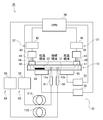
- FIG. 2 is a schematic diagram for explaining the reaction processing apparatus 30 according to the embodiment of the present invention.
- the reaction processing device 30 includes a reaction processing container mounting portion (not shown) on which the reaction processing container 10 is mounted, a temperature control system 32, and a CPU 36.
- the temperature control system 32 applies a temperature of about 95 ° C. to a region on the right side of the flow path 12 of the reaction processing container 10 with respect to the reaction processing container 10
- the high-temperature area) and the area on the left side of the drawing can be accurately maintained and controlled at about 60 ° C. (low-temperature area).
- the temperature control system 32 maintains the temperature of each temperature region of the reaction region.
- the temperature control system 32 includes a high-temperature heater 60 for heating the high-temperature region of the flow channel 12 and a low-temperature region of the flow channel 12.
- a temperature sensor (not shown) such as a thermocouple for measuring the actual temperature of each temperature region, and a high-temperature heater driver 33 for controlling the temperature of the high-temperature heater 60.
- a low-temperature heater driver 35 for controlling the temperature of the low-temperature heater 62.
- the actual temperature information measured by the temperature sensor is sent to the CPU 36.
- the CPU 36 controls each heater driver based on the actual temperature information of each temperature region so that the temperature of each heater becomes a predetermined temperature.
- Each heater may be, for example, a resistance heating element, a Peltier element, or the like.
- the temperature control system 32 may further include other component parts for improving the temperature controllability of each temperature region.
- the reaction processing apparatus 30 further includes a liquid sending system 37 for moving the sample 20 introduced into the flow channel 12 of the reaction processing container 10 within the flow channel 12.
- the liquid feeding system 37 includes a first pump 39, a second pump 40, a first pump driver 41 for driving the first pump 39, a second pump driver 42 for driving the second pump 40, A first tube 43 and a second tube 44 are provided.
- One end of the first tube 43 is connected to the first communication port 17 of the reaction processing container 10. It is preferable that a packing 45 and a seal for ensuring airtightness are arranged at a connection portion between the first communication port 17 and one end of the first tube 43. The other end of the first tube 43 is connected to the output of the first pump 39. Similarly, one end of a second tube 44 is connected to the second communication port 18 of the reaction processing container 10. It is preferable that a packing 46 and a seal for ensuring airtightness are arranged at a connection portion between the second communication port 18 and one end of the second tube 44. The other end of the second tube 44 is connected to the output of the second pump 40.
- the first pump 39 and the second pump 40 may be, for example, micro-blower pumps including a diaphragm pump.
- a micro blower pump model MZB1001T02 manufactured by Murata Manufacturing Co., Ltd. can be used. This micro-blower pump can increase the pressure on the secondary side from the primary side during operation, but the pressure on the primary side and the pressure on the secondary side become equal at the moment of stop or at the time of stop.
- the CPU 36 controls the blowing and pressurization from the first pump 39 and the second pump 40 via the first pump driver 41 and the second pump driver 42. Ventilation and pressurization from the first pump 39 and the second pump 40 act on the sample 20 in the flow path through the first communication port 17 and the second communication port 18 to move the sample 20 as a propulsive force. More specifically, by operating the first pump 39 and the second pump 40 alternately, the pressure applied to one of the end faces of the sample 20 becomes larger than the pressure applied to the other end, so that the propulsion related to the movement of the sample 20 is performed. Power is gained.
- the sample 20 can be reciprocated in the flow path and stopped at each temperature region of the flow path 12 of the reaction processing container 10, As a result, a thermal cycle can be given to the sample 20.
- the target DNA in the sample 20 is selectively amplified by repeatedly giving each step of denaturation in the high temperature region and annealing / extension in the low temperature region.
- the high temperature region can be regarded as the denaturation temperature region
- the low temperature region can be regarded as the annealing / elongation temperature region.
- the time during which the sample 20 stays in each temperature region can be appropriately set by changing the time during which the sample 20 stops at a predetermined position in each temperature region.
- the reaction processing device 30 further includes a first fluorescence detection device 50 and a second fluorescence detection device 54.
- the predetermined fluorescent dye is added to the sample 20. Since the intensity of the fluorescent signal emitted from the sample 20 increases as the amplification of the DNA proceeds, the intensity value of the fluorescent signal can be used as an index as a material for determining the progress of the PCR or the end of the reaction.
- the first fluorescence detection device 50 and the second fluorescence detection device 54 are Nippon Sheet Glass, which can measure quickly and detect fluorescence regardless of whether it is a bright place or a dark place with very compact optical system.
- An optical fiber type fluorescence detector FLE-510 manufactured by Co., Ltd. can be used.
- the wavelength characteristics of the excitation light / fluorescence can be tuned in advance so as to be suitable for the fluorescence characteristics emitted from the sample 20, and an optimal optical / detection system for samples having various characteristics is provided. It can be provided, and is suitable for detecting fluorescence from a sample present in a small or narrow area such as a flow path due to the small diameter of the light beam provided by the fiber optic fluorescence detector.
- the first fluorescence detection device 50 connects the first optical head 51, the first excitation light source / detector module 52 for fluorescence detection, and the first optical head 51 and the first excitation light source / detector module 52 for fluorescence detection. And an optical fiber F12.
- the second fluorescence detection device 54 includes a second optical head 55, a second excitation light source / detector module 56 for fluorescence detection, a second optical head 55, and a second excitation light source / detector module 56 for fluorescence detection.
- the first excitation light source / detector module 52 for detecting fluorescence and the second excitation light source / detector module 56 for detecting fluorescence respectively include a light source for excitation light, a wavelength multiplexer / demultiplexer, and a fluorescence detector for controlling these. Drivers etc. are included.
- the first optical head 51 and the second optical head 55 are each composed of an optical system such as a lens, and have a function of directional irradiation of the sample with the excitation light and a function of collecting fluorescence emitted from the sample.
- the fluorescent light collected by the first optical head 51 and the second optical head 55 passes through optical fibers F12 and F22, respectively, and the first excitation light source / detector module 52 for detecting fluorescence and the second excitation light source / detector module for detecting second fluorescence.
- the light is separated from the excitation light by the wavelength multiplexer / demultiplexer in 56 and is converted into an electric signal by the fluorescence detector. Details of the configuration of the fluorescence detection device will be described later.
- the fluorescence from the sample 20 passing through a part of the region 12a (referred to as the “first fluorescence detection region 12a”) in the connection region connecting the high temperature region and the low temperature region is obtained.
- the first optical head 51 is arranged so as to be able to detect.
- the second optical head 55 is arranged so as to be able to detect fluorescence from the sample 20 passing through another part of the connection region 12b (referred to as “second fluorescence detection region 12b”).
- the reaction proceeds, and the predetermined DNA contained in the sample 20 is amplified.
- the progress of the DNA amplification is monitored. Can be known in real time.
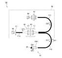
- FIG. 3 is a diagram for explaining the configuration of the fluorescence detection device.
- FIG. 3 illustrates the configuration of the first fluorescence detection device 50, but the second fluorescence detection device 54 has the same configuration except that the center wavelength of the bandpass filter is different.
- the first fluorescence detection device 50 includes a first optical head 51, a first excitation light source for fluorescence detection / detector module 52, a first optical head 51, and a first excitation light source for fluorescence detection / An optical fiber F12 for connecting to the detector module 52.
- the first fluorescence detection excitation light source / detector module 52 includes a first excitation light source 64, a first wavelength multiplexer / demultiplexer 65, and a first fluorescence detector 66, and these functional elements are optical fibers. The excitation light and the fluorescent light propagate in the optical fiber.
- a bandpass filter A1 is arranged near the first excitation light source 64 so that the excitation light emitted from the first excitation light source 64 is transmitted.
- the first wavelength multiplexer / demultiplexer 65 has a bandpass filter B1.
- a band-pass filter C1 is arranged near the first fluorescence detector 66 so that the fluorescence incident on the first fluorescence detector 66 is transmitted.
- the wavelength characteristics of these bandpass filters are designed according to the wavelength characteristics related to excitation / fluorescence of a fluorescent dye such as FAM.
- Each bandpass filter transmits light in a specific wavelength range with high efficiency (for example, transmittance of 75% or more) and reflects light of other wavelengths with high efficiency (for example, reflectance of 75% or more; (Preferably 85% or more).
- the first fluorescence detection device 50 is configured to be able to detect fluorescence from a sample containing FAM as a fluorescent dye.
- the first excitation light source 64 is not particularly limited as long as it is a light source capable of separating light having a desired wavelength later.
- a light source capable of separating light having a desired wavelength later.
- an LD, an LED, a white light source or the like can be used.
- Excitation light emitted from the first excitation light source 64 is separated by the band-pass filter A1, and only light within a predetermined range having a center wavelength of about 470 nm (hereinafter referred to as “excitation light OE1”) is transmitted through the optical fiber F11. Is propagated.
- the pumping light OE1 enters the first wavelength multiplexer / demultiplexer 65, and reaches the bandpass filter B1 after being collimated by the lens L1. Since the bandpass filter B1 is designed to reflect the excitation light OE1, the excitation light OE1 is condensed again by the lens L1 and enters the optical fiber F12. The pumping light OE1 propagates through the optical fiber F12 and reaches the first optical head 51.
- the first optical head 51 is provided with a first objective lens OB1, and the excitation light OE1 irradiates the sample 20 as excitation light at a predetermined working distance.
- FIG. 3 shows an example in which a gradient index lens is used as the first objective lens OB1.
- the fluorescent dye in the sample 20 is excited, and the sample 20 emits the fluorescent OF1.
- the fluorescent light OF1 is collected by the first objective lens OB1 of the first optical head 51, enters the optical fiber F12, and propagates in the optical fiber F12.
- the fluorescent light OF1 enters the first wavelength multiplexer / demultiplexer 65, and reaches the bandpass filter B1 after being collimated by the lens L1.
- the wavelength of the fluorescent light generated by the irradiation of the excitation light is longer than the wavelength of the excitation light. That is, when the center wavelength of the excitation light is ⁇ e and the center wavelength of the fluorescence is ⁇ f, ⁇ e ⁇ f. Therefore, in order to guide only the fluorescence OF1 to the first fluorescence detector 66, a bandpass filter B1 having a spectral characteristic of reflecting light of the wavelength ⁇ e and transmitting light of the wavelength ⁇ f is used as the bandpass filter B1.
- the bandpass filter B1 is designed to transmit light of a wavelength that does not overlap with the wavelength of the excitation light OE1 of the fluorescence OF1.
- the fluorescence OF1 that has passed through the band-pass filter B1 is condensed by the lens L2 and enters the optical fiber F13. Further, since the band-pass filter B1 has a function of reflecting the excitation light and transmitting the fluorescence, it reflects light in the wavelength range including ⁇ e and transmits light in the wavelength range including ⁇ f, corresponding to the center wavelength. Edge filters that can be used can be used instead of bandpass filters.
- the fluorescence OF1 that has propagated in the optical fiber F13 reaches the first fluorescence detector 66.
- the fluorescence OF1 may pass through the band-pass filter C1 before entering the first fluorescence detector 66 in order to strictly adjust the wavelength range. Only light having a center wavelength of about 530 nm and having a wavelength within a predetermined range, which has passed through the band-pass filters B1 and C1, is incident on the first fluorescence detector 66.
- the first fluorescence detector 66 is a photoelectric conversion element such as a PD, an APD, and a photomultiplier (photomultiplier). The signal converted into an electric signal by the first fluorescence detector 66 is subjected to signal processing described later.
- each element may include a lens for efficiently transmitting and coupling light or improving the use efficiency of a bandpass filter.
- a lens for efficiently transmitting and coupling light or improving the use efficiency of a bandpass filter.
- a gradient index lens, a ball lens, an aspheric lens, or the like can be used.
- a single mode fiber or a multi mode fiber can be used as the optical fibers F11, F12 and F13.
- the first fluorescence detection device 50 configured as described above irradiates the sample with light having a center wavelength of 470 nm and a wavelength range of about 450 to 490 nm as the first excitation light OE1, and emits the center wavelength emitted from the sample. Is 530 nm and the first fluorescence OF1 having a wavelength range of about 510 to 550 nm is detected. Those skilled in the art can understand that the characteristics related to the wavelength are determined by the combination of the transmission or reflection characteristics of each band-pass filter as described above, and these can be changed or customized.
- the second fluorescence detection device 54 is configured to be able to detect fluorescence from a sample containing ROX as a fluorescent dye.
- the second fluorescence detector 54 irradiates the sample with light having a center wavelength of 530 nm and a wavelength range of about 510 to 550 nm as the second excitation light OE2, and has a center wavelength of 610 nm and a wavelength range of about 580 to 640 nm.
- the second fluorescent OF2 is detected.
- FIG. 4 shows a state where the first optical head 51 of the first fluorescence detection device 50 and the second optical head 55 of the second fluorescence detection device 54 are arranged.
- the first optical head 51 is arranged so as to detect fluorescence from the sample 20 passing through the first fluorescence detection area 12a of the flow channel 12.
- the second optical head 55 is arranged so that fluorescence can be detected from the sample 20 passing through the second fluorescence detection region 12b of the flow channel 12.
- the first optical head 51 and the second optical head 55 are held by a holding member (not shown in FIG. 4, but see FIG. 5).
- the first optical head 51 condenses the first excitation light OE1 propagated in the optical fiber F12 by the first objective lens OB1, and irradiates the sample 20 passing through the first fluorescence detection area 12a. Then, the first fluorescent light OF1 generated from the sample 20 is condensed by the first objective lens OB1, and is incident on the optical fiber F12.
- the second optical head 55 condenses the second excitation light OE2 propagated in the optical fiber F22 with the second objective lens OB2, irradiates the second excitation light OE2 onto the sample 20 passing through the second fluorescence detection region 12b, and Is collected by the second objective lens OB2 and is incident on the optical fiber F22.
- first objective lens OB1 and the second objective lens OB2 a lens or a lens group having a positive power, for example, a SELFOC (registered trademark) microlens that is a refractive index distribution lens can be used.
- SELFOC registered trademark
- first objective lens OB1 and the second objective lens OB2 for example, those having a diameter of 1.8 mm, a numerical aperture (NA) of 0.23, and a working distance (WD) of 1 mm to 3 mm can be used.
- the first excitation light source of the first fluorescence detection device 50 is modulated by the first modulation signal and emits light in a blinking manner.
- the second excitation light source of the second fluorescence detection device 54 is modulated by the second modulation signal and emits light in a blinking manner.
- the first optical head 51 and the second optical head 55 are arranged side by side in the longitudinal direction of the flow channel 12 in order to detect the sample 20 passing through one flow channel 12.
- the first fluorescence detection device 50 irradiates the first excitation light OE1 having a center wavelength of 470 nm and a wavelength range of about 450 to 490 nm, and has a center wavelength of 530 nm and a wavelength range of about 510 to 550 nm. A certain first fluorescence OF1 is detected.
- the second fluorescence detector 54 irradiates the second excitation light OE2 having a center wavelength of 530 nm and a wavelength range of about 510 to 550 nm, and a second excitation light OE2 having a center wavelength of 610 nm and a wavelength range of about 580 to 640 nm.
- the fluorescent OF2 is detected. Therefore, the wavelength range of the second excitation light OE2 (about 510 to 550 nm) and the wavelength range of the first fluorescence OF1 (about 510 to 550 nm) overlap.
- the second excitation light OE2 when a part of the second excitation light OE2 emitted from the second optical head 55 is detected by the first optical head 51, the second excitation light OE2 is supplied to a band-pass filter at the subsequent stage of the first optical head 51. There is a possibility that the light is not removed by B1 and C1 and reaches the first fluorescence detector 66.
- the second excitation light OE2 is noise in the first fluorescence detector 66, and there is a possibility that the first fluorescence OF1, which should be detected, cannot be detected.
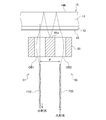
- FIG. 5 is a diagram showing a model of the optical simulation.
- the first objective lens OB1 and the second objective lens OB2 have a diameter of 1.8 mm, a central refractive index of 1.616 (@ 530 nm), ⁇ A (optical constant) of 0.346 mm ⁇ 1 (@ 530 nm), A gradient index lens having a lens length of 4.45 mm was used.
- the optical fibers F12 and F22 were multimode fibers having a core diameter of 200 ⁇ m, a cladding diameter of 220 ⁇ m, and an NA of 0.3.
- the working distance between the objective lens and the multimode fiber was 1.8 mm.
- the first objective lens OB1 and the second objective lens OB2 are held by a holding member 61 made of stainless steel.
- the distance between the optical axis of the first objective lens OB1 and the optical axis of the second objective lens OB2 is referred to as “center-to-center distance P”.
- Side surfaces of the first objective lens OB1 and the second objective lens OB2 are fixed to the holding member 61 via an epoxy adhesive layer having a thickness of 10 ⁇ m.
- the upper surface 61a of the holding member 61 is flush with the end faces on the excitation light emission side of the first objective lens OB1 and the second objective lens OB2.
- a 4 mm-thick cycloolefin polymer substrate (refractive index 1.53) was used as the substrate 14.
- a channel 12 having a square cross section with a width of 0.7 mm and a depth of 0.7 mm is formed, and the lower surface of the channel 12 is sealed with a channel sealing film 16 (cycloolefin) having a thickness of 0.1 mm. It was made of polymer and sealed with a refractive index of 1.53).
- the distance between the objective lens and the sample is based on a working distance of 1.8 mm (matched with the working distance between the objective lens and the multi-mode fiber), which is the same magnification imaging system, and the flow path is sealed in the optical path.
- the light beam (corresponding to the excitation light) emitted from the second objective lens OB2 of the second optical head 55 is transmitted through the flow path 12, reflected by the second main surface 14b of the substrate 14, and The reflected light passes through the flow path 12 in the opposite direction. Thereafter, the light beam is reflected on the upper surface 61a of the holding member 61 between the two objective lenses, passes through the flow path 12 again, and is reflected on the second main surface 14b of the substrate 14. The reflected light again passes through the flow path 12 in the reverse direction, is received by the first objective lens OB1 of the first optical head 51, and is emitted through the optical fiber F12. From this optical simulation, it was found that the excitation light emitted from one optical head circulated as noise to the other optical head due to such an optical path.
- FIG. 6 is a diagram illustrating the derivation of the center distance P between two optical heads.
- the light beam emitted from the second objective lens OB2 of the second optical head 55 and received by the first objective lens OB1 of the first optical head 51 Is the angle between the optical axis of the second objective lens OB2 (the incident angle with respect to the flow path sealing film 16) and ⁇ , the air layer 63 between the second objective lens OB2 and the flow path sealing film 16 and the flow path sealing film.
- the angle of refraction at the interface with the channel 16 is ⁇ 1
- the angle of refraction at the interface between the channel sealing film 16 and the channel 12 is ⁇ 2
- the angle of refraction at the interface between the channel 12 and the substrate 14 is ⁇ 3
- the refractive index of the flow path sealing film 16 is n 1
- the refractive index of the flow path 12 is n 2 (differs depending on whether a sample exists in the flow path 12 or not (ie, in the case of air))
- the refractive index and n 3 the Snell's law for each interface
- the center-to-center distance P between the two optical heads can be expressed as the following equation (2) as the sum of the longitudinal components of the optical path in the flow path.
- P (L ⁇ tan ⁇ + t 1 ⁇ tan ⁇ 1 + 2 ⁇ t 2 ⁇ tan ⁇ 2 + 2 ⁇ t 3 ⁇ tan ⁇ 3 )
- ⁇ 2 2 ⁇ L ⁇ tan ⁇ + 2 ⁇ t 1 ⁇ tan ⁇ 1 + 4 ⁇ t 2 ⁇ tan ⁇ 2 + 4 ⁇ t 3 ⁇ tan ⁇ 3 (2)
- L is the distance from the upper surface 61a of the holding member 61 to the flow path seal film 16 (mm)
- the thickness of t 1 is the flow path seal film 16 (mm)
- t 2 is the channel 12 depth (mm)
- t 3 is the thickness from the bottom of the channel 12 to the second main surface 14b of the substrate 14 (mm).
- Equation (1) 2 ⁇ L ⁇ sin ⁇ / ⁇ (1 ⁇ sin 2 ⁇ ) + 2 ⁇ t 1 ⁇ sin ⁇ 1 / ⁇ (1 ⁇ sin 2 ⁇ 1 ) + 4 ⁇ t 2 ⁇ sin ⁇ 2 / ⁇ (1 ⁇ sin 2 ⁇ 2 ) + 4 ⁇ t 3 ⁇ sin ⁇ 3 / ⁇ (1 ⁇ sin 2 ⁇ 3 ) (5)
- the third term on the right side becomes large when n 2 is small (that is, when the sample is not contained in the flow channel 12 and the air is air), and the center-to-center distance P becomes ⁇ at the maximum value ⁇ .
- the maximum value P max is obtained.
- P max 2 ⁇ P 0 + 2 ⁇ P 1 + 4 ⁇ P 2 + 4 ⁇ P 3 (7)
- P 0 L ⁇ NA / ⁇ (1 ⁇ NA 2 )
- P 1 t 1 ⁇ NA / ⁇ (n 1 2 -NA 2)
- P 2 t 2 ⁇ NA / ⁇ (1-NA 2 )
- P 3 t 3 ⁇ NA / ⁇ (n 3 2 -NA 2 )
- the center distance P satisfies the following expression (8).
- P max 2 ⁇ P 0 + 2 ⁇ P 1 + 4 ⁇ P 2 + 4 ⁇ P 3 ⁇ P (8)
- 1.1 ⁇ P max ⁇ P that is, safety factor 1.1
- 1.2 ⁇ P max ⁇ P that is, safety factor 1.2
- the upper limit of the center-to-center distance P can be determined according to the length S (mm) of the linear portion of the flow path 12 where the two optical heads are arranged.
- the length S of the straight portion of the flow channel 12 is the length of the connection region in the flow channel 12 (see FIG. 1).
- each of the first optical head 51 and the second optical head 55 is disposed such that the optical axis is located inside by a predetermined length ⁇ S (mm) from the end of the linear portion of the flow channel 12. That is, the two optical heads are preferably arranged so that the center-to-center distance P satisfies P ⁇ S ⁇ 2 ⁇ ⁇ S.
- ⁇ S may be 1 mm.
- the flow path 12 has a square cross section.
- the cross section of the flow path 12 may be, for example, a rectangle, a trapezoid, a semicircle, or any other shape.
- a point intersecting with the optical axis of the channel 12 can be treated as the bottom of the flow channel 12 in the same manner as described above.
- a light absorbing layer that absorbs excitation light may be provided between the bottom of the flow channel 12 in the substrate 14 and the second main surface 14b.
- excitation light circulating from one optical head (second optical head 55) to the other optical head (first optical head 51) as noise light is applied to the bottom of the flow channel 12 in the substrate 14 and the second optical head.
- the light passes through the gap with the main surface 14b four times. Therefore, by providing the light absorbing layer between the bottom of the flow path 12 in the substrate 14 and the second main surface 14b, noise light circulating from one optical head to the other optical head can be attenuated. It is possible to reliably suppress interference between the fluorescence detection devices.
- Example 1 In the first embodiment, in the configuration shown in FIG. 5, the upper surface 61a of the holding member 61 between the two objective lenses is mirror-finished (light reaching the upper surface 61a is reflected according to Snell's law in order to emphasize and evaluate the reflected light.
- FIG. 7 shows a change in the relative intensity of the light beam when the distance P between the centers of the two optical heads is changed in the range of 2.5 mm to 8.0 mm.
- a gradient index lens having a specification capable of effectively capturing light emitted from a multi-mode fiber with an NA of 0.3 is used as an objective lens.
- the configuration is such that the working distances on the emission side are equal (equal-magnification imaging system). Therefore, the NA corresponding to the opening angle, which is the angle at which the incident light is viewed from the focal position on the optical axis in the absence of the flow path sealing film 16, may be considered to be substantially equal to the NA of the light emitted from the multimode fiber. it can.
- Example 2 In Example 2, a pinhole of ⁇ 0.8 mm was arranged on the emission end face of the second objective lens OB2 of the second optical head 55. Other conditions were the same as in Example 1, and the intensity of the light beam reaching the evaluation surface was determined by optical simulation.
- FIG. 8 shows a change in the relative intensity of the light beam when the distance P between the centers of the two optical heads is changed in the range of 2.5 mm to 6.0 mm.
- L 1.735 mm
- NA 0.22
- t 1 0.1 mm
- t 2 0.7 mm
- t 3 3.3 mm
- the absorbance of a substance can be represented by ⁇ ln (I / I 0 ).
- the absorbance of the light absorbing layer may be set to --1 ⁇ ln (0.1) ⁇ 0.58. Therefore, if the absorbance A of the light absorbing layer of the substrate 14 satisfies A ⁇ 0.58, the intensity of the noise light circulating from one optical head to the other optical head can be reduced to 10% or less.
- the actual rays, as shown in FIG 6, is incident at an angle theta 3 to light-absorbing layer of the substrate 14.
- the thickness of the light absorbing layer is t 3 ′
- the optical path length when transmitted once through the light absorbing layer is t 3 ′ / cos ⁇ 3 , but with a margin
- the minimum value t 3 ′ is treated as the optical path length.
- the light absorbing layer may be provided so as to satisfy the absorption coefficient ⁇ ⁇ 0.58 / t 3 ′ at the thickness t 3 ′.
- the light absorbing layer that reduces the noise light to 10% has been described. However, it is more preferable that the noise light can be reduced to 5%, and it is more preferable that the noise light can be reduced to 1%.
- the light is adjusted so as to satisfy the absorption coefficient ⁇ ⁇ ⁇ / ⁇ ln (0.05) / t 3 ⁇ ⁇ 0.75 / t 3 ′ ”for the target wavelength. What is necessary is just to provide an absorption layer.
- the absorption coefficient ⁇ ⁇ ⁇ / ⁇ ln (0.01) / t 3 ′ ⁇ 1.15 / t 3 ′ should be satisfied for the target wavelength. May be provided with a light absorbing layer.
- the light-absorbing layer may be provided on the entire surface of the substrate 14 between the bottom of the flow path 12 and the second main surface 14b by forming the substrate 14 itself from a light-absorbing material. May be provided in a part of the vertical direction.
- a light absorbing layer may be separately provided on the second main surface 14b of the substrate 14 in a state where the refractive index is matched with that of the substrate 14.
- “a state in which the refractive index is matched” means that the difference in the refractive index before and after the interface is 0.025 or less.
- the third embodiment is an embodiment in which a light absorbing layer is provided on the whole of the substrate 14 between the bottom of the flow channel 12 and the second main surface 14b.
- L 1.735 mm
- NA 0.3
- t 1 0.1 mm
- t 2 0.7 mm
- t 3 3.3 mm
- n 1 1. 53
- n 3 1.53.
- the intensity of a light beam reaching the evaluation surface was determined by optical simulation in the same manner as in Example 1.
- Example 3 As a result of the optical simulation, in Example 3, the relative noise amount was 0.02 when no sample was present in the flow channel 12 and was 0.03 when the sample was present in the flow channel 12.
- the relative noise amount when the sample does not exist in the flow channel 12 is 0.19. Since the relative noise amount when present was 0.31, it was confirmed that the third embodiment in which the light absorbing layer was provided on the substrate 14 could reduce the noise amount to about 10% as compared with the first embodiment.
- Embodiment 4 is an embodiment in which a light absorbing layer is provided on the second main surface 14b of the substrate 14.
- a 0.8 mm pinhole is arranged on the emission end face of the second objective lens OB2 of the second optical head 55.
- a refractive index of 1.53 and a thickness of 0.1 mm are provided on the second main surface 14b of the substrate 14 via a substantially non-absorbing resin layer having a refractive index of 1.53 and a thickness of 0.1 mm.
- Example 4 As a result of the optical simulation, in Example 4, the relative noise amount was 0.1. From FIG. 8, in the second embodiment, when the distance P between the center points is 2.75 mm, the relative noise amount when the sample exists in the flow channel 12 is 0.85. It was confirmed that Example 4 in which the light absorbing layer was provided on the surface 14b could reduce the noise amount to about 12% as compared with Example 2.
- Example 5 In the fifth embodiment, only the absorption coefficient of the light absorption layer provided on the second main surface 14b of the substrate 14 is changed from the fourth embodiment.
- Example 5 in which the absorption coefficient ⁇ of the light absorbing layer was 7.5 cm ⁇ 1 , the refractive index of the resin layer provided between the substrate 14 and the light absorbing layer was 1.530 to 1.505 (refractive index). (Difference: 0.025), and the same optical simulation was performed. The maximum intensity of the light beam reaching the evaluation surface was 2% as compared with the case where the refractive index of the resin layer was 1.530. It was only increasing.
- Example 6 Also in Example 6, only the absorption coefficient of the light absorption layer provided on the second main surface 14b of the substrate 14 was changed from Example 4.
- the intensity of the light beam that reaches the evaluation surface is obtained by optical simulation as in the above-described embodiment.
- the present invention can be used for the polymerase chain reaction (PCR).
- PCR polymerase chain reaction
Abstract
Description
sinθ=n1・sinθ1=n2・sinθ2=n3・sinθ3 ・・・(1)
P=(L・tanθ+t1・tanθ1+2・t2・tanθ2+2・t3・tanθ3)×2
=2・L・tanθ+2・t1・tanθ1+4・t2・tanθ2+4・t3・tanθ3 ・・・(2)
(2)式において、Lは保持部材61の上面61aから流路封止フィルム16までの距離(mm)、t1は流路封止フィルム16の厚さ(mm)、t2は流路12の深さ(mm)、t3は流路12の底部から基板14の第2主面14bまでの厚さ(mm)である。
1/tan2θ+1=1/sin2θ ・・・(3)
(3)式を変形すると、以下の(4)式が得られる。
tanθ=sinθ/√(1-sin2θ) ・・・(4)
P=2・L・sinθ/√(1-sin2θ)+2・t1・sinθ1/√(1-sin2θ1)+4・t2・sinθ2/√(1-sin2θ2)+4・t3・sinθ3/√(1-sin2θ3) ・・・(5)
(5)式に(1)式を代入すると、以下の(6)式が得られる。
P=2・L・sinθ/√(1-sin2θ)+2・t1・sinθ/(√(n1 2-sin2θ))+4・t2・sinθ/√(n2 2-sin2θ)+4・t3・sinθ/√(n3 2-sin2θ) ・・・(6)
Pmax=2・P0+2・P1+4・P2+4・P3 ・・・(7)
ただし、P0=L・NA/√(1-NA2)
P1=t1・NA/√(n1 2-NA2)
P2=t2・NA/√(1-NA2)
P3=t3・NA/√(n3 2-NA2)
Pmax=2・P0+2・P1+4・P2+4・P3<P ・・・(8)
中心間距離Pが(8)式を満たすように光学ヘッドを配置することにより、一方の光学ヘッドから照射された励起光の他方の光学ヘッドへの回り込みを回避できるので、蛍光検出装置間の干渉を抑制できる。その結果、安定した蛍光信号が得られ、良好な測定精度を有する反応処理装置を実現することができる。
(実施例1)
実施例1では、図5に示す構成において、反射光を強調して評価するために2つの対物レンズ間の保持部材61の上面61aを鏡面(上面61aに到達した光がスネルの法則に従って反射する面)とし、第2光学ヘッド55の光ファイバF22の端面の近傍から、φ200μm(マルチモードファイバのコア径に対応)且つランバシャン17.5°(マルチモードファイバのNA(0.3)に対応)の条件で、光ファイバF22に向けて25000本の光線(波長530nm)を出射させ、第1光学ヘッド51の光ファイバF12の端面の近傍に配置した評価面に到達する光線の強度を光学シミュレーションにより求めた。2つの光学ヘッドの中心間距離Pを2.5mm~8.0mmの範囲で変えたときの光線の相対強度の変化を図7に示す。
実施例2では、第2光学ヘッド55の第2対物レンズOB2の出射端面にφ0.8mmのピンホールを配置した。それ以外の条件は実施例1と同様とし、評価面に到達する光線の強度を光学シミュレーションにより求めた。2つの光学ヘッドの中心間距離Pを2.5mm~6.0mmの範囲で変えたときの光線の相対強度の変化を図8に示す。
(実施例3)
実施例3は、基板14における流路12の底部と第2主面14bとの間の全体に光吸収層を設けた実施例である。実施例3では、実施例1と同様に、L=1.735mm、NA=0.3、t1=0.1mm、t2=0.7mm、t3=3.3mm、n1=1.53、n3=1.53とした。実施例3では、中心点間距離Pを3.5mmとし、実施例1で求めたPmax=4.65mmよりも小さい値とした。基板14における流路12の底部と第2主面14bとの間に、厚みt3’=3.3mmで吸収係数α=0.58/0.33=1.76cm-1の光吸収層を設け、実施例1と同様に評価面に到達する光線の強度を光学シミュレーションにより求めた。
実施例4は、基板14の第2主面14b上に光吸収層を設けた実施例である。実施例4では、実施例2と同様に、第2光学ヘッド55の第2対物レンズOB2の出射端面にφ0.8mmのピンホールを配置した構成とした。実施例4では、中心点間距離Pを2.75mmとし、実施例2で求めたPmax=3.36mmよりも小さい値とした。また、実施例4では、基板14の第2主面14b上に、屈折率1.53で厚さ0.1mmの実質的に吸収のない樹脂層を介して、屈折率1.53、厚さ1.0mmで吸収係数α=0.58/0.1=5.8cm-1の光吸収層を設け、流路12内に試料が存在する条件で上記実施例と同様に評価面に到達する光線の強度を光学シミュレーションで求めた。
実施例5では、基板14の第2主面14b上に設ける光吸収層の吸収係数のみ実施例4から変更した。実施例5では、光吸収層の吸収係数αを、α=0.75/0.1=7.5cm-1とし、上記実施例と同様に評価面に到達する光線の強度を光学シミュレーションで求めた。
実施例6においても、基板14の第2主面14b上に設ける光吸収層の吸収係数のみ実施例4から変更した。実施例6では、光吸収層の吸収係数αを、α=1.15/0.1=11.5cm-1とし、上記実施例と同様に評価面に到達する光線の強度を光学シミュレーションで求めた。
Claims (10)
- 試料が移動する流路が第1主面に形成された基板と、前記流路を封止するように前記第1主面上に設けられた流路封止フィルムとを備える反応処理容器と、
第1励起光を前記流路中の試料に照射するとともに、前記第1励起光の照射により試料から生じた第1蛍光を集光する第1対物レンズを備える第1光学ヘッドと、
第2励起光を前記流路中の試料に照射するとともに、前記第2励起光の照射により試料から生じた第2蛍光を集光する第2対物レンズを備える第2光学ヘッドと、
前記第1光学ヘッドおよび前記第2光学ヘッドを保持する保持部材と、
を備える反応処理装置であって、
前記第1光学ヘッドおよび前記第2光学ヘッドは、前記流路の長手方向に並んで配置され、
前記第1蛍光の波長範囲と前記第2励起光の波長範囲は、少なくとも一部が重複しており、
前記第1対物レンズの光軸と前記第2対物レンズの光軸との間の距離Pが、以下の式:
2・P0+2・P1+4・P2+4・P3<P
P0=L・NA/√(1-NA2)
P1=t1・NA/√(n1 2-NA2)
P2=t2・NA/√(1-NA2)
P3=t3・NA/√(n3 2-NA2)
を満たす(ただし、Lは前記保持部材から前記流路封止フィルムまでの距離、t1は前記流路封止フィルムの厚さ、t2は前記流路の深さ、t3は前記流路の底部から前記基板の第2主面までの厚さ、NAは前記第1対物レンズおよび前記第2対物レンズの開口数、n1は前記流路封止フィルムの屈折率、n3は前記基板の屈折率)ことを特徴とする反応処理装置。 - 前記距離Pが、さらに1.1×(2・P0+2・P1+4・P2+4・P3)≦Pを満たし、さらに好ましくは1.2×(2・P0+2・P1+4・P2+4・P3)≦Pを満たすことを特徴とする請求項1に記載の反応処理装置。
- 前記距離Pが、P≦S-2×ΔS(ただし、Sは前記第1光学ヘッドおよび前記第2光学ヘッドが配置される流路の直線部分の長さ、ΔSは1mm)を満たすことを特徴とする請求項1または2に記載の反応処理装置。
- 前記基板における前記流路の底部と前記第2主面との間に、励起光を吸収する光吸収層を備えることを特徴とする請求項1から3のいずれかに記載の反応処理装置。
- 試料が移動する流路が第1主面に形成された基板と、前記流路を封止するように前記第1主面上に設けられた流路封止フィルムとを備える反応処理容器と、
第1励起光を前記流路中の試料に照射するとともに、前記第1励起光の照射により試料から生じた第1蛍光を集光する第1対物レンズを備える第1光学ヘッドと、
第2励起光を前記流路中の試料に照射するとともに、前記第2励起光の照射により試料から生じた第2蛍光を集光する第2対物レンズを備える第2光学ヘッドと、
前記第1光学ヘッドおよび前記第2光学ヘッドを保持する保持部材と、
を備える反応処理装置であって、
前記第1光学ヘッドおよび前記第2光学ヘッドは、前記流路の長手方向に並んで配置され、
前記第1蛍光の波長範囲と前記第2励起光の波長範囲は、少なくとも一部が重複しており、
前記基板に励起光を吸収する光吸収層が設けられることを特徴とする反応処理装置。 - 前記光吸収層は、吸収係数αがα≧0.58/t3’(ただしt3’は前記光吸収層の厚さ)を満たすように形成されることを特徴とする請求項5に記載の反応処理装置。
- 前記光吸収層は、吸収係数αがα≧0.75/t3’(ただしt3’は前記光吸収層の厚さ)を満たすように形成されることを特徴とする請求項5に記載の反応処理装置。
- 前記光吸収層は、吸収係数αがα≧1.15/t3’(ただしt3’は前記光吸収層の厚さ)を満たすように形成されることを特徴とする請求項5に記載の反応処理装置。
- 前記光吸収層は、前記流路の底部と前記基板の第2主面との間に設けられることを特徴とする請求項5から8のいずれかに記載の反応処理装置。
- 前記光吸収層は、前記基板の第2主面上に設けられることを特徴とする請求項5から8のいずれかに記載の反応処理装置。
Priority Applications (6)
| Application Number | Priority Date | Filing Date | Title |
|---|---|---|---|
| BR112020025833-4A BR112020025833A2 (pt) | 2018-07-06 | 2019-06-26 | dispositivo de tratamento de reação |
| CN201980044608.5A CN112400106A (zh) | 2018-07-06 | 2019-06-26 | 反应处理装置 |
| SG11202012468SA SG11202012468SA (en) | 2018-07-06 | 2019-06-26 | Reaction treatment device |
| EP19829747.5A EP3819630A4 (en) | 2018-07-06 | 2019-06-26 | REACTION TREATMENT DEVICE |
| US17/124,655 US20210102897A1 (en) | 2018-07-06 | 2020-12-17 | Reaction processor |
| IL279951A IL279951A (en) | 2018-07-06 | 2021-01-04 | A device for treating a reaction |
Applications Claiming Priority (2)
| Application Number | Priority Date | Filing Date | Title |
|---|---|---|---|
| JP2018-129123 | 2018-07-06 | ||
| JP2018129123A JP6688342B2 (ja) | 2018-07-06 | 2018-07-06 | 反応処理装置 |
Related Child Applications (1)
| Application Number | Title | Priority Date | Filing Date |
|---|---|---|---|
| US17/124,655 Continuation US20210102897A1 (en) | 2018-07-06 | 2020-12-17 | Reaction processor |
Publications (1)
| Publication Number | Publication Date |
|---|---|
| WO2020008972A1 true WO2020008972A1 (ja) | 2020-01-09 |
Family
ID=69059616
Family Applications (1)
| Application Number | Title | Priority Date | Filing Date |
|---|---|---|---|
| PCT/JP2019/025331 WO2020008972A1 (ja) | 2018-07-06 | 2019-06-26 | 反応処理装置 |
Country Status (8)
| Country | Link |
|---|---|
| US (1) | US20210102897A1 (ja) |
| EP (1) | EP3819630A4 (ja) |
| JP (1) | JP6688342B2 (ja) |
| CN (1) | CN112400106A (ja) |
| BR (1) | BR112020025833A2 (ja) |
| IL (1) | IL279951A (ja) |
| SG (1) | SG11202012468SA (ja) |
| WO (1) | WO2020008972A1 (ja) |
Citations (11)
| Publication number | Priority date | Publication date | Assignee | Title |
|---|---|---|---|---|
| JP2005091242A (ja) * | 2003-09-19 | 2005-04-07 | Hitachi High-Technologies Corp | 電気泳動分析装置 |
| JP2007071608A (ja) * | 2005-09-05 | 2007-03-22 | Sharp Corp | 電気泳動装置および装置構成器具 |
| JP2007285999A (ja) * | 2006-04-20 | 2007-11-01 | Furukawa Electric Co Ltd:The | 光測定装置 |
| JP2008157814A (ja) * | 2006-12-25 | 2008-07-10 | Sharp Corp | 分析用基板および分析装置 |
| JP2009232700A (ja) | 2008-03-26 | 2009-10-15 | Shimadzu Corp | 反応処理方法及び反応処理装置 |
| JP2011027748A (ja) * | 2001-08-28 | 2011-02-10 | Baylor College Of Medicine | カラーブラインド蛍光のためのパルスマルチライン励起法 |
| JP2013524169A (ja) * | 2010-03-25 | 2013-06-17 | クァンタライフ・インコーポレーテッド | 液滴によるアッセイ用の検出システム |
| JP2015514218A (ja) * | 2012-04-03 | 2015-05-18 | イラミーナ インコーポレーテッド | 核酸シークエンシングに有用な統合化した読取りヘッド及び流体カートリッジ |
| JP2016095315A (ja) * | 2009-01-08 | 2016-05-26 | アイティ−アイエス インターナショナル リミテッドIt−Is International Ltd | 化学および/または生化学反応のための光学システム |
| WO2016157270A1 (ja) * | 2015-03-31 | 2016-10-06 | 日本電気株式会社 | 分光解析装置、分光解析方法、及び可読媒体 |
| WO2017145230A1 (ja) * | 2016-02-22 | 2017-08-31 | 株式会社日立ハイテクノロジーズ | 発光検出装置 |
Family Cites Families (9)
| Publication number | Priority date | Publication date | Assignee | Title |
|---|---|---|---|---|
| US7629124B2 (en) * | 2006-06-30 | 2009-12-08 | Canon U.S. Life Sciences, Inc. | Real-time PCR in micro-channels |
| KR101334183B1 (ko) * | 2007-06-01 | 2013-12-02 | 삼성전자주식회사 | 미세 반응을 위한 형광 검출 모듈과 이를 구비한 형광 검출시스템 |
| JP2009036538A (ja) * | 2007-07-31 | 2009-02-19 | Nippon Sheet Glass Co Ltd | 蛍光検出用のプローブ及び蛍光検出システム |
| JP5279481B2 (ja) * | 2008-12-25 | 2013-09-04 | 株式会社日立ハイテクノロジーズ | 核酸分析装置 |
| JP5297887B2 (ja) * | 2009-05-19 | 2013-09-25 | 日本板硝子株式会社 | 蛍光分析用光分波検出器及び蛍光検出システム |
| CN202057580U (zh) * | 2011-04-23 | 2011-11-30 | 浙江大学 | 用于定量pcr仪荧光检测的光学系统 |
| KR101969076B1 (ko) * | 2012-02-01 | 2019-08-13 | 주식회사 미코바이오메드 | 광 노이즈 제거 수단이 구현된 실시간 pcr 칩 및 이를 포함하는 pcr 장치 |
| WO2017115863A1 (ja) * | 2015-12-28 | 2017-07-06 | 凸版印刷株式会社 | マイクロ流体デバイスおよび観察方法 |
| SG10201911933TA (en) * | 2016-01-05 | 2020-02-27 | Nippon Sheet Glass Company Limited | Reaction treatment device, reaction treatment container, and reaction treatment method |
-
2018
- 2018-07-06 JP JP2018129123A patent/JP6688342B2/ja active Active
-
2019
- 2019-06-26 CN CN201980044608.5A patent/CN112400106A/zh active Pending
- 2019-06-26 EP EP19829747.5A patent/EP3819630A4/en active Pending
- 2019-06-26 BR BR112020025833-4A patent/BR112020025833A2/pt not_active IP Right Cessation
- 2019-06-26 SG SG11202012468SA patent/SG11202012468SA/en unknown
- 2019-06-26 WO PCT/JP2019/025331 patent/WO2020008972A1/ja unknown
-
2020
- 2020-12-17 US US17/124,655 patent/US20210102897A1/en active Pending
-
2021
- 2021-01-04 IL IL279951A patent/IL279951A/en unknown
Patent Citations (11)
| Publication number | Priority date | Publication date | Assignee | Title |
|---|---|---|---|---|
| JP2011027748A (ja) * | 2001-08-28 | 2011-02-10 | Baylor College Of Medicine | カラーブラインド蛍光のためのパルスマルチライン励起法 |
| JP2005091242A (ja) * | 2003-09-19 | 2005-04-07 | Hitachi High-Technologies Corp | 電気泳動分析装置 |
| JP2007071608A (ja) * | 2005-09-05 | 2007-03-22 | Sharp Corp | 電気泳動装置および装置構成器具 |
| JP2007285999A (ja) * | 2006-04-20 | 2007-11-01 | Furukawa Electric Co Ltd:The | 光測定装置 |
| JP2008157814A (ja) * | 2006-12-25 | 2008-07-10 | Sharp Corp | 分析用基板および分析装置 |
| JP2009232700A (ja) | 2008-03-26 | 2009-10-15 | Shimadzu Corp | 反応処理方法及び反応処理装置 |
| JP2016095315A (ja) * | 2009-01-08 | 2016-05-26 | アイティ−アイエス インターナショナル リミテッドIt−Is International Ltd | 化学および/または生化学反応のための光学システム |
| JP2013524169A (ja) * | 2010-03-25 | 2013-06-17 | クァンタライフ・インコーポレーテッド | 液滴によるアッセイ用の検出システム |
| JP2015514218A (ja) * | 2012-04-03 | 2015-05-18 | イラミーナ インコーポレーテッド | 核酸シークエンシングに有用な統合化した読取りヘッド及び流体カートリッジ |
| WO2016157270A1 (ja) * | 2015-03-31 | 2016-10-06 | 日本電気株式会社 | 分光解析装置、分光解析方法、及び可読媒体 |
| WO2017145230A1 (ja) * | 2016-02-22 | 2017-08-31 | 株式会社日立ハイテクノロジーズ | 発光検出装置 |
Non-Patent Citations (1)
| Title |
|---|
| See also references of EP3819630A4 |
Also Published As
| Publication number | Publication date |
|---|---|
| EP3819630A1 (en) | 2021-05-12 |
| BR112020025833A2 (pt) | 2021-03-23 |
| EP3819630A4 (en) | 2022-01-05 |
| JP2020008405A (ja) | 2020-01-16 |
| JP6688342B2 (ja) | 2020-04-28 |
| US20210102897A1 (en) | 2021-04-08 |
| IL279951A (en) | 2021-03-01 |
| SG11202012468SA (en) | 2021-01-28 |
| CN112400106A (zh) | 2021-02-23 |
Similar Documents
| Publication | Publication Date | Title |
|---|---|---|
| US11607687B2 (en) | Reaction treatment container and reaction treatment device | |
| JP7223689B2 (ja) | 反応処理装置 | |
| US11465143B2 (en) | Reaction processing vessel | |
| JP7369426B2 (ja) | 反応処理装置および反応処理方法 | |
| WO2020008972A1 (ja) | 反応処理装置 | |
| JP7233385B2 (ja) | 反応処理装置 | |
| JP6652673B1 (ja) | 反応処理容器 | |
| US20220023861A1 (en) | Reaction processing vessel | |
| JP6652677B2 (ja) | 反応処理装置および反応処理方法 | |
| JP6571303B1 (ja) | 反応処理装置 | |
| JP2009097902A (ja) | 反応制御装置及び反応制御方法 | |
| JP2020198867A (ja) | 反応処理容器 | |
| JP6876162B2 (ja) | 反応処理装置および反応処理方法 | |
| WO2023219098A1 (ja) | マイクロ流体チップ、pcr装置およびpcr方法 | |
| JP2020171315A (ja) | 反応処理容器、反応処理容器の製造方法および反応処理方法 |
Legal Events
| Date | Code | Title | Description |
|---|---|---|---|
| 121 | Ep: the epo has been informed by wipo that ep was designated in this application |
Ref document number: 19829747 Country of ref document: EP Kind code of ref document: A1 |
|
| REG | Reference to national code |
Ref country code: BR Ref legal event code: B01A Ref document number: 112020025833 Country of ref document: BR |
|
| NENP | Non-entry into the national phase |
Ref country code: DE |
|
| ENP | Entry into the national phase |
Ref document number: 112020025833 Country of ref document: BR Kind code of ref document: A2 Effective date: 20201217 |