WO2020008887A1 - 光信号処理装置およびその制御方法 - Google Patents
光信号処理装置およびその制御方法 Download PDFInfo
- Publication number
- WO2020008887A1 WO2020008887A1 PCT/JP2019/024394 JP2019024394W WO2020008887A1 WO 2020008887 A1 WO2020008887 A1 WO 2020008887A1 JP 2019024394 W JP2019024394 W JP 2019024394W WO 2020008887 A1 WO2020008887 A1 WO 2020008887A1
- Authority
- WO
- WIPO (PCT)
- Prior art keywords
- optical
- control
- processing device
- optical signal
- wiring
- Prior art date
- Legal status (The legal status is an assumption and is not a legal conclusion. Google has not performed a legal analysis and makes no representation as to the accuracy of the status listed.)
- Ceased
Links
Images






Classifications
-
- H—ELECTRICITY
- H04—ELECTRIC COMMUNICATION TECHNIQUE
- H04Q—SELECTING
- H04Q11/00—Selecting arrangements for multiplex systems
- H04Q11/0001—Selecting arrangements for multiplex systems using optical switching
- H04Q11/0005—Switch and router aspects
-
- G—PHYSICS
- G02—OPTICS
- G02F—OPTICAL DEVICES OR ARRANGEMENTS FOR THE CONTROL OF LIGHT BY MODIFICATION OF THE OPTICAL PROPERTIES OF THE MEDIA OF THE ELEMENTS INVOLVED THEREIN; NON-LINEAR OPTICS; FREQUENCY-CHANGING OF LIGHT; OPTICAL LOGIC ELEMENTS; OPTICAL ANALOGUE/DIGITAL CONVERTERS
- G02F1/00—Devices or arrangements for the control of the intensity, colour, phase, polarisation or direction of light arriving from an independent light source, e.g. switching, gating or modulating; Non-linear optics
- G02F1/01—Devices or arrangements for the control of the intensity, colour, phase, polarisation or direction of light arriving from an independent light source, e.g. switching, gating or modulating; Non-linear optics for the control of the intensity, phase, polarisation or colour
- G02F1/0147—Devices or arrangements for the control of the intensity, colour, phase, polarisation or direction of light arriving from an independent light source, e.g. switching, gating or modulating; Non-linear optics for the control of the intensity, phase, polarisation or colour based on thermo-optic effects
-
- G—PHYSICS
- G02—OPTICS
- G02F—OPTICAL DEVICES OR ARRANGEMENTS FOR THE CONTROL OF LIGHT BY MODIFICATION OF THE OPTICAL PROPERTIES OF THE MEDIA OF THE ELEMENTS INVOLVED THEREIN; NON-LINEAR OPTICS; FREQUENCY-CHANGING OF LIGHT; OPTICAL LOGIC ELEMENTS; OPTICAL ANALOGUE/DIGITAL CONVERTERS
- G02F1/00—Devices or arrangements for the control of the intensity, colour, phase, polarisation or direction of light arriving from an independent light source, e.g. switching, gating or modulating; Non-linear optics
- G02F1/01—Devices or arrangements for the control of the intensity, colour, phase, polarisation or direction of light arriving from an independent light source, e.g. switching, gating or modulating; Non-linear optics for the control of the intensity, phase, polarisation or colour
-
- G—PHYSICS
- G02—OPTICS
- G02F—OPTICAL DEVICES OR ARRANGEMENTS FOR THE CONTROL OF LIGHT BY MODIFICATION OF THE OPTICAL PROPERTIES OF THE MEDIA OF THE ELEMENTS INVOLVED THEREIN; NON-LINEAR OPTICS; FREQUENCY-CHANGING OF LIGHT; OPTICAL LOGIC ELEMENTS; OPTICAL ANALOGUE/DIGITAL CONVERTERS
- G02F2203/00—Function characteristic
- G02F2203/50—Phase-only modulation
-
- H—ELECTRICITY
- H04—ELECTRIC COMMUNICATION TECHNIQUE
- H04Q—SELECTING
- H04Q11/00—Selecting arrangements for multiplex systems
- H04Q11/0001—Selecting arrangements for multiplex systems using optical switching
- H04Q11/0005—Switch and router aspects
- H04Q2011/0037—Operation
- H04Q2011/0045—Synchronisation
Definitions
- the present invention relates to an optical signal processing device including an optical waveguide, particularly to an optical signal processing device capable of changing the state by applying an electric control signal from the outside, and a control method thereof.
- Optical waveguides are used in various optical devices as a technology for expressing various functions by confining and controlling light in a minute area.
- the optical waveguide is generally made of various dielectric materials such as quartz-based materials, polymers, and lithium niobate, and semiconductor materials such as silicon (Si) and indium phosphide (InP).
- Non-Patent Document 1 a Mach-Zehnder Interferometer (MZI) (NPL 1) having a phase shifter using a thermo-optic effect (Non-Patent Document 1) is configured by combining and arranging a plurality of them in series and in parallel. It has been reported that an input-multiple-output switch can be realized (Non-Patent Documents 2 and 3). In this optical switch, the output destination of a large number of input lights can be switched by driving the phase shifter of each MZI with an electric signal and changing the phase by a thermo-optic effect.
- MZI Mach-Zehnder Interferometer
- VOA Very Optical Attenuator
- Non-Patent Document 4 an optical variable attenuator
- Various optical devices using the above-described optical waveguide are indispensable for the configuration of an optical communication system, and in particular, have a recent CDC (Colorless, Directionless, Contentless) -ROADM (Reconfigurable Optical Add / Drop Multiplexing) function.
- CDC Colorless, Directionless, Contentless
- -ROADM Reconfigurable Optical Add / Drop Multiplexing
- MCS Multicast Switch
- Devices such as MCS change the switch state of an optical signal by an electric signal by a phase shifter using a thermo-optic effect.
- the size of a ROADM device that is, an optical node increases, the number of phase shifters included therein increases. I do.
- the number of switch elements is at least 256 or more.
- a system in which one switch element (driven element) is configured by two MZIs is preferable, and the number of phase shifters is as large as 512.
- the present invention has been made in view of such a problem.
- the purpose of the invention is to provide an optical signal processing device having an optical waveguide formed on a chip substrate, in which electric wiring for accessing a driven element such as a phase shifter in the chip is converted into an equivalent circuit of at least a two-dimensional matrix. It is an object of the present invention to reduce the number of wire bonding electric pads required for connection to a control circuit and to simplify electric wiring.
- the present invention is characterized by having the following configuration in order to achieve such an object.
- the present invention is an optical signal processing device having an optical waveguide formed on a substrate, wherein the optical waveguide has at least one input port and at least one output port, and an optical signal input from the input port.
- An optical waveguide type optical device including a plurality of driven elements including a phase shifter for applying a phase shift to each of the plurality of driven elements, wherein each of the driven elements includes a phase shifter having at least two control terminals.
- An optical signal processing device is arranged in a matrix (array, matrix) in an equivalent circuit, and a row wiring for electrically connecting one terminal of each driven element existing in the same row and each driven element existing in the same column Column wiring for electrically connecting the other terminals to each other, and at least one of the row wiring and the column wiring is driven or controlled by an electric driving means.
- An optical signal processing device is arranged in a matrix (array, matrix) in an equivalent circuit, and a row wiring for electrically connecting one terminal of each driven element existing in the same row and each driven element existing in the same column Column wiring for electrically connecting the other terminals to each other, and at least one of the row wiring and the column wiring is driven or controlled by an electric driving means.
- the number of electric driving means is equal to the number of columns, and each electric driving means is driven in columns in a time-division manner.
- the optical signal processing device is time-divisionally controlled by the column drive signal and the row control signal.
- the column drive signal and the row control signal can be collectively referred to as a control signal, and the row wiring and the column wiring can also be called control wirings.
- a configuration of a two-dimensional array of rows and columns on a chip (substrate) plane will be mainly described as an example.
- a plurality of chips are integrated and mounted to form a three-dimensional array of optical signals.
- a processing device may be used, and a plurality of such three-dimensionally arranged optical signal processing devices may be arranged as a unit to form a three-dimensional or more multi-dimensional array.
- expressions such as rows and columns should be understood not only in the case of a two-dimensional array but also in terms of a two-dimensional sub-array in a configuration of a three-dimensional or more multi-dimensional array.
- the driven element is not limited to a switching element, but may be any element having at least two independent control signal inputs (terminals and pads) and having a phase shifter. Further, the driven elements do not necessarily need to be physically arranged in a matrix, array, or matrix, but may be accessed from at least two or more independent directions as such an arrangement in an equivalent circuit. The present invention is applicable.
- An optical signal processing device having an optical waveguide formed on a substrate, The optical waveguide has at least one input port and at least one output port, A plurality of driven elements including a phase shifter that adds a phase shift to the optical signal input from the input port, Each said driven element has at least two control terminals, Having a control wiring for applying a time-division synchronized control signal between the two control terminals, The optical signal processing device, wherein the control wiring for accessing the driven element is shared by a plurality of driven elements. (Configuration 2)
- the plurality of driven elements are arranged in a matrix in an equivalent circuit,
- the control wiring has a row control wiring corresponding to a row of the matrix and a column driving wiring corresponding to a column of the matrix, and when the driven element exists at an intersection of a row and a column, the 2.
- Each of the row control wirings is connected to each of the column driving wirings, and is time-division synchronized to selectively address the row control wirings and the column driving wirings connected to at least one desired driven element.
- the optical signal processing device according to Configuration 2, further comprising control signal generation means for generating the control signal. (Configuration 4)
- optical signal processing device according to any one of Configurations 1 to 4, wherein the optical signal processing device is a matrix switch, a multicast switch, an optical filter, or an optical signal attenuator array. (Configuration 6)
- the control signal is a time-division control signal of a time waveform synchronized in a predetermined time slot with time division, and the time waveform repeats in a predetermined pattern over a plurality of the switching periods T of a switching period T including a plurality of time slots. 6.
- the control method for an optical signal processing device according to any one of Configurations 1 to 5, wherein the control signal is a control signal to be performed. (Configuration 7)
- the modulation format of the optical signal is a quadrature amplitude modulation signal
- the present invention it is possible to reduce electric wiring in an optical signal processing device such as an optical switch or an optical filter realized by using an optical waveguide, and to reduce a chip size.
- the driving means such as a power supply, which is conventionally provided for each individual driven element, is time-divided with a plurality of driven elements at different time timings, and is shared by a unit such as a row and a column. It is possible to reduce the number of means. With the above effects, the chip size of the optical signal processing device can be reduced, the mass productivity can be improved, and the number of components can be reduced to contribute to the cost reduction of the device.
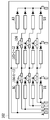
- FIG. 2 is a chip plan view illustrating an electric circuit configuration of the optical signal processing device according to the first embodiment of the present invention.
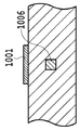
- FIG. 3 is a sectional view of a chip of a phase shifter of the optical signal processing device of FIG. 2.
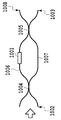
- FIG. 4 is a plan view of an MZI including the phase shifter of FIG. 3.
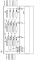
- FIG. 6 is a plan view illustrating a configuration of an optical signal processing device according to a second embodiment of the present invention.
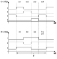
- FIG. 9 is a waveform diagram illustrating a control signal of the optical signal processing device according to the second embodiment.
- FIG. 11 is a plan view illustrating a configuration of an optical signal processing device according to a third embodiment of the present invention.
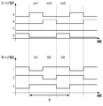
- FIG. 14 is a waveform diagram illustrating an example of a control signal of the optical signal processing device according to the third embodiment.
- FIG. 14 is a waveform diagram illustrating another example of the control signal of the optical signal processing device according to the third embodiment.
- FIG. 14 is a waveform chart illustrating still another example of the control signal of the optical signal processing device according to the third embodiment.
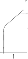
- FIG. 9 is a frequency characteristic diagram illustrating a change in a phase modulation amount of a phase shifter with respect to a switching frequency.
- FIG. 14 is a diagram illustrating an example in which a phase shifter is not arranged at an intersection in a fourth embodiment of the present invention.
- 16 is a constellation map of a 16QAM signal for explaining a fifth embodiment of the present invention.
- FIG. 9 is a diagram illustrating an optical signal of each part of a Mach-Zehnder interferometer including a phase modulation element for explaining a fifth embodiment of the present invention.
- FIG. 16 is a complex signal vector diagram showing a relationship between the optical signals in FIG. 15.
- FIG. 9 is a frequency characteristic diagram illustrating a relationship between a phase modulation amount of a phase modulation element and a time-division driving frequency for explaining a fifth embodiment of the present invention.
- FIG. 2 is a plan view of a chip showing an electric circuit configuration of the optical signal processing device according to the first embodiment of the present invention.
- the optical signal processing device shown in FIG. 2 is, for example, an optical signal processing device having three optical inputs and four optical outputs, and an optical waveguide chip 102 formed on a substrate has a phase of an optical signal passing through an optical waveguide (not shown).
- twelve diodes 104-1 to 104-12 corresponding to each phase shifter are arranged in an array configuration of four rows and three columns as shown in the figure. And are connected by electric wiring.
- four row control signals are supplied from a control unit (not shown) to the electric wiring pads (terminals) A, B, C, and D of the four lower left row control signals.
- the wiring of the four row control signals is divided into two in the row direction at each row position of the first column on the left end, and one of the two branched wirings is connected to the phase shifter on the first column to control the same. , Through the first row of diodes, to the column-driven electric wiring pads (terminals) 1.
- the other of the two lines of the four row control signals which is branched into two, reaches the branch point of the second column at the center via the wire bonding wiring 106 for the other rows directly. .
- the wiring of the four row control signals is further branched in the row direction at each row position.
- One line of the four row control signals branched into two in the center second column is connected to a phase shifter in the second column to control the same, and then passed through a diode in the second column to be connected to a column driving electric wiring.
- the wire is collected on the pad (terminal) 2.
- the other of the two branched lines of the four row control signals is directly connected to the first row through the wire bonding wiring 106 except for the first row, and reaches the rightmost third column.
- the wirings of the four row control signals are connected to the phase shifter in the third column to control the phase shifter, and thereafter, are connected to the column-driving electric wiring pads (terminals) 3 through the diodes in the third column.
- the three column drive electric wiring pads (terminals) 1 to 3 on which the four row control signals (A to D) are condensed are synchronized with the row control signal by a column drive signal from a column drive unit (not shown). Each is time-division driven.
- the control wiring of the row control signal and the column drive signal for accessing the driven element having the phase shifter is shared by the plurality of driven elements, and the optical signal processing is performed by the column drive signal and the row control signal.
- the device can be time-sharing controlled. (Structure of phase shifter)
- FIG. 3 is a cross-sectional view of the chip in a plane orthogonal to the optical waveguides of the phase shifters 103-1 to 103-12.
- the phase shifter constituting the driven element includes a heater 1001 and an optical waveguide 1006 disposed directly below the heater.
- the control signal is applied to both ends of the heater 1001 of the phase shifter to generate heat. An optical effect is generated, and the phase of the optical signal passing through the optical waveguide 1006 in that portion is phase-shift-modulated.
- the optical waveguide 1006 is formed of, for example, a silica-based optical waveguide, a polymer waveguide, silicon, or the like.
- FIG. 3 illustrates the buried waveguide structure as an example, but other structures such as a rib type or a diffusion type may be used.
- FIG. 4 is a plan view of an MZI (Mach-Zehnder interferometer) as an example of a driven element including the phase shifter of FIG.
- the phase shifter of FIG. 3 is provided in the MZI arm optical waveguide 1006 of FIG. That is, the MZI shown in FIG. 4 is arranged as a driven element at each position of the phase shifters 103-1 to 103-12 in FIG.
- an optical signal input from the input optical waveguide 1002 is branched into two by a directional coupler 1004 into arm optical waveguides 1006 and 1007.
- a heater 1001 is provided above one arm optical waveguide 1006 as shown in FIG. 3, and a control signal is applied to phase shift modulate the phase of an optical signal passing through the arm optical waveguide 1006 by a thermo-optic effect.
- the optical signals that have passed through the arm optical waveguides 1006 and 1007 are then multiplexed by the directional coupler 1005, and depending on the phase difference between the two multiplexed optical signals, the MZI output optical waveguide 1003 or 1008. And output.
- an optical element having a function such as an optical switch or an optical attenuator can be configured to be a driven element of the optical signal processing device of the present invention.
- a row control signal (hereinafter referred to as A to D which is the same as the terminal name of the row electrode pad) and a column drive signal (similarly denoted by the terminal names 1 to 3 of the column electrode pad).
- the phase shifters 103-1 to 103-12 selected and accessed in () are arranged and addressed in a matrix, and the rows are represented by letters and the columns are represented by numbers.
- the display order of the rows and columns is arbitrary.
- the phase shifters 103-1 to 103-12 are given priority in the row direction, and are assigned addresses A1 to A3, B1 to B3, C1 to C3, and D1 to D3, respectively. Corresponding. In the drawing, only the addresses A1, A3, D1, and D3 of the phase shifters at the four corners are illustrated for simplicity.
- phase shifter One electrode (the input side of the heater in FIG. 2) of the phase shifter existing in the same row is connected by a horizontal row wiring, and the other electrode (the cathode side of the diode in FIG. 2) is connected by a vertical column wiring. Connect with.
- the phase shifters are arranged in four rows and three columns.
- the crossing of the row wiring and the column wiring is realized by straddling by the wire bonding 106, but another method may be used.
- the electric wiring on the optical waveguide may be straddled by making the electric wiring multi-layered. (Drive of phase shifter)
- a high potential is supplied to the row wiring pad A and a low potential is supplied to the column wiring pad 1 to the phase shifter (A1) in the leftmost column and the topmost row.
- Power is supplied by supplying a potential and generating a potential difference.
- power is supplied to the phase shifter (D3) in the rightmost column and the bottom row by generating a potential difference between the row wiring pad D and the column wiring pad 3.
- diodes 104-1 to 104-12 are attached in series to the electric wiring to each phase shifter, thereby preventing a sneak current and suppressing feeding to an unintended phase shifter.
- This diode may be any element having electric rectification characteristics and rectification means, and a pn junction or a Schottky diode can be used.
- rectifying characteristics can be provided by forming a pn junction in the optical waveguide. (Number of electrical pads, number of wires)
- the number of the electric pads taken out from the chip having the optical waveguide is reduced to seven in comparison with the number of the phase shifters. This is because in the present invention, wiring is shared by rows and columns, and the number of wirings is equal to the number of rows + the number of columns. In the conventional configuration, the number of electrode pads is equal to the number of heaters (the number of rows ⁇ the number of columns). In consideration of the above, a larger effect can be obtained when more phase shifters are used.
- FIG. 5 is a plan view showing an optical switch configured as an optical signal processing device according to the second embodiment of the present invention.
- the optical switch chip 102 is connected to a control signal generator 1010 that generates row control signals (A to D) and column drive signals (1 to 3).
- the control signal generating unit 1010 is a control signal that is time-divisionally synchronized with at least one of the row wiring electric pads A to D and at least one of the column wiring electric pads 1 to 3 so as to address a phase shifter to be controlled.
- FIG. 5 also shows three input fibers 101-1 to 101-3 for providing input optical signals of the optical switch and four output fibers 105-1 to 105-4 for providing output optical signals of the optical switch.
- the optical input terminal and the optical output terminal constitute an input port and an output port of an optical waveguide formed on the substrate of the optical waveguide chip 102.
- the other parts of the second embodiment of FIG. 5 are the same as those of the first embodiment of FIG. (Time waveform of control signal)
- FIG. 6 is a waveform diagram of a control signal output by the control signal generation unit 1010, illustrating a control method of the optical signal processing device (optical switch) according to the second embodiment.
- a to D indicate the potentials of the row electrode pads
- 1 to 3 indicate the potentials of the column electrode pads.
- the time on the time axis is obtained by further dividing the switching cycle T, which is sufficiently shorter than the thermal time constant ⁇ of the phase shifter, into four time slots (slots 1 to 4),
- T which is sufficiently shorter than the thermal time constant ⁇ of the phase shifter
- a time-division control signal is used to change the level synchronously between a high potential and a low potential.
- the row control signals (A to D) have a high potential as a significant signal (positive logic)
- the column drive signals (1 to 3) have a low potential as a significant signal (positive logic). Negative logic).
- FIG. 6 shows the addresses (A1, B2, D3, (C1, C3)) of the phase shifter selected in each of the time slots (slot1 to slot4).
- slot1 In slot1, a high potential is applied only to the electric pad A of the row wiring, and a low potential is applied only to the electric pad 1 of the column wiring. Therefore, in slot1, a potential difference is applied only to phase shifter A1, and phase shifter A1 is addressed.
- a unit of a time waveform of a switching cycle T including a plurality of time slots is a time division control signal in which the row control signals (A to D) and the column drive signals (1 to 3) are synchronized in the time slots.
- the row control signals (A to D) and the column drive signals (1 to 3) are synchronized in the time slots.
- an arbitrary phase shifter can be individually controlled by periodically applying a control signal to a phase shifter to be controlled in a time-sharing manner.
- switching period T the period in which each phase shifter is addressed (switching period T) is set to be sufficiently shorter (T ⁇ ) than the time constant ⁇ of the phase shifter.
- thermo-optic phase shifter in the quartz optical waveguide
- the phase shift given to the optical signal by the phase shifter does not respond within one time slot of the control signal or the switching period T,
- PWM Pulse Width Modulation
- the above-described repetition of the control signal in a predetermined pattern over a plurality of switching periods T means that the time waveform of the control signal in each switching period T is changed in each switching period T as shown in the figure.
- a pattern that repeats with the same time waveform every time may be used, or a pattern that repeats with a different time waveform may be used.
- Such a pattern repeated with different time waveforms can be generated, for example, every time each switching cycle T, by changing the order of time slots cyclically or randomly.
- the period of the pattern is shorter than the time constant of the phase shifter, and it is desirable that the same set of phase shifters be driven the same number of times in the period of the pattern.
- FIG. 7 is a plan view illustrating a configuration of an optical signal processing device (optical switch) according to Embodiment 3 of the present invention.
- the optical signal processing device of the third embodiment is a three-input, four-output optical signal processing device similar to that of the second embodiment (FIG. 5), and the optical switch chip 102 on the substrate has 12 phases.
- Shifters 103-1 to 103-12 and twelve diodes 104-1 to 104-12 corresponding to each phase shifter are arranged in an array configuration of four rows and three columns, and are connected by electric wiring.
- the chip 102 of the optical signal processing device is connected to a control signal generator 1010 that generates a column drive signal (1 to 3) and a row control signal (A to D), and has three input fibers 101-1 to 10-3. It operates as an optical switch for switching and controlling the input optical signal from 101-3 to four output fibers 105-1 to 105-4.
- MZI is described in, for example, FIG. This is realized by connecting a plurality of connections as shown in FIG.
- the output fiber 105 from which the signal light input from the input optical fiber 101 is output is selected according to which phase shifter 103 is driven.
- FIGS. 8 to 10 show waveform diagrams of control signals for explaining the operation of the control signal generator 1010 as a control method of the optical signal processing device of the third embodiment.
- access electric wiring to each phase shifter 103 is provided via row electric pads A to D and column electric pads 1 to 3.
- the phase shifter (A1) in the top row and the leftmost column in FIG. 7 can be supplied with power by generating a potential difference between the row electric pad A and the column electric pad 1, Power can be supplied to the lowermost row and rightmost phase shifter (D3) by generating a potential difference between the row electric pad D and the column electric pad 3.
- the control signal generator 1010 generates and transmits a control signal that generates such a potential difference.
- any signal may be used as long as a signal (potential difference, power, etc.) can be given to each electrode in a time division manner.
- a signal potential difference, power, etc.
- an arbitrary waveform generator can be used to generate and transmit a signal whose potential changes arbitrarily with time.
- GPIO pins of an FPGA, CPU, DSP or the like may be directly connected to the electrode pads A to D and 1 to 3.
- the fixed switching period T is divided into three time slots, and in each of the divided time slots, power is supplied to different phase shifters by time division synchronization control of the control signal generation unit 1010. It can also be done.
- FIG. 8 shows an example of the pad potential waveform of the control signal generated by the control signal generator 1010 when driving the three phase shifters A1, B2, and D3.
- the time waveform of the control signal may be repeated in the same or different predetermined patterns over a plurality of switching periods T. (Phase modulation frequency characteristics and switching frequency)
- the switching period T of the control signal of the phase shifter generated by the control signal generation unit 1010 is a time sufficiently shorter than the time constant ⁇ of the thermal response in which the phase shifter reacts. That is, the switching frequency fs of the control signal is set to a frequency sufficiently higher than the frequency (cutoff frequency fc) corresponding to the time constant ⁇ of the thermal response to which the phase shifter reacts.
- FIG. 11 is a frequency characteristic diagram showing a change in the phase modulation amount of the phase shifter with respect to the switching frequency f.
- the slow switching frequency f f ⁇ fc: cut-off frequency
- the response of the phase shifter follows during one cycle, but the other phase shifters that are simultaneously controlled in a time-sharing manner during that period.
- the control becomes easier (the switching frequency may be lower) when the response time of the driven element is slower (in FIG. 11, the phase modulation amount is attenuated at a higher frequency).
- the thermo-optic effect have a relatively slow response time and are therefore easier to control.
- phase shifter A when supplying power, since a plurality of phase shifters are electrically connected, rectifying means for preventing power from being supplied due to current sneaking into an unintended phase shifter.
- a diode is provided in series with each phase shifter. For example, in FIG. 7, when there is no diode, when driving the phase shifter A1, for example, when applying a high potential to the electric pad A and applying a low potential to the electric pad 1, the electric pad A ⁇ phase A current flows in the order of shifter A2 ⁇ phase shifter B2 ⁇ phase shifter B1 ⁇ electric pad 1, and unexpected phase shifters may be driven.
- a diode is attached to the electric wiring (the wiring of the column drive signals 1 to 3) on the output side of each phase shifter, thereby preventing the current from sneaking and suppressing the power supply to the unintended phase shifter.
- This diode may be provided in the electric wiring (the wiring of the row control signals A to D) on the input side of the phase shifter, may be in the opposite direction if the level of the control signal is inverted, and may be an element having rectification characteristics.
- a pn junction or a Schottky diode can be used.
- a switching diode having a short reverse recovery time is used.
- rectifying characteristics can be provided by forming a pn junction in the optical waveguide.
- phase shifters having the same row or column can be simultaneously driven in the same slot.
- FIGS. 9 and 10 are other examples of waveform diagrams of the control signal generated by the control signal generation unit 1010 during the time division control in which the switching period T is divided into three time slots.
- a potential difference is applied to the phase shifters A1 and A2 in the same row A in slot 1, a potential difference to B2 in slot 2, and a potential difference to D3 in slot 3.
- a potential difference is applied to A1 and C1 in the same row 1 in slot 1, B2 in slot 2, and D3 in slot 3.
- Both the examples shown in FIGS. 9 and 10 are examples in which a plurality of phase shifters are driven at the same timing in slot 1, but other slots 2 and 3 may be used.
- a plurality of phase shifters existing in the same row or the same column can be simultaneously controlled in a single slot. It can be driven to control the optical switch.
- one switch element may be driven by one phase shifter, or one switch element may be driven by a plurality of phase shifters.
- the number of time division slots can be reduced by simultaneously driving the phase shifters used to drive one switch element.
- the time waveform of the control signal may be repeated in the same or different predetermined patterns over a plurality of switching periods T.
- Examples of the optical signal processing device capable of performing such control include a matrix switch and a multicast switch using a plurality of phase shifters, a lattice filter, a transversal filter, and a variable optical attenuator array. (Example 4)
- the wiring to the phase shifter is constituted by a row (row) and a column wiring to form a matrix, thereby realizing control of each phase shifter with less electric wiring.
- the electric wires need not be physically wired in a matrix, but may be logically arranged in a matrix as an equivalent circuit.
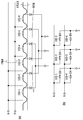
- FIG. 12A is a diagram illustrating an example of a physical circuit configuration of a lattice filter according to Embodiment 4 of the present invention
- FIG. 12B is a diagram illustrating an electrical equivalent circuit of FIG.
- the physical characteristics of the actual optical waveguide on the optical waveguide substrate, the phase shifters 103-1 to 103-6, and the electric wiring (row wirings A and B and column wirings 1 to 3) for controlling the phase shifter are shown.
- 2 shows a typical layout.
- FIG. 12A also shows a diode as a rectifier.
- the lattice filter has been described as an example.
- the present invention is also applicable to a transversal filter, a filter using a ring resonator, a variable optical attenuator array using MZI, and an optical signal processing device combining them.
- the invention is applicable.
- the present invention can be applied to the optical switches shown in the first to fourth embodiments.
- FIG. 13 shows an example in which the phase shifter 103-5 is not arranged at the intersection of the row wiring B and the column wiring 2.
- the access wiring is developed two-dimensionally, and it is apparent that it is not necessary to form a strict matrix. That is, the matrix (array, array, matrix) in the present invention may include a partially vacant element, and the access wiring can be developed as a whole even in a coarse (sparse) array. Good if possible. (Example 5)
- a time-division driving frequency fs (frequency corresponding to the switching period T in the first to third embodiments) when performing time-division access to each driven element will be examined.
- phase modulation element In recent optical communication systems, signals are generally transmitted using a quadrature amplitude modulation (QAM) format in order to increase the frequency use efficiency.
- QAM quadrature amplitude modulation
- the generation of the QAM signal requires a phase modulation element.
- the driven element is a phase modulation element and the time division drive frequency fs is not sufficiently high, the phase modulation component of the phase modulation element due to the time division drive signal is As noise, it is superimposed on the optically modulated QAM signal and may degrade communication quality. Therefore, it is preferable that the time division driving frequency is sufficiently higher than the response of the phase modulation element.
- FIGS. 14 to 17 are conceptual diagrams illustrating the fifth embodiment based on the above concept.
- a 16 QAM signal will be described as an example.
- QPSK Quadrature Phase Shift Keying
- 64 QAM 64 QAM.
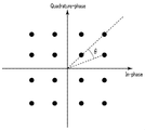
- FIG. 14 is a constellation map of a 16QAM signal. Each symbol point corresponds to information, and it is important that they are well separated for accurate communication.
- FIG. 15 is a diagram showing optical signals of various parts of the Mach-Zehnder interferometer including the phase modulation element 153 of the optical signal processing device described in the fifth embodiment.
- an input optical signal Ein is split into two by a coupler 151, one of which is phase-modulated by a phase modulation element 153, which is a phase shifter, then multiplexed via a coupler 152 and output as Eout. .
- which of the two outputs is output is determined based on the phase relationship between the two branched optical signals E1 and E2.
- the optical signal E2 is modulated by the phase modulation element (phase shifter) 153.
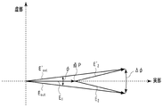
- the driving frequency component remaining in E2 is shown in the complex signal vector diagram of FIG. To be superimposed on the modulated optical signal. That is, the optical electric field Eout after the Mach-Zehnder output of the optical signal is obtained by vector-combining the optical electric field E2 via the arm having the phase modulation element with the end point P on the phasor of the optical electric field E1 via the arm to which no phase modulation is applied. And Eout undergoes phase modulation by the residual phase component ⁇ provided by the phase modulation element.
- the phase modulation amount given by the output optical signal is a phase amount indicated by a superimposed phase ⁇ in FIG.
- the frequency fs of the time division drive is set sufficiently higher than the response frequency fc of the phase modulation element, ⁇ ⁇ It is preferred that Preferably, ⁇ ⁇ 0.1 ⁇ ⁇ (1) And set.
- FIG. 17 is a frequency characteristic diagram showing the relationship between the frequency response (cutoff frequency fc corresponding to the time constant ⁇ ) of the phase modulation element, the residual phase ⁇ , and the time division drive frequency fs.
- an optical signal processing device such as an optical switch or an optical filter realized using an optical waveguide
- REFERENCE SIGNS LIST 100 electric wiring 200 electric pad 102 optical waveguide chip 103-1 to 103-12 phase shifter 104-1 to 104-12 diode A to D electric wiring pad (row control signal terminal) 1-3 Electric wiring pads (column drive signal terminals) 106 Wire bonding wiring 101-1 to 101-3 Input fiber 105-1 to 105-4 Output fiber 153 Phase modulation element 1001 Heater 1002 Input optical waveguide 1003, 1008 Output optical waveguide 1004, 1005, 151, 152 Directional coupler ( Coupler) 1006, 1007 (arm) optical waveguide 1010 control signal generator
Landscapes
- Physics & Mathematics (AREA)
- Nonlinear Science (AREA)
- General Physics & Mathematics (AREA)
- Optics & Photonics (AREA)
- Engineering & Computer Science (AREA)
- Computer Networks & Wireless Communication (AREA)
- Optical Modulation, Optical Deflection, Nonlinear Optics, Optical Demodulation, Optical Logic Elements (AREA)
Abstract
光導波路を用いて実現される光スイッチや光フィルタ等の光信号処理装置における電気配線を削減する。基板上に形成された光導波路を有する光信号処理装置であって、前記光導波路は少なくとも一つの入力ポートと、少なくとも一つの出力ポートを有し、前記入力ポートから入力された光信号に対して位相シフトを加える位相シフタを含む被駆動エレメントを複数有し、各前記被駆動エレメントは少なくとも二つの制御端子を有し、前記二つの制御端子間に時分割同期した制御信号を印加する制御配線を有し、前記被駆動エレメントへアクセスする前記制御配線が複数の被駆動エレメントで共有される光信号処理装置とした。
Description
本発明は、光導波路により構成される光信号処理装置、とくに外部から電気制御信号を印加してその状態を変えることが可能な光信号処理装置、およびその制御方法に関する。
光導波路は、光を微小な領域に閉じ込めて制御することで様々な機能を発現する技術として、種々の光デバイスに使用されている。光導波路は一般的に、石英系材料、ポリマ、ニオブ酸リチウムなどの各種誘電体やシリコン(Si)、インジウム燐(InP)、などの半導体材料により構成される。
光導波路技術を用いたデバイスとして、熱光学効果(温度による屈折率の変化)を用いた光スイッチや光可変減衰器などがある。例えば、光スイッチであれば、熱光学効果を用いた位相シフタを有するマッハツェンダ干渉計(Mach-Zehnder Interferometer:MZI)(非特許文献1)を複数、直列および並列に組み合わせ配列構成することで、多入力多出力スイッチが実現できることが報告されている(非特許文献2、3)。この光スイッチでは、各MZIの位相シフタを電気信号で駆動して熱光学効果で位相変化させることにより、多数の入力光の出力先をスイッチングすることができる。
また、光可変減衰器(Variable Optical Attenuator:VOA、非特許文献4)も報告されており、例えばMZIを、位相シフタとともに複数集積することで、光可変減衰器をアレイ化することも可能である。
上述のような光導波路を用いた種々の光デバイスは、光通信システムの構成に不可欠であり、とくに近年のCDC(Colorless、Directionless,Contentionless)-ROADM(Reconfigurable Optical Add/Drop Multiplexing)機能を有する光通信ノードにおいて、その重要性を増している。例えば、マルチキャストスイッチ(MultiCast Switch:MCS)は、CDC-ROADM機能を実現するのに不可欠な光デバイスである。MCSのようなデバイスは、熱光学効果を用いた位相シフタにより、電気信号で光信号のスイッチ状態を変更するが、ROADM装置すなわち光ノードの規模が大きくなるにつれて、内包する位相シフタの数が増大する。
例えば、16x16規模のMCSでは、スイッチエレメントの数は少なくとも256個以上になる。光信号のオフ状態での消光比を確保するため、一つのスイッチエレメント(被駆動エレメント)は2つのMZIで構成する方式が好ましく、位相シフタの数は512個にも及ぶこととなる。
T. Shibata et al., "Silica-Based Waveguide-Type 16 x 16 Optical Switch Module Incorporating Driving Circuits", in IEEE Photonics Technology Letters, vol. 15, no. 9, pp. 1300-1302, Sept. 2003.
Takashi Goh, Mitsuho Yasu, Kuninori Hattori, Akira Himeno, Masayuki Okuno, and Yasuji Ohmori, "Low Loss and High Extinction Ratio Strictly Nonblocking 16×16 Thermooptic Matrix Switch on 6-in Wafer Using Silica-Based Planar Lightwave Circuit Technology", IEEE J. Lightwave Technol., vol. 19, no. 3, pp.371-379, 2001
T. Watanabe, et. al., "Silica-based PLC Transponder Aggregateors for Colorless, Directionless, and Contentionless ROADM", OFC/NFOEC2012, OTh3D.1, March 8, 2012, Los Angeles
Kei Watanabe, Yasuaki Hashizume, Yusuke Nasu, Masaki Kohtoku, Mikitaka Itoh, and Yasuyuki Inoue, "Ultralow Power Consumption Silica-Based PLC-VOA/Switches", J. Lightwave Technol. 26, 2235-2244 (2008)
上述のMCSでは、512個のMZIを駆動するために、各MZIが有する位相シフタに対して、それぞれ制御電気信号を印加する必要がある。従来のMCSなどの光スイッチデバイスでは、各位相シフタからチップ端まで電気配線をチップ上に形成し、チップ端からボンディングパッドを介してプリント基板(ワイヤボンディング基板)へワイヤボンディングすることで、各位相シフタへの制御電気信号のアクセスを行っていた。しかしながら、従来の方法ではチップ上に電気配線やボンディングパッドが占める面積が大きくなり、チップ面積が増大するという課題を有していた。電気配線の面積は、デバイスの規模が大きくなるほど顕著であり、例えば、図1に示す従来の16x16程度の規模のMCSチップであっても、チップ面積の半分は制御用の512本の電気配線100および電気パッド200に起因する面積で占められる(非特許文献2のFig.3.より)。
本発明は、このような問題に鑑みてなされたものである。その目的とするところは、チップ基板上に形成された光導波路を有する光信号処理装置において、チップ内の位相シフタなどの被駆動エレメントへアクセスする電気配線を、等価回路的に少なくとも2次元のマトリックス状に構築することにより、制御回路に接続するために必要なワイヤボンディング用電気パッドの個数を削減し、電気配線を簡易化することにある。
本発明は、このような目的を達成するために、以下のような構成を備えることを特徴とする。
すなわち本発明は、基板上に形成された光導波路を有する光信号処理装置であって、光導波路は少なくとも一つの入力ポートと、少なくとも一つの出力ポートを有し、入力ポートから入力された光信号に対して位相シフトを加える位相シフタを含む被駆動エレメントを複数有し、各被駆動エレメントは少なくとも二つの制御端子を有する位相シフタを含む光導波路型の光デバイスであって、複数の被駆動エレメントを等価回路的に行列(アレイ、マトリックス)に配列し、同一の行に存在する各被駆動エレメントの一方の端子同士を電気的に接続する行配線と、同一の列に存在する各被駆動エレメントの他方の端子同士を電気的に接続する列配線を設け、行配線もしくは列配線のうち少なくとも一方を、電気的駆動手段で駆動ないし制御する光信号処理装置である。
また、複数の被駆動エレメント(素子)を駆動する制御方法としては、電気的駆動手段は列の数だけ存在し、各電気的駆動手段を時分割で列駆動するとともに、各行配線に列駆動状態に同期して行制御信号を印加することで被駆動エレメントを個別に制御する制御方法であり、列駆動信号と行制御信号で光信号処理装置を時分割制御する。ここで列駆動信号と行制御信号は合せて制御信号と総称することができ、行配線、列配線も同様に制御配線ということができる。
なお、行列やアレイ、マトリックス、配列の表現として一般的なことであるが、配列等の次元は2次元に限らず、各次元の表記の順番は置換可能、すなわち例えば2次元の場合の行と列を入れ替えても同等な構成を実現可能であることは自明である。
以下の説明では主にチップ(基板)平面上における行と列の2次元配列の構成を例に説明するが、本発明では例えば複数枚のチップを集積し実装して、3次元配列の光信号処理装置とすることもでき、さらにそのような3次元配列の光信号処理装置を単位として複数配列して3次元以上の多次元の配列としても構成が可能である。以下の説明に於ける行や列のなどの表現は、2次元配列の場合はもとより、3次元以上の多次元配列の構成における2次元部分配列についてのものとしても理解されるべきである。
また被駆動エレメント(素子)としてはスイッチング素子に限ることは無く、少なくとも独立な2つ以上の制御信号入力(端子、パッド)を有し位相シフタを有する素子であれば良い。更に、被駆動エレメントは必ずしも物理的に行列、アレイ、マトリックス状に配列されていることも必要ではなく、等価回路的にそのような配列として独立な少なくとも2つ以上の方向からアクセス可能であれば本発明は適用可能である。
本発明の実施形態の構成の一例は下記の通りである。
(構成1)
(構成1)
基板に形成された光導波路を有する光信号処理装置であって、
前記光導波路は少なくとも一つの入力ポートと、少なくとも一つの出力ポートを有し、
前記入力ポートから入力された光信号に対して位相シフトを加える位相シフタを含む被駆動エレメントを複数有し、
各前記被駆動エレメントは少なくとも二つの制御端子を有し、
前記二つの制御端子間に時分割同期した制御信号を印加する制御配線を有し、
前記被駆動エレメントへアクセスする前記制御配線が複数の被駆動エレメントで共有される
ことを特徴とする光信号処理装置。
(構成2)
前記光導波路は少なくとも一つの入力ポートと、少なくとも一つの出力ポートを有し、
前記入力ポートから入力された光信号に対して位相シフトを加える位相シフタを含む被駆動エレメントを複数有し、
各前記被駆動エレメントは少なくとも二つの制御端子を有し、
前記二つの制御端子間に時分割同期した制御信号を印加する制御配線を有し、
前記被駆動エレメントへアクセスする前記制御配線が複数の被駆動エレメントで共有される
ことを特徴とする光信号処理装置。
(構成2)
前記複数の被駆動エレメントは等価回路的にマトリックスに配置され、
前記制御配線は、前記マトリックスの行に対応する行制御配線と前記マトリックスの列に対応する列駆動配線とを有し、行および列の交点に前記被駆動エレメントが存在する場合には、その前記二つの制御端子が前記行制御配線と列駆動配線に接続される
ことを特徴とする構成1に記載の光信号処理装置。
(構成3)
前記制御配線は、前記マトリックスの行に対応する行制御配線と前記マトリックスの列に対応する列駆動配線とを有し、行および列の交点に前記被駆動エレメントが存在する場合には、その前記二つの制御端子が前記行制御配線と列駆動配線に接続される
ことを特徴とする構成1に記載の光信号処理装置。
(構成3)
前記行制御配線の各々と、前記列駆動配線の各々とに接続され、少なくとも一つの所望の被駆動エレメントに接続された前記行制御配線および前記列駆動配線を選択的にアドレスする時分割同期した前記制御信号を発生する制御信号発生手段を有する
ことを特徴とする構成2に記載の光信号処理装置。
(構成4)
ことを特徴とする構成2に記載の光信号処理装置。
(構成4)
前記被駆動エレメントの各々に対して直列に接続された整流手段を有する
ことを特徴とする構成1から3のいずれかに記載の光信号処理装置。
(構成5)
ことを特徴とする構成1から3のいずれかに記載の光信号処理装置。
(構成5)
前記光信号処理装置は、マトリックススイッチ、マルチキャストスイッチ、もしくは光フィルタまたは光信号減衰器アレイである
ことを特徴とする構成1から4のいずれか1項に記載の光信号処理装置。
(構成6)
ことを特徴とする構成1から4のいずれか1項に記載の光信号処理装置。
(構成6)
前記制御信号は、所定の時間スロットで時分割同期した時間波形の時分割制御信号であり、複数の時間スロットを含む切替周期Tの複数の前記切替周期Tにわたって前記時間波形が所定のパターンで反復される制御信号である
ことを特徴とする構成1から5のいずれかに記載の光信号処理装置の制御方法。
(構成7)
ことを特徴とする構成1から5のいずれかに記載の光信号処理装置の制御方法。
(構成7)
前記時分割制御信号の切替周期Tは、前記位相シフタの時定数τよりも十分短い
ことを特徴とする構成6に記載の光信号処理装置の制御方法。
(構成8)
ことを特徴とする構成6に記載の光信号処理装置の制御方法。
(構成8)
前記光信号の変調フォーマットが直交振幅変調信号であって、
前記直交振幅変調信号の各シンボル点間の距離に相当する位相差θとし、前記位相シフタの周波数応答における、前記時分割制御信号の切替周波数fs(=1/T)での残留変動成分をψとするとき、
ψ<θ
である
ことを特徴とする構成6または7に記載の光信号処理装置の制御方法。
前記直交振幅変調信号の各シンボル点間の距離に相当する位相差θとし、前記位相シフタの周波数応答における、前記時分割制御信号の切替周波数fs(=1/T)での残留変動成分をψとするとき、
ψ<θ
である
ことを特徴とする構成6または7に記載の光信号処理装置の制御方法。
本発明によれば光導波路を用いて実現される光スイッチや光フィルタ等の光信号処理装置における電気配線を削減することができ、チップサイズの削減が可能である。加えて、従来個別の被駆動エレメント毎に設置していた電源等の駆動手段を、複数の被駆動エレメントを異なる時間タイミングで時分割して、行、列などの単位で共有することで、駆動手段の数を削減することが可能である。上記の効果により、光信号処理装置のチップサイズを削減し、量産性を向上し、部品点数の削減を通じて装置の低廉化に寄与する。
以下、図面を参照しながら本発明の実施形態について詳細に説明する。
(実施例1)
(実施例1)
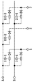
図2は、本発明の実施例1の光信号処理装置の電気回路構成を示すチップ平面図である。図2の光信号処理装置は、例えば3光入力、4光出力の光信号処理装置であって、基板上に形成された光導波路チップ102には、図示しない光導波路を通過する光信号の位相を変化させる12個の位相シフタ103-1~103-12、および各位相シフタに対応する12個のダイオード104-1~104-12が、図示のように4行3列のアレイ構成で配置されて、電気配線で接続されている。
図2において、左下の4つの行制御信号の電気配線パッド(端子)A,B,C,Dには、図示しない制御部から4つの行制御信号が供給されている。4つの行制御信号の配線は、左端の1列目のそれぞれの行位置で行方向に2分岐され、2分岐された一方の配線は1列目の位相シフタに接続されてこれを制御した後、1列目のダイオードを経て、列駆動の電気配線パッド(端子)1に集線される。
左端の1列目において、4つの行制御信号の2分岐された他方の配線は、1行目は直接、1行目以外はワイヤボンディング配線106を経て、中央の2列目の分岐点に至る。2列目の分岐点において4つの行制御信号の配線は、それぞれの行位置で行方向にさらに2分岐される。
中央の2列目において2分岐された4つの行制御信号の一方の配線は、2列目の位相シフタに接続されてこれを制御した後、2列目のダイオードを経て、列駆動の電気配線パッド(端子)2に集線される。
同様に、2列目において、4つの行制御信号の2分岐された他方の配線は、1行目は直接、1行目以外はワイヤボンディング配線106を経て、右端の3列目に至る。4つの行制御信号の配線は、3列目の位相シフタに接続されてこれを制御した後、3列目のダイオードを経て、列駆動の電気配線パッド(端子)3に集線される。
4つの行制御信号(A~D)が集線された3つの列駆動の電気配線パッド(端子)1~3は、図示しない列駆動手段からの列駆動信号により、行制御信号と同期して、それぞれ時分割駆動されている。
このような構成により、位相シフタを有する被駆動エレメントへアクセスする行制御信号や列駆動信号の制御配線が、複数の被駆動エレメントで共有されており、列駆動信号と行制御信号で光信号処理装置を時分割制御することができる。
(位相シフタの構造)
(位相シフタの構造)
図3には、位相シフタ103-1~103-12の光導波路に直交する面におけるチップ断面図を示す。被駆動エレメントを構成する位相シフタは、ヒータ1001とその直下に配置された光導波路1006からなり、位相シフタのヒータ1001の両端に制御信号を印加することで発熱し、直下の光導波路1006に熱光学効果を生じて、当該部分の光導波路1006を通過する光信号の位相が位相シフト変調される。
光導波路1006は、例えば、石英系光導波路、ポリマ導波路、シリコン等により形成される。図3では埋め込み導波路構造を例として説明するが、リブ型や拡散型などの他の構造でも構わない。
図4は、図3の位相シフタを含む被駆動エレメントの一例としてのMZI(マッハツェンダ干渉計)の平面図である。図3の位相シフタは、図4のMZIのアーム光導波路1006に設けられている。すなわち、図2の位相シフタ103-1~103-12の各々の箇所には、図4に示すMZIが被駆動エレメントとして配置されている。
MZIにおいては、その入力光導波路1002から入力された光信号が、方向性結合器1004によりアーム光導波路1006および1007に2分岐される。一方のアーム光導波路1006の上部には、図3のようにヒータ1001が設置されており、制御信号が印加されて熱光学効果によりアーム光導波路1006を通過する光信号の位相を位相シフト変調する。アーム光導波路1006および1007を経由した光信号は、次に、方向性結合器1005により合波され、合波される2つの光信号間の位相差に応じて、MZIの出力光導波路1003もしくは1008に分配されて出力される。
このような位相シフタを含むMZIを用いて、光スイッチや光減衰器などの機能を有する光素子を構成して、本願発明の光信号処理装置の被駆動エレメントとすることができる。
(位相シフタのアドレス)
(位相シフタのアドレス)
図2以下の本発明の実施例では、行制御信号(以下、行電極パッドの端子名と同じA~Dで示す)と列駆動信号(同様に、列電極パッドの端子名1~3で示す)で選択アクセスされる位相シフタ103-1~103-12を、行列状に配置してアドレス付けし、行をアルファベットで、列を数字で表している。行と列の表示の順番は任意であるが、例えば位相シフタ103-1~103-12が行方向優先の順で、それぞれA1~A3、B1~B3、C1~C3、D1~D3のアドレスに対応する。図では簡明に表現するため、四隅の位相シフタのアドレスA1、A3、D1、D3のみを例示している。
同一の行に存在する位相シフタの一方の電極(図2ではヒータの入力側)を横方向の行配線で接続し、他方の電極(図2ではダイオードのカソード側)同士を縦方向の列配線で接続する。本構成では、4行3列に位相シフタを配列している。
図2では、行配線と列配線の交差をワイヤボンディング106によって跨ぐことで実現しているが、他の方法を用いても構わない。例えば、光導波路上の電気配線を多層化することにより配線を跨いでもよい。
(位相シフタの駆動)
(位相シフタの駆動)
図2に示す光信号処理装置において、例えば、一番左の列かつ一番上の行の位相シフタ(A1)には、行配線用パッドAに高電位を供給し列配線用パッド1に低電位を供給して、電位差を発生させることで給電する。同様に、一番右の列かつ一番下の行の位相シフタ(D3)には、行配線用パッドDと列配線用パッド3の間に電位差を発生させることで給電する。
位相シフタに電力を供給する際には、複数の位相シフタが電気的に接続されていることから、意図しない位相シフタにも電流が回り込むことで、電力が供給されてしまう可能性がある。これを防止するため、各位相シフタへの電気配線に直列にダイオード104-1~104-12を付けることで、回り込む電流を防止し、意図しない位相シフタに給電することを抑止する。このダイオードは電気的整流特性のある素子、整流手段であればよく、pn接合やショットキーダイオードを使用することが可能である。また、シリコン導波路やInP導波路などの半導体材料による光導波路においては、光導波路内にpn接合を作りこむことで、整流特性を持たせることもできる。
(電気パッド数、配線数)
(電気パッド数、配線数)
上記のように電気配線を行うことにより、本実施例1では光導波路を有するチップから取り出される電気パッドの数は、位相シフタの数12に対して、7に削減される。これは、本発明では配線は行と列で共有され、配線数=行数+列数になるためであり、従来の構成では、電極パッド数がヒータ数と等しい(行数×列数)ことを考えると、より多くの位相シフタを使用する場合にはより大きな効果が得られる。
更に別の数値例で示すと、行方向に20、列方向に5の位相シフタが存在する場合、従来の配線方法では、20×5=100の配線が必要であったのに対して、本発明では制御配線が共有される結果、20+5=25と顕著な配線削減効果が得られる。
また、行と列は可能な限り同数となるように行列を設定するのが、配線数を最小にする点で好ましい。制御すべき位相シフタの数をKとする場合、行配線数Mと列配線数Nとしたとき、
K=M×N
の関係がある。配線数M+Nの最小値はM=Nのときに実現され、このときの配線数は2×K1/2である。例えば、256個の位相シフタを有する場合、M=N=16として配線数は行配線、列配線合わせて32本設置する場合がもっとも配線数が少なく、配線面積削減に効果がある。
(実施例2)
K=M×N
の関係がある。配線数M+Nの最小値はM=Nのときに実現され、このときの配線数は2×K1/2である。例えば、256個の位相シフタを有する場合、M=N=16として配線数は行配線、列配線合わせて32本設置する場合がもっとも配線数が少なく、配線面積削減に効果がある。
(実施例2)
図5は、本発明の実施例2の光信号処理装置として構成した光スイッチを示す平面図である。図5に示すように、光スイッチのチップ102は、行制御信号(A~D)と列駆動信号(1~3)を生成する制御信号発生部1010へと接続されている。制御信号発生部1010は、制御したい位相シフタをアドレスするように行配線電気パッドA~Dのうち少なくとも一つと、列配線電気パッド1~3のうち少なくとも一つに、時分割で同期した制御信号として行制御信号(A~D)と列駆動信号(1~3)を与える。
図5には、光スイッチの入力光信号を与える3本の入力ファイバ101-1~101-3、光スイッチの出力光信号を与える4本の出力ファイバ105-1~105-4も示されており、それぞれの光入力端、光出力端が、光導波路チップ102の基板に形成された光導波路の入力ポート、出力ポートを構成している。図5の実施例2のその他の部分は、図2の実施例1と同じであるので説明を省略する。
(制御信号の時間波形)
(制御信号の時間波形)
図6は、実施例2の光信号処理装置(光スイッチ)の制御方法を説明する、制御信号発生部1010が出力する制御信号の波形図である。図6で、A~Dが行電極パッドの電位、1~3が列電極パッドの電位を示す。
図6では、時間軸(横軸)の時刻は、位相シフタの熱時定数τよりも十分短い切替周期Tを更に4つの時間スロット(slot1~4)に分けて、複数の制御信号の時間波形のレベルを高電位と低電位の間で同期して変化させる時分割制御信号とした例について説明する。図5のダイオードの導通する向きから明らかなように、行制御信号(A~D)は高電位が有意信号(正論理)であり、列駆動信号(1~3)は低電位が有意信号(負論理)である。図6には、各時間スロット(slot1~4)で選択される位相シフタのアドレス(A1,B2,D3,(C1,C3))を示している。
slot1においては、行配線のうち電気パッドAのみに対して高電位を与え、列配線のうち電気パッド1のみに低電位を与える。したがって、slot1においては、位相シフタA1のみに電位差が印加され、位相シフタA1がアドレスされる。
slot2においては、行配線のうち電気パッドBのみに対して高電位を与え、列配線のうち電気パッド2に低電位を与える。したがって、slot2においては、位相シフタB2のみに電位差が印加され、位相シフタB2がアドレスされる。
slot3においては、行配線のうち電気パッドDのみに対して高電位を与え、列配線のうち電気パッド3に低電位を与える。したがって、slot3おいては、位相シフタD3のみに電位差が印加され、位相シフタD3がアドレスされる。
slot4においては、行配線のうち電気パッドCのみに対して高電位を与え、列配線のうち電気パッド1および3に低電位を与える。したがって、slot4においては、位相シフタC1とC3に電位差が印加され、位相シフタC1およびC3がアドレスされる。
このような時間波形で、行制御信号(A~D)と列駆動信号(1~3)が時間スロットで同期した時分割制御信号として、複数の時間スロットを含む切替周期Tの時間波形の単位で反復して光信号処理装置のチップ102の電極パッドに印加されて、各位相シフタを制御する。
上述のように、制御したい位相シフタに対して時分割同期して周期的に制御信号を印加することで、任意の位相シフタを個別に制御することが可能である。ここで各位相シフタがアドレスされる周期(切替周期T)は位相シフタの時定数τよりも十分短く(T<τ)設定する。
例えば、石英系光導波路における熱光学位相シフタの時定数は数ms程度であるから、切替周波数(fs=1/T)を数10~数100kHzとする。位相シフタが光信号に与える位相シフトは熱光学的に作用するため、位相シフタのヒータの発生する熱に対して時定数を持って作用する。位相シフタの熱変化の時定数は電気信号の時定数に比べ十分長いため、制御信号の1つの時間スロットないし切替周期Tの時間内には位相シフタが光信号に与える位相シフトは応答しないが、複数の切替周期Tにわたって所定のパターンで時間波形を反復することによって、制御信号の時間波形の直流成分(実効値)のみがいわばPWM(パルス幅変調)的に積分されて熱光学作用して、アドレス選択された位相シフタの位相シフトに寄与する。
なお、上記で制御信号を、複数の切替周期Tにわたって所定のパターンで反復するというのは、図示のように各切替周期T内の制御信号の時間波形が、反復される各切替周期Tにおいて、毎回同じ時間波形で繰り返すパターンであっても良いが、異なる時間波形で繰り返すパターンであっても良い。このような異なる時間波形で繰り返すパターンは、例えば各切替周期T毎に毎回、時間スロットの順番を巡回的に、あるいはランダムに入れ替えるなどして生成することができる。
この場合でも、パターンの周期は、位相シフタの時定数よりは短いのが望ましく、パターンの周期において、同じ位相シフタの組が同じ回数だけ駆動されるようにするのが望ましい。
この様に制御することで、限られた数の電気配線によって、配列された全ての位相シフタの位相シフトを、熱変化の時定数の範囲内で自在に制御することが可能となる。単純に、選択された位相シフタが熱応答して位相変化を起こすまで待ってから制御信号を切り替えていたのでは、単に制御信号の切り替えが遅くなるのみならず、その間にアドレス選択されていない他の位相シフタが熱応答(温度低下)して位相変化を起こしてしまい、全ての位相シフタの自在な制御は実現できない。
また、slot1~3のように、特定の時間スロットにおいては単一の位相シフタを選択してアドレスすることも可能であるし、slot4のように、同じ行または列における複数の位相シフタを同時にアドレス選択することも可能である。制御すべき位相シフタの数に応じて、切替周期Tに含まれる時間スロットの数を増やし、あるいは減らして変更することも可能である。
(実施例3)
(実施例3)
図7は、本発明の実施例3の光信号処理装置(光スイッチ)の構成を示す平面図である。本実施例3の光信号処理装置は実施例2(図5)と同様な3光入力、4光出力の光信号処理装置であって、基板上の光スイッチチップ102には、12個の位相シフタ103-1~103-12、および各位相シフタに対応する12個のダイオード104-1~104-12が、4行3列のアレイ構成で配置されて、電気配線で接続されている。
光信号処理装置のチップ102は、列駆動信号(1~3)と行制御信号(A~D)を生成する制御信号発生部1010へと接続されており、3本の入力ファイバ101-1~101-3からの入力光信号を、4本の出力ファイバ105-1~105-4へ切り替え制御する光スイッチとして動作する。
一般に、光導波路を用いた多入力多出力光スイッチでは、MZIを例えば非特許文献2のFig.1にあるように複数接続していくことにより実現される。図7のスイッチでは、入力光ファイバ101から入力された信号光が、どの出力ファイバ105から出力されるかを、どの位相シフタ103を駆動するかにより選択する。本実施例3のスイッチは、3入力4出力のスイッチであるため、入出力間の1対1接続のスイッチ状態としては3x4=12通り存在する。12通りの状態を独立に設定するためには、12の自由度が必要であり、12個の位相シフタを独立して制御する必要がある。
(制御方法と制御信号の波形例)
(制御方法と制御信号の波形例)
図8から図10に、本実施例3の光信号処理装置の制御方法として、制御信号発生部1010の動作を説明する制御信号の波形図を例示する。
図7の実施例3においても、実施例2(図5)で示したと同様の構造により、各位相シフタ103へのアクセス電気配線は、行電気パッドA~Dおよび列電気パッド1~3を介して制御信号発生部1010へと接続される。
上記構成により、例えば、図7の一番上の行かつ一番左の列の位相シフタ(A1)には、行電気パッドAと列電気パッド1の間に電位差を発生することで給電でき、一番下の行かつ一番右の位相シフタ(D3)には、行電気パッドDと列電気パッド3の間に電位差を発生することで給電できる。制御信号発生部1010は、このような電位差を発生する制御信号を生成・送信する。
制御信号発生部1010では、各電極に時分割で信号(電位差、電力等)を与えることが可能であれば、どのようなものを使用しても構わない。例えば、図6のような2値パルス波形に限らず任意波形発生器を用いて、時間的に電位が任意に変化するような信号を生成・送信することもできる。また、FPGA、CPU、DSPなどのGPIOピンを直接電極パッドA~D、1~3に接続しても構わない。
このとき、駆動する必要のある位相シフタに対し、時間を分割して順次給電する。例えば、図8に示すように一定の切替周期Tを3つの時間スロットに分割し、分割された各時間スロットでは、制御信号発生部1010の時分割同期制御により異なる位相シフタに給電するように動作させることもできる。図8では、A1,B2,D3の3つの位相シフタを駆動する際の制御信号発生部1010の発生する制御信号のパッド電位波形の一例を示す。実施例2と同様に、制御信号の時間波形を、複数の切替周期Tにわたって同一又は異なる所定のパターンで反復してもよい。
(位相変調量の周波数特性と切替周波数)
(位相変調量の周波数特性と切替周波数)
制御信号発生部1010が生成する位相シフタの制御信号の切替周期Tは、位相シフタが反応する熱応答の時定数τよりも充分に短い時間とする。すなわち制御信号の切替周波数fsは、位相シフタが反応する熱応答の時定数τに対応する周波数(カットオフ周波数fc)よりも充分に高い周波数で行う。
図11は、切替の周波数fに対する位相シフタの位相変調量の変化を表す周波数特性図である。ゆっくりとした切替の周波数f(f<fc:カットオフ周波数)の場合には、位相シフタの応答が1周期の間で追従するものの、その間に時分割で同時に制御している他の位相シフタの位相が変動してしまう。そのため、位相シフタの位相が変動しない程度に高い周波数で切り替えを行う(fc<fs=1/T)ことにより、時分割で制御する複数の位相シフタに対して、同時に電力を供給することができ、それぞれを駆動することができる。
時分割制御を行うに当たり、被駆動エレメントの応答時間は遅い(図11において、高い周波数では位相変調量が減衰する)ほうが制御が容易になる(切替周波数が低くてもよくなる)。熱光学効果を用いた被駆動エレメントは比較的応答時間が遅く、したがって、制御が容易である。
熱光学効果を用いた位相シフタのほかにも、磁気光学効果による偏波変調素子や、高速な応答を示す電気光学効果による光学変調素子においても、各被駆動エレメントに対してコンデンサ等を設置することで応答時間を等価的に長くすることで、本発明の効果を得ることが可能である。
(整流手段)
(整流手段)
また、電力を供給する際には、複数の位相シフタが電気的に接続されていることから、意図しない位相シフタにも電流が回り込むことで、電力が供給されてしまうのを防ぐための整流手段として、各位相シフタに直列にダイオードが設けられている。例えば図7でダイオードが無い場合には、位相シフタA1を駆動する際に、例えば電気パッドAに高電位を電気パッド1に低電位を印加する場合、アクセス配線のパスとして、電気パッドA→位相シフタA2→位相シフタB2→位相シフタB1→電気パッド1の順で電流が流れ、予期しない位相シフタも駆動されることが起こりえる。
これを防止するため、各位相シフタの出力側の電気配線(列駆動信号1~3の配線)にダイオードを付けることで、電流の回り込みを防止し、意図しない位相シフタに給電することを抑止できる。このダイオードは位相シフタの入力側の電気配線(行制御信号A~Dの配線)に設けてもよく、制御信号のレベルを反転すれば逆向きであってもよく、整流特性のある素子であればよく、pn接合やショットキーダイオードを使用することが可能である。好ましくは逆回復時間の短いスイッチングダイオードを用いるのが望ましい。さらに、シリコンやInPによる半導体光導波路であれば、光導波路内にpn接合を作りこむことで、整流特性を持たせることもできる。
さらに、行、または列が同じ複数の位相シフタを、同じスロットで同時に駆動することも可能である。
(制御信号の波形図の他の例)
(制御信号の波形図の他の例)
図9、図10は、切替周期Tを3つの時間スロットに分割する時分割制御時に、制御信号発生部1010が生成する制御信号の波形図の他の例である。図9では、スロット1において同じ行Aの位相シフタA1とA2に、スロット2においてB2に、スロット3においてD3に電位差を印加する。一方、図10では、スロット1において同じ列1のA1とC1に、スロット2においてB2、スロット3においてD3にそれぞれ電位差を印加する。
図9、図10に示す例は、どちらもスロット1において複数の位相シフタを同じタイミングで駆動する例であるが、他のスロット2,3であってもよい。すなわち、単一のスロットで行配線、列配線それぞれのうちで複数の配線に対して電位を制御することにより、同一の行もしくは同一の列に存在する複数の位相シフタを単一のスロットで同時に駆動して光スイッチを制御することができる。
さらに、ひとつの位相シフタで一つのスイッチ要素を駆動してもよいし、複数の位相シフタを用いて一つのスイッチ要素を駆動してもよい。この場合、一つのスイッチ要素を駆動するために使用する位相シフタを同時に駆動することで、時間分割スロット数を少なくすることも可能である。実施例2と同様に、制御信号の時間波形を、複数の切替周期Tにわたって同一又は異なる所定のパターンで反復してもよい。
このような制御が可能な光信号処理装置としては、複数の位相シフタを用いるマトリックススイッチやマルチキャストスイッチ、ラティスフィルタやトランスバーサルフィルタ、可変光減衰器アレイなどが挙げられる。
(実施例4)
(実施例4)
本発明の光信号処理装置においては、位相シフタへの配線は行配線と列配線により行列(マトリックス)を構成することで、少ない電気配線の取り出しで各位相シフタの制御を実現する。この電気配線は、物理的に行列状に配線されていなくとも、等価回路として論理的に行列構成となっていればよい。
図12(a)は、本発明の実施例4のラティスフィルタの物理的回路構成例を示す図であり、(b)は、(a)の電気的等価回路を示す図である。図12(a)では、光導波路基板上の実際の光導波路と位相シフタ103-1~103-6、および位相シフタを制御する電気配線(行配線A,Bおよび列配線1~3)の物理的レイアウトを示している。図12(a)には、整流手段としてのダイオードも示されている。
光導波路の特性上、物理的に光導波路に極端な曲げを設けることは困難を伴うが、電気配線のレイアウトには制約が少ないので、図12(a)に示すように、複数の位相シフタが一直線にレイアウトされることが多い。この場合においても、電気回路部分を等価回路に変換した図12(b)の電気的等価回路に示すように、論理的には行列状に位相シフタが配置されたものとして扱うことが可能である。
また、本実施例4では、ラティスフィルタを例として説明したが、トランスバーサルフィルタやリング共振器によるフィルタ、MZIを用いる可変光減衰器アレイや、さらにはそれらを組み合わせた光信号処理装置にも本発明は適用可能である。さらに、実施例1~4に示した光スイッチに適用することも可能である。
また、図13に示すように、行配線と列配線の交点には必ずしも位相シフタなどの被駆動エレメントは存在しなくても構わない。図13では、行配線Bと列配線2の交点には位相シフタ103-5を配置しない例を示す。上述の行列状の配線においては、2次元にアクセス配線を展開することが眼目であり、厳密な行列を構成する必要はないことは明らかである。すなわち本発明に於ける行列(配列、アレイ、マトリックス)とは、部分的に空き要素を含むものであっても良く、粗(スパース)な配列であっても全体としてアクセス配線を展開することが可能であれば良い。
(実施例5)
(実施例5)
上述の実施例1~4に記載のとおり、被駆動エレメントへのアクセスを時分割で行うことで、被駆動エレメントへのアクセス配線数を削減することが可能である。本発明の実施例5では、各被駆動エレメントへ時分割アクセスを行うの際の時分割駆動周波数fs(実施例1~3における、切替周期Tに対応する周波数)について検討する。
近年の光通信システムでは、周波数利用効率を高めるため、直交振幅変調(QAM:Quadrature Amplitude Modulation)フォーマットを用いて信号を伝送することが一般的である。QAM信号の生成には位相変調素子が必要となるが、被駆動エレメントが位相変調素子であるとき、時分割駆動周波数fsが十分高くない場合、位相変調素子の時分割駆動信号による位相変調成分がノイズとして、光変調されたQAM信号に重畳され、通信品質を劣化させる可能性がある。したがって、時分割駆動周波数は、位相変調素子の応答よりも十分高いことが好ましい。
図14~図17は、上記の考え方に基づく実施例5を説明する概念図である。実施例5の図14~図17では、16QAM信号を例に説明するが、QPSK(Quadrature Phase Shift Keying)や64QAM等の他の変調フォーマットでも同様であることは明らかである。
図14は、16QAM信号のコンスタレーションマップである。各シンボル点は情報に対応し、これらが十分に分離していることが正確な情報伝達には重要である。
図15は、本実施例5において説明する光信号処理装置の位相変調素子153を含むマッハツェンダ干渉計の各部の光信号を示す図である。マッハツェンダ干渉計では、入力光信号Einがカプラ151により二分岐され、一方が位相シフタである位相変調素子153により位相変調を受けたのちに、カプラ152を介して合波されてEoutとして出力される。この際、2分岐された光信号E1とE2との位相関係により、2つの出力のどちらに出力されるかが決定される。
図15の場合、位相変調素子(位相シフタ)153により光信号E2が変調されるが、本発明の時分割駆動を用いる場合、E2に残留する駆動周波数成分が図16の複素信号ベクトル図に示されるように、変調光信号に重畳される。すなわち、光信号のマッハツェンダ出力後の光電界Eoutは、位相変調を付与されないアームを経由した光電界E1のフェーザ上の終点Pに、位相変調素子を有するアームを経由した光電界E2をベクトル合成したものであり、位相変調素子により付与される残留位相成分ΔφによりEoutは位相変調を受ける。
ここで、出力光信号により付与される位相変調量は、図16中に重畳位相ψで示される位相量である。図14のQAM信号のコンスタレーションマップにおいて、この位相量ψ(残留変動成分)が、シンボル分離に必要な位相量θよりも大きくなる場合に信号誤りを生じ、正しく情報伝送ができなくなる。したがって、時分割駆動の周波数fsを位相変調素子の応答周波数fcよりも十分高く設定し、
ψ<θ
とするのが好ましい。好ましくは、
ψ<0.1×θ (1)
と設定する。
ψ<θ
とするのが好ましい。好ましくは、
ψ<0.1×θ (1)
と設定する。
図17は、位相変調素子の周波数応答(時定数τに対応するカットオフ周波数fc)と残留位相Δφおよび時分割駆動周波数fsの関係を示す周波数特性図である。
熱光学効果による光位相変調素子(位相シフタ)の場合、その応答は一次ローパスフィルタであり、カットオフ領域では10dB/decの減衰特性を有する。したがって、(1)の関係を満たすためには、位相シフタの熱光学時定数をτとしたとき、そのカットオフ周波数fc=1/τに対して、時分割駆動の周波数fsを
fs>10×1/τ
とする。例えば、典型的な石英系光導波路の場合では、位相シフタの熱光学時定数τは1ms程度であるから、f=10kHzとすることでQAM信号に影響を与えることなく、本発明の光信号処理装置を制御することが可能である。
熱光学効果による光位相変調素子(位相シフタ)の場合、その応答は一次ローパスフィルタであり、カットオフ領域では10dB/decの減衰特性を有する。したがって、(1)の関係を満たすためには、位相シフタの熱光学時定数をτとしたとき、そのカットオフ周波数fc=1/τに対して、時分割駆動の周波数fsを
fs>10×1/τ
とする。例えば、典型的な石英系光導波路の場合では、位相シフタの熱光学時定数τは1ms程度であるから、f=10kHzとすることでQAM信号に影響を与えることなく、本発明の光信号処理装置を制御することが可能である。
以上述べたように、本発明によれば光導波路を用いて実現される光スイッチや光フィルタ等の光信号処理装置における電気配線を削減することができ、チップサイズの削減が可能である。加えて、光導波路従来個別の位相シフタ毎に設置していた電源等の駆動手段を、複数の位相シフタで異なる時間タイミングで共有することで、電源等の駆動手段の数を削減することが可能である。上記の効果により、非信号処理装置の量産性を向上し、部品点数の削減を通じて装置の低廉化に寄与する。
100 電気配線
200 電気パッド
102 光導波路チップ
103-1~103-12 位相シフタ
104-1~104-12 ダイオード
A~D 電気配線パッド(行制御信号端子)
1~3 電気配線パッド(列駆動信号端子)
106 ワイヤボンディング配線
101-1~101-3 入力ファイバ
105-1~105-4 出力ファイバ
153 位相変調素子
1001 ヒータ
1002 入力光導波路
1003、1008 出力光導波路
1004、1005、151,152 方向性結合器(カプラ)
1006、1007 (アーム)光導波路
1010 制御信号発生部
200 電気パッド
102 光導波路チップ
103-1~103-12 位相シフタ
104-1~104-12 ダイオード
A~D 電気配線パッド(行制御信号端子)
1~3 電気配線パッド(列駆動信号端子)
106 ワイヤボンディング配線
101-1~101-3 入力ファイバ
105-1~105-4 出力ファイバ
153 位相変調素子
1001 ヒータ
1002 入力光導波路
1003、1008 出力光導波路
1004、1005、151,152 方向性結合器(カプラ)
1006、1007 (アーム)光導波路
1010 制御信号発生部
Claims (8)
- 基板に形成された光導波路を有する光信号処理装置であって、
前記光導波路は少なくとも一つの入力ポートと、少なくとも一つの出力ポートを有し、
前記入力ポートから入力された光信号に対して位相シフトを加える位相シフタを含む被駆動エレメントを複数有し、
各前記被駆動エレメントは少なくとも二つの制御端子を有し、
前記二つの制御端子間に時分割同期した制御信号を印加する制御配線を有し、
前記被駆動エレメントへアクセスする前記制御配線が複数の被駆動エレメントで共有される
ことを特徴とする光信号処理装置。 - 前記複数の被駆動エレメントは等価回路的にマトリックスに配置され、
前記制御配線は、前記マトリックスの行に対応する行制御配線と前記マトリックスの列に対応する列駆動配線とを有し、行および列の交点に前記被駆動エレメントが存在する場合には、その前記二つの制御端子が前記行制御配線と列駆動配線に接続される
ことを特徴とする請求項1に記載の光信号処理装置。 - 前記行制御配線の各々と、前記列駆動配線の各々とに接続され、少なくとも一つの所望の被駆動エレメントに接続された前記行制御配線および前記列駆動配線を選択的にアドレスする時分割同期した前記制御信号を発生する制御信号発生手段を有する
ことを特徴とする請求項2に記載の光信号処理装置。 - 前記被駆動エレメントの各々に対して直列に接続された整流手段を有する
ことを特徴とする請求項1から3のいずれかに記載の光信号処理装置。 - 前記光信号処理装置は、マトリックススイッチ、マルチキャストスイッチ、もしくは光フィルタまたは光信号減衰器アレイである
ことを特徴とする請求項1から4のいずれか1項に記載の光信号処理装置。 - 前記制御信号は、所定の時間スロットで時分割同期した時間波形の時分割制御信号であり、複数の時間スロットを含む切替周期Tの複数の前記切替周期Tにわたって前記時間波形が所定のパターンで反復される制御信号である
ことを特徴とする請求項1から5のいずれかに記載の光信号処理装置の制御方法。 - 前記時分割制御信号の前記切替周期Tは、前記位相シフタの時定数τよりも十分短い
ことを特徴とする請求項6に記載の光信号処理装置の制御方法。 - 前記光信号の変調フォーマットが直交振幅変調信号であって、
前記直交振幅変調信号の各シンボル点間の距離に相当する位相差θとし、前記位相シフタの周波数応答における、前記時分割制御信号の切替周波数fs(=1/T)での残留変動成分をψとするとき、
ψ<θ
である
ことを特徴とする請求項6または7に記載の光信号処理装置の制御方法。
Priority Applications (1)
| Application Number | Priority Date | Filing Date | Title |
|---|---|---|---|
| US17/253,449 US11405702B2 (en) | 2018-07-04 | 2019-06-19 | Optical signal processing device and method for controlling same |
Applications Claiming Priority (2)
| Application Number | Priority Date | Filing Date | Title |
|---|---|---|---|
| JP2018127753A JP7035861B2 (ja) | 2018-07-04 | 2018-07-04 | 光信号処理装置およびその制御方法 |
| JP2018-127753 | 2018-07-04 |
Publications (1)
| Publication Number | Publication Date |
|---|---|
| WO2020008887A1 true WO2020008887A1 (ja) | 2020-01-09 |
Family
ID=69060242
Family Applications (1)
| Application Number | Title | Priority Date | Filing Date |
|---|---|---|---|
| PCT/JP2019/024394 Ceased WO2020008887A1 (ja) | 2018-07-04 | 2019-06-19 | 光信号処理装置およびその制御方法 |
Country Status (3)
| Country | Link |
|---|---|
| US (1) | US11405702B2 (ja) |
| JP (1) | JP7035861B2 (ja) |
| WO (1) | WO2020008887A1 (ja) |
Citations (7)
| Publication number | Priority date | Publication date | Assignee | Title |
|---|---|---|---|---|
| JPH0517672U (ja) * | 1991-08-09 | 1993-03-05 | 株式会社バンダイ | 電子楽器 |
| US5729642A (en) * | 1995-10-02 | 1998-03-17 | The Boeing Company | N×N optical switch array using electro-optic and passive waveguide circuits on planar substrates |
| JPH10308961A (ja) * | 1997-01-15 | 1998-11-17 | Siemens Ag | 集積化光スイッチアレー |
| JP2007316397A (ja) * | 2006-05-26 | 2007-12-06 | Yamaha Corp | 操作検出装置 |
| JP2012022184A (ja) * | 2010-07-15 | 2012-02-02 | Nec Corp | 光スイッチ |
| WO2013012015A1 (ja) * | 2011-07-19 | 2013-01-24 | 日本電信電話株式会社 | マルチフロー光トランシーバ、マルチフロー光トランスポンダ及びマルチフロー光ノード |
| US20160337731A1 (en) * | 2015-05-13 | 2016-11-17 | Huawei Technologies Co., Ltd. | System and Method for Photonic Switching |
Family Cites Families (4)
| Publication number | Priority date | Publication date | Assignee | Title |
|---|---|---|---|---|
| JP3926161B2 (ja) | 2002-01-25 | 2007-06-06 | 三菱電機株式会社 | 光信号切換装置 |
| JP5222083B2 (ja) * | 2008-09-26 | 2013-06-26 | 日本電信電話株式会社 | 多方路光スイッチ |
| EP2650717A4 (en) * | 2010-12-06 | 2014-11-05 | Nec Corp | DEVICE FOR CONTROLLING OPTICAL SIGNALS AND METHOD FOR CONTROLLING OPTICAL SIGNALS |
| US9746700B2 (en) * | 2014-07-08 | 2017-08-29 | Cisco Technology, Inc. | Silicon photonic hybrid polarization demultiplexer |
-
2018
- 2018-07-04 JP JP2018127753A patent/JP7035861B2/ja active Active
-
2019
- 2019-06-19 US US17/253,449 patent/US11405702B2/en active Active
- 2019-06-19 WO PCT/JP2019/024394 patent/WO2020008887A1/ja not_active Ceased
Patent Citations (7)
| Publication number | Priority date | Publication date | Assignee | Title |
|---|---|---|---|---|
| JPH0517672U (ja) * | 1991-08-09 | 1993-03-05 | 株式会社バンダイ | 電子楽器 |
| US5729642A (en) * | 1995-10-02 | 1998-03-17 | The Boeing Company | N×N optical switch array using electro-optic and passive waveguide circuits on planar substrates |
| JPH10308961A (ja) * | 1997-01-15 | 1998-11-17 | Siemens Ag | 集積化光スイッチアレー |
| JP2007316397A (ja) * | 2006-05-26 | 2007-12-06 | Yamaha Corp | 操作検出装置 |
| JP2012022184A (ja) * | 2010-07-15 | 2012-02-02 | Nec Corp | 光スイッチ |
| WO2013012015A1 (ja) * | 2011-07-19 | 2013-01-24 | 日本電信電話株式会社 | マルチフロー光トランシーバ、マルチフロー光トランスポンダ及びマルチフロー光ノード |
| US20160337731A1 (en) * | 2015-05-13 | 2016-11-17 | Huawei Technologies Co., Ltd. | System and Method for Photonic Switching |
Non-Patent Citations (1)
| Title |
|---|
| GOH ET AL.: "Low Loss and High Extinction Ratio Strictly Nonblocking 16 x 16 Thermooptic Matrix Switch on 6-in Wafer Using Silica-Based Planar Lightwave Circuit Technology", JOURNAL OF LIGHTWAVE TECHNOLOGY, vol. 19, no. 3, March 2001 (2001-03-01), pages 371 - 379, XP011029911 * |
Also Published As
| Publication number | Publication date |
|---|---|
| US11405702B2 (en) | 2022-08-02 |
| US20210258663A1 (en) | 2021-08-19 |
| JP7035861B2 (ja) | 2022-03-15 |
| JP2020008647A (ja) | 2020-01-16 |
Similar Documents
| Publication | Publication Date | Title |
|---|---|---|
| Yoo | Prospects and challenges of photonic switching in data centers and computing systems | |
| Zhao et al. | 16× 16 silicon Mach–Zehnder interferometer switch actuated with waveguide microheaters | |
| US6999652B2 (en) | Optical module and optical switch constituting the same | |
| Ribeiro et al. | Column-row addressing of thermo-optic phase shifters for controlling large silicon photonic circuits | |
| JP5222083B2 (ja) | 多方路光スイッチ | |
| CN103370650A (zh) | 波导型光开关 | |
| KR20220051219A (ko) | 액정 온 실리콘 2차원 어레이를 위한 전압 제어 방법, 및 관련 디바이스들 | |
| Watanabe et al. | Silica-based PLC 1/spl times/128 thermo-optic switch | |
| JP7189473B2 (ja) | 光信号処理装置 | |
| US11405702B2 (en) | Optical signal processing device and method for controlling same | |
| WO2020050408A1 (ja) | 光信号処理装置およびその制御方法 | |
| Suzuki et al. | High-Speed Optical 1$\times $4 Switch Based on Generalized Mach–Zehnder Interferometer With Hybrid Configuration of Silica-Based PLC and Lithium Niobate Phase-Shifter Array | |
| JP4146211B2 (ja) | 光モジュール、およびそれを構成する光スイッチ、並びに光マトリクススイッチ | |
| JP2012022184A (ja) | 光スイッチ | |
| US8948590B2 (en) | Modular kit of devices for variable distribution, mixing and monitoring of optical signals in the internet and other networks | |
| EP3889680A1 (en) | Optical module | |
| WO2012137555A1 (ja) | 導波路型光スイッチ | |
| JP2016161604A (ja) | 光スイッチ装置 | |
| JP4727279B2 (ja) | マトリクス光スイッチ | |
| JP6740272B2 (ja) | 光スイッチアレイおよびマルチキャストスイッチ | |
| Yanagihara et al. | Surface Mount technology for silica-based planar lightwave circuit and its application to compact 16× 16 multicast switch | |
| Song | Asymmetric dilation of multiwavelength cross-connect switches for low-crosstalk WDM optical networks | |
| Heinsalu et al. | Input and output port-adjacent silicon photonics PILOSS switch for wafer-scale optical interconnections | |
| CN116699762B (zh) | 一种基于模式循环相移和反射的集成可调谐光衰减器 | |
| EP4535688A1 (en) | System and method for dual use integrated photonic circuit |
Legal Events
| Date | Code | Title | Description |
|---|---|---|---|
| 121 | Ep: the epo has been informed by wipo that ep was designated in this application |
Ref document number: 19830392 Country of ref document: EP Kind code of ref document: A1 |
|
| NENP | Non-entry into the national phase |
Ref country code: DE |
|
| 122 | Ep: pct application non-entry in european phase |
Ref document number: 19830392 Country of ref document: EP Kind code of ref document: A1 |