WO2012137555A1 - 導波路型光スイッチ - Google Patents
導波路型光スイッチ Download PDFInfo
- Publication number
- WO2012137555A1 WO2012137555A1 PCT/JP2012/054373 JP2012054373W WO2012137555A1 WO 2012137555 A1 WO2012137555 A1 WO 2012137555A1 JP 2012054373 W JP2012054373 W JP 2012054373W WO 2012137555 A1 WO2012137555 A1 WO 2012137555A1
- Authority
- WO
- WIPO (PCT)
- Prior art keywords
- switch
- input
- output
- waveguide type
- outputs
- Prior art date
Links
Images


Classifications
-
- H—ELECTRICITY
- H04—ELECTRIC COMMUNICATION TECHNIQUE
- H04Q—SELECTING
- H04Q11/00—Selecting arrangements for multiplex systems
- H04Q11/0001—Selecting arrangements for multiplex systems using optical switching
- H04Q11/0005—Switch and router aspects
-
- H—ELECTRICITY
- H01—ELECTRIC ELEMENTS
- H01P—WAVEGUIDES; RESONATORS, LINES, OR OTHER DEVICES OF THE WAVEGUIDE TYPE
- H01P1/00—Auxiliary devices
- H01P1/10—Auxiliary devices for switching or interrupting
- H01P1/12—Auxiliary devices for switching or interrupting by mechanical chopper
- H01P1/122—Waveguide switches
-
- H—ELECTRICITY
- H04—ELECTRIC COMMUNICATION TECHNIQUE
- H04Q—SELECTING
- H04Q11/00—Selecting arrangements for multiplex systems
- H04Q11/0001—Selecting arrangements for multiplex systems using optical switching
- H04Q11/0005—Switch and router aspects
- H04Q2011/0007—Construction
- H04Q2011/0024—Construction using space switching
-
- H—ELECTRICITY
- H04—ELECTRIC COMMUNICATION TECHNIQUE
- H04Q—SELECTING
- H04Q11/00—Selecting arrangements for multiplex systems
- H04Q11/0001—Selecting arrangements for multiplex systems using optical switching
- H04Q11/0005—Switch and router aspects
- H04Q2011/0052—Interconnection of switches
- H04Q2011/0058—Crossbar; Matrix
Definitions
- the present invention relates to a waveguide type optical switch capable of providing not only a cross-connect function for switching a one-to-one connection relationship but also a distribution function for branching an input signal and outputting it to a plurality of ports.
- An optical cross-connect with N inputs and N outputs uses a MEMS (Micro-Electro-Mechanical-Systems; MEMS) element (see Patent Document 1), a waveguide-type optical switch (matrix switch) (see Patent Document 2) ) Etc.
- MEMS Micro-Electro-Mechanical-Systems
- the waveguide type optical switch includes a switch element and a fiber array for input and output connected to the switch element.
- a MEMS device in which an optical switch is made small by a semiconductor technology is a method in which a small mirror is produced on a substrate by a semiconductor manufacturing technology, the mirror is raised by static electricity, and an optical path is switched.
- a conventional waveguide type N ⁇ N matrix switch uses N 2 2 ⁇ 2 crossbar switches as element switches.
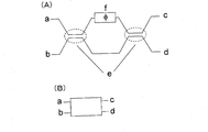
- the element switch is configured by a 2 ⁇ 2 waveguide type Mach-Zehnder interferometer as illustrated in FIG. 12 (see Non-Patent Document 1).
- FIG. 12A is a diagram illustrating a two-input (a, b), two-output (c, d) waveguide type Mach-Zehnder interferometer as an element switch, and (B) is a simplified representation of the element switch. Is shown.
- the illustrated waveguide type Mach-Zehnder interferometer is composed of two 3 dB splitters (e) and a phase shifter (f), and can change the branching ratio by the phase shift amount of the phase shifter (f).
- Output (2 ⁇ 2) variable branch The light incident from the input end a or b is divided into two light waves by the left 3dB splitter (e), propagates through the upper and lower optical paths of the same length, and then combined by the right 3dB splitter (e).
- the way of output from the terminals c and d varies depending on the phase change ⁇ given to the phase shifter (f).
- the waveguide type Mach-Zehnder interferometer is a 2 ⁇ 2 variable branch whose branching ratio can be continuously changed by the phase shifter, but the conventional waveguide type N ⁇ N matrix switch is a waveguide type Mach.
- the Zender interferometer was used only as a crossbar switch, and no other branching ratio state was used.
- the node device has both a cross-connect (switching of one-to-one connection relationship) function and a function of distributing one input signal to a plurality of output ports.
- the conventional single (1 ⁇ N) branch element has the function of distributing one input signal to a plurality of output ports, but the number of branches and the output port of the branch destination Is fixed, and the output port of the branched signal cannot be set arbitrarily, so that it cannot cope with services such as video distribution.
- the present invention solves such problems, and in a waveguide type optical switch (matrix switch) with N inputs and N outputs (N ⁇ N), a cross-connect (switching of one-to-one connection relationship) function and one input It is intended to provide a function for distributing signals to a plurality of output ports.
- Another object of the present invention is to create all possible one-to-one connections, distribution, and a mixed state of both by appropriately determining the role of the variable branch of each of the N 2 element switches.
- N 2 element switches having 2 inputs and 2 outputs are arranged on a lattice of a matrix of N rows and N columns, where N is an integer.
- Each of the N 2 element switches has a variable branch configuration in which the branch ratio of the two outputs is made variable, and the N 2 element switches include the element switch and the bar state set to the cross state.
- the element switch set to 1 the element switch set to be distributed to two outputs at a predetermined branching ratio is included.
- This element switch is a two-input two-output waveguide type Mach-Zehnder interferometer which is composed of two 3 dB ⁇ splitters and a phase shifter and whose branching ratio can be changed by the phase shift amount of the phase shifter.
- a single waveguide type optical switch can be used as an N ⁇ N cross-connect or a 1 ⁇ M branch (M ⁇ N) (M and N are integers), as well as a cross-connect function and a branch function. Mixing operation is possible. Further, in the 1 ⁇ M branch, the number of branches and the branch destination output port can be arbitrarily set.
- each of the element switches constituting a general N ⁇ N waveguide type optical switch a cross state, a bar state, a branch of a predetermined distribution ratio, and respective arrangements are appropriately selected. By correcting, it is possible to create a desired one-to-one connection, distribution to multiple ports, or a mixture of both.
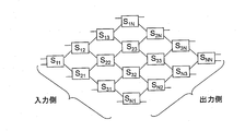
- FIG. 1 It is a figure which illustrates the waveguide type optical switch (matrix switch) structure comprised based on this invention.
- A) is a figure explaining operation
- (B) is a figure which shows a cross connection and (C) respectively shows a bar connection. It is a figure explaining the setting of each variable branch in the case of performing 1 ⁇ 4 distribution of one system ( ⁇ ).
- ⁇ 1x3 distribution of 1 system ((circle)) and 1x1 connection of 1 system ((circle)) are performed.
- 1x2 distribution of 2 systems ((circle) and ⁇ ) is performed.
- FIG. 1 It is a figure which illustrates the case where 1x2 distribution of 1 system ((circle)) and 1x1 connection of 2 systems ( ⁇ , ⁇ ) are performed. It is a figure which illustrates another waveguide type optical switch (matrix switch) structure different from FIG. 1 comprised based on this invention. It is a figure explaining the setting of each variable branch in the case of performing 1 ⁇ 4 distribution of one system ( ⁇ ). It is a figure which illustrates the case where 1x3 distribution of 1 system ((circle)) and 1x1 connection of 1 system ((circle)) are performed. It is a figure which illustrates the case where 1x2 distribution of 2 systems ((circle) and ⁇ ) is performed.
- FIG. 1 is a diagram illustrating a two-input (a, b), two-output (c, d) waveguide type Mach-Zehnder interferometer as an element switch, and (B) shows a simplified display of the element switch.
- a matrix switch called a Pyros type uses N 2 switch cells each having 2 inputs and 2 outputs in order to eliminate variations in loss due to the number of passing switch cells (element switches). They are arranged on a matrix of rows and N columns, and are configured by appropriately connecting the input and output of the switch cell so as not to cause loss path dependency.
- FIG. 1 is a diagram illustrating a waveguide type optical switch (matrix switch) configuration configured according to the present invention.
- the illustrated waveguide type optical switch is configured by arranging N 2 element switches (S 11 to S NN ) each having 2 inputs and 2 outputs on a matrix grid of N rows and N columns.
- Each element switch is a variable input with 2 inputs and 2 outputs (2 x 2), and each element switch can be operated in either a cross state, a bar state, or a predetermined branch ratio. It is possible to have a distribution function of branching a signal and outputting it to a plurality of ports.
- FIG. 2A is a diagram for explaining the operation of the element switch shown in FIG. 1, where FIG. 2B shows a cross connection and FIG. 2C shows a bar connection.
- the element switch is configured by a 2 ⁇ 2 waveguide type Mach-Zehnder interferometer as illustrated in FIG.
- the illustrated element switch can be operated as a cross connection or a bar connection by changing the phase shift amount ⁇ of the phase shifter, in addition to a predetermined branch ratio (for example, 1: 1, 1: 2 or 1: 3).
- phase shift amount ⁇ of the phase shifter can be changed by, for example, a thermo-optic effect, a carrier plasma effect, an electro-optic effect, or the like.
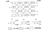
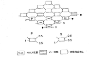
- FIG. 3 shows a variable branch setting for equally distributing one input signal to all four output ports. It is assumed that a signal is input from only one port and no signal is input to the remaining three ports.
- variable branches indicated as P, Q, and R in the figure are set so as to have the branching ratio shown in the lower part of the figure. As a result, one input signal is equally distributed to all four output ports.
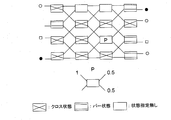
- FIG. 4 is a diagram illustrating a case where 1 ⁇ 3 distribution of 1 system ( ⁇ ) and 1 ⁇ 1 connection of 1 system ( ⁇ ) are performed. This is a case where a signal input to one port is equally distributed to three output ports, and an input to another port is connected to the remaining one output port.
- the variable branches marked P and Q in the figure are set so as to have the branching ratio shown in the lower part of the figure.
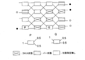
- FIG. 5 is a diagram illustrating a case where 1 ⁇ 2 distribution of two systems ( ⁇ , ⁇ ) is performed. A case where signals input to two ports are equally distributed to two output ports is shown. The variable branches marked P and Q in the figure are set so as to have the branching ratio shown in the lower part of the figure.
- FIG. 6 is a diagram illustrating a case where 1 ⁇ 2 distribution of 1 system ( ⁇ ) and 1 ⁇ 1 connection of 2 systems ( ⁇ , ⁇ ) are performed.
- a case is shown in which a signal input to one port is equally distributed to two output ports, and signals input to the two ports are connected to different output ports, respectively.
- the variable branch marked P in the figure is set so as to have the branching ratio shown in the lower part of the figure.
- FIG. 7 shows another standard matrix topology that is not Pyros but is different from FIG.
- the standard matrix topology itself shown in the figure has N 2 element switches (S 11 to S NN ) each having 2 inputs and 2 outputs arranged on a matrix grid of N rows and N columns. ,Constitute. Connection paths from the input side are element switches S 11 to S N1 , and connection paths to the output side are element switches S N1 to S NN .
- An arbitrary input side connection path has a cross point at one position between the arbitrary input side connection path and a path is set between both connection paths. For this path setting, the cross point element switch is switched from cross connection to bar connection.
- the present invention can be applied to a standard matrix topology known per se, which is conventionally configured by setting element switches to either a cross connection or a bar connection.
- all N 2 element switches (S 11 to S NN ) have two inputs and two outputs (2 ⁇ ) as described with reference to FIG. 2)
- the variable branch element switch is used.
- one or more element switches are operated at a predetermined branching ratio.
- FIGS. 8 to 11 show that the operation corresponding to FIGS. 3 to 6 is possible even with this standard matrix topology.
- FIG. 8 is a diagram for explaining the setting of each variable branch when 1 ⁇ 4 distribution of one system ( ⁇ ) is performed. This corresponds to the case of FIG.
- FIG. 9 is a diagram illustrating a case where 1 ⁇ 3 distribution of 1 system ( ⁇ ) and 1 ⁇ 1 connection of 1 system ( ⁇ ) are performed. This corresponds to the case of FIG.
- FIG. 10 is a diagram illustrating a case where 1 ⁇ 2 distribution of two systems ( ⁇ , ⁇ ) is performed. This corresponds to the case of FIG.
- FIG. 11 is a diagram illustrating a case where 1 ⁇ 2 distribution of 1 system ( ⁇ ) and 1 ⁇ 1 connection of 2 systems ( ⁇ , ⁇ ) are performed. This corresponds to the case of FIG.
- FIGS. 3 and 8 show 1 ⁇ 4 as 1 system
- FIGS. 4 and 9 show 1 ⁇ 3 and 1 ⁇ 1 as 1 system
- FIGS. 5 and 10 show 1 ⁇ 2 as 2 systems
- 6 and 11 show an example in which 1 ⁇ 2 includes 1 system and 1 ⁇ 1 includes 2 systems.
- Bars special branching ratios such as P, Q, and R above, creating the desired one-to-one connection, distribution to multiple ports, or a mixture of both by properly re-selecting each placement Can do.
- N ⁇ N matrix all possible one-to-one connections, distribution, and a mixture of both can be achieved by appropriately determining the role of the variable branch of each of the N 2 element switches. You can create a state.
Landscapes
- Engineering & Computer Science (AREA)
- Computer Networks & Wireless Communication (AREA)
- Optical Modulation, Optical Deflection, Nonlinear Optics, Optical Demodulation, Optical Logic Elements (AREA)
- Optical Integrated Circuits (AREA)
Abstract
N入力N出力(N×N)の導波路型光スイッチ(マトリックススイッチ)において、クロスコネクト(1対1の接続関係の切り替え)機能と一つの入力信号を複数の出力ポートに分配する機能を併せ持ち提供する。本発明は、N行N列のマトリックスの格子上に2入力2出力のN2個の要素スイッチを配置する。このN2個の要素スイッチはそれぞれ、2つの出力の分岐比を可変にして出力する可変分岐構成を有し、かつ、このN2個の要素スイッチは、クロス状態に設定した要素スイッチ及びバー状態に設定した要素スイッチだけでなく、所定の分岐比で2出力に分配動作させる設定にした要素スイッチを包含する。
Description
本発明は、1対1の接続関係の切り替えを行うクロスコネクト機能だけでなく、入力信号を分岐して複数のポートに出力する分配機能を持たせることができる導波路型光スイッチに関する。
N本の入線とN本の出線の間の1対1の接続関係を切り替える機能を担うノード装置は、光クロスコネクトと呼ばれ、光パスネットワークに幅広い構成可変性を持たせるために必要である。N入力N出力(N×N)の光クロスコネクトには、メムス(Micro Electro Mechanical Systems;MEMS)素子を用いるもの(特許文献1参照)、導波路型光スイッチ(マトリックススイッチ)(特許文献2参照)によるもの等がある。導波路型光スイッチは、スイッチ素子と、スイッチ素子に接続される入力及び出力のためのファイバアレイとを備えている。また、光スイッチを半導体技術で小さくしたメムス素子は、小さなミラーを半導体製造技術で基板上に作製し、静電気によりこのミラーを立ち上げて、光路を切り換えるというものである。
従来の導波路型N×Nマトリックススイッチは、N2個の2×2クロスバースイッチを要素スイッチとして用いる。要素スイッチは、図12に例示するような2×2導波路型マッハツェンダー干渉計によって構成される(非特許文献1参照)。図12(A)は、要素スイッチとしての2入力(a,b)2出力(c,d)の導波路型マッハツェンダー干渉計を例示する図であり、(B)はその要素スイッチの簡略表示を示している。図示の導波路型マッハツェンダー干渉計は、2つの3dB スプリッタ(e)と移相器(f)から構成されて、分岐比を移相器(f)の位相シフト量で変えられる、2入力2出力(2×2)の可変分岐である。入力端aまたはbから入射した光は、左側の3dB スプリッタ(e)で2つの光波に分けられ、長さの等しい上下の光路をそれぞれ伝播した後、右側の3dB スプリッタ(e)で合波される。端子c、dからの出力のされ方は、移相器(f)に与える位相変化Φによって変化する。
単位強度の光を、ポートaから入力したとき、移相器(f)に与える位相変化Φが0ラジアンであれば、ポートdへ出力される。Φがπラジアンのとき、ポートcへ出力される。ポートbから入力する場合も同様に、Φが0ラジアンのとき出力はポートc、πラジアンのとき出力はポートdに生じる。入出力の結果的な接続関係を見て、aがdに、bがcにつながっている状態をクロス状態、aがcに、bがdにつながっている状態をバー状態と呼び、2×2スイッチが取るべき2つの状態である。このように、適切な位相変化(Φ=0又はπラジアン)を与えてクロス、バーのいずれかの状態をとらせることによって、2×2スイッチとして機能する。
このように、導波路型マッハツェンダー干渉計は、移相器によって分岐比を連続的に変えられる2×2可変分岐ではあるが、従来の導波路型N×Nマトリックススイッチは、導波路型マッハツェンダー干渉計をクロスバースイッチとしてのみ利用し、それ以外の分岐比の状態が利用されることはなかった。
また、ノード装置は、クロスコネクト(1対1の接続関係の切り替え)機能と一つの入力信号を複数の出力ポートに分配する機能を併せ持つことが、今後の、例えば映像配信等のサービスにとって、望まれる。しかし、従来型の単体の(1×N)分岐素子(特許文献3参照)では、一つの入力信号を複数の出力ポートに分配する機能を有しているものの、分岐数や分岐先の出力ポートは固定であり、分岐した信号の出力ポートを任意に設定できることができないために、映像配信等のサービスに対応することができない。
R. Nagase, A. Himeno, M. Okuno, K. Kato, K. Yukimasa, M. Kawachi, "Silica-Based 8×8 Optical Matrix Switch Module with Hybrid Integrated Driving Circuits and its System Application", Journal of Lightwave Technology, Vol.12, no.9, 1631 (1994).
本発明は、係る問題点を解決して、N入力N出力(N×N)の導波路型光スイッチ(マトリックススイッチ)において、クロスコネクト(1対1の接続関係の切り替え)機能と一つの入力信号を複数の出力ポートに分配する機能を併せ持ち提供することを目的としている。
また、本発明は、N2個の要素スイッチそれぞれの可変分岐の役割を適切に決めることによって、起こり得る全ての、1対1接続、分配、両者の混合状態をつくることを目的としている。
本発明の導波路型光スイッチは、Nを整数として、N行N列のマトリックスの格子上に2入力2出力のN2個の要素スイッチを配置する。このN2個の要素スイッチはそれぞれ、2つの出力の分岐比を可変にして出力する可変分岐構成を有し、かつ、このN2個の要素スイッチは、クロス状態に設定した要素スイッチ及びバー状態に設定した要素スイッチだけでなく、所定の分岐比で2出力に分配動作させる設定にした要素スイッチを包含する。
要素スイッチの入力及び出力を所定の関係で接続して構成したことにより、クロスコネクト機能だけでなく、入力信号を分岐して複数のポートに出力する分配機能を持たせることができる。この要素スイッチは、2つの3dB スプリッタと移相器から構成されて、分岐比を移相器の位相シフト量で変えられる2入力2出力の導波路型マッハツェンダー干渉計である。
本発明によれば、ひとつの導波路型光スイッチで、N×Nクロスコネクトとしても1×M分岐(M≦N)(M、Nは整数)としても使えるほか、クロスコネクト機能と分岐機能の混合動作が可能となる。さらに、1×M分岐においては、分岐数や分岐先の出力ポートを任意に設定することができる。
また、本発明によれば、一般的なN×Nの導波路型光スイッチを構成する要素スイッチのそれぞれとして、クロス状態、バー状態、所定の分配比率の分岐、及びそれぞれの配置を適切に選び直すことによって、所望の、1対1接続や複数ポートへの分配、または両者の混合状態をつくることができる。
以下、本発明をパイロス(PILOSS:Path-independent Insertion Loss)として知られるトポロジーのマトリックススイッチに適用した場合を例として説明する。パイロス型と称されるマトリックススイッチ(特許文献2参照)は、通過するスイッチセル(要素スイッチ)の数による損失のバラツキを解消するために、各々2入力2出力のN2個のスイッチセルをN行N列のマトリックスの格子上に配置し、損失のパス依存性が生じないようにスイッチセルの入力及び出力を適切に接続して構成される。
図1は、本発明に基づき構成した導波路型光スイッチ(マトリックススイッチ)構成を例示する図である。図示の導波路型光スイッチは、各々2入力2出力のN2個の要素スイッチ(S11~SNN)をN行N列のマトリックスの格子上に配置して、構成する。各要素スイッチは、2入力2出力(2×2)の可変分岐であり、それぞれ、クロス状態、バー状態、或いは所定の分岐比のいずれかで動作させることにより、クロスコネクト機能だけでなく、入力信号を分岐して複数のポートに出力する分配機能を持たせることが可能になる。
図2(A)は、図1に示す要素スイッチの動作を説明する図であり、(B)はクロス接続を、また、(C)はバー接続をそれぞれ示している。要素スイッチは、図12に例示したような2×2導波路型マッハツェンダー干渉計により構成される。例示の要素スイッチは、上述したように、移相器(f)の位相シフト量Φ=0の場合、図2(B)に示すクロス接続を与える状態になり、Φ=πの場合、(C)に示すバー接続を与える状態になる。図示の要素スイッチは、移相器の位相シフト量Φを変えることにより、クロス接続、或いはバー接続として動作させる以外にも、2つの出力ポートに所定の分岐比(例えば、1:1、1:2、或いは1:3等)で出力させる。
図2(A)に示すように、要素スイッチの入力ポートbから光電力1.0の信号を入力したとき、出力ポートc、dにそれぞれ、cos2(Φ/2)、sin2(Φ/2)の光電力で分配される。或いは、入力ポートaから入力した場合は、出力ポートc、dにそれぞれ、sin2(Φ/2)、cos2(Φ/2)の光電力で分配される。移相器の位相シフト量Φは、公知のように、例えば、熱光学効果、キャリアプラズマ効果、電気光学効果等によって変化させることができる。
次に、図3~図6を参照して、本発明の導波路型光スイッチの動作例について説明する。図3は、1系統(〇)の1×4分配を行う場合の、各可変分岐の設定を説明する図である。4×4のマトリックススイッチ(ポート数N= 4)の場合を例にとる。クロス状態、バー状態のほか、要素スイッチP、Q、Rについては図下に示す、特別な分岐を持たせる。指定のない可変分岐(図中に空白で示した要素スイッチ)の状態は何であってもよい。図3は、一つの入力信号を4つ全ての出力ポートに等分配するための可変分岐の設定を示している。信号を入力するのは1つのポートだけからとし、残りの3ポートへの信号入力は無いものとする。クロスまたはバー状態にする分岐のほかに、図中P,Q、Rと記した可変分岐は、図下に示した分岐比を持つように設定する。これによって、一つの入力信号が、4つ全ての出力ポートに、等分配される。
図4は、1系統(〇)の1×3分配と1系統(●)の1×1接続を行う場合を例示する図である。ある一つのポートに入力される信号を3つの出力ポートに等分配し、別のひとつのポートへの入力を、残る1つの出力ポートに接続する場合である。図中P,Qと記した可変分岐は、図下に示した分岐比を持つように設定する。
図5は、2系統(〇、●)の1×2分配を行う場合を例示する図である。2つのポートに入力される信号を、それぞれ2つの出力ポートに等分配する場合を示す。図中P,Qと記した可変分岐は、図下に示した分岐比を持つように設定する。
図6は、1系統(〇)の1×2分配と2系統(□、●)の1×1接続を行う場合を例示する図である。1つのポートに入力される信号を2つの出力ポートに等分配し、2つのポートに入力される信号をそれぞれ、異なる出力ポートに接続する場合を示す。図中Pと記した可変分岐は、図下に示した分岐比を持つように設定する。
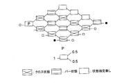
図7に、パイロスではないが、図1とは異なるもう1つの標準的なマトリックストポロジーを示す。図示のような標準的なマトリックストポロジー自体は、公知のように、各々2入力2出力のN2個の要素スイッチ(S11~SNN)をN行N列のマトリックスの格子上に配置して、構成する。入力側からの接続路は要素スイッチS11~SN1となり、出力側への接続路は要素スイッチSN1~SNNとなる。任意の入力側接続路は、任意の出力側接続路との間の1箇所でクロスポイントを持つことにより、両接続路の間にパスが設定される。このパス設定のために、クロスポイントの要素スイッチは、クロス接続からバー接続に切り換えられる。このように、従来、要素スイッチをクロス接続か、バー接続かのいずれかに設定して構成されていたそれ自体は公知の標準的なマトリックストポロジーにも、本発明を適用することができる。
本発明を、標準的なマトリックストポロジーに適用するに際して、N2個の要素スイッチ(S11~SNN)の全てに対して、図2を参照して説明したような2入力2出力(2×2)の可変分岐の要素スイッチを用いる。そして、このN2個の要素スイッチのいくつかを、クロス状態、或いはバー状態に設定するだけでなく、1つ或いは複数の要素スイッチを所定の分岐比で動作させる。
図8~図11は、この標準的なマトリックストポロジーでも、先の図3~図6に対応した動作が可能であることを示している。
図8は、1系統(〇)の1×4分配を行う場合の、各可変分岐の設定を説明する図である。図3の場合に対応する。
図9は、1系統(〇)の1×3分配と1系統(●)の1×1接続を行う場合を例示する図である。図4の場合に対応する。
図10は、2系統(〇、●)の1×2分配を行う場合を例示する図である。図5の場合に対応する。
図11は、1系統(〇)の1×2分配と2系統(□、●)の1×1接続を行う場合を例示する図である。図6の場合に対応する。
上述のように、図3と図8は1×4を1系統、図4と図9は1×3と1×1をそれぞれ1系統づつ、図5と図10は1×2を2系統、図6と図11は1×2を1系統、1×1を2系統、含む場合の1例であるが、信号の入力先と出力先として、例示したものと異なるポートを選ぶ場合でも、クロス、バー、上記のP、Q、Rのような特別な分岐比、それぞれの配置を適切に選び直すことによって所望の、1対1接続や複数ポートへの分配、または両者の混合状態をつくることができる。更には、一般的なN×Nのマトリックスの場合についても、N2個の要素スイッチそれぞれの可変分岐の役割を適切に決めることによって、起こり得る全ての、1対1接続、分配、両者の混合状態をつくることができる。
以上、本開示にて幾つかの実施の形態を単に例示として詳細に説明したが、本発明の新規な教示及び有利な効果から実質的に逸脱せずに、その実施の形態には多くの改変例が可能である。
Claims (3)
- Nを整数として、N行N列のマトリックスの格子上に2入力2出力のN2個の要素スイッチを配置した導波路型光スイッチにおいて、
前記N2個の要素スイッチはそれぞれ、2つの出力の分岐比を可変にして出力する可変分岐構成を有し、かつ
前記N2個の要素スイッチは、クロス状態に設定した要素スイッチ及びバー状態に設定した要素スイッチだけでなく、所定の分岐比で2出力に分配動作させる設定にした要素スイッチを包含することを特徴とする導波路型光スイッチ。 - 前記要素スイッチの入力及び出力を所定の関係で接続して構成したことにより、クロスコネクト機能だけでなく、入力信号を分岐して複数のポートに出力する分配機能を持たせた請求項1に記載の導波路型光スイッチ。
- 前記要素スイッチは、2つの3dB スプリッタと移相器から構成されて、分岐比を移相器の位相シフト量で変えられる2入力2出力の導波路型マッハツェンダー干渉計である請求項1に記載の導波路型光スイッチ。
Applications Claiming Priority (2)
| Application Number | Priority Date | Filing Date | Title |
|---|---|---|---|
| JP2011-085323 | 2011-04-07 | ||
| JP2011085323A JP2012220664A (ja) | 2011-04-07 | 2011-04-07 | 導波路型光スイッチ |
Publications (1)
| Publication Number | Publication Date |
|---|---|
| WO2012137555A1 true WO2012137555A1 (ja) | 2012-10-11 |
Family
ID=46968959
Family Applications (1)
| Application Number | Title | Priority Date | Filing Date |
|---|---|---|---|
| PCT/JP2012/054373 WO2012137555A1 (ja) | 2011-04-07 | 2012-02-23 | 導波路型光スイッチ |
Country Status (2)
| Country | Link |
|---|---|
| JP (1) | JP2012220664A (ja) |
| WO (1) | WO2012137555A1 (ja) |
Cited By (1)
| Publication number | Priority date | Publication date | Assignee | Title |
|---|---|---|---|---|
| JP2014086802A (ja) * | 2012-10-22 | 2014-05-12 | Oki Electric Ind Co Ltd | 多端末量子鍵配送システム |
Families Citing this family (2)
| Publication number | Priority date | Publication date | Assignee | Title |
|---|---|---|---|---|
| CN103973369B (zh) * | 2014-05-16 | 2016-03-23 | 电子科技大学 | 一种光开关矩阵的状态配置方法 |
| JP6950593B2 (ja) * | 2018-03-09 | 2021-10-13 | 日本電信電話株式会社 | 光入出力装置およびその作製方法 |
Citations (2)
| Publication number | Priority date | Publication date | Assignee | Title |
|---|---|---|---|---|
| JP2003005231A (ja) * | 2001-06-26 | 2003-01-08 | Nippon Telegr & Teleph Corp <Ntt> | 光マトリクススイッチ |
| WO2011043122A1 (ja) * | 2009-10-07 | 2011-04-14 | 日本電気株式会社 | 光信号送信装置、光信号受信装置、波長多重分離光通信装置および波長パスシステム |
-
2011
- 2011-04-07 JP JP2011085323A patent/JP2012220664A/ja active Pending
-
2012
- 2012-02-23 WO PCT/JP2012/054373 patent/WO2012137555A1/ja active Application Filing
Patent Citations (2)
| Publication number | Priority date | Publication date | Assignee | Title |
|---|---|---|---|---|
| JP2003005231A (ja) * | 2001-06-26 | 2003-01-08 | Nippon Telegr & Teleph Corp <Ntt> | 光マトリクススイッチ |
| WO2011043122A1 (ja) * | 2009-10-07 | 2011-04-14 | 日本電気株式会社 | 光信号送信装置、光信号受信装置、波長多重分離光通信装置および波長パスシステム |
Non-Patent Citations (1)
| Title |
|---|
| MIZUTANI, K. ET AL.: "Demonstraion of Multi- Degree Color/Direction-Independent Waveguide- Based Transponder-Aggregator for Flexible Optical Path Networks", ECOC 2010, September 2010 (2010-09-01), pages 1 - 3, XP031789618 * |
Cited By (1)
| Publication number | Priority date | Publication date | Assignee | Title |
|---|---|---|---|---|
| JP2014086802A (ja) * | 2012-10-22 | 2014-05-12 | Oki Electric Ind Co Ltd | 多端末量子鍵配送システム |
Also Published As
| Publication number | Publication date |
|---|---|
| JP2012220664A (ja) | 2012-11-12 |
Similar Documents
| Publication | Publication Date | Title |
|---|---|---|
| Tanizawa et al. | Ultra-compact 32× 32 strictly-non-blocking Si-wire optical switch with fan-out LGA interposer | |
| Dupuis et al. | Design and Fabrication of Low-Insertion-Loss and Low-Crosstalk Broadband $2\times 2$ Mach–Zehnder Silicon Photonic Switches | |
| Dupuis et al. | Modeling and Characterization of a Nonblocking $4\times 4$ Mach–Zehnder Silicon Photonic Switch Fabric | |
| JP3842511B2 (ja) | 多重ポート・カプラを使用する光学的空間スイッチ | |
| US9794656B2 (en) | Modular photonic switch architecture | |
| JP5913139B2 (ja) | 導波路型光スイッチ | |
| US6292597B1 (en) | N×N non-blocking optical switch | |
| JP5222083B2 (ja) | 多方路光スイッチ | |
| CN106990481B (zh) | 2×2多模光开关及片上网络 | |
| JP6533743B2 (ja) | 光クロスコネクト装置 | |
| WO2012137555A1 (ja) | 導波路型光スイッチ | |
| US9784921B1 (en) | Switch matrix incorporating polarization controller | |
| CA2258333A1 (en) | An n x n non-blocking optical switch | |
| Suzuki et al. | High-Speed Optical 1$\times $4 Switch Based on Generalized Mach–Zehnder Interferometer With Hybrid Configuration of Silica-Based PLC and Lithium Niobate Phase-Shifter Array | |
| JP2006292872A (ja) | マトリクス光スイッチ | |
| Wu et al. | Large-port-count MEMS silicon photonics switches | |
| JP6420715B2 (ja) | 光信号処理装置 | |
| Bahadori et al. | Loss and crosstalk of scalable MZI-based switch topologies in silicon photonic platform | |
| JP2004233619A (ja) | 光スイッチ及び光波長ルータ | |
| Kawashima et al. | Multi-port optical switch based on silicon photonics | |
| US11405702B2 (en) | Optical signal processing device and method for controlling same | |
| JP7189473B2 (ja) | 光信号処理装置 | |
| Hoppe et al. | Improved Optical 1xN On-Chip-Switches Based on Generalized Mach-Zehnder Interferometers | |
| JP2004077854A (ja) | 光スイッチ及びその使用方法 | |
| Hunter | Planar optical space switch architectures |
Legal Events
| Date | Code | Title | Description |
|---|---|---|---|
| 121 | Ep: the epo has been informed by wipo that ep was designated in this application |
Ref document number: 12767811 Country of ref document: EP Kind code of ref document: A1 |
|
| NENP | Non-entry into the national phase |
Ref country code: DE |
|
| 122 | Ep: pct application non-entry in european phase |
Ref document number: 12767811 Country of ref document: EP Kind code of ref document: A1 |