WO2020004273A1 - 導電性粒子、導電材料及び接続構造体 - Google Patents
導電性粒子、導電材料及び接続構造体 Download PDFInfo
- Publication number
- WO2020004273A1 WO2020004273A1 PCT/JP2019/024743 JP2019024743W WO2020004273A1 WO 2020004273 A1 WO2020004273 A1 WO 2020004273A1 JP 2019024743 W JP2019024743 W JP 2019024743W WO 2020004273 A1 WO2020004273 A1 WO 2020004273A1
- Authority
- WO
- WIPO (PCT)
- Prior art keywords
- conductive
- particles
- conductive particles
- soft magnetic
- insulating
- Prior art date
- Legal status (The legal status is an assumption and is not a legal conclusion. Google has not performed a legal analysis and makes no representation as to the accuracy of the status listed.)
- Ceased
Links
Images

Classifications
-
- B—PERFORMING OPERATIONS; TRANSPORTING
- B32—LAYERED PRODUCTS
- B32B—LAYERED PRODUCTS, i.e. PRODUCTS BUILT-UP OF STRATA OF FLAT OR NON-FLAT, e.g. CELLULAR OR HONEYCOMB, FORM
- B32B7/00—Layered products characterised by the relation between layers; Layered products characterised by the relative orientation of features between layers, or by the relative values of a measurable parameter between layers, i.e. products comprising layers having different physical, chemical or physicochemical properties; Layered products characterised by the interconnection of layers
- B32B7/02—Physical, chemical or physicochemical properties
- B32B7/025—Electric or magnetic properties
-
- H—ELECTRICITY
- H01—ELECTRIC ELEMENTS
- H01B—CABLES; CONDUCTORS; INSULATORS; SELECTION OF MATERIALS FOR THEIR CONDUCTIVE, INSULATING OR DIELECTRIC PROPERTIES
- H01B1/00—Conductors or conductive bodies characterised by the conductive materials; Selection of materials as conductors
-
- H—ELECTRICITY
- H01—ELECTRIC ELEMENTS
- H01B—CABLES; CONDUCTORS; INSULATORS; SELECTION OF MATERIALS FOR THEIR CONDUCTIVE, INSULATING OR DIELECTRIC PROPERTIES
- H01B1/00—Conductors or conductive bodies characterised by the conductive materials; Selection of materials as conductors
- H01B1/20—Conductive material dispersed in non-conductive organic material
- H01B1/22—Conductive material dispersed in non-conductive organic material the conductive material comprising metals or alloys
-
- H—ELECTRICITY
- H01—ELECTRIC ELEMENTS
- H01B—CABLES; CONDUCTORS; INSULATORS; SELECTION OF MATERIALS FOR THEIR CONDUCTIVE, INSULATING OR DIELECTRIC PROPERTIES
- H01B5/00—Non-insulated conductors or conductive bodies characterised by their form
-
- H—ELECTRICITY
- H01—ELECTRIC ELEMENTS
- H01B—CABLES; CONDUCTORS; INSULATORS; SELECTION OF MATERIALS FOR THEIR CONDUCTIVE, INSULATING OR DIELECTRIC PROPERTIES
- H01B5/00—Non-insulated conductors or conductive bodies characterised by their form
- H01B5/16—Non-insulated conductors or conductive bodies characterised by their form comprising conductive material in insulating or poorly conductive material, e.g. conductive rubber
-
- H—ELECTRICITY
- H01—ELECTRIC ELEMENTS
- H01R—ELECTRICALLY-CONDUCTIVE CONNECTIONS; STRUCTURAL ASSOCIATIONS OF A PLURALITY OF MUTUALLY-INSULATED ELECTRICAL CONNECTING ELEMENTS; COUPLING DEVICES; CURRENT COLLECTORS
- H01R11/00—Individual connecting elements providing two or more spaced connecting locations for conductive members which are, or may be, thereby interconnected, e.g. end pieces for wires or cables supported by the wire or cable and having means for facilitating electrical connection to some other wire, terminal, or conductive member, blocks of binding posts
- H01R11/01—Individual connecting elements providing two or more spaced connecting locations for conductive members which are, or may be, thereby interconnected, e.g. end pieces for wires or cables supported by the wire or cable and having means for facilitating electrical connection to some other wire, terminal, or conductive member, blocks of binding posts characterised by the form or arrangement of the conductive interconnection between the connecting locations
Definitions
- the present invention relates to a conductive particle having a conductive portion disposed on the surface of a base particle.
- the present invention also relates to a conductive material and a connection structure using the conductive particles.
- anisotropic conductive materials such as anisotropic conductive paste and anisotropic conductive film are widely known.
- anisotropic conductive material conductive particles are dispersed in a binder resin.
- conductive particles obtained by subjecting a surface of a conductive layer to insulation treatment are used as the conductive particles.
- the anisotropic conductive material is used to obtain various connection structures.
- Examples of the connection using the anisotropic conductive material include connection between a flexible printed board and a glass substrate (FOG (Film @ on @ Glass)), connection between a semiconductor chip and a flexible printed board (COF (Chip @ on @ Film)), The connection between a semiconductor chip and a glass substrate (COG (Chip @ on Glass)), the connection between a flexible printed board and a glass epoxy substrate (FOB (Film @ on @ Board)), and the like can be given.
- Patent Literature 1 discloses a conductive particle including a base particle having a plating layer, and insulating particles covering the surface of the base particle.
- the base particles are particles in which the surface of a plastic core is covered with the plating layer.
- the plating layer has at least a nickel / phosphorus alloy layer.
- the particle diameter of the base particles is 2.0 ⁇ m or more and 3.0 ⁇ m or less.
- the base particles have a saturation magnetization of 45 emu / cm 3 or less.
- the particle diameter of the insulating particles is 180 nm or more and 500 nm or less.
- Patent Document 1 the saturation magnetization of the base particles is 45 emu / cm 3 or less.
- Patent Literature 1 merely describes that the saturation magnetization is controlled to a specific range, and does not describe any residual magnetization.
- Conventional conductive particles have a conductive metal such as nickel on the surface by plating or the like, and are used for electrical connection between electrodes. Further, in the conventional conductive particles, a metal such as nickel having magnetism is magnetized in a surrounding environment or a manufacturing process, and the conductive particles may aggregate (magnetic aggregation).
- a method for solving the above-mentioned problem as described in Patent Literature 1 and the like, a method of containing phosphorus in a plating layer to reduce saturation magnetization and the like can be mentioned.
- the connection resistance between the electrodes may also increase. .
- the conventional conductive particles can reduce the saturation magnetization, it is sometimes difficult to sufficiently reduce the residual magnetization. In order to suppress the magnetic aggregation of the conductive particles, it is necessary to reduce not only the saturation magnetization but also the residual magnetization. With conventional conductive particles, it is difficult to achieve both a reduction in connection resistance between electrodes and a suppression of magnetic aggregation.
- a conductive particle comprising: a base particle; and a conductive portion disposed on a surface of the base particle, wherein a ratio of a residual magnetization to a saturation magnetization is 0.6 or less.
- the residual magnetization is 0.02 A / m or less.
- the conductive particles include a soft magnetic body disposed on an outer surface of the conductive unit.
- the conductive particles include an insulating portion disposed between the conductive portion and the soft magnetic material portion, the soft magnetic material portion, the conductive material via the insulating portion Located on the outer surface of the part.
- a distance between the conductive portion and the soft magnetic material portion is 10 nm or more and 500 nm or less.
- the conductive particles include a plurality of the soft magnetic material portions, a plurality of the soft magnetic material portions are separated, and are disposed on an outer surface of the conductive portion. ing.
- an area of a portion of the surface of the conductive portion covered by the soft magnetic material portion with respect to an entire surface area of the conductive portion is 30% or more.
- an area of a portion of the surface of the conductive portion covered by the soft magnetic material portion with respect to an entire surface area of the conductive portion is 40% or more.
- the conductive particles include a plurality of insulating particles arranged on an outer surface of the conductive portion.
- a conductive material including the above-described conductive particles and a binder resin.
- a first connection target member having a first electrode on a surface
- a second connection target member having a second electrode on a surface
- the first connection target member A connection portion connecting the second connection target member, and the material of the connection portion is the above-described conductive particles, or a conductive material including the conductive particles and a binder resin.
- a connection structure is provided in which the first electrode and the second electrode are electrically connected by the conductive portion of the conductive particles.
- the conductive particles according to the present invention include base particles and conductive portions disposed on the surface of the base particles.
- the ratio of the residual magnetization to the saturation magnetization is 0.6 or less. Since the conductive particles according to the present invention have the above-described configuration, the connection resistance between the electrodes can be effectively reduced, and the magnetic aggregation can be effectively suppressed.
- the conductive particles according to the present invention include base particles, and a conductive part disposed on the surface of the base particles.
- the ratio of the residual magnetization to the saturation magnetization is 0.6 or less.
- the conductive particles according to the present invention have the above configuration, the connection resistance between the electrodes can be effectively reduced, and the magnetic aggregation can be effectively suppressed.
- a metal such as nickel having magnetism is magnetized in the surrounding environment or a manufacturing process, and the conductive particles may aggregate (magnetic aggregation).
- a method of suppressing the aggregation (magnetic aggregation) of the conductive particles a method of reducing saturation magnetization by adding phosphorus to the plating layer can be cited.
- the resistance value of the conductive particles significantly increases, and when the electrodes are electrically connected using the conductive particles, the connection resistance between the electrodes may also increase. .
- the present inventors have found that by using specific conductive particles, it is possible to achieve both a low connection resistance between electrodes and a suppression of magnetic aggregation of the conductive particles.
- the connection resistance between the electrodes can be effectively reduced, and the magnetic aggregation of the conductive particles can be effectively suppressed.
- the ratio of the residual magnetization to the saturation magnetization is: 0.6 or less.
- the ratio (residual magnetization / saturation magnetization) is preferably 0.5 or less, more preferably 0.3 or less, and most preferably 0.0.
- the ratio (residual magnetization / saturation magnetization) is preferably as close to 0.0 as possible from the viewpoint of more effectively reducing the connection resistance between the electrodes and suppressing the magnetic aggregation more effectively.
- the ratio (residual magnetization / saturation magnetization) is equal to or less than the upper limit, the connection resistance between the electrodes can be more effectively reduced, and the magnetic aggregation can be more effectively suppressed.
- the lower limit of the ratio (remanent magnetization / saturation magnetization) is not particularly limited.
- the ratio (residual magnetization / saturation magnetization) is, for example, preferably 0.001 or more, and more preferably 0.01 or more.
- the residual magnetization of the conductive particles is preferably 0.02 A / m (20 emu / cm 3 ) or less.
- the residual magnetization is preferably 0.015A / m (15emu / cm 3 ) or less, more preferably 0.01A / m (10emu / cm 3 ) or less, more preferably 0.005A / m (5emu / cm 3 ) Or less, most preferably 0.0000 A / m (0.0 emu / cm 3 ).
- the above-mentioned residual magnetization is preferably as close to 0.0000 A / m (0.0 emu / cm 3 ) as possible.
- the residual magnetization is equal to or less than the upper limit, the connection resistance between the electrodes can be more effectively reduced, and the magnetic aggregation can be more effectively suppressed.
- the lower limit of the residual magnetization of the conductive particles is not particularly limited.
- the residual magnetization is preferably, for example, not less than 0.0001 A / m (0.1 emu / cm 3 ).
- the residual magnetization of the conductive particles can be controlled, for example, by adjusting the coverage by a soft magnetic material portion described later.
- the remanence can be reduced by increasing the coverage by the soft magnetic material portion, and the remnant magnetization can be increased by reducing the coverage by the soft magnetic material portion.
- the saturation magnetization of the conductive particles is preferably 0.2 A / m (200 emu / cm 3 ) or less.
- the saturation magnetization is preferably 0.1 A / m (100 emu / cm 3 ) or less, more preferably 0.08 A / m (80 emu / cm 3 ) or less, and even more preferably 0.05 A / m (50 emu / cm 3 ). It is as follows. When the saturation magnetization is equal to or less than the upper limit, magnetic aggregation can be more effectively suppressed.
- the saturation magnetization of the conductive particles is preferably 0.001 A / m (1 emu / cm 3 ) or more.
- the saturation magnetization is preferably 0.005A / m (5emu / cm 3 ) or more, more preferably 0.01A / m (10emu / cm 3 ) or more, more preferably 0.015A / m (15emu / cm 3 ) That is all.
- the saturation magnetization is at least the lower limit, the conductive particles in the anisotropic conductive material can be efficiently arranged by the external magnetic field.
- the saturation magnetization of the conductive particles can be controlled, for example, by adjusting the thickness of the conductive layer or the conductive portion.
- the saturation magnetization can be increased by increasing the thickness of the conductive layer or the conductive portion, and the saturation magnetization can be reduced by decreasing the thickness of the conductive layer or the conductive portion.
- the residual magnetization and saturation magnetization of the conductive particles can be measured using a vibrating sample magnetometer (“PV-300-5” manufactured by Toei Kagaku Sangyo Co., Ltd.). Specifically, it can be measured as follows.
- ⁇ ⁇ ⁇ ⁇ Calibrate the vibrating sample magnetometer using the nickel powder encapsulated capsule as a calibration sample for the device.
- the conductive particles are weighed into a capsule and attached to a sample holder.
- the sample holder is set on the magnetometer main body, and a magnetization curve is obtained by measurement at a temperature of 20 ° C. (constant temperature), a maximum applied magnetic field of 20 kOe, and a speed of 3 minutes / loop.
- the residual magnetization and the saturation magnetization (A / m) are determined from the obtained magnetization curve.
- the particle diameter of the conductive particles is preferably 0.5 ⁇ m or more, more preferably 1 ⁇ m or more, preferably 100 ⁇ m or less, more preferably 60 ⁇ m or less, even more preferably 30 ⁇ m or less, further preferably 10 ⁇ m or less, particularly preferably. Is 5 ⁇ m or less.
- the particle size of the conductive particles is equal to or greater than the lower limit and equal to or less than the upper limit, when connecting the electrodes using the conductive particles, the contact area between the conductive particles and the electrodes is sufficiently large, In addition, aggregated conductive particles are less likely to be formed when forming the conductive portion. Further, the distance between the electrodes connected via the conductive particles does not become too large, and the conductive portion does not easily peel off from the surface of the base particles.
- the particle diameter of the conductive particles is preferably an average particle diameter, and more preferably a number average particle diameter.
- the particle size of the conductive particles is, for example, by observing 50 arbitrary conductive particles with an electron microscope or an optical microscope, calculating the average value of the particle size of each conductive particle, or performing laser diffraction type particle size distribution measurement. Or by going.
- the particle diameter of one conductive particle is determined as a particle diameter in a circle equivalent diameter.
- the average particle diameter of any 50 conductive particles in the equivalent circle diameter is substantially equal to the average particle diameter in the equivalent sphere diameter.
- the particle diameter of one conductive particle is obtained as a particle diameter in a sphere equivalent diameter.
- the particle size of the conductive particles is preferably calculated by a laser diffraction type particle size distribution measurement.
- the coefficient of variation (CV value) of the particle size of the conductive particles is preferably 10% or less, more preferably 5% or less.
- the variation coefficient of the particle diameter of the conductive particles is equal to or less than the upper limit, the reliability of conduction between the electrodes and the reliability of insulation can be more effectively improved.
- the coefficient of variation (CV value) can be measured as follows.
- the shape of the conductive particles is not particularly limited.
- the shape of the conductive particles may be spherical or may be other than spherical, such as flat.
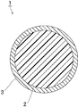
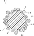
- FIG. 1 is a cross-sectional view showing the conductive particles according to the first embodiment of the present invention.
- the conductive particles 1 shown in FIG. 1 include the base particles 2 and the conductive portions 3.
- the conductive part 3 is a conductive layer.
- the conductive portion 3 covers the surface of the base particles 2.
- the conductive particles 1 are coated particles in which the surfaces of the base particles 2 are coated with the conductive portions 3.
- the conductive particles 1 have a conductive portion 3 on the surface.
- the conductive part 3 is a single-layer conductive part (conductive layer).
- the conductive portion may cover the entire surface of the base particle, or the conductive portion may cover a part of the surface of the base particle.
- the conductive portion may be a single-layer conductive portion or a multilayer conductive portion including two or more layers.
- the conductive particles 1 have no core material unlike the conductive particles 51 described below.
- the conductive particles 1 do not have protrusions on the conductive surface, and do not have protrusions on the outer surface of the conductive portion 3.
- the conductive particles 1 are spherical. However, the conductive particles 1 may have a core substance, may have protrusions on the conductive surface, or may have protrusions on the outer surface of the conductive portion 3.
- the conductive particles need not have protrusions on the conductive surface, may not have protrusions on the outer surface of the conductive portion, and may be spherical.
- the conductive particles 1 have no insulating particles, unlike the conductive particles 11, 21, 41, and 51 described below. However, the conductive particles 1 may have insulating particles arranged on the outer surface of the conductive portion 3.
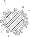
- FIG. 2 is a cross-sectional view showing the conductive particles according to the second embodiment of the present invention.
- the conductive particles 11 are different from the conductive particles 1 and have a soft magnetic material portion 12 and insulating particles 13.
- the conductive particles 11 include the insulating particles 13 that are not in contact with the soft magnetic body 12.
- the conductive particles may have a soft magnetic part or may not have a soft magnetic part.
- the conductive particles may have insulating particles or may not have insulating particles.
- the soft magnetic part is disposed on an outer surface of the conductive part. It is preferable that the soft magnetic part is not in contact with the conductive part.
- the insulating particles are preferably arranged on an outer surface of the conductive part.
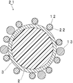
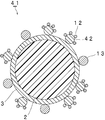
- FIG. 3 is a cross-sectional view showing the conductive particles according to the third embodiment of the present invention.
- the insulating portion 42 is a material having an insulating property.
- the insulating part 42 is an insulating particle.
- the insulating part 42 is disposed on the outer surface of the conductive part 3, and the soft magnetic body part 12 is disposed on the outer surface of the insulating part 42. Therefore, the insulating part 42 is arranged between the conductive part 3 and the soft magnetic part 12.
- the soft magnetic part 12 is not in contact with the conductive part 3.
- the insulating portion only needs to cover at least a part of the surface of the conductive portion, and need not cover the entire surface of the conductive portion.
- the soft magnetic material portion is disposed on an outer surface of the conductive portion via the insulating portion. It is preferable that the insulating section is disposed between the conductive section and the soft magnetic body section.
- the conductive particles may have insulating particles or may not have insulating particles.
- the conductive particles 51 are different from the conductive particles 21 and have a plurality of core substances 62 arranged on the surface of the base particles 2.
- the conductive portion 61 covers the base particles 2 and the core substance 62. Since the conductive portion 61 covers the core substance 62, the conductive particles 51 have a plurality of protrusions 63 on the surface.
- the surface of the conductive portion 61 is raised by the core substance 62, and a plurality of protrusions 63 are formed.
- the core material may be used or the core material may not be used to form the protrusions.
- the conductive particles need not have the core material.
- the material of the resin particles include polyolefin resins such as polyethylene, polypropylene, polystyrene, polyvinyl chloride, polyvinylidene chloride, polyisobutylene, and polybutadiene; acrylic resins such as polymethyl methacrylate and polymethyl acrylate; polycarbonate, polyamide, Phenol formaldehyde resin, melamine formaldehyde resin, benzoguanamine formaldehyde resin, urea formaldehyde resin, phenol resin, melamine resin, benzoguanamine resin, urea resin, epoxy resin, unsaturated polyester resin, saturated polyester resin, polyethylene terephthalate, polysulfone, polyphenylene oxide, polyacetal, Polyimide, polyamide imide, polyetheretherketone, Polyether sulfone, divinyl benzene polymer, and divinylbenzene copolymer, and
- the divinylbenzene-based copolymer examples include a divinylbenzene-styrene copolymer and a divinylbenzene- (meth) acrylate copolymer. Since the hardness of the resin particles can be easily controlled to a suitable range, the material of the resin particles is a polymer obtained by polymerizing one or more polymerizable monomers having an ethylenically unsaturated group. Is preferred.
- the polymerizable monomer having an ethylenically unsaturated group includes a non-crosslinkable monomer. And a crosslinkable monomer.
- the resin particles can be obtained by polymerizing the polymerizable monomer having an ethylenically unsaturated group by a known method.
- the method include a method of performing suspension polymerization in the presence of a radical polymerization initiator and a method of performing polymerization by swelling a monomer together with a radical polymerization initiator using non-crosslinked seed particles.
- the conductive portion is a powder sample prepared using the same material as the material constituting the conductive portion, and the powder sample is manufactured using a “powder resistivity measurement system” manufactured by Mitsubishi Chemical Corporation.
- the volume resistivity is measured, it is defined as a portion where the volume resistivity is 0.005 ⁇ ⁇ cm or less.
- the conductive portion and the outer surface portion of the conductive portion contain nickel.
- the content of nickel in 100% by weight of the conductive portion containing nickel is preferably at least 10% by weight, more preferably at least 50% by weight, still more preferably at least 60% by weight, further preferably at least 70% by weight, and particularly preferably. Is 90% by weight or more.
- the content of nickel in the conductive portion 100% by weight containing nickel may be 97% by weight or more, 97.5% by weight or more, or 98% by weight or more.
- Examples of the substance constituting the core substance include a conductive substance and a non-conductive substance.
- Examples of the conductive material include metals, metal oxides, conductive nonmetals such as graphite, and conductive polymers.
- Examples of the conductive polymer include polyacetylene.
- Examples of the non-conductive substance include silica, alumina, and zirconia. From the viewpoint of further improving the conduction reliability between the electrodes, the core material is preferably a metal.
- Examples of the polyolefin compound include polyethylene, an ethylene-vinyl acetate copolymer, and an ethylene-acrylate copolymer.
- Examples of the (meth) acrylate polymer include polymethyl (meth) acrylate, polydodecyl (meth) acrylate, and polystearyl (meth) acrylate.
- Examples of the block polymer include polystyrene, styrene-acrylate copolymer, SB-type styrene-butadiene block copolymer, SBS-type styrene-butadiene block copolymer, and hydrogenated products thereof.
- Examples of the thermoplastic resin include a vinyl polymer and a vinyl copolymer.
- thermosetting resin examples include an epoxy resin, a phenol resin, and a melamine resin.
- crosslinked product of the thermoplastic resin include introduction of polyethylene glycol methacrylate, alkoxylated trimethylolpropane methacrylate, and alkoxylated pentaerythritol methacrylate.
- water-soluble resin examples include polyvinyl alcohol, polyacrylic acid, polyacrylamide, polyvinyl pyrrolidone, polyethylene oxide, and methyl cellulose.
- a chain transfer agent may be used for adjusting the degree of polymerization. Examples of the chain transfer agent include thiol and carbon tetrachloride.
- the soft magnetic portion may be soft magnetic particles or a soft magnetic layer.
- the number of the soft magnetic portions that are apart is preferably 2 or more, more preferably 3 or more, still more preferably 5 or more, and particularly preferably 10 or more.
- the number of the soft magnetic material portions that exist apart can be appropriately set according to the surface area of the conductive particles and the like.
- the particle diameter of the soft magnetic material part is preferably an average particle diameter, and more preferably a number average particle diameter.
- the particle diameter of the soft magnetic material portion can be determined using a particle size distribution measuring device or the like. It is preferable that the particle diameter of the soft magnetic material part is obtained by observing 50 arbitrary soft magnetic material parts with an electron microscope or an optical microscope and calculating an average value. When measuring the particle diameter of the soft magnetic material part in the conductive particles, for example, the measurement can be performed as follows.
- the conductive particles are added to “Technobit 4000” manufactured by Kulzer so as to have a content of 30% by weight and dispersed to prepare an embedded resin for conductive particle inspection.
- the cross section of the conductive particles is cut out using an ion milling apparatus (“IM4000” manufactured by Hitachi High-Technologies Corporation) so as to pass near the center of the conductive particles dispersed in the resin for inspection.
- IM4000 manufactured by Hitachi High-Technologies Corporation
- FE-SEM field emission scanning electron microscope
- the image magnification is set to 50,000 times, 50 conductive particles are randomly selected, and the soft magnetic material portion of each conductive particle is selected. Observe.
- the particle diameter of the soft magnetic material part in each conductive particle is measured, and the arithmetic average is used as the particle diameter of the soft magnetic material part.
- the thickness of the soft magnetic body is preferably determined by observing 50 arbitrary conductive particles with an electron microscope or an optical microscope and calculating an average value.
- the thickness can be measured, for example, as follows.
- the conductive part and the soft magnetic part are separated from each other.
- the distance between the conductive part and the soft magnetic part is preferably at least 10 nm, more preferably at least 30 nm, further preferably at least 50 nm, preferably at most 800 nm, more preferably at most 500 nm.
- the distance between the conductive part and the soft magnetic material part was set to an image magnification of 50,000 times using a field emission scanning electron microscope (FE-SEM), and 50 conductive particles were set.
- the area of the portion of the surface of the conductive portion covered by the soft magnetic material portion (coverage by the soft magnetic material portion) in the entire surface area of the conductive portion is preferably 5% or more, more preferably 10% or more. , Even more preferably at least 20%, further preferably at least 30%, even more preferably at least 40%, particularly preferably at least 45%, most preferably at least 50%.
- the coverage by the soft magnetic material portion may be 80% or less. When the coverage by the soft magnetic material portion is equal to or more than the lower limit, magnetic aggregation can be more effectively suppressed. From the viewpoint of maintaining the connection resistance between the electrodes more effectively low, the coverage ratio of the soft magnetic material portion may be 95% or less, 90% or less, or 80% or less. Or 70% or less.
- the conductive particles include an insulating portion disposed between the conductive portion and the soft magnetic material portion.
- the soft magnetic material portion is disposed on an outer surface of the conductive portion via the insulating portion. It is preferable that the soft magnetic part is not in contact with the conductive part. It is preferable that the insulating section is disposed between the conductive section and the soft magnetic body section.
- the insulating portion is different from the insulating particles described above.
- the insulating particles are used to prevent a short circuit between adjacent electrodes.
- the insulating section is used to prevent contact between the soft magnetic body section and the conductive section.
- the insulating portion is not particularly limited as long as it is a material having an insulating property.
- Examples of the insulating portion include an insulating resin.
- Examples of the insulating portion include the above-described materials of the insulating particles.
- the method of arranging the soft magnetic body and the insulating part on the outer surface of the conductive part is not particularly limited.
- a method of arranging the soft magnetic material part and the insulating part on the outer surface of the conductive part a method of arranging the insulating particles on the surface of the conductive part can be used.
- examples of a method for arranging the soft magnetic body portion and the insulating portion on the outer surface of the conductive portion include the following methods.
- a method of covering the surface of the soft magnetic material portion with the insulating portion to obtain an insulating portion-coated soft magnetic material portion, and then disposing the insulating portion-coated soft magnetic material portion on the outer surface of the conductive portion (in this case, the insulating portion-covered soft magnetic material portion may have a form including a plurality of soft magnetic material portions, such as “FG @ beads” (registered trademark) manufactured by Tamagawa Seiki Co., Ltd.).
- the thickness of the insulating portion is preferably 10 nm or more, more preferably 30 nm or more, further preferably 50 nm or more, preferably 800 nm or less, more preferably 500 nm or less.
- the thickness of the insulating portion is equal to or larger than the lower limit, the connection resistance between the electrodes can be more effectively reduced, and the magnetic aggregation can be more effectively suppressed.
- the thickness of the insulating portion corresponds to the diameter of the particle.
- the thickness of the insulating portion is preferably obtained by observing 50 arbitrary conductive particles with an electron microscope or an optical microscope and calculating an average value.
- the thickness can be measured, for example, as follows.
- the conductive particles are added to “Technobit 4000” manufactured by Kulzer so as to have a content of 30% by weight and dispersed to prepare an embedded resin for conductive particle inspection.
- the cross section of the conductive particles is cut out using an ion milling apparatus (“IM4000” manufactured by Hitachi High-Technologies Corporation) so as to pass near the center of the conductive particles dispersed in the resin for inspection.
- IM4000 manufactured by Hitachi High-Technologies Corporation
- FE-SEM field emission scanning electron microscope
- the insulating portion-coated soft magnetic material portion is an insulating layer-coated soft magnetic material particle.
- the soft magnetic particles coated with an insulating layer are obtained by coating the surface of the soft magnetic particles with an insulating layer. That is, it is preferable that the soft magnetic particles coated with the insulating layer are arranged on the outer surface of the conductive portion.
- the average particle diameter of the soft magnetic particles coated with the insulating layer is preferably 25 nm or more, more preferably 50 nm or more, preferably 800 nm or less, more preferably 500 nm or less, and further preferably 150 nm or less.
- the average particle diameter of the insulating layer-coated soft magnetic particles is equal to or larger than the lower limit, when the conductive particles are dispersed in the binder resin, the conductive layers of the plurality of conductive particles are hardly in contact with each other, and can be obtained. The insulation reliability of the connection structure is improved.
- the average particle diameter of the soft magnetic particles coated with the insulating layer is equal to or less than the upper limit, the soft magnetic particles are hardly detached from the surface of the conductive particles, and the magnetic aggregation can be effectively suppressed.
- the average particle size of the insulating layer-coated soft magnetic particles can be measured, for example, according to the following procedure.
- the conductive particles are added to “Technobit 4000” manufactured by Kulzer Co., Ltd. so as to have a content of 30% by weight, and dispersed to prepare an embedded resin for conductive particle inspection.
- the cross section of the conductive particles is cut out using an ion milling apparatus (“IM4000” manufactured by Hitachi High-Technologies Corporation) so as to pass near the center of the conductive particles dispersed in the resin for inspection. Then, using a field emission scanning electron microscope (FE-SEM), the image magnification was set to 50,000 times, 50 conductive particles were randomly selected, and the outer surface of the conductive layer of each conductive particle was selected.
- FE-SEM field emission scanning electron microscope
- the particle size of the soft magnetic particles coated with the insulating layer in each conductive particle is measured and arithmetically averaged to obtain the average particle size of the soft magnetic particles coated with the insulating layer.
- the conductive material according to the present invention includes the above-described conductive particles and a binder resin.
- the conductive particles are preferably used by being dispersed in a binder resin, and are preferably used by being dispersed in a binder resin as a conductive material.
- the conductive material is preferably an anisotropic conductive material.
- the conductive material is preferably used for electrical connection between electrodes.
- the conductive material is preferably a circuit-connecting conductive material. Since the above-described conductive particles are used in the conductive material, the reliability of insulation between the electrodes and the reliability of conduction can be further improved. In the conductive material, since the conductive particles described above are used, the connection resistance between the electrodes can be more effectively reduced, and the magnetic aggregation can be suppressed more effectively.
- the binder resin is not particularly limited.
- the binder resin a known insulating resin is used.
- the binder resin preferably contains a thermoplastic component (thermoplastic compound) or a curable component, and more preferably contains a curable component.
- the curable component include a photocurable component and a thermosetting component.
- the photocurable component preferably contains a photocurable compound and a photopolymerization initiator.
- the thermosetting component preferably contains a thermosetting compound and a thermosetting agent.
- binder resin examples include a vinyl resin, a thermoplastic resin, a curable resin, a thermoplastic block copolymer, and an elastomer.
- the binder resin may be used alone or in combination of two or more.
- Examples of the vinyl resin include vinyl acetate resin, acrylic resin, and styrene resin.
- examples of the thermoplastic resin include a polyolefin resin, an ethylene-vinyl acetate copolymer, and a polyamide resin.
- examples of the curable resin include an epoxy resin, a urethane resin, a polyimide resin, and an unsaturated polyester resin.
- the curable resin may be a room temperature curable resin, a thermosetting resin, a light curable resin, or a moisture curable resin.
- the curable resin may be used in combination with a curing agent.
- thermoplastic block copolymer examples include styrene-butadiene-styrene block copolymer, styrene-isoprene-styrene block copolymer, hydrogenated styrene-butadiene-styrene block copolymer, and styrene-isoprene.
- the elastomer examples include styrene-butadiene copolymer rubber and acrylonitrile-styrene block copolymer rubber.
- the conductive material may be, for example, a filler, a bulking agent, a softener, a plasticizer, a polymerization catalyst, a curing catalyst, a colorant, an antioxidant, a heat stabilizer, and a light stabilizer, in addition to the conductive particles and the binder resin.
- various additives such as an agent, an ultraviolet absorber, a lubricant, an antistatic agent and a flame retardant.
- the method of dispersing the conductive particles in the binder resin may be a conventionally known dispersion method, and is not particularly limited.
- Examples of a method for dispersing the conductive particles in the binder resin include the following methods. A method in which the conductive particles are added to the binder resin, and then kneaded and dispersed with a planetary mixer or the like. A method in which the conductive particles are uniformly dispersed in water or an organic solvent using a homogenizer or the like, then added to the binder resin, and kneaded with a planetary mixer or the like to be dispersed. After diluting the binder resin with water or an organic solvent, the conductive particles are added, and the mixture is kneaded and dispersed by a planetary mixer or the like.
- the viscosity ( ⁇ 25) at 25 ° C of the conductive material is preferably 30 Pa ⁇ s or more, more preferably 50 Pa ⁇ s or more, preferably 400 Pa ⁇ s or less, more preferably 300 Pa ⁇ s or less.
- the viscosity ( ⁇ 25) can be appropriately adjusted depending on the types and amounts of the components.
- the viscosity ( ⁇ 25) can be measured, for example, using an E-type viscometer (“TVE22L” manufactured by Toki Sangyo Co., Ltd.) at 25 ° C. and 5 rpm.
- E-type viscometer (“TVE22L” manufactured by Toki Sangyo Co., Ltd.) at 25 ° C. and 5 rpm.
- the conductive material according to the present invention can be used as a conductive paste and a conductive film.
- the conductive material according to the present invention is a conductive film
- a film containing no conductive particles may be laminated on a conductive film containing conductive particles.
- the conductive paste is preferably an anisotropic conductive paste.
- the conductive film is preferably an anisotropic conductive film.
- the content of the binder resin in 100% by weight of the conductive material is preferably 10% by weight or more, more preferably 30% by weight or more, further preferably 50% by weight or more, particularly preferably 70% by weight or more, and preferably Is 99.99% by weight or less, more preferably 99.9% by weight or less.
- the content of the binder resin is equal to or more than the lower limit and equal to or less than the upper limit, conductive particles are efficiently arranged between the electrodes, and the connection reliability of the connection target member connected by the conductive material is further increased. Can be.
- the content of the conductive particles is preferably 0.01% by weight or more, more preferably 0.1% by weight or more, preferably 80% by weight or less, more preferably 60% by weight. %, More preferably 40% by weight or less, particularly preferably 20% by weight or less, and most preferably 10% by weight or less.
- the content of the conductive particles is equal to or greater than the lower limit and equal to or less than the upper limit, conduction reliability and insulation reliability between electrodes can be further improved.
- the connection resistance between the electrodes can be more effectively reduced, and the magnetic aggregation is more effectively suppressed. Can be.
- connection structure includes a first connection target member having a first electrode on the surface, a second connection target member having a second electrode on the surface, the first connection target member, And a connection portion connecting the second connection target member.
- the material of the connection portion is the above-described conductive particles or a conductive material including the above-described conductive particles and a binder resin (the above-described conductive material).
- the first electrode and the second electrode are electrically connected by the conductive portion of the conductive particles.
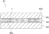
- FIG. 7 is a cross-sectional view schematically showing a connection structure using the conductive particles according to the first embodiment of the present invention.
- connection structure 81 shown in FIG. 7 includes a first connection target member 82, a second connection target member 83, and a connection portion connecting the first connection target member 82 and the second connection target member 83.
- the connection portion 84 is formed of a conductive material including the conductive particles 1.
- the connection portion 84 is preferably formed by curing a conductive material including a plurality of conductive particles 1.
- the conductive particles 1 are schematically illustrated for convenience of illustration.
- the conductive particles 11, 21, 31, 41 or 51 may be used instead of the conductive particles 1.
- the first connection target member 82 has a plurality of first electrodes 82a on the surface (upper surface).
- the second connection target member 83 has a plurality of second electrodes 83a on the surface (lower surface).
- the first electrode 82a and the second electrode 83a are electrically connected by one or more conductive particles 1. Therefore, the first connection target member 82 and the second connection target member 83 are electrically connected by the conductive portion of the conductive particles 1.
- the method of manufacturing the connection structure is not particularly limited.
- the conductive material is arranged between the first connection target member and the second connection target member, and after obtaining a laminate, the laminate is heated and pressed. Method and the like.
- the pressure of the thermocompression bonding is preferably at least 40 MPa, more preferably at least 60 MPa, preferably at most 90 MPa, more preferably at most 70 MPa.
- the heating temperature of the thermocompression bonding is preferably 80 ° C. or higher, more preferably 100 ° C. or higher, preferably 140 ° C. or lower, more preferably 120 ° C. or lower.
- the reliability of conduction between the electrodes can be further improved.
- the conductive particles have the insulating particles, the insulating particles can be easily detached from the surface of the conductive particles at the time of conductive connection.
- the conductive particles when the laminate is heated and pressurized, the conductive particles are present between the first electrode and the second electrode.
- the above insulating particles can be eliminated.
- the conductive particles, the insulating particles present between the first electrode and the second electrode, from the surface of the conductive particles Easily detached.
- some of the insulating particles may be detached from the surface of the conductive particles, and the surface of the conductive portion may be partially exposed. A portion where the surface of the conductive part is exposed contacts the first electrode and the second electrode, thereby electrically connecting the first electrode and the second electrode via the conductive particles. be able to.
- the first connection target member and the second connection target member are not particularly limited.
- the first connection target member and the second connection target member include electronic components such as a semiconductor chip, a semiconductor package, an LED chip, an LED package, a capacitor and a diode, a resin film, a printed board, and a flexible board.
- Examples include electronic components such as a printed circuit board, a flexible flat cable, a rigid flexible substrate, a circuit board such as a glass epoxy substrate and a glass substrate. It is preferable that the first connection target member and the second connection target member are electronic components.
- Examples of the electrodes provided on the connection target member include metal electrodes such as a gold electrode, a nickel electrode, a tin electrode, an aluminum electrode, a copper electrode, a molybdenum electrode, a silver electrode, a SUS electrode, and a tungsten electrode.
- the electrode is preferably a gold electrode, a nickel electrode, a tin electrode, a silver electrode, or a copper electrode.
- the electrode is preferably an aluminum electrode, a copper electrode, a molybdenum electrode, a silver electrode, or a tungsten electrode.
- the electrode When the electrode is an aluminum electrode, the electrode may be an electrode formed only of aluminum, or may be an electrode in which an aluminum layer is laminated on a surface of a metal oxide layer.
- the material of the metal oxide layer include indium oxide doped with a trivalent metal element and zinc oxide doped with a trivalent metal element.
- the trivalent metal element include Sn, Al, and Ga.
- Example 1 Production of Conductive Particle Main Body Particles having a particle diameter of 3 ⁇ m and formed of a copolymer resin of tetramethylolmethanetetraacrylate and divinylbenzene were prepared. After 10 parts by weight of the base particles were dispersed in 100 parts by weight of an alkaline solution containing 5% by weight of a palladium catalyst solution using an ultrasonic disperser, the solution was filtered to take out the base particles. Next, the base particles were added to 100 parts by weight of a 1% by weight solution of dimethylamine borane to activate the surfaces of the base particles.
- the dispersion was added to 500 parts by weight of distilled water and dispersed to obtain a dispersion.
- 1 part by weight of a nickel particle slurry (average particle diameter: 100 nm) was added to the above dispersion over 3 minutes to obtain a suspension containing base particles to which a core substance was attached.
- a nickel plating solution (pH 8.5) containing 0.35 mol / L of nickel sulfate, 1.38 mol / L of dimethylamine borane, and 0.5 mol / L of sodium citrate was prepared.
- the ultrasonic irradiation machine After putting the composition containing the following polymerizable compound into a 500 mL separable flask equipped with a four-mouth separable cover, a stirring blade, a three-way cock, a cooling tube, and a temperature probe, the ultrasonic irradiation machine is used. Emulsified. Thereafter, the mixture was stirred at 200 rpm and polymerized at 50 ° C. for 5 hours in a nitrogen atmosphere.
- the composition was composed of 200 parts by weight of distilled water, 5.2 parts by weight of iron oxide nanoparticles having a diameter of 30 nm (composition: maghemite or magnetite, manufactured by Sigma-Aldrich), and 2,2′-azobis ⁇ 2- [N- (2-carboxyethyl) amidino] propane (0.1 parts by weight). Further, the composition contains 0.1 parts by weight of polyoxyethylene lauryl ether (“Emulgen 106” manufactured by Kao Corporation), 1.7 parts by weight of methyl methacrylate, and 0.1 part by weight of ethylene glycol dimethacrylate. .
- the mixture After the completion of the reaction, the mixture is cooled, solid-liquid separation is performed twice by a centrifuge, excess polymerizable compound is removed by washing, and the entire surface of the soft magnetic material particles is covered by the coating formed by the polymerizable compound. Soft magnetic particles (particle diameter 50 nm) covered with the insulating layer were obtained.
- particles (A) the obtained soft magnetic particles coated with an insulating layer.
- conductive material anisotropic conductive paste 7 parts by weight of the obtained conductive particles, 25 parts by weight of bisphenol A type phenoxy resin, 4 parts by weight of fluorene type epoxy resin, and 30 parts by weight of phenol novolak type epoxy resin 30
- a conductive material anisotropic conductive paste was obtained by blending parts by weight with SI-60L (manufactured by Sanshin Chemical Industry Co., Ltd.) and defoaming and stirring for 3 minutes.
- anisotropic conductive paste was applied on the transparent glass substrate so as to have a thickness of 30 ⁇ m to form an anisotropic conductive paste layer.
- the semiconductor chip was stacked on the anisotropic conductive paste layer such that the electrodes faced each other.
- the pressure heating head is placed on the upper surface of the semiconductor chip, and the pressure of 60 MPa is applied to remove the anisotropic conductive paste layer.
- the composition was cured at 100 ° C. to obtain a connection structure.
- Examples 2 to 7, 10 to 12 and Comparative Examples 3 and 4 The type of the soft magnetic material portion, the coverage by the soft magnetic material portion, the thickness of the insulating portion, the amount of methyl methacrylate added when coating the surface of the soft magnetic material particles with the insulating layer, and the average particle size of the particles (A) Conductive particles, a conductive material, and a connection structure were obtained in the same manner as in Example 1, except that the settings were as shown in Table 1 below.
- Example 10 permalloy particles having an average particle diameter of 30 nm formed by a dry pulverizer such as a hammer mill and a ball mill were used instead of the iron oxide nanoparticles.
- Example 12 permezur particles (average particle diameter: 30 nm) obtained by molding permezur powder (manufactured by Daido Steel Co., Ltd.) with a dry pulverizer of a hammer mill and a ball mill were used.
- Comparative Example 4 a nickel slurry having an average particle diameter of 30 nm was used.
- the coverage by the soft magnetic material portions of Examples 2 to 7, 10 to 12 and Comparative Examples 3 and 4 was such that 10% by weight of the particles (A) was used when the conductive particles with the soft magnetic particles coated with the insulating layer were prepared. It was adjusted by changing the amount of the aqueous dispersion added.
- Example 8 (1) Production of Conductive Particle Main Body In the same manner as in Example 1, a conductive particle main body was produced.
- the ultrasonic irradiation machine After putting the composition containing the following polymerizable compound into a 500 mL separable flask equipped with a four-mouth separable cover, a stirring blade, a three-way cock, a cooling tube, and a temperature probe, the ultrasonic irradiation machine is used. Emulsified. Thereafter, the mixture was stirred at 200 rpm and polymerized at 50 ° C. for 5 hours in a nitrogen atmosphere.
- the above composition was prepared by adding 200 parts by weight of distilled water, 20 parts by weight of the obtained conductive particles, and 0.01 part by weight of 2,2′-azobis ⁇ 2- [N- (2-carboxyethyl) amidino] propane ⁇ And parts.
- the composition contains 0.1 parts by weight of polyoxyethylene lauryl ether (“Emulgen 106” manufactured by Kao Corporation), 0.1 parts by weight of methyl methacrylate, and 0.1 parts by weight of ethylene glycol dimethacrylate. .
- the mixture is cooled, solid-liquid separation is performed twice with a centrifuge, excess polymerizable compound is removed by washing, and the entire surface of the conductive particle body is covered by the coating formed by the polymerizable compound.
- the covered insulating part-covered conductive particles (the thickness of the insulating layer was 50 nm) were obtained.
- Iron oxide nanoparticles having a diameter of 30 nm were dispersed in distilled water under ultrasonic irradiation to obtain a 10% by weight aqueous dispersion. 10 parts by weight of the obtained insulating portion-coated conductive particles were dispersed in 100 parts by weight of distilled water, 1 part by weight of a 10% by weight aqueous dispersion of iron oxide nanoparticles was added, and the mixture was stirred at room temperature for 8 hours.
- conductive particles conductive particles including an insulating layer and soft magnetic material particles
- iron oxide nanoparticles are attached to insulating portion-coated conductive particles.
- connection structure was obtained in the same manner as in Example 1 except that the obtained conductive material was used.
- Insulating particles coated with soft magnetic particles Insulating particles were formed as follows.
- Example 1 The conductive particle main body of Example 1 was prepared as conductive particles. A conductive material and a connection structure were obtained in the same manner as in Example 1 except that the conductive particles were used.
- the obtained conductive particles are observed from one direction with a scanning electron microscope (SEM), and the outer peripheral portion of the surface of the conductive portion occupies the entire area within the circle of the outer peripheral portion of the surface of the conductive portion in the observation image. It was calculated from the total area of the soft magnetic portions in the circle. The coverage of the soft magnetic material portion was calculated as an average coverage obtained by observing 20 conductive particles and averaging the measurement results of each conductive particle.
- SEM scanning electron microscope
- the conductive particles obtained in Examples 1 to 7, and 10 to 12 exhibited lower connection resistance than the conductive particles obtained in Example 9. This is because, in the conductive particles of Example 9, the average particle diameter of the soft magnetic particle-coated insulating particles in which iron oxide nanoparticles having an average particle diameter of 30 nm adhere to insulating particles having an average particle diameter of 300 nm (300 nm). On the other hand, in the conductive particles of Examples 1 to 7, 10 to 12, the average particle diameter of the soft magnetic particles coated with the insulating layer is small (the average particle diameter of 50 to 130 nm).
Landscapes
- Physics & Mathematics (AREA)
- Chemical & Material Sciences (AREA)
- Dispersion Chemistry (AREA)
- Spectroscopy & Molecular Physics (AREA)
- Non-Insulated Conductors (AREA)
- Conductive Materials (AREA)
- Adhesives Or Adhesive Processes (AREA)
Abstract
Description
本発明に係る導電性粒子は、基材粒子と、上記基材粒子の表面上に配置された導電部とを備える。本発明に係る導電性粒子では、残留磁化の飽和磁化に対する比が、0.6以下である。
ρ:導電性粒子の粒子径の標準偏差
Dn:導電性粒子の粒子径の平均値
上記基材粒子としては、樹脂粒子、金属粒子を除く無機粒子、有機無機ハイブリッド粒子及び金属粒子等が挙げられる。上記基材粒子は、金属粒子を除く基材粒子であることが好ましく、樹脂粒子、金属粒子を除く無機粒子又は有機無機ハイブリッド粒子であることがより好ましい。上記基材粒子は、コアと、該コアの表面上に配置されたシェルとを備えるコアシェル粒子であってもよい。上記コアが有機コアであってもよく、上記シェルが無機シェルであってもよい。
上記導電部は、金属を含むことが好ましい。上記導電部を構成する金属は、特に限定されない。上記金属としては、例えば、金、銀、銅、白金、パラジウム、亜鉛、鉛、アルミニウム、コバルト、インジウム、ニッケル、クロム、チタン、アンチモン、ビスマス、ゲルマニウム及びカドミウム、並びにこれらの合金等が挙げられる。また、上記金属として、錫ドープ酸化インジウム(ITO)を用いてもよい。上記金属は、軟質磁性体であってもよい。上記金属は1種のみが用いられてもよく、2種以上が併用されてもよい。電極間の接続抵抗をより一層低くする観点からは、錫を含む合金、ニッケル、パラジウム、銅又は金が好ましく、ニッケル又はパラジウムがより好ましい。なお、本明細書において導電部とは、導電部を構成する材料と同じ材料を用いて粉体試料を作製し、三菱化学社製「粉体抵抗率測定システム」を用いて該粉体試料の体積抵抗値を測定したときに、該体積抵抗値が0.005Ω・cm以下である部分と定義される。
上記導電性粒子は、上記導電部の外表面に複数の突起を有することが好ましい。導電性粒子により接続される電極の表面には、酸化被膜が形成されていることが多い。導電部の表面に突起を有する導電性粒子を用いた場合には、電極間に導電性粒子を配置して圧着させることにより、突起により上記酸化被膜を効果的に排除できる。このため、電極と導電部とがより一層確実に接触し、電極間の接続抵抗がより一層低くなる。さらに、電極間の接続時に、導電性粒子の突起によって、導電性粒子と電極との間の絶縁性粒子を効果的に排除できる。このため、電極間の導通信頼性がより一層高くなる。
上記導電性粒子は、上記導電部の外表面上に配置された複数の絶縁性粒子を備えることが好ましい。この場合には、上記導電性粒子を電極間の接続に用いると、隣接する電極間の短絡を防止できる。具体的には、複数の導電性粒子が接触したときに、複数の電極間に絶縁性粒子が存在するので、上下の電極間ではなく横方向に隣り合う電極間の短絡を防止できる。なお、電極間の接続の際に、2つの電極で導電性粒子を加圧することにより、導電性粒子の導電部と電極との間の絶縁性粒子を容易に排除できる。さらに、導電部の外表面に複数の突起を有する導電性粒子である場合には、導電性粒子の導電部と電極との間の絶縁性粒子をより一層容易に排除できる。
上記導電性粒子は、上記導電部の外表面上に配置された軟質磁性体部を備えることが好ましい。上記導電性粒子が、上記軟質磁性体部を備えていると、上記導電部の導電性を損なうことなく、上記導電性粒子の残留磁化をより一層効果的に低減することができる。結果として、電極間の接続抵抗をより一層効果的に低くすることができ、かつ、磁性凝集をより一層効果的に抑制することができる。なお、本明細書において軟質磁性体部とは、外部磁場の影響下では磁化されるが、外部磁場を取り除くと速やかに磁力を失う部分と定義される。上記軟質磁性体部は、飽和磁化が0.00A/mを超え、かつ残留磁化の飽和磁化に対する比(残留磁化/飽和磁化)が0.3未満であることが好ましい。上記軟質磁性体部の飽和磁化及び上記比(残留磁化/飽和磁化)は、以下の手順に従って測定することができる。上記軟質磁性体部を構成する材料と同じ材料を用いて粉体試料を作製する。該粉体試料を導電性粒子の残留磁化及び飽和磁化を測定するのと同様の手順で、振動試料型磁力計(東栄科学産業社製「PV-300-5」)を用いて測定する。得られた飽和磁化及び残留磁化から、上記軟質磁性体部の飽和磁化及び上記比(残留磁化/飽和磁化)が得られる。
上記導電性粒子は、上記導電部と上記軟質磁性体部との間に配置された絶縁部を備えることが好ましい。上記導電性粒子では、上記軟質磁性体部が、上記絶縁部を介して上記導電部の外表面に配置されていることが好ましい。上記軟質磁性体部は、上記導電部と接触していないことが好ましい。上記絶縁部は、上記導電部と上記軟質磁性体部との間に配置されていることが好ましい。上記導電性粒子が上記の好ましい態様を満足すると、電極間の接続抵抗をより一層効果的に低くすることができ、かつ、磁性凝集をより一層効果的に抑制することができる。
本発明に係る導電材料は、上述した導電性粒子と、バインダー樹脂とを含む。上記導電性粒子は、バインダー樹脂中に分散されて用いられることが好ましく、バインダー樹脂中に分散されて導電材料として用いられることが好ましい。上記導電材料は、異方性導電材料であることが好ましい。上記導電材料は、電極間の電気的な接続に用いられることが好ましい。上記導電材料は回路接続用導電材料であることが好ましい。上記導電材料では、上述した導電性粒子が用いられているので、電極間の絶縁信頼性及び導通信頼性をより一層高めることができる。上記導電材料では、上述した導電性粒子が用いられているので、電極間の接続抵抗をより一層効果的に低くすることができ、かつ、磁性凝集をより一層効果的に抑制することができる。
本発明に係る接続構造体は、第1の電極を表面に有する第1の接続対象部材と、第2の電極を表面に有する第2の接続対象部材と、上記第1の接続対象部材と、上記第2の接続対象部材とを接続している接続部とを備える。本発明に係る接続構造体では、上記接続部の材料が、上述した導電性粒子であるか、又は上記導電性粒子とバインダー樹脂とを含む導電材料(上述した導電材料)である。本発明に係る接続構造体では、上記第1の電極と上記第2の電極とが、上記導電性粒子における上記導電部により電気的に接続されている。
(1)導電性粒子本体の作製
粒子径が3μmのテトラメチロールメタンテトラアクリレートとジビニルベンゼンとの共重合樹脂により形成された基材粒子を用意した。パラジウム触媒液を5重量%含むアルカリ溶液100重量部に、基材粒子10重量部を、超音波分散器を用いて分散させた後、溶液をろ過することにより、基材粒子を取り出した。次いで、基材粒子をジメチルアミンボラン1重量%溶液100重量部に添加し、基材粒子の表面を活性化させた。表面が活性化された基材粒子を十分に水洗した後、蒸留水500重量部に加え、分散させることにより、分散液を得た。次に、ニッケル粒子スラリー(平均粒子径100nm)1重量部を3分間かけて上記分散液に添加し、芯物質が付着された基材粒子を含む懸濁液を得た。
軟質磁性体粒子(軟質磁性体部)の表面を、以下のようにして絶縁層(絶縁部)で被覆した。
得られた粒子(A)を超音波照射下で蒸留水に分散させ、粒子(A)の10重量%水分散液を得た。得られた導電部を表面に有する基材粒子(導電性粒子本体)10重量部を蒸留水100重量部に分散させ、粒子(A)の10重量%水分散液1重量部を添加し、室温で8時間攪拌した。5μmのメッシュフィルターで濾過した後、さらにメタノールで洗浄、乾燥し、導電性粒子本体に粒子(A)が付着した導電性粒子を得た。
得られた導電性粒子7重量部と、ビスフェノールA型フェノキシ樹脂25重量部と、フルオレン型エポキシ樹脂4重量部と、フェノールノボラック型エポキシ樹脂30重量部と、SI-60L(三新化学工業社製)とを配合して、3分間脱泡及び攪拌することで、導電材料(異方性導電ペースト)を得た。
L/Sが10μm/10μmであるIZO電極パターン(第1の電極、電極表面の金属のビッカース硬度100Hv)が上面に形成された透明ガラス基板を用意した。また、L/Sが10μm/10μmであるAu電極パターン(第2の電極、電極表面の金属のビッカース硬度50Hv)が下面に形成された半導体チップを用意した。
軟質磁性体部の種類、軟質磁性体部による被覆率、絶縁部の厚み、軟質磁性体粒子の表面を絶縁層で被覆する際のメタクリル酸メチルの添加量及び粒子(A)の平均粒子径を、下記の表1に示すように設定したこと以外は実施例1と同様にして、導電性粒子、導電材料及び接続構造体を得た。
(1)導電性粒子本体の作製
実施例1と同様にして、導電性粒子本体を作製した。
導電性粒子本体の表面を、以下のようにして絶縁層(絶縁部)で被覆した。
絶縁部被覆導電性粒子における絶縁層の表面を、以下のようにして軟質磁性体粒子(軟質磁性体部)で被覆した。
得られた導電性粒子を用いたこと以外は、実施例1と同様にして、導電材料を得た。
得られた導電材料を用いたこと以外は、実施例1と同様にして、接続構造体を得た。
(1)導電性粒子本体の作製
実施例1と同様にして、導電性粒子本体を作製した。
以下のようにして絶縁性粒子を形成した。
導電性粒子本体の表面を、以下のようにして軟質磁性体粒子被覆絶縁性粒子で被覆した。
得られた導電性粒子を用いたこと以外は、実施例1と同様にして、導電材料を得た。
得られた導電材料を用いたこと以外は、実施例1と同様にして、接続構造体を得た。
実施例1の導電性粒子本体を導電性粒子として用意した。この導電性粒子を用いたこと以外は実施例1と同様にして、導電材料、及び接続構造体を得た。
(1)導電性粒子本体の作製
実施例1と同様にして、導電性粒子本体を作製した。
導電性粒子本体の表面を、以下のようにして軟質磁性体粒子で被覆した。
得られた導電性粒子を用いたこと以外は、実施例1と同様にして、導電材料を得た。
得られた導電材料を用いたこと以外は、実施例1と同様にして、接続構造体を得た。
(1)導電性粒子の残留磁化及び飽和磁化
ニッケル粉を封入したカプセルを装置の校正試料として使用し、振動試料型磁力計(東栄科学産業社製「PV-300-5」)の校正を行った。得られた導電性粒子をカプセルに秤量し、サンプルホルダーに取り付けた。該サンプルホルダーを磁力計本体に設置し、温度20℃(定温)、最大印加磁界20kOe、速度3分/loopの条件下での測定により、磁化曲線を得た。得られた磁化曲線から、導電性粒子の残留磁化及び飽和磁化を求めた。
得られた導電性粒子の導電部の表面積全体に占める導電部の表面の軟質磁性体部により覆われている部分の面積(軟質磁性体部による被覆率)を測定した。
得られた導電性粒子の絶縁部の厚みを、以下のようにして測定した。
得られた導電材料を観察し、導電性粒子の磁性凝集が発生しているか否かを確認した。導電性粒子の磁性凝集を下記の条件で判定した。
○○:導電性粒子の磁性凝集が発生していない
○:導電性粒子の磁性凝集が僅かに発生しているが抑制効果が認められる
×:導電性粒子の磁性凝集が発生している
得られた20個の接続構造体の上下の電極間の接続抵抗をそれぞれ、4端子法により測定した。なお、電圧=電流×抵抗の関係から、一定の電流を流した時の電圧を測定することにより接続抵抗を求めることができる。接続抵抗を下記の基準で判定した。
○○○:接続抵抗が1.5Ω以下
○○:接続抵抗が1.5Ωを超え2.0Ω以下
○:接続抵抗が2.0Ωを超え5.0Ω以下
△:接続抵抗が5.0Ωを超え10Ω以下
×:接続抵抗が10Ωを超える
上記(5)導通信頼性の評価で得られた20個の接続構造体において、隣接する電極間のリークの有無を、テスターで抵抗値を測定することにより評価した。絶縁信頼性を下記の基準で評価した。
○○○:抵抗値が108Ω以上の接続構造体の個数が、20個
○○:抵抗値が108Ω以上の接続構造体の個数が、18個以上20個未満
○:抵抗値が108Ω以上の接続構造体の個数が、15個以上18個未満
△:抵抗値が108Ω以上の接続構造体の個数が、10個以上15個未満
×:抵抗値が108Ω以上の接続構造体の個数が、10個未満


2…基材粒子
3…導電部
11…導電性粒子
12…軟質磁性体部
13…絶縁性粒子
21…導電性粒子
22…絶縁部
31…導電性粒子
32…絶縁部
41…導電性粒子
42…絶縁部
51…導電性粒子
52…絶縁部
61…導電部
62…芯物質
63…突起
81…接続構造体
82…第1の接続対象部材
82a…第1の電極
83…第2の接続対象部材
83a…第2の電極
84…接続部
Claims (11)
- 基材粒子と、前記基材粒子の表面上に配置された導電部とを備え、
残留磁化の飽和磁化に対する比が、0.6以下である、導電性粒子。 - 前記残留磁化が、0.02A/m以下である、請求項1に記載の導電性粒子。
- 前記導電部の外表面上に配置された軟質磁性体部を備える、請求項1又は2に記載の導電性粒子。
- 前記導電部と前記軟質磁性体部との間に配置された絶縁部を備え、
前記軟質磁性体部が、前記絶縁部を介して前記導電部の外表面上に配置されている、請求項3に記載の導電性粒子。 - 前記導電部と前記軟質磁性体部との離れている距離が、10nm以上500nm以下である、請求項4に記載の導電性粒子。
- 前記軟質磁性体部を複数備え、
複数の前記軟質磁性体部が離れて、前記導電部の外表面上に配置されている、請求項3~5のいずれか1項に記載の導電性粒子。 - 前記導電部の表面積全体に占める前記導電部の表面の前記軟質磁性体部により覆われている部分の面積が、30%以上である、請求項3~6のいずれか1項に記載の導電性粒子。
- 前記導電部の表面積全体に占める前記導電部の表面の前記軟質磁性体部により覆われている部分の面積が、40%以上である、請求項7に記載の導電性粒子。
- 前記導電部の外表面上に配置された複数の絶縁性粒子を備える、請求項1~8のいずれか1項に記載の導電性粒子。
- 請求項1~9のいずれか1項に記載の導電性粒子と、バインダー樹脂とを含む、導電材料。
- 第1の電極を表面に有する第1の接続対象部材と、
第2の電極を表面に有する第2の接続対象部材と、
前記第1の接続対象部材と、前記第2の接続対象部材とを接続している接続部とを備え、
前記接続部の材料が、請求項1~9のいずれか1項に記載の導電性粒子であるか、又は前記導電性粒子とバインダー樹脂とを含む導電材料であり、
前記第1の電極と前記第2の電極とが、前記導電性粒子における前記導電部により電気的に接続されている、接続構造体。
Priority Applications (4)
| Application Number | Priority Date | Filing Date | Title |
|---|---|---|---|
| JP2020527481A JP7280880B2 (ja) | 2018-06-25 | 2019-06-21 | 導電性粒子、導電材料及び接続構造体 |
| KR1020207031840A KR102647120B1 (ko) | 2018-06-25 | 2019-06-21 | 도전성 입자, 도전 재료 및 접속 구조체 |
| CN202310216345.XA CN116189963A (zh) | 2018-06-25 | 2019-06-21 | 导电性粒子、导电材料以及连接结构体 |
| CN201980040888.2A CN112313758B (zh) | 2018-06-25 | 2019-06-21 | 导电性粒子、导电材料以及连接结构体 |
Applications Claiming Priority (2)
| Application Number | Priority Date | Filing Date | Title |
|---|---|---|---|
| JP2018119894 | 2018-06-25 | ||
| JP2018-119894 | 2018-06-25 |
Publications (1)
| Publication Number | Publication Date |
|---|---|
| WO2020004273A1 true WO2020004273A1 (ja) | 2020-01-02 |
Family
ID=68986895
Family Applications (1)
| Application Number | Title | Priority Date | Filing Date |
|---|---|---|---|
| PCT/JP2019/024743 Ceased WO2020004273A1 (ja) | 2018-06-25 | 2019-06-21 | 導電性粒子、導電材料及び接続構造体 |
Country Status (5)
| Country | Link |
|---|---|
| JP (1) | JP7280880B2 (ja) |
| KR (1) | KR102647120B1 (ja) |
| CN (2) | CN116189963A (ja) |
| TW (1) | TWI820157B (ja) |
| WO (1) | WO2020004273A1 (ja) |
Cited By (4)
| Publication number | Priority date | Publication date | Assignee | Title |
|---|---|---|---|---|
| US20200340936A1 (en) * | 2019-04-26 | 2020-10-29 | Nabtesco Corporation | Sensor |
| WO2021246523A1 (ja) * | 2020-06-04 | 2021-12-09 | 積水化学工業株式会社 | 導電性粒子、導電材料及び接続構造体 |
| CN114121470A (zh) * | 2020-08-25 | 2022-03-01 | 株式会社村田制作所 | 磁粉的制造方法、压粉成型体的制造方法、磁粉及压粉成型体 |
| US20220178857A1 (en) * | 2019-04-26 | 2022-06-09 | Nabtesco Corporation | Sensor |
Families Citing this family (1)
| Publication number | Priority date | Publication date | Assignee | Title |
|---|---|---|---|---|
| US12002159B2 (en) * | 2021-06-09 | 2024-06-04 | Dassault Systemes Americas Corp. | Prediction of mechanical properties of sedimentary rocks based on a grain to grain parametric cohesive contact model |
Citations (4)
| Publication number | Priority date | Publication date | Assignee | Title |
|---|---|---|---|---|
| JPH05190014A (ja) * | 1992-01-09 | 1993-07-30 | Sekisui Fine Chem Kk | 電極接続用導電性微球体 |
| JP2011175951A (ja) * | 2009-08-06 | 2011-09-08 | Hitachi Chem Co Ltd | 導電性微粒子及び異方性導電材料 |
| JP2012142223A (ja) * | 2011-01-05 | 2012-07-26 | Sekisui Chem Co Ltd | 導電性粒子、異方性導電材料及び接続構造体 |
| WO2019027023A1 (ja) * | 2017-08-03 | 2019-02-07 | パウダーテック株式会社 | 複合粒子、粉末、樹脂組成物および成形体 |
Family Cites Families (11)
| Publication number | Priority date | Publication date | Assignee | Title |
|---|---|---|---|---|
| JP2002157918A (ja) * | 2000-11-17 | 2002-05-31 | Jsr Corp | 導電性複合粒子およびそれを用いた応用製品 |
| DE60310739T2 (de) * | 2002-08-27 | 2007-10-11 | Jsr Corp. | Anisotrope leitfähige folie und impedanzmesssonde |
| CA2418497A1 (en) * | 2003-02-05 | 2004-08-05 | Patrick Lemieux | High performance soft magnetic parts made by powder metallurgy for ac applications |
| JP4967482B2 (ja) * | 2006-02-27 | 2012-07-04 | 日立化成工業株式会社 | 導電粒子、接着剤組成物及び回路接続材料 |
| CN101260243A (zh) * | 2008-04-30 | 2008-09-10 | 杨力 | 一种高分子复合导电材料电线芯材及制备方法 |
| IT1399315B1 (it) * | 2010-04-08 | 2013-04-16 | Cappelli | Procedimento per disporre su una qualsiasi superficie verniciabile, dei circuiti conduttori e/o generatori di cariche elettriche e circuiti realizzati con tale procedimento. |
| JP5757228B2 (ja) * | 2011-12-19 | 2015-07-29 | デクセリアルズ株式会社 | 異方性導電接着剤、その製造方法、接続構造体及びその製造方法 |
| JP6079425B2 (ja) * | 2012-05-16 | 2017-02-15 | 日立化成株式会社 | 導電粒子、異方性導電接着剤フィルム及び接続構造体 |
| JP6369750B2 (ja) * | 2013-09-10 | 2018-08-08 | 日立金属株式会社 | 積層配線膜およびその製造方法ならびにNi合金スパッタリングターゲット材 |
| KR101959536B1 (ko) * | 2016-04-05 | 2019-03-18 | 주식회사 아이에스시 | 이종의 입자가 혼합된 도전성 입자를 포함하는 이방도전성 시트 |
| JPWO2019159799A1 (ja) * | 2018-02-13 | 2021-03-04 | パウダーテック株式会社 | 複合粒子、粉末、樹脂組成物および成形体 |
-
2019
- 2019-06-21 WO PCT/JP2019/024743 patent/WO2020004273A1/ja not_active Ceased
- 2019-06-21 JP JP2020527481A patent/JP7280880B2/ja active Active
- 2019-06-21 CN CN202310216345.XA patent/CN116189963A/zh active Pending
- 2019-06-21 KR KR1020207031840A patent/KR102647120B1/ko active Active
- 2019-06-21 CN CN201980040888.2A patent/CN112313758B/zh active Active
- 2019-06-25 TW TW108122094A patent/TWI820157B/zh active
Patent Citations (4)
| Publication number | Priority date | Publication date | Assignee | Title |
|---|---|---|---|---|
| JPH05190014A (ja) * | 1992-01-09 | 1993-07-30 | Sekisui Fine Chem Kk | 電極接続用導電性微球体 |
| JP2011175951A (ja) * | 2009-08-06 | 2011-09-08 | Hitachi Chem Co Ltd | 導電性微粒子及び異方性導電材料 |
| JP2012142223A (ja) * | 2011-01-05 | 2012-07-26 | Sekisui Chem Co Ltd | 導電性粒子、異方性導電材料及び接続構造体 |
| WO2019027023A1 (ja) * | 2017-08-03 | 2019-02-07 | パウダーテック株式会社 | 複合粒子、粉末、樹脂組成物および成形体 |
Cited By (12)
| Publication number | Priority date | Publication date | Assignee | Title |
|---|---|---|---|---|
| US20200340936A1 (en) * | 2019-04-26 | 2020-10-29 | Nabtesco Corporation | Sensor |
| US20220178857A1 (en) * | 2019-04-26 | 2022-06-09 | Nabtesco Corporation | Sensor |
| US11499931B2 (en) * | 2019-04-26 | 2022-11-15 | Nabtesco Corporation | Sensor |
| US20230035518A1 (en) * | 2019-04-26 | 2023-02-02 | Nabtesco Corporation | Sensor |
| US12038400B2 (en) | 2019-04-26 | 2024-07-16 | Nabtesco Corporation | Sensor |
| US12270775B2 (en) * | 2019-04-26 | 2025-04-08 | Nabtesco Corporation | Sensor |
| WO2021246523A1 (ja) * | 2020-06-04 | 2021-12-09 | 積水化学工業株式会社 | 導電性粒子、導電材料及び接続構造体 |
| JPWO2021246523A1 (ja) * | 2020-06-04 | 2021-12-09 | ||
| CN115699218A (zh) * | 2020-06-04 | 2023-02-03 | 积水化学工业株式会社 | 导电性粒子、导电材料和连接结构体 |
| JP7701921B2 (ja) | 2020-06-04 | 2025-07-02 | 積水化学工業株式会社 | 導電性粒子、導電材料、異方性導電材料及び接続構造体 |
| KR102949959B1 (ko) * | 2020-06-04 | 2026-04-08 | 세키스이가가쿠 고교가부시키가이샤 | 도전성 입자, 도전 재료 및 접속 구조체 |
| CN114121470A (zh) * | 2020-08-25 | 2022-03-01 | 株式会社村田制作所 | 磁粉的制造方法、压粉成型体的制造方法、磁粉及压粉成型体 |
Also Published As
| Publication number | Publication date |
|---|---|
| JPWO2020004273A1 (ja) | 2021-08-05 |
| KR20210022541A (ko) | 2021-03-03 |
| CN112313758B (zh) | 2023-02-28 |
| JP7280880B2 (ja) | 2023-05-24 |
| CN112313758A (zh) | 2021-02-02 |
| KR102647120B1 (ko) | 2024-03-14 |
| CN116189963A (zh) | 2023-05-30 |
| TW202015074A (zh) | 2020-04-16 |
| TWI820157B (zh) | 2023-11-01 |
Similar Documents
| Publication | Publication Date | Title |
|---|---|---|
| JP7280880B2 (ja) | 導電性粒子、導電材料及び接続構造体 | |
| JP5216165B1 (ja) | 導電性粒子、導電材料及び接続構造体 | |
| JP6034177B2 (ja) | 導電性粒子、導電材料及び接続構造体 | |
| JP6276351B2 (ja) | 導電性粒子、導電材料及び接続構造体 | |
| JP6084868B2 (ja) | 導電性粒子、導電材料及び接続構造体 | |
| WO2019194135A1 (ja) | 絶縁性粒子付き導電性粒子、導電材料及び接続構造体 | |
| JP7463069B2 (ja) | 導電性粒子、導電材料、接続構造体及び接続構造体の製造方法 | |
| WO2017051842A1 (ja) | 導電性粒子、導電材料、および接続構造体 | |
| JP6200318B2 (ja) | 導電性粒子、導電材料及び接続構造体 | |
| JP6478308B2 (ja) | 導電性粒子、導電材料及び接続構造体 | |
| JPWO2020175691A1 (ja) | 導電性粒子、導電材料及び接続構造体 | |
| JP7701921B2 (ja) | 導電性粒子、導電材料、異方性導電材料及び接続構造体 | |
| JP6457743B2 (ja) | 接続構造体 | |
| JP2018137225A (ja) | 導電性粒子、導電材料及び接続構造体 | |
| JP7271543B2 (ja) | 絶縁性粒子付き導電性粒子、導電材料及び接続構造体 | |
| JP6441555B2 (ja) | 導電性粒子、導電材料及び接続構造体 | |
| JP7132112B2 (ja) | 導電フィルム及び接続構造体 | |
| WO2022260158A1 (ja) | 被覆粒子、樹脂組成物及び接続構造体 | |
| WO2022260159A1 (ja) | 被覆粒子、被覆粒子の製造方法、樹脂組成物及び接続構造体 | |
| JP6333624B2 (ja) | 接続構造体 | |
| JP2015056306A (ja) | 導電性粒子、導電材料及び接続構造体 | |
| JP2020013787A (ja) | 導電材料及び接続構造体 | |
| WO2019194133A1 (ja) | 絶縁性粒子付き導電性粒子、絶縁性粒子付き導電性粒子の製造方法、導電材料及び接続構造体 | |
| WO2019194134A1 (ja) | 絶縁性粒子付き導電性粒子、絶縁性粒子付き導電性粒子の製造方法、導電材料及び接続構造体 |
Legal Events
| Date | Code | Title | Description |
|---|---|---|---|
| 121 | Ep: the epo has been informed by wipo that ep was designated in this application |
Ref document number: 19825852 Country of ref document: EP Kind code of ref document: A1 |
|
| ENP | Entry into the national phase |
Ref document number: 2020527481 Country of ref document: JP Kind code of ref document: A |
|
| ENP | Entry into the national phase |
Ref document number: 20207031840 Country of ref document: KR Kind code of ref document: A |
|
| NENP | Non-entry into the national phase |
Ref country code: DE |
|
| 122 | Ep: pct application non-entry in european phase |
Ref document number: 19825852 Country of ref document: EP Kind code of ref document: A1 |