WO2020003698A1 - 出力ノイズ低減装置 - Google Patents
出力ノイズ低減装置 Download PDFInfo
- Publication number
- WO2020003698A1 WO2020003698A1 PCT/JP2019/016276 JP2019016276W WO2020003698A1 WO 2020003698 A1 WO2020003698 A1 WO 2020003698A1 JP 2019016276 W JP2019016276 W JP 2019016276W WO 2020003698 A1 WO2020003698 A1 WO 2020003698A1
- Authority
- WO
- WIPO (PCT)
- Prior art keywords
- conductive bar
- lead member
- magnetic core
- output
- mounting board
- Prior art date
- Legal status (The legal status is an assumption and is not a legal conclusion. Google has not performed a legal analysis and makes no representation as to the accuracy of the status listed.)
- Ceased
Links
Images


Classifications
-
- H—ELECTRICITY
- H01—ELECTRIC ELEMENTS
- H01F—MAGNETS; INDUCTANCES; TRANSFORMERS; SELECTION OF MATERIALS FOR THEIR MAGNETIC PROPERTIES
- H01F17/00—Fixed inductances of the signal type
- H01F17/04—Fixed inductances of the signal type with magnetic core
- H01F17/06—Fixed inductances of the signal type with magnetic core with core substantially closed in itself, e.g. toroid
-
- H—ELECTRICITY
- H01—ELECTRIC ELEMENTS
- H01F—MAGNETS; INDUCTANCES; TRANSFORMERS; SELECTION OF MATERIALS FOR THEIR MAGNETIC PROPERTIES
- H01F27/00—Details of transformers or inductances, in general
- H01F27/06—Mounting, supporting or suspending transformers, reactors or choke coils not being of the signal type
-
- H—ELECTRICITY
- H01—ELECTRIC ELEMENTS
- H01F—MAGNETS; INDUCTANCES; TRANSFORMERS; SELECTION OF MATERIALS FOR THEIR MAGNETIC PROPERTIES
- H01F27/00—Details of transformers or inductances, in general
- H01F27/28—Coils; Windings; Conductive connections
- H01F27/29—Terminals; Tapping arrangements for signal inductances
-
- H—ELECTRICITY
- H01—ELECTRIC ELEMENTS
- H01F—MAGNETS; INDUCTANCES; TRANSFORMERS; SELECTION OF MATERIALS FOR THEIR MAGNETIC PROPERTIES
- H01F27/00—Details of transformers or inductances, in general
- H01F27/28—Coils; Windings; Conductive connections
- H01F27/32—Insulating of coils, windings, or parts thereof
-
- H—ELECTRICITY
- H03—ELECTRONIC CIRCUITRY
- H03H—IMPEDANCE NETWORKS, e.g. RESONANT CIRCUITS; RESONATORS
- H03H7/00—Multiple-port networks comprising only passive electrical elements as network components
- H03H7/01—Frequency selective two-port networks
Definitions
- the technology disclosed in the present application relates to an output noise reduction device that suppresses noise mixed into an output signal, and more particularly to a noise reduction device including an inductance element inserted into a signal path of an output signal.
- Patent Document 1 discloses a noise filter module including a choke coil in which a conductive bar penetrates a magnetic core and a mounting substrate on which a capacitor and the like are mounted.
- a plurality of lead members are arranged along the exterior of a general-purpose module on a general-purpose module in which a magnetic core is penetrated by a conductive bar and molded with a resin material.
- a plurality of lead members connect a mounting board on which a capacitor or the like is mounted to input and output ends of both ends of the conductive bar, and connect a GND surface of the mounting board to a ground potential GND. .
- a plurality of lead members are arranged along the exterior of the general-purpose module in a general-purpose module molded with a resin material, so that the lead members are easily exposed to the atmosphere and corroded.
- the lead members are arranged along the exterior of the general-purpose module, the shape of the lead members becomes complicated, and the parts cost increases, and the lead assembling process becomes difficult, so that the production cost increases. there were.
- a connection failure may occur in the connection portion of the lead member, and the reliability as a noise filter module may be reduced.
- the technology disclosed in the present application has been proposed in view of the above problem, and reduces component costs and manufacturing costs by improving the assembling of leads and efficiently using the occupied area of the mounting board. It is another object of the present invention to provide an output noise reduction device capable of responding to a wide range of customer requests.
- an output noise reduction device that connects a mounting board to reduce noise mixed in an output signal from an electronic device, and is formed of a conductive material.
- a conductive bar having one end serving as a connection terminal for connecting to an output end of the electronic device and the other end serving as an output terminal; and a magnetic core formed of a magnetic material and having a through hole through which the conductive bar passes.
- a first lead member and a second lead member formed of a conductive member for connecting the mounting board to the connection terminal and the output terminal, wherein a first lead member and a second lead member are formed between the magnetic core of the conductive bar and the connection terminal.
- An output noise reduction device is the output noise reduction device according to the first aspect, wherein the first lead member and the second lead member are substantially perpendicular to the conductive bar toward the mounting substrate.
- the end connected to the conductive bar extends and is bent in a substantially horizontal direction, and the bent ends of the first lead member and the second lead member are located in the through holes of the magnetic core. And connected to the conductive bar.
- An output noise reduction device is the output noise reduction device according to the first or second aspect, wherein the first lead member and the second lead member are connectors connected to a mounting board.
- the first lead member and the second lead member are molded by the mold member while being connected to the conductive bar, for example, the first lead member and the second lead member Most of the first lead member and the second lead member can be covered with resin by molding up to the portion excluding the upper end of the first lead member. Thus, the first lead member and the second lead member can be prevented from being exposed to the atmosphere, and the corrosion can be suppressed.
- the lead assembling step can be simplified, so that the manufacturing cost can be reduced.
- the first lead member and the second lead member can be integrally formed, the resistance to vibration and shock at the connection between the conductive bar and the first lead member and the second lead member is also improved. In addition, the reliability of the noise filter module can be improved.
- the first lead member and the second lead member have ends connected to the conductive bar bent in the horizontal direction, and the other ends of the first lead member and the second lead member are connected to the conductive bar.
- the connection between the conductive bar and the mounting board can be minimized by connecting the conductive bar and the mounting board with each other in the direction substantially perpendicular to the mounting board. Thereby, the parasitic capacitance and the parasitic inductance of the first lead member and the second lead member can be suppressed low, and the characteristics as a noise filter module can be improved.
- the connection terminal of the conductive bar is independent of the first lead member and the second lead member. And an output terminal.
- the mounting board can be easily attached or detached.
- the mounting board can be held only by connecting the connector, screwing or the like for mounting the mounting board becomes unnecessary, so that the number of parts and the assembling work can be reduced, and as a result, the manufacturing cost can be reduced.
- FIG. 2 is a circuit diagram of an example of an output noise reduction device in which a noise filter module using the noise filter according to the first embodiment is connected to a switching power supply.
- FIG. 2 is an exploded perspective view of the noise filter according to the first embodiment.
- FIG. 3 is a perspective view illustrating a method of assembling the noise filter according to the first embodiment. It is a perspective view of the state where the noise filter of 1st Embodiment was assembled. It is a perspective view of the state where the noise filter of a 1st embodiment was molded. It is a perspective view (the 1) explaining a procedure of attaching a mounting board to a noise filter of a 1st embodiment.
- FIG. 9 is a perspective view (part 2) for explaining the procedure for attaching the mounting board to the noise filter of the first embodiment.
- FIG. 9 is a perspective view (part 2) for explaining the procedure for attaching the mounting board to the noise filter of the first embodiment.
- It is an exploded perspective view of a noise filter of a 2nd embodiment.
- FIG. 9 is a perspective view illustrating an assembled state of a noise filter according to a second embodiment. It is a perspective view of the molded state of the noise filter of a 2nd embodiment. It is an exploded perspective view of a noise filter of other embodiments.
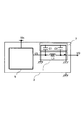
- FIG. 1 is a circuit diagram showing an example of an output noise reduction device using the noise filter 1 of the first embodiment according to the present invention.
- the noise filter module shown in FIG. 1 includes a mounting board 7 on which a capacitor and the like are mounted and the noise filter 1, and is connected between the output terminal VX and the output terminal VO of the switching power supply 5.
- the switching power supply 5 and the noise filter module are housed in a metal casing 3 made of aluminum die cast or the like.
- FIG. 1 illustrates the electrical operation and effect of the noise filter module.
- the switching power supply 5 is, for example, a power supply for a vehicle. This is a step-down switching power supply that steps down a voltage value from a main battery (not shown) that supplies a power supply voltage VIN of a drive system in a hybrid vehicle or an electric vehicle and supplies power to an auxiliary battery (not shown).
- the auxiliary battery supplies a power supply voltage to in-vehicle electrical devices such as audio devices, air conditioners, and lighting devices.
- the switching power supply 5 obtains an output of a predetermined voltage by turning on / off a power transistor (not shown) at a predetermined switching frequency f.
- a voltage fluctuates alternately between a high voltage and a low voltage at the switching frequency f.
- a current corresponding to the load current alternately intermittently flows between the power supply voltage VIN and the ground potential GND, causing a current fluctuation.
- Voltage fluctuations and current fluctuations due to the switching operation may become noise sources, causing noise to the output terminal.
- Such a noise source may propagate to the output terminal as conduction noise wrapping around via a signal path or a ground wiring, and may also propagate to the output terminal as radiation noise radiated by electromagnetic coupling such as capacitive coupling or inductive coupling.
- the radiated noise may be caused by, for example, voltage fluctuation of the internal connection. This is a case where unexpected voltage fluctuations are caused to the coupled circuit element in accordance with capacitive coupling due to a parasitic capacitance component interposed between circuit elements or between wirings. Further, it may occur with a current fluctuation of the power supply voltage VIN or the ground potential GND.
- a noise filter module is connected to the output terminal VX of the switching power supply 5.
- a choke coil L1 is provided in an output voltage path connecting an output terminal VX and an output terminal VO of the switching power supply 5, and a capacitor C1 is connected between the output terminal VX of the switching power supply 5 and the ground potential GND.
- the capacitor C2 is connected between the terminal VO and the ground potential GND.
- CLC ⁇ -type filter.
- the capacitors C1 and C2 are mounted on the component surface of the mounting board 7.
- the surface opposite to the component surface of the mounting substrate 7 is, for example, a ground surface, and is connected to the ground potential GND.
- the noise filter module can suppress noise of the switching frequency f or its harmonic frequency, which propagates in the signal path, out of the conducted noise.
- the switching frequency f in the switching power supply 5 is determined according to the power rating to be output, the specifications and ratings of each component, and the like. For example, an in-vehicle switching power supply may operate at several hundred kHz. For this reason, the switching frequency f and its harmonic frequency may overlap the frequency band of the in-vehicle AM radio, and the provision of the noise filter module makes it possible to suppress the conducted noise propagating in the signal path in these bands. .
- the switching power supply 5 and the noise filter module are housed in a metal housing 3 made of aluminum die cast or the like. Thereby, since the metal housing 3 has an electromagnetic shielding effect, propagation of radiation noise generated by the switching operation in the metal housing 3 to the output terminal VO is suppressed.
- the ground surface of the mounting board 7 is connected to the ground potential GND, the ground surface has an electromagnetic shielding effect. Is suppressed from propagating to the capacitors C1 and C2 mounted on the first and second capacitors. As a result, the performance of the noise filter module as a filter can be sufficiently exhibited.
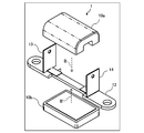
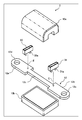
- FIG. 2 is an exploded perspective view of the noise filter 1.
- FIG. 3A is a perspective view of a method of assembling the noise filter 1
- FIG. 4 is a perspective view showing a state where the noise filter 1 is molded.
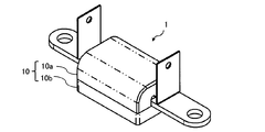
- the noise filter 1 includes a conductive bar 12, a magnetic core 10 including a magnetic core upper portion 10a and a magnetic core lower portion 10b, a lead member 13, and a lead member 14.
- the conductive bar 12 is used as an output voltage path connecting the output terminal VX and the output terminal VO of the switching power supply 5 shown in FIG.
- the conductive bar 12 has a generally flat shape, has a horizontally long shape extending in the direction of the output terminal VX and the output terminal VO of the switching power supply 5, and is formed of a metal material such as copper or carbon steel.
- Bolt portions 12a and 12b are formed at both outer ends in the extension direction with the central portion 12c interposed therebetween.
- One bolt portion 12a is provided with a bolt hole 12d for connection to the output terminal VX of the switching power supply 5, and the other bolt portion 12b is provided with a bolt hole 12e for connection to the output terminal VO.
- the bolt portion 12a is connected to the output terminal VX of the switching power supply 5 using the bolt hole 12d.
- the bolt portion 12b is an output terminal VO, and is connected to a subsequent electronic device or the like using the bolt hole 12e.
- the bolt portions 12a and 12b and the central portion 12c are arranged in the same straight line, and the conductive bar 12 is formed of a single metal member.
- the central portion 12c is slightly narrower in the width direction than the bolt portions 12a and 12b, and a magnetic core 10 composed of a magnetic core upper portion 10a and a magnetic core lower portion 10b is provided at the center of the central portion 12c. And is arranged so as to penetrate.
- the magnetic core 10 is composed of a magnetic core upper part 10a provided with a U-shaped groove 10c at the center of the lower surface in the shape of a bottom and a substantially rectangular magnetic core lower part 10b, and a magnetic material such as ferrite, for example. It is formed with.
- the magnetic core upper part 10a and the magnetic core lower part 10b are aligned as shown in FIG. 3B, so that the U-shaped groove 10c of the magnetic core upper part 10a forms a hollow part, and the conductive bar is formed in the formed hollow part. 12 penetrates, and the choke coil L1 is configured by arranging the inner side surface of the hollow portion and the central portion 12c of the conductive bar 12 so as to face each other.
- a gap (referred to as a slit) may be provided without contacting one of the left and right surfaces with respect to the conductive bar 12 with which the magnetic core upper part 10a and the magnetic core lower part 10b abut.
- a so-called core gap is formed in which a part of the path circulating in the circumferential direction with respect to the central portion 12c of the conductive bar 12 is discontinuous, and a magnetic gap composed of the magnetic core upper portion 10a and the magnetic core lower portion 10b is formed.
- the magnetic resistance in the body core 10 can be adjusted to prevent the occurrence of magnetic saturation.
- the width of the slit the magnetic resistance can be adjusted to suppress magnetic saturation, and the inductance of the choke coil L1 required for removing noise components can be secured.
- the extending direction of the conductive bar 12 corresponds to the penetrating direction penetrating the magnetic core.
- the lead members 13 and 14 are for connecting the mounting board 7 shown in FIG. 1, and are formed of a conductive metal material such as copper, nickel, or iron. As shown in FIG. 2, the lead members 13 and 14 are plate-shaped, and extend 13b and 14b extending substantially perpendicularly to the conductive bar 12 toward the mounting substrate 7, and 13a and 14a bent substantially horizontally. Is formed from. The widths 13a and 14a of the lead members 13 and 14 are substantially the same as or slightly smaller than the width of the central portion 12c of the conductive bar 12.
- the hollow portion (the U-shaped groove 10c) of the magnetic core 10 formed by combining the upper body portion 10a and the lower magnetic core portion 10b can be penetrated without interference and assembled. Further, bolt holes 13c and 14c for connecting a mounting board 7 described later are provided above the lead members 13 and 14 at 13b and 14b.
- 13a and 14a of the lead members 13 and 14 are connected to the conductive bar 12.
- the connection may be made by welding or by soldering. Alternatively, the connection may be made using a screw (not shown). Then, as shown by arrow B in FIG. 3A, the conductive bar 12 connecting the lead members 13 and 14 is sandwiched between the magnetic core upper part 10a and the magnetic core lower part 10b, and as shown in FIG. Is assembled.
- the assembled noise filter 1 is molded by a mold 20 formed of a resin material, as shown in FIG.
- a mold 20 formed of a resin material, as shown in FIG.
- most of the lead members 13 and 14 are covered with the resin by molding up to the portion excluding the upper end portions of the lead members 13 and 14 by the mold 20. Therefore, it is possible to prevent the lead members 13 and 14 from being corroded by contact with the atmosphere.
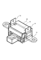
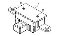
- FIG. 5A to 6B are perspective views for explaining a procedure for attaching the mounting substrate 7 to the noise filter 1.
- FIG. 5A to 6B are perspective views for explaining a procedure for attaching the mounting substrate 7 to the noise filter 1.
- concave portions 20a and 20b are provided on the upper surface of the mold 20.
- the recesses 20a and 20b have a width and depth such that the nut screws 21 and 21 are housed therein and the nut screws 21 and 21 cannot move within the recesses 20a and 20b.
- the upper ends of the lead members 13 and 14 are bent in the directions shown by arrows D and D. .
- FIG. 5B shows a state where the upper ends of the lead members 13 and 14 are bent.
- FIG. 6A after mounting screws 22, 22 are inserted into two mounting holes 7 a, 7 a provided in mounting substrate 7, inserted into bolt holes 13 c and 14 c of lead members 13 and 14, and As shown in FIG. 6B, the mounting board 7 is screwed with the screws 22 and 22 and fitted to the noise filter 1 by fitting with the nut screws 21 and 21 in the recesses 20a and 20b.
- a pattern for connecting a capacitor or the like mounted on the mounting board 7 is formed around the mounting holes 7a, 7a of the mounting board 7 in contact with the lead members 13 and 14.
- the conductive bar 12 and the mounting board 7 can be connected by the shortest lead members 13 and 14, the parasitic capacitance and the parasitic inductance of the lead members 13 and 14 can be suppressed low. . Thereby, characteristics as a noise filter module can be improved. Further, by connecting the lead members 13 and 14 to the conductive bar 12 first, the lead assembling step can be facilitated. Therefore, component costs and manufacturing costs can be reduced. In addition, since the mold 20 can be formed in a relatively simple shape, the size and shape of the mounting substrate 7 are less likely to be restricted, and it becomes possible to mount a capacitor according to the customer's request. It is possible to provide a noise filter module that can flexibly respond to the noise filter module. Also, since the lead members 13 and 14 can be integrally formed, the connection between the conductive bar 12 and the lead members 13 and 14 has improved resistance to vibration and impact, and also has improved reliability as a noise filter module. can do.
- FIG. 7 is an exploded perspective view of the noise filter 2 according to the second embodiment.
- FIG. 8A is a perspective view showing an assembled state of the noise filter 2
- FIG. 8B is a perspective view showing a state in which the noise filter 2 is molded.
- connectors 30 and 31 are employed instead of the lead members 13 and 14 described above.
- a mold formed of a resin material as shown in FIG. 8B. Molded at 40.
- four circular concave portions 40a for attaching a mounting board (not shown) are provided.
- four recesses 40a are provided, but it is sufficient that the number of recesses 40a is two or more, and the number is not limited.
- a connector having a polarity opposite to that of the connector 30 and the connector 31 is mounted on the lower surface side of the mounting board.
- the mounting board is connected to the connector 30 and the connector 31 by a connector and attached to the mold 40 by screwing or the like. If the mounting board can be held only by connector connection, screwing is not necessary. In this case, mounting and dismounting of the mounting board becomes easy, and the assembling work becomes easy.
- the switching power supply 5 is an example of an electronic device
- the noise filters 1 and 2 are an example of an output noise reduction device
- the conductive bar 12 is an example of a conductive bar
- the magnetic core 10 is an example of a magnetic core.
- the mounting substrate 7 is an example of a mounting substrate
- the lead members 13 and 14 and the connectors 30 and 31 are examples of a lead member
- the molds 20 and 40 are examples of a molding member.
- the noise filter module is a CLC ( ⁇ -type) noise filter, but an LC-type (L-type) noise filter may be employed depending on conduction noise propagating through a signal path.
- the mounting board 7 is attached with the nut screws 21, 21, but the bolt holes 13 c and 14 c of the lead members 13 and 14 are machined into female screws that fit into the male screws of the screws 22, so that the nut screws 21 are formed. 21 and 21 can be made unnecessary.
- the lead member is not limited to the above-described embodiment, and a bar-shaped lead pin 50 made of a conductive material may be used for the conductive bar 12 as shown in FIG.
- a bar-shaped lead pin 50 made of a conductive material may be used for the conductive bar 12 as shown in FIG.
- the mounting board is provided with a hole through the lead pin 50 and the mounting board and the conductive bar 12 are connected by direct soldering or the like, the component cost can be further reduced.
Landscapes
- Engineering & Computer Science (AREA)
- Power Engineering (AREA)
- Microelectronics & Electronic Packaging (AREA)
- Filters And Equalizers (AREA)
- Coils Or Transformers For Communication (AREA)
- Dc-Dc Converters (AREA)
Applications Claiming Priority (2)
| Application Number | Priority Date | Filing Date | Title |
|---|---|---|---|
| JP2018120478A JP7185894B2 (ja) | 2018-06-26 | 2018-06-26 | 出力ノイズ低減装置 |
| JP2018-120478 | 2018-06-26 |
Publications (1)
| Publication Number | Publication Date |
|---|---|
| WO2020003698A1 true WO2020003698A1 (ja) | 2020-01-02 |
Family
ID=68987030
Family Applications (1)
| Application Number | Title | Priority Date | Filing Date |
|---|---|---|---|
| PCT/JP2019/016276 Ceased WO2020003698A1 (ja) | 2018-06-26 | 2019-04-16 | 出力ノイズ低減装置 |
Country Status (2)
| Country | Link |
|---|---|
| JP (1) | JP7185894B2 (https=) |
| WO (1) | WO2020003698A1 (https=) |
Cited By (2)
| Publication number | Priority date | Publication date | Assignee | Title |
|---|---|---|---|---|
| AT524151A3 (de) * | 2020-08-26 | 2022-12-15 | Schaffner Emv Ag | Stapelbares Entstörfilter |
| WO2024203246A1 (ja) * | 2023-03-31 | 2024-10-03 | 北川工業株式会社 | ノイズフィルタ |
Families Citing this family (1)
| Publication number | Priority date | Publication date | Assignee | Title |
|---|---|---|---|---|
| JP2025034861A (ja) | 2023-08-31 | 2025-03-13 | 北川工業株式会社 | ノイズフィルタ |
Citations (6)
| Publication number | Priority date | Publication date | Assignee | Title |
|---|---|---|---|---|
| JPH0186715U (https=) * | 1987-11-30 | 1989-06-08 | ||
| JP2006311364A (ja) * | 2005-04-28 | 2006-11-09 | Tdk Corp | 3端子型電子部品 |
| JP2015057806A (ja) * | 2013-08-09 | 2015-03-26 | 北川工業株式会社 | 出力ノイズ低減装置 |
| JP2016072505A (ja) * | 2014-09-30 | 2016-05-09 | 北川工業株式会社 | 出力ノイズ低減装置 |
| JP2017041400A (ja) * | 2015-08-21 | 2017-02-23 | 株式会社オートネットワーク技術研究所 | フィルタ素子内蔵コネクタ |
| JP2018019512A (ja) * | 2016-07-28 | 2018-02-01 | 北川工業株式会社 | 出力ノイズ低減装置 |
Family Cites Families (2)
| Publication number | Priority date | Publication date | Assignee | Title |
|---|---|---|---|---|
| JP5272191B2 (ja) | 2007-08-31 | 2013-08-28 | 三菱電機株式会社 | 半導体装置および半導体装置の製造方法 |
| US8279035B2 (en) | 2009-03-25 | 2012-10-02 | Sumitomo Electric Industries, Ltd. | Reactor |
-
2018
- 2018-06-26 JP JP2018120478A patent/JP7185894B2/ja active Active
-
2019
- 2019-04-16 WO PCT/JP2019/016276 patent/WO2020003698A1/ja not_active Ceased
Patent Citations (6)
| Publication number | Priority date | Publication date | Assignee | Title |
|---|---|---|---|---|
| JPH0186715U (https=) * | 1987-11-30 | 1989-06-08 | ||
| JP2006311364A (ja) * | 2005-04-28 | 2006-11-09 | Tdk Corp | 3端子型電子部品 |
| JP2015057806A (ja) * | 2013-08-09 | 2015-03-26 | 北川工業株式会社 | 出力ノイズ低減装置 |
| JP2016072505A (ja) * | 2014-09-30 | 2016-05-09 | 北川工業株式会社 | 出力ノイズ低減装置 |
| JP2017041400A (ja) * | 2015-08-21 | 2017-02-23 | 株式会社オートネットワーク技術研究所 | フィルタ素子内蔵コネクタ |
| JP2018019512A (ja) * | 2016-07-28 | 2018-02-01 | 北川工業株式会社 | 出力ノイズ低減装置 |
Cited By (4)
| Publication number | Priority date | Publication date | Assignee | Title |
|---|---|---|---|---|
| AT524151A3 (de) * | 2020-08-26 | 2022-12-15 | Schaffner Emv Ag | Stapelbares Entstörfilter |
| AT17874U1 (de) * | 2020-08-26 | 2023-05-15 | Schaffner Emv Ag | Stapelbares Entstörfilter |
| WO2024203246A1 (ja) * | 2023-03-31 | 2024-10-03 | 北川工業株式会社 | ノイズフィルタ |
| JP2024145231A (ja) * | 2023-03-31 | 2024-10-15 | 北川工業株式会社 | ノイズフィルタ |
Also Published As
| Publication number | Publication date |
|---|---|
| JP7185894B2 (ja) | 2022-12-08 |
| JP2020005043A (ja) | 2020-01-09 |
Similar Documents
| Publication | Publication Date | Title |
|---|---|---|
| JP6298974B2 (ja) | 出力ノイズ低減装置 | |
| US10491180B2 (en) | Board-type noise filter and electronic device | |
| JP6696071B2 (ja) | 出力ノイズ低減装置 | |
| US10205429B2 (en) | Output-noise reduction device | |
| US9693494B2 (en) | Noise reduction device | |
| CN102047556A (zh) | 车载噪声滤波器 | |
| WO2020003698A1 (ja) | 出力ノイズ低減装置 | |
| JP6508702B2 (ja) | 出力ノイズ低減装置 | |
| JP6402563B2 (ja) | 出力ノイズ低減装置 | |
| JP6458232B2 (ja) | 出力ノイズ低減装置 | |
| JP2017085300A (ja) | コンデンサユニット | |
| JP6674598B2 (ja) | 出力ノイズ低減装置 | |
| JP2018057211A (ja) | 出力ノイズ低減装置 | |
| JP6508694B2 (ja) | チョークコイル | |
| JP5784094B2 (ja) | 電子部品モジュールおよびその搭載方法 | |
| JP6387893B2 (ja) | 電力変換装置 | |
| JP2016100618A (ja) | 出力ノイズ低減装置 | |
| JPH0983176A (ja) | 電子機器 | |
| CN119451066A (zh) | 电气设备、装配电气设备的方法及包括该电气设备的车辆 | |
| JP2022142669A (ja) | ノイズフィルタ | |
| JP2016167611A (ja) | モジュール部品およびその製造方法 | |
| JP2004319901A (ja) | 電源装置用コイルの取付構造 |
Legal Events
| Date | Code | Title | Description |
|---|---|---|---|
| 121 | Ep: the epo has been informed by wipo that ep was designated in this application |
Ref document number: 19826895 Country of ref document: EP Kind code of ref document: A1 |
|
| DPE1 | Request for preliminary examination filed after expiration of 19th month from priority date (pct application filed from 20040101) | ||
| NENP | Non-entry into the national phase |
Ref country code: DE |
|
| 122 | Ep: pct application non-entry in european phase |
Ref document number: 19826895 Country of ref document: EP Kind code of ref document: A1 |