WO2020003698A1 - Output noise reduction device - Google Patents
Output noise reduction device Download PDFInfo
- Publication number
- WO2020003698A1 WO2020003698A1 PCT/JP2019/016276 JP2019016276W WO2020003698A1 WO 2020003698 A1 WO2020003698 A1 WO 2020003698A1 JP 2019016276 W JP2019016276 W JP 2019016276W WO 2020003698 A1 WO2020003698 A1 WO 2020003698A1
- Authority
- WO
- WIPO (PCT)
- Prior art keywords
- conductive bar
- lead member
- magnetic core
- output
- mounting board
- Prior art date
Links
- 230000009467 reduction Effects 0.000 title claims abstract description 20
- 239000011347 resin Substances 0.000 claims description 8
- 229920005989 resin Polymers 0.000 claims description 8
- 239000000463 material Substances 0.000 claims description 6
- 238000000465 moulding Methods 0.000 claims description 4
- 239000004020 conductor Substances 0.000 claims description 3
- 239000000696 magnetic material Substances 0.000 claims description 3
- 239000000758 substrate Substances 0.000 abstract description 15
- 238000004519 manufacturing process Methods 0.000 abstract description 6
- 239000003990 capacitor Substances 0.000 description 13
- 238000000034 method Methods 0.000 description 9
- 229910052751 metal Inorganic materials 0.000 description 6
- 239000002184 metal Substances 0.000 description 6
- 230000003071 parasitic effect Effects 0.000 description 6
- 230000008878 coupling Effects 0.000 description 4
- 238000010168 coupling process Methods 0.000 description 4
- 238000005859 coupling reaction Methods 0.000 description 4
- 230000000694 effects Effects 0.000 description 3
- 230000001902 propagating effect Effects 0.000 description 3
- 238000005476 soldering Methods 0.000 description 3
- RYGMFSIKBFXOCR-UHFFFAOYSA-N Copper Chemical compound [Cu] RYGMFSIKBFXOCR-UHFFFAOYSA-N 0.000 description 2
- XEEYBQQBJWHFJM-UHFFFAOYSA-N Iron Chemical compound [Fe] XEEYBQQBJWHFJM-UHFFFAOYSA-N 0.000 description 2
- PXHVJJICTQNCMI-UHFFFAOYSA-N Nickel Chemical compound [Ni] PXHVJJICTQNCMI-UHFFFAOYSA-N 0.000 description 2
- 229910052782 aluminium Inorganic materials 0.000 description 2
- XAGFODPZIPBFFR-UHFFFAOYSA-N aluminium Chemical compound [Al] XAGFODPZIPBFFR-UHFFFAOYSA-N 0.000 description 2
- 229910052799 carbon Inorganic materials 0.000 description 2
- 229910052802 copper Inorganic materials 0.000 description 2
- 239000010949 copper Substances 0.000 description 2
- 238000010586 diagram Methods 0.000 description 2
- 238000005516 engineering process Methods 0.000 description 2
- 239000007769 metal material Substances 0.000 description 2
- 230000004048 modification Effects 0.000 description 2
- 238000012986 modification Methods 0.000 description 2
- 230000000149 penetrating effect Effects 0.000 description 2
- 230000005855 radiation Effects 0.000 description 2
- 229910000975 Carbon steel Inorganic materials 0.000 description 1
- 239000010962 carbon steel Substances 0.000 description 1
- 230000007797 corrosion Effects 0.000 description 1
- 238000005260 corrosion Methods 0.000 description 1
- 230000006698 induction Effects 0.000 description 1
- 230000001939 inductive effect Effects 0.000 description 1
- 229910052742 iron Inorganic materials 0.000 description 1
- 229910052759 nickel Inorganic materials 0.000 description 1
- 230000008569 process Effects 0.000 description 1
- 230000035939 shock Effects 0.000 description 1
- 238000003466 welding Methods 0.000 description 1
- 229910000859 α-Fe Inorganic materials 0.000 description 1
Images


Classifications
-
- H—ELECTRICITY
- H01—ELECTRIC ELEMENTS
- H01F—MAGNETS; INDUCTANCES; TRANSFORMERS; SELECTION OF MATERIALS FOR THEIR MAGNETIC PROPERTIES
- H01F17/00—Fixed inductances of the signal type
- H01F17/04—Fixed inductances of the signal type with magnetic core
- H01F17/06—Fixed inductances of the signal type with magnetic core with core substantially closed in itself, e.g. toroid
-
- H—ELECTRICITY
- H01—ELECTRIC ELEMENTS
- H01F—MAGNETS; INDUCTANCES; TRANSFORMERS; SELECTION OF MATERIALS FOR THEIR MAGNETIC PROPERTIES
- H01F27/00—Details of transformers or inductances, in general
- H01F27/06—Mounting, supporting or suspending transformers, reactors or choke coils not being of the signal type
-
- H—ELECTRICITY
- H01—ELECTRIC ELEMENTS
- H01F—MAGNETS; INDUCTANCES; TRANSFORMERS; SELECTION OF MATERIALS FOR THEIR MAGNETIC PROPERTIES
- H01F27/00—Details of transformers or inductances, in general
- H01F27/28—Coils; Windings; Conductive connections
- H01F27/29—Terminals; Tapping arrangements for signal inductances
-
- H—ELECTRICITY
- H01—ELECTRIC ELEMENTS
- H01F—MAGNETS; INDUCTANCES; TRANSFORMERS; SELECTION OF MATERIALS FOR THEIR MAGNETIC PROPERTIES
- H01F27/00—Details of transformers or inductances, in general
- H01F27/28—Coils; Windings; Conductive connections
- H01F27/32—Insulating of coils, windings, or parts thereof
-
- H—ELECTRICITY
- H03—ELECTRONIC CIRCUITRY
- H03H—IMPEDANCE NETWORKS, e.g. RESONANT CIRCUITS; RESONATORS
- H03H7/00—Multiple-port networks comprising only passive electrical elements as network components
- H03H7/01—Frequency selective two-port networks
Definitions
- the technology disclosed in the present application relates to an output noise reduction device that suppresses noise mixed into an output signal, and more particularly to a noise reduction device including an inductance element inserted into a signal path of an output signal.
- Patent Document 1 discloses a noise filter module including a choke coil in which a conductive bar penetrates a magnetic core and a mounting substrate on which a capacitor and the like are mounted.
- a plurality of lead members are arranged along the exterior of a general-purpose module on a general-purpose module in which a magnetic core is penetrated by a conductive bar and molded with a resin material.
- a plurality of lead members connect a mounting board on which a capacitor or the like is mounted to input and output ends of both ends of the conductive bar, and connect a GND surface of the mounting board to a ground potential GND. .
- a plurality of lead members are arranged along the exterior of the general-purpose module in a general-purpose module molded with a resin material, so that the lead members are easily exposed to the atmosphere and corroded.
- the lead members are arranged along the exterior of the general-purpose module, the shape of the lead members becomes complicated, and the parts cost increases, and the lead assembling process becomes difficult, so that the production cost increases. there were.
- a connection failure may occur in the connection portion of the lead member, and the reliability as a noise filter module may be reduced.
- the technology disclosed in the present application has been proposed in view of the above problem, and reduces component costs and manufacturing costs by improving the assembling of leads and efficiently using the occupied area of the mounting board. It is another object of the present invention to provide an output noise reduction device capable of responding to a wide range of customer requests.
- an output noise reduction device that connects a mounting board to reduce noise mixed in an output signal from an electronic device, and is formed of a conductive material.
- a conductive bar having one end serving as a connection terminal for connecting to an output end of the electronic device and the other end serving as an output terminal; and a magnetic core formed of a magnetic material and having a through hole through which the conductive bar passes.
- a first lead member and a second lead member formed of a conductive member for connecting the mounting board to the connection terminal and the output terminal, wherein a first lead member and a second lead member are formed between the magnetic core of the conductive bar and the connection terminal.
- An output noise reduction device is the output noise reduction device according to the first aspect, wherein the first lead member and the second lead member are substantially perpendicular to the conductive bar toward the mounting substrate.
- the end connected to the conductive bar extends and is bent in a substantially horizontal direction, and the bent ends of the first lead member and the second lead member are located in the through holes of the magnetic core. And connected to the conductive bar.
- An output noise reduction device is the output noise reduction device according to the first or second aspect, wherein the first lead member and the second lead member are connectors connected to a mounting board.
- the first lead member and the second lead member are molded by the mold member while being connected to the conductive bar, for example, the first lead member and the second lead member Most of the first lead member and the second lead member can be covered with resin by molding up to the portion excluding the upper end of the first lead member. Thus, the first lead member and the second lead member can be prevented from being exposed to the atmosphere, and the corrosion can be suppressed.
- the lead assembling step can be simplified, so that the manufacturing cost can be reduced.
- the first lead member and the second lead member can be integrally formed, the resistance to vibration and shock at the connection between the conductive bar and the first lead member and the second lead member is also improved. In addition, the reliability of the noise filter module can be improved.
- the first lead member and the second lead member have ends connected to the conductive bar bent in the horizontal direction, and the other ends of the first lead member and the second lead member are connected to the conductive bar.
- the connection between the conductive bar and the mounting board can be minimized by connecting the conductive bar and the mounting board with each other in the direction substantially perpendicular to the mounting board. Thereby, the parasitic capacitance and the parasitic inductance of the first lead member and the second lead member can be suppressed low, and the characteristics as a noise filter module can be improved.
- the connection terminal of the conductive bar is independent of the first lead member and the second lead member. And an output terminal.
- the mounting board can be easily attached or detached.
- the mounting board can be held only by connecting the connector, screwing or the like for mounting the mounting board becomes unnecessary, so that the number of parts and the assembling work can be reduced, and as a result, the manufacturing cost can be reduced.
- FIG. 2 is a circuit diagram of an example of an output noise reduction device in which a noise filter module using the noise filter according to the first embodiment is connected to a switching power supply.
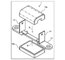
- FIG. 2 is an exploded perspective view of the noise filter according to the first embodiment.
- FIG. 3 is a perspective view illustrating a method of assembling the noise filter according to the first embodiment. It is a perspective view of the state where the noise filter of 1st Embodiment was assembled. It is a perspective view of the state where the noise filter of a 1st embodiment was molded. It is a perspective view (the 1) explaining a procedure of attaching a mounting board to a noise filter of a 1st embodiment.
- FIG. 9 is a perspective view (part 2) for explaining the procedure for attaching the mounting board to the noise filter of the first embodiment.
- FIG. 9 is a perspective view (part 2) for explaining the procedure for attaching the mounting board to the noise filter of the first embodiment.
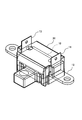
- It is an exploded perspective view of a noise filter of a 2nd embodiment.
- FIG. 9 is a perspective view illustrating an assembled state of a noise filter according to a second embodiment. It is a perspective view of the molded state of the noise filter of a 2nd embodiment. It is an exploded perspective view of a noise filter of other embodiments.
- FIG. 1 is a circuit diagram showing an example of an output noise reduction device using the noise filter 1 of the first embodiment according to the present invention.
- the noise filter module shown in FIG. 1 includes a mounting board 7 on which a capacitor and the like are mounted and the noise filter 1, and is connected between the output terminal VX and the output terminal VO of the switching power supply 5.
- the switching power supply 5 and the noise filter module are housed in a metal casing 3 made of aluminum die cast or the like.
- FIG. 1 illustrates the electrical operation and effect of the noise filter module.
- the switching power supply 5 is, for example, a power supply for a vehicle. This is a step-down switching power supply that steps down a voltage value from a main battery (not shown) that supplies a power supply voltage VIN of a drive system in a hybrid vehicle or an electric vehicle and supplies power to an auxiliary battery (not shown).
- the auxiliary battery supplies a power supply voltage to in-vehicle electrical devices such as audio devices, air conditioners, and lighting devices.
- the switching power supply 5 obtains an output of a predetermined voltage by turning on / off a power transistor (not shown) at a predetermined switching frequency f.
- a voltage fluctuates alternately between a high voltage and a low voltage at the switching frequency f.
- a current corresponding to the load current alternately intermittently flows between the power supply voltage VIN and the ground potential GND, causing a current fluctuation.
- Voltage fluctuations and current fluctuations due to the switching operation may become noise sources, causing noise to the output terminal.
- Such a noise source may propagate to the output terminal as conduction noise wrapping around via a signal path or a ground wiring, and may also propagate to the output terminal as radiation noise radiated by electromagnetic coupling such as capacitive coupling or inductive coupling.
- the radiated noise may be caused by, for example, voltage fluctuation of the internal connection. This is a case where unexpected voltage fluctuations are caused to the coupled circuit element in accordance with capacitive coupling due to a parasitic capacitance component interposed between circuit elements or between wirings. Further, it may occur with a current fluctuation of the power supply voltage VIN or the ground potential GND.
- a noise filter module is connected to the output terminal VX of the switching power supply 5.
- a choke coil L1 is provided in an output voltage path connecting an output terminal VX and an output terminal VO of the switching power supply 5, and a capacitor C1 is connected between the output terminal VX of the switching power supply 5 and the ground potential GND.
- the capacitor C2 is connected between the terminal VO and the ground potential GND.
- CLC ⁇ -type filter.
- the capacitors C1 and C2 are mounted on the component surface of the mounting board 7.
- the surface opposite to the component surface of the mounting substrate 7 is, for example, a ground surface, and is connected to the ground potential GND.
- the noise filter module can suppress noise of the switching frequency f or its harmonic frequency, which propagates in the signal path, out of the conducted noise.
- the switching frequency f in the switching power supply 5 is determined according to the power rating to be output, the specifications and ratings of each component, and the like. For example, an in-vehicle switching power supply may operate at several hundred kHz. For this reason, the switching frequency f and its harmonic frequency may overlap the frequency band of the in-vehicle AM radio, and the provision of the noise filter module makes it possible to suppress the conducted noise propagating in the signal path in these bands. .
- the switching power supply 5 and the noise filter module are housed in a metal housing 3 made of aluminum die cast or the like. Thereby, since the metal housing 3 has an electromagnetic shielding effect, propagation of radiation noise generated by the switching operation in the metal housing 3 to the output terminal VO is suppressed.
- the ground surface of the mounting board 7 is connected to the ground potential GND, the ground surface has an electromagnetic shielding effect. Is suppressed from propagating to the capacitors C1 and C2 mounted on the first and second capacitors. As a result, the performance of the noise filter module as a filter can be sufficiently exhibited.
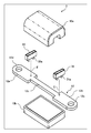
- FIG. 2 is an exploded perspective view of the noise filter 1.
- FIG. 3A is a perspective view of a method of assembling the noise filter 1
- FIG. 4 is a perspective view showing a state where the noise filter 1 is molded.
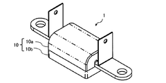
- the noise filter 1 includes a conductive bar 12, a magnetic core 10 including a magnetic core upper portion 10a and a magnetic core lower portion 10b, a lead member 13, and a lead member 14.
- the conductive bar 12 is used as an output voltage path connecting the output terminal VX and the output terminal VO of the switching power supply 5 shown in FIG.
- the conductive bar 12 has a generally flat shape, has a horizontally long shape extending in the direction of the output terminal VX and the output terminal VO of the switching power supply 5, and is formed of a metal material such as copper or carbon steel.
- Bolt portions 12a and 12b are formed at both outer ends in the extension direction with the central portion 12c interposed therebetween.
- One bolt portion 12a is provided with a bolt hole 12d for connection to the output terminal VX of the switching power supply 5, and the other bolt portion 12b is provided with a bolt hole 12e for connection to the output terminal VO.
- the bolt portion 12a is connected to the output terminal VX of the switching power supply 5 using the bolt hole 12d.
- the bolt portion 12b is an output terminal VO, and is connected to a subsequent electronic device or the like using the bolt hole 12e.
- the bolt portions 12a and 12b and the central portion 12c are arranged in the same straight line, and the conductive bar 12 is formed of a single metal member.
- the central portion 12c is slightly narrower in the width direction than the bolt portions 12a and 12b, and a magnetic core 10 composed of a magnetic core upper portion 10a and a magnetic core lower portion 10b is provided at the center of the central portion 12c. And is arranged so as to penetrate.
- the magnetic core 10 is composed of a magnetic core upper part 10a provided with a U-shaped groove 10c at the center of the lower surface in the shape of a bottom and a substantially rectangular magnetic core lower part 10b, and a magnetic material such as ferrite, for example. It is formed with.
- the magnetic core upper part 10a and the magnetic core lower part 10b are aligned as shown in FIG. 3B, so that the U-shaped groove 10c of the magnetic core upper part 10a forms a hollow part, and the conductive bar is formed in the formed hollow part. 12 penetrates, and the choke coil L1 is configured by arranging the inner side surface of the hollow portion and the central portion 12c of the conductive bar 12 so as to face each other.
- a gap (referred to as a slit) may be provided without contacting one of the left and right surfaces with respect to the conductive bar 12 with which the magnetic core upper part 10a and the magnetic core lower part 10b abut.
- a so-called core gap is formed in which a part of the path circulating in the circumferential direction with respect to the central portion 12c of the conductive bar 12 is discontinuous, and a magnetic gap composed of the magnetic core upper portion 10a and the magnetic core lower portion 10b is formed.
- the magnetic resistance in the body core 10 can be adjusted to prevent the occurrence of magnetic saturation.
- the width of the slit the magnetic resistance can be adjusted to suppress magnetic saturation, and the inductance of the choke coil L1 required for removing noise components can be secured.
- the extending direction of the conductive bar 12 corresponds to the penetrating direction penetrating the magnetic core.
- the lead members 13 and 14 are for connecting the mounting board 7 shown in FIG. 1, and are formed of a conductive metal material such as copper, nickel, or iron. As shown in FIG. 2, the lead members 13 and 14 are plate-shaped, and extend 13b and 14b extending substantially perpendicularly to the conductive bar 12 toward the mounting substrate 7, and 13a and 14a bent substantially horizontally. Is formed from. The widths 13a and 14a of the lead members 13 and 14 are substantially the same as or slightly smaller than the width of the central portion 12c of the conductive bar 12.
- the hollow portion (the U-shaped groove 10c) of the magnetic core 10 formed by combining the upper body portion 10a and the lower magnetic core portion 10b can be penetrated without interference and assembled. Further, bolt holes 13c and 14c for connecting a mounting board 7 described later are provided above the lead members 13 and 14 at 13b and 14b.
- 13a and 14a of the lead members 13 and 14 are connected to the conductive bar 12.
- the connection may be made by welding or by soldering. Alternatively, the connection may be made using a screw (not shown). Then, as shown by arrow B in FIG. 3A, the conductive bar 12 connecting the lead members 13 and 14 is sandwiched between the magnetic core upper part 10a and the magnetic core lower part 10b, and as shown in FIG. Is assembled.
- the assembled noise filter 1 is molded by a mold 20 formed of a resin material, as shown in FIG.
- a mold 20 formed of a resin material, as shown in FIG.
- most of the lead members 13 and 14 are covered with the resin by molding up to the portion excluding the upper end portions of the lead members 13 and 14 by the mold 20. Therefore, it is possible to prevent the lead members 13 and 14 from being corroded by contact with the atmosphere.
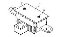
- FIG. 5A to 6B are perspective views for explaining a procedure for attaching the mounting substrate 7 to the noise filter 1.
- FIG. 5A to 6B are perspective views for explaining a procedure for attaching the mounting substrate 7 to the noise filter 1.
- concave portions 20a and 20b are provided on the upper surface of the mold 20.
- the recesses 20a and 20b have a width and depth such that the nut screws 21 and 21 are housed therein and the nut screws 21 and 21 cannot move within the recesses 20a and 20b.
- the upper ends of the lead members 13 and 14 are bent in the directions shown by arrows D and D. .
- FIG. 5B shows a state where the upper ends of the lead members 13 and 14 are bent.
- FIG. 6A after mounting screws 22, 22 are inserted into two mounting holes 7 a, 7 a provided in mounting substrate 7, inserted into bolt holes 13 c and 14 c of lead members 13 and 14, and As shown in FIG. 6B, the mounting board 7 is screwed with the screws 22 and 22 and fitted to the noise filter 1 by fitting with the nut screws 21 and 21 in the recesses 20a and 20b.
- a pattern for connecting a capacitor or the like mounted on the mounting board 7 is formed around the mounting holes 7a, 7a of the mounting board 7 in contact with the lead members 13 and 14.
- the conductive bar 12 and the mounting board 7 can be connected by the shortest lead members 13 and 14, the parasitic capacitance and the parasitic inductance of the lead members 13 and 14 can be suppressed low. . Thereby, characteristics as a noise filter module can be improved. Further, by connecting the lead members 13 and 14 to the conductive bar 12 first, the lead assembling step can be facilitated. Therefore, component costs and manufacturing costs can be reduced. In addition, since the mold 20 can be formed in a relatively simple shape, the size and shape of the mounting substrate 7 are less likely to be restricted, and it becomes possible to mount a capacitor according to the customer's request. It is possible to provide a noise filter module that can flexibly respond to the noise filter module. Also, since the lead members 13 and 14 can be integrally formed, the connection between the conductive bar 12 and the lead members 13 and 14 has improved resistance to vibration and impact, and also has improved reliability as a noise filter module. can do.
- FIG. 7 is an exploded perspective view of the noise filter 2 according to the second embodiment.
- FIG. 8A is a perspective view showing an assembled state of the noise filter 2
- FIG. 8B is a perspective view showing a state in which the noise filter 2 is molded.
- connectors 30 and 31 are employed instead of the lead members 13 and 14 described above.
- a mold formed of a resin material as shown in FIG. 8B. Molded at 40.
- four circular concave portions 40a for attaching a mounting board (not shown) are provided.
- four recesses 40a are provided, but it is sufficient that the number of recesses 40a is two or more, and the number is not limited.
- a connector having a polarity opposite to that of the connector 30 and the connector 31 is mounted on the lower surface side of the mounting board.
- the mounting board is connected to the connector 30 and the connector 31 by a connector and attached to the mold 40 by screwing or the like. If the mounting board can be held only by connector connection, screwing is not necessary. In this case, mounting and dismounting of the mounting board becomes easy, and the assembling work becomes easy.
- the switching power supply 5 is an example of an electronic device
- the noise filters 1 and 2 are an example of an output noise reduction device
- the conductive bar 12 is an example of a conductive bar
- the magnetic core 10 is an example of a magnetic core.
- the mounting substrate 7 is an example of a mounting substrate
- the lead members 13 and 14 and the connectors 30 and 31 are examples of a lead member
- the molds 20 and 40 are examples of a molding member.
- the noise filter module is a CLC ( ⁇ -type) noise filter, but an LC-type (L-type) noise filter may be employed depending on conduction noise propagating through a signal path.
- the mounting board 7 is attached with the nut screws 21, 21, but the bolt holes 13 c and 14 c of the lead members 13 and 14 are machined into female screws that fit into the male screws of the screws 22, so that the nut screws 21 are formed. 21 and 21 can be made unnecessary.
- the lead member is not limited to the above-described embodiment, and a bar-shaped lead pin 50 made of a conductive material may be used for the conductive bar 12 as shown in FIG.
- a bar-shaped lead pin 50 made of a conductive material may be used for the conductive bar 12 as shown in FIG.
- the mounting board is provided with a hole through the lead pin 50 and the mounting board and the conductive bar 12 are connected by direct soldering or the like, the component cost can be further reduced.
Abstract
This output noise reduction device according to an aspect of the present invention is configured from a conductive bar 12, a magnetic core 10 through which the conductive bar 12 penetrates, and lead members 13 and 14 that connect the conductive bar 12 and a mounting substrate 7, wherein, after the lead members 13 and 14 are connected to the conductive bar 12, the output noise reduction device is molded with a mold 20. As a result, the number of components is reduced and the occupied area of the mounting substrate is used efficiently, whereby component costs and manufacturing costs are lowered and the present invention can be applied to a wide range of customer demands.
Description
本願に開示の技術は、出力信号に混入するノイズを抑制する出力ノイズ低減装置に関し、特に、出力信号の信号経路に挿入されるインダクタンス素子を含むノイズ低減装置に関するものである。
The technology disclosed in the present application relates to an output noise reduction device that suppresses noise mixed into an output signal, and more particularly to a noise reduction device including an inductance element inserted into a signal path of an output signal.
従来より、導電バーが磁性体コアを貫通して構成されるチョークコイルと、コンデンサなどが実装される実装基板とで構成するノイズフィルタモジュールが、例えば、特許文献1などに開示されている。
Conventionally, for example, Patent Document 1 discloses a noise filter module including a choke coil in which a conductive bar penetrates a magnetic core and a mounting substrate on which a capacitor and the like are mounted.
特許文献1に開示されているノイズフィルタモジュールは、導電バーに磁性体コアが貫通されて配置し樹脂材料でモールドした汎用モジュールに、汎用モジュールの外装に沿って複数のリード部材が配置され、この複数のリード部材により、コンデンサなどが実装された実装基板が導電バーの両端部の入力端と出力端とに接続されるとともに、実装基板のGND面を接地電位GNDに接続するようになっている。
In the noise filter module disclosed in Patent Document 1, a plurality of lead members are arranged along the exterior of a general-purpose module on a general-purpose module in which a magnetic core is penetrated by a conductive bar and molded with a resin material. A plurality of lead members connect a mounting board on which a capacitor or the like is mounted to input and output ends of both ends of the conductive bar, and connect a GND surface of the mounting board to a ground potential GND. .
特許文献1に記載されたノイズフィルタモジュールでは、樹脂材料でモールドした汎用モジュールに、汎用モジュールの外装に沿って複数のリード部材が配置されているため、リード部材が大気に曝されて腐食されやすいという問題があった。また、汎用モジュールの外装に沿ってリード部材を配置するため、リード部材の形状が複雑になり、部品コストが高くなるとともにリード組付け工程が困難になるため製造コストも高くなってしまうという問題があった。また、振動や衝撃により、リード部材の接続部に接続不良が生じて、ノイズフィルタモジュールとしての信頼性も低下してしまう恐れがあった。
In the noise filter module described in Patent Literature 1, a plurality of lead members are arranged along the exterior of the general-purpose module in a general-purpose module molded with a resin material, so that the lead members are easily exposed to the atmosphere and corroded. There was a problem. Further, since the lead members are arranged along the exterior of the general-purpose module, the shape of the lead members becomes complicated, and the parts cost increases, and the lead assembling process becomes difficult, so that the production cost increases. there were. In addition, due to vibration or impact, a connection failure may occur in the connection portion of the lead member, and the reliability as a noise filter module may be reduced.
本願に開示される技術は、上記の課題に鑑み提案されたものであって、リードの組付けを改善するとともに実装基板の占有面積を効率に利用することで、部品コストや製造コストを低減するとともに、顧客の幅広い要望に対応可能な出力ノイズ低減装置を提供することを目的とする。
The technology disclosed in the present application has been proposed in view of the above problem, and reduces component costs and manufacturing costs by improving the assembling of leads and efficiently using the occupied area of the mounting board. It is another object of the present invention to provide an output noise reduction device capable of responding to a wide range of customer requests.
前記目的を達成するため請求項1に係る出力ノイズ低減装置は、実装基板を接続して電子機器からの出力信号に混入するノイズを低減する出力ノイズ低減装置であって、導電性材料により形成され、一方の端部を電子機器に係る出力端に接続する接続端子とし、他方の端部を出力端子とする導電バーと、磁性材料により形成され、導電バーが貫通する貫通孔を有する磁性体コアと、実装基板を接続端子および出力端子に接続するための導電性部材により形成した第1のリード部材および第2のリード部材とを備え、導電バーの磁性体コアと接続端子との間に第1のリード部材を、導電バーの磁性体コアと出力端子との間に第2のリード部材を、それぞれ接続した状態で、接続端子および出力端子を除く導電バーと、実装基板に接続する端部を除く第1のリード部材および第2のリード部材と、磁性体コアが、樹脂材料により形成されるモールド部材によりモールドされることを特徴とする。
In order to achieve the above object, an output noise reduction device according to claim 1 is an output noise reduction device that connects a mounting board to reduce noise mixed in an output signal from an electronic device, and is formed of a conductive material. A conductive bar having one end serving as a connection terminal for connecting to an output end of the electronic device and the other end serving as an output terminal; and a magnetic core formed of a magnetic material and having a through hole through which the conductive bar passes. And a first lead member and a second lead member formed of a conductive member for connecting the mounting board to the connection terminal and the output terminal, wherein a first lead member and a second lead member are formed between the magnetic core of the conductive bar and the connection terminal. A first lead member, a second lead member connected between the magnetic core of the conductive bar and the output terminal, and a conductive bar excluding the connection terminal and the output terminal; The first lead member and the second lead member, the magnetic core except that, characterized in that it is molded by a mold member formed of a resin material.
請求項2に係る出力ノイズ低減装置は、請求項1に記載の出力ノイズ低減装置において、第1のリード部材および第2のリード部材は、実装基板に向かって導電バーに対して略垂直方向に伸長するとともに、導電バーに接続する端部が略水平方向に屈曲して形成されており、第1のリード部材および第2のリード部材の屈曲した端部が磁性体コアの貫通孔内に位置して導電バーに接続されることを特徴とする。
An output noise reduction device according to a second aspect is the output noise reduction device according to the first aspect, wherein the first lead member and the second lead member are substantially perpendicular to the conductive bar toward the mounting substrate. The end connected to the conductive bar extends and is bent in a substantially horizontal direction, and the bent ends of the first lead member and the second lead member are located in the through holes of the magnetic core. And connected to the conductive bar.
請求項3に係る出力ノイズ低減装置は、請求項1または2に記載の出力ノイズ低減装置において、第1のリード部材および第2のリード部材は、実装基板に接続されるコネクタであることを特徴とする。
An output noise reduction device according to a third aspect is the output noise reduction device according to the first or second aspect, wherein the first lead member and the second lead member are connectors connected to a mounting board. And
請求項1に係る出力ノイズ低減装置では、第1のリード部材および第2のリード部材を導電バーに接続した状態でモールド部材によりモールドするため、例えば、第1のリード部材および第2のリード部材の上端部を除く部分までモールドして第1のリード部材および第2のリード部材の大部分が樹脂で覆うことができる。これにより、第1のリード部材および第2のリード部材は、大気に触れることを防止して、腐食を抑止することができる。また、先に第1のリード部材および第2のリード部材を導電バーに接続することにより、リード組付け工程を容易化できることから、製造コストを低減することができる。また、第1のリード部材および第2のリード部材を含めて一体成形することができることから、導電バーと第1のリード部材および第2のリード部材との接続部において振動や衝撃に対する耐性も向上し、ノイズフィルタモジュールとしての信頼性も向上することができる。
In the output noise reduction device according to claim 1, since the first lead member and the second lead member are molded by the mold member while being connected to the conductive bar, for example, the first lead member and the second lead member Most of the first lead member and the second lead member can be covered with resin by molding up to the portion excluding the upper end of the first lead member. Thus, the first lead member and the second lead member can be prevented from being exposed to the atmosphere, and the corrosion can be suppressed. In addition, by connecting the first lead member and the second lead member to the conductive bar first, the lead assembling step can be simplified, so that the manufacturing cost can be reduced. In addition, since the first lead member and the second lead member can be integrally formed, the resistance to vibration and shock at the connection between the conductive bar and the first lead member and the second lead member is also improved. In addition, the reliability of the noise filter module can be improved.
請求項2に係る出力ノイズ低減装置では、第1のリード部材および第2のリード部材は、導電バーに接続する端部が水平方向に屈曲しており、それぞれ、他方の端部が導電バーに対して略垂直方向に実装基板に接続することから、導電バーと実装基板とを接続する第1のリード部材と第2のリード部材を最短にすることができる。これにより、第1のリード部材および第2のリード部材の寄生容量や寄生インダクタンスを低く抑えることができ、ノイズフィルタモジュールとしての特性を向上させることができる。また、第1のリード部材および第2のリード部材が磁性体コア側に対向して導電バーに接続されることから、第1のリード部材および第2のリード部材に関係なく導電バーの接続端子や出力端子を設けることができる。
In the output noise reducing device according to claim 2, the first lead member and the second lead member have ends connected to the conductive bar bent in the horizontal direction, and the other ends of the first lead member and the second lead member are connected to the conductive bar. The connection between the conductive bar and the mounting board can be minimized by connecting the conductive bar and the mounting board with each other in the direction substantially perpendicular to the mounting board. Thereby, the parasitic capacitance and the parasitic inductance of the first lead member and the second lead member can be suppressed low, and the characteristics as a noise filter module can be improved. Further, since the first lead member and the second lead member are connected to the conductive bar so as to face the magnetic core side, the connection terminal of the conductive bar is independent of the first lead member and the second lead member. And an output terminal.
請求項3に係る出力ノイズ低減装置では、導電バーと実装基板とがコネクタ接続することから、容易に、実装基板の取り付けや取り外しができる。また、コネクタ接続だけで実装基板が保持可能であれば、実装基板を取り付けるためのネジ留めなどが不要となり、部品数の低減や組み付け作業の削減が可能になり、結果、製造コストを低減できる。
According to the third aspect of the present invention, since the conductive bar and the mounting board are connected by a connector, the mounting board can be easily attached or detached. In addition, if the mounting board can be held only by connecting the connector, screwing or the like for mounting the mounting board becomes unnecessary, so that the number of parts and the assembling work can be reduced, and as a result, the manufacturing cost can be reduced.
図1は本願に係る第1実施形態のノイズフィルタ1を用いた出力ノイズ低減装置の一例を示す回路図である。図1に示すノイズフィルタモジュールは、コンデンサなどが実装された実装基板7とノイズフィルタ1とから構成され、スイッチング電源5の出力端子VXと出力端子VOとの間に接続される。スイッチング電源5、ノイズフィルタモジュールは、アルミダイカスト製などの金属筐体3に収納されている。図1においては、ノイズフィルタモジュールに関する電気的な作用効果を説明する。
FIG. 1 is a circuit diagram showing an example of an output noise reduction device using the noise filter 1 of the first embodiment according to the present invention. The noise filter module shown in FIG. 1 includes a mounting board 7 on which a capacitor and the like are mounted and the noise filter 1, and is connected between the output terminal VX and the output terminal VO of the switching power supply 5. The switching power supply 5 and the noise filter module are housed in a metal casing 3 made of aluminum die cast or the like. FIG. 1 illustrates the electrical operation and effect of the noise filter module.
スイッチング電源5は、例えば、車載用の電源である。ハイブリッド車あるいは電気自動車等における駆動系の電源電圧VINを供給するメインバッテリー(不図示)から電圧値を降圧して補機バッテリー(不図示)への電力供給を行う降圧型のスイッチング電源である。補機バッテリーは、オーディオ機器、エアコン機器、照明機器などの車内電装機器に電源電圧を供給する。
The switching power supply 5 is, for example, a power supply for a vehicle. This is a step-down switching power supply that steps down a voltage value from a main battery (not shown) that supplies a power supply voltage VIN of a drive system in a hybrid vehicle or an electric vehicle and supplies power to an auxiliary battery (not shown). The auxiliary battery supplies a power supply voltage to in-vehicle electrical devices such as audio devices, air conditioners, and lighting devices.
スイッチング電源5は、パワートランジスタ(不図示)を所定スイッチング周波数fでオンオフ制御させることで所定電圧の出力を得る。スイッチング電源5では、このスイッチング動作に応じて、内部結線によってはスイッチング周波数fで高電圧と低電圧との間で交互に電圧変動が生ずる。また、負荷電流に応じた電流が電源電圧VINおよび接地電位GNDに交互に断続して流れ電流変動が生ずる。スイッチング動作による電圧変動と電流変動とがノイズ源となり出力端子へのノイズを招来する場合がある。
The switching power supply 5 obtains an output of a predetermined voltage by turning on / off a power transistor (not shown) at a predetermined switching frequency f. In the switching power supply 5, in accordance with this switching operation, depending on the internal connection, a voltage fluctuates alternately between a high voltage and a low voltage at the switching frequency f. Further, a current corresponding to the load current alternately intermittently flows between the power supply voltage VIN and the ground potential GND, causing a current fluctuation. Voltage fluctuations and current fluctuations due to the switching operation may become noise sources, causing noise to the output terminal.
こうしたノイズ源は、信号経路や接地配線を介して回り込む伝導ノイズとして出力端子に伝搬する他、容量結合や誘導結合などの電磁的結合により放射される放射ノイズとして出力端子に伝搬するおそれがある。ここで、放射ノイズとしては、例えば、内部結線の電圧変動に伴って生ずる場合がある。回路要素間や配線間等に介在する寄生の容量成分による容量結合に応じて結合先の回路要素に対して不測の電圧変動を招来する場合である。また、電源電圧VINや接地電位GNDの電流変動に伴って生ずる場合がある。配線される電源電圧VINや接地電位GNDの配線経路に介在する寄生の誘導成分による逆起電力に応じて電源電圧VINや接地電位GNDに不測の電圧変動を招来する場合である。
Such a noise source may propagate to the output terminal as conduction noise wrapping around via a signal path or a ground wiring, and may also propagate to the output terminal as radiation noise radiated by electromagnetic coupling such as capacitive coupling or inductive coupling. Here, the radiated noise may be caused by, for example, voltage fluctuation of the internal connection. This is a case where unexpected voltage fluctuations are caused to the coupled circuit element in accordance with capacitive coupling due to a parasitic capacitance component interposed between circuit elements or between wirings. Further, it may occur with a current fluctuation of the power supply voltage VIN or the ground potential GND. This is a case where unexpected voltage fluctuations are caused in the power supply voltage VIN or the ground potential GND according to the back electromotive force due to a parasitic induction component interposed in the wiring path of the power supply voltage VIN or the ground potential GND to be wired.
スイッチング電源5の出力端子VXにはノイズフィルタモジュールが接続されている。ノイズフィルタモジュールは、スイッチング電源5の出力端子VXと出力端子VOとを結ぶ出力電圧経路にチョークコイルL1が設けられ、スイッチング電源5の出力端子VXと接地電位GNDとの間にコンデンサC1が、出力端子VOと接地電位GNDとの間にコンデンサC2が接続される構造を有している。いわゆるCLC型(π型)フィルタの構成である。コンデンサC1およびコンデンサC2は実装基板7の部品面に実装される。実装基板7の部品面の反対面は、例えば、グランド面となっており、接地電位GNDに接続されている。コンデンサC1およびコンデンサC2の各々の一端はグランド面に接続されて接地電位GNDに接続される。ノイズフィルタモジュールにより、伝導ノイズのうち信号経路を伝搬するスイッチング周波数fやその高調波周波数のノイズは抑制することができる。ここで、スイッチング電源5におけるスイッチング周波数fは、出力される電力定格や各構成素子の仕様や定格などに応じて定められる。例えば、車載用のスイッチング電源では数100kHzで動作することが考えられる。このため、スイッチング周波数fやその高調波周波数が、車載AMラジオの周波数帯域に重なる場合があり、ノイズフィルタモジュールを備えることにより、これらの帯域で信号経路を伝搬する伝導ノイズを抑制することができる。
ノ イ ズ A noise filter module is connected to the output terminal VX of the switching power supply 5. In the noise filter module, a choke coil L1 is provided in an output voltage path connecting an output terminal VX and an output terminal VO of the switching power supply 5, and a capacitor C1 is connected between the output terminal VX of the switching power supply 5 and the ground potential GND. The capacitor C2 is connected between the terminal VO and the ground potential GND. This is a configuration of a so-called CLC (π-type) filter. The capacitors C1 and C2 are mounted on the component surface of the mounting board 7. The surface opposite to the component surface of the mounting substrate 7 is, for example, a ground surface, and is connected to the ground potential GND. One end of each of the capacitor C1 and the capacitor C2 is connected to the ground plane, and is connected to the ground potential GND. The noise filter module can suppress noise of the switching frequency f or its harmonic frequency, which propagates in the signal path, out of the conducted noise. Here, the switching frequency f in the switching power supply 5 is determined according to the power rating to be output, the specifications and ratings of each component, and the like. For example, an in-vehicle switching power supply may operate at several hundred kHz. For this reason, the switching frequency f and its harmonic frequency may overlap the frequency band of the in-vehicle AM radio, and the provision of the noise filter module makes it possible to suppress the conducted noise propagating in the signal path in these bands. .
また、スイッチング電源5およびノイズフィルタモジュールは、アルミダイカスト製などの金属筐体3に収納されている。これにより、金属筐体3が電磁的なシールドの効果を奏するため、金属筐体3内でのスイッチング動作により発生する放射ノイズが出力端子VOに伝搬することが抑制される。
(4) The switching power supply 5 and the noise filter module are housed in a metal housing 3 made of aluminum die cast or the like. Thereby, since the metal housing 3 has an electromagnetic shielding effect, propagation of radiation noise generated by the switching operation in the metal housing 3 to the output terminal VO is suppressed.
さらに、実装基板7のグランド面が接地電位GNDに接続されていることから、グランド面が電磁的なシールドの効果を奏するため、金属筐体3内でのスイッチング動作により発生する放射ノイズが部品面に実装されたコンデンサC1およびコンデンサC2に伝搬することが抑制される。これにより、ノイズフィルタモジュールのフィルタとしての性能が十分発揮することができるのである。
Further, since the ground surface of the mounting board 7 is connected to the ground potential GND, the ground surface has an electromagnetic shielding effect. Is suppressed from propagating to the capacitors C1 and C2 mounted on the first and second capacitors. As a result, the performance of the noise filter module as a filter can be sufficiently exhibited.
次に、本願に係る第1実施形態のノイズフィルタ1の形状・構造に関して説明する。図2はノイズフィルタ1の分解斜視図である。図3Aはノイズフィルタ1の組み付け方法、図3Bはノイズフィルタ1の組み付けされた状態の斜視図である。そして、図4はノイズフィルタ1がモールドされた状態の斜視図である。
Next, the shape and structure of the noise filter 1 according to the first embodiment of the present invention will be described. FIG. 2 is an exploded perspective view of the noise filter 1. FIG. 3A is a perspective view of a method of assembling the noise filter 1, and FIG. FIG. 4 is a perspective view showing a state where the noise filter 1 is molded.
図2に示すように、ノイズフィルタ1は、導電バー12、磁性体コア上部10aと磁性体コア下部10bとからなる磁性体コア10、リード部材13およびリード部材14から構成されている。
As shown in FIG. 2, the noise filter 1 includes a conductive bar 12, a magnetic core 10 including a magnetic core upper portion 10a and a magnetic core lower portion 10b, a lead member 13, and a lead member 14.
導電バー12は、図1に示すスイッチング電源5の出力端子VXと出力端子VOとをつなぐ出力電圧経路として用いられる。導電バー12は、概ね平板状で、スイッチング電源5の出力端子VXと出力端子VOの方向に伸長する横長形状を有し、例えば銅や炭素鋼等の金属材料で形成されている。中央部12cを挟んで伸長方向の外側の両端部にボルト部12a、12bが形成されている。一方のボルト部12aには、スイッチング電源5の出力端子VXに接続するためのボルト穴12dが、他方のボルト部12bには、出力端子VOに接続するためのボルト穴12eが設けられている。すなわち、ボルト穴12dを用いてボルト部12aはスイッチング電源5の出力端子VXに接続される。また、ボルト部12bは出力端子VOであり、ボルト穴12eを用いて後段の電子機器等に接続される。ボルト部12a、12bおよび中央部12cは同一直線状に配置されており、導電バー12は単一の金属部材で形成されている。中央部12cはボルト部12a、12bより幅方向にやや狭くなっており、中央部12cの中心には磁性体コア上部10aと磁性体コア下部10bとから構成される磁性体コア10が導電バー12により貫通されて配置されている。
The conductive bar 12 is used as an output voltage path connecting the output terminal VX and the output terminal VO of the switching power supply 5 shown in FIG. The conductive bar 12 has a generally flat shape, has a horizontally long shape extending in the direction of the output terminal VX and the output terminal VO of the switching power supply 5, and is formed of a metal material such as copper or carbon steel. Bolt portions 12a and 12b are formed at both outer ends in the extension direction with the central portion 12c interposed therebetween. One bolt portion 12a is provided with a bolt hole 12d for connection to the output terminal VX of the switching power supply 5, and the other bolt portion 12b is provided with a bolt hole 12e for connection to the output terminal VO. That is, the bolt portion 12a is connected to the output terminal VX of the switching power supply 5 using the bolt hole 12d. The bolt portion 12b is an output terminal VO, and is connected to a subsequent electronic device or the like using the bolt hole 12e. The bolt portions 12a and 12b and the central portion 12c are arranged in the same straight line, and the conductive bar 12 is formed of a single metal member. The central portion 12c is slightly narrower in the width direction than the bolt portions 12a and 12b, and a magnetic core 10 composed of a magnetic core upper portion 10a and a magnetic core lower portion 10b is provided at the center of the central portion 12c. And is arranged so as to penetrate.
磁性体コア10は、かまぼこ形状で下面中央部にコの字状溝10cを設けた磁性体コア上部10aと略長方体状の磁性体コア下部10bとから構成され、例えばフェライト等の磁性材料で形成されている。磁性体コア上部10aと磁性体コア下部10bとが図3Bに示すように合わせることにより、磁性体コア上部10aのコの字状溝10cが中空部を形成し、形成された中空部に導電バー12が貫通し、中空部の内側面と導電バー12の中央部12cとを対向させて配置することにより、チョークコイルL1が構成される。尚、磁性体コア上部10aと磁性体コア下部10bとが当接する導電バー12に対して左右の面の内、一方については当接せず隙間(スリットと言う)を設けてもよい。これにより、導電バー12の中央部12cに対して周方向に周回する経路の一部が不連続となる、いわゆるコアギャップを形成し、磁性体コア上部10aと磁性体コア下部10bとからなる磁性体コア10における磁気抵抗を調整して磁気飽和の発生を防止することができる。スリットの幅を調整することにより、磁気抵抗を調整して磁気飽和を抑制し、ノイズ成分の除去に必要なチョークコイルL1のインダクタンスを確保することができる。
The magnetic core 10 is composed of a magnetic core upper part 10a provided with a U-shaped groove 10c at the center of the lower surface in the shape of a bottom and a substantially rectangular magnetic core lower part 10b, and a magnetic material such as ferrite, for example. It is formed with. The magnetic core upper part 10a and the magnetic core lower part 10b are aligned as shown in FIG. 3B, so that the U-shaped groove 10c of the magnetic core upper part 10a forms a hollow part, and the conductive bar is formed in the formed hollow part. 12 penetrates, and the choke coil L1 is configured by arranging the inner side surface of the hollow portion and the central portion 12c of the conductive bar 12 so as to face each other. Note that a gap (referred to as a slit) may be provided without contacting one of the left and right surfaces with respect to the conductive bar 12 with which the magnetic core upper part 10a and the magnetic core lower part 10b abut. As a result, a so-called core gap is formed in which a part of the path circulating in the circumferential direction with respect to the central portion 12c of the conductive bar 12 is discontinuous, and a magnetic gap composed of the magnetic core upper portion 10a and the magnetic core lower portion 10b is formed. The magnetic resistance in the body core 10 can be adjusted to prevent the occurrence of magnetic saturation. By adjusting the width of the slit, the magnetic resistance can be adjusted to suppress magnetic saturation, and the inductance of the choke coil L1 required for removing noise components can be secured.
ここで、導電バー12の伸長方向は、磁性体コアを貫通する貫通方向に相当する。
伸長 Here, the extending direction of the conductive bar 12 corresponds to the penetrating direction penetrating the magnetic core.
リード部材13および14は、図1にした実装基板7を接続するためのものであり、例えば銅、ニッケル、あるいは鉄等の導電性の金属材料で形成されている。リード部材13および14は、図2に示すように、板状であり、実装基板7に向かって導電バー12に対して略垂直方向に伸びる13bおよび14bと略水平方向に屈曲した13aおよび14aとから形成されている。そして、リード部材13および14の13aおよび14aは、導電バー12の中央部12cの幅と略同一かまたはやや狭い幅になっており、リード部材13および14が導電バー12に接続した状態で磁性体コア上部10aと磁性体コア下部10bとが合わさって形成される磁性体コア10の中空部(コの字状溝10c)を干渉することなく貫通させて組み付けることができる。また、リード部材13および14の13bおよび14bの上部には、後述する実装基板7を接続するためのボルト穴13cおよび14cが設けられている。
The lead members 13 and 14 are for connecting the mounting board 7 shown in FIG. 1, and are formed of a conductive metal material such as copper, nickel, or iron. As shown in FIG. 2, the lead members 13 and 14 are plate-shaped, and extend 13b and 14b extending substantially perpendicularly to the conductive bar 12 toward the mounting substrate 7, and 13a and 14a bent substantially horizontally. Is formed from. The widths 13a and 14a of the lead members 13 and 14 are substantially the same as or slightly smaller than the width of the central portion 12c of the conductive bar 12. When the lead members 13 and 14 are connected to the conductive bar 12, The hollow portion (the U-shaped groove 10c) of the magnetic core 10 formed by combining the upper body portion 10a and the lower magnetic core portion 10b can be penetrated without interference and assembled. Further, bolt holes 13c and 14c for connecting a mounting board 7 described later are provided above the lead members 13 and 14 at 13b and 14b.
第1実施形態のノイズフィルタ1では、最初に、図2の矢印Aに示すように、リード部材13および14の13aおよび14aを導電バー12に接続する。接続方法としては、溶接して接続してもよいし、半田付けにて接続してもよい。また、図示しないネジを用いて接続してもよい。そして、図3Aの矢印Bに示すように、リード部材13および14を接続した導電バー12を磁性体コア上部10aと磁性体コア下部10bとで挟んで、図3Bに示すように、ノイズフィルタ1が組み付けられる。
In the noise filter 1 of the first embodiment, first, as shown by the arrow A in FIG. 2, 13a and 14a of the lead members 13 and 14 are connected to the conductive bar 12. The connection may be made by welding or by soldering. Alternatively, the connection may be made using a screw (not shown). Then, as shown by arrow B in FIG. 3A, the conductive bar 12 connecting the lead members 13 and 14 is sandwiched between the magnetic core upper part 10a and the magnetic core lower part 10b, and as shown in FIG. Is assembled.
組み付けられたノイズフィルタ1は、図4に示すように、樹脂材料により形成されるモールド20でモールドされる。図4に示すように、モールド20により、リード部材13および14の上端部を除く部分までモールドすることにより、リード部材13および14の大部分が樹脂で覆われる。そのため、大気に触れることを防止して、リード部材13および14の腐食を抑止することができる。
(4) The assembled noise filter 1 is molded by a mold 20 formed of a resin material, as shown in FIG. As shown in FIG. 4, most of the lead members 13 and 14 are covered with the resin by molding up to the portion excluding the upper end portions of the lead members 13 and 14 by the mold 20. Therefore, it is possible to prevent the lead members 13 and 14 from being corroded by contact with the atmosphere.
次に、モールドされたノイズフィルタ1に実装基板7を接続する方法を説明する。図5A~図6Bは、ノイズフィルタ1に実装基板7を取り付ける手順の説明する斜視図である。
Next, a method of connecting the mounting substrate 7 to the molded noise filter 1 will be described. 5A to 6B are perspective views for explaining a procedure for attaching the mounting substrate 7 to the noise filter 1. FIG.
図5Aに示すように、モールド20の上面には凹部20aおよび20bが設けられている。凹部20aおよび20bは、その中にナットネジ21、21が収められて凹部20aおよび20b内でナットネジ21、21が移動不可の程度の幅および深さになっている。そして、図5Aの矢印C、Cに示すように、ナットネジ21、21がモールド20の凹部20aおよび20b内に挿入した後、リード部材13および14の上端部を矢印D、Dに示す方向に折り曲げる。この時、リード部材13および14のボルト穴13cおよび14cが、凹部20aおよび20bに挿入されたナットネジ21、21のネジ穴に一致するように、予め、凹部20aおよび20bの位置が設定されている。図5Bには、リード部材13および14の上端部が折り曲げられた状態を示す。
凹 部 As shown in FIG. 5A, concave portions 20a and 20b are provided on the upper surface of the mold 20. The recesses 20a and 20b have a width and depth such that the nut screws 21 and 21 are housed therein and the nut screws 21 and 21 cannot move within the recesses 20a and 20b. Then, as shown by arrows C and C in FIG. 5A, after the nut screws 21 and 21 are inserted into the recesses 20a and 20b of the mold 20, the upper ends of the lead members 13 and 14 are bent in the directions shown by arrows D and D. . At this time, the positions of the recesses 20a and 20b are set in advance so that the bolt holes 13c and 14c of the lead members 13 and 14 match the screw holes of the nut screws 21 and 21 inserted into the recesses 20a and 20b. . FIG. 5B shows a state where the upper ends of the lead members 13 and 14 are bent.
図6Aに示すように、実装基板7に設けられた2つの取り付け穴7a、7aに取り付けネジ22、22を挿入後、リード部材13および14のボルト穴13cおよび14cに挿入して、モールド20の凹部20aおよび20b内のナットネジ21、21と嵌合させて、図6Bに示すように、実装基板7をネジ22、22によりネジ留めしてノイズフィルタ1に取り付ける。尚、実装基板7を取り付けた際に、リード部材13および14に接する実装基板7の取り付け穴7a、7aの周囲は実装基板7に実装されるコンデンサなどを接続するパターンが形成されており、実装基板7をノイズフィルタ1に取り付けることにより、例えば、図1に示すように、実装基板7に実装されたコンデンサC1やC2に接続され、上記のようなノイズフィルタモジュールとして機能する。
As shown in FIG. 6A, after mounting screws 22, 22 are inserted into two mounting holes 7 a, 7 a provided in mounting substrate 7, inserted into bolt holes 13 c and 14 c of lead members 13 and 14, and As shown in FIG. 6B, the mounting board 7 is screwed with the screws 22 and 22 and fitted to the noise filter 1 by fitting with the nut screws 21 and 21 in the recesses 20a and 20b. When the mounting board 7 is mounted, a pattern for connecting a capacitor or the like mounted on the mounting board 7 is formed around the mounting holes 7a, 7a of the mounting board 7 in contact with the lead members 13 and 14. By attaching the substrate 7 to the noise filter 1, for example, as shown in FIG. 1, it is connected to the capacitors C1 and C2 mounted on the mounting substrate 7, and functions as the above-described noise filter module.
上述のノイズフィルタ1によれば、導電バー12と実装基板7とを最短のリード部材13および14で接続することができるため、リード部材13および14の寄生容量や寄生インダクタンスを低く抑えることができる。これにより、ノイズフィルタモジュールとしての特性を向上させることができる。また、先にリード部材13および14を導電バー12に接続することにより、リード組付け工程を容易化することができる。そのため、部品コストや製造コストを低減することができる。また、モールド20を比較的単純な形状にすることができることから、実装基板7の大きさや形状が制約されにくくなり、顧客の要望に応じたコンデンサを実装することが可能になり、顧客の要望に対して柔軟に対応可能なノイズフィルタモジュールを提供することができる。また、リード部材13および14を含めて一体成形することができることから、導電バー12とリード部材13および14との接続部において振動や衝撃に対する耐性も向上し、ノイズフィルタモジュールとしての信頼性も向上することができる。
According to the above-described noise filter 1, since the conductive bar 12 and the mounting board 7 can be connected by the shortest lead members 13 and 14, the parasitic capacitance and the parasitic inductance of the lead members 13 and 14 can be suppressed low. . Thereby, characteristics as a noise filter module can be improved. Further, by connecting the lead members 13 and 14 to the conductive bar 12 first, the lead assembling step can be facilitated. Therefore, component costs and manufacturing costs can be reduced. In addition, since the mold 20 can be formed in a relatively simple shape, the size and shape of the mounting substrate 7 are less likely to be restricted, and it becomes possible to mount a capacitor according to the customer's request. It is possible to provide a noise filter module that can flexibly respond to the noise filter module. Also, since the lead members 13 and 14 can be integrally formed, the connection between the conductive bar 12 and the lead members 13 and 14 has improved resistance to vibration and impact, and also has improved reliability as a noise filter module. can do.
次に、本願に係る第2実施形態のノイズフィルタ2について説明する。図7は、第2実施形態のノイズフィルタ2の分解斜視図である。図8Aは、ノイズフィルタ2の組み付け状態を示す斜視図であり、図8Bは、ノイズフィルタ2をモールドした状態の斜視図である。
Next, the noise filter 2 according to the second embodiment of the invention will be described. FIG. 7 is an exploded perspective view of the noise filter 2 according to the second embodiment. FIG. 8A is a perspective view showing an assembled state of the noise filter 2, and FIG. 8B is a perspective view showing a state in which the noise filter 2 is molded.
ノイズフィルタ2では、上述のリード部材13および14の代わりにコネクタ30および31を採用する。図7の矢印E、Eに示すように、コネクタ30およびコネクタ31の接続ピン30aおよび31aを導電バー12に半田付けなどにより接続した後、図8Bに示すように、樹脂材料により形成されるモールド40でモールドされる。モールド40の上面には、(図示しない)実装基板を取り付けるための円形の凹部40aが4箇所設けてある。本実施形態では、凹部40aは4箇所設けてあるが、2箇所以上であればよいのであって、その数は限定するものではない。そして、実装基板の下面側には、コネクタ30およびコネクタ31とは反対極のコネクタが実装されており、実装基板をコネクタ30およびコネクタ31とコネクタ接続してモールド40にネジ留めなどにより取り付ける。コネクタ接続だけで実装基板が保持可能であれば、ネジ留めなどは必要がない。この場合、実装基板の取り付けや取り外しが容易になり、組み付け作業が容易になる。
In the noise filter 2, connectors 30 and 31 are employed instead of the lead members 13 and 14 described above. After the connection pins 30a and 31a of the connector 30 and the connector 31 are connected to the conductive bar 12 by soldering or the like as shown by arrows E and E in FIG. 7, a mold formed of a resin material as shown in FIG. 8B. Molded at 40. On the upper surface of the mold 40, four circular concave portions 40a for attaching a mounting board (not shown) are provided. In the present embodiment, four recesses 40a are provided, but it is sufficient that the number of recesses 40a is two or more, and the number is not limited. On the lower surface side of the mounting board, a connector having a polarity opposite to that of the connector 30 and the connector 31 is mounted. The mounting board is connected to the connector 30 and the connector 31 by a connector and attached to the mold 40 by screwing or the like. If the mounting board can be held only by connector connection, screwing is not necessary. In this case, mounting and dismounting of the mounting board becomes easy, and the assembling work becomes easy.
ここで、スイッチング電源5は電子機器の一例であり、ノイズフィルタ1および2は出力ノイズ低減装置の一例であり、導電バー12は導電バーの一例であり、磁性体コア10は磁性体コアの一例であり、実装基板7は実装基板の一例であり、リード部材13、14およびコネクタ30、31はリード部材の一例であり、モールド20、40はモールド部材の一例である。
Here, the switching power supply 5 is an example of an electronic device, the noise filters 1 and 2 are an example of an output noise reduction device, the conductive bar 12 is an example of a conductive bar, and the magnetic core 10 is an example of a magnetic core. The mounting substrate 7 is an example of a mounting substrate, the lead members 13 and 14 and the connectors 30 and 31 are examples of a lead member, and the molds 20 and 40 are examples of a molding member.
以上、本発明の実施形態について詳述してきたが、これらはあくまでも例示であって、本発明はかかる実施形態における具体的な記載によって、何等、限定的に解釈されるものでなく、当業者の知識に基づいて種々なる変更、修正、改良等を加えた態様において実施され得るものであり、また、そのような実施態様が、本発明の趣旨を逸脱しない限り、何れも、本発明の範囲内に含まれるものであることが、理解されるべきである。
As described above, the embodiments of the present invention have been described in detail. However, these are merely examples, and the present invention is not to be construed as being limited in any way by the specific description in the embodiments, and is not limited to those skilled in the art. Various changes, modifications, improvements, and the like can be performed based on knowledge, and any such embodiments are within the scope of the present invention unless departing from the spirit of the present invention. Should be understood to be included in
例えば、上記実施形態ではノイズフィルタモジュールはCLC型(π型)のノイズフィルタとしたが、信号経路を伝搬する伝導ノイズによっては、LC型(L型)のノイズフィルタを採用してもよい。
For example, in the above-described embodiment, the noise filter module is a CLC (π-type) noise filter, but an LC-type (L-type) noise filter may be employed depending on conduction noise propagating through a signal path.
上記第1実施形態では、ナットネジ21、21で実装基板7を取り付けたが、リード部材13および14のボルト穴13cおよび14cをネジ22の雄ネジに嵌合する雌ネジに加工することにより、ナットネジ21、21を不要にすることができる。
In the first embodiment, the mounting board 7 is attached with the nut screws 21, 21, but the bolt holes 13 c and 14 c of the lead members 13 and 14 are machined into female screws that fit into the male screws of the screws 22, so that the nut screws 21 are formed. 21 and 21 can be made unnecessary.
また、リード部材は上記実施形態に限定されるものではなく、図9に示すように、導電バー12に導電性材料で形成した棒状のリードピン50を採用してもよい。この場合、実装基板にリードピン50を貫通する穴を設け、直接半田付けなどで実装基板と導電バー12とを接続すれば、部品コストがさらに低減することができる。
The lead member is not limited to the above-described embodiment, and a bar-shaped lead pin 50 made of a conductive material may be used for the conductive bar 12 as shown in FIG. In this case, if the mounting board is provided with a hole through the lead pin 50 and the mounting board and the conductive bar 12 are connected by direct soldering or the like, the component cost can be further reduced.
本発明は上記実施の形態に制限されるものではなく、本発明の精神及び範囲から離脱することなく、様々な変更及び変形が可能である。従って、本発明の範囲を公にするために、以下の請求項を添付する。
The present invention is not limited to the above-described embodiment, and various changes and modifications can be made without departing from the spirit and scope of the present invention. Therefore, the following claims are appended to make the scope of the present invention public.
本願は、2018年6月26日提出の日本国特許出願特願2018-120478を基礎として優先権を主張するものであり、その記載内容の全てを、ここに援用する。
This application claims the priority of Japanese Patent Application No. 2018-120478 filed on June 26, 2018, the entire contents of which are incorporated herein by reference.
1、2・・ノイズフィルタ
3・・金属筐体
5・・スイッチング電源
7・・実装基板
10・・磁性体コア
12・・導電バー
13、14・・リード部材
20、40・・モールド
30、31・・コネクタ 1, 2,noise filter 3, metal housing 5, switching power supply 7, mounting substrate 10, magnetic core 12, conductive bar 13, 14, lead member 20, 40, mold 30, 31 ··connector
3・・金属筐体
5・・スイッチング電源
7・・実装基板
10・・磁性体コア
12・・導電バー
13、14・・リード部材
20、40・・モールド
30、31・・コネクタ 1, 2,
Claims (3)
- 実装基板を接続して電子機器からの出力信号に混入するノイズを低減する出力ノイズ低減装置であって、
導電性材料により形成され、一方の端部を前記電子機器に係る出力端に接続する接続端子とし、他方の端部を出力端子とする導電バーと、
磁性材料により形成され、前記導電バーが貫通する貫通孔を有する磁性体コアと、
前記実装基板を前記接続端子および前記出力端子に接続するための導電性部材により形成した第1のリード部材および第2のリード部材とを備え、
前記導電バーの前記磁性体コアと前記接続端子との間に前記第1のリード部材を、前記導電バーの前記磁性体コアと前記出力端子との間に前記第2のリード部材を、それぞれ接続した状態で、前記接続端子および前記出力端子を除く導電バーと、前記実装基板に接続する端部を除く第1のリード部材および第2のリード部材と、前記磁性体コアとが、樹脂材料により形成されるモールド部材によりモールドされることを特徴とする出力ノイズ低減装置。 An output noise reduction device that connects a mounting board and reduces noise mixed into an output signal from an electronic device,
A conductive bar formed of a conductive material, having one end serving as a connection terminal connected to an output end of the electronic device, and the other end serving as an output terminal;
A magnetic core formed of a magnetic material and having a through hole through which the conductive bar passes,
A first lead member and a second lead member formed of a conductive member for connecting the mounting board to the connection terminals and the output terminals,
The first lead member is connected between the magnetic core of the conductive bar and the connection terminal, and the second lead member is connected between the magnetic core of the conductive bar and the output terminal. In this state, the conductive bar except for the connection terminal and the output terminal, the first lead member and the second lead member except for the end connected to the mounting board, and the magnetic core are made of a resin material. An output noise reduction device characterized by being molded by a formed molding member. - 前記第1のリード部材および前記第2のリード部材は、前記実装基板に向かって前記導電バーに対して略垂直方向に伸長するとともに、前記導電バーに接続する端部が略水平方向に屈曲して形成されており、前記第1のリード部材および前記第2のリード部材の前記屈曲した端部が前記磁性体コアの前記貫通孔内に位置して前記導電バーに接続されることを特徴とする請求項1に記載の出力ノイズ低減装置。 The first lead member and the second lead member extend in a direction substantially perpendicular to the conductive bar toward the mounting board, and an end connected to the conductive bar is bent in a substantially horizontal direction. Wherein the bent ends of the first lead member and the second lead member are located in the through holes of the magnetic core and connected to the conductive bar. The output noise reduction device according to claim 1.
- 前記第1のリード部材および前記第2のリード部材は、前記実装基板に接続されるコネクタであることを特徴とする請求項1または2に記載の出力ノイズ低減装置。 3. The output noise reduction device according to claim 1, wherein the first lead member and the second lead member are connectors connected to the mounting board.
Applications Claiming Priority (2)
| Application Number | Priority Date | Filing Date | Title |
|---|---|---|---|
| JP2018120478A JP7185894B2 (en) | 2018-06-26 | 2018-06-26 | Output noise reduction device |
| JP2018-120478 | 2018-06-26 |
Publications (1)
| Publication Number | Publication Date |
|---|---|
| WO2020003698A1 true WO2020003698A1 (en) | 2020-01-02 |
Family
ID=68987030
Family Applications (1)
| Application Number | Title | Priority Date | Filing Date |
|---|---|---|---|
| PCT/JP2019/016276 WO2020003698A1 (en) | 2018-06-26 | 2019-04-16 | Output noise reduction device |
Country Status (2)
| Country | Link |
|---|---|
| JP (1) | JP7185894B2 (en) |
| WO (1) | WO2020003698A1 (en) |
Cited By (1)
| Publication number | Priority date | Publication date | Assignee | Title |
|---|---|---|---|---|
| AT524151A3 (en) * | 2020-08-26 | 2022-12-15 | Schaffner Emv Ag | Stackable noise filter |
Citations (6)
| Publication number | Priority date | Publication date | Assignee | Title |
|---|---|---|---|---|
| JPH0186715U (en) * | 1987-11-30 | 1989-06-08 | ||
| JP2006311364A (en) * | 2005-04-28 | 2006-11-09 | Tdk Corp | Three terminal electronic component |
| JP2015057806A (en) * | 2013-08-09 | 2015-03-26 | 北川工業株式会社 | Output noise reduction device |
| JP2016072505A (en) * | 2014-09-30 | 2016-05-09 | 北川工業株式会社 | Output noise reduction device |
| JP2017041400A (en) * | 2015-08-21 | 2017-02-23 | 株式会社オートネットワーク技術研究所 | Filter element built-in connector |
| JP2018019512A (en) * | 2016-07-28 | 2018-02-01 | 北川工業株式会社 | Output noise reduction device |
Family Cites Families (2)
| Publication number | Priority date | Publication date | Assignee | Title |
|---|---|---|---|---|
| JP5272191B2 (en) * | 2007-08-31 | 2013-08-28 | 三菱電機株式会社 | Semiconductor device and manufacturing method of semiconductor device |
| EP2413336A4 (en) * | 2009-03-25 | 2017-10-04 | Sumitomo Electric Industries, Ltd. | Reactor |
-
2018
- 2018-06-26 JP JP2018120478A patent/JP7185894B2/en active Active
-
2019
- 2019-04-16 WO PCT/JP2019/016276 patent/WO2020003698A1/en active Application Filing
Patent Citations (6)
| Publication number | Priority date | Publication date | Assignee | Title |
|---|---|---|---|---|
| JPH0186715U (en) * | 1987-11-30 | 1989-06-08 | ||
| JP2006311364A (en) * | 2005-04-28 | 2006-11-09 | Tdk Corp | Three terminal electronic component |
| JP2015057806A (en) * | 2013-08-09 | 2015-03-26 | 北川工業株式会社 | Output noise reduction device |
| JP2016072505A (en) * | 2014-09-30 | 2016-05-09 | 北川工業株式会社 | Output noise reduction device |
| JP2017041400A (en) * | 2015-08-21 | 2017-02-23 | 株式会社オートネットワーク技術研究所 | Filter element built-in connector |
| JP2018019512A (en) * | 2016-07-28 | 2018-02-01 | 北川工業株式会社 | Output noise reduction device |
Cited By (2)
| Publication number | Priority date | Publication date | Assignee | Title |
|---|---|---|---|---|
| AT524151A3 (en) * | 2020-08-26 | 2022-12-15 | Schaffner Emv Ag | Stackable noise filter |
| AT17874U1 (en) * | 2020-08-26 | 2023-05-15 | Schaffner Emv Ag | Stackable noise filter |
Also Published As
| Publication number | Publication date |
|---|---|
| JP2020005043A (en) | 2020-01-09 |
| JP7185894B2 (en) | 2022-12-08 |
Similar Documents
| Publication | Publication Date | Title |
|---|---|---|
| JP6298974B2 (en) | Output noise reduction device | |
| US10491180B2 (en) | Board-type noise filter and electronic device | |
| US10205429B2 (en) | Output-noise reduction device | |
| US9693494B2 (en) | Noise reduction device | |
| JP6696071B2 (en) | Output noise reduction device | |
| US20170194090A1 (en) | Output-noise reduction device | |
| WO2020003698A1 (en) | Output noise reduction device | |
| JP6458232B2 (en) | Output noise reduction device | |
| JP6508702B2 (en) | Output noise reduction device | |
| US9692385B2 (en) | Noise reduction device | |
| JP2017085300A (en) | Capacitor unit | |
| JP6674598B2 (en) | Output noise reduction device | |
| JP2016063041A (en) | choke coil | |
| JP6387893B2 (en) | Power converter | |
| JP2018057211A (en) | Output noise reduction device | |
| JP2016100618A (en) | Output noise reduction device | |
| JP5784094B2 (en) | Electronic component module and mounting method thereof | |
| JP6218876B2 (en) | Module parts and manufacturing method thereof | |
| JP2022142669A (en) | Noise filter | |
| JPH0983176A (en) | Electronic apparatus | |
| JP2016072504A (en) | Output noise reduction device | |
| JP2004319901A (en) | Attaching structure of coil for power supply device |
Legal Events
| Date | Code | Title | Description |
|---|---|---|---|
| 121 | Ep: the epo has been informed by wipo that ep was designated in this application |
Ref document number: 19826895 Country of ref document: EP Kind code of ref document: A1 |
|
| DPE1 | Request for preliminary examination filed after expiration of 19th month from priority date (pct application filed from 20040101) | ||
| NENP | Non-entry into the national phase |
Ref country code: DE |
|
| 122 | Ep: pct application non-entry in european phase |
Ref document number: 19826895 Country of ref document: EP Kind code of ref document: A1 |