WO2020003666A1 - アルミニウム合金ターゲット及びその製造方法 - Google Patents
アルミニウム合金ターゲット及びその製造方法 Download PDFInfo
- Publication number
- WO2020003666A1 WO2020003666A1 PCT/JP2019/013503 JP2019013503W WO2020003666A1 WO 2020003666 A1 WO2020003666 A1 WO 2020003666A1 JP 2019013503 W JP2019013503 W JP 2019013503W WO 2020003666 A1 WO2020003666 A1 WO 2020003666A1
- Authority
- WO
- WIPO (PCT)
- Prior art keywords
- atomic
- additive element
- aluminum alloy
- alloy
- film
- Prior art date
- Legal status (The legal status is an assumption and is not a legal conclusion. Google has not performed a legal analysis and makes no representation as to the accuracy of the status listed.)
- Ceased
Links
Images


Classifications
-
- C—CHEMISTRY; METALLURGY
- C22—METALLURGY; FERROUS OR NON-FERROUS ALLOYS; TREATMENT OF ALLOYS OR NON-FERROUS METALS
- C22C—ALLOYS
- C22C21/00—Alloys based on aluminium
- C22C21/06—Alloys based on aluminium with magnesium as the next major constituent
- C22C21/08—Alloys based on aluminium with magnesium as the next major constituent with silicon
-
- C—CHEMISTRY; METALLURGY
- C22—METALLURGY; FERROUS OR NON-FERROUS ALLOYS; TREATMENT OF ALLOYS OR NON-FERROUS METALS
- C22C—ALLOYS
- C22C21/00—Alloys based on aluminium
-
- C—CHEMISTRY; METALLURGY
- C23—COATING METALLIC MATERIAL; COATING MATERIAL WITH METALLIC MATERIAL; CHEMICAL SURFACE TREATMENT; DIFFUSION TREATMENT OF METALLIC MATERIAL; COATING BY VACUUM EVAPORATION, BY SPUTTERING, BY ION IMPLANTATION OR BY CHEMICAL VAPOUR DEPOSITION, IN GENERAL; INHIBITING CORROSION OF METALLIC MATERIAL OR INCRUSTATION IN GENERAL
- C23C—COATING METALLIC MATERIAL; COATING MATERIAL WITH METALLIC MATERIAL; SURFACE TREATMENT OF METALLIC MATERIAL BY DIFFUSION INTO THE SURFACE, BY CHEMICAL CONVERSION OR SUBSTITUTION; COATING BY VACUUM EVAPORATION, BY SPUTTERING, BY ION IMPLANTATION OR BY CHEMICAL VAPOUR DEPOSITION, IN GENERAL
- C23C14/00—Coating by vacuum evaporation, by sputtering or by ion implantation of the coating forming material
- C23C14/06—Coating by vacuum evaporation, by sputtering or by ion implantation of the coating forming material characterised by the coating material
- C23C14/14—Metallic material, boron or silicon
-
- C—CHEMISTRY; METALLURGY
- C23—COATING METALLIC MATERIAL; COATING MATERIAL WITH METALLIC MATERIAL; CHEMICAL SURFACE TREATMENT; DIFFUSION TREATMENT OF METALLIC MATERIAL; COATING BY VACUUM EVAPORATION, BY SPUTTERING, BY ION IMPLANTATION OR BY CHEMICAL VAPOUR DEPOSITION, IN GENERAL; INHIBITING CORROSION OF METALLIC MATERIAL OR INCRUSTATION IN GENERAL
- C23C—COATING METALLIC MATERIAL; COATING MATERIAL WITH METALLIC MATERIAL; SURFACE TREATMENT OF METALLIC MATERIAL BY DIFFUSION INTO THE SURFACE, BY CHEMICAL CONVERSION OR SUBSTITUTION; COATING BY VACUUM EVAPORATION, BY SPUTTERING, BY ION IMPLANTATION OR BY CHEMICAL VAPOUR DEPOSITION, IN GENERAL
- C23C14/00—Coating by vacuum evaporation, by sputtering or by ion implantation of the coating forming material
- C23C14/06—Coating by vacuum evaporation, by sputtering or by ion implantation of the coating forming material characterised by the coating material
- C23C14/14—Metallic material, boron or silicon
- C23C14/16—Metallic material, boron or silicon on metallic substrates or on substrates of boron or silicon
- C23C14/165—Metallic material, boron or silicon on metallic substrates or on substrates of boron or silicon by cathodic sputtering
-
- C—CHEMISTRY; METALLURGY
- C23—COATING METALLIC MATERIAL; COATING MATERIAL WITH METALLIC MATERIAL; CHEMICAL SURFACE TREATMENT; DIFFUSION TREATMENT OF METALLIC MATERIAL; COATING BY VACUUM EVAPORATION, BY SPUTTERING, BY ION IMPLANTATION OR BY CHEMICAL VAPOUR DEPOSITION, IN GENERAL; INHIBITING CORROSION OF METALLIC MATERIAL OR INCRUSTATION IN GENERAL
- C23C—COATING METALLIC MATERIAL; COATING MATERIAL WITH METALLIC MATERIAL; SURFACE TREATMENT OF METALLIC MATERIAL BY DIFFUSION INTO THE SURFACE, BY CHEMICAL CONVERSION OR SUBSTITUTION; COATING BY VACUUM EVAPORATION, BY SPUTTERING, BY ION IMPLANTATION OR BY CHEMICAL VAPOUR DEPOSITION, IN GENERAL
- C23C14/00—Coating by vacuum evaporation, by sputtering or by ion implantation of the coating forming material
- C23C14/22—Coating by vacuum evaporation, by sputtering or by ion implantation of the coating forming material characterised by the process of coating
- C23C14/34—Sputtering
- C23C14/3407—Cathode assembly for sputtering apparatus, e.g. Target
- C23C14/3414—Metallurgical or chemical aspects of target preparation, e.g. casting, powder metallurgy
-
- H—ELECTRICITY
- H10—SEMICONDUCTOR DEVICES; ELECTRIC SOLID-STATE DEVICES NOT OTHERWISE PROVIDED FOR
- H10D—INORGANIC ELECTRIC SEMICONDUCTOR DEVICES
- H10D30/00—Field-effect transistors [FET]
- H10D30/60—Insulated-gate field-effect transistors [IGFET]
- H10D30/67—Thin-film transistors [TFT]
-
- H—ELECTRICITY
- H10—SEMICONDUCTOR DEVICES; ELECTRIC SOLID-STATE DEVICES NOT OTHERWISE PROVIDED FOR
- H10D—INORGANIC ELECTRIC SEMICONDUCTOR DEVICES
- H10D64/00—Electrodes of devices having potential barriers
- H10D64/01—Manufacture or treatment
- H10D64/011—Manufacture or treatment of electrodes ohmically coupled to a semiconductor
Definitions
- the present invention relates to an aluminum alloy target and a method for manufacturing the same.
- an Al wiring may be used as a low-resistance wiring material.
- the gate electrode among the wirings is generally formed during the manufacturing process, it receives a heat history due to the annealing process after the gate electrode is formed. For this reason, a high melting point metal (for example, Mo) that can withstand heat history is often used as a material for the gate electrode (for example, see Patent Document 1).
- a high melting point metal for example, Mo
- a refractory metal such as Mo
- the refractory metal does not have sufficient bending resistance. May be broken by bending.
- the electrode needs to have sufficient resistance to heat history.
- an object of the present invention is to provide an aluminum alloy target capable of forming an aluminum alloy film having excellent bending resistance and heat resistance, and a method of manufacturing the aluminum alloy target.
- an aluminum alloy target includes an Al pure metal and at least one first additive element selected from the group consisting of Zr, Sc, Mo, Y, Nb, and Ti. Is contained.
- the content of the first additive element is 0.01 atomic% or more and 1.0 atomic% or less.
- the above-mentioned aluminum alloy target further contains at least one second additive element selected from the group consisting of Mn, Si, Cu, Ge, Mg, Ag and Ni, and the content of the second additive element is reduced. It may be 0.2 atomic% or more and 3.0 atomic% or less. With an aluminum alloy film formed using such an aluminum alloy target, the aluminum alloy film has excellent bending resistance and further has excellent heat resistance. Further, the aluminum alloy film can be etched.
- an aluminum alloy target provides an Al pure metal with at least one type of second additive selected from the group consisting of Mn, Si, Cu, Ge, Mg, Ag, and Ni. Contains elements.
- the content of the second additive element is 0.2 atomic% or more and 3.0 atomic% or less.
- the above-mentioned aluminum alloy target further contains at least one third additive element selected from the group consisting of Ce, Nd, La, and Gd, and the content of the third additive element is 0.1 atomic%. It may be not less than 1.0 atomic%.
- the aluminum alloy film has excellent bending resistance, and has excellent heat resistance due to the precipitation of the third additive element at the grain boundary. Further, the aluminum alloy film can be etched.
- the average particle diameter of the particles may be 10 ⁇ m or more and 100 ⁇ m or less.
- the content of at least one of Ce, Mn, and Si in the grain boundaries between the particles is higher than the content of at least one of Ce, Mn, and Si in the particles. Is also good.
- an aluminum alloy target capable of forming an aluminum alloy film having excellent bending resistance and heat resistance and a method for manufacturing the same are provided.
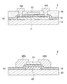
- FIG. 2 is a schematic sectional view of a thin film transistor having an Al alloy film according to the embodiment.
- FIG. 9 is a conceptual diagram illustrating observation points of composition analysis of an Al alloy ingot illustrated in Table 4.
- 6 is an optical microscope image of the aluminum alloy ingot shown in Table 5. It is an electron microscope image of the aluminum alloy ingot concerning this embodiment.
- FIGS. 1A and 1B are schematic cross-sectional views of a thin film transistor having an Al alloy film according to the present embodiment.
- the thin film transistor 1 shown in FIG. 1A is a top gate type thin film transistor.
- an active layer (semiconductor layer) 11, a gate insulating film 12, a gate electrode 13, and a protective layer 15 are stacked on a glass substrate 10.
- the active layer 11 is composed of, for example, LTPS (low temperature poly-silicon).
- the active layer 11 is electrically connected to the source electrode 16S and the drain electrode 16D.
- the thin film transistor 2 shown in FIG. 1B is a bottom gate type thin film transistor.
- a gate electrode 23, a gate insulating film 22, an active layer 21, a source electrode 26S, and a source electrode 26D are stacked on a glass substrate 20.
- the active layer 21 is made of, for example, an IGZO (In-Ga-Zn-O) -based oxide semiconductor material.
- the active layer 21 is electrically connected to the source electrode 26S and the drain electrode 26D.
- the thickness of the gate electrodes 13 and 23 is not particularly limited, and is, for example, 100 nm or more and 600 nm or less, preferably 200 nm or more and 400 nm or less. If the thickness is less than 100 nm, it is difficult to reduce the resistance of the gate electrodes 13 and 23. If the thickness exceeds 600 nm, the bending resistance of the thin film transistor 2 tends to decrease.
- the gate electrodes 13 and 23 are made of the Al alloy film according to the present embodiment.
- the specific resistance of the gate electrodes 13 and 23 (Al alloy film) is set to, for example, 15 ⁇ ⁇ cm or less, preferably 10 ⁇ ⁇ cm or less.
- the gate electrodes 13 and 23 are formed by forming a solid Al alloy film by a sputtering method and then patterning it into a predetermined shape.
- a sputtering method for example, a DC sputtering method, a pulse DC sputtering method, an RF sputtering method, or the like is applied. Either wet etching or dry etching is applied for patterning the solid Al alloy film.
- the film formation and patterning of the gate electrodes 13 and 23 are generally performed during the manufacturing process of the thin film transistors 1 and 2.
- a heat treatment (annealing) is performed as necessary.
- a heat treatment at 550 ° C. or more and 650 ° C. or less for 30 seconds or more and 30 minutes or less may be performed for activation of the active layer 11.
- the gate insulating film 22 may be subjected to heat treatment at 350 ° C. to 450 ° C. for 30 minutes to 180 minutes in order to repair the insulating property.
- a material for the gate electrodes 13 and 23 there is a method of selecting a high melting point metal (for example, Mo) that can endure such a thermal history.
- a high melting point metal for example, Mo
- a gate electrode made of a refractory metal (for example, Mo) as a base material is applied to the curved surface of such a display device, the refractory metal does not have sufficient bending resistance, and thus the refractory metal does not have sufficient bending resistance. Some of the cracks may cause the electrode to break.
- a gate electrode is applied to a curved surface portion of a display device because the gate electrode has a role of forming a channel in an opposing semiconductor layer instead of a wiring for simply passing an electric current, the gate electrode may be cracked or broken. And it is desirable to have excellent bending resistance.
- the gate electrode may have a high resistance or the gate electrode may be disconnected. Further, when another film is formed on the hillock, the film may have a high resistance or be disconnected due to the shape of the underlying hillock.
- the electrode materials constituting the gate electrodes 13 and 23 must have a bending resistance that can withstand a bending radius of 1 mm. It is required to have excellent heat resistance, in which hillocks are hardly generated, and to be able to perform etching without residue.
- an Al alloy film described below is applied as a material for the gate electrodes 13 and 23 in order to address the above problem.
- the Al alloy film according to the present embodiment uses an Al pure metal as a base material, and the Al pure metal includes at least one first additive element selected from the group consisting of Zr, Sc, Mo, Y, Nb, and Ti. It is contained.
- the content of the first additive element is adjusted to, for example, 0.01 atomic% or more and 1.0 atomic% or less, and preferably, 0.1 atomic% or more and 0.5 atomic% or less. Has been adjusted.
- Such an Al alloy film has excellent bending resistance and exhibits the effect of the addition of the first additive element.
- the Orowan stress due to the intermetallic compound acts as a barrier to dislocation line movement in the Al alloy, and even if the Al alloy film is subjected to heat treatment, plastic deformation of the Al alloy film is suppressed. As a result, hillocks hardly occur in the Al alloy film, and an Al alloy film having high heat resistance is formed.
- the gate electrodes 13 and 23 and other wiring films may have electrical defects.
- the above Al alloy film is applied to the gate electrodes 13 and 23, and a highly reliable display device can be provided.
- the content of the first additive element when the content of the first additive element is less than 0.01 atomic%, when the heat treatment is performed on the Al alloy film, the concentration of the intermetallic compound in the Al alloy film is low, and the hillock is contained in the Al alloy film. Is more likely to occur. That is, the heat resistance of the Al alloy film decreases, which is not preferable.
- the content of the first additive element when the content of the first additive element is more than 1.0 atomic%, the heat resistance is maintained, but the bending resistance of the Al alloy film is deteriorated and the specific resistance of the Al alloy film is increased. Absent.
- both wet etching and dry etching can be performed.
- Al pure metal contains at least one kind of second additive element selected from the group of Mn, Si, Cu, Ge, Mg, Ag and Ni. May be done.
- the content of the second additive element in the Al alloy film is adjusted to, for example, 0.2 to 3.0 atomic%, preferably 0.5 to 1.5 atomic%. Has been adjusted.
- the effect of the addition of the second additive element is that even if a heat treatment is performed on the Al alloy film, the second additive element is favorably dissolved in Al and the plastic deformation of the Al alloy film is suppressed.
- Al and the second additive element form an intermetallic compound in the Al alloy film. As a result, hillocks hardly occur in the Al alloy film, and an Al alloy film having high heat resistance is formed.
- the content of the second additive element is less than 0.2 atomic%, when the heat treatment is performed on the Al alloy film, the concentration of the second additive element (solid solution strengthening element) in the Al alloy film And hillocks are easily generated in the Al alloy film. That is, the heat resistance of the Al alloy film decreases, which is not preferable.
- the content of the second additive element is larger than 3.0 atomic%, the heat resistance is maintained, but the bending resistance of the Al alloy film is deteriorated and the specific resistance of the Al alloy film is increased. Absent.
- both wet etching and dry etching can be performed.
- the first and second additive elements may be added to the Al pure metal.
- the Al alloy film contains at least one first additive element selected from the group consisting of Zr, Sc, Mo, Y, Nb, and Ti in Al pure metal, and further contains Mn, Si, Cu,
- a film containing at least one second additive element selected from the group consisting of Ge, Mg, Ag and Ni may be used.
- the content of the first additive element in the Al alloy film is adjusted to, for example, 0.01 to 1.0 atomic%, preferably 0.1 to 0.5 atomic%.
- the content of the second additive element is adjusted to, for example, 0.2 atomic% or more and 3.0 atomic% or less, and preferably adjusted to 0.5 atomic% or more and 1.5 atomic% or less. I have.
- the intermetallic compound may not be sufficiently dispersed and formed. Even in such a case, since the Al alloy film already contains the second additive element (solid solution strengthening element), the Al alloy film is already in a state where hillocks are not easily formed.
- the Al alloy film is subjected to heat treatment and once the intermetallic compound is dispersed and formed in the Al alloy film, it is assumed that stress is generated in the Al alloy film due to agglomerates of Al and the second additive element. Also, the movement of dislocation lines is suppressed by the intermetallic compound of Al and the first additive element. For this reason, a hillock is not easily formed in the Al alloy.
- the Al alloy film contains at least one first additive element selected from the group consisting of Zr, Sc, Mo, Y, Nb, and Ti in an Al pure metal, and further includes Ce, Nd, La, And a film containing at least one third additive element selected from the group of Gd.
- the content of the first additive element in the Al alloy film is adjusted to, for example, 0.01 to 1.0 atomic%, preferably 0.1 to 0.5 atomic%.
- the content of the third additive element is adjusted to, for example, 0.1 atomic% or more and 1.0 atomic% or less, and preferably adjusted to 0.2 atomic% or more and 0.7 atomic% or less. I have.
- the function of the first additional element is further promoted by adding the third additional element to the Al alloy containing the first additional element.
- the third additive element is added to the Al alloy, the intermetallic compound of Al and the first additive element is more uniformly dispersed in the Al alloy.
- the third additive element has a property of precipitating toward grain boundaries when subjected to heat treatment.
- the phenomenon that the grain boundaries serve as barriers and adjacent microcrystals are connected and the crystals are coarsened is suppressed.
- stress is hardly generated in the Al alloy film, and the heat resistance of the Al alloy film is further improved.
- the content of the third additive element is less than 0.1 atomic%, the heat resistance of the Al alloy film decreases, which is not preferable.
- the content of the third additive element is larger than 1.0 atomic%, residues are easily generated when wet etching or dry etching is performed on the Al alloy film, which is not preferable.
- the Al alloy film contains at least one second additive element selected from the group consisting of Mn, Si, Cu, Ge, Mg, Ag, and Ni in Al pure metal, and further includes Ce, Nd, and La. And a film containing at least one third additive element selected from the group of Gd.
- the content of the second additive element in the Al alloy film is adjusted to, for example, 0.2 to 3.0 atomic%, preferably 0.5 to 1.5 atomic%.
- the content of the third additive element is adjusted to, for example, 0.1 atomic% or more and 1.0 atomic% or less, and preferably adjusted to 0.2 atomic% or more and 0.7 atomic% or less. I have.
- the function of the second additive element is further promoted.
- the third additive element is added to the Al alloy, the second additive element is more uniformly dispersed in the Al alloy.
- the third additive element is directed to the grain boundary by the heat treatment, in the Al alloy film, the phenomenon that adjacent fine particles are connected and the fine particles are coarsened is suppressed. As a result, stress is hardly generated in the Al alloy film, and the heat resistance of the Al alloy film is further improved.
- the Al alloy film contains at least one first additive element selected from the group consisting of Zr, Sc, Mo, Y, Nb, and Ti in Al pure metal, and further contains Mn, Si, Cu, At least one second additive element selected from the group consisting of Ge, Mg, Ag and Ni is contained, and at least one third additive element selected from the group consisting of Ce, Nd, La, and Gd is contained.
- a contained film may be used.
- the content of the first additive element in the Al alloy film is adjusted to, for example, 0.01 to 1.0 atomic%, preferably 0.1 to 0.5 atomic%.
- the content of the second additive element is adjusted to, for example, 0.2 atomic% or more and 3.0 atomic% or less, and preferably adjusted to 0.5 atomic% or more and 1.5 atomic% or less
- the content of the third additional element is adjusted to, for example, 0.1 atomic% or more and 1.0 atomic% or less, and preferably adjusted to 0.2 atomic% or more and 0.7 atomic% or less.
- Such an Al alloy film has excellent bending resistance, and the effect of the addition of the first addition element, the effect of the addition of the second addition element, and the effect of the addition of the third addition element are synergistic. It is exhibited in.
- the gate electrodes 13 and 23 made of the Al alloy film are formed, for example, by sputtering in a vacuum chamber.
- a sputtering target used for sputtering film formation an aluminum alloy target (Al alloy target) for forming the gate electrodes 13 and 23 of the thin film transistors 1 and 2 is used.
- a target having the same composition as the Al alloy film is prepared.
- a pure metal piece having a purity of 5N (99.999%) or more is formed by adding a metal piece, a metal powder, or the like of at least one of the first, second, and third additional elements. After being mixed, these mixed materials are easily prepared in a crucible by a melting method such as induction heating.
- the temperature difference between the solidus line and the liquidus line in the phase diagram of the metal compound is obtained by setting the addition amount of at least one of the first additional element, the second additional element, and the third additional element in the above range.
- an Al alloy ingot in which primary crystals of intermetallic compounds or the like are unlikely to settle in the crucible is formed. That is, in the Al alloy ingot, at least one of the first, second, and third additional elements is uniformly dispersed.
- the Al alloy ingot is subjected to plastic processing such as forging, rolling, and pressing, and the Al alloy ingot is processed into a plate shape or a disk shape, thereby producing an Al alloy target.
- the Al alloy target uses an Al pure metal as a base material, and the Al pure metal contains at least one first additive element selected from the group consisting of Zr, Sc, Mo, Y, Nb, and Ti. ing.
- the content of the first additional element is adjusted to, for example, 0.01 to 1.0 atomic%, preferably 0.1 to 0.5 atomic%. Has been adjusted.
- the Al alloy target contains, in place of the first additional element, at least one type of second additional element selected from the group consisting of Mn, Si, Cu, Ge, Mg, Ag, and Ni in Al pure metal. May be done.
- the content of the second additional element is adjusted to, for example, 0.2 to 3.0 atomic%, preferably 0.5 to 1.5 atomic%. Has been adjusted.
- the first additive element and the second additive element may be added to the Al alloy metal in the Al alloy target.
- the Al alloy target contains at least one first additive element selected from the group consisting of Zr, Sc, Mo, Y, Nb, and Ti in Al pure metal, and further contains Mn, Si, Cu, At least one second additive element selected from the group consisting of Ge, Mg, Ag and Ni may be contained.
- the content of the first additive element is adjusted to, for example, 0.01 atomic% or more and 1.0 atomic% or less, preferably, 0.1 atomic% or more and 0.5 atomic% or less.
- the content of the second additive element is adjusted to, for example, 0.2 atomic% or more and 3.0 atomic% or less, and preferably adjusted to 0.5 atomic% or more and 1.5 atomic% or less. I have.
- the Al alloy target contains at least one first additive element selected from the group consisting of Zr, Sc, Mo, Y, Nb, and Ti in pure Al metal, and further includes Ce, Nd, and La. , And at least one third additive element selected from the group of Gd.
- the content of the first additive element is adjusted to, for example, 0.01 atomic% or more and 1.0 atomic% or less, preferably, 0.1 atomic% or more and 0.5 atomic% or less.
- the content of the third additive element is adjusted to, for example, 0.1 atomic% or more and 1.0 atomic% or less, and preferably adjusted to 0.2 atomic% or more and 0.7 atomic% or less. I have.
- the Al alloy target contains at least one second additive element selected from the group consisting of Mn, Si, Cu, Ge, Mg, Ag and Ni in Al pure metal, and further contains Ce, Nd, At least one third additive element selected from the group consisting of La and Gd may be contained.
- the content of the second additional element is adjusted to, for example, 0.2 to 3.0 atomic%, preferably 0.5 to 1.5 atomic%.
- the content of the third additive element is adjusted to, for example, 0.1 atomic% or more and 1.0 atomic% or less, and preferably adjusted to 0.2 atomic% or more and 0.7 atomic% or less. I have.
- the Al alloy target contains at least one first additive element selected from the group consisting of Zr, Sc, Mo, Y, Nb, and Ti in Al pure metal, and further includes Mn, Si, and Cu. , Ge, Mg, Ag, and Ni, and at least one third additive element selected from the group consisting of Ce, Nd, La, and Gd. May be contained.
- the content of the first additive element is adjusted to, for example, 0.01 atomic% or more and 1.0 atomic% or less, preferably, 0.1 atomic% or more and 0.5 atomic% or less.
- the content of the second additive element is adjusted to, for example, 0.2 atomic% or more and 3.0 atomic% or less, and preferably adjusted to 0.5 atomic% or more and 1.5 atomic% or less
- the content of the third additional element is adjusted to, for example, 0.1 atomic% or more and 1.0 atomic% or less, and preferably adjusted to 0.2 atomic% or more and 0.7 atomic% or less.
- Al alloy film formed by sputtering using such an Al alloy target exhibits the above-described excellent effects.
- the Al ingot receives heat during plastic working such as forging, rolling, and pressing, and Al crystal grains may grow in the Al ingot.
- Al crystal grains also exist in the Al target manufactured from such an Al ingot, and during the film formation, the Al crystal grains receive heat from the plasma to form protrusions on the surface of the Al target. These projections may cause abnormal discharge, or the projections may jump out of the Al target during film formation.
- the Al alloy target of the present embodiment at least one of the first, second, and third additional elements is added to the Al pure metal in the above-described amount.
- the content of at least one of Ce, Mn, and Si in the grain boundary between the particles is increased. Is higher than at least one of Ce, Mn, and Si.
- the average particle size of the particles is adjusted to 10 ⁇ m or more and 100 ⁇ m or less. The average particle size is determined by a laser diffraction method, image analysis using an electron microscope image, or the like.
- the grain boundary serves as a barrier, and the phenomenon that the adjacent fine particles are connected and the fine particles are coarsened is suppressed.
- the heat resistance of the Al alloy target is further improved.
- the sputtering conditions for the Al alloy film are as follows. Discharge method: DC discharge Film formation temperature: room temperature (25 ° C) Film forming pressure: 0.3 Pa Film thickness: 200 nm
- the heat treatment of the Al alloy film is performed in a nitrogen atmosphere at 400 ° C. for 1 hour and further at 600 ° C. for 2 minutes.
- Table 1 shows an example of the bending characteristics of the Mo film, the Al film, and the Al alloy film.
- the unit of the concentration is atomic% (at%).
- a two-layered SiN film (200 nm) / polyimide layer (25 ⁇ m) substrate was used.
- each of the Mo film, the Al film, and the Al alloy film is formed by sputtering on the SiN film.
- the bending radius in the bending test is 1 mm.
- the test speed is 30 rpm.
- the bending was performed in the order of once, 1,000 times, 10,000 times, and 100,000 times. The presence or absence of cracks was visually determined from the image of the optical microscope.
- Table 2 shows an example of the specific resistance ( ⁇ ⁇ cm) and the surface roughness (nm) of the Al film and the Al alloy film.
- the specific resistance of the Al alloy film becomes 10 ⁇ ⁇ cm or less. It turns out that it becomes. It is also found that the specific resistance of the Al alloy film becomes 10 ⁇ ⁇ cm or less even when the second pure element of Mn and Si is contained in the Al pure metal at 0.2 at% or more and 3.0 at% or less. .
- the surface roughness is measured by AFM (Atomic Force Microscopy). The surface roughness was observed immediately after film formation (As @ Depo.), After one hour at 400 ° C., and after two minutes at 600 ° C. The measurement range is 5 ⁇ m square.
- the upper row of each column shows the Rq value (nm), and the lower row shows the PV value (nm).
- the Rq value is the root mean square height
- the PV value is the difference between the maximum height (peak) and the minimum height (valley).
- the PV value tends to increase.
- the PV value of the wiring film is preferably smaller, and more preferably, 50 nm or less. In particular, by applying an Al alloy film having a PV value of 50 nm or less to the bent portion of the display panel, even if the Al alloy film is bent, the adhesion with the upper layer of the Al alloy film is improved.
- the Al film and the Al alloy film both have a surface roughness of 50 nm or less.
- the PV value of the Al film exceeds 300 nm.
- the PV value of the Al alloy film is smaller than that of the Al film. That is, it can be determined that hillocks are less likely to grow in the Al alloy film than in the Al film even after the heat treatment.
- Table 3 shows an example of the presence or absence of a residue after the etching of the Al film and the Al alloy film.
- an etching gas is a mixed gas of Cl 2 (50 sccm) / Ar (20 sccm).
- the etching pressure is 1.0 Pa.
- the discharge power is 400 W when the substrate bias power is 200 W.
- a mixed solution of phosphoric acid / nitric acid / acetic acid / water (commonly referred to as PAN) is used.
- the liquid temperature is 40 ° C.
- an Al alloy film containing 0.5 at% of Ce as the third additive element (Al-0.5 at% Ce, Al-0.3 at% Sc-0.2 at% Zr-0. 5at% Ce, Al-0.3at% Sc-0.2at% Zr-0.5at% Ce-1.0at% Mn-0.5at% Si) enables dry etching and wet etching without any residue Has become.
- concentration of Ce increased, and in the Al alloy film with 2.0 at% Ce (Al-2.0 at% Ce), residues were generated by dry etching.
- metal materials of Al, Sc, Zr, Mn, Si, and Ce are placed in a crucible.
- each metal is set so that the component ratio of the additive element of the Al alloy target is 0.2 at% Sc, 0.1 at% Zr, 1.0 at% Mn, 0.5 at% Si, and 0.5 at% Ce.
- Materials are placed in the crucible.
- each metal material is heated to a melting temperature (for example, 1050 ° C.) higher than the melting point of the Al alloy (for example, 640 ° C.) by 400 ° C., and each metal material is melted in the crucible. You. Next, from this melting temperature, the molten metal is cooled to room temperature to form an aluminum alloy ingot. Thereafter, the aluminum alloy ingot is forged as necessary, and the aluminum alloy ingot is cut into a plate shape or a disk shape. Thereby, an Al alloy target is formed.
- a melting temperature for example, 1050 ° C.
- the melting point of the Al alloy for example, 640 ° C.
- a metal material is melted at a melting temperature slightly higher than the melting point of the metal material, and the metal material is cooled from the slightly higher melting temperature to form an alloy ingot.
- the melting temperature is set to a temperature slightly higher than the melting point, the metal material may not be sufficiently mixed.
- the metal materials are heated and melted at a melting temperature higher than the melting point of the Al alloy by 400 ° C. or more, the respective metal materials are sufficiently mixed.
- the higher the melting temperature the longer the cooling time from the melting temperature to room temperature, and the more easily the intermetallic compound is precipitated.
- the intermetallic compound is hardly precipitated in the Al alloy ingot. The element concentration has been adjusted.
- FIG. 2 is a conceptual diagram illustrating observation points in the composition analysis of the Al alloy ingot exemplified in Table 4.
- Table 4 shows an example of the concentration distribution of each element contained in the Al alloy ingot.
- FIG. 2 illustrates, for example, a semi-cylindrical Al alloy ingot 5 obtained by dividing a cylindrical Al alloy ingot (100 mm diameter ⁇ 50 mmt) into two.
- Table 4 shows the average concentration (at%) measured from the nine observation points of each element at the top position and the average value measured from the nine observation points of each element at the middle position. The concentration (at%) and the average concentration (at%) measured from nine observation points of each element at the bottom position are shown. Table 4 also shows the deviation of the average value of the concentration ⁇ 3 ⁇ .
- the composition ratio of the additive elements of the Al alloy ingot was such that Sc was 0.2 at%, Zr was 0.1 at%, and Mn was 1.0 at% at any position of top, middle, and bottom.
- Si is about 0.5 at% and Ce is about 0.5 at%, and it can be seen that in the Al alloy ingot, the respective metal materials are uniformly dispersed in the longitudinal direction and the lateral direction of the Al alloy ingot.
- Table 5 shows the Zr concentration distribution of the aluminum alloy ingot when Sc was added at 0.2 at% and Zr was added at 3.5 at%.
- the manufacturing method is the same as the aluminum alloy ingot shown in Table 4.
- Table 5 when the Zr concentration was increased to 3.5 at%, it was found that the Zr concentration increased from the top to the bottom of the aluminum alloy ingot. An optical microscope image in this case is shown in FIG.
- FIG. 3 is an optical microscope image of the aluminum alloy ingot shown in Table 5.
- FIGS. 4A and 4B are electron microscope images of the aluminum alloy ingot according to the present embodiment.
- FIG. 4A shows a surface electron microscope image of the aluminum alloy ingot shown in Table 4.
- FIG. 4B shows a surface electron microscope image of the aluminum alloy ingot shown in Table 4 after heat treatment at 600 ° C. for 2 hours.
- the right images in FIGS. 4A and 4B are images obtained by enlarging the scale of the left image.
- the aluminum alloy ingot was composed of a group of particles A having an average particle diameter of about 10 ⁇ m.
- Ce, Mn, and Si were observed at a high concentration at the grain boundary B. That is, it is found that the content of at least one of Ce, Mn, and Si in the grain boundary between the particles A is higher than the content of at least one of Ce, Mn, and Si in the particle A.
- FIG. 4 (b) shows an image obtained by performing a heat treatment at 600 ° C. for 2 hours from the state shown in FIG. 4 (a).
- the particle size is limited to about 10 ⁇ m, and the particles A do not combine with each other to grow into a giant particle, and no new particles (for example, an intermetallic compound) are precipitated in the particle A. .
- the Al alloy film is applied to the gate electrodes 13 and 23 has been described, but the Al alloy film is applied to the source / drain electrodes, other electrodes other than the source / drain electrodes, or the wiring. It is also possible.
Landscapes
- Chemical & Material Sciences (AREA)
- Engineering & Computer Science (AREA)
- Materials Engineering (AREA)
- Mechanical Engineering (AREA)
- Metallurgy (AREA)
- Organic Chemistry (AREA)
- Chemical Kinetics & Catalysis (AREA)
- Physical Vapour Deposition (AREA)
- Electrodes Of Semiconductors (AREA)
Abstract
Description
このようなアルミニウム合金ターゲットを用いて形成されたアルミニウム合金膜であれば、アルミニウム合金膜が優れた屈曲耐性を有し、優れた耐熱性を有する。また、アルミニウム合金膜は、エッチングも可能になる。
このようなアルミニウム合金ターゲットを用いて形成されたアルミニウム合金膜であれば、アルミニウム合金膜が優れた屈曲耐性を有し、さらに、優れた耐熱性を有する。また、アルミニウム合金膜は、エッチングも可能になる。
上記第2添加元素の含有量は、0.2原子%以上3.0原子%以下である。
このようなアルミニウム合金ターゲットを用いて形成されたアルミニウム合金膜であれば、アルミニウム合金膜が優れた屈曲耐性を有し、優れた耐熱性を有する。また、アルミニウム合金膜は、エッチングも可能になる。
このようなアルミニウム合金ターゲットを用いて形成されたアルミニウム合金膜であれば、アルミニウム合金膜が優れた屈曲耐性を有し、粒界に第3添加元素が析出することで優れた耐熱性を有する。また、また、アルミニウム合金膜は、エッチングも可能になる。
放電方式:DC放電
成膜温度:室温(25℃)
成膜圧力:0.3Pa
膜厚:200nm
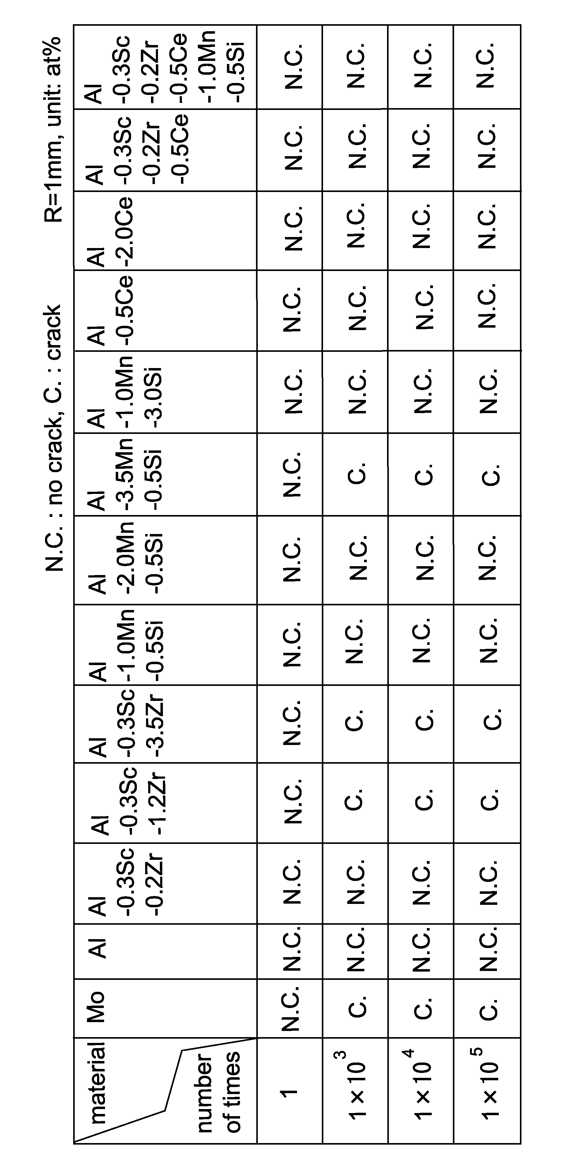

表2に示すように、Al純金属に、Sc、Zrの第1添加元素が0.01at%以上1.0at%以下含有されているときに、Al合金膜の比抵抗が10μΩ・cm以下になることが分かる。また、Al純金属に、Mn、Siの第2添加元素が0.2at%以上3.0at%以下含有されているときにも、Al合金膜の比抵抗が10μΩ・cm以下になることが分かる。
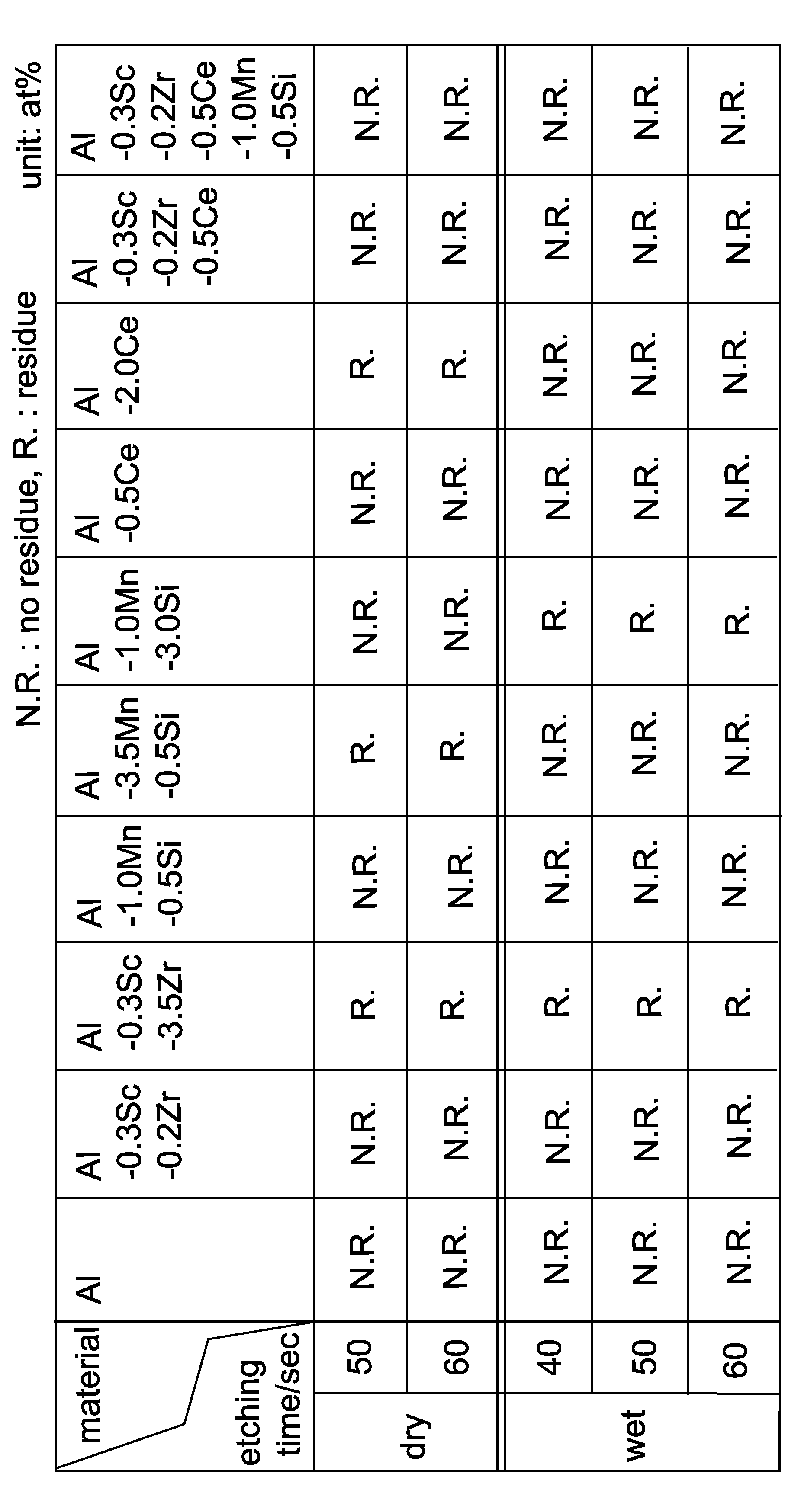
表4は、Al合金インゴットに含まれる各元素の濃度分布の一例が示されている。


10、20…ガラス基板
11、21…活性層
12、22…ゲート絶縁膜
13、23…ゲート電極
15…保護層
16D、26D…ドレイン電極
16S、26S…ソース電極
Claims (8)
- Al純金属に、Zr、Sc、Mo、Y、Nb、及びTiの群から選択される少なくとも1種の第1添加元素が含有され、
前記第1添加元素の含有量が0.01原子%以上1.0原子%以下である
アルミニウム合金ターゲット。 - 請求項1に記載されたアルミニウム合金ターゲットであって、さらに、Mn、Si、Cu、Ge、Mg、Ag及びNiの群から選択される少なくとも1種の第2添加元素が含有され、
前記第2添加元素の含有量が0.2原子%以上3.0原子%以下である
アルミニウム合金ターゲット。 - Al純金属に、Mn、Si、Cu、Ge、Mg、Ag及びNiの群から選択される少なくとも1種の第2添加元素が含有され、
前記第2添加元素の含有量が0.2原子%以上3.0原子%以下である
アルミニウム合金ターゲット。 - 請求項1~3のいずれか1つに記載されたアルミニウム合金ターゲットであって、さらに、
Ce、Nd、La、及びGdの群から選択される少なくとも1種の第3添加元素が含有され、
前記第3添加元素の含有量が0.1原子%以上1.0原子%以下である
アルミニウム合金ターゲット。 - 請求項1~4のいずれか1つに記載されたアルミニウム合金ターゲットであって、
粒子の平均粒径が10μm以上100μm以下である
アルミニウム合金ターゲット。 - 請求項5に記載されたアルミニウム合金ターゲットであって、
前記粒子間の粒界におけるCe、Mn、及びSiの少なくともいずれかの含有量が前記粒子内におけるCe、Mn、及びSiの少なくともいずれかの含有量よりも高い
アルミニウム合金ターゲット。 - Al純金属に、Zr、Sc、Mo、Y、Nb、及びTiの群から選択される少なくとも1種の第1添加元素を含有させ、塑性加工した後、切り出しを行い、前記第1添加元素の含有量が0.01原子%以上1.0原子%以下であるアルミニウム合金ターゲットを製造する製造方法。
- Al純金属に、Mn、Si、Cu、Ge、Mg、Ag及びNiの群から選択される少なくとも1種の第2添加元素が含有させ、塑性加工した後、切り出しを行い、前記第2添加元素の含有量が0.2原子%以上3.0原子%以下であるアルミニウム合金ターゲットを製造する製造方法。
Priority Applications (4)
| Application Number | Priority Date | Filing Date | Title |
|---|---|---|---|
| CN201980036620.1A CN112204165B (zh) | 2018-06-28 | 2019-03-28 | 铝合金靶材及其制造方法 |
| KR1020207037291A KR102571458B1 (ko) | 2018-06-28 | 2019-03-28 | 알루미늄 합금 타깃 및 그 제조방법 |
| US17/052,056 US20210140032A1 (en) | 2018-06-28 | 2019-03-28 | Aluminum alloy target and method of producing the same |
| JP2019547326A JP6735930B2 (ja) | 2018-06-28 | 2019-03-28 | アルミニウム合金ターゲット及びその製造方法 |
Applications Claiming Priority (2)
| Application Number | Priority Date | Filing Date | Title |
|---|---|---|---|
| JP2018123158 | 2018-06-28 | ||
| JP2018-123158 | 2018-06-28 |
Publications (1)
| Publication Number | Publication Date |
|---|---|
| WO2020003666A1 true WO2020003666A1 (ja) | 2020-01-02 |
Family
ID=68986978
Family Applications (1)
| Application Number | Title | Priority Date | Filing Date |
|---|---|---|---|
| PCT/JP2019/013503 Ceased WO2020003666A1 (ja) | 2018-06-28 | 2019-03-28 | アルミニウム合金ターゲット及びその製造方法 |
Country Status (6)
| Country | Link |
|---|---|
| US (1) | US20210140032A1 (ja) |
| JP (1) | JP6735930B2 (ja) |
| KR (1) | KR102571458B1 (ja) |
| CN (1) | CN112204165B (ja) |
| TW (1) | TWI766163B (ja) |
| WO (1) | WO2020003666A1 (ja) |
Cited By (1)
| Publication number | Priority date | Publication date | Assignee | Title |
|---|---|---|---|---|
| JP2021169662A (ja) * | 2020-04-16 | 2021-10-28 | 株式会社神戸製鋼所 | Al合金蒸着膜、ディスプレイ用配線膜、ディスプレイ装置及びスパッタリングターゲット |
Families Citing this family (2)
| Publication number | Priority date | Publication date | Assignee | Title |
|---|---|---|---|---|
| WO2024167046A1 (ko) * | 2023-02-10 | 2024-08-15 | 주식회사 큐프럼 머티리얼즈 | 박막 트랜지스터 전극 및 반사 전극용 알루미늄, 망간, 티타늄 및 실리콘을 포함하는 합금 조성물 |
| CN119640070B (zh) * | 2024-12-13 | 2025-11-28 | 先导薄膜材料(广东)有限公司 | 一种铝钪合金靶材及其制备方法 |
Citations (5)
| Publication number | Priority date | Publication date | Assignee | Title |
|---|---|---|---|---|
| JPH09228035A (ja) * | 1996-02-19 | 1997-09-02 | Hitachi Metals Ltd | 薄膜配線用Al合金膜およびAl合金スパッタリングターゲット材 |
| JPH11293454A (ja) * | 1998-04-14 | 1999-10-26 | Hitachi Metals Ltd | Al系スパッタリング用ターゲット材及びその製造方法 |
| JP2003073810A (ja) * | 2001-08-31 | 2003-03-12 | Vacuum Metallurgical Co Ltd | 薄膜アルミニウム合金及び薄膜アルミニウム合金形成用スパッタリングターゲット |
| JP2005171378A (ja) * | 2003-11-20 | 2005-06-30 | Hitachi Metals Ltd | 配線膜用Al合金膜および配線膜形成用スパッタリングターゲット材 |
| JP2012180540A (ja) * | 2011-02-28 | 2012-09-20 | Kobe Steel Ltd | 表示装置および半導体装置用Al合金膜 |
Family Cites Families (13)
| Publication number | Priority date | Publication date | Assignee | Title |
|---|---|---|---|---|
| WO1997013885A1 (fr) * | 1995-10-12 | 1997-04-17 | Kabushiki Kaisha Toshiba | Film de cablage, cible de pulverisation par bombardement ionique destinee a la formation de ce film et composant electronique comportant ce film |
| US20020014406A1 (en) * | 1998-05-21 | 2002-02-07 | Hiroshi Takashima | Aluminum target material for sputtering and method for producing same |
| US20010047838A1 (en) * | 2000-03-28 | 2001-12-06 | Segal Vladimir M. | Methods of forming aluminum-comprising physical vapor deposition targets; sputtered films; and target constructions |
| JP4237479B2 (ja) * | 2002-12-25 | 2009-03-11 | 株式会社東芝 | スパッタリングターゲット、Al合金膜および電子部品 |
| KR101124831B1 (ko) * | 2008-03-31 | 2012-03-26 | 가부시키가이샤 고베 세이코쇼 | 표시 장치, 그 제조 방법 및 스퍼터링 타깃 |
| JP5179604B2 (ja) * | 2010-02-16 | 2013-04-10 | 株式会社神戸製鋼所 | 表示装置用Al合金膜 |
| JP5524905B2 (ja) * | 2011-05-17 | 2014-06-18 | 株式会社神戸製鋼所 | パワー半導体素子用Al合金膜 |
| US9803283B1 (en) * | 2013-10-18 | 2017-10-31 | Hrl Laboratories, Llc | Method of electroless deposition of aluminum or aluminum alloy, an electroless plating composition, and an article including the same |
| WO2015108110A1 (ja) | 2014-01-15 | 2015-07-23 | 株式会社神戸製鋼所 | 薄膜トランジスタ |
| JP6377021B2 (ja) * | 2015-06-05 | 2018-08-22 | 株式会社コベルコ科研 | Al合金スパッタリングターゲット |
| US10900102B2 (en) * | 2016-09-30 | 2021-01-26 | Honeywell International Inc. | High strength aluminum alloy backing plate and methods of making |
| KR102541307B1 (ko) * | 2017-06-21 | 2023-06-13 | 오브쉬체스트보 에스 오그라니첸노이 오트벳스트베노스트유 “오베디넨나야 꼼파니야 루살 인제네르노-테크놀로지체스키 첸트르” | 알루미늄 합금 |
| KR102549527B1 (ko) * | 2018-06-28 | 2023-06-28 | 가부시키가이샤 아루박 | 알루미늄 합금 막, 그 제조방법, 및 박막 트랜지스터 |
-
2019
- 2019-03-28 WO PCT/JP2019/013503 patent/WO2020003666A1/ja not_active Ceased
- 2019-03-28 JP JP2019547326A patent/JP6735930B2/ja active Active
- 2019-03-28 US US17/052,056 patent/US20210140032A1/en not_active Abandoned
- 2019-03-28 KR KR1020207037291A patent/KR102571458B1/ko active Active
- 2019-03-28 CN CN201980036620.1A patent/CN112204165B/zh active Active
- 2019-05-28 TW TW108118305A patent/TWI766163B/zh active
Patent Citations (5)
| Publication number | Priority date | Publication date | Assignee | Title |
|---|---|---|---|---|
| JPH09228035A (ja) * | 1996-02-19 | 1997-09-02 | Hitachi Metals Ltd | 薄膜配線用Al合金膜およびAl合金スパッタリングターゲット材 |
| JPH11293454A (ja) * | 1998-04-14 | 1999-10-26 | Hitachi Metals Ltd | Al系スパッタリング用ターゲット材及びその製造方法 |
| JP2003073810A (ja) * | 2001-08-31 | 2003-03-12 | Vacuum Metallurgical Co Ltd | 薄膜アルミニウム合金及び薄膜アルミニウム合金形成用スパッタリングターゲット |
| JP2005171378A (ja) * | 2003-11-20 | 2005-06-30 | Hitachi Metals Ltd | 配線膜用Al合金膜および配線膜形成用スパッタリングターゲット材 |
| JP2012180540A (ja) * | 2011-02-28 | 2012-09-20 | Kobe Steel Ltd | 表示装置および半導体装置用Al合金膜 |
Cited By (2)
| Publication number | Priority date | Publication date | Assignee | Title |
|---|---|---|---|---|
| JP2021169662A (ja) * | 2020-04-16 | 2021-10-28 | 株式会社神戸製鋼所 | Al合金蒸着膜、ディスプレイ用配線膜、ディスプレイ装置及びスパッタリングターゲット |
| JP7427576B2 (ja) | 2020-04-16 | 2024-02-05 | 株式会社神戸製鋼所 | Al合金蒸着膜、ディスプレイ用配線膜、ディスプレイ装置及びスパッタリングターゲット |
Also Published As
| Publication number | Publication date |
|---|---|
| US20210140032A1 (en) | 2021-05-13 |
| TW202002306A (zh) | 2020-01-01 |
| TWI766163B (zh) | 2022-06-01 |
| JP6735930B2 (ja) | 2020-08-05 |
| CN112204165B (zh) | 2023-09-01 |
| CN112204165A (zh) | 2021-01-08 |
| KR102571458B1 (ko) | 2023-08-25 |
| KR20210011455A (ko) | 2021-02-01 |
| JPWO2020003666A1 (ja) | 2020-07-09 |
Similar Documents
| Publication | Publication Date | Title |
|---|---|---|
| JP6842562B2 (ja) | アルミニウム合金膜、その製造方法、及び薄膜トランジスタ | |
| CN100392505C (zh) | 铜合金薄膜、铜合金溅射靶和平板显示器 | |
| CN1479802A (zh) | 铝合金薄膜和具有该薄膜的配线电路以及形成此薄膜的靶材 | |
| TWI523087B (zh) | Al alloy film for semiconductor devices | |
| JP6735930B2 (ja) | アルミニウム合金ターゲット及びその製造方法 | |
| JP2015165563A (ja) | フラットパネルディスプレイ用配線膜、およびAl合金スパッタリングターゲット | |
| JP7133727B2 (ja) | 金属配線構造体及び金属配線構造体の製造方法 | |
| KR102677079B1 (ko) | 알루미늄 합금 타겟, 알루미늄 합금 배선막, 및 알루미늄 합금 배선막의 제조 방법 | |
| JP6947604B2 (ja) | Al合金導電膜、薄膜トランジスタ及びAl合金導電膜の製造方法 | |
| JP2007226058A (ja) | 液晶ディスプレイパネル及びその製造方法並びにCu合金スパッタリングターゲット | |
| JP2012243878A (ja) | 半導体電極構造 | |
| JP2007224397A (ja) | 平面表示パネル及びCuスパッタリングターゲット | |
| JP5510812B2 (ja) | 配線膜用Cu合金膜および配線膜形成用スパッタリングターゲット材 | |
| JP2012243877A (ja) | 半導体電極構造 |
Legal Events
| Date | Code | Title | Description |
|---|---|---|---|
| ENP | Entry into the national phase |
Ref document number: 2019547326 Country of ref document: JP Kind code of ref document: A |
|
| 121 | Ep: the epo has been informed by wipo that ep was designated in this application |
Ref document number: 19826797 Country of ref document: EP Kind code of ref document: A1 |
|
| ENP | Entry into the national phase |
Ref document number: 20207037291 Country of ref document: KR Kind code of ref document: A |
|
| NENP | Non-entry into the national phase |
Ref country code: DE |
|
| 122 | Ep: pct application non-entry in european phase |
Ref document number: 19826797 Country of ref document: EP Kind code of ref document: A1 |