WO2019244271A1 - 周波数変換器 - Google Patents
周波数変換器 Download PDFInfo
- Publication number
- WO2019244271A1 WO2019244271A1 PCT/JP2018/023444 JP2018023444W WO2019244271A1 WO 2019244271 A1 WO2019244271 A1 WO 2019244271A1 JP 2018023444 W JP2018023444 W JP 2018023444W WO 2019244271 A1 WO2019244271 A1 WO 2019244271A1
- Authority
- WO
- WIPO (PCT)
- Prior art keywords
- current
- transistor
- frequency conversion
- signal
- frequency converter
- Prior art date
- Legal status (The legal status is an assumption and is not a legal conclusion. Google has not performed a legal analysis and makes no representation as to the accuracy of the status listed.)
- Ceased
Links
Images
Classifications
-
- H—ELECTRICITY
- H03—ELECTRONIC CIRCUITRY
- H03D—DEMODULATION OR TRANSFERENCE OF MODULATION FROM ONE CARRIER TO ANOTHER
- H03D7/00—Transference of modulation from one carrier to another, e.g. frequency-changing
- H03D7/14—Balanced arrangements
-
- H—ELECTRICITY
- H04—ELECTRIC COMMUNICATION TECHNIQUE
- H04B—TRANSMISSION
- H04B1/00—Details of transmission systems, not covered by a single one of groups H04B3/00 - H04B13/00; Details of transmission systems not characterised by the medium used for transmission
- H04B1/06—Receivers
- H04B1/16—Circuits
- H04B1/26—Circuits for superheterodyne receivers
Definitions
- the present invention relates to a frequency converter, and more particularly to a frequency converter used in satellite communication, terrestrial microwave communication, mobile communication, and the like.
- Patent Document 1 discloses a Gilbert cell type conventional frequency converter.
- the Gilbert cell type frequency converter includes an input-stage transistor (hereinafter referred to as a Gm-stage transistor) that performs voltage-current conversion on an input RF (Radio-Frequency) signal, and a local oscillator (LO (Local Oscillator)).
- a switch stage transistor for performing a frequency conversion using the LO signal from the converter to convert an RF signal into an IF (Intermediate Frequency) signal, and an output stage transistor having a load impedance element for performing current-voltage conversion on the IF signal. are stacked vertically.
- the voltage of circuits has been reduced.
- the voltage headroom of the transistors becomes insufficient and the output signal is distorted.
- the voltage headroom indicates a margin of a voltage amplitude at which a signal can be extracted from an output terminal without distortion.
- Patent Document 2 discloses a frequency converter configured to directly input an RF signal to a source terminal of a switch transistor.
- the frequency converter described in Patent Literature 2 since no Gm stage transistor is provided, the number of vertically stacked transistors is smaller than that of a Gilbert cell type frequency converter. Thereby, the voltage headroom of the transistor is secured, and high linearity of the output signal can be obtained. Further, in the frequency converter disclosed in Patent Document 2, by setting the gate bias voltage of the switch-stage transistor to be high, an overdrive voltage is secured, and deterioration of linearity due to a distortion component of the transistor is suppressed.
- the Gilbert cell-type frequency converter described in Patent Document 1 has a plurality of transistors stacked vertically. Therefore, when the voltage is reduced, the voltage headroom of the transistors becomes insufficient, and the output signal becomes low. However, there was a problem that it was distorted.
- the frequency converter described in Patent Literature 2 suppresses distortion of the output signal by reducing the number of stages of vertically stacked transistors. Further, by setting the gate bias voltage of the switch-stage transistor high, high linearity of the output signal can be obtained even at a low power supply voltage. However, there is a problem that setting the gate bias voltage high increases idle current.
- the present invention has been made to solve such a problem, and an object of the present invention is to provide a frequency converter that can realize high linearity of an output signal while suppressing an idle current.
- a frequency conversion element that receives an RF signal and an LO signal, performs voltage-current conversion on the RF signal, performs frequency conversion using the LO signal, and outputs an IF signal.
- a DC potential detection circuit that detects a DC potential of the frequency conversion element that changes according to the input power of the RF signal, and applies the DC potential to the frequency conversion element based on the DC potential detected by the DC potential detection circuit.
- a bias generation circuit that generates a bias voltage to be applied to the power supply.
- the bias generation circuit is a frequency converter that increases the bias voltage in accordance with an increase in the DC potential detected by the DC potential detection circuit.
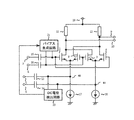
- FIG. 1 is a configuration diagram showing a configuration of a frequency converter according to Embodiment 1 of the present invention.
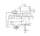
- FIG. 3 is a configuration diagram showing another configuration example of the frequency converter according to Embodiment 1 of the present invention.
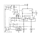
- FIG. 7 is a configuration diagram showing a configuration of a frequency converter according to Embodiment 2 of the present invention.
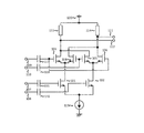
- FIG. 2 is a configuration diagram showing a configuration of a comparative example with respect to the frequency converter according to Embodiment 1 of the present invention.
- FIG. FIG. 1 is a diagram showing a configuration of the frequency converter according to Embodiment 1 of the present invention. Before describing the first embodiment, the configuration of a comparative example will be described with reference to FIG. 4 so that the features of the first embodiment can be more easily understood.
- FIG. 4 is a diagram showing a comparative example for comparison with the first embodiment.
- FIG. 4 shows a configuration of a general Gilbert cell type frequency converter as a comparative example.
- the frequency converter includes Gm-stage transistors 101 and 102, switch-stage transistors 103 to 106, RF differential signal input terminals 107 and 108, and LO differential signal input terminals 109 and 110. , IF differential signal output terminals 111 and 112, load impedance elements 113 and 114, DC cut capacitors 115 to 118, a current source 119, and a power supply terminal 120.
- the RF signals input from the RF differential signal input terminals 107 and 108 are subjected to voltage-current conversion by the Gm stage transistors 101 and 102.
- the RF signal is frequency-converted by the switch transistors 103 to 106 that perform a switching operation based on the LO signal, and becomes an IF signal.
- the IF signal is subjected to current-voltage conversion by the load impedance elements 113 and 114 and output from the IF differential signal output terminals 111 and 112.
- the Gm-stage transistor, the switch-stage transistor, and the load impedance element are vertically stacked. Therefore, as described above, when the voltage is reduced due to the miniaturization of the semiconductor process, the voltage headroom of the vertically stacked transistors becomes insufficient, and the output signal is distorted.
- the frequency converter according to the first embodiment has a configuration for solving the above-described problem.
- the frequency converter according to the first embodiment will be described.
- the frequency converter includes frequency conversion elements 1 to 4, RF differential signal input terminals 5 and 6, LO differential signal input terminals 7 and 8, an IF Differential signal output terminals 9 and 10, load impedance elements 11 and 12, DC cut capacitors 13 to 16, current sources 17 and 18, power supply terminal 19, DC potential detection circuit 20, bias generation circuit 21 It is configured with.
- LO LO signals are input to the LO differential signal input terminals 7 and 8 from an external device such as a local oscillator.
- IF differential signal output terminals 9 and 10 output IF signals to the outside.
- Each of the frequency conversion elements 1 to 4 includes, for example, an NMOS (n-Channel Metal-Oxide Semiconductor) transistor.
- NMOS n-Channel Metal-Oxide Semiconductor
- Each of the frequency conversion elements 1 to 4 has a source terminal, a gate terminal, and a drain terminal.
- the DC cut capacitor 13 is connected between the RF differential signal input terminal 5 and the source terminals of the frequency conversion elements 1 and 2.
- the DC cut capacitor 14 is connected between the RF differential signal input terminal 6 and the source terminals of the frequency conversion elements 3 and 4.
- the DC cut capacitor 15 is connected between the LO differential signal input terminal 7 and the gate terminals of the frequency conversion elements 1 and 4.
- the DC cut capacitor 16 is connected between the LO differential signal input terminal 8 and the gate terminals of the frequency conversion elements 2 and 3.
- RF An RF signal is input to the source terminal of the frequency conversion element 1 from the RF differential signal input terminal 5 via the DC cut capacitor 13. Further, a LO signal is input to the gate terminal of the frequency conversion element 1 from the LO differential signal input terminal 7 via the DC cut capacitor 15. Further, the frequency conversion element 1 outputs an IF signal from the drain terminal to the IF differential signal output terminal 10.
- An RF signal is input to the source terminal of the frequency conversion element 2 from the RF differential signal input terminal 5 via the DC cut capacitor 13. Further, an LO signal is input to the gate terminal of the frequency conversion element 2 from the LO differential signal input terminal 8 via the DC cut capacitor 16. Further, the frequency conversion element 2 outputs an IF signal from the drain terminal to the IF differential signal output terminal 9.
- An RF signal is input to the source terminal of the frequency conversion element 3 from the RF differential signal input terminal 6 via the DC cut capacitor 14. Further, the LO signal is input to the gate terminal of the frequency conversion element 3 from the LO differential signal input terminal 8 via the DC cut capacitor 16. Further, the frequency conversion element 3 outputs an IF signal from the drain terminal to the IF differential signal output terminal 10.
- An RF signal is input to the source terminal of the frequency conversion element 4 from the RF differential signal input terminal 6 via the DC cut capacitor 14. Further, a LO signal is input to the gate terminal of the frequency conversion element 4 from the LO differential signal input terminal 7 via the DC cut capacitor 15. Further, the frequency conversion element 4 outputs an IF signal from the drain terminal to the IF differential signal output terminal 9.
- the load impedance element 11 is connected between the power supply terminal 19 and the IF differential signal output terminal 10, and performs current-voltage conversion on the IF signals output from the drain terminals of the frequency conversion elements 1 and 3.
- the load impedance element 12 is connected between the power supply terminal 19 and the IF differential signal output terminal 9 and performs current-voltage conversion on the IF signals output from the drain terminals of the frequency conversion elements 2 and 4.
- connection point 40 a connection point between the current source 17 and the source terminals of the frequency conversion elements 1 and 2 is referred to as a connection point 40.
- connection point 41 a connection point between the current source 18 and the source terminals of the frequency conversion elements 3 and 4.
- the DC potential detection circuit 20 is connected between the DC cut capacitor 13 and the connection point 40, and is connected between the DC cut capacitor 14 and the connection point 41.
- the DC potential detection circuit 20 detects the DC potential at the source terminals of the frequency conversion elements 1 to 4 and outputs a signal corresponding to the detected DC potential to the bias generation circuit 21.
- the bias generation circuit 21 is connected between the DC cut capacitor 15 and the gate terminals of the frequency conversion elements 1 and 4, and is connected between the DC cut capacitor 16 and the gate terminals of the frequency conversion elements 2 and 3. I have.
- the bias generation circuit 21 controls the gate bias voltages of the frequency conversion elements 1 to 4 based on the value of the DC potential detected by the DC potential detection circuit 20. Specifically, the bias generation circuit 21 increases the gate bias voltage according to the increase in the DC potential detected by the DC potential detection circuit 20, and responds to the decrease in the DC potential detected by the DC potential detection circuit 20. To reduce the gate bias voltage.
- the relationship between the DC potential and the gate bias voltage may be represented by a linear function such as a proportional relationship, or may be represented by a non-linear function.
- the frequency converter according to the first embodiment does not include the Gm-stage transistors 101 and 102 in FIG. Therefore, in FIG. 1, since the number of vertically stacked transistors is small, the voltage headroom can be ensured and the occurrence of distortion of the IF signal can be suppressed.
- the RF signal is input from RF differential signal input terminals 5 and 6.
- the RF signal is applied to the source terminals of the frequency conversion elements 1 to 4.
- the LO signal is input from the LO differential signal input terminals 7 and 8.
- the LO signal is applied to the gate terminals of the frequency conversion elements 1 to 4.
- the frequency conversion elements 1 to 4 perform voltage-current conversion on the RF signal and perform switching operation using the LO signal to convert the frequency to an IF signal.
- the IF signal is subjected to current-voltage conversion by the load impedance elements 11 and 12 and output from IF differential signal output terminals 9 and 10.
- the DC potential detection circuit 20 detects the DC potential at the source terminals of the frequency conversion elements 1 to 4, and outputs a voltage corresponding to the detected DC potential. Further, the bias generation circuit 21 generates a gate bias voltage to be applied to the frequency conversion elements 1 to 4 according to the output voltage of the DC potential detection circuit 20.
- the currents from the current sources 17 and 18 are kept at a constant value. Therefore, when the input power input to the RF differential signal input terminals 5 and 6 (hereinafter, referred to as RF input power) increases, the DC potential at the source terminals of the frequency conversion elements 1 to 4 increases. Therefore, the gate-source voltages of the frequency conversion elements 1 to 4 decrease, and the overdrive voltage becomes insufficient. As a result, the distortion components of the signals output from the frequency conversion elements 1 to 4 increase. In order to prevent this, the distortion component of the IF signal can be suppressed by setting the gate bias voltages of the frequency conversion elements 1 to 4 high. However, the idle current increases as the gate bias voltage increases. This problem occurs in the comparative example shown in FIG.
- the following method operates so that the gate-source voltages of the frequency conversion elements 1 to 4 do not decrease even when the RF input power increases.
- the DC potential detection circuit 20 detects an increase in DC potential at the source terminals of the frequency conversion elements 1 to 4 due to an increase in RF input power.
- the DC potential detection circuit 20 outputs a voltage corresponding to the detected DC potential to the bias generation circuit 21.
- the bias generation circuit 21 increases the gate bias voltages of the frequency conversion elements 1 to 4 according to the output voltage from the DC potential detection circuit 20.
- the gate-source voltages of the frequency conversion elements 1 to 4 can be increased accordingly.
- an overdrive voltage is secured, and distortion components of the IF signal can be suppressed.
- high linearity of the IF signal can be obtained.
- the gate bias voltage during the idle operation can be set low.
- good linearity can be obtained by setting the overdrive voltage of the frequency conversion elements 1 to 4 to 0.2 V to 0.3 V.
- the gate bias voltage is reduced so as to be 2 V or less. Therefore, the frequency converter can be operated with a low idle current, so that an increase in power consumption can be suppressed.
- the gate bias voltage is increased by the amount corresponding to the increase in the RF input power, so that the power consumption during the idle operation, which occupies most of the operation period, can be suppressed.
- the frequency converter according to the first embodiment includes the DC potential detection circuit 20 that detects a change in the DC potential at the source terminals of the frequency conversion elements 1 to 4 that input the RF signal, A bias generation circuit 21 for generating a gate bias voltage.
- the gate bias voltage can be increased when the RF input power is increased. High linearity can be realized.
- the frequency conversion elements 1 to 4 include an NMOS transistor.
- the present invention is not limited to such an example, and the frequency conversion elements 1 to 4 may be, for example, bipolar transistors. (BJT: Bipolar Junction Transistor). Even in that case, the same effect can be obtained. In that case, the gate, drain and source of the NMOS transistor are replaced with the base, collector and emitter of the BJT.
- BJT Bipolar Junction Transistor
- the DC potential detection circuit 20 may be configured to output a DC voltage from a middle point of a resistor connected between the differentials. In this case, by setting the resistance value sufficiently higher than the RF input impedance, the DC potential can be detected without affecting the RF input matching.
- FIG. 2 is a circuit diagram showing a modification of the frequency converter according to the first embodiment of the present invention.
- the difference between FIG. 1 and FIG. 2 is that, in FIG. 2, the impedance elements 31 and 32 are added, and the current source 18 in FIG. 1 is not provided.
- the impedance elements 31 and 32 are connected in series.
- the connection point of the impedance elements 31 and 32 will be referred to as a connection point 42.
- the DC potential detection circuit 20 is connected between the connection point 42 and the current source 17.
- the impedance element 31 is connected to the source terminals of the frequency conversion elements 1 and 2.
- the impedance element 32 is connected to the source terminals of the frequency conversion elements 3 and 4.
- the impedance elements 31 and 32 perform RF input matching on RF signals input to the RF differential signal input terminals 5 and 6.
- the DC potential detection circuit 20 is connected to a connection point 42 between the impedance elements 31 and 32 that is a virtual ground point for the RF signal. Therefore, the DC potential detection circuit 20 can detect the DC potential fluctuation of the source terminals of the frequency conversion elements 1 to 4 without affecting the differential type RF signal.
- any of the configurations shown in FIGS. 1 and 2 may be employed. In either configuration, the same operation is performed, and the same effect is obtained.
- FIG. FIG. 3 is a diagram showing a configuration of the frequency converter according to Embodiment 2 of the present invention.
- the bias generation circuit 21 according to the first embodiment includes a temperature-proportional current source 22, a first transistor 23, The third transistor 24, 25, the fourth transistor 26, and the bias resistors 27, 28 are provided.
- the temperature-proportional current source 22 is provided in the frequency converter, and outputs a current proportional to the device temperature of the frequency converter using power from an external power supply supplied to the power supply terminal 19.
- the device temperature of the frequency converter is a junction temperature of a transistor included in the frequency converter.
- the first transistor 23 includes, for example, an NMOS transistor.
- the output voltage from the DC potential detection circuit 20 is input to the gate terminal of the first transistor 23.
- the source terminal of the first transistor 23 is grounded, and the drain terminal is connected to the second transistor 24 and the third transistor 25.
- the first transistor 23 changes the drain current output from the drain terminal according to the output voltage output from the DC potential detection circuit 20. Specifically, in the first transistor 23, when the output voltage output from the DC potential detection circuit 20 increases, the drain current output from the drain terminal increases accordingly.
- the drain current is referred to as a first current.
- the DC potential detection circuit 20 outputs a voltage according to the DC potential. Therefore, when the RF input power increases, the first current output from the first transistor 23 increases.
- the second transistor 24 and the third transistor 25 include, for example, a PMOS transistor (p-channel metal-oxide semiconductor).
- the second transistor 24 and the third transistor 25 form a current mirror circuit using the first current from the first transistor 23 as a reference current.
- the current mirror circuit is hereinafter referred to as a first current mirror circuit.
- the second transistor 24 and the third transistor 25 output the first current from the first transistor 23 at a preset current mirror ratio, and add the first current to the output current output from the temperature proportional current source 22. Let it.
- the current after the addition is referred to as a second current.
- the transistor size ratio of the second and third transistors 24 and 25 may be 1: 1 and the current mirror ratio may be 1.
- the transistor size ratio of the second and third transistors 24 and 25 is 1: M, where M is an arbitrary natural number of 2 or more.
- the current mirror ratio M may be set to 2 or more by setting the transistor size ratio to 1: M. In this case, the amount of increase in the gate bias voltage with respect to the amount of increase in the DC potential detected by the DC potential detection circuit 20 can be increased, so that higher linearity can be obtained.
- the bias resistor 27 is connected between the fourth transistor 26 and the gate terminals of the frequency conversion elements 2 and 3.
- the bias resistor 28 is connected between the fourth transistor 26 and the gate terminals of the frequency conversion elements 1 and 4.
- the fourth transistor 26 includes, for example, an NMOS transistor.
- the fourth transistor 26 and the frequency conversion elements 1 to 4 form a current mirror circuit using the second current as a reference current.
- the current mirror circuit is referred to as a second current mirror circuit.
- the second current is supplied to the fourth transistor 26.
- the fourth transistor 26 outputs a second current at a preset current mirror ratio via bias resistors 27 and 28, and applies a bias voltage to the gate terminals of the frequency conversion elements 1 to 4.
- the transistor size ratio between the fourth transistor 26 and the frequency conversion elements 1 to 4 may be 1: 1 and the current mirror ratio may be 1.
- the transistor size ratio between the fourth transistor 26 and the frequency conversion elements 1 to 4 may be 1: M.
- the first transistor 23 outputs a first current corresponding to the output voltage output from the DC potential detection circuit 20.
- the second transistor 24 and the third transistor 25 output the first current from the first transistor 23 at a preset current mirror ratio to output current output from the temperature proportional current source 22.
- the second current is output by the addition.
- the temperature proportional current source 22 outputs a current proportional to the device temperature of the frequency converter.
- the fourth transistor 26 generates a bias voltage using the second current, and applies the bias voltage to the gate terminals of the frequency conversion elements 1 to 4.
- the bias voltage is controlled according to the output voltage output from the DC potential detection circuit 20.
- the bias voltage during the idle operation can be set low. Further, even when the frequency converter operates at a low idle current, the gate bias voltage can be increased when the RF input power is increased, so that high linearity of the IF signal can be realized.
- the temperature proportional current source 22 is used.
- the gate bias voltage applied to the frequency conversion elements 1 to 4 can be made proportional to the device temperature. Thereby, even when the device temperature becomes higher than the threshold value, it is possible to suppress the deterioration of the linearity.
- the current source does not necessarily have to be a temperature proportional current source.
- a constant current source that does not depend on the device temperature may be used.
- the overdrive voltage of the frequency conversion elements 1 to 4 decreases.
- the distortion component of the output signal slightly increases.
- the linearity of the output signal of the frequency converter is slightly deteriorated as compared with that at normal temperature. Therefore, it is more desirable to use a temperature proportional current source.
- the first current output from the first transistor 23 increases according to the increase in the DC potential at the source terminals of the frequency conversion elements 1 to 4.
- the first current is added to the current supplied from the temperature-proportional current source 22 via the first current mirror circuit to become a second current.
- the second current mirror circuit applies a bias voltage to the frequency conversion elements 1 to 4 using the second current.
- the gate-source voltages of the frequency conversion elements 1 to 4 increase.
- an overdrive voltage can be secured, so that a distortion component of the output signal of the frequency converter can be suppressed.
- the linearity of the frequency converter can be improved.
- the transistor size ratio of the second and third transistors 24 and 25 may be 1: M, M may be an arbitrary natural number of 2 or more, and the current mirror ratio M may be 2 or more. In that case, the amount of increase in the gate bias voltage with respect to the amount of increase in the DC potential detected by the DC potential detection circuit 20 can be increased, so that higher linearity can be obtained.
- the bias generation circuit 21 includes the temperature-proportional current source 22. Therefore, it is possible to compensate for a rise in device temperature in the gate bias voltages of the frequency conversion elements 1 to 4. As a result, in low idle current operation, there is an effect of suppressing linearity degradation both when the RF input power is increased and when the device is at a high temperature.
- the present invention can freely combine any of the embodiments, modify any of the constituent elements of each of the embodiments, or omit any of the constituent elements of each of the embodiments. is there.
Landscapes
- Engineering & Computer Science (AREA)
- Computer Networks & Wireless Communication (AREA)
- Signal Processing (AREA)
- Power Engineering (AREA)
- Amplifiers (AREA)
Abstract
周波数変換器は、RF信号に対して、電圧-電流変換を行うとともに、LO信号を用いて周波数変換を行って、IF信号を出力する周波数変換素子1~4と、周波数変換素子1~4のDC電位を検出するDC電位検出回路20と、DC電位検出回路20により検出されたDC電位に基づいて、周波数変換素子1~4に印加するバイアス電圧を生成するバイアス生成回路21とを備え、バイアス生成回路21は、DC電位検出回路20により検出されるDC電位の増加に応じて、バイアス電圧を増加させる。
Description
この発明は周波数変換器に関し、衛星通信、地上波マイクロ波通信、移動体通信等で使用される周波数変換器に関するものである。
特許文献1には、ギルバートセル型の従来の周波数変換器が開示されている。
ギルバートセル型の周波数変換器は、入力されたRF(Radio Frequency)信号に対して電圧-電流変換を行う入力段トランジスタ(以下、Gm段トランジスタと呼ぶ)と、局部発振器(LO(Local Oscillator))からのLO信号を用いた周波数変換を行って、RF信号をIF(Intermediate Frequency)信号に変換するスイッチ段トランジスタと、IF信号に対して電流-電圧変換を行う負荷インピーダンス素子を有する出力段トランジスタとが、縦積みされて構成されている。
しかしながら、近年、半導体プロセスの微細化に伴い、回路の低電圧化が進んでいる。上述したように、ギルバートセル型の周波数変換器は、複数段のトランジスタが縦積みされているため、低電圧化が進むと、トランジスタの電圧ヘッドルームが不足し、出力信号が歪むという課題があった。なお、電圧ヘッドルームとは出力端子において歪みなく信号を取り出すことができる電圧振幅のマージンを示す。
そこで、特許文献2には、スイッチ段トランジスタのソース端子に、直接、RF信号を入力する構成の周波数変換器が開示されている。特許文献2に記載の周波数変換器では、Gm段トランジスタが設けられていないため、ギルバートセル型の周波数変換器と比較して、トランジスタの縦積みの段数が少ない。それにより、トランジスタの電圧ヘッドルームが確保され、出力信号の高い線形性を得ることができる。さらに、特許文献2の周波数変換器では、スイッチ段トランジスタのゲートバイアス電圧を高く設定することで、オーバードライブ電圧を確保し、トランジスタの歪み成分による線形性の劣化を抑制している。
上述したように、特許文献1に記載のギルバートセル型の周波数変換器は、複数段のトランジスタが縦積みされているため、低電圧化が進むと、トランジスタの電圧ヘッドルームが不足し、出力信号が歪むという課題があった。
また、特許文献2に記載の周波数変換器は、上述したように、縦積みされたトランジスタの段数を減らすことで、出力信号の歪みを抑制している。さらに、スイッチ段トランジスタのゲートバイアス電圧を高く設定することで、低電源電圧時にも、出力信号の高い線形性を得ることができる。しかしながら、ゲートバイアス電圧を高く設定することで、アイドル電流が増加してしまうという課題があった。
この発明は、かかる課題を解決するためになされたものであり、アイドル電流を抑えながら、出力信号の高い線形性を実現することが可能な、周波数変換器を提供することを目的とする。
この発明は、RF信号とLO信号とが入力され、前記RF信号に対して、電圧-電流変換を行うとともに、前記LO信号を用いて周波数変換を行って、IF信号を出力する周波数変換素子と、前記RF信号の入力電力に応じて変化する前記周波数変換素子のDC電位を検出するDC電位検出回路と、前記DC電位検出回路により検出された前記DC電位に基づいて、前記周波数変換素子に印加するバイアス電圧を生成するバイアス生成回路とを備え、前記バイアス生成回路は、前記DC電位検出回路により検出される前記DC電位の増加に応じて、前記バイアス電圧を増加させる、周波数変換器である。
この発明に係る周波数変換器によれば、アイドル電流を抑えながら、出力信号の高い線形性を実現することができる。
以下、この発明をより詳細に説明するために、この発明を実施するための実施の形態について、添付の図面にしたがって説明する。
実施の形態1.
図1は、この発明の実施の形態1に係る周波数変換器の構成を示す図である。本実施の形態1の特徴が、より分かりやすくなるように、本実施の形態1の説明を行う前に、図4を用いて、比較例の構成について説明する。
図1は、この発明の実施の形態1に係る周波数変換器の構成を示す図である。本実施の形態1の特徴が、より分かりやすくなるように、本実施の形態1の説明を行う前に、図4を用いて、比較例の構成について説明する。
図4は、本実施の形態1と比較するための比較例を示した図である。図4においては、比較例として、一般的なギルバートセル型の周波数変換器の構成を示している。図4に示すように、当該周波数変換器は、Gm段トランジスタ101,102と、スイッチ段トランジスタ103~106と、RF差動信号入力端子107,108と、LO差動信号入力端子109,110と、IF差動信号出力端子111,112と、負荷インピーダンス素子113,114と、DCカット容量115~118と、電流源119と、電源端子120とから構成されている。
次に、図4の周波数変換器の動作について説明する。RF差動信号入力端子107,108から入力されたRF信号は、Gm段トランジスタ101,102により、電圧―電流変換される。次に、当該RF信号は、LO信号に基づいてスイッチ動作を行うスイッチ段トランジスタ103~106により周波数変換されて、IF信号となる。次に、当該IF信号は、負荷インピーダンス素子113,114により、電流―電圧変換されて、IF差動信号出力端子111,112から出力される。
このように、図4に示すギルバートセル型の周波数変換器では、Gm段トランジスタ、スイッチ段トランジスタおよび負荷インピーダンス素子が縦積みされて構成されている。そのため、上述したように、半導体プロセスの微細化に伴う低電圧化が進むと、縦積みされたトランジスタの電圧ヘッドルームが不足し、出力信号が歪むという課題があった。
そのため、本実施の形態1に係る周波数変換器は、上記の課題を解決するための構成を有している。以下、本実施の形態1に係る周波数変換器について説明する。
図1に示すように、本実施の形態1に係る周波数変換器は、周波数変換素子1~4と、RF差動信号入力端子5,6と、LO差動信号入力端子7,8と、IF差動信号出力端子9,10と、負荷インピーダンス素子11,12と、DCカット容量13~16と、電流源17,18と、電源端子19と、DC電位検出回路20と、バイアス生成回路21とを備えて構成されている。
以下、図1の各構成要素について説明する。
RF差動信号入力端子5,6には、外部から、RF信号が入力される。
LO差動信号入力端子7,8には、局部発振器などの外部機器から、LO信号が入力される。
IF差動信号出力端子9,10は、外部に対して、IF信号を出力する。
周波数変換素子1~4は、それぞれ、例えばNMOS(n-Channel Metal-Oxide Semiconductor)トランジスタを備えて構成される。各周波数変換素子1~4は、ソース端子、ゲート端子、および、ドレイン端子を有している。
DCカット容量13は、RF差動信号入力端子5と周波数変換素子1,2のソース端子との間に接続されている。
DCカット容量14は、RF差動信号入力端子6と周波数変換素子3,4のソース端子との間に接続されている。
DCカット容量15は、LO差動信号入力端子7と周波数変換素子1,4のゲート端子との間に接続されている。
DCカット容量16は、LO差動信号入力端子8と周波数変換素子2,3のゲート端子との間に接続されている。
周波数変換素子1のソース端子には、RF差動信号入力端子5から、DCカット容量13を介して、RF信号が入力される。また、周波数変換素子1のゲート端子には、LO差動信号入力端子7から、DCカット容量15を介して、LO信号が入力される。また、周波数変換素子1は、ドレイン端子から、IF差動信号出力端子10に対して、IF信号を出力する。
また、周波数変換素子2のソース端子には、RF差動信号入力端子5から、DCカット容量13を介して、RF信号が入力される。また、周波数変換素子2のゲート端子には、LO差動信号入力端子8から、DCカット容量16を介して、LO信号が入力される。また、周波数変換素子2は、ドレイン端子から、IF差動信号出力端子9に対して、IF信号を出力する。
また、周波数変換素子3のソース端子には、RF差動信号入力端子6から、DCカット容量14を介して、RF信号が入力される。また、周波数変換素子3のゲート端子には、LO差動信号入力端子8から、DCカット容量16を介して、LO信号が入力される。また、周波数変換素子3は、ドレイン端子から、IF差動信号出力端子10に対して、IF信号を出力する。
また、周波数変換素子4のソース端子には、RF差動信号入力端子6から、DCカット容量14を介して、RF信号が入力される。また、周波数変換素子4のゲート端子には、LO差動信号入力端子7から、DCカット容量15を介して、LO信号が入力される。また、周波数変換素子4は、ドレイン端子から、IF差動信号出力端子9に対して、IF信号を出力する。
負荷インピーダンス素子11は、電源端子19とIF差動信号出力端子10との間に接続され、周波数変換素子1,3のドレイン端子から出力されたIF信号に対して、電流-電圧変換を行う。
負荷インピーダンス素子12は、電源端子19とIF差動信号出力端子9との間に接続され、周波数変換素子2,4のドレイン端子から出力されたIF信号に対して、電流-電圧変換を行う。
電流源17は、周波数変換素子1,2のソース端子に接続されている。以下では、電流源17と、周波数変換素子1,2のソース端子との接続点を、接続点40と呼ぶこととする。
電流源18は、周波数変換素子3,4のソース端子に接続されている。以下では、電流源18と、周波数変換素子3,4のソース端子との接続点を、接続点41と呼ぶこととする。
DC電位検出回路20は、DCカット容量13と接続点40との間に接続されているとともに、DCカット容量14と接続点41との間に接続されている。DC電位検出回路20は、周波数変換素子1~4のソース端子におけるDC電位を検出し、検出したDC電位に応じた信号を、バイアス生成回路21に対して出力する。
バイアス生成回路21は、DCカット容量15と周波数変換素子1,4のゲート端子との間に接続されるとともに、DCカット容量16と周波数変換素子2,3のゲート端子との間に接続されている。バイアス生成回路21は、DC電位検出回路20で検出されたDC電位の値に基づいて、周波数変換素子1~4のゲートバイアス電圧を制御する。具体的には、バイアス生成回路21は、DC電位検出回路20で検出されるDC電位の増加に応じて、ゲートバイアス電圧を増加させ、DC電位検出回路20で検出されるDC電位の減少に応じて、ゲートバイアス電圧を減少させる。DC電位とゲートバイアス電圧との関係は、比例関係などの線形関数で表わせてもよく、あるいは、非線形関数で表わせてもよい。
ここで、本実施の形態1に係る周波数変換器は、図1と図4とを比較すると分かるように、図1においては、図4のGm段トランジスタ101,102を備えていない。そのため、図1においては、トランジスタの縦積みの段数が少ないため、電圧ヘッドルームを確保して、IF信号の歪みの発生を抑制することができる。
次に、図1に示した本実施の形態1に係る周波数変換器の動作について説明する。RF信号は、RF差動信号入力端子5,6から入力される。当該RF信号は、周波数変換素子1~4のソース端子に印加される。また、LO信号は、LO差動信号入力端子7,8から入力される。当該LO信号は、周波数変換素子1~4のゲート端子に印加される。これにより、周波数変換素子1~4は、RF信号に対して、電圧―電流変換を行うとともに、LO信号を用いてスイッチング動作を行ってIF信号に周波数変換する。当該IF信号は、負荷インピーダンス素子11,12により、電流―電圧変換されて、IF差動信号出力端子9,10から出力される。このとき、DC電位検出回路20は、周波数変換素子1~4のソース端子におけるDC電位を検出し、検出したDC電位に応じた電圧を出力する。また、バイアス生成回路21は、DC電位検出回路20の出力電圧に応じて、周波数変換素子1~4に印加するゲートバイアス電圧を生成する。
次に、本実施の形態1に係る周波数変換器の動作原理について説明する。
電流源17,18からの電流は、一定値に保持されている。そのため、RF差動信号入力端子5,6に入力される入力電力(以下、RF入力電力と呼ぶ)が増加すると、周波数変換素子1~4のソース端子におけるDC電位が増加する。そのため、周波数変換素子1~4のゲート―ソース間電圧が低下し、オーバードライブ電圧が不足する。これにより、周波数変換素子1~4から出力される信号の歪み成分が増加する。これを防止するために、周波数変換素子1~4のゲートバイアス電圧を高く設定することで、IF信号の歪み成分を抑制することができる。しかしながら、ゲートバイアス電圧の増加に伴い、アイドル電流が増加してしまう。図4の比較例では、この問題が発生する。
そのため、本実施の形態1では、以下の方法により、RF入力電力が増加した場合においても、周波数変換素子1~4のゲート―ソース間電圧が低下しないように動作する。
実施の形態1に係る周波数変換器では、DC電位検出回路20が、RF入力電力の増加に伴う周波数変換素子1~4のソース端子におけるDC電位の増加を検出する。DC電位検出回路20は、検出したDC電位に応じた電圧を、バイアス生成回路21に出力する。バイアス生成回路21は、DC電位検出回路20からの出力電圧に応じて、周波数変換素子1~4のゲートバイアス電圧を増加させる。
このようにして、実施の形態1に係る周波数変換器では、RF入力電力の増加時に、それに応じて、周波数変換素子1~4のゲート―ソース間電圧を増加させることができる。その結果、オーバードライブ電圧が確保され、IF信号の歪み成分を抑制することができる。これにより、IF信号の高い線形性を得ることができる。
また、上述のように、バイアス生成回路21が、ゲートバイアス電圧を制御するため、アイドル動作時のゲートバイアス電圧は低く設定しておくことが可能である。例えば、RF入力電力の増加時には周波数変換素子1~4のオーバードライブ電圧を0.2V~0.3Vとすることで良好な線形性を得ることができるが、アイドル動作時にはオーバードライブ電圧が0.2V以下となるようにゲートバイアス電圧を減少させる。そのため、周波数変換器を低アイドル電流で動作させることができるので、消費電力の増加を抑制することができる。
また、RF入力電力が増加した場合には、それに応じて、ゲートバイアス電圧を増加させることで、高い線形性を得ることができる。また、RF入力電力が増加した分に合わせて、その分だけ、ゲートバイアス電圧を増加させるため、動作期間の大半を占めるアイドル動作時の消費電力を抑制することができる。
以上のように、本実施の形態1に係る周波数変換器は、RF信号を入力する周波数変換素子1~4のソース端子におけるDC電位変化を検出するDC電位検出回路20と、検出結果に応じてゲートバイアス電圧を生成するバイアス生成回路21とを備えている。これにより、アイドル動作時のバイアス電圧を低く設定して、周波数変換器を低アイドル電流動作とした場合においても、RF入力電力の増加時には、ゲートバイアス電圧を増加させることができるので、IF信号の高い線形性を実現することができる。
なお、本実施の形態1では、周波数変換素子1~4が、NMOSトランジスタを備えて構成される例を挙げて説明したが、その場合に限らず、周波数変換素子1~4は、例えばバイポーラトランジスタ(BJT:Bipolar Junction Transistor)を備えて構成されていてもよい。その場合においても、同じ効果が得られる。その場合、NMOSトランジスタにおけるゲート、ドレイン、ソースは、BJTにおけるベース、コレクタ、エミッタに置き換わる。
また、本実施の形態1におけるDC電位検出回路20は、差動間に接続した抵抗の中点からDC電圧を出力する構成としても良い。その場合、RF入力インピーダンスと比較して十分に高い抵抗値とすることで、RF入力整合に影響を与えることなくDC電位を検出することができる。
図2は、この発明の本実施の形態1に係る周波数変換器の変形例を示す回路図である。図1と図2との違いは、図2においては、インピーダンス素子31,32が追加されており、また、図1の電流源18が設置されていない。インピーダンス素子31,32は直列接続されている。以下では、インピーダンス素子31,32の接続点を、接続点42と呼ぶこととする。また、DC電位検出回路20は、接続点42と電流源17との間に接続されている。
インピーダンス素子31は、周波数変換素子1,2のソース端子に接続されている。インピーダンス素子32は、周波数変換素子3,4のソース端子に接続されている。インピーダンス素子31,32は、RF差動信号入力端子5,6に入力されるRF信号に対して、RF入力整合を行う。また、DC電位検出回路20は、RF信号に対して仮想接地点となるインピーダンス素子31,32の接続点42に接続されている。そのため、DC電位検出回路20は、差動形式のRF信号に影響を与えることなく、周波数変換素子1~4のソース端子のDC電位変動を検出することができる。
本実施の形態1においては、図1および図2のいずれの構成にしてもよい。いずれの構成においても、同様の動作を行い、同様の効果が得られる。
実施の形態2.
図3は、この発明の実施の形態2に係る周波数変換器の構成を示す図である。実施の形態2に係る周波数変換器においては、図3に示すように、上記の実施の形態1におけるバイアス生成回路21を、温度比例電流源22と、第1のトランジスタ23と、第2及び第3のトランジスタ24,25と、第4のトランジスタ26と、バイアス抵抗27,28とを備えて構成している。
図3は、この発明の実施の形態2に係る周波数変換器の構成を示す図である。実施の形態2に係る周波数変換器においては、図3に示すように、上記の実施の形態1におけるバイアス生成回路21を、温度比例電流源22と、第1のトランジスタ23と、第2及び第3のトランジスタ24,25と、第4のトランジスタ26と、バイアス抵抗27,28とを備えて構成している。
以下、バイアス生成回路21の各構成要素について説明する。
温度比例電流源22は、周波数変換器内に設けられ、電源端子19に供給される外部電源からの電力を用いて、周波数変換器のデバイス温度に比例する電流を出力する。なお、周波数変換器のデバイス温度とは、周波数変換器を構成するトランジスタの接合温度である。
第1のトランジスタ23は、例えばNMOSトランジスタを備えて構成されている。第1のトランジスタ23のゲート端子には、DC電位検出回路20からの出力電圧が入力さされる。第1のトランジスタ23のソース端子は接地され、ドレイン端子は、第2のトランジスタ24および第3のトランジスタ25に接続されている。第1のトランジスタ23は、DC電位検出回路20から出力される出力電圧に応じて、ドレイン端子から出力するドレイン電流を変化させる。具体的には、第1のトランジスタ23においては、DC電位検出回路20から出力される出力電圧が増加した場合、それに応じて、ドレイン端子から出力するドレイン電流が増加する。以下、当該ドレイン電流を、第1の電流と呼ぶこととする。
ここで、実施の形態1で説明したように、RF入力電力の増加時には、周波数変換素子1~4のソース端子におけるDC電位が増加する。DC電位検出回路20は、DC電位に応じた電圧を出力する。そのため、RF入力電力の増加時には、第1のトランジスタ23から出力される第1の電流が増加する。
また、第2のトランジスタ24と第3のトランジスタ25とは、例えばPMOSトランジスタ(p-Channel Metal-Oxide Semiconductor)を備えて構成されている。第2のトランジスタ24と第3のトランジスタ25とは、第1のトランジスタ23からの第1の電流を基準電流として、カレントミラー回路を構成している。当該カレントミラー回路を、以下では、第1のカレントミラー回路と呼ぶこととする。第2のトランジスタ24および第3のトランジスタ25は、第1のトランジスタ23からの第1の電流を予め設定されたカレントミラー比で出力して、温度比例電流源22から出力される出力電流に加算させる。以下では、この加算後の電流を、第2の電流と呼ぶこととする。
なお、第2および第3のトランジスタ24,25のトランジスタサイズ比は、1:1として、カレントミラー比を1としてもよい。あるいは、第2および第3のトランジスタ24,25のトランジスタサイズ比を1:Mとし、ここで、Mは2以上の任意の自然数とする。このように、トランジスタサイズ比を1:Mに設定することで、カレントミラー比Mを2以上としてもよい。その場合には、DC電位検出回路20によって検出されたDC電位の増加量に対するゲートバイアス電圧の増加量を大きくすることができるので、より高い線形性を得ることができる。
バイアス抵抗27は、第4のトランジスタ26と周波数変換素子2,3のゲート端子との間に接続されている。
バイアス抵抗28は、第4のトランジスタ26と周波数変換素子1,4のゲート端子との間に接続されている。
第4のトランジスタ26は、例えばNMOSトランジスタを備えて構成されている。第4のトランジスタ26と周波数変換素子1~4とは、第2の電流を基準電流として、カレントミラー回路を構成している。以下では、当該カレントミラー回路を、第2のカレントミラー回路と呼ぶこととする。第4のトランジスタ26には、第2の電流が供給される。第4のトランジスタ26は、バイアス抵抗27,28を介して、第2の電流を予め設定されたカレントミラー比で出力して、バイアス電圧を周波数変換素子1~4のゲート端子に印加する。なお、第4のトランジスタ26と周波数変換素子1~4のトランジスタサイズ比は、1:1として、カレントミラー比を1としてもよい。あるいは、第4のトランジスタ26と周波数変換素子1~4のトランジスタサイズ比を1:Mとしてもよい。
次に、本実施の形態2に係る周波数変換器の動作について説明する。
第1のトランジスタ23は、DC電位検出回路20から出力される出力電圧に応じた第1の電流を出力する。第2のトランジスタ24および第3のトランジスタ25は、第1のトランジスタ23からの第1の電流を、予め設定されたカレントミラー比で出力して、温度比例電流源22から出力される出力電流に加算させて、第2の電流を出力する。このとき、温度比例電流源22は、周波数変換器のデバイス温度に比例した電流を出力する。第4のトランジスタ26は、第2の電流を用いて、バイアス電圧を生成し、このバイアス電圧を、周波数変換素子1~4のゲート端子に印加する。
このように、本実施の形態2においても、実施の形態1と同様に、DC電位検出回路20から出力される出力電圧に応じてバイアス電圧を制御するようにしたため、実施の形態1と同様に、アイドル動作時のバイアス電圧を低く設定しておくことができる。また、周波数変換器を低アイドル電流動作とした場合においても、RF入力電力増加時には、ゲートバイアス電圧を増加させることができるので、IF信号の高い線形性を実現することができる。
さらに、本実施の形態2では、温度比例電流源22を用いている。本実施の形態2では、温度比例電流源22を設けることで、周波数変換素子1~4に与えるゲートバイアス電圧をデバイス温度に比例させることができる。これにより、デバイス温度が閾値よりも高くなった場合においても、線形性の劣化を抑制することができる。
なお、電流源は、必ずしも温度比例電流源でなくてもよい。温度比例電流源でなく、デバイス温度に依存しない定電流源を用いるようにしてもよい。しかしながら、定電流源で電流を供給する場合には、デバイス温度が予め設定された閾値以上に上昇すると、周波数変換素子1~4のオーバードライブ電圧が低下する。これにより、出力信号の歪み成分がやや増加する。このように、デバイス温度が上昇すると、常温時と比較して、周波数変換器の出力信号の線形性がやや劣化するため、温度比例電流源を用いることが、より望ましい。
以上のように、本実施の形態2においても、DC電位検出回路20とバイアス生成回路21とを備えるようにしたので、上記の実施の形態1と同様の効果を得ることができる。
本実施の形態2では、RF入力電力の増加時には、周波数変換素子1~4のソース端子におけるDC電位の増加に応じて、第1のトランジスタ23から出力される第1の電流が増加する。第1の電流は、第1のカレントミラー回路を介して、温度比例電流源22から供給される電流に加算されて、第2の電流となる。次に、第2のカレントミラー回路が、第2の電流を用いて、周波数変換素子1~4にバイアス電圧を印加する。その結果、実施の形態1と同様に、周波数変換素子1~4のゲート-ソース間電圧が増加する。これにより、オーバードライブ電圧が確保できるので、周波数変換器の出力信号の歪み成分を抑制することができる。以上により、周波数変換器の線形性を向上させることができる。
さらに、実施の形態2においては、第2および第3のトランジスタ24,25のトランジスタサイズ比を1:Mとし、Mは2以上の任意の自然数として、カレントミラー比Mを2以上としてもよい。その場合、DC電位検出回路20によって検出されたDC電位の増加量に対するゲートバイアス電圧の増加量を大きくすることができるので、より高い線形性を得ることができる。
さらに、本実施の形態2によれば、バイアス生成回路21が、温度比例電流源22を備えている。そのため、周波数変換素子1~4のゲートバイアス電圧において、デバイス温度の上昇分を補償することができる。これにより、低アイドル電流動作において、RF入力電力の増加時およびデバイス高温時の両方の場合の線形性の劣化を抑制する効果がある。
本発明は、当該発明の範囲内において、各実施の形態の自由な組み合わせ、あるいは、各実施の形態の任意の構成要素の変形、もしくは、各実施の形態において任意の構成要素の省略が可能である。
1,2,3,4 周波数変換素子、5,6 RF差動信号入力端子、7,8 LO差動信号入力端子、9,10 IF差動信号出力端子、11,12 負荷インピーダンス素子、13,14,15,16 DCカット容量、17,18 電流源、19 電源端子、20 DC電位検出回路、21 バイアス生成回路、22 温度比例電流源、23 第1のトランジスタ、24 第2のトランジスタ、25 第3のトランジスタ、26 第4のトランジスタ、27,28 バイアス抵抗、31,32 インピーダンス素子。
Claims (5)
- RF信号とLO信号とが入力され、前記RF信号に対して、電圧-電流変換を行うとともに、前記LO信号を用いて周波数変換を行って、IF信号を出力する周波数変換素子と、
前記RF信号の入力電力に応じて変化する前記周波数変換素子のDC電位を検出するDC電位検出回路と、
前記DC電位検出回路により検出された前記DC電位に基づいて、前記周波数変換素子に印加するバイアス電圧を生成するバイアス生成回路と
を備え、
前記バイアス生成回路は、前記DC電位検出回路により検出される前記DC電位の増加に応じて、前記バイアス電圧を増加させる、
周波数変換器。 - 前記バイアス生成回路は、
電流源と、
前記DC電位検出回路により検出される前記DC電位に応じた第1の電流を出力する第1のトランジスタと、
前記第1の電流を基準電流として第1のカレントミラー回路を構成して、予め設定されたカレントミラー比に基づいて、前記第1の電流を、前記電流源から供給される電流に加算することで、第2の電流を出力する第2のトランジスタおよび第3のトランジスタと、
前記第2の電流を基準電流として前記周波数変換素子と共に、第2のカレントミラー回路を構成して、前記周波数変換素子に印加する前記バイアス電圧を生成する、第4のトランジスタと
を有する、請求項1に記載の周波数変換器。 - 前記第2のトランジスタと前記第3のトランジスタとのサイズ比は1:1に設定され、前記カレントミラー比は1である、
請求項2に記載の周波数変換器。 - 前記第2のトランジスタと前記第3のトランジスタとのサイズ比は1:Mに設定され、ここで、Mは2以上の任意の自然数であり、前記カレントミラー比はMである、
請求項2記載の周波数変換器。 - 前記電流源は、前記周波数変換器の内部温度に比例する電流を出力する温度比例電流源から構成されている、
請求項2から4までのいずれか1項に記載の周波数変換器。
Priority Applications (2)
| Application Number | Priority Date | Filing Date | Title |
|---|---|---|---|
| PCT/JP2018/023444 WO2019244271A1 (ja) | 2018-06-20 | 2018-06-20 | 周波数変換器 |
| JP2020525144A JP6771852B2 (ja) | 2018-06-20 | 2018-06-20 | 周波数変換器 |
Applications Claiming Priority (1)
| Application Number | Priority Date | Filing Date | Title |
|---|---|---|---|
| PCT/JP2018/023444 WO2019244271A1 (ja) | 2018-06-20 | 2018-06-20 | 周波数変換器 |
Publications (1)
| Publication Number | Publication Date |
|---|---|
| WO2019244271A1 true WO2019244271A1 (ja) | 2019-12-26 |
Family
ID=68982779
Family Applications (1)
| Application Number | Title | Priority Date | Filing Date |
|---|---|---|---|
| PCT/JP2018/023444 Ceased WO2019244271A1 (ja) | 2018-06-20 | 2018-06-20 | 周波数変換器 |
Country Status (2)
| Country | Link |
|---|---|
| JP (1) | JP6771852B2 (ja) |
| WO (1) | WO2019244271A1 (ja) |
Citations (4)
| Publication number | Priority date | Publication date | Assignee | Title |
|---|---|---|---|---|
| JPH10242764A (ja) * | 1997-02-21 | 1998-09-11 | Toshiba Corp | ミキサー回路 |
| JP2007306208A (ja) * | 2006-05-10 | 2007-11-22 | Sony Corp | 送信装置並びに利得可変周波数変換回路 |
| JP2011507456A (ja) * | 2007-12-18 | 2011-03-03 | クゥアルコム・インコーポレイテッド | I−qミスマッチの較正及び方法 |
| JP2012090134A (ja) * | 2010-10-21 | 2012-05-10 | Renesas Electronics Corp | 高周波信号処理装置 |
-
2018
- 2018-06-20 JP JP2020525144A patent/JP6771852B2/ja active Active
- 2018-06-20 WO PCT/JP2018/023444 patent/WO2019244271A1/ja not_active Ceased
Patent Citations (4)
| Publication number | Priority date | Publication date | Assignee | Title |
|---|---|---|---|---|
| JPH10242764A (ja) * | 1997-02-21 | 1998-09-11 | Toshiba Corp | ミキサー回路 |
| JP2007306208A (ja) * | 2006-05-10 | 2007-11-22 | Sony Corp | 送信装置並びに利得可変周波数変換回路 |
| JP2011507456A (ja) * | 2007-12-18 | 2011-03-03 | クゥアルコム・インコーポレイテッド | I−qミスマッチの較正及び方法 |
| JP2012090134A (ja) * | 2010-10-21 | 2012-05-10 | Renesas Electronics Corp | 高周波信号処理装置 |
Also Published As
| Publication number | Publication date |
|---|---|
| JP6771852B2 (ja) | 2020-10-21 |
| JPWO2019244271A1 (ja) | 2020-12-17 |
Similar Documents
| Publication | Publication Date | Title |
|---|---|---|
| US20070052474A1 (en) | Amplifier and device having amplifier, and mutual conductance control method | |
| US8988154B2 (en) | Voltage-to-current converter and voltage controlled oscillator having voltage-to-current converter | |
| US8030972B2 (en) | High-speed latched comparator circuit with variable positive feedback | |
| US8791758B1 (en) | Apparatus and methods for buffer linearization | |
| US7948294B2 (en) | Mixer with high linearity | |
| US9503022B2 (en) | Balanced up-conversion mixer | |
| US20130027017A1 (en) | Voltage to current converting circuit | |
| US10574200B2 (en) | Transconductance amplifier | |
| US7295068B2 (en) | Increasing the linearity of a transconductance cell | |
| US10812059B2 (en) | Comparator | |
| US20240088847A1 (en) | Amplification circuit and communication device | |
| JP6771852B2 (ja) | 周波数変換器 | |
| US7425868B2 (en) | Apparatus and method for canceling DC output offset | |
| US20030042945A1 (en) | Frequency converter | |
| US11171612B2 (en) | Gain modulation circuit | |
| KR101764659B1 (ko) | 넓은 튜닝 범위를 갖는 고선형 전압-전류 컨버터 및 이를 이용한 전압제어발진기 | |
| US7009442B2 (en) | Linear multiplier circuit | |
| JPH1065461A (ja) | 差動増幅回路 | |
| WO2017175296A1 (ja) | 増幅器 | |
| JP2010130555A (ja) | ボルテージフォロワ回路 | |
| EP2124336B1 (en) | High-speed latched comparator circuit | |
| Sessa et al. | Robust GaN two-stage operational transconductance amplifier using dynamic voltage shifter | |
| CN113595512B (zh) | 高线性度低噪声放大器 | |
| TWI600995B (zh) | 電壓箝制電路 | |
| EP4622096A1 (en) | Passive mixer circuit |
Legal Events
| Date | Code | Title | Description |
|---|---|---|---|
| 121 | Ep: the epo has been informed by wipo that ep was designated in this application |
Ref document number: 18923349 Country of ref document: EP Kind code of ref document: A1 |
|
| ENP | Entry into the national phase |
Ref document number: 2020525144 Country of ref document: JP Kind code of ref document: A |
|
| NENP | Non-entry into the national phase |
Ref country code: DE |
|
| 122 | Ep: pct application non-entry in european phase |
Ref document number: 18923349 Country of ref document: EP Kind code of ref document: A1 |