WO2019243951A1 - 撮像装置及びその動作方法、並びに電子機器 - Google Patents
撮像装置及びその動作方法、並びに電子機器 Download PDFInfo
- Publication number
- WO2019243951A1 WO2019243951A1 PCT/IB2019/054838 IB2019054838W WO2019243951A1 WO 2019243951 A1 WO2019243951 A1 WO 2019243951A1 IB 2019054838 W IB2019054838 W IB 2019054838W WO 2019243951 A1 WO2019243951 A1 WO 2019243951A1
- Authority
- WO
- WIPO (PCT)
- Prior art keywords
- transistor
- circuit
- layer
- imaging device
- conductive layer
- Prior art date
- Legal status (The legal status is an assumption and is not a legal conclusion. Google has not performed a legal analysis and makes no representation as to the accuracy of the status listed.)
- Ceased
Links
Images








Classifications
-
- H—ELECTRICITY
- H10—SEMICONDUCTOR DEVICES; ELECTRIC SOLID-STATE DEVICES NOT OTHERWISE PROVIDED FOR
- H10F—INORGANIC SEMICONDUCTOR DEVICES SENSITIVE TO INFRARED RADIATION, LIGHT, ELECTROMAGNETIC RADIATION OF SHORTER WAVELENGTH OR CORPUSCULAR RADIATION
- H10F39/00—Integrated devices, or assemblies of multiple devices, comprising at least one element covered by group H10F30/00, e.g. radiation detectors comprising photodiode arrays
- H10F39/80—Constructional details of image sensors
- H10F39/803—Pixels having integrated switching, control, storage or amplification elements
- H10F39/8037—Pixels having integrated switching, control, storage or amplification elements the integrated elements comprising a transistor
-
- H—ELECTRICITY
- H10—SEMICONDUCTOR DEVICES; ELECTRIC SOLID-STATE DEVICES NOT OTHERWISE PROVIDED FOR
- H10F—INORGANIC SEMICONDUCTOR DEVICES SENSITIVE TO INFRARED RADIATION, LIGHT, ELECTROMAGNETIC RADIATION OF SHORTER WAVELENGTH OR CORPUSCULAR RADIATION
- H10F39/00—Integrated devices, or assemblies of multiple devices, comprising at least one element covered by group H10F30/00, e.g. radiation detectors comprising photodiode arrays
- H10F39/80—Constructional details of image sensors
- H10F39/803—Pixels having integrated switching, control, storage or amplification elements
-
- H—ELECTRICITY
- H04—ELECTRIC COMMUNICATION TECHNIQUE
- H04N—PICTORIAL COMMUNICATION, e.g. TELEVISION
- H04N25/00—Circuitry of solid-state image sensors [SSIS]; Control thereof
- H04N25/50—Control of the SSIS exposure
- H04N25/53—Control of the integration time
- H04N25/531—Control of the integration time by controlling rolling shutters in CMOS SSIS
-
- H—ELECTRICITY
- H04—ELECTRIC COMMUNICATION TECHNIQUE
- H04N—PICTORIAL COMMUNICATION, e.g. TELEVISION
- H04N25/00—Circuitry of solid-state image sensors [SSIS]; Control thereof
- H04N25/50—Control of the SSIS exposure
- H04N25/53—Control of the integration time
- H04N25/532—Control of the integration time by controlling global shutters in CMOS SSIS
-
- H—ELECTRICITY
- H04—ELECTRIC COMMUNICATION TECHNIQUE
- H04N—PICTORIAL COMMUNICATION, e.g. TELEVISION
- H04N25/00—Circuitry of solid-state image sensors [SSIS]; Control thereof
- H04N25/70—SSIS architectures; Circuits associated therewith
- H04N25/76—Addressed sensors, e.g. MOS or CMOS sensors
- H04N25/77—Pixel circuitry, e.g. memories, A/D converters, pixel amplifiers, shared circuits or shared components
- H04N25/771—Pixel circuitry, e.g. memories, A/D converters, pixel amplifiers, shared circuits or shared components comprising storage means other than floating diffusion
-
- H—ELECTRICITY
- H04—ELECTRIC COMMUNICATION TECHNIQUE
- H04N—PICTORIAL COMMUNICATION, e.g. TELEVISION
- H04N25/00—Circuitry of solid-state image sensors [SSIS]; Control thereof
- H04N25/70—SSIS architectures; Circuits associated therewith
- H04N25/76—Addressed sensors, e.g. MOS or CMOS sensors
- H04N25/78—Readout circuits for addressed sensors, e.g. output amplifiers or A/D converters
-
- H—ELECTRICITY
- H04—ELECTRIC COMMUNICATION TECHNIQUE
- H04N—PICTORIAL COMMUNICATION, e.g. TELEVISION
- H04N25/00—Circuitry of solid-state image sensors [SSIS]; Control thereof
- H04N25/70—SSIS architectures; Circuits associated therewith
- H04N25/79—Arrangements of circuitry being divided between different or multiple substrates, chips or circuit boards, e.g. stacked image sensors
-
- H—ELECTRICITY
- H10—SEMICONDUCTOR DEVICES; ELECTRIC SOLID-STATE DEVICES NOT OTHERWISE PROVIDED FOR
- H10D—INORGANIC ELECTRIC SEMICONDUCTOR DEVICES
- H10D30/00—Field-effect transistors [FET]
- H10D30/60—Insulated-gate field-effect transistors [IGFET]
- H10D30/67—Thin-film transistors [TFT]
-
- H—ELECTRICITY
- H10—SEMICONDUCTOR DEVICES; ELECTRIC SOLID-STATE DEVICES NOT OTHERWISE PROVIDED FOR
- H10D—INORGANIC ELECTRIC SEMICONDUCTOR DEVICES
- H10D30/00—Field-effect transistors [FET]
- H10D30/60—Insulated-gate field-effect transistors [IGFET]
- H10D30/67—Thin-film transistors [TFT]
- H10D30/674—Thin-film transistors [TFT] characterised by the active materials
- H10D30/6755—Oxide semiconductors, e.g. zinc oxide, copper aluminium oxide or cadmium stannate
-
- H—ELECTRICITY
- H10—SEMICONDUCTOR DEVICES; ELECTRIC SOLID-STATE DEVICES NOT OTHERWISE PROVIDED FOR
- H10D—INORGANIC ELECTRIC SEMICONDUCTOR DEVICES
- H10D84/00—Integrated devices formed in or on semiconductor substrates that comprise only semiconducting layers, e.g. on Si wafers or on GaAs-on-Si wafers
- H10D84/01—Manufacture or treatment
- H10D84/0123—Integrating together multiple components covered by H10D12/00 or H10D30/00, e.g. integrating multiple IGBTs
- H10D84/0126—Integrating together multiple components covered by H10D12/00 or H10D30/00, e.g. integrating multiple IGBTs the components including insulated gates, e.g. IGFETs
-
- H—ELECTRICITY
- H10—SEMICONDUCTOR DEVICES; ELECTRIC SOLID-STATE DEVICES NOT OTHERWISE PROVIDED FOR
- H10D—INORGANIC ELECTRIC SEMICONDUCTOR DEVICES
- H10D84/00—Integrated devices formed in or on semiconductor substrates that comprise only semiconducting layers, e.g. on Si wafers or on GaAs-on-Si wafers
- H10D84/01—Manufacture or treatment
- H10D84/02—Manufacture or treatment characterised by using material-based technologies
- H10D84/03—Manufacture or treatment characterised by using material-based technologies using Group IV technology, e.g. silicon technology or silicon-carbide [SiC] technology
- H10D84/038—Manufacture or treatment characterised by using material-based technologies using Group IV technology, e.g. silicon technology or silicon-carbide [SiC] technology using silicon technology, e.g. SiGe
-
- H—ELECTRICITY
- H10—SEMICONDUCTOR DEVICES; ELECTRIC SOLID-STATE DEVICES NOT OTHERWISE PROVIDED FOR
- H10F—INORGANIC SEMICONDUCTOR DEVICES SENSITIVE TO INFRARED RADIATION, LIGHT, ELECTROMAGNETIC RADIATION OF SHORTER WAVELENGTH OR CORPUSCULAR RADIATION
- H10F39/00—Integrated devices, or assemblies of multiple devices, comprising at least one element covered by group H10F30/00, e.g. radiation detectors comprising photodiode arrays
- H10F39/80—Constructional details of image sensors
- H10F39/802—Geometry or disposition of elements in pixels, e.g. address-lines or gate electrodes
-
- H—ELECTRICITY
- H10—SEMICONDUCTOR DEVICES; ELECTRIC SOLID-STATE DEVICES NOT OTHERWISE PROVIDED FOR
- H10F—INORGANIC SEMICONDUCTOR DEVICES SENSITIVE TO INFRARED RADIATION, LIGHT, ELECTROMAGNETIC RADIATION OF SHORTER WAVELENGTH OR CORPUSCULAR RADIATION
- H10F39/00—Integrated devices, or assemblies of multiple devices, comprising at least one element covered by group H10F30/00, e.g. radiation detectors comprising photodiode arrays
- H10F39/80—Constructional details of image sensors
- H10F39/806—Optical elements or arrangements associated with the image sensors
- H10F39/8063—Microlenses
-
- H—ELECTRICITY
- H10—SEMICONDUCTOR DEVICES; ELECTRIC SOLID-STATE DEVICES NOT OTHERWISE PROVIDED FOR
- H10F—INORGANIC SEMICONDUCTOR DEVICES SENSITIVE TO INFRARED RADIATION, LIGHT, ELECTROMAGNETIC RADIATION OF SHORTER WAVELENGTH OR CORPUSCULAR RADIATION
- H10F39/00—Integrated devices, or assemblies of multiple devices, comprising at least one element covered by group H10F30/00, e.g. radiation detectors comprising photodiode arrays
- H10F39/80—Constructional details of image sensors
- H10F39/809—Constructional details of image sensors of hybrid image sensors
-
- H—ELECTRICITY
- H10—SEMICONDUCTOR DEVICES; ELECTRIC SOLID-STATE DEVICES NOT OTHERWISE PROVIDED FOR
- H10F—INORGANIC SEMICONDUCTOR DEVICES SENSITIVE TO INFRARED RADIATION, LIGHT, ELECTROMAGNETIC RADIATION OF SHORTER WAVELENGTH OR CORPUSCULAR RADIATION
- H10F39/00—Integrated devices, or assemblies of multiple devices, comprising at least one element covered by group H10F30/00, e.g. radiation detectors comprising photodiode arrays
- H10F39/80—Constructional details of image sensors
- H10F39/811—Interconnections
Definitions
- One embodiment of the present invention relates to an imaging device, an operation method thereof, and an electronic device.
- one embodiment of the present invention is not limited to the above technical field.
- the technical field of one embodiment of the present invention disclosed in this specification and the like relates to an object, a method, or a manufacturing method.
- one embodiment of the present invention relates to a process, a machine, a manufacturer, or a composition (composition of matter). Therefore, more specifically, the technical field of one embodiment of the present invention disclosed in this specification includes a semiconductor device, a display device, a liquid crystal display device, a light-emitting device, a lighting device, a power storage device, a storage device, an imaging device, A driving method or a manufacturing method thereof can be given as an example.
- a semiconductor device in this specification and the like refers to all devices that can function by utilizing semiconductor characteristics.
- a transistor and a semiconductor circuit are one embodiment of a semiconductor device.
- the storage device, the display device, the imaging device, and the electronic device sometimes include a semiconductor device.
- Patent Document 1 discloses an imaging device in which a transistor including an oxide semiconductor and having extremely low off-state current is used for a pixel circuit.
- Patent Document 2 discloses an imaging apparatus that can be applied to a high-speed camera and can perform imaging at short time intervals.
- the held imaging data is sequentially read out, thereby realizing imaging at short time intervals. I have. Therefore, as the number of pieces of imaging data acquired at one time is larger, the number of pixels that can be used to acquire and hold one piece of imaging data decreases, and the resolution of an image corresponding to the acquired imaging data decreases.
- An object of one embodiment of the present invention is to provide an imaging device capable of acquiring a plurality of pieces of imaging data at short time intervals. Another object is to provide an imaging device which operates at high speed. Another object is to provide an imaging device capable of acquiring imaging data corresponding to a high-resolution image. Another object is to provide an imaging device capable of acquiring imaging data corresponding to a high-quality image. Another object is to provide an imaging device with a high aperture ratio. Another object is to provide a highly sensitive imaging device. Alternatively, it is an object to provide an imaging device with low power consumption. Another object is to provide a low-priced imaging device. Another object is to provide a highly reliable imaging device. Another object is to provide a novel imaging device. Another object is to provide a novel semiconductor device or the like.
- Another object is to provide an operation method of an imaging device capable of acquiring a plurality of pieces of imaging data at short time intervals. Another object is to provide an operation method of an imaging device which operates at high speed. Another object is to provide an operation method of an imaging device capable of acquiring imaging data corresponding to high-resolution imaging data. Another object is to provide an operation method of an imaging device capable of acquiring imaging data corresponding to a high-quality image. Another object is to provide an operation method of an imaging device with a high aperture ratio. Another object is to provide a highly sensitive operation method of an imaging device. Another object is to provide an operation method of an imaging device with low power consumption. Another object is to provide a low-cost operation method of an imaging device. Another object is to provide a highly reliable operation method of an imaging device. Another object is to provide a novel operation method of an imaging device. Another object is to provide a new operation method of a semiconductor device or the like.
- One embodiment of the present invention is an imaging device in which a first layer, a second layer, and a third layer are stacked, and the first layer includes a photoelectric conversion element.
- the second layer has a first circuit
- the third layer has a second circuit
- one electrode of the photoelectric conversion element is electrically connected to the first circuit
- One electrode of the photoelectric conversion element is electrically connected to a second circuit
- the first circuit holds first imaging data which is data corresponding to illuminance of light emitted to the photoelectric conversion element.
- the second circuit is an imaging device having a function of holding second imaging data, which is data corresponding to illuminance of light emitted to the photoelectric conversion element.
- the first circuit has a first transfer transistor
- the second circuit has a second transfer transistor
- one electrode of the photoelectric conversion element is a first transfer transistor.
- one electrode of the photoelectric conversion element may be electrically connected to one of the source and the drain of the second transfer transistor.
- one of the source and the drain of the first transfer transistor has a region overlapping with one of the source and the drain of the second transfer transistor, and the other of the source or the drain of the second transfer transistor is
- the transistor may have a region overlapping with the other of the source and the drain of the second transfer transistor, and the gate of the first transfer transistor may have a region overlapping with the gate of the second transfer transistor.
- the first and second transfer transistors each include a metal oxide in a channel formation region, and the metal oxide includes an element M (M is Al, Ga, Y, or Sn) and Zn. And may be provided.
- the first circuit and the second circuit may have the same configuration.
- the second layer has a first A / D converter
- the third layer has a second A / D converter
- the first A / D converter and the second A / D converter may have regions overlapping each other.
- the first layer includes a multiplexer circuit and an AD converter circuit, and a first input terminal of the multiplexer circuit is electrically connected to the first circuit, The second input terminal may be electrically connected to the second circuit, and the output terminal of the multiplexer circuit may be electrically connected to the AD conversion circuit.
- the first circuit includes a first transfer transistor, a first reset transistor, a first amplification transistor, and a first selection transistor, and includes a first transfer transistor.
- the other of the source and the drain is electrically connected to one of the source and the drain of the first reset transistor, and the one of the source and the drain of the first reset transistor is electrically connected to the gate of the first amplifying transistor.
- one of the source and the drain of the first amplification transistor may be electrically connected to one of the source and the drain of the first selection transistor.
- the first transfer transistor, the first reset transistor, the first amplification transistor, and the first selection transistor each include a metal oxide in a channel formation region; May include an element M (M is Al, Ga, Y, or Sn) and Zn.
- the second circuit includes a second transfer transistor, a second reset transistor, a second amplification transistor, and a second selection transistor, and includes a second transfer transistor.
- the other of the source and the drain is electrically connected to one of the source and the drain of the second reset transistor, and the one of the source and the drain of the second reset transistor is electrically connected to the gate of the second amplifying transistor.
- one of the source and the drain of the second amplification transistor may be electrically connected to one of the source and the drain of the second selection transistor.
- the second transfer transistor, the second reset transistor, the second amplifying transistor, and the second select transistor each include a metal oxide in a channel formation region; May include an element M (M is Al, Ga, Y, or Sn) and Zn.
- a period during which the imaging device acquires the first imaging data may be different from a period during which the imaging device acquires the second imaging data.
- an electronic device including the imaging device of one embodiment of the present invention and a display device is also one embodiment of the present invention.
- a first layer including a photoelectric conversion element, a second layer including a first circuit, and a third layer including a second circuit are stacked.
- the first imaging data which is data corresponding to the illuminance of light emitted to the photoelectric conversion element during the first period, and holds the first imaging data in the first circuit;
- second imaging data which is data corresponding to the illuminance of the light emitted to the photoelectric conversion element, is acquired and held in the second circuit
- the first circuit This is an operation method of the imaging apparatus for reading out the first imaging data held in the second circuit and the second imaging data held in the second circuit.
- an operation method of an imaging device in which a first AD conversion circuit is provided in a second layer and a second AD conversion circuit is provided in a third layer.
- the first AD conversion circuit converts the first image data as analog data into digital data
- the second AD conversion circuit converts the second image data as analog data into digital data. Good.
- one embodiment of the present invention is an operation method of an imaging device in which a photoelectric conversion element, a first circuit, and a second circuit are stacked, and the photoelectric conversion element is provided in the first period.
- First image data which is data corresponding to the illuminance of light applied to the element, is acquired and held in the first circuit, and in the second period, corresponding to the illuminance of light applied to the photoelectric conversion element.
- the second imaging data which is data to be acquired, is acquired and held in the second circuit, the first imaging data held in the first circuit is read out in the third period, and the second imaging data is read out in the fourth period.
- an operation method of the imaging device for reading the second imaging data held in the second circuit.
- the AD conversion circuit is provided in the first layer.
- the AD conversion circuit converts the first imaging data that is analog data into digital data.
- the AD conversion circuit may convert the second imaging data, which is analog data, into digital data in the fourth period.
- the first imaging data may be obtained by the global shutter method in the first period
- the second imaging data may be obtained by the global shutter method in the second period.
- an imaging device which can acquire a plurality of imaging data at short time intervals can be provided.
- an imaging device that operates at high speed can be provided.
- an imaging device capable of acquiring imaging data corresponding to a high-resolution image can be provided.
- an imaging device capable of acquiring imaging data corresponding to a high-quality image can be provided.
- an imaging device with a high aperture ratio can be provided.
- a highly sensitive imaging device can be provided.
- an imaging device with low power consumption can be provided.
- an inexpensive imaging device can be provided.
- a highly reliable imaging device can be provided.
- a novel imaging device can be provided.
- a novel semiconductor device or the like can be provided.
- an operation method of an imaging device capable of acquiring a plurality of pieces of imaging data at short time intervals.
- an operation method of an imaging device which operates at high speed can be provided.
- an operation method of an imaging device with a high aperture ratio can be provided.
- a highly sensitive operation method of an imaging device can be provided.
- an operation method of an imaging device with low power consumption can be provided.
- a low-cost operation method of an imaging device can be provided.
- a highly reliable operation method of an imaging device can be provided.
- a novel operation method of an imaging device can be provided.
- an operation method of a novel semiconductor device or the like can be provided.
- FIG. 2 is a block diagram illustrating a configuration example of an imaging device.
- FIG. 2 is a circuit diagram illustrating a configuration example of an imaging device.
- FIG. 2 is a circuit diagram illustrating a configuration example of an imaging device.
- 9 is a timing chart illustrating an example of an operation method of an imaging device.
- FIG. 2 is a block diagram illustrating a configuration example of an imaging device.
- FIGS. 4A and 4B are diagrams illustrating operations of a rolling shutter system and a global shutter system.
- FIG. 2 is a cross-sectional view illustrating a configuration example of an imaging device.
- FIGS. 3A and 3B are cross-sectional views illustrating a structure example of a transistor.
- FIG. 1A is a cross-sectional view illustrating a configuration example of an imaging device.
- FIG. 4B is a cross-sectional view illustrating a configuration example of a photoelectric conversion element.
- (A), (B), (C) Perspective view showing a configuration example of an imaging device.
- FIG. 3A is a top view illustrating a structural example of a transistor.
- FIGS. 4B and 4C are cross-sectional views illustrating a configuration example of a transistor.
- FIGS. FIG. 3A is a top view illustrating a structural example of a transistor.
- FIGS. 4B and 4C are cross-sectional views illustrating a configuration example of a transistor.
- FIGS. FIG. 1A is a cross-sectional view illustrating a configuration example of an imaging device.
- FIG. 4B is a cross-sectional view illustrating a configuration example of a photo
- FIGS. 4B and 4C are cross-sectional views illustrating a configuration example of a transistor.
- FIGS. FIG. 3A is a top view illustrating a structural example of a transistor.
- FIGS. 4B and 4C are cross-sectional views illustrating a configuration example of a transistor.
- FIGS. FIG. 3A is a top view illustrating a structural example of a transistor.
- FIGS. 4B and 4C are cross-sectional views illustrating a configuration example of a transistor.
- FIGS. (A1), (A2), (A3) A perspective view of a package containing an imaging device.
- 7A, 7B, 7C, 7D, and 7E illustrate electronic devices.
- 7A, 7B, 7C, and 7D illustrate electronic devices.
- the term “film” and the term “layer” can be interchanged with each other.
- the term “conductive layer” may be changed to the term “conductive film” in some cases.
- the term “insulating film” can be changed to the term “insulating layer”.
- a term indicating an arrangement such as “above” or “below” does not limit that the positional relationship between components is “directly above” or “directly below”.
- the expression “a gate over a gate insulating layer (a gate terminal, a gate region, or a gate electrode)” does not exclude a component including another component between the gate insulating layer and the gate.
- ordinal numbers such as “first”, “second”, and “third” are given in order to avoid confusion of components, and are not limited in number.
- the term “electrically connected” includes the case where components are connected through an "object having any electric function".
- the “something having an electrical action” includes a switching element such as a transistor, a resistor, an inductor, a capacitor, an element having various functions, and the like, in addition to an electrode and a wiring.
- a transistor is an element having at least three terminals, including a gate, a drain, and a source.
- a channel formation region is provided between the drain (drain terminal, drain region, or drain electrode) and the source (source terminal, source region, or source electrode), and the source and the drain are connected to each other through the channel formation region.
- a current can flow between them.
- a channel formation region refers to a region through which current mainly flows.
- the functions of the source and the drain may be switched when transistors with different polarities are used or when the direction of current changes in circuit operation. For this reason, in this specification and the like, the terms of source and drain can be used interchangeably.
- off-state current refers to drain current when a transistor is in an off state (also referred to as a non-conductive state or a cut-off state) unless otherwise specified.
- the off state refers to a state in which the gate voltage Vgs with respect to the source is lower than the threshold voltage Vth in the case of an n-channel transistor, and the gate voltage Vgs with respect to the source in the case of a p-channel transistor. The state is higher than the voltage Vth. That is, the off-state current of an n-channel transistor may be a drain current when the voltage Vgs of the gate with respect to the source is lower than the threshold voltage Vth.
- the drain may be read as a source. That is, the off-state current sometimes refers to a source current when the transistor is in an off state. Further, the term “leak current” may be used in the same meaning as the off current. In this specification and the like, off-state current sometimes refers to current flowing between a source and a drain when a transistor is off.
- metal oxide is a metal oxide in a broad sense.
- Metal oxides are classified into oxide insulators, oxide conductors (including transparent oxide conductors), oxide semiconductors (also referred to as oxide semiconductors), and the like.
- the metal oxide may be referred to as an oxide semiconductor in some cases. That is, when the metal oxide has at least one of an amplifying action, a rectifying action, and a switching action, the metal oxide can be referred to as a metal oxide semiconductor (metal oxide semiconductor). That is, a transistor including a metal oxide in a channel formation region can be referred to as an "oxide semiconductor transistor" or an "OS transistor.” Similarly, the above-described “transistor using an oxide semiconductor” is a transistor including a metal oxide in a channel formation region.
- a metal oxide containing nitrogen may also be referred to as a metal oxide. Further, a metal oxide containing nitrogen may be referred to as metal oxynitride. Details of the metal oxide will be described later.
- One embodiment of the present invention is an imaging device including a pixel provided with a photoelectric conversion element and n (n is an integer of 2 or more) holding circuits.
- the photoelectric conversion element and the n holding circuits are provided to be stacked on each other.
- One electrode of the photoelectric conversion element is electrically connected to the first to n-th holding circuits.
- the holding circuit has a function of holding imaging data.
- the holding circuit includes an OS transistor having an extremely low off-state current, and can hold imaging data for a long time.
- imaging data refers to data corresponding to illuminance of light emitted to a photoelectric conversion element.
- An imaging device of one embodiment of the present invention has a function of acquiring imaging data and writing the data to a holding circuit. Further, the imaging device of one embodiment of the present invention has a function of reading imaging data held in a holding circuit, performing analog-to-digital conversion (hereinafter, AD conversion), and outputting the result to the outside of the imaging device.
- AD conversion analog-to-digital conversion
- An operation method of the imaging device of one embodiment of the present invention is as follows. First, in a first period, the imaging device acquires first imaging data and writes the first imaging data into the first holding circuit. Similarly, in the second to n-th periods, the imaging device acquires the second to n-th imaging data and writes the data to the second to n-th holding circuits. After that, the first to n-th imaging data held in the first to n-th holding circuits are read. The read image data is A / D converted as described above and output to the outside of the imaging device. The above is the operation method of the imaging device of one embodiment of the present invention.
- the holding circuit included in the imaging device of one embodiment of the present invention can hold imaging data for a long time. Therefore, there is no need to read out the imaging data from the holding circuit immediately after the imaging device acquires one piece of imaging data and writes it into the holding circuit, and n pieces of imaging data (first to n-th imaging data) After these are obtained, these imaging data can be read. That is, the reading of n pieces of imaging data can be performed collectively. This makes it possible to acquire a plurality of pieces of imaging data at shorter time intervals than in the case where acquisition and reading of one piece of imaging data are performed alternately. Therefore, the imaging device of one embodiment of the present invention can be applied to, for example, a high-speed camera.
- the imaging device of one embodiment of the present invention can have low power consumption while acquiring a plurality of pieces of imaging data at short time intervals.
- the first to n-th holding circuits included in the imaging device of one embodiment of the present invention are provided to be stacked with each other. For this reason, even when n pieces of image data are read out collectively, image data corresponding to an image having the same resolution as that when reading out image data one by one can be obtained.
- the imaging device of one embodiment of the present invention can achieve both acquisition of a plurality of imaging data at short time intervals and acquisition of imaging data corresponding to a high-resolution image.
- FIG. 1 is a block diagram illustrating a configuration example of an imaging device 10 which is an imaging device of one embodiment of the present invention.
- the imaging device 10 includes a layer 20 and n layers (n is an integer of 2 or more) of layers 30 provided above the layer 20. That is, the layer 20 and the n-layers 30 are provided in a stacked manner.
- the n layers 30 are distinguished by being described as layers 30_1 to 30_n, respectively.
- the lowermost one of the n layers 30 is referred to as a layer 30_1 and is provided above the layers 30_2 to 30_n in this order.
- the uppermost layer 30 may be the layer 30_1 and may be provided below the layers 30_2 to 30_n in this order.
- “_i” is added to a code indicating a component such as a circuit provided in the layer 30 — i (i is an integer of 1 or more and n or less) to indicate the layer 30 provided with the component. I have.
- the photoelectric conversion elements 21 are arranged in a matrix in the layer 20.
- a photodiode can be used as the photoelectric conversion element 21, charges corresponding to the illuminance of the light are accumulated.
- the layer 30 includes an imaging unit 31, a gate driver circuit 33, a source driver circuit 34, and an AD conversion circuit 35.
- the holding circuits 32 are arranged in a matrix in the imaging unit 31.
- the gate driver circuit 33 and the source driver circuit 34 can have a configuration including, for example, a shift register circuit.
- the holding circuits 32 having the same number of rows and the same number of columns as the photoelectric conversion elements 21 are provided. Since the imaging device 10 has n layers 30, the imaging device 10 can be provided with n times as many holding circuits 32 as the number of the photoelectric conversion elements 21.
- the holding circuit 32 can be provided so as to have a region overlapping with the photoelectric conversion element 21.
- one gate driver circuit 33, one source driver circuit 34, and one AD conversion circuit 35 can be provided.
- the imaging device 10 is provided with n gate driver circuits 33, source driver circuits 34, and AD conversion circuits 35 each.
- One or more of the gate driver circuit 33, the source driver circuit 34, and the AD conversion circuit 35 may be provided in one layer 30.
- One electrode of the photoelectric conversion element 21 is electrically connected to the holding circuits 32_1 to 32_n.
- one electrode of the photoelectric conversion element 21 is electrically connected to the holding circuits 32_1 to 32_n having a region overlapping with the photoelectric conversion element 21.
- the gate driver circuit 33 is electrically connected to the holding circuit 32.
- the AD conversion circuit 35 is electrically connected to the holding circuit 32 via the wiring 40.
- the source driver circuit 34 is electrically connected to the AD conversion circuit 35.
- the holding circuits 32_1 to 32_n can be provided so as to have regions overlapping with each other.
- One pixel is formed by one photoelectric conversion element 21 having an overlapping region and the holding circuits 32_1 to 32_n.
- the gate driver circuits 33_1 to 33_n can be provided so as to have overlapping regions.
- the source driver circuits 34_1 to 34_n can be provided so as to have regions overlapping with each other.
- the AD conversion circuits 35_1 to 35_n can be provided so as to have mutually overlapping regions.
- the holding circuit 32 has a function of holding image data.
- the gate driver circuit 33 has a function of generating a selection signal for controlling the operation of the holding circuit 32. By supplying the selection signal to the holding circuit 32, for example, the holding circuit 32 for writing image data and the holding circuit 32 for reading the held image data can be selected.
- the gate driver circuit 33 can select the holding circuit 32 for each row.
- the source driver circuit 34 has, for example, a function of selecting the holding circuit 32 that reads out the held image data.
- the source driver circuit 34 can select the holding circuit 32 for each column. As described above, the imaging data held in the holding circuit 32 in the row selected by the gate driver circuit 33 and in the column selected by the source driver circuit 34 can be read.
- the AD conversion circuit 35 has a function of converting image data, which is analog data, read from the holding circuit 32 into digital data, and outputting the digital data as a signal OUT to the outside of the image capturing apparatus 10.
- the signal OUT can be output to, for example, a display device. Alternatively, it can be output to a storage device, a communication device, or the like.
- the imaging data read from the holding circuit 32 is supplied to the AD conversion circuit 35 via the wiring 40. That is, it can be said that the wiring 40 has a function as a data line.
- FIG. 2 is a circuit diagram illustrating a configuration example of the holding circuit 32 and a connection relationship with the photoelectric conversion element 21.
- the holding circuit 32 includes the transistor 12, the transistor 13, the transistor 14, the transistor 15, and the capacitor 16. Note that a structure without the capacitor 16 may be employed.
- One electrode of the photoelectric conversion element 21 is electrically connected to one of the source and the drain of the transistor 12.
- the other of the source and the drain of the transistor 12 is electrically connected to one of the source and the drain of the transistor 13.
- One of a source and a drain of the transistor 13 is electrically connected to a gate of the transistor 14.
- the gate of the transistor 14 is electrically connected to one electrode of the capacitor 16.
- One of a source and a drain of the transistor 14 is electrically connected to one of a source and a drain of the transistor 15.
- FIG. 2 illustrates a configuration in which the cathode of the photoelectric conversion element 21 is electrically connected to one of the source and the drain of the transistor 12 and the anode of the photoelectric conversion element 21 is electrically connected to the wiring 47.
- the anode of the photoelectric conversion element 21 may be electrically connected to one of the source and the drain of the transistor 12, and the cathode of the photoelectric conversion element 21 may be electrically connected to the wiring 47.
- a point where the other of the source or the drain of the transistor 12, the one of the source or the drain of the transistor 13, the gate of the transistor 14, and the one electrode of the capacitor 16 is electrically connected is referred to as a node FD.
- the gate of the transistor 12 is electrically connected to the wiring 41.
- the gate of the transistor 13 is electrically connected to the wiring 42.
- the gate of the transistor 15 is electrically connected to the wiring 43.
- the other of the source and the drain of the transistor 13 is electrically connected to the wiring 44.
- the other of the source and the drain of the transistor 14 is electrically connected to the wiring 40.
- the other of the source and the drain of the transistor 15 is electrically connected to the wiring 45.
- the other electrode of the capacitor 16 is electrically connected to the wiring 46.
- the other electrode of the photoelectric conversion element 21 is electrically connected to the wiring 47.
- the wiring 41, the wiring 42, and the wiring 43 each have a function as a scanning line for controlling on / off of the transistor 12, the transistor 13, and the transistor 15, and are not illustrated in FIG. Connected.
- a constant potential can be supplied to the wirings 44 to 47.
- a power supply potential can be supplied.
- the wirings 44 to 47 have a function as power supply lines.
- a high potential can be supplied to the wirings 44 and 45, and a low potential can be supplied to the wirings 46 and 47, respectively.
- the potential supplied to the wiring 44 is referred to as a potential VR. Note that when the anode of the photoelectric conversion element 21 is electrically connected to one of the source and the drain of the transistor 12 and the cathode of the photoelectric conversion element 21 is electrically connected to the wiring 47, A low potential can be supplied to the wirings 44 and 46.
- the low potential can be a ground potential or a negative potential, for example.
- the high potential can be higher than the low potential.
- the transistor 12 has a function as a transfer transistor that controls transfer of charge accumulated in the photoelectric conversion element 21 to light from the photoelectric conversion element 21 to the node FD.
- the transistor 12 When the transistor 12 is turned on, the charge stored in the photoelectric conversion element 21 is transferred to the node FD. As a result, the potential of the node FD becomes a potential corresponding to the illuminance of the light applied to the photoelectric conversion element 21, and the imaging data is written to the holding circuit 32. After that, the imaging data written in the holding circuit 32 is held by turning off the transistor 12.
- the transistor 13 functions as a reset transistor that controls reset of the potential of the node FD.
- the transistor 12 and the transistor 13 By turning on the transistor 12 and the transistor 13 before the exposure of the photoelectric conversion element 21 is started, charges accumulated in the photoelectric conversion element 21 and the node FD can be reset.
- the potential of the node FD can be reset to, for example, the potential VR.
- the transistor 14 has a function as an amplification transistor that amplifies the imaging data held in the holding circuit 32.
- the transistor 15 has a function of controlling reading of image data held in the holding circuit 32.
- the transistor 15 When the transistor 15 is turned on, the potential of the wiring 45 is supplied to one of the source and the drain of the transistor 14, and a current flows through the transistor 14 in accordance with the potential of the node FD. Thereby, the imaging data held in the holding circuit 32 is read. From the above, it can be said that the transistor 15 has a function as a selection transistor for selecting the holding circuit 32 from which image data is read.
- the transistors 12 and 13 have extremely low off-state current. Accordingly, leakage of charge accumulated in the node FD can be suppressed, and thus the potential of the node FD can be held for a long time. Therefore, the imaging data can be held in the holding circuit 32 for a long time. As described above, it is not necessary to immediately read out the image data after writing the image data in the holding circuit 32.
- An OS transistor is an example of a transistor having extremely low off-state current.
- the OS transistor has a feature of high breakdown voltage. Therefore, in particular, by applying an OS transistor to the transistor 12, a high voltage can be supplied to the photoelectric conversion element 21 as well.
- each of the transistors 12 to 15 is provided in the layer 30. That is, the transistors 12 to 15 can be provided in the same layer. Therefore, the transistors 12 to 15 can be transistors having the same structure. For example, all of the transistors 12 to 15 can be OS transistors.
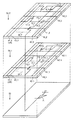
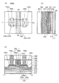
- FIG. 3 is a diagram illustrating a stacked configuration example of the photoelectric conversion element 21 and the holding circuit 32, and is a diagram illustrating a configuration example of a pixel included in the imaging device 10.
- n is set to 2 for the sake of clarity and the like and simplification of the description. That is, FIG. 3 illustrates the photoelectric conversion element 21, the holding circuit 32_1, and the holding circuit 32_2. In the following drawings and the like, n may be 2.
- the holding circuit 32_1 and the holding circuit 32_2 can have the same structure. Further, the holding circuits 32_1 to 32_n can have the same structure as each other; thus, the holding circuits 32_1 to 32_n can be manufactured using the same mask. Thereby, even if n is increased, it is possible to suppress an increase in the number of masks used when manufacturing the imaging device 10. That is, even if the number of layers 30 is increased, it is possible to suppress an increase in the number of masks used when manufacturing the imaging device 10. Therefore, even if the number of the layers 30 is increased, it is possible to suppress a large increase in the manufacturing cost of the imaging device 10, and to reduce the cost of the imaging device 10.
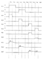
- FIG. 4 is a timing chart illustrating an example of an operation method of the imaging device 10 when the pixel has the configuration illustrated in FIG.
- H indicates a high potential
- L indicates a low potential.
- H indicates a high potential
- L indicates a low potential.
- all of the transistors 12 to 15 are n-channel transistors, but any or all of them may be p-channel transistors. Even in this case, the operation method illustrated in FIG. 4 can be referred to by appropriately switching the high potential and the low potential.
- the potential of the wiring 41_1 and the potential of the wiring 42_1 are set to high potentials.
- the potentials of the wiring 41_2, the wiring 42_2, the wiring 43_1, and the wiring 43_2 are low.
- the transistors 12_1 and 13_1 are turned on, and the charges accumulated in the photoelectric conversion element 21 and the node FD_1 are reset.
- the potential of the node FD_2 is reset to the potential VR (reset operation).
- the potential of the wiring 42_1 is set to a low potential. Accordingly, the transistor 13_1 is turned off, and the charge stored in the photoelectric conversion element 21 in accordance with the illuminance of light applied to the photoelectric conversion element 21 is transferred to the node FD_1. Therefore, the potential of the node FD_1 changes according to the illuminance of the light applied to the photoelectric conversion element 21 (exposure operation).
- the imaging device 10 acquires the imaging data, and the imaging data is written to the holding circuit 32_1. Specifically, one piece of imaging data is written to the holding circuit 32_1.
- imaging data written to the holding circuit 32_1 may be referred to as first imaging data.
- the potential of the wiring 41_1 is set to a low potential.
- the transistor 12_1 is turned off, the exposure operation ends, and the potential of the node FD_1 is held. That is, the imaging data is held in the holding circuit 32_1 (holding operation).
- the potential of the wiring 41_2 and the potential of the wiring 42_2 are set to high potentials. Accordingly, the transistor 12_2 and the transistor 13_2 are turned on, and the charges accumulated in the photoelectric conversion element 21 and the node FD_2 are reset. Therefore, the potential of the node FD_2 is reset to the potential VR (reset operation).
- the potential of the wiring 42_2 is set to a low potential. Accordingly, the transistor 13_2 is turned off, and the charge stored in the photoelectric conversion element 21 in accordance with the illuminance of the light applied to the photoelectric conversion element 21 is transferred to the node FD_2. Therefore, the potential of the node FD_2 changes in accordance with the illuminance of the light applied to the photoelectric conversion element 21 (exposure operation). As described above, the imaging device 10 acquires the imaging data, and the imaging data is written to the holding circuit 32_2.
- the potential of the wiring 41_2 is set to a low potential. Accordingly, the transistor 12_2 is turned off, the exposure operation ends, and the potential of the node FD_2 is held. That is, the imaging data is held in the holding circuit 32_2 (holding operation).
- the potential of the wiring 43_1 and the potential of the wiring 43_2 are set to high potentials. Accordingly, the transistor 15_1 and the transistor 15_2 are turned on, the potential of the wiring 40_1 becomes a potential corresponding to the potential of the node FD_1, and the potential of the wiring 40_2 becomes a potential corresponding to the potential of the node FD_2. That is, the imaging data held in the holding circuit 32_1 and the imaging data held in the holding circuit 32_2 are read (read operation).
- the imaging data read from the holding circuit 32_1 is converted into digital data by the AD conversion circuit 35_1 and output to the outside of the imaging device 10 as a signal OUT_1. Further, the imaging data read from the holding circuit 32_2 is converted into digital data by the AD conversion circuit 35_2, and output to the outside of the imaging device 10 as a signal OUT_2.
- a digital signal corresponding to imaging data read from the holding circuit 32_1 is described as a signal IS_1
- a digital signal corresponding to imaging data read from the holding circuit 32_2 is described as a signal IS_2. Shown. The same description may be given in other drawings.
- the potential of the wiring 43_1 and the potential of the wiring 43_2 are low. Accordingly, the transistor 15_1 and the transistor 15_2 are turned off, and the reading operation ends.
- the above is an example of the operation method of the imaging device 10.
- the imaging data held in the holding circuit 32_1 and the imaging data held in the holding circuit 32_2 are read.
- the imaging data held in the holding circuit 32_1 and the imaging data held in the holding circuit 32_2 are simultaneously read.
- n pieces of imaging data can be obtained at short time intervals without performing the reading at a high speed. This makes it possible to reduce the power consumption of the imaging device 10 while acquiring a plurality of imaging data at short time intervals.
- the holding circuits 32_1 to 32_n are provided so as to be stacked on each other. For this reason, even when n pieces of image data are read out collectively, image data corresponding to an image having the same resolution as that when reading out image data one by one can be obtained.
- the imaging apparatus 10 can achieve both acquisition of a plurality of pieces of imaging data at short time intervals and acquisition of imaging data corresponding to a high-resolution image.
- FIG. 5 is a block diagram illustrating a configuration example of the imaging device 10, which is a modification of FIG.
- the imaging device 10 illustrated in FIG. 1 includes a gate driver circuit 33, a source driver circuit 34, and an AD conversion circuit 35 provided in a layer 30.
- a gate driver circuit 33, a source driver circuit 34, and an AD conversion circuit 35 are provided in the layer 20.
- a demultiplexer circuit 36 and a multiplexer circuit 37 are provided on the layer 20 of the imaging device 10 having the configuration shown in FIG.
- the input terminal of the demultiplexer circuit 36 is electrically connected to the gate driver circuit 33.
- An output terminal of the demultiplexer circuit 36 is electrically connected to the holding circuit 32.
- the output terminal of the demultiplexer circuit 36 is electrically connected to the wirings 41 to 43 shown in FIG. From the above, it can be said that the demultiplexer circuit 36 is provided between the gate driver circuit 33 and the holding circuit 32.
- the input terminal of the multiplexer circuit 37 is electrically connected to the holding circuit 32 via the wiring 40.
- the output terminal of the multiplexer circuit 37 is electrically connected to the AD conversion circuit 35. From the above, it can be said that the multiplexer circuit 37 is provided between the holding circuit 32 and the AD conversion circuit 35.
- the number of the gate driver circuits 33, the number of the source driver circuits 34, and the number of the AD conversion circuits 35 are each reduced to less than n. Can be.
- one gate driver circuit 33, one source driver circuit 34, and one AD conversion circuit 35 can be provided in the layer 20.
- any or all of the gate driver circuit 33, the source driver circuit 34, and the AD conversion circuit 35 may be provided in the layer 20 two or more times.
- the imaging device 10 can have low power consumption.
- any one of the gate driver circuit 33, the source driver circuit 34, and the AD conversion circuit 35 may be provided in the layer 30.
- the gate driver circuit 33 may be provided in the layer 30 and the source driver circuit 34 and the AD conversion circuit 35 may be provided in the layer 20.
- the demultiplexer circuit 36 does not need to be provided in the imaging device 10.
- FIG. 6 is a timing chart illustrating an example of an operation method of the imaging device 10 when the pixels have the configuration illustrated in FIG. 3 and the imaging device 10 has the configuration illustrated in FIG.
- the operation in the period T11 to the period T16 illustrated in FIG. 6 is similar to the operation in the period T01 to the period T06 illustrated in FIG.
- the potential of the wiring 43_1 is set to a high potential. Accordingly, the transistor 15_1 is turned on, so that the potential of the wiring 40_1 becomes a potential corresponding to the potential of the node FD_1. That is, the imaging data held in the holding circuit 32_1 is read (read operation).
- the imaging data read from the holding circuit 32_1 is supplied to the AD conversion circuit 35 via the multiplexer circuit 37, and is converted into digital data by the AD conversion circuit 35.
- the digital data is output to the outside of the imaging device 10 as a signal OUT. That is, the signal IS_1 is output from the AD conversion circuit 35 to the outside of the imaging device 10.
- the potential of the wiring 43_1 is set to a low potential. Accordingly, the transistor 15_1 is turned off, and the operation of reading the imaging data held in the holding circuit 32_1 ends.
- the potential of the wiring 43_2 is set to a high potential. Accordingly, the transistor 15_2 is turned on, so that the potential of the wiring 40_2 becomes a potential corresponding to the potential of the node FD_2. That is, the imaging data held in the holding circuit 32_2 is read (read operation).
- the imaging data read from the holding circuit 32_2 is supplied to the AD conversion circuit 35 via the multiplexer circuit 37, and is converted into digital data by the AD conversion circuit 35.
- the digital data is output to the outside of the imaging device 10 as a signal OUT. That is, the signal IS_2 is output from the AD conversion circuit 35 to the outside of the imaging device 10.
- the potential of the wiring 43_2 is set to a low potential. Accordingly, the transistor 15_2 is turned off, and the operation of reading the imaging data held in the holding circuit 32_2 ends.
- the above is an example of the operation method of the imaging device 10.
- the imaging data held in the holding circuit 32_1 is read, and in the period T18, the imaging data held in the holding circuit 32_2 is read.
- the imaging data held in the holding circuit 32_1 and the imaging data held in the holding circuit 32_2 are sequentially read.
- the holding circuit 32 can hold the imaging data for a long time. Therefore, even when the image data is sequentially read, it is possible to suppress the image quality of the image corresponding to the read image data from deteriorating as compared with the case where the image data is read simultaneously.
- FIG. 7 is a block diagram illustrating a configuration example of the imaging device 10, which is a modification of FIG.
- the layer 30 including the holding circuit 32 is provided above the layer 20 including the photoelectric conversion element 21.
- the imaging device 10 having the configuration illustrated in FIG. 7 is different from the configuration illustrated in FIG. 1 in that a layer 30 having a holding circuit 32 is provided below the layer 20.
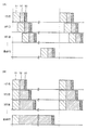
- FIGS. 8A and 8B are diagrams illustrating an operation method of a holding circuit 32 — i (i is an integer of 1 to n) provided in the imaging device 10 in a matrix. That is, FIGS. 8A and 8B are diagrams illustrating an operation method of the holding circuit 32 in a case where attention is paid to the holding circuits 32 provided in one layer 30 in a matrix.
- FIG. 8A is a diagram for explaining the operation of the rolling shutter system.
- the exposure operation 51, the holding operation 52, and the reading operation 53 are performed for each row of the holding circuit 32_i.
- FIG. 8B is a diagram for explaining the operation of the global shutter method.
- the exposure operation 51 is simultaneously performed on the holding circuits 32_i of all rows, and the reading operation 53 is sequentially performed for each row.
- the synchronization of imaging is lost, so that when the subject moves, the image is distorted.
- the global shutter method it is possible to secure the synchronization of imaging, and it is possible to easily obtain an image with small distortion even when the subject moves. Therefore, by using the global shutter method, the imaging device 10 can acquire imaging data corresponding to a high-quality image.
- the holding circuit 32 includes a transistor with an extremely low off-state current such as an OS transistor, the holding circuit 32 can hold imaging data for a long time. Therefore, a global shutter method can be used. As described above, the imaging device 10 can acquire imaging data corresponding to a high-quality image.
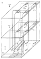
- FIG. 9 is a diagram illustrating a specific configuration example of a pixel included in the imaging device 10.
- FIG. 9 illustrates a cross-sectional configuration example of the photoelectric conversion element 21 and cross-sections in the channel length direction of the transistors 12_1, 13_1, 12_2, and 13_2. 2 shows a configuration example.
- the transistors 12 and 13 are OS transistors. Note that in some cases, some of the conductive layers and the insulating layers illustrated in the drawings are not provided, and in some cases, the conductive layers and the insulating layers that are not illustrated in the drawings are included in each layer.
- FIG. 9 a layer 30 is provided above the layer 20. Therefore, the configuration shown in FIG. 9 can be applied to, for example, the imaging apparatus 10 having the configuration shown in FIG.
- the photoelectric conversion element 21 is provided over the insulating layer 102.
- the insulating layer 102 for example, silicon oxide, silicon oxynitride, silicon nitride oxide, silicon nitride, aluminum oxide, aluminum oxynitride, aluminum nitride oxide, aluminum nitride, or the like can be used. Note that the same material as the insulating layer 102 can be used for the other insulating layers illustrated in FIGS.
- a two-terminal photodiode can be used.
- a pn photodiode using single crystal silicon a pin photodiode using an amorphous silicon thin film, a microcrystalline silicon thin film, a polycrystalline silicon thin film, or the like can be used.
- FIG. 9 illustrates a configuration example in which the photoelectric conversion element 21 is a pn-type photodiode using a single crystal silicon substrate.
- the photoelectric conversion element 21 having the structure illustrated in FIG. 9 can have a structure including the region 104, the region 106, the region 108, and the region 110.
- region 104 can be a p + region
- region 106 can be a p- region
- region 108 can be an n-type region
- region 110 can be a p + region.
- An insulating layer 112 is provided over the photoelectric conversion element 21, and an insulating layer 114 is provided over the insulating layer 112.
- the insulating layer 112 can function as a flattening film for flattening a step caused by the photoelectric conversion element 21 and the like provided thereunder.
- the upper surface of the insulating layer 112 may be planarized by a planarization process using a chemical mechanical polishing (CMP) method or the like to improve planarity.
- CMP chemical mechanical polishing
- a film having a barrier property such that hydrogen and other impurities are not diffused from the photoelectric conversion element 21 and the like to the transistors 12_1 to 15_1 provided in the holding circuit 32_1 is preferably used. Note that the transistor 14_1 and the transistor 15_1 are not illustrated in FIG.
- a film having a barrier property against hydrogen for example, silicon nitride formed by a chemical vapor deposition (CVD) method can be used.
- CVD chemical vapor deposition
- a film which suppresses diffusion of hydrogen is preferably used between the photoelectric conversion element 21 and the transistors 12_1 and 13_1.
- the film that suppresses the diffusion of hydrogen can be a film that releases a small amount of hydrogen.
- the amount of desorbed hydrogen can be analyzed by, for example, a thermal desorption gas analysis method (TDS: Thermal Desorption Spectroscopy).
- TDS Thermal Desorption Spectroscopy
- the desorbed amount of hydrogen in the insulating layer 114 is calculated by converting the desorbed amount into hydrogen atoms per area of the insulator 324. Therefore, it may be 10 ⁇ 10 15 atoms / cm 2 or less, preferably 5 ⁇ 10 15 atoms / cm 2 or less.
- the insulating layer 116_1 is provided over the insulating layer 114, and the transistor 12_1 and the transistor 13_1 are provided over the insulating layer 116_1.
- FIG. 10A is a cross-sectional view of a transistor 300 which can be used as the transistor 12 and the transistor 13 in a channel length direction
- FIG. 10B is a cross-sectional view of the transistor 300 in a channel width direction.
- the transistor 300 includes an insulating layer 118 provided over the insulating layer 116, an insulating layer 120 provided over the insulating layer 118, an insulating layer 122 provided over the insulating layer 120, A metal oxide 330a disposed thereon, a metal oxide 330b disposed on the metal oxide 330a, a conductive layer 342a and a conductive layer 342b disposed on the metal oxide 330b and separated from each other;
- An insulating layer 124 provided over the conductive layers 342a and 342b and having an opening formed so as to overlap between the conductive layers 342a and 342b; a conductive layer 360 provided in the openings; 330b, a conductive layer 342a, a conductive layer 342b, and
- the insulating layer 123 is provided between the metal oxide 330a, the metal oxide 330b, the conductive layer 342a, the conductive layer 342b, and the insulating layer 124.
- the conductive layer 360 includes a conductive layer 360a provided inside the insulating layer 350 and a conductive layer provided so as to be embedded inside the conductive layer 360a. 360b.
- the insulating layer 126 is preferably provided over the insulating layer 124, the conductive layer 360, and the insulating layer 350.
- the metal oxide 330a, the metal oxide 330b, and the metal oxide 330c may be collectively referred to as a metal oxide 330.
- the conductive layer 342a and the conductive layer 342b may be collectively referred to as a conductive layer 342.
- the transistor 300 a structure in which three layers of a metal oxide 330a, a metal oxide 330b, and a metal oxide 330c are stacked in a region where a channel is formed and in the vicinity thereof is shown; It is not limited to. For example, a single layer of the metal oxide 330b, a two-layer structure of the metal oxide 330b and the metal oxide 330a, a two-layer structure of the metal oxide 330b and the metal oxide 330c, or a stacked structure of four or more layers is provided. Is also good.
- the conductive layer 360 is illustrated as having a two-layer structure, but the present invention is not limited to this.
- the conductive layer 360 may have a single-layer structure or a stacked structure of three or more layers.
- the transistor 300 illustrated in FIGS. 10A and 10B is an example, and is not limited to this structure; an appropriate transistor may be used depending on a circuit configuration and a driving method.
- the conductive layer 360 functions as a gate of the transistor 300.
- the conductive layer 342a has a function as one of a source and a drain of the transistor 300
- the conductive layer 342b has a function as the other of the source and the drain of the transistor 300.
- the conductive layer 360 is formed so as to be buried in the opening of the insulating layer 124 and the region between the conductive layers 342a and 342b.
- the arrangement of the conductive layers 360, 342a, and 342b is selected in a self-aligned manner with respect to the opening of the insulating layer 124. That is, in the transistor 300, the gate can be arranged between the source and the drain in a self-aligned manner. Therefore, the conductive layer 360 can be formed without providing a positioning margin, so that the area occupied by the transistor 300 can be reduced. Thus, miniaturization and high integration of the imaging device can be achieved.
- the conductive layer 360 is formed in a self-aligned manner in a region between the conductive layer 342a and the conductive layer 342b, the conductive layer 360 does not have a region overlapping with the conductive layer 342a or the conductive layer 342b. Accordingly, parasitic capacitance formed between the conductive layer 360 and the conductive layers 342a and 342b can be reduced. Thus, the switching speed of the transistor 300 can be improved, and the frequency characteristics of the imaging device of one embodiment of the present invention can be improved.
- the insulating layer 350 has a function as a gate insulating film.
- an insulator containing more oxygen than oxygen that satisfies the stoichiometric composition is preferably used for the insulating layer 122 in contact with the metal oxide 330. That is, it is preferable that an excess oxygen region be formed in the insulating layer 122. By providing such an insulator containing excess oxygen in contact with the metal oxide 330, oxygen vacancies in the metal oxide 330 can be reduced and the reliability of the transistor 300 can be improved.
- an oxide material from which part of oxygen is released by heating as the insulator having an excess oxygen region.
- An oxide from which oxygen is released by heating means that the amount of desorbed oxygen converted to oxygen atoms by TDS analysis is 1.0 ⁇ 10 18 atoms / cm 3 or more, preferably 1.0 ⁇ 10 19 It is an oxide film having a thickness of at least atoms / cm 3 , more preferably at least 2.0 ⁇ 10 19 atoms / cm 3 or at least 3.0 ⁇ 10 20 atoms / cm 3 .
- the surface temperature of the film at the time of the TDS analysis is preferably in the range of 100 ° C to 700 ° C, or 100 ° C to 400 ° C.
- the insulating layer 120 preferably has a function of suppressing diffusion of oxygen (eg, an oxygen atom or an oxygen molecule) (the above-described oxygen is hardly transmitted).
- oxygen eg, an oxygen atom or an oxygen molecule
- the insulating layer 120 has a function of suppressing diffusion of oxygen and impurities, oxygen included in the metal oxide 330 does not diffuse to the insulating layer 118, which is preferable.
- the insulating layer 120 is formed of, for example, so-called high such as aluminum oxide, hafnium oxide, tantalum oxide, zirconium oxide, lead zirconate titanate (PZT), strontium titanate (SrTiO 3 ), or (Ba, Sr) TiO 3 (BST). It is preferable to use an insulator containing a -k material in a single layer or a stack. When a transistor is miniaturized and highly integrated, a problem such as a leak current may occur due to a reduction in thickness of a gate insulating film. With the use of a high-k material for an insulator having a function as a gate insulating film, reduction in gate potential at the time of transistor operation can be performed while the physical thickness is maintained.
- an insulator containing an oxide of one or both of aluminum and hafnium which is an insulating material having a function of suppressing diffusion of impurities and oxygen (the above oxygen is difficult to transmit), is preferably used.
- the insulator containing one or both oxides of aluminum and hafnium it is preferable to use aluminum oxide, hafnium oxide, an oxide containing aluminum and hafnium (hafnium aluminate), or the like.
- the insulating layer 120 serves to release oxygen from the metal oxide 330 and to mix impurities such as hydrogen from the periphery of the transistor 300 into the metal oxide 330. Has a function as a suppressing layer.
- aluminum oxide, bismuth oxide, germanium oxide, niobium oxide, silicon oxide, titanium oxide, tungsten oxide, yttrium oxide, or zirconium oxide may be added to these insulators.
- these insulators may be nitrided. Silicon oxide, silicon oxynitride, or silicon nitride may be stacked over the above insulator.
- the insulating layer 118 is preferably thermally stable.
- silicon oxide and silicon oxynitride are preferable because they are thermally stable.
- the insulating layer 118 having a stacked structure that is thermally stable and has a high relative dielectric constant can be obtained.
- the insulating layer 118, the insulating layer 120, and the insulating layer 122 may have a stacked structure of two or more layers.
- the structure is not limited to the laminated structure made of the same material, and may be a laminated structure made of different materials.
- a metal oxide having a function as an oxide semiconductor is preferably used for the metal oxide 330 including the channel formation region.
- an In-M-Zn oxide (element M is aluminum, gallium, yttrium, copper, vanadium, beryllium, boron, titanium, iron, nickel, germanium, zirconium, molybdenum, lanthanum, cerium, It is preferable to use a metal oxide such as neodymium, hafnium, tantalum, tungsten, magnesium, or one or more thereof.
- an In—Ga oxide or an In—Zn oxide may be used as the metal oxide 330.
- a metal oxide having a band gap of 2 eV or more, preferably 2.5 eV or more is preferably used as a metal oxide having a function as a channel formation region. With the use of a metal oxide having a large band gap as described above, the off-state current of the transistor can be reduced.
- the metal oxide 330 includes the metal oxide 330a below the metal oxide 330b, diffusion of impurities from a structure formed below the metal oxide 330a to the metal oxide 330b can be suppressed. it can. In addition, when the metal oxide 330c is provided over the metal oxide 330b, diffusion of impurities from the structure formed above the metal oxide 330c to the metal oxide 330b can be suppressed.
- the metal oxide 330 preferably has a stacked structure of metal oxides having different atomic ratios of metal atoms. Specifically, in the metal oxide used for the metal oxide 330a, the atomic ratio of the element M in the constituent elements is larger than that in the metal oxide used for the metal oxide 330b. , Preferably larger. In the metal oxide used for the metal oxide 330a, the atomic ratio of the element M to In is preferably larger than the atomic ratio of the element M to In in the metal oxide used for the metal oxide 330b. In the metal oxide used for the metal oxide 330b, the atomic ratio of In to the element M is preferably larger than that in the metal oxide used for the metal oxide 330a. As the metal oxide 330c, a metal oxide that can be used for the metal oxide 330a or the metal oxide 330b can be used.
- the energy of the lower end of the conduction band of the metal oxide 330a and the metal oxide 330c be higher than the energy of the lower end of the conduction band of the metal oxide 330b.
- the electron affinity of the metal oxide 330a and the metal oxide 330c be smaller than the electron affinity of the metal oxide 330b.
- the energy level at the bottom of the conduction band gradually changes.
- the energy level at the bottom of the conduction band at the junction of the metal oxide 330a, the metal oxide 330b, and the metal oxide 330c can be said to be continuously changed or continuously joined.
- the density of defect states in the mixed layer formed at the interface between the metal oxide 330a and the metal oxide 330b and the interface between the metal oxide 330b and the metal oxide 330c may be reduced.
- the metal oxide 330a and the metal oxide 330b and the metal oxide 330b and the metal oxide 330c have a common element other than oxygen (as a main component)
- a mixed state having a low defect state density is obtained.
- Layers can be formed.
- the metal oxide 330b is an In-Ga-Zn oxide
- an In-Ga-Zn oxide, a Ga-Zn oxide, gallium oxide, or the like may be used as the metal oxide 330a and the metal oxide 330c.
- the main path of the carrier is the metal oxide 330b.
- the density of defect states at the interface between the metal oxide 330a and the metal oxide 330b and the interface between the metal oxide 330b and the metal oxide 330c can be reduced. Can be lower. Therefore, the influence of interface scattering on carrier conduction is reduced, and the transistor 300 can have high on-state current.
- a conductive layer 342a serving as one of a source and a drain and a conductive layer 342b serving as the other of the source and the drain are provided over the metal oxide 330b.
- the conductive layer 342 aluminum, chromium, copper, silver, gold, platinum, tantalum, nickel, titanium, molybdenum, tungsten, hafnium, vanadium, niobium, manganese, magnesium, zirconium, beryllium, indium, ruthenium, iridium, strontium, It is preferable to use a metal element selected from lanthanum, an alloy containing the above-described metal element as a component, an alloy in which the above-described metal elements are combined, or the like.
- tantalum nitride, titanium nitride, tungsten, a nitride containing titanium and aluminum, a nitride containing tantalum and aluminum, ruthenium oxide, ruthenium nitride, an oxide containing strontium and ruthenium, an oxide containing lanthanum and nickel, and the like are used. Is preferred.
- tantalum nitride, titanium nitride, nitride containing titanium and aluminum, nitride containing tantalum and aluminum, ruthenium oxide, ruthenium nitride, oxide containing strontium and ruthenium, and oxide containing lanthanum and nickel are not easily oxidized.
- a conductive material or a material which maintains conductivity even when oxygen is absorbed is preferable.
- a region 343 (a region 343a and a region 343b) is formed as a low-resistance region in and near an interface of the metal oxide 330 with the conductive layer 342.
- the region 343a functions as one of the source region and the drain region
- the region 343b functions as the other of the source region and the drain region.
- a channel formation region is formed in a region between the region 343a and the region 343b.
- the oxygen concentration in the region 343 may be reduced in some cases. Further, in some cases, a metal compound layer containing a metal contained in the conductive layer 342 and a component of the metal oxide 330 is formed in the region 343. In such a case, the carrier density of the region 343 increases, and the region 343 becomes a low-resistance region.
- the insulating layer 123 is provided so as to cover the conductive layer 342, and suppresses oxidation of the conductive layer 342. At this time, the insulating layer 123 may be provided so as to cover a side surface of the metal oxide 330 and to be in contact with the insulating layer 122.
- a metal oxide containing one or two or more selected from hafnium, aluminum, gallium, yttrium, zirconium, tungsten, titanium, tantalum, nickel, germanium, or magnesium can be used. it can.
- the insulating layer 123 it is preferable to use aluminum oxide, hafnium oxide, an oxide containing aluminum and hafnium (hafnium aluminate), which is an insulator containing one or both of aluminum and hafnium.
- hafnium aluminate has higher heat resistance than a hafnium oxide film. Therefore, crystallization is difficult in a heat treatment in a subsequent step, which is preferable.
- the insulating layer 123 is not an essential component in the case where the conductive layer 342 has a material having oxidation resistance or does not have a significant decrease in conductivity even when it absorbs oxygen. An appropriate design may be made according to the required transistor characteristics.
- the insulating layer 350 has a function as a gate insulating film. It is preferable that the insulating layer 350 be disposed so as to be in contact with the inside (the upper surface and the side surface) of the metal oxide 330c.
- the insulating layer 350 is preferably formed using an insulator from which oxygen is released by heating.
- the amount of desorbed oxygen converted to oxygen atoms is 1.0 ⁇ 10 18 atoms / cm 3 or more, preferably 1.0 ⁇ 10 19 atoms / cm 3.
- the oxide film has a thickness of 3 cm 2 or more, more preferably 2.0 ⁇ 10 19 atoms / cm 3 or more, or 3.0 ⁇ 10 20 atoms / cm 3 or more.
- the surface temperature of the film at the time of the TDS analysis is preferably in the range of 100 ° C. or more and 700 ° C. or less.
- silicon oxide having excess oxygen silicon oxynitride, silicon nitride oxide, silicon nitride, silicon oxide added with fluorine, silicon oxide added with carbon, silicon oxide added with carbon and nitrogen, and holes are included. Silicon oxide can be used. In particular, silicon oxide and silicon oxynitride are preferable because they are stable against heat.
- the insulating layer 350 By providing an insulator from which oxygen is released by heating as an insulating layer 350 in contact with the upper surface of the metal oxide 330c, the insulating layer 350 has an effect on the channel formation region of the metal oxide 330b through the metal oxide 330c. Oxygen can be supplied. Further, similarly to the insulating layer 122, the concentration of impurities such as water or hydrogen in the insulating layer 350 is preferably reduced. The thickness of the insulating layer 350 is preferably greater than or equal to 1 nm and less than or equal to 20 nm.
- a metal oxide may be provided between the insulating layer 350 and the conductive layer 360.
- the metal oxide preferably suppresses oxygen diffusion from the insulating layer 350 to the conductive layer 360.
- diffusion of excess oxygen from the insulating layer 350 to the conductive layer 360 is suppressed. That is, a decrease in the amount of excess oxygen supplied to the metal oxide 330 can be suppressed. Further, oxidation of the conductive layer 360 due to excess oxygen can be suppressed.
- a material that can be used for the insulating layer 123 may be used.
- the conductive layer 360 serving as a gate has a two-layer structure in FIGS. 10A and 10B, but may have a single-layer structure or a stacked structure of three or more layers.
- the conductive layer 360a has a function of suppressing diffusion of impurities such as hydrogen atoms, hydrogen molecules, water molecules, nitrogen atoms, nitrogen molecules, nitrogen oxide molecules (N 2 O, NO, NO 2, and the like), and copper atoms. It is preferable to use a material. Alternatively, it is preferable to use a conductive material having a function of suppressing diffusion of oxygen (for example, at least one of oxygen atoms and oxygen molecules). When the conductive layer 360a has a function of suppressing diffusion of oxygen, it is possible to prevent the conductive layer 360b from being oxidized by oxygen contained in the insulating layer 350 and lowering the conductivity. As the conductive material having a function of suppressing diffusion of oxygen, for example, tantalum, tantalum nitride, ruthenium, ruthenium oxide, or the like is preferably used.
- the conductive layer 360b be formed using a conductive material mainly containing tungsten, copper, or aluminum.
- a conductor with high conductivity is preferably used.
- a conductive material containing tungsten, copper, or aluminum as a main component can be used.
- the conductive layer 360b may have a stacked structure, for example, a stacked structure of titanium, titanium nitride, and the above conductive material.
- the insulating layer 124 is provided over the conductive layer 342 with the insulating layer 123 interposed therebetween.
- the insulating layer 124 preferably has an excess oxygen region.
- silicon oxide and silicon oxynitride are preferable because they are thermally stable.
- silicon oxide and silicon oxide having holes are preferable because an excess oxygen region can be easily formed in a later step.
- the insulating layer 124 preferably has an excess oxygen region. By providing the insulating layer 124 from which oxygen is released by heating in contact with the metal oxide 330c, oxygen in the insulating layer 124 can be efficiently supplied to the metal oxide 330b through the metal oxide 330c. . Note that the concentration of impurities such as water or hydrogen in the insulating layer 124 is preferably reduced.
- the opening in the insulating layer 124 is formed to overlap with a region between the conductive layers 342a and 342b. Accordingly, the conductive layer 360 is formed so as to be embedded in the opening of the insulating layer 124 and in a region between the conductive layers 342a and 342b.
- the conductive layer 360 can have a shape with a high aspect ratio.
- the conductive layer 360 is provided so as to be embedded in the opening of the insulating layer 124, the conductive layer 360 can be formed without being collapsed during a process even when the conductive layer 360 has a high aspect ratio. Can be.
- the insulating layer 126 is preferably provided in contact with the upper surface of the insulating layer 124, the upper surface of the conductive layer 360, and the upper surface of the insulating layer 350.
- an excess oxygen region can be provided in the insulating layers 350 and 124.
- oxygen can be supplied into the metal oxide 330 from the excess oxygen region.
- a metal oxide containing one or two or more kinds selected from hafnium, aluminum, gallium, yttrium, zirconium, tungsten, titanium, tantalum, nickel, germanium, magnesium, or the like is used as the insulating layer 126.
- a metal oxide containing one or two or more kinds selected from hafnium, aluminum, gallium, yttrium, zirconium, tungsten, titanium, tantalum, nickel, germanium, magnesium, or the like is used as the insulating layer 126.
- hafnium, aluminum, gallium, yttrium, zirconium, tungsten, titanium, tantalum, nickel, germanium, magnesium, or the like is used as the insulating layer 126.
- aluminum oxide has a high barrier property and can suppress diffusion of hydrogen and nitrogen even in a thin film having a thickness of 0.5 nm or more and 3.0 nm or less. Therefore, aluminum oxide formed by a sputtering method can serve as an oxygen supply source and also have a function as a barrier film for impurities such as hydrogen.
- an insulating layer 128 having a function as an interlayer film is preferably provided over the insulating layer 126.
- the insulating layer 128 preferably has a reduced impurity concentration of water, hydrogen, or the like in the film.
- an opening reaching the conductive layer 202_1 and an opening reaching the conductive layer 204_1 are provided in the insulating layers 126_1 and 128_1, and the conductive layer 130_1 is provided so as to fill the openings.
- an opening portion reaching the conductive layer 206_1, an opening portion reaching the conductive layer 208_1, and an opening portion reaching the conductive layer 210_1 are provided in the insulating layer 123_1, the insulating layer 124_1, the insulating layer 126_1, and the insulating layer 128_1.
- the conductive layer 130_1 is provided so as to fill the portion.
- the conductive layers 202_1 and 204_1 correspond to the conductive layers 360 illustrated in FIGS. 10A and 10B
- the conductive layers 206_1, 208_1, and 210_1 correspond to the conductive layers illustrated in FIG. It corresponds to the layer 342a or the conductive layer 342b.
- the conductive layer 130 can have a two-layer structure of a conductive layer 130a and a conductive layer 130b as illustrated in FIG.
- a material of the conductive layers 130a and 130b a single layer or a stacked layer of a conductive material such as a metal material, an alloy material, a metal nitride material, or a metal oxide material can be used. It is preferable to use a high melting point material such as tungsten or molybdenum, which has both heat resistance and conductivity, and it is preferable to use tungsten. Alternatively, it is preferable to use a low-resistance conductive material such as aluminum or copper. By using a low-resistance conductive material, wiring resistance can be reduced. Note that the conductive layer 130 may have a single-layer structure or a stacked structure of three or more layers.
- the conductive layer 131, the conductive layer 132, the conductive layer 134, the conductive layer 136, the conductive layer 138, and the conductive layer 140 are provided so as to have a region in contact with the conductive layer 130_1.
- the region 108 and the conductive layer 206_1 are electrically connected to each other through the conductive layer 130_1 and the conductive layer 131.
- the conductive layer 132 is electrically connected to the conductive layer 202_1 through the conductive layer 130_1.
- the conductive layer 134 is electrically connected to the conductive layer 210_1 through the conductive layer 130_1.
- the conductive layer 136 is electrically connected to the conductive layer 204_1 through the conductive layer 130_1.
- the conductive layer 138 is electrically connected to the conductive layer 208_1 through the conductive layer 130_1.
- the conductive layer 140 is electrically connected to the region 110 through the conductive layer 130_1.
- the conductive layer 132 can be a part of the wiring 41_1 illustrated in FIG.
- the conductive layer 136 can be a part of the wiring 42_1 illustrated in FIG.
- the conductive layer 138 can be a part of the wiring 44_1 illustrated in FIG.
- the conductive layer 140 can be a part of the wiring 47 illustrated in FIG.
- an element selected from molybdenum, titanium, tantalum, tungsten, aluminum, copper, chromium, neodymium, and scandium is used.
- a metal film containing a metal, a metal nitride film containing the above-described element as a component can be used.
- indium tin oxide indium oxide containing tungsten oxide, indium zinc oxide containing tungsten oxide, indium oxide containing titanium oxide, indium tin oxide containing titanium oxide, indium zinc oxide, and silicon oxide are added.
- a conductive material such as indium tin oxide described above can also be used.
- the conductive layer 131, the conductive layer 132, the conductive layer 134, the conductive layer 136, the conductive layer 138, and the conductive layer 140 have a single-layer structure; however, the structure is not limited thereto and a stacked structure of two or more layers is used. May be.
- a conductor having a barrier property and a conductor having high adhesion to a conductor having a high conductivity may be formed between a conductor having a barrier property and a conductor having a high conductivity.
- An insulating layer 142 is provided over the insulating layer 128_1, the conductive layer 131, the conductive layer 132, the conductive layer 134, the conductive layer 136, the conductive layer 138, and the conductive layer 140.
- the insulating layer 142 can have a structure similar to that of the insulating layer 112.
- An insulating layer 144 is provided over the insulating layer 142.
- the insulating layer 144 can have a structure similar to that of the insulating layer 114. Accordingly, the insulating layer 144 can have a barrier property against hydrogen and the like, and can prevent deterioration in characteristics of the OS transistor provided in the layer 30_2.
- the insulating layer 116_2 is provided over the insulating layer 144, and the transistor 12_2 and the transistor 13_2 are provided over the insulating layer 116_2.
- the transistor 300 illustrated in FIGS. 10A and 10B can be used as the transistor 12_2 and the transistor 13_2.
- the transistors 12_1, 13_1, 12_2, and 13_2 can have the same structure.
- a conductive layer 202_2 and a conductive layer 204_2 correspond to the conductive layer 360 illustrated in FIGS. 10A and 10B, and a conductive layer 206_2, a conductive layer 208_2, and a conductive layer 210_2 are illustrated in FIG. It corresponds to the conductive layer 342a or the conductive layer 342b.
- the conductive layer 161, the conductive layer 162, the conductive layer 164, the conductive layer 166, the conductive layer 168, and the conductive layer 170 are provided so as to have a region in contact with the conductive layer 130_2.
- the region 108 and the conductive layer 206_2 are electrically connected to each other through the conductive layers 130_1, 131, 130_2, and 161.
- the conductive layer 162 is electrically connected to the conductive layer 202_2 through the conductive layer 130_2.
- the conductive layer 164 is electrically connected to the conductive layer 210_2 through the conductive layer 130_2.
- the conductive layer 166 is electrically connected to the conductive layer 204_2 through the conductive layer 130_2.
- the conductive layer 168 is electrically connected to the conductive layer 208_2 through the conductive layer 130_2.
- the conductive layer 170 is electrically connected to the region 110 through the conductive layers 130_2, 140, and 130_1.
- the conductive layer 162 can be a part of the wiring 41_2 illustrated in FIG.
- the conductive layer 166 can be a part of the wiring 42_2 illustrated in FIG.
- the conductive layer 168 can be a part of the wiring 44_2 illustrated in FIG.
- the conductive layer 170 can be a part of the wiring 47 illustrated in FIG.
- the conductive layer 161, the conductive layer 162, the conductive layer 164, the conductive layer 166, the conductive layer 168, and the conductive layer 170 are the conductive layer 131, the conductive layer 132, the conductive layer 134, the conductive layer 136, the conductive layer 138, and the conductive layer 140.
- the same configuration as that described above can be adopted.
- An insulating layer 172 is provided over the insulating layer 128_2, the conductive layer 161, the conductive layer 162, the conductive layer 164, the conductive layer 166, the conductive layer 168, and the conductive layer 170.
- the insulating layer 172 can have a structure similar to that of the insulating layer 112 and the insulating layer 142. The above is the description of the configuration example of the pixel included in the imaging device 10 having the configuration illustrated in FIG.
- the holding circuit 32_1 provided in the layer 30_1 and the holding circuit 32_2 provided in the layer 30_2 can have the same structure.
- the conductive layer 202_1 has a region overlapping with the conductive layer 202_2
- the conductive layer 204_1 has a region overlapping with the conductive layer 204_2
- the conductive layer 206_1 has a region overlapping with the conductive layer 206_2.
- the conductive layer 208_1 has a region overlapping with the conductive layer 208_2
- the conductive layer 210_1 can have a region overlapping with the conductive layer 210_2.
- the conductive layer 130_1 can have a region overlapping with the conductive layer 130_2.
- the conductive layer 131 has a region overlapping with the conductive layer 161
- the conductive layer 132 has a region overlapping with the conductive layer 162
- the conductive layer 134 has a region overlapping with the conductive layer 164
- the conductive layer 136 has a region overlapping with the conductive layer 164.
- the conductive layer 138 has a region overlapping with the conductive layer 168
- the conductive layer 138 has a region overlapping with the conductive layer 170.
- the imaging device of one embodiment of the present invention can achieve both acquisition of a plurality of pieces of imaging data at short time intervals and acquisition of imaging data corresponding to a high-quality image.
- the holding circuit 32_2 can be manufactured using the same mask as a mask used for manufacturing the holding circuit 32_1. Accordingly, it is possible to suppress the number of masks used when manufacturing the imaging device 10 from increasing more than when only one layer 30 is provided. Therefore, compared to the case where only one layer 30 is provided, the manufacturing cost of the imaging device 10 is prevented from increasing significantly, and the imaging device 10 can be made inexpensive.
- FIG. 11A is a diagram illustrating a specific configuration example of a pixel included in the imaging device 10 and is a modification example of the configuration illustrated in FIG.
- a layer 30 is provided below the layer 20. Therefore, the configuration illustrated in FIG. 11A can be applied to, for example, the imaging device 10 illustrated in FIG.
- the insulating layer 112 is provided over the substrate 100, the insulating layer 114 is provided over the insulating layer 112, and the layer 30 is provided over the insulating layer 114.
- the substrate 100 can be, for example, a substrate including silicon, for example, a single crystal silicon substrate.
- the insulating layer 173 is provided over the insulating layer 172.
- the insulating layer 173 can have a structure similar to that of the insulating layer 114 illustrated in FIG.
- the photoelectric conversion element 21 is provided over the insulating layer 173.
- the photoelectric conversion element 21 includes a conductive layer 176, a photoelectric conversion layer 182, and a conductive layer 184.
- the conductive layer 176 has a function as one electrode of the photoelectric conversion element 21, and the conductive layer 184 has a function as the other electrode of the photoelectric conversion element 21.
- An opening reaching the conductive layer 161 is provided in the insulating layers 173 and 172, and the conductive layer 176 can be formed so as to fill the opening.
- the conductive layer 176 can be formed so as to fill the opening.
- one of the source and the drain of the transistor 12 and one electrode of the photoelectric conversion element 21 are electrically connected.
- a conductive layer having a structure similar to that of the conductive layer 130 may be provided in the opening, and the conductive layer 176 may be provided so as to have a region in contact with the conductive layer.
- a conductive layer 178 is provided in the layer 20 so as to be separated from the conductive layer 176.
- the conductive layer 178 can be formed using the same material as the conductive layer 176 in the same step.
- the conductive layer 178 can be a part of the wiring 47 illustrated in FIG.
- the conductive layer 184 can be provided so as to have a region in contact with the conductive layer 178. Thereby, the other electrode of the photoelectric conversion element 21 and the wiring 47 can be electrically connected.
- the conductive layer 178 and the conductive layer 184 may not be in direct contact with each other but may be electrically connected to each other through another conductive layer.
- the photoelectric conversion layer 182 can have a structure including a selenium-based material.
- the photoelectric conversion element 21 using a selenium-based material has characteristics of high external quantum efficiency with respect to visible light.
- the selenium-based material has a high light absorption coefficient, and thus has an advantage that the photoelectric conversion layer 182 can be easily thinned.
- a high-sensitivity sensor with large amplification can be obtained by avalanche multiplication.
- a selenium-based material for the photoelectric conversion layer 182 a sufficient photocurrent can be obtained even when the pixel area is reduced, so that the imaging device 10 can have high sensitivity. Therefore, it can be said that the imaging device 10 provided with the photoelectric conversion element 21 using a selenium-based material is also suitable for imaging in a low illumination environment.
- amorphous selenium or crystalline selenium can be used as the selenium-based material.
- Crystalline selenium can be obtained, for example, by subjecting amorphous selenium to heat treatment after film formation. By making the crystal grain size of the crystalline selenium smaller than the pixel pitch, it is possible to reduce the variation in characteristics of each pixel.
- crystalline selenium has a higher spectral sensitivity to visible light and a higher light absorption coefficient than amorphous selenium.
- the photoelectric conversion layer 182 may be a layer containing a compound of copper, indium, and selenium (CIS).
- CIS copper, indium, and selenium
- CIGS copper, indium, gallium, and selenium
- a photoelectric conversion element utilizing avalanche multiplication can be formed in the same manner as with a single layer of selenium.
- the conductive layer 184 has a light-transmitting structure.
- the conductive layer 184 includes, for example, indium tin oxide, indium tin oxide containing silicon, indium oxide containing zinc, zinc oxide, zinc oxide containing gallium, zinc oxide containing aluminum, tin oxide containing tin, tin oxide containing fluorine, A structure including tin oxide containing antimony, graphene, graphene oxide, or the like can be employed.
- the conductive layer 184 is not limited to a single layer, and may be a stack of films including different materials.
- FIG. 11B is a cross-sectional view illustrating a configuration example of the photoelectric conversion element 21 in the case where an organic compound is used for the photoelectric conversion layer 182.
- a hole transport layer 186, an active layer 180, and an electron transport layer 188 are sequentially stacked on the photoelectric conversion layer 182.
- the conductive layer 178 has a function as an anode of the photoelectric conversion element 21, and the conductive layer 184 has a function as a cathode of the photoelectric conversion element 21. Note that when the conductive layer 178 has a function as a cathode of the photoelectric conversion element 21 and the conductive layer 184 has a function as an anode of the photoelectric conversion element 21, the stacking order is reversed.
- the active layer 180 has a function of absorbing light emitted to the photoelectric conversion element 21. Due to the photoelectric effect, a current according to the illuminance of the light absorbed by the active layer 180 flows through the photoelectric conversion element 21.
- the active layer 180 can have a structure in which a plurality of organic materials are appropriately combined.
- the active layer 180 can be configured to include tetraphenyldibenzoperiflanthene (DBP) and fullerene.
- DBP tetraphenyldibenzoperiflanthene
- the hole transporting layer 186 has a function of transporting holes from the conductive layer 178 having a function as an anode to the active layer 180.
- the hole transporting layer 186 includes a hole transporting material.
- the hole-transport layer 186 can have a structure including molybdenum oxide. Note that a material other than the above-described materials can be used for the hole-transport layer 186 as long as the hole-transport property is higher than the electron-transport property.
- the electron transport layer 188 has a function of transporting electrons from the conductive layer 184 having a function as a cathode to the active layer 180.
- the electron transporting layer 188 has an electron transporting material.
- the electron-transport layer 188 can have a single-layer structure or a stacked structure including two or more layers. For example, a stacked structure of fullerene and bathocuproine (BCP) can be used. Note that a material other than the above-described materials can be used for the electron-transport layer 188 as long as the material has a higher electron-transport property than the hole-transport property.
- the imaging device 10 can be made inexpensive. Further, the imaging device 10 can have flexibility.
- FIG. 12A is a perspective view illustrating an example in which a coloring layer (color filter) and the like are added to pixels included in the imaging device 10.
- a coloring layer color filter
- FIG. 12A is a perspective view illustrating an example in which a coloring layer (color filter) and the like are added to pixels included in the imaging device 10.
- An insulating layer 380 is formed on the layer 20 on which the photoelectric conversion element 21 is formed.
- a silicon oxide film or the like having high light-transmitting property with respect to visible light can be used.
- a silicon nitride film may be stacked as a passivation film.
- a dielectric film such as hafnium oxide may be laminated as an antireflection film.
- a light-blocking layer 381 may be formed over the insulating layer 380.
- the light-blocking layer 381 has a function of preventing color mixture of light passing through the upper coloring layer.
- a metal layer such as aluminum or tungsten can be used. Further, the metal layer and a dielectric film having a function as an antireflection film may be stacked.
- An organic resin layer 382 can be provided as a planarization film over the insulating layer 380 and the light-blocking layer 381. Further, a coloring layer 383 (a coloring layer 383a, a coloring layer 383b, and a coloring layer 383c) is formed for each pixel. For example, colors such as R (red), G (green), B (blue), Y (yellow), C (cyan), and M (magenta) are assigned to the coloring layers 383a, 383b, and 383c. Thus, a color image can be obtained.
- An insulating layer 386 having a property of transmitting visible light can be provided over the coloring layer 383.
- an optical conversion layer 385 may be used instead of the coloring layer 383.
- an imaging device that can obtain images in various wavelength regions can be provided.
- an infrared imaging device can be obtained.
- a filter that blocks light having a wavelength of near infrared rays or less is used for the optical conversion layer 385.
- a far-infrared imaging device can be obtained.
- an ultraviolet imaging device can be obtained.
- a colored layer corresponding to visible light and a filter corresponding to infrared light or ultraviolet light may be combined. With such a configuration, it is possible to detect a feature obtained from a combination of data of different wavelengths.
- a scintillator is used for the optical conversion layer 385, an imaging device that obtains an image in which the intensity of radiation used in an X-ray imaging device or the like is visualized can be obtained.
- radiation such as X-rays transmitted through a subject enters a scintillator, it is converted into light (fluorescence) such as visible light or ultraviolet light by a photoluminescence phenomenon. Then, image data is obtained by detecting the light with the photoelectric conversion element 21.
- the imaging device having the above configuration may be used for a radiation detector or the like.
- the scintillator includes a substance that, when irradiated with radiation such as X-rays or gamma rays, absorbs its energy and emits visible light or ultraviolet light.
- radiation such as X-rays or gamma rays
- Gd 2 O 2 S Tb
- Gd 2 O 2 S Pr
- Gd 2 O 2 S Eu
- BaFCl Eu
- NaI, CsI, CaF 2 , BaF 2 , CeF 3 LiF, LiI, ZnO, etc.
- Those dispersed in a resin or ceramics can be used.
- the photoelectric conversion element 21 using a selenium-based material radiation such as X-rays can be directly converted into electric charges, so that a structure in which a scintillator is unnecessary can be employed.
- a microlens array 384 may be provided over the coloring layer 383. Light passing through the individual lenses of the microlens array 384 passes through the coloring layer 383 immediately below and is irradiated on the photoelectric conversion element 21. Further, a microlens array 384 may be provided over the optical conversion layer 385 illustrated in FIG.
- FIG. 13A is a top view of the transistor 510A.
- FIG. 13B is a cross-sectional view of a portion indicated by a dashed-dotted line L1-L2 in FIG.
- FIG. 13C is a cross-sectional view of a part indicated by a dashed-dotted line W1-W2 in FIG. Note that for simplification of the drawing, some components are not illustrated in the top view in FIG.
- the insulating layer 574, the insulating layer 580, the insulating layer 582, and the insulating layer 584 are illustrated.
- a conductive layer 546 (a conductive layer 546a and a conductive layer 546b) which is electrically connected to the transistor 510A and has a function as a contact plug is illustrated.
- the transistor 510A includes an insulating layer 524 serving as a base insulating layer, a conductive layer 560 serving as a gate (conductive layers 560a and 560b), and an insulating layer 550 serving as a gate insulating film.
- a metal oxide 530 including a region where a channel is formed (a metal oxide 530a, a metal oxide 530b, and a metal oxide 530c); a conductive layer 542a serving as one of a source and a drain; And a conductive layer 542b having a function as the other.
- the metal oxide 530c, the insulating layer 550, and the conductive layer 560 are provided in an opening provided in the insulating layer 580 with the insulating layer 574 provided therebetween. Further, the metal oxide 530c, the insulating layer 550, and the conductive layer 560 are provided between the conductive layers 542a and 542b.
- the insulating layers 511 and 512 have a function as an interlayer film.
- An insulating layer such as TiO 3 (BST) can be used as a single layer or a stacked layer.
- aluminum oxide, bismuth oxide, germanium oxide, niobium oxide, silicon oxide, titanium oxide, tungsten oxide, yttrium oxide, or zirconium oxide may be added.
- these insulating layers may be subjected to a nitriding treatment. Silicon oxide, silicon oxynitride, or silicon nitride may be stacked over the above insulating layer.
- the insulating layer 511 preferably has a function as a barrier film for preventing impurities such as water or hydrogen from entering the transistor 510A from the substrate side. Therefore, it is preferable that the insulating layer 511 be formed using an insulating material having a function of suppressing diffusion of impurities such as hydrogen atoms, hydrogen molecules, water molecules, and copper atoms (the above impurities are hardly transmitted). Alternatively, it is preferable to use an insulating material which has a function of suppressing diffusion of oxygen (for example, at least one of an oxygen atom and an oxygen molecule) (the above oxygen is not easily transmitted). Further, for example, aluminum oxide, silicon nitride, or the like may be used for the insulating layer 511. With such a structure, diffusion of impurities such as hydrogen and water from the substrate side to the transistor 510A than the insulating layer 511 can be suppressed.
- the insulating layer 512 preferably has a lower dielectric constant than the insulating layer 511.
- parasitic capacitance generated between wirings can be reduced.
- the conductive layer 560 may have a function as a gate in some cases.
- the insulating layers 514 and 516 each have a function as an interlayer film, similarly to the insulating layers 511 and 512.
- the insulating layer 514 preferably has a function as a barrier film that prevents impurities such as water or hydrogen from entering the transistor 510A from the substrate side. With such a structure, diffusion of impurities such as hydrogen and water from the substrate side to the transistor 510A than the insulating layer 514 can be suppressed.
- the insulating layer 516 preferably has a lower dielectric constant than the insulating layer 514. By using a material having a low dielectric constant as an interlayer film, parasitic capacitance generated between wirings can be reduced.
- the insulating layer 522 preferably has a barrier property.
- the insulating layer 522 functions as a layer for preventing impurities such as hydrogen from entering the transistor 510A from the periphery of the transistor 510A.
- the insulating layer 522 is formed using, for example, aluminum oxide, hafnium oxide, an oxide containing aluminum and hafnium (hafnium aluminate), tantalum oxide, zirconium oxide, lead zirconate titanate (PZT), strontium titanate (SrTiO 3 ), or ( It is preferable that an insulating layer containing a so-called high-k material such as Ba, Sr) TiO 3 (BST) be used as a single layer or a stacked layer.
- a problem such as a leak current may occur due to a reduction in thickness of a gate insulating film.
- a high-k material is used for an insulating layer having a function as a gate insulating film, reduction in gate potential during transistor operation can be performed while the physical thickness is maintained.
- the insulating layer 521 is preferably, for example, thermally stable.
- the insulating layer 521 is formed using a high-k material and the insulating layer 522 is formed using a material containing silicon oxide and / or oxynitriding, so that the insulating layer 521 is thermally stable.
- a laminated structure having a high relative dielectric constant can be obtained.
- the metal oxide 530 having a region functioning as a channel formation region includes a metal oxide 530a, a metal oxide 530b over the metal oxide 530a, and a metal oxide 530c over the metal oxide 530b.
- a metal oxide 530a provided below the metal oxide 530b, diffusion of impurities from a structure formed below the metal oxide 530a to the metal oxide 530b can be suppressed.
- the metal oxide 530c is provided over the metal oxide 530b, diffusion of impurities from a structure formed above the metal oxide 530c to the metal oxide 530b can be suppressed.
- the metal oxide 530 an oxide semiconductor which is one of the above-described metal oxides can be used.
- the metal oxide 530 c is preferably provided in an opening provided in the insulating layer 580 with the insulating layer 574 interposed therebetween.
- the insulating layer 574 has a barrier property, diffusion of impurities from the insulating layer 580 to the metal oxide 530 can be suppressed.
- One of the conductive layers 542 functions as a source, and the other functions as a drain.
- a metal such as aluminum, titanium, chromium, nickel, copper, yttrium, zirconium, molybdenum, silver, tantalum, or tungsten, or an alloy containing this as a main component can be used.
- a metal nitride film such as tantalum nitride is preferable because it has a barrier property against hydrogen or oxygen and has high oxidation resistance.
- FIG. 13 shows a single-layer structure
- a stacked structure of two or more layers may be used.
- a tantalum nitride film and a tungsten film may be stacked.
- a titanium film and an aluminum film may be stacked.
- a two-layer structure in which an aluminum film is stacked on a tungsten film a two-layer structure in which a copper film is stacked on a copper-magnesium-aluminum alloy film, a two-layer structure in which a copper film is stacked on a titanium film, and A two-layer structure in which copper films are stacked may be used.
- a titanium film or a titanium nitride film a three-layer structure in which an aluminum film or a copper film is stacked over the titanium film or the titanium nitride film, and a titanium film or a titanium nitride film is further formed thereon, a molybdenum film or
- a molybdenum film or a three-layer structure in which a molybdenum nitride film, an aluminum film or a copper film are stacked over the molybdenum film or the molybdenum nitride film, and a molybdenum film or a molybdenum nitride film is formed thereover.
- a transparent conductive material containing indium oxide, tin oxide, or zinc oxide may be used.
- a barrier layer may be provided over the conductive layer 542.
- a substance having a barrier property to oxygen or hydrogen is preferably used. With this structure, oxidation of the conductive layer 542 can be suppressed when the insulating layer 574 is formed.
- a metal oxide can be used for the barrier layer.
- an insulating film having a barrier property against oxygen and hydrogen such as aluminum oxide, hafnium oxide, or gallium oxide.
- silicon nitride formed by a CVD method may be used.
- the range of selection of materials for the conductive layer 542 can be increased.
- a material having low oxidation resistance and high conductivity such as tungsten or aluminum can be used for the conductive layer 542.
- a conductive layer which can be easily formed or processed can be used.
- the insulating layer 550 has a function as a gate insulating film.
- the insulating layer 550 is preferably provided in an opening provided in the insulating layer 580 with the metal oxide 530c and the insulating layer 574 interposed therebetween.
- the insulating layer 550 may have a stacked structure.
- the insulating layer having a function as a gate insulating film has a stacked structure of a high-k material and a thermally stable material, so that the gate potential at the time of transistor operation is reduced while maintaining the physical film thickness. Becomes possible. Further, a laminated structure which is thermally stable and has a high relative dielectric constant can be obtained.
- the conductive layer 560 having a function as a gate includes a conductive layer 560a and a conductive layer 560b over the conductive layer 560a.
- the conductive layer 560a is preferably formed using a conductive material having a function of suppressing diffusion of impurities such as hydrogen atoms, hydrogen molecules, water molecules, and copper atoms.
- a conductive material having a function of suppressing diffusion of oxygen for example, at least one of oxygen atoms and oxygen molecules.
- the function of suppressing diffusion of impurities or oxygen means a function of suppressing diffusion of any one or all of the impurities or oxygen.
- the conductive layer 560a has a function of suppressing diffusion of oxygen, material selectivity of the conductive layer 560b can be improved. That is, by having the conductive layer 560a, even if a material that easily oxidizes is used as a material forming the conductive layer 560b, a decrease in conductivity due to oxidation of the conductive layer 560b can be suppressed.
- the conductive material having a function of suppressing diffusion of oxygen for example, tantalum, tantalum nitride, ruthenium, ruthenium oxide, or the like is preferably used.
- an oxide semiconductor that can be used as the metal oxide 530 can be used for the conductive layer 560a.
- the electric resistance of the conductive layer 560a can be reduced and the conductive layer 560b can be formed as a conductive layer. This can be called an OC (Oxide @ Conductor) electrode.
- the conductive layer 560b be formed using a conductive material mainly containing tungsten, copper, or aluminum.
- a conductive layer with high conductivity is preferably used.
- a conductive material containing tungsten, copper, or aluminum as a main component can be used.
- the conductive layer 560b may have a stacked structure, for example, a stacked structure of titanium, titanium nitride, and the above conductive material.
- An insulating layer 574 is provided between the insulating layer 580 and the transistor 510A.
- the insulating layer 574 is preferably formed using an insulating material having a function of suppressing diffusion of impurities such as water or hydrogen and oxygen.
- an insulating material having a function of suppressing diffusion of impurities such as water or hydrogen and oxygen.
- impurities such as water or hydrogen and oxygen.
- a metal oxide such as magnesium oxide, gallium oxide, germanium oxide, yttrium oxide, zirconium oxide, lanthanum oxide, neodymium oxide, or tantalum oxide, silicon nitride oxide, or silicon nitride can be used. .
- the imaging device of one embodiment of the present invention includes the insulating layer 574, impurities such as water and hydrogen included in the insulating layer 580 diffuse into the metal oxide 530b through the metal oxide 530c and the insulating layer 550. Can be suppressed. Further, oxidation of the conductive layer 560 due to excess oxygen included in the insulating layer 580 can be suppressed.
- the insulating layer 580, the insulating layer 582, and the insulating layer 584 have a function as an interlayer film.
- the insulating layer 582 preferably has a function as a barrier insulating film for preventing impurities such as water or hydrogen from entering the transistor 510A from the outside.
- the insulating layers 580 and 584 preferably have a lower dielectric constant than the insulating layer 582, similarly to the insulating layer 516.
- parasitic capacitance generated between wirings can be reduced.
- the transistor 510A may be electrically connected to another structure through a plug and a wiring such as the conductive layer 546 embedded in the insulating layer 580, the insulating layer 582, and the insulating layer 584.
- a conductive material such as a metal material, an alloy material, a metal nitride material, or a metal oxide material can be used as a single layer or a stacked layer.
- a high melting point material such as tungsten or molybdenum, which has both heat resistance and conductivity.
- a low-resistance conductive material such as aluminum or copper. By using a low-resistance conductive material, wiring resistance can be reduced.
- the conductive layer 546 has a stacked structure of, for example, tantalum nitride or the like, which is a conductive layer having a barrier property against hydrogen and oxygen, and tungsten, which has high conductivity, which maintains conductivity as a wiring. In this state, diffusion of impurities from the outside can be suppressed.
- the imaging device of one embodiment of the present invention has a metal oxide and a transistor with high on-state current. be able to.
- the imaging device of one embodiment of the present invention can be an imaging device including a transistor including a metal oxide and having a small off-state current.
- the imaging device of one embodiment of the present invention can be an imaging device in which fluctuation in electric characteristics is suppressed, stable electric characteristics are improved, and reliability is improved.
- FIG. 14A is a top view of the transistor 510B.
- FIG. 14B is a cross-sectional view of a part indicated by a dashed-dotted line L1-L2 in FIG.
- FIG. 14C is a cross-sectional view of a portion indicated by a dashed-dotted line W1-W2 in FIG. Note that for simplification of the drawing, some components are not illustrated in the top view in FIG.
- the transistor 510B is a modification example of the transistor 510A. Therefore, in order to prevent the description from being repeated, points different from the transistor 510A will be mainly described.
- the transistor 510B includes a region where the conductive layer 542 (the conductive layer 542a and the conductive layer 542b) overlaps with the metal oxide 530c, the insulating layer 550, and the conductive layer 560. With such a structure, a transistor with high on-state current can be provided. Further, a transistor with high controllability can be provided.
- the conductive layer 560 having a function as a gate includes a conductive layer 560a and a conductive layer 560b over the conductive layer 560a.
- the conductive layer 560a is preferably formed using a conductive material having a function of suppressing diffusion of impurities such as hydrogen atoms, hydrogen molecules, water molecules, and copper atoms.
- a conductive material having a function of suppressing diffusion of oxygen for example, at least one of oxygen atoms and oxygen molecules).
- the conductive layer 560a has a function of suppressing diffusion of oxygen, material selectivity of the conductive layer 560b can be improved. That is, by having the conductive layer 560a, oxidation of the conductive layer 560b can be suppressed, and a decrease in conductivity can be suppressed.
- the insulating layer 574 is preferably provided so as to cover the upper surface and the side surface of the conductive layer 560, the side surface of the insulating layer 550, and the side surface of the metal oxide 530c.
- the insulating layer 574 is preferably formed using an insulating material having a function of suppressing diffusion of impurities such as water or hydrogen and oxygen.
- an insulating material having a function of suppressing diffusion of impurities such as water or hydrogen and oxygen.
- a metal oxide such as magnesium oxide, gallium oxide, germanium oxide, yttrium oxide, zirconium oxide, lanthanum oxide, neodymium oxide, or tantalum oxide, silicon nitride oxide, or silicon nitride can be used. .
- oxidation of the conductive layer 560 can be suppressed.
- diffusion of impurities such as water and hydrogen included in the insulating layer 580 to the transistor 510B can be suppressed.
- an insulating layer 576 having a barrier property may be provided between the conductive layer 546 and the insulating layer 580.
- the provision of the insulating layer 576 can prevent oxygen in the insulating layer 580 from reacting with the conductive layer 546 and oxidizing the conductive layer 546.
- the insulating layer 576 having a barrier property a range of materials for a conductive layer used for a plug or a wiring can be increased.
- a metal material having a property of absorbing oxygen and having high conductivity for the conductive layer 546 an imaging device with low power consumption can be provided.
- a material having low oxidation resistance and high conductivity, such as tungsten or aluminum, can be used.
- a conductive layer which can be easily formed or processed can be used as the conductive layer 546.
- FIG. 15A is a top view of the transistor 510C.
- FIG. 15B is a cross-sectional view of a part indicated by a dashed-dotted line L1-L2 in FIG.
- FIG. 15C is a cross-sectional view of a part indicated by a dashed-dotted line W1-W2 in FIG. Note that for simplification of the drawing, some components are not illustrated in the top view in FIG.
- the transistor 510C is a modification example of the transistor 510A. Therefore, in order to prevent the description from being repeated, points different from the transistor 510A will be mainly described.
- a conductive layer 547a is provided between a conductive layer 542a and a metal oxide 530b, and a conductive layer 547b is provided between the conductive layer 542b and the metal oxide 530b.
- the conductive layer 542a extends beyond the upper surface of the conductive layer 547a (conductive layer 547b) and the side surface on the conductive layer 560 side, and has a region in contact with the upper surface of the metal oxide 530b.
- the conductive layer 547 a conductive layer which can be used for the conductive layer 542 may be used.
- the thickness of the conductive layer 547 is preferably larger than at least the conductive layer 542.
- the transistor 510C illustrated in FIG. 15 can have the conductive layer 542 closer to the conductive layer 560 than the transistor 510A.
- the conductive layer 560 can overlap with an end portion of the conductive layer 542a and an end portion of the conductive layer 542b. Accordingly, the substantial channel length of the transistor 510C can be reduced, and on-state current and frequency characteristics can be improved.
- the conductive layer 547a (the conductive layer 547b) is preferably provided so as to overlap with the conductive layer 542a (the conductive layer 542b).
- the conductive layer 547a (the conductive layer 547b) functions as a stopper and the metal oxide 530b is over-etched in the etching for forming the opening for filling the conductive layer 546a (the conductive layer 546b). Can be suppressed.
- the transistor 510C illustrated in FIG. 15 may have a structure in which the insulating layer 545 is provided in contact with the insulating layer 544.
- the insulating layer 544 preferably has a function as a barrier insulating film for preventing impurities such as water or hydrogen and excess oxygen from entering the transistor 510C from the insulating layer 580 side.
- an insulating layer which can be used for the insulating layer 544 can be used.
- a nitride insulating layer such as aluminum nitride, aluminum titanium nitride, titanium nitride, silicon nitride, or silicon nitride oxide may be used.
- FIG. 16A is a top view of the transistor 510D.
- FIG. 16B is a cross-sectional view of a part indicated by a dashed-dotted line L1-L2 in FIG.
- FIG. 16C is a cross-sectional view of a part indicated by a dashed-dotted line W1-W2 in FIG. Note that for simplification of the drawing, some components are not illustrated in the top view in FIG.
- the transistor 510D is a modification example of the above transistor. Therefore, in order to prevent repetition of the description, points different from the above transistors will be mainly described.
- the transistor 510D includes the insulating layer 550 over the metal oxide 530c and the metal oxide 552 over the insulating layer 550. Further, the conductive layer 560 is provided over the metal oxide 552 and the insulating layer 570 is provided over the conductive layer 560. Further, an insulating layer 571 is provided over the insulating layer 570.
- the metal oxide 552 preferably has a function of suppressing oxygen diffusion.
- the metal oxide 552 for suppressing diffusion of oxygen between the insulating layer 550 and the conductive layer 560, diffusion of oxygen to the conductive layer 560 is suppressed. That is, a decrease in the amount of oxygen supplied to the metal oxide 530 can be suppressed. Further, oxidation of the conductive layer 560 can be suppressed.
- the metal oxide 552 may have a function as part of the gate.
- an oxide semiconductor that can be used as the metal oxide 530 can be used as the metal oxide 552.
- the electric resistance of the metal oxide 552 can be reduced and the metal oxide 552 can be formed as a conductive layer. This can be called an OC (Oxide @ Conductor) electrode.
- the metal oxide 552 may have a function as part of the gate insulating film in some cases. Therefore, when silicon oxide or silicon oxynitride which is a material having high thermal stability is used for the insulating layer 550, it is preferable to use a metal oxide which is a high-k material having a high relative dielectric constant as the metal oxide 552. . With the stacked structure, the transistor 510D can be stable against heat and have a high relative dielectric constant. Therefore, it is possible to reduce the gate potential applied during the operation of the transistor while maintaining the physical film thickness. Further, the equivalent oxide thickness (EOT) of the insulating layer having a function as a gate insulating film can be reduced.
- EOT equivalent oxide thickness
- the metal oxide 552 is illustrated as a single layer; however, a stacked structure including two or more layers may be used. For example, a metal oxide having a function as part of a gate and a metal oxide having a function as part of a gate insulating film may be stacked.
- the on-state current of the transistor 510D can be improved without weakening the effect of an electric field from the conductive layer 560 in the case where the metal oxide 552 functions as a gate. .
- the distance between the conductive layer 560 and the metal oxide 530 can be kept by the physical thickness of the insulating layer 550 and the metal oxide 552. it can. Thus, leakage current between conductive layer 560 and metal oxide 530 can be suppressed.
- the transistor 510D has a stacked structure of the insulating layer 550 and the metal oxide 552, the physical distance between the conductive layer 560 and the metal oxide 530 and the distance from the conductive layer 560 to the metal oxide 530 are increased.
- the electric field strength can be easily and appropriately adjusted.
- the metal oxide 552 an oxide semiconductor which can be used for the metal oxide 530 and whose resistance is reduced can be used.
- a metal oxide containing one kind or two or more kinds selected from hafnium, aluminum, gallium, yttrium, zirconium, tungsten, titanium, tantalum, nickel, germanium, magnesium, or the like can be used.
- hafnium oxide an oxide containing aluminum and hafnium (hafnium aluminate), which is an insulating layer containing one or both of aluminum and hafnium.
- hafnium aluminate has higher heat resistance than a hafnium oxide film. Therefore, crystallization is difficult in a heat treatment in a subsequent step, which is preferable.
- the metal oxide 552 is not an essential component. An appropriate design may be made according to the required transistor characteristics.
- the insulating layer 570 is preferably formed using an insulating material having a function of suppressing transmission of impurities such as water or hydrogen and oxygen.
- an insulating material having a function of suppressing transmission of impurities such as water or hydrogen and oxygen.
- impurities such as water or hydrogen and oxygen.
- entry of impurities such as water or hydrogen into the metal oxide 530 from above the insulating layer 570 through the conductive layer 560 and the insulating layer 550 can be suppressed.
- the insulating layer 571 has a function as a hard mask.
- the side surface of the conductive layer 560 is substantially perpendicular to the substrate surface, specifically, the angle formed by the side surface of the conductive layer 560 and the substrate surface is 75 degrees.
- the angle can be not less than 100 degrees and preferably not less than 80 degrees and not more than 95 degrees.
- the insulating layer 571 may also serve as a barrier layer by using an insulating material having a function of suppressing transmission of impurities such as water or hydrogen and oxygen. In that case, the insulating layer 570 may not be provided.
- portions of the insulating layer 570, the conductive layer 560, the metal oxide 552, the insulating layer 550, and the metal oxide 530c are selectively removed so that their side surfaces substantially coincide with each other. Then, a part of the surface of the metal oxide 530b can be exposed.
- the transistor 510D includes a region 531a and a region 531b in part of the surface of the exposed metal oxide 530b.
- One of the region 531a and the region 531b functions as a source region, and the other of the region 531a and the region 531b has a function as a drain region.
- the regions 531a and 531b are formed by, for example, introducing an impurity element such as phosphorus or boron into the exposed surface of the metal oxide 530b by an ion implantation method, an ion doping method, a plasma immersion ion implantation method, plasma treatment, or the like. It can be realized by doing.
- the “impurity element” refers to an element other than the main component element.
- a metal film is formed after exposing a part of the surface of the metal oxide 530b, and then heat treatment is performed, so that an element included in the metal film is diffused into the metal oxide 530b and the region 531a and the region 531b can also be formed.
- the region 531a and the region 531b may be referred to as an “impurity region” or a “low-resistance region”.
- the region 531a and the region 531b can be formed in a self-aligned manner. Therefore, the conductive layer 560 does not overlap with the region 531a and / or the region 531b, so that parasitic capacitance can be reduced. Further, no offset region is formed between the channel formation region and the source / drain region (the region 531a or the region 531b).
- a self-aligned manner self-alignment
- an increase in on-state current, a reduction in threshold voltage, an increase in operation frequency, and the like can be realized.
- an offset region may be provided between the channel formation region and the source / drain region in order to further reduce the off-state current.
- the offset region is a region where the electric resistivity is high and where the above-described impurity element is not introduced.
- the formation of the offset region can be realized by introducing the above-described impurity element after the formation of the insulating layer 575.
- the insulating layer 575 also has a function as a mask similarly to the insulating layer 571 and the like. Therefore, an impurity element is not introduced into a region of the metal oxide 530b which overlaps with the insulating layer 575, so that the region can have high electric resistivity.
- the transistor 510D includes an insulating layer 570, a conductive layer 560, a metal oxide 552, an insulating layer 550, and an insulating layer 575 on a side surface of the metal oxide 530c.
- the insulating layer 575 is preferably an insulating layer having a low relative dielectric constant.
- silicon oxide, silicon oxynitride, silicon nitride oxide, or silicon oxide having holes for the insulating layer 575 because an excess oxygen region can be easily formed in the insulating layer 575 in a later step.
- silicon oxide and silicon oxynitride are preferable because they are thermally stable.
- the insulating layer 575 preferably has a function of diffusing oxygen.
- the transistor 510D includes an insulating layer 574 over the insulating layer 575 and the metal oxide 530.
- the insulating layer 574 is preferably formed by a sputtering method. By using a sputtering method, an insulating layer with less impurities such as water or hydrogen can be formed. For example, aluminum oxide may be used for the insulating layer 574.
- an oxide film formed by a sputtering method may extract hydrogen from a deposition target structure in some cases. Therefore, when the insulating layer 574 is formed by a sputtering method, the insulating layer 574 absorbs hydrogen and water from the metal oxide 530 and the insulating layer 575. Thus, the hydrogen concentrations of the metal oxide 530 and the insulating layer 575 can be reduced.
- FIG. 17A is a top view of the transistor 510E.
- FIG. 17B is a cross-sectional view of a part indicated by a dashed-dotted line L1-L2 in FIG.
- FIG. 17C is a cross-sectional view of a part indicated by a dashed-dotted line W1-W2 in FIG. Note that for simplification of the drawing, some components are not illustrated in the top view in FIG.
- the transistor 510E is a modification of the above transistor. Therefore, in order to prevent repetition of the description, points different from the above transistors will be mainly described.
- the transistor 510E does not include the conductive layer 542 and includes a region 531a and a region 531b over part of the surface of the exposed metal oxide 530b.
- One of the region 531a and the region 531b functions as a source region, and the other has a function as a drain region.
- an insulating layer 573 is provided between the metal oxide 530b and the insulating layer 574.
- a region 531 (a region 531a and a region 531b) illustrated in FIG. 17 is a region in which the following element is added to the metal oxide 530b.
- the region 531 can be formed by using, for example, a dummy gate.
- a dummy gate may be provided over the metal oxide 530b, and an element which reduces the resistance of the metal oxide 530b may be added using the dummy gate as a mask. That is, the element is added to a region where the metal oxide 530 does not overlap with the dummy gate, so that a region 531 is formed.
- the method for adding the element include an ion implantation method in which an ionized source gas is added by mass separation, an ion doping method in which an ionized source gas is added without mass separation, a plasma immersion ion implantation method, and the like. Can be used.
- boron or phosphorus is typically given.
- hydrogen, carbon, nitrogen, fluorine, sulfur, chlorine, titanium, a rare gas, or the like may be used.
- the rare gas include helium, neon, argon, krypton, and xenon.
- the concentration of the element may be measured using secondary ion mass spectrometry (SIMS: Secondary Ion Mass Spectrometry) or the like.
- boron and phosphorus are preferable because an apparatus of a production line for amorphous silicon or low-temperature polysilicon can be used. Existing equipment can be diverted and equipment investment can be reduced.
- an insulating film to be the insulating layer 573 and an insulating film to be the insulating layer 574 may be formed over the metal oxide 530b and the dummy gate.
- the insulating film to be the insulating layer 580 is subjected to a CMP (Chemical Mechanical Polishing) process, so that the insulating layer 580 and the insulating layer 580 are formed. A part of the insulating film is removed to expose the dummy gate. Subsequently, when removing the dummy gate, a part of the insulating layer 573 which is in contact with the dummy gate may be removed.
- CMP Chemical Mechanical Polishing
- the insulating layer 574 and the insulating layer 573 are exposed on the side surface of the opening provided in the insulating layer 580, and a part of the region 531 provided in the metal oxide 530b is provided on the bottom of the opening. Exposed.
- a CMP process or the like is performed until the insulating layer 580 is exposed. 17 can be formed by removing part of the oxide film to be the metal oxide 530c, the insulating film to be the insulating layer 550, and part of the conductive film to be the conductive layer 560.
- insulating layers 573 and 574 are not essential components. An appropriate design may be made according to the required transistor characteristics.
- an existing device can be used and the conductive layer 542 is not provided; thus, cost can be reduced.
- FIG. 18A1 is an external perspective view of the top surface side of a package containing an image sensor chip.
- the package includes a package substrate 610 for fixing the image sensor chip 650 illustrated in FIG. 18A3, a cover glass 620, an adhesive 630 for bonding the two, and the like.
- FIG. 18A2 is an external perspective view of the lower surface side of the package.
- a BGA Bit Grid Array
- LGA Land Grid Array
- PGA Peripheral Component Interconnect
- FIG. 18 (A3) is a perspective view of the package in which the cover glass 620 and a part of the adhesive 630 are omitted.
- An electrode pad 660 is formed over the package substrate 610, and the electrode pad 660 and the bump 640 illustrated in FIG. 18A2 are electrically connected via a through hole.
- the electrode pad 660 is electrically connected to the image sensor chip 650 via a wire 670.
- FIG. 18B1 is an external perspective view of the upper surface side of the camera module in which the image sensor chip is housed in a lens-integrated package.
- the camera module includes a package substrate 611 for fixing the image sensor chip 651 illustrated in FIG. 18B3, a lens cover 621, a lens 635, and the like.
- FIG. 18B2 is an external perspective view of the lower surface side of the camera module.
- a QFN Quad Flat No-lead package
- a mounting land 641 provided on the lower surface and side surfaces of the package substrate 611. Note that this configuration is an example, and a QFP (Quad Flat Package) or the aforementioned BGA may be provided.
- FIG. 18 (B3) is a perspective view of the module with a part of the lens cover 621 and the lens 635 omitted.
- the land 641 is electrically connected to the electrode pad 661, and the electrode pad 661 is electrically connected to the image sensor chip 651 or the IC chip 690 via the wire 671.
- An IC chip 690 having functions such as a driving circuit and a signal conversion circuit of an imaging device is also provided between the package substrate 611 and the image sensor chip 651, and has a configuration as a SiP (System @ in ⁇ Package). are doing.
- the image sensor chip By mounting the image sensor chip in the above-described package, mounting on a printed circuit board or the like is facilitated, and the image sensor chip can be incorporated in various semiconductor devices and electronic devices.
- FIG. 19A is a diagram illustrating the appearance of the camera 1000 with the viewfinder 1100 attached.
- the camera 1000 can be, for example, a digital camera.
- the camera 1000 and the finder 1100 are separate electronic devices and are configured to be detachable.
- a finder including a display device is incorporated in the housing 1001 of the camera 1000. Is also good.
- the camera 1000 includes a housing 1001, a display portion 1002, operation buttons 1003, a shutter button 1004, and the like.
- a detachable lens 1006 is attached to the camera 1000.
- the camera 1000 has a configuration in which the lens 1006 can be removed from the housing 1001 and replaced, but the lens 1006 and the housing may be integrated.
- the camera 1000 can capture an image by pressing a shutter button 1004. Further, the display portion 1002 has a function as a touch panel, and imaging can be performed by touching the display portion 1002.
- the housing 1001 of the camera 1000 has a mount having electrodes, and can connect a flash device or the like in addition to the finder 1100.
- the finder 1100 includes a housing 1101, a display portion 1102, and the like.
- Viewfinder 1100 can be an electronic viewfinder.
- the housing 1101 has a mount that engages with the mount of the camera 1000, and the finder 1100 can be attached to the camera 1000.
- the mount has electrodes, and an image or the like received from the camera 1000 via the electrodes can be displayed on the display portion 1102.
- the camera 1000 can include the imaging device of one embodiment of the present invention.
- the camera 1000 can acquire imaging data corresponding to a high-resolution image at short time intervals. Therefore, the camera 1000 can be a high-speed camera.
- FIG. 19B is a diagram illustrating an appearance of the head mounted display 1200.
- the head mounted display 1200 includes a mounting unit 1201, a lens 1202, a main body 1203, a display unit 1204, a cable 1205, and the like. Further, a battery 1206 is built in the mounting portion 1201.
- the cable 1205 supplies power from the battery 1206 to the main body 1203.
- the main body 1203 includes a wireless receiver or the like, and can display an image corresponding to received image data or the like on the display portion 1204.
- a camera provided in the main body 1203 to capture the movement of the user's eyeballs and eyelids and calculating the coordinates of the user's line of sight based on the information, the user's line of sight can be used as input means. it can.
- the mounting portion 1201 may be provided with a plurality of electrodes at positions where the electrodes touch the user.
- the main body 1203 may have a function of recognizing the user's line of sight by detecting a current flowing through the electrode in accordance with the movement of the user's eyeball. Further, a function of monitoring a pulse of the user by detecting a current flowing through the electrode may be provided.
- the mounting section 1201 may include various sensors such as a temperature sensor, a pressure sensor, and an acceleration sensor, and may have a function of displaying biological information of the user on the display section 1204. Further, the movement of the user's head or the like may be detected, and the image displayed on the display unit 1204 may be changed in accordance with the movement.
- the imaging device of one embodiment of the present invention can be provided.
- the camera can acquire imaging data corresponding to a high-resolution image at short time intervals. Therefore, the camera can be a high-speed camera.
- FIGS. 19C, 19D, and 19E are views showing the appearance of the head mounted display 1300.
- the head mounted display 1300 includes a housing 1301, a display unit 1302, a band-like fixing tool 1304, and a pair of lenses 1305.
- the user can visually recognize the display on the display unit 1302 through the lens 1305.
- the display portion 1302 be arranged in a curved manner. By arranging the display unit 1302 in a curved manner, the user can feel a high sense of realism.
- a configuration in which one display portion 1302 is provided is described in this embodiment, the present invention is not limited to this.
- a configuration in which two display portions 1302 are provided may be employed. In this case, if one display unit is arranged in one eye of the user, three-dimensional display using parallax can be performed.
- the head mounted display 1300 can be provided with a camera. Thereby, an outside scene can be imaged. Therefore, the head mounted display 1300 can combine a virtual image such as computer graphics (CG) with an image captured by the camera. Therefore, the head mounted display 1300 can be an augmented reality (Augmented Reality: AR) device.
- CG computer graphics
- AR Augmented Reality
- the imaging device of one embodiment of the present invention can be provided as the camera.
- the camera can acquire imaging data corresponding to a high-resolution image at short time intervals. Therefore, the camera can be a high-speed camera.
- FIG. 20A illustrates an appearance of a mobile phone 1400.
- the mobile phone 1400 includes a housing 1481, a display portion 1482, operation buttons 1483, an external connection port 1484, a speaker 1485, a microphone 1486, a camera 1487, and the like.
- This mobile phone includes a touch sensor in the display portion 1482. All operations such as making a call and inputting characters can be performed by touching the display portion 1482 with a finger, a stylus, or the like.
- the imaging device of one embodiment of the present invention can be provided as the camera 1487. Accordingly, the camera 1487 can acquire imaging data corresponding to a high-resolution image at short time intervals. Therefore, the camera 1487 can be a high-speed camera.
- FIG. 20B is a diagram illustrating an appearance of the portable data terminal 1500.
- the portable data terminal 1500 includes a housing 1511, a display unit 1512, a speaker 1513, a camera 1519, and the like. Information can be input and output by a touch panel function of the display portion 1512. In addition, a character or the like can be recognized from an image acquired by the camera 1519, and the character can be output as sound using the speaker 1513.
- the imaging device of one embodiment of the present invention can be provided as the camera 1519. Accordingly, the camera 1519 can acquire imaging data corresponding to a high-resolution image at short time intervals. Therefore, the camera 1519 can be a high-speed camera.
- FIG. 20C is a diagram illustrating an appearance of the monitoring camera 1600.
- Surveillance camera 1600 includes support base 1651, camera unit 1652, protective cover 1653, and the like.
- the camera unit 1652 is provided with a rotation mechanism and the like, and can be taken on the entire periphery by being installed on the ceiling.
- the surveillance camera is a conventional name and does not limit the use.
- a device having a function as a surveillance camera is also called a camera or a video camera.
- the imaging device of one embodiment of the present invention can be provided as the camera unit 1652. Accordingly, the camera unit 1652 can acquire imaging data corresponding to a high-resolution image at short time intervals. Therefore, the camera unit 1652 can be a high-speed camera.
- FIG. 20D illustrates an appearance of a wristwatch-type information terminal 1700.
- the information terminal 1700 includes a display portion 1732, a housing / wristband 1733, a camera 1739, and the like.
- the display unit 1732 includes a touch panel for operating an information terminal.
- the display portion 1732 and the housing / wristband 1733 have flexibility and are excellent in attachment to the body.
- the imaging device of one embodiment of the present invention can be provided as the camera 1739. Accordingly, the camera 1739 can acquire imaging data corresponding to a high-resolution image at short time intervals. Therefore, the camera 1739 can be a high-speed camera.
Landscapes
- Engineering & Computer Science (AREA)
- Multimedia (AREA)
- Signal Processing (AREA)
- Solid State Image Pick-Up Elements (AREA)
- Thin Film Transistor (AREA)
- Transforming Light Signals Into Electric Signals (AREA)
Priority Applications (5)
| Application Number | Priority Date | Filing Date | Title |
|---|---|---|---|
| CN201980035037.9A CN112189261B (zh) | 2018-06-21 | 2019-06-11 | 摄像装置及其工作方法以及电子设备 |
| US17/057,526 US11600645B2 (en) | 2018-06-21 | 2019-06-11 | Imaging device, operation method thereof, and electronic device |
| KR1020207035645A KR102769490B1 (ko) | 2018-06-21 | 2019-06-11 | 촬상 장치 및 그 동작 방법, 및 전자 기기 |
| JP2020524943A JP7221286B2 (ja) | 2018-06-21 | 2019-06-11 | 撮像装置及びその動作方法、並びに電子機器 |
| US18/117,784 US11862649B2 (en) | 2018-06-21 | 2023-03-06 | Imaging device, operation method thereof, and electronic device |
Applications Claiming Priority (2)
| Application Number | Priority Date | Filing Date | Title |
|---|---|---|---|
| JP2018117769 | 2018-06-21 | ||
| JP2018-117769 | 2018-06-21 |
Related Child Applications (2)
| Application Number | Title | Priority Date | Filing Date |
|---|---|---|---|
| US17/057,526 A-371-Of-International US11600645B2 (en) | 2018-06-21 | 2019-06-11 | Imaging device, operation method thereof, and electronic device |
| US18/117,784 Division US11862649B2 (en) | 2018-06-21 | 2023-03-06 | Imaging device, operation method thereof, and electronic device |
Publications (1)
| Publication Number | Publication Date |
|---|---|
| WO2019243951A1 true WO2019243951A1 (ja) | 2019-12-26 |
Family
ID=68983795
Family Applications (1)
| Application Number | Title | Priority Date | Filing Date |
|---|---|---|---|
| PCT/IB2019/054838 Ceased WO2019243951A1 (ja) | 2018-06-21 | 2019-06-11 | 撮像装置及びその動作方法、並びに電子機器 |
Country Status (5)
| Country | Link |
|---|---|
| US (2) | US11600645B2 (https=) |
| JP (1) | JP7221286B2 (https=) |
| KR (1) | KR102769490B1 (https=) |
| CN (1) | CN112189261B (https=) |
| WO (1) | WO2019243951A1 (https=) |
Families Citing this family (5)
| Publication number | Priority date | Publication date | Assignee | Title |
|---|---|---|---|---|
| TW202035577A (zh) * | 2018-09-06 | 2020-10-01 | 日商富士軟片股份有限公司 | 結構體、光感測器及圖像顯示裝置 |
| JP7526163B2 (ja) | 2019-07-26 | 2024-07-31 | 株式会社半導体エネルギー研究所 | 複合デバイス |
| WO2021140404A1 (ja) | 2020-01-10 | 2021-07-15 | 株式会社半導体エネルギー研究所 | 電子機器、及びプログラム |
| KR20220142457A (ko) | 2020-02-20 | 2022-10-21 | 가부시키가이샤 한도오따이 에네루기 켄큐쇼 | 촬상 장치, 전자 기기, 및 이동체 |
| JP2024130238A (ja) * | 2023-03-14 | 2024-09-30 | 株式会社東芝 | イメージセンサおよびイメージセンサモジュール |
Citations (4)
| Publication number | Priority date | Publication date | Assignee | Title |
|---|---|---|---|---|
| JP2014072418A (ja) * | 2012-09-28 | 2014-04-21 | Sony Corp | 半導体装置、固体撮像装置、および半導体装置の製造方法 |
| JP2016213298A (ja) * | 2015-05-07 | 2016-12-15 | 株式会社半導体エネルギー研究所 | 撮像装置および電子機器 |
| JP2017063420A (ja) * | 2015-09-25 | 2017-03-30 | 株式会社半導体エネルギー研究所 | 半導体装置 |
| WO2017169480A1 (ja) * | 2016-03-31 | 2017-10-05 | 株式会社ニコン | 撮像素子および撮像装置 |
Family Cites Families (16)
| Publication number | Priority date | Publication date | Assignee | Title |
|---|---|---|---|---|
| CN104393007A (zh) | 2009-11-06 | 2015-03-04 | 株式会社半导体能源研究所 | 半导体装置 |
| JP5505709B2 (ja) * | 2010-03-31 | 2014-05-28 | ソニー株式会社 | 固体撮像素子およびその製造方法、並びに電子機器 |
| JP5791571B2 (ja) * | 2011-08-02 | 2015-10-07 | キヤノン株式会社 | 撮像素子及び撮像装置 |
| CN103208501B (zh) * | 2012-01-17 | 2017-07-28 | 奥林巴斯株式会社 | 固体摄像装置及其制造方法、摄像装置、基板、半导体装置 |
| KR102450562B1 (ko) | 2014-03-13 | 2022-10-07 | 가부시키가이샤 한도오따이 에네루기 켄큐쇼 | 촬상 장치 |
| TWI656631B (zh) | 2014-03-28 | 2019-04-11 | 日商半導體能源研究所股份有限公司 | 攝像裝置 |
| US11309284B2 (en) | 2014-10-06 | 2022-04-19 | Sony Corporation | Solid-state image capturing apparatus and electronic device for acquiring a normal image and a narrow band image |
| JP6570417B2 (ja) | 2014-10-24 | 2019-09-04 | 株式会社半導体エネルギー研究所 | 撮像装置および電子機器 |
| US9773832B2 (en) | 2014-12-10 | 2017-09-26 | Semiconductor Energy Laboratory Co., Ltd. | Semiconductor device and electronic device |
| JP6502597B2 (ja) * | 2015-04-16 | 2019-04-17 | 株式会社半導体エネルギー研究所 | 撮像装置 |
| US10090344B2 (en) | 2015-09-07 | 2018-10-02 | Semiconductor Energy Laboratory Co., Ltd. | Imaging device, method for operating the same, module, and electronic device |
| US10896923B2 (en) * | 2015-09-18 | 2021-01-19 | Semiconductor Energy Laboratory Co., Ltd. | Method of operating an imaging device with global shutter system |
| CN108140657A (zh) | 2015-09-30 | 2018-06-08 | 株式会社半导体能源研究所 | 半导体装置及电子设备 |
| JP2017108066A (ja) * | 2015-12-11 | 2017-06-15 | 株式会社東芝 | 撮像装置、撮像システム及び撮像装置の駆動方法 |
| JP2018011162A (ja) * | 2016-07-13 | 2018-01-18 | ソニー株式会社 | 固体撮像素子、撮像装置、および、固体撮像素子の制御方法 |
| CN113660439A (zh) | 2016-12-27 | 2021-11-16 | 株式会社半导体能源研究所 | 摄像装置及电子设备 |
-
2019
- 2019-06-11 CN CN201980035037.9A patent/CN112189261B/zh active Active
- 2019-06-11 US US17/057,526 patent/US11600645B2/en active Active
- 2019-06-11 JP JP2020524943A patent/JP7221286B2/ja active Active
- 2019-06-11 WO PCT/IB2019/054838 patent/WO2019243951A1/ja not_active Ceased
- 2019-06-11 KR KR1020207035645A patent/KR102769490B1/ko active Active
-
2023
- 2023-03-06 US US18/117,784 patent/US11862649B2/en active Active
Patent Citations (4)
| Publication number | Priority date | Publication date | Assignee | Title |
|---|---|---|---|---|
| JP2014072418A (ja) * | 2012-09-28 | 2014-04-21 | Sony Corp | 半導体装置、固体撮像装置、および半導体装置の製造方法 |
| JP2016213298A (ja) * | 2015-05-07 | 2016-12-15 | 株式会社半導体エネルギー研究所 | 撮像装置および電子機器 |
| JP2017063420A (ja) * | 2015-09-25 | 2017-03-30 | 株式会社半導体エネルギー研究所 | 半導体装置 |
| WO2017169480A1 (ja) * | 2016-03-31 | 2017-10-05 | 株式会社ニコン | 撮像素子および撮像装置 |
Also Published As
| Publication number | Publication date |
|---|---|
| US20230207585A1 (en) | 2023-06-29 |
| JPWO2019243951A1 (ja) | 2021-07-08 |
| US11600645B2 (en) | 2023-03-07 |
| CN112189261A (zh) | 2021-01-05 |
| KR102769490B1 (ko) | 2025-02-17 |
| KR20210021463A (ko) | 2021-02-26 |
| US11862649B2 (en) | 2024-01-02 |
| JP7221286B2 (ja) | 2023-02-13 |
| CN112189261B (zh) | 2025-01-28 |
| US20210202549A1 (en) | 2021-07-01 |
Similar Documents
| Publication | Publication Date | Title |
|---|---|---|
| US12165049B2 (en) | Imaging device, imaging module, electronic device, and imaging system | |
| JP7221286B2 (ja) | 撮像装置及びその動作方法、並びに電子機器 | |
| CN108604592B (zh) | 半导体装置、半导体装置的制造方法、固态成像装置以及电子设备 | |
| JP7185744B2 (ja) | 撮像装置 | |
| CN107040731A (zh) | 摄像装置、模块、电子设备及摄像装置的工作方法 | |
| JP2025111565A (ja) | 撮像装置及び電子機器 | |
| JP7524430B2 (ja) | 撮像装置 | |
| US12294805B2 (en) | Imaging device, operation method thereof, and electronic device | |
| JP7615046B2 (ja) | 撮像装置および電子機器 | |
| JP2017163139A (ja) | 撮像装置、モジュール、および電子機器 | |
| CN112534802B (zh) | 摄像装置的工作方法 | |
| TW202105704A (zh) | 攝像裝置及電子機器 | |
| TW202209659A (zh) | 攝像裝置及電子裝置 | |
| JP2021100025A (ja) | 撮像装置、撮像装置の駆動方法 | |
| TW202118281A (zh) | 攝像裝置及電子裝置 |
Legal Events
| Date | Code | Title | Description |
|---|---|---|---|
| 121 | Ep: the epo has been informed by wipo that ep was designated in this application |
Ref document number: 19821620 Country of ref document: EP Kind code of ref document: A1 |
|
| ENP | Entry into the national phase |
Ref document number: 2020524943 Country of ref document: JP Kind code of ref document: A |
|
| ENP | Entry into the national phase |
Ref document number: 20207035645 Country of ref document: KR Kind code of ref document: A |
|
| NENP | Non-entry into the national phase |
Ref country code: DE |
|
| 122 | Ep: pct application non-entry in european phase |
Ref document number: 19821620 Country of ref document: EP Kind code of ref document: A1 |
|
| WWG | Wipo information: grant in national office |
Ref document number: 201980035037.9 Country of ref document: CN |