WO2019225432A1 - コネクタ - Google Patents
コネクタ Download PDFInfo
- Publication number
- WO2019225432A1 WO2019225432A1 PCT/JP2019/019287 JP2019019287W WO2019225432A1 WO 2019225432 A1 WO2019225432 A1 WO 2019225432A1 JP 2019019287 W JP2019019287 W JP 2019019287W WO 2019225432 A1 WO2019225432 A1 WO 2019225432A1
- Authority
- WO
- WIPO (PCT)
- Prior art keywords
- housing
- connector
- connection
- contact spring
- connector housing
- Prior art date
- Legal status (The legal status is an assumption and is not a legal conclusion. Google has not performed a legal analysis and makes no representation as to the accuracy of the status listed.)
- Ceased
Links
Images




Classifications
-
- H—ELECTRICITY
- H01—ELECTRIC ELEMENTS
- H01R—ELECTRICALLY-CONDUCTIVE CONNECTIONS; STRUCTURAL ASSOCIATIONS OF A PLURALITY OF MUTUALLY-INSULATED ELECTRICAL CONNECTING ELEMENTS; COUPLING DEVICES; CURRENT COLLECTORS
- H01R12/00—Structural associations of a plurality of mutually-insulated electrical connecting elements, specially adapted for printed circuits, e.g. printed circuit boards [PCB], flat or ribbon cables, or like generally planar structures, e.g. terminal strips, terminal blocks; Coupling devices specially adapted for printed circuits, flat or ribbon cables, or like generally planar structures; Terminals specially adapted for contact with, or insertion into, printed circuits, flat or ribbon cables, or like generally planar structures
- H01R12/70—Coupling devices
- H01R12/91—Coupling devices allowing relative movement between coupling parts, e.g. floating or self aligning
-
- H—ELECTRICITY
- H01—ELECTRIC ELEMENTS
- H01R—ELECTRICALLY-CONDUCTIVE CONNECTIONS; STRUCTURAL ASSOCIATIONS OF A PLURALITY OF MUTUALLY-INSULATED ELECTRICAL CONNECTING ELEMENTS; COUPLING DEVICES; CURRENT COLLECTORS
- H01R13/00—Details of coupling devices of the kinds covered by groups H01R12/70 or H01R24/00 - H01R33/00
- H01R13/62—Means for facilitating engagement or disengagement of coupling parts or for holding them in engagement
- H01R13/629—Additional means for facilitating engagement or disengagement of coupling parts, e.g. aligning or guiding means, levers, gas pressure electrical locking indicators, manufacturing tolerances
- H01R13/631—Additional means for facilitating engagement or disengagement of coupling parts, e.g. aligning or guiding means, levers, gas pressure electrical locking indicators, manufacturing tolerances for engagement only
-
- H—ELECTRICITY
- H01—ELECTRIC ELEMENTS
- H01R—ELECTRICALLY-CONDUCTIVE CONNECTIONS; STRUCTURAL ASSOCIATIONS OF A PLURALITY OF MUTUALLY-INSULATED ELECTRICAL CONNECTING ELEMENTS; COUPLING DEVICES; CURRENT COLLECTORS
- H01R13/00—Details of coupling devices of the kinds covered by groups H01R12/70 or H01R24/00 - H01R33/00
- H01R13/66—Structural association with built-in electrical component
-
- H—ELECTRICITY
- H01—ELECTRIC ELEMENTS
- H01R—ELECTRICALLY-CONDUCTIVE CONNECTIONS; STRUCTURAL ASSOCIATIONS OF A PLURALITY OF MUTUALLY-INSULATED ELECTRICAL CONNECTING ELEMENTS; COUPLING DEVICES; CURRENT COLLECTORS
- H01R24/00—Two-part coupling devices, or either of their cooperating parts, characterised by their overall structure
- H01R24/38—Two-part coupling devices, or either of their cooperating parts, characterised by their overall structure having concentrically or coaxially arranged contacts
- H01R24/40—Two-part coupling devices, or either of their cooperating parts, characterised by their overall structure having concentrically or coaxially arranged contacts specially adapted for high frequency
- H01R24/54—Intermediate parts, e.g. adapters, splitters or elbows
-
- H—ELECTRICITY
- H01—ELECTRIC ELEMENTS
- H01R—ELECTRICALLY-CONDUCTIVE CONNECTIONS; STRUCTURAL ASSOCIATIONS OF A PLURALITY OF MUTUALLY-INSULATED ELECTRICAL CONNECTING ELEMENTS; COUPLING DEVICES; CURRENT COLLECTORS
- H01R24/00—Two-part coupling devices, or either of their cooperating parts, characterised by their overall structure
- H01R24/60—Contacts spaced along planar side wall transverse to longitudinal axis of engagement
-
- H—ELECTRICITY
- H01—ELECTRIC ELEMENTS
- H01R—ELECTRICALLY-CONDUCTIVE CONNECTIONS; STRUCTURAL ASSOCIATIONS OF A PLURALITY OF MUTUALLY-INSULATED ELECTRICAL CONNECTING ELEMENTS; COUPLING DEVICES; CURRENT COLLECTORS
- H01R31/00—Coupling parts supported only by co-operation with counterpart
- H01R31/06—Intermediate parts for linking two coupling parts, e.g. adapter
-
- H—ELECTRICITY
- H01—ELECTRIC ELEMENTS
- H01R—ELECTRICALLY-CONDUCTIVE CONNECTIONS; STRUCTURAL ASSOCIATIONS OF A PLURALITY OF MUTUALLY-INSULATED ELECTRICAL CONNECTING ELEMENTS; COUPLING DEVICES; CURRENT COLLECTORS
- H01R43/00—Apparatus or processes specially adapted for manufacturing, assembling, maintaining, or repairing of line connectors or current collectors or for joining electric conductors
Definitions
- This disclosure relates to a connector capable of connecting a connection target such as a USB device.
- a continuity test and an operation characteristic test are generally performed in the manufacturing process. These inspections are performed by connecting the inspection apparatus and the electronic component module with a connector.
- the connector includes a base portion that can be disposed on the substrate, and a fitting portion that extends from the upper portion of the base portion in parallel with the upper surface of the substrate and can be fitted to the connector of the electronic component module.
- the movement restricting portion provided in the base portion and the movement restricting portion provided in the fitting portion are engaged with a gap, and the fitting portion is within the range of the gap. It is movable relative to the part.
- the movement restricting portions are respectively provided at both ends in the longitudinal direction of the base portion and the fitting portion, unless the members of the base portion and the fitting portion are formed with high accuracy, It may be difficult to move the fitting portion as designed, and the mating connector may be damaged.
- This disclosure is intended to provide a connector that can be connected without damaging the connection object even when the connection object is connected from a direction different from the connection direction to the terminal connection portion.
- An example connector of the present disclosure is: A connector that can be connected to an object to be connected, A connector housing having an opening surface provided with an opening; One end portion in the first direction intersecting the opening surface is located inside the connector housing, and the other end portion in the first direction is exposed to the outside of the connector housing so that the connection object can be connected.
- a terminal connection portion disposed in a reference position where a gap is provided between the opening portion and an edge portion of the opening portion, and supported by the connector housing in a swingable state on the opening surface;
- a biasing portion disposed inside the connector housing and biasing the terminal connection portion toward the reference position with respect to the connector housing;
- the connector housing having the opening surface provided with the opening and the reference position within the opening that is provided with a gap between the edge of the opening and swings on the opening surface.
- standard position are provided.
- a connector 1 is configured to be connectable to an inspection apparatus 100 and an inspection object 200 as an example of an object to be connected (see FIG. 3). As illustrated in FIG. 1, as shown in FIG. And a first terminal connecting portion 20 supported by the housing 10 so as to be swingable. An urging portion 30 is provided inside the connector housing 10 as shown in FIG.
- the connector housing 10 has, for example, a substantially rectangular box shape, and includes an upper housing 11 and a lower housing 12 stacked in the thickness direction (that is, the vertical direction in FIG. 1). Yes.
- the connector housing 10 has an opening surface 13 on one of the side surfaces facing the longitudinal direction (that is, the first direction X), and the opening surface 13 is provided with a substantially elliptical opening 14. .
- a board 40 and a second terminal connection portion 50 that can be connected to the inspection apparatus 100 are provided inside the connector housing 10.
- the board 40 is electrically connected to the first terminal connection part 20 and the second terminal connection part 50 via connection terminals 41 (shown in FIG. 6) provided at both ends of the plate surface in the first direction X.
- connection terminals 41 shown in FIG. 6
- the second terminal connection portion 50 is disposed on the opposite side of the first terminal connection portion 20 in the first direction X with respect to the substrate 40.
- the first terminal connecting portion 20 has a first end 201 that is one end portion in the first direction X intersecting (for example, orthogonal to) the opening surface 13 and is located inside the connector housing 10.
- a second end 202 that is the other end in the first direction X is exposed to the outside of the connector housing 10 so that the inspection object 200 can be connected.
- the inspection target 200 is, for example, an electronic component module having a USB connector or an HDMI connector.
- the first terminal connecting portion 20 is located in the opening 14 and between the edges of the opening 14 at the reference position P, and the first terminal connecting portion 20 is illustrated on the opening surface 13. 4 is supported by the connector housing 10 so as to be swingable in any direction of up, down, left and right.
- the gap 15 is provided at the reference position P over the entire circumference around the first direction X of the first terminal connection portion 20 (that is, the paper surface penetration direction in FIG. 2).
- the first terminal connecting portion 20 and the plate-like probe pin 60 extend in the first direction X and cross in the first direction X (for example, orthogonal) to the second direction Y ( 4) and a connection housing 21 provided with a first housing portion 22 capable of housing the probe pin 60 so that the plate surfaces face each other.
- the first terminal connection portion 20 has a plurality of probe pins 60
- the connection housing 21 has a plurality of pieces arranged at intervals along the second direction Y.
- a pair of first accommodating portions 22 is provided, and the probe pins 60 are accommodated in the respective first accommodating portions 22.
- each pair of first accommodating portions 22 is viewed in the third direction Z as viewed from the first direction X and intersects (for example, orthogonally intersects) the first direction X and the second direction Y of the first terminal connection portion 20. They are arranged symmetrically with respect to the center line L1 and are electrically independent from each other. That is, the probe pin 60 accommodated in each pair of first accommodating portions 22 can hold the inspection object 200 from the third direction Z by a first contact spring portion 61 described later, and a second contact spring portion described later. 62, the substrate 40 can be sandwiched from the third direction Z.
- a support portion 211 that supports a biasing member (that is, a coil spring 31) of a biasing portion 30 described later is provided at an end portion of the connection housing 21 on the first end portion 201 side.
- a recess 23 that opens in the first direction X and can accommodate the inspection object 200 from the first direction X, and a confirmation window 24 are provided.
- a first contact spring portion 61 (described later) of each probe pin 60 is disposed inside the recess 23. That is, the inspection target 200 is connected to the first terminal connection unit 20 along the first direction X.
- the confirmation window 24 communicates with the first housing portion 22 and the outside of the connection housing 21 so that the first contact spring portion 61 of each probe pin 60 can be confirmed from the outside of the connection housing 21.
- the first terminal connection portion 20 covers the outer surface of the connection housing 21 and also includes a conductive outer shell portion 25 provided with a ground terminal 26 disposed inside the connector housing 10.
- the outer shell portion 25 is made of a metal such as iron and covers a region excluding the second end portion 202 on the outer surface of the connection housing 21 while being electrically independent from each probe pin 60. Yes.
- a pair of ground terminals 26 is provided at each of both end portions of the outer shell portion 25 in the second direction Y.
- a concave portion 212 that can accommodate the outer shell portion 25 is provided on the outer surface of the connection housing 21.
- the recess 212 has an outer surface of the accommodated outer shell portion 25 with respect to an outer surface of a portion where the recess 212 of the connection housing 21 is not provided (for example, the end 213 on the second end 201 side of the connection housing 21). And are configured to be located on the same plane.
- each pair of ground terminals 26 is arranged so as to face the third direction Z, and is configured to be able to contact the substrate 40 connection terminal 41 in a state of being elastically deformed in the third direction Z. ing.
- the urging portion 30 is disposed inside the connector housing 10 and urges the first terminal connection portion 20 toward the reference position P with respect to the connector housing 10.
- the urging unit 30 includes a plurality of urging members (four coil springs 31 in this embodiment), and the four coil springs 31 are imaginary straight lines (for example, first lines) orthogonal to the first direction X.
- the one-terminal connecting portion 20 is disposed symmetrically with respect to the center line L1) in the third direction Z.
- Each coil spring 31 is provided in each of the substantially cylindrical recess 214 provided in the support portion 211 of the connection housing 21 and the recess 214 of the connection housing 21 provided in each of the upper housing 11 and the lower housing 12. Is housed in a coil spring housing portion 16 that is composed of substantially cylindrical recesses 111 and 121 arranged in the inner space. By using the coil spring 31 as the urging member, the first terminal connecting portion 20 can be swung in the first direction X in addition to an arbitrary direction on the opening surface 13.
- each probe pin 60 has a plate shape, and the first contact spring portion 61 and the second contact spring portion 62, and the first contact spring portion 61 and the second contact spring portion 62 are between the first contact spring portion 61 and the second contact spring portion 62.
- An intermediate portion 63 and a buffer spring portion 64 arranged in series along the direction X are provided. That is, the first contact spring part 61, the intermediate part 63, the buffer spring part 64, and the second contact spring part 62 are arranged along the first direction X.
- Each probe pin 60 is formed by, for example, an electroforming method, and the first contact spring portion 61, the intermediate portion 63, the buffer spring portion 64, and the second contact spring portion 62 are integrally formed.
- Each of the first contact spring part 61 and the second contact spring part 62 has a meandering shape when viewed from the second direction Y, and is configured to be elastically deformable in the third direction Z with respect to the intermediate part 63. .
- the 1st contact spring part 61 is comprised by the some strip
- the intermediate portion 63 has a substantially rectangular shape, and both end portions in the first direction X are connected to the first contact spring portion 61 and the buffer spring portion 64, respectively.
- a direction toward the second contact spring portion 62 in the first direction X of the probe pin 60 when accommodated in the first accommodating portion 22 of the connection housing 21 is provided at an end portion of the intermediate portion 63 on the buffer spring portion 64 side.
- a first positioning portion 631 that restricts the movement of the first positioning portion 631 is provided.
- the first positioning portion 631 is configured by a plane extending in the direction away from the buffer spring portion 64 in the third direction Z.
- the buffer spring portion 64 has a substantially rectangular frame shape protruding from the intermediate portion 63 in the third direction Z, and both end portions in the first direction X are connected to the intermediate portion 63 and the second contact spring portion 62, respectively.
- the part 63 is configured to be elastically deformable in the second direction Y (that is, the plate thickness direction).
- the probe pin 60 is accommodated in the first direction X and toward the first contact spring portion 61 when accommodated in the first accommodating portion 22 of the connection housing 21.
- a second positioning portion 641 that restricts movement is provided.
- the second positioning portion 641 is configured by a plane extending in the third direction Z in the direction away from the buffer spring portion 64 and in the direction opposite to the first positioning portion 631 of the intermediate portion 63.
- a protruding portion that extends from the second positioning portion 641 along the first direction X toward the first contact spring portion 62. 642 is provided.
- the projection 642 is provided in the support portion 211 of the connection housing 21 in the third direction Z, and is accommodated in a recess 215 disposed between the coil spring 31 and the intermediate portion 63. Yes.
- each of the second contact spring portion 62 and the buffer spring portion 64 is located outside the connection housing 21 and inside the connector housing 10.
- the buffer spring portion 64 is accommodated in the second accommodating portion 17 provided in the connector housing 10, and the second contact spring portion 62 is accommodated in the third accommodating portion 18 provided in the connector housing 10. Yes.
- the shortest distance D1 between the plate surface of the intermediate portion 63 and the first accommodating portion 22 in the second direction Y is equal to the plate surface of the buffer spring portion 64 in the second direction Y. It is smaller than the shortest distance D ⁇ b> 2 between the housing portion 17. Further, the plate thickness W1 of each probe pin 60 is configured to be 1/2 or less (preferably 1/3 or less) of the shortest distance W2 between the plate surfaces of adjacent probe pins 60. Although not shown, the shortest distance between the plate surface of the second contact spring portion 62 and the third housing portion 18 in the second direction Y is the same as that of the plate surface of the intermediate portion 63 in the second direction Y. It is substantially the same as the shortest distance D ⁇ b> 1 between the housing portion 22.
- the connector housing 10 having the opening surface 13 provided with the opening 14 is disposed at the reference position P where the gap 15 is provided between the opening 14 and the edge of the opening 14.
- the first terminal connection portion 20 supported by the connector housing 10 in a swingable manner on the opening surface 13 and the urging portion 30 that urges the first terminal connection portion 20 toward the reference position P. I have.
- the first terminal connection portion 20 can be returned to the reference position P by the urging force of the urging portion 30 after the first terminal connection portion 20 is once displaced from the reference position P against the urging force of the urging portion 30. Therefore, since the first terminal connection portion 20 can be self-aligned with the connection object such as the inspection object 200, the connector 1 that can be connected without damaging the connection object such as the inspection object 200 can be realized.
- the first terminal connection portion 20 has a conductive outer shell portion 25 that covers the outer surface and is provided with a ground terminal 26 disposed inside the connector housing 10.
- the outer shell portion 25 can reduce the loss of signals in the high frequency region flowing through the connector.
- a board 40 electrically connected to the first terminal connection portion 20 is provided inside the connector housing 10, and the ground terminal 26 contacts the connection terminal 41 of the board 40 in an elastically deformed state. It is configured to be possible. With such a configuration, the contact pressure between the ground terminal 26 and the connection terminal 41 of the substrate 40 can be increased, and the contact reliability between the ground terminal 26 and the connection terminal 41 can be increased.
- the urging unit 30 is configured by a plurality of urging members (for example, coil springs 31), and the plurality of urging members are arranged symmetrically with respect to a virtual straight line L1 orthogonal to the first direction X. ing.
- a plurality of urging members for example, coil springs 31
- the plurality of urging members are arranged symmetrically with respect to a virtual straight line L1 orthogonal to the first direction X. ing.
- the first terminal connecting portion 20 has a plate-like probe pin 60 and a first housing portion 22 that can house the probe pin 60 so that the plate surface faces the plate direction in the second direction Y extending in the first direction X.
- the probe pin 60 has a first direction between the first contact spring portion 61 and the second contact spring portion 62, and the first contact spring portion 61 and the second contact spring portion 62.
- An intermediate portion 63 and a buffer spring portion 64 arranged in series along X are provided.
- the first contact spring portion 61 and the second contact spring portion 62 are configured to be elastically deformable in the third direction Z with respect to the intermediate portion 63, and the intermediate portion 63 has a first contact at both ends in the first direction X, respectively.
- the buffer spring part 64 is connected to the spring part 61 and the buffer spring part 64, and the buffer spring part 64 is connected to the intermediate part 63 and the second contact spring part 62 at both ends in the first direction X, respectively. It is configured to be elastically deformable in the second direction Y.
- the second contact spring portion 62 and the buffer spring portion 64 are located outside the connection housing 21 and inside the connector housing 10.
- the connector housing 10 can extend in the first direction X and accommodate the buffer spring portion 64.
- a second accommodating portion 17 is provided.
- the shortest distance D1 between the plate surface of the intermediate portion 63 and the first storage portion 22 in the second direction Y is between the plate surface of the buffer spring portion 64 and the second storage portion 17 in the second direction Y. It is smaller than the shortest distance D2.
- the connection object such as the inspection object 200 is connected to the first terminal connection unit 20 from the direction intersecting the contact direction (that is, the first direction X) and is planned to the probe pin 60. Even if a stress in a direction crossing the contact direction (for example, the second direction Y) is applied, the stress can be dispersed by the buffer spring portion 64 to reduce damage to the probe pin 60. That is, even when a connection object such as the inspection object 200 is connected to the first terminal connection unit 20 from a direction crossing the contact direction, the probe pin 60 that is not easily damaged can be realized.
- connection housing 21 communicates with the first housing portion 22 and the outside of the connection housing 21, and has a confirmation window 24 through which the first contact spring portion 61 can be confirmed from the outside of the connection housing 21.
- this confirmation window 24 With this confirmation window 24, the accommodation state of the first contact spring portion 62 of the probe pin 60 accommodated in the first accommodation portion 22 can be easily confirmed.
- the first terminal connection portion 20 includes a plurality of probe pins 60 and a plurality of first accommodation portions 22 that are arranged at intervals in the second direction Y and each probe pin 60 is accommodated.
- the plate thickness W1 of each probe pin 60 is 1 ⁇ 2 or less of the shortest distance W2 between the plate surfaces of the adjacent probe pins 60. With such a configuration, the insulation of each probe pin 60 can be reliably ensured.
- the probe pin 60 is provided between the first contact spring portion 61 and the second contact spring portion 62, and is in the first direction X with respect to the first terminal connection portion 20 when accommodated in the first accommodation portion 22.
- Positioning parts 631 and 641 for determining the position are further provided. The positioning portions 631 and 641 can reduce the dropout of the probe pin 60 from the first housing portion 22.
- the positioning portion is provided on one side in the third direction Z of the intermediate portion 63, and the first positioning that restricts the movement in one side of the first direction X (for example, the direction toward the second contact spring portion 62).
- Part 631 and a second positioning part that is provided on the other side in the third direction Z of the buffer spring part 64 and restricts the movement in the other side of the first direction X (for example, the direction toward the second contact spring part 61). 641.
- the connector housing 10 includes the upper housing 11 and the lower housing 12 stacked in the third direction Z.
- the present invention is not limited to this.
- the left housing 71 and the right housing 72 may be stacked in the second direction Y.
- the four coil springs 31 of the urging portion 30 are in the second direction of the first terminal connection portion 20 when viewed from the first direction X (that is, the paper surface penetration direction in FIG. 10). They can be arranged symmetrically with respect to the Y center line L2.
- the shortest distance D1 between the plate surface of the intermediate portion 63 of the probe pin 60 housed in the first housing portion 22 and the first housing portion 22 is equal to the plate surface of the buffer spring portion 64 of the probe pin 60 and the first surface. 2 is configured to be smaller than the shortest distance D ⁇ b> 2 between the housing portions 17, but is not limited thereto.
- the shortest distance D ⁇ b> 1 and the shortest distance D ⁇ b> 2 may be the same.
- the outer shell 25 is not limited to being configured to cover a part of the connection housing 21, and may be configured to cover the entire connection housing 21, for example, as illustrated in FIG. 9. If it is not necessary to consider the loss of signals in the high frequency region, it can be omitted.
- the ground terminal 26 is configured not to be in contact with the connection terminal 41 of the substrate 40 in an elastically deformed state, but to be in contact with the connection terminal 41 of the substrate 40 in a state of not being elastically deformed. May be.
- the ground terminal 26 may be connected to the connection terminal 41 of the substrate 40 by soldering or the like to improve contact reliability.
- the urging unit 30 is not limited to the case where the urging unit 30 is configured by four coil springs 31.
- the urging unit 30 may be configured by one to three coil springs 31, or may be configured by five or more coil springs 31.
- the urging unit 30 is not limited to the case where the plurality of coil springs 31 are arranged above and below the third direction Z, and the plurality of coil springs 31 are added to the top and bottom of the third direction Z and the left and right in the second direction Y You may arrange
- the urging member is not limited to the coil spring 31 and may be configured by a plate spring 32 as shown in FIG. 12, for example.
- a plate spring 32 as shown in FIG. 12, for example.
- two leaf springs 32 are arranged above and below the third direction Z (FIG. 12 shows only three leaf springs 32), and the leaf springs 32 are arranged on both the left and right sides in the second direction Y, respectively. Two are arranged.
- the configuration of the terminal connection portion can be changed as appropriate according to the design of the connector 1 or the like.
- the probe pin of the first terminal connection unit 20 is not limited to the probe pin 60, and a probe pin having another configuration can be used.
- a probe pin formed by a method other than electroforming can be used as the probe pin of the first terminal connection unit 20, or a probe pin without the positioning units 631 and 641 can be used.
- connection housing 21 is not limited to the case where the connection housing 21 includes a plurality of pairs of first housing portions 22 arranged at intervals along the second direction Y.
- a plurality of first accommodating portions 22 may be provided only on one side with respect to the center line L1 (in FIG. 13, the upper housing 11 side of the center line L1 in the third direction Z).
- the ground terminal 26 of the outer shell portion 25 may be provided only on one side of the center line L1 in the third direction Z.
- the plurality of probe pins 60 of the first terminal connection portion 20 are such that the tip ends of the first contact spring portion 61 and the second contact spring portion 62 are aligned along the second direction Y.
- positions so that it may be located in a line only the 2nd contact spring part 62 is shown in FIG. 5
- the plurality of probe pins 60 may be arranged in a zigzag pattern in which the tip portions of the first contact spring portion 61 and the second contact spring portion 62 are alternately shifted in the first direction X.
- the confirmation window 24 may be omitted.
- the plate thickness W1 of each probe pin 60 is not limited to be configured to be 1/2 or less (preferably 1/3 or less) of the shortest distance W2 between the plate surfaces of adjacent probe pins 60.
- the plate thickness W1 of each probe pin 60 can be configured to be larger than 1 ⁇ 2 of the shortest distance W2 between the plate surfaces of the adjacent probe pins 60.
- the connector 1 includes: A connector 1 connectable to the connection objects 100 and 200, A connector housing 10 having an opening surface 13 provided with an opening 14; One end portion in the first direction X intersecting the opening surface 13 is located inside the connector housing 10, and the other end portion in the first direction X is connected to the connection object 200 to the outside of the connector housing 10. It is exposed, and is disposed at a reference position P in the opening 14 where a gap 15 is provided between the opening 14 and an edge of the opening 14, and can swing on the opening surface 13.
- a terminal connection portion 20 supported by the connector housing 10; A biasing portion 30 is provided inside the connector housing 10 and biases the terminal connection portion 20 toward the reference position P with respect to the connector housing 10.
- the connection object such as the inspection object 200 is connected from the direction intersecting the connection direction to the terminal connection portion 20 (that is, the first direction X).
- the first terminal connection portion 20 can be returned to the reference position P by the urging force of the urging portion 30 after the terminal connection portion 20 once deviates from the reference position P against the urging force of the urging portion 30. Therefore, since the terminal connection part 20 can be self-aligned with the connection object such as the inspection object 200, the connector 1 that can be connected without damaging the connection object such as the inspection object 200 can be realized.
- the connector 1 includes:
- the terminal connection portion 20 has a conductive outer shell portion 25 that covers an outer surface thereof and is provided with a ground terminal 26 disposed inside the connector housing 10.
- the outer shell portion 25 can reduce the loss of signals in the high frequency region flowing through the connector.
- the connector 1 includes: A board 40 that is electrically connected to the terminal connection portion 20 is provided inside the connector housing 10;
- the ground terminal 26 is configured to be able to contact the connection terminal 41 of the substrate in an elastically deformed state.
- the contact pressure between the ground terminal 26 and the connection terminal 41 of the substrate 40 can be increased, and the contact reliability between the ground terminal 26 and the connection terminal 41 can be increased.
- the connector 1 includes:
- the urging portion 30 is composed of a plurality of urging members 31, 32,
- the plurality of urging members 31 and 32 are arranged symmetrically with respect to a virtual straight line L1 orthogonal to the first direction X.
- the connector 1 of the fourth aspect variation in the urging force with respect to the terminal connecting portion 20 can be reduced, and the terminal connecting portion 20 can be more reliably rocked as designed. As a result, the terminal connection part 20 can be more self-aligned with respect to the connection object such as the inspection object 200.
- the connector 1 includes:
- the terminal connection 20 is A plate-like probe pin 60;
- a connection housing 21 provided with a first housing portion 22 capable of housing the probe pin 60 so as to face the plate surface in a second direction Y extending in the first direction X and intersecting the first direction X;
- Have The probe pin 60 is A first contact spring portion 61 and a second contact spring portion 62;
- An intermediate portion 63 and a buffer spring portion 64 disposed in series along the first direction X between the first contact spring portion 61 and the second contact spring portion 62;
- the first contact spring part 61 and the second contact spring part 62 are configured to be elastically deformable with respect to the intermediate part 63 in a third direction Z intersecting the first direction X and the second direction Y,
- the intermediate part 63 is connected to the first contact spring part 61 and the buffer spring part 64 at both ends in the first direction X, respectively.
- the shock-absorbing spring portion 64 has both ends in the first direction X connected to the intermediate portion 63 and the second contact spring portion 62, respectively, and is elastic in the second direction Y with respect to the intermediate portion 63. It is configured to be deformable,
- the second contact spring part 62 and the buffer spring part 64 are located outside the connection housing 21 and inside the connector housing 10,
- the connector housing 10 is provided with a second accommodating portion 17 that extends in the first direction X and can accommodate the buffer spring portion 64.
- the shortest distance D1 between the plate surface of the intermediate portion 63 and the first housing portion 22 in the second direction Y is equal to the plate surface of the buffer spring portion 64 and the second housing portion 17 in the second direction Y. It is smaller than the shortest distance D2 between.
- the connection object such as the inspection object 200 is connected to the terminal connection portion 20 from the direction intersecting the contact direction (that is, the first direction X), and the probe pin 60 is contacted with the contact direction. Even if a stress in a direction intersecting with (for example, the second direction Y) is applied, the stress can be dispersed by the buffer spring portion 64, and damage to the probe pin 60 can be reduced. That is, even when a connection object such as the inspection object 200 is connected to the terminal connection unit 20 from a direction intersecting the contact direction, the probe pin 60 that is not easily damaged can be realized.
- the connector 1 includes: The connection housing 21 communicates with the first housing portion 22 and the outside of the connection housing 21, and has a confirmation window 24 that allows the first contact spring portion 61 to be confirmed from the outside of the connection housing 21. ing.
- the accommodation state of the contact spring portion 62 of the probe pin 60 accommodated in the first accommodation portion 22 can be easily confirmed by the confirmation window 24.
- the connector 1 includes: The terminal connection 20 is A plurality of the probe pins 60; A plurality of first accommodating portions 22 arranged at intervals in the second direction Y and accommodating the probe pins 60; The plate thickness W1 of the probe pin 60 is 1 ⁇ 2 or less of the shortest distance W1 between the plate surfaces of the adjacent probe pins 60.
- the insulation of each probe pin 60 can be reliably ensured.
- the connector of the present disclosure can be used, for example, for testing a USB device or an HDMI device.
Landscapes
- Engineering & Computer Science (AREA)
- Manufacturing & Machinery (AREA)
- Details Of Connecting Devices For Male And Female Coupling (AREA)
- Measuring Leads Or Probes (AREA)
- Coupling Device And Connection With Printed Circuit (AREA)
- Manufacturing Of Electrical Connectors (AREA)
Abstract
コネクタが、開口部が設けられた開口面を有するコネクタハウジングと、開口面に交差する第1方向の一端部がコネクタハウジングの内部に位置しかつ第1方向の他端部が接続対象物を接続可能にコネクタハウジングの外部に露出していると共に、開口部内で開口部の縁部との間に隙間が設けられる基準位置に配置され、開口面上で揺動可能な状態でコネクタハウジングに支持されている端子接続部と、コネクタハウジングの内部に配置されて、コネクタハウジングに対して端子接続部を前記基準位置に向かって付勢する付勢部とを備える。
Description
本開示は、USBデバイス等の接続対象物を接続可能なコネクタに関する。
USBデバイス等の電子部品モジュールでは、一般に、その製造工程において、導通検査および動作特性検査等が行われる。これらの検査は、検査装置と電子部品モジュールとをコネクタで接続することにより行われる。
このようなコネクタとしては、特許文献1に記載されたものがある。このコネクタは、基板上に配置可能なベース部と、ベース部の上部から基板の上面と平行に延びて、電子部品モジュールのコネクタと嵌合可能な嵌合部とを備えている。前記コネクタでは、ベース部に設けられた移動規制部と、嵌合部に設けられた移動規制部とが、間隙を有して係合されており、この間隙の範囲内で嵌合部がベース部に対して相対的に移動可能になっている。
しかし、前記コネクタでは、ベース部および嵌合部の各々の長手方向の両端部にそれぞれ移動規制部が設けられているため、高い精度でベース部および嵌合部の各部材を形成しなければ、設計通り嵌合部を移動させることが困難になり、相手側コネクタが損傷してしまう場合がある。
本開示は、接続対象物が端子接続部への接続方向とは異なる方向から接続された場合であっても、接続対象物を損傷させることなく接続可能なコネクタを提供することを課題とする。
本開示の一例のコネクタは、
接続対象物に接続可能なコネクタであって、
開口部が設けられた開口面を有するコネクタハウジングと、
前記開口面に交差する第1方向の一端部が前記コネクタハウジングの内部に位置しかつ前記第1方向の他端部が前記接続対象物を接続可能に前記コネクタハウジングの外部に露出していると共に、前記開口部内で前記開口部の縁部との間に隙間が設けられる基準位置に配置され、前記開口面上で揺動可能な状態で前記コネクタハウジングに支持されている端子接続部と、
前記コネクタハウジングの内部に配置されて、前記コネクタハウジングに対して前記端子接続部を前記基準位置に向かって付勢する付勢部と
を備える。
接続対象物に接続可能なコネクタであって、
開口部が設けられた開口面を有するコネクタハウジングと、
前記開口面に交差する第1方向の一端部が前記コネクタハウジングの内部に位置しかつ前記第1方向の他端部が前記接続対象物を接続可能に前記コネクタハウジングの外部に露出していると共に、前記開口部内で前記開口部の縁部との間に隙間が設けられる基準位置に配置され、前記開口面上で揺動可能な状態で前記コネクタハウジングに支持されている端子接続部と、
前記コネクタハウジングの内部に配置されて、前記コネクタハウジングに対して前記端子接続部を前記基準位置に向かって付勢する付勢部と
を備える。
前記コネクタによれば、開口部が設けられた開口面を有するコネクタハウジングと、開口部内であって開口部の縁部との間に隙間が設けられる基準位置に配置され、開口面上で揺動可能な状態でコネクタハウジングに支持されている端子接続部と、端子接続部を基準位置に向かって付勢する付勢部とを備えている。このような構成により、接続対象物が端子接続部への接続方向に対して交差する方向から接続された場合であっても、端子接続部を接続対象物に対してセルフアライメントさせることができるので、接続対象物を損傷させることなく接続可能なコネクタを実現できる。
以下、本開示の一例を添付図面に従って説明する。なお、以下の説明では、必要に応じて特定の方向あるいは位置を示す用語(例えば、「上」、「下」、「右」、「左」を含む用語)を用いるが、それらの用語の使用は図面を参照した本開示の理解を容易にするためであって、それらの用語の意味によって本開示の技術的範囲が限定されるものではない。また、以下の説明は、本質的に例示に過ぎず、本開示、その適用物、あるいは、その用途を制限することを意図するものではない。さらに、図面は模式的なものであり、各寸法の比率等は現実のものとは必ずしも合致していない。
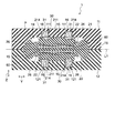
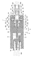
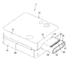
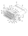
本開示の一実施形態のコネクタ1は、接続対象物の一例の検査装置100および検査対象200に接続可能に構成され(図3参照)、図1に示すように、コネクタハウジング10と、このコネクタハウジング10に揺動可能に支持されている第1端子接続部20とを備えている。コネクタハウジング10の内部には、図2に示すように、付勢部30が設けられている。
コネクタハウジング10は、図1に示すように、一例として、略矩形の箱状で、厚さ方向(すなわち、図1の上下方向)に積み重ねられた上ハウジング11と下ハウジング12とで構成されている。このコネクタハウジング10は、その長手方向(すなわち、第1方向X)に対向する側面の一方に開口面13を有し、この開口面13には、略楕円形状の開口部14が設けられている。
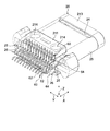
図3に示すように、コネクタハウジング10の内部には、基板40と、検査装置100に接続可能な第2端子接続部50とが設けられている。基板40は、その板面における第1方向Xの両端部に設けられた接続端子41(図6に示す)を介して、第1端子接続部20および第2端子接続部50に電気的に接続されている。第2端子接続部50は、基板40に対して第1方向Xにおける第1端子接続部20の反対側に配置されている。
第1端子接続部20は、図3に示すように、開口面13に交差(例えば、直交)する第1方向Xの一端部である第1端部201がコネクタハウジング10の内部に位置しかつ第1方向Xの他端部である第2端部202が検査対象200を接続可能にコネクタハウジング10の外部に露出している。なお、検査対象200は、例えば、USBコネクタあるいはHDMIコネクタを有する電子部品モジュールである。
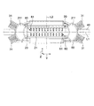
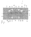
また、第1端子接続部20は、図4に示すように、開口部14内であって開口部14の縁部との間に隙間15が基準位置Pに配置され、開口面13上で図4の上下左右の任意の方向に対して揺動可能な状態で、コネクタハウジング10に支持されている。この実施形態では、隙間15は、基準位置Pにおいて、第1端子接続部20の第1方向X(すなわち、図2の紙面貫通方向)まわりの全周に亘って設けられている。
詳しくは、第1端子接続部20は、図3に示すように、板状のプローブピン60と、第1方向Xに延びて第1方向Xに交差(例えば、直交)する第2方向Y(図4に示す)に板面が対向するようにプローブピン60を収容可能な第1収容部22が設けられた接続ハウジング21とを有している。この実施形態では、第1端子接続部20は、図2に示すように、複数のプローブピン60を有し、接続ハウジング21には、第2方向Yに沿って間隔を空けて配置された複数対の第1収容部22が設けられ、各第1収容部22にプローブピン60がそれぞれ収容されている。これにより、各対の第1収容部22は、第1方向Xから見て、第1端子接続部20の第1方向Xおよび第2方向Yに交差(例えば、直交)する第3方向Zの中心線L1に対して対称に配置され、相互に電気的独立している。すなわち、各対の第1収容部22に収容されたプローブピン60は、後述する第1接触ばね部61によって検査対象200を第3方向Zから挟持可能であると共に、後述する第2接触ばね部62によって基板40を第3方向Zから挟持可能に構成されている。
図3に示すように、接続ハウジング21の第1端部201側の端部には、後述する付勢部30の付勢部材(すなわち、コイルばね31)を支持する支持部211が設けられ、接続ハウジング21の第2端部202側の端部には、第1方向Xに開口して第1方向Xから検査対象200を収容可能な凹部23と、確認用窓24とが設けられている。凹部23の内部には、各プローブピン60の後述する第1接触ばね部61が配置されている。すなわち、検査対象200は、第1方向Xに沿って第1端子接続部20に接続される。また、確認用窓24は、第1収容部22と接続ハウジング21の外部とに連通して、各プローブピン60の第1接触ばね部61を接続ハウジング21の外部から確認可能になっている。
また、図5に示すように、第1端子接続部20は、接続ハウジング21の外面を覆うと共に、コネクタハウジング10の内部に配置されるグランド端子26が設けられた導電性の外殻部25を有している。この実施形態では、外殻部25は、鉄等の金属で構成され、各プローブピン60とは電気的に独立した状態で接続ハウジング21の外面の第2端部202を除いた領域を覆っている。このように構成することで、第1端子接続部20に検査対象200を接続するときに、検査対象200が外殻部25に接触することがなくなり、第1端子接続部20への接続時における検査対象200の損傷を低減できる。また、グランド端子26は、外殻部25の第2方向Yの両端部のそれぞれに一対ずつ設けられている。
接続ハウジング21の外面には、図3に示すように、外殻部25を収容可能な凹部212が設けられている。この凹部212は、収容された外殻部25の外面が、接続ハウジング21の凹部212が設けられていない部分(例えば、接続ハウジング21の第2端部201側の端部213)の外面に対して、同一平面上に位置するように構成されている。
各対のグランド端子26は、図6に示すように、第3方向Zに対向するように配置され、第3方向Zに弾性変形した状態で基板40接続端子41に対して接触可能に構成されている。
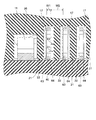
付勢部30は、図2に示すように、コネクタハウジング10の内部に配置されて、コネクタハウジング10に対して第1端子接続部20を基準位置Pに向かって付勢する。詳しくは、付勢部30は、複数の付勢部材(この実施形態では、4つのコイルばね31)で構成され、4つのコイルばね31が、第1方向Xに直交する仮想直線(例えば、第1端子接続部20の第3方向Zの中心線L1)に対して対称に配置されている。
各コイルばね31は、接続ハウジング21の支持部211に設けられた略円柱状の凹部214と、上ハウジング11および下ハウジング12の各々に設けられ相互に接続ハウジング21の凹部214にそれぞれ対向するように配置された略円柱状の凹部111、121とで構成されるコイルばね収容部16に収容されている。付勢部材としてコイルばね31を用いることで、第1端子接続部20を開口面13上の任意の方向に加えて、第1方向Xに揺動させることができる。
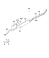
各プローブピン60は、図7に示すように、板状で、第1接触ばね部61および第2接触ばね部62と、第1接触ばね部61および第2接触ばね部62の間に第1方向Xに沿って直列的に配置された中間部63および緩衝ばね部64とを備えている。すなわち、第1接触ばね部61、中間部63、緩衝ばね部64および第2接触ばね部62は、第1方向Xに沿って配列されている。また、各プローブピン60は、例えば、電鋳法で形成され、第1接触ばね部61、中間部63、緩衝ばね部64および第2接触ばね部62が、一体に構成されている。
第1接触ばね部61および第2接触ばね部62の各々は、第2方向Yから見て、蛇行形状を有し、中間部63に対して第3方向Zに弾性変形可能に構成されている。また、第1接触ばね部61は、複数の帯状弾性片(この実施形態では、2つの帯状弾性片611、612)で構成されている。
中間部63は、略矩形状を有し、第1方向Xの両端部がそれぞれ第1接触ばね部61および緩衝ばね部64に接続されている。この中間部63の緩衝ばね部64側の端部には、接続ハウジング21の第1収容部22に収容されたときのプローブピン60の第1方向Xでかつ第2接触ばね部62に向かう方向の移動を規制する第1位置決め部631が設けられている。第1位置決め部631は、第3方向Zにおいて緩衝ばね部64から離れる方向に延びる平面で構成されている。
緩衝ばね部64は、中間部63から第3方向Zにおいて突出した略矩形の枠状を有し、第1方向Xの両端部がそれぞれ中間部63および第2接触ばね部62に接続され、中間部63に対して第2方向Y(すなわち、板厚方向)に弾性変形可能に構成されている。緩衝ばね部64の中間部63側の端部には、接続ハウジング21の第1収容部22に収容されたときのプローブピン60の第1方向Xでかつ第1接触ばね部61に向かう方向の移動を規制する第2位置決め部641が設けられている。第2位置決め部641は、第3方向Zにおいて緩衝ばね部64から離れる方向でかつ中間部63の第1位置決め部631とは反対方向に延びる平面で構成されている。
また、第2位置決め部641の第3方向Zにおける中間部63のから遠い方の端部には、第2位置決め部641から第1方向X沿いを第1接触ばね部62に向かって延びる突起部642が設けられている。この突起部642は、図3に示すように、第3方向Zにおいて、接続ハウジング21の支持部211に設けられ、コイルばね31と中間部63との間に配置された凹部215に収容されている。
図3に示すように、第2接触ばね部62および緩衝ばね部64の各々は、接続ハウジング21の外部でかつコネクタハウジング10の内部に位置している。緩衝ばね部64は、コネクタハウジング10の内部に設けられた第2収容部17に収容され、第2接触ばね部62は、コネクタハウジング10の内部に設けられた第3収容部18に収容されている。
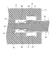
また、図8に示すように、第2方向Yにおける中間部63の板面と第1収容部22との間の最短距離D1が、第2方向Yにおける緩衝ばね部64の板面と第2収容部17との間の最短距離D2よりも小さくなっている。さらに、各プローブピン60の板厚W1が、隣接するプローブピン60の板面間の最短距離W2の1/2以下(好ましくは1/3以下)になるように構成されている。なお、図示していないが、第2方向Yにおける第2接触ばね部62の板面と第3収容部18との間の最短距離は、第2方向Yにおける中間部63の板面と第1収容部22との間の最短距離D1と略同一になっている。
前記コネクタ1では、開口部14が設けられた開口面13を有するコネクタハウジング10と、開口部14内であって開口部14の縁部との間に隙間15が設けられる基準位置Pに配置され、開口面13上で揺動可能な状態でコネクタハウジング10に支持されている第1端子接続部20と、第1端子接続部20を基準位置Pに向かって付勢する付勢部30とを備えている。このような構成により、検査対象200等の接続対象物が第1端子接続部20への接続方向(すなわち、第1方向X)に対して交差する方向から接続された場合であっても、付勢部30の付勢力に抗して第1端子接続部20が基準位置Pから一旦ずれたのち付勢部30の付勢力で第1端子接続部20を基準位置Pに戻すことができる。よって、第1端子接続部20を検査対象200等の接続対象物に対してセルフアライメントさせることができるので、検査対象200等の接続対象物を損傷させることなく接続可能なコネクタ1を実現できる。
また、第1端子接続部20が、その外面を覆うと共に、コネクタハウジング10の内部に配置されたグランド端子26が設けられた導電性の外殻部25を有している。この外殻部25により、コネクタを流れる高周波領域の信号の損失を低減できる。
また、コネクタハウジング10の内部に、第1端子接続部20に対して電気的に接続された基板40が設けられており、グランド端子26が、弾性変形した状態で基板40の接続端子41に接触可能に構成されている。このような構成により、グランド端子26の基板40の接続端子41に対する接圧を高めて、グランド端子26と接続端子41との間の接触信頼性を高めることができる。
また、付勢部30が、複数の付勢部材(例えば、コイルばね31)で構成されており、複数の付勢部材が、第1方向Xに直交する仮想直線L1に対して対称に配置されている。このような構成により、第1端子接続部20に対する付勢力のばらつきを低減して、より確実に第1端子接続部20を設計通りに揺動させることができる。その結果、第1端子接続部20を検査対象200等の接続対象物に対してより確実にセルフアライメントさせることができる。
また、第1端子接続部20が、板状のプローブピン60と、第1方向Xに延びて第2方向Yで板面が対向するようにプローブピン60を収容可能な第1収容部22が設けられた接続ハウジング21とを有し、プローブピン60は、第1接触ばね部61および第2接触ばね部62と、第1接触ばね部61および第2接触ばね部62の間に第1方向Xに沿って直列的に配置された中間部63および緩衝ばね部64とを備えている。第1接触ばね部61および第2接触ばね部62は、中間部63に対して第3方向Zに弾性変形可能に構成され、中間部63は、第1方向Xの両端部がそれぞれ第1接触ばね部61および緩衝ばね部64に接続され、緩衝ばね部64は、第1方向Xの両端部がそれぞれ中間部63および第2接触ばね部62に接続されていると共に、中間部63に対して第2方向Yに弾性変形可能に構成されている。第2接触ばね部62および緩衝ばね部64は、接続ハウジング21の外部でかつコネクタハウジング10の内部に位置し、コネクタハウジング10には、第1方向Xに延びて緩衝ばね部64を収容可能な第2収容部17が設けられている。そして、第2方向Yにおける中間部63の板面と第1収容部22との間の最短距離D1が、第2方向Yにおける緩衝ばね部64の板面と第2収容部17との間の最短距離D2よりも小さい。このような構成により、検査対象200等の接続対象物物が接触方向(すなわち、第1方向X)に交差する方向から第1端子接続部20に接続されて、プローブピン60に予定している接触方向に交差する方向(例えば、第2方向Y)の応力が加えられたとしても、緩衝ばね部64によりその応力を分散させて、プローブピン60の損傷を低減できる。すなわち、検査対象200等の接続対象物が接触方向に交差する方向から第1端子接続部20に接続された場合であっても、損傷し難いプローブピン60を実現できる。
また、接続ハウジング21が、第1収容部22と接続ハウジング21の外部とに連通すると共に、第1接触ばね部61を接続ハウジング21の外部から確認可能な確認用窓24を有している。この確認用窓24により、第1収容部22に収容されたプローブピン60の第1接触ばね部62の収容状態を容易に確認できる。
また、第1端子接続部20が、複数のプローブピン60と、第2方向Yに間隔を空けて配置され、各プローブピン60がそれぞれ収容された複数の第1収容部22とを有し、各プローブピン60の板厚W1が、隣接するプローブピン60の板面間の最短距離W2の1/2以下である。このような構成により、各プローブピン60の絶縁性を確実に確保することができる。
また、前記プローブピン60が、第1接触ばね部61および第2接触ばね部62の間に設けられ、第1収容部22に収容されたときの第1端子接続部20に対する第1方向Xの位置を決める位置決め部631、641をさらに備えている。この位置決め部631、641により、プローブピン60の第1収容部22からの脱落を低減できる。
また、位置決め部が、中間部63の第3方向Zの一方側に設けられ、第1方向Xの一方側(例えば、第2接触ばね部62に向かう方向)への移動を規制する第1位置決め部631と、緩衝ばね部64の第3方向Zの他方側に設けられ、第1方向Xの他方側(例えば、第2接触ばね部61に向かう方向)への移動を規制する第2位置決め部641とを有している。このような構成により、プローブピン60の第1収容部22からの脱落をより低減できる。
なお、前記コネクタ1では、コネクタハウジング10が、第3方向Zに積層された上ハウジング11および下ハウジング12で構成されているが、これに限らない。例えば、図9に示すように、第2方向Yに積層された左ハウジング71および右ハウジング72で構成してもよい。この場合、図10に示すように、付勢部30の4つのコイルばね31は、第1方向X(すなわち、図10の紙面貫通方向)から見て、第1端子接続部20の第2方向Yの中心線L2に対して対称に配置することができる。
また、第1収容部22に収容されたプローブピン60の中間部63の板面と第1収容部22との間の最短距離D1が、このプローブピン60の緩衝ばね部64の板面と第2収容部17との間の最短距離D2よりも小さくなるように構成されているが、これに限らず、例えば、最短距離D1と最短距離D2とが同じになるように構成してもよい。
外殻部25は、接続ハウジング21の一部を覆うように構成されている場合に限らず、例えば、図9に示すように、接続ハウジング21の全体を覆うように構成してもよいし、高周波領域の信号の損失をあまり考慮する必要がない場合には、省略することもできる。
グランド端子26は、弾性変形した状態で基板40の接続端子41に接触するように構成されている場合に限らず、弾性変形していない状態で基板40の接続端子41に接触するように構成してもよい。この場合、例えば、グランド端子26は、基板40の接続端子41に半田付け等により接続して、接触信頼性を高めるようにしてもよい。
付勢部30は、4つのコイルばね31で構成されている場合に限らず、例えば、1~3のコイルばね31で構成してもよいし、5以上のコイルばね31で構成してもよい。また、付勢部30は、複数のコイルばね31を第3方向Zの上下に配置する場合に限らず、複数のコイルばね31を第3方向Zの上下に加えて、第2方向Yの左右の一方または両方に配置してもよい。
付勢部材は、コイルばね31に限らず、例えば、図12に示すように、板ばね32で構成してもよい。図12では、第3方向Zの上下に板ばね32をそれぞれ2つずつ配置し(図12には、3つの板ばね32のみ示す)、第2方向Yの左右の両方に板ばね32をそれぞれ2つずつ配置している。
端子接続部は、コネクタ1の設計等に応じて、その構成を適宜変更できる。
例えば、第1端子接続部20のプローブピンは、前記プローブピン60に限らず、他の構成のプローブピンを用いることもできる。例えば、第1端子接続部20のプローブピンとして、電鋳法以外の方法で形成されたプローブピンを用いることもできるし、位置決め部631、641を設けていないプローブピンを用いることもできる。
また、接続ハウジング21は、第2方向Yに沿って間隔を空けて配置された複数対の第1収容部22を有する場合に限らず、例えば、図13に示すように、第3方向Zの中心線L1に対する一方側(図13では、第3方向Zの中心線L1の上ハウジング11側)のみに、複数の第1収容部22を設けてもよい。この場合、外殻部25のグランド端子26も、第3方向Zの中心線L1の一方側のみに設ければよい。
また、第1端子接続部20の複数のプローブピン60は、図5に示すように、第1接触ばね部61および第2接触ばね部62の先端部が、第2方向Yに沿って一直線に並ぶように配置されている(図5では、第2接触ばね部62のみ示す)が、これに限らない。例えば、第1接触ばね部61および第2接触ばね部62の先端部が交互に第1方向Xにずれた千鳥状に、複数のプローブピン60を配置してもよい。
また、図14に示すように、確認用窓24を省略してもよい。
また、各プローブピン60の板厚W1が、隣接するプローブピン60の板面間の最短距離W2の1/2以下(好ましくは1/3以下)になるように構成されている場合に限らず、各プローブピン60の板厚W1が、隣接するプローブピン60の板面間の最短距離W2の1/2よりも大きくなるように構成することもできる。
以上、図面を参照して本開示における種々の実施形態を詳細に説明したが、最後に、本開示の種々の態様について説明する。なお、以下の説明では、一例として、参照符号も添えて記載する。
本開示の第1態様のコネクタ1は、
接続対象物100、200に接続可能なコネクタ1であって、
開口部14が設けられた開口面13を有するコネクタハウジング10と、
前記開口面13に交差する第1方向Xの一端部が前記コネクタハウジング10の内部に位置しかつ前記第1方向Xの他端部が前記接続対象200を接続可能に前記コネクタハウジング10の外部に露出していると共に、前記開口部14内であって前記開口部14の縁部との間に隙間15が設けられる基準位置Pに配置され、前記開口面13上で揺動可能な状態で前記コネクタハウジング10に支持されている端子接続部20と、
前記コネクタハウジング10の内部に配置されて、前記コネクタハウジング10に対して前記端子接続部20を前記基準位置Pに向かって付勢する付勢部30と
を備える。
接続対象物100、200に接続可能なコネクタ1であって、
開口部14が設けられた開口面13を有するコネクタハウジング10と、
前記開口面13に交差する第1方向Xの一端部が前記コネクタハウジング10の内部に位置しかつ前記第1方向Xの他端部が前記接続対象200を接続可能に前記コネクタハウジング10の外部に露出していると共に、前記開口部14内であって前記開口部14の縁部との間に隙間15が設けられる基準位置Pに配置され、前記開口面13上で揺動可能な状態で前記コネクタハウジング10に支持されている端子接続部20と、
前記コネクタハウジング10の内部に配置されて、前記コネクタハウジング10に対して前記端子接続部20を前記基準位置Pに向かって付勢する付勢部30と
を備える。
第1態様のコネクタ1によれば、検査対象200等の接続対象物物が端子接続部20への接続方向(すなわち、第1方向X)に対して交差する方向から接続された場合であっても、付勢部30の付勢力に抗して端子接続部20が基準位置Pから一旦ずれたのち付勢部30の付勢力で第1端子接続部20を基準位置Pに戻すことができる。よって、端子接続部20を検査対象200等の接続対象物物に対してセルフアライメントさせることができるので、検査対象200等の接続対象物を損傷させることなく接続可能なコネクタ1を実現できる。
本開示の第2態様のコネクタ1は、
前記端子接続部20が、その外面を覆うと共に、前記コネクタハウジング10の内部に配置されたグランド端子26が設けられた導電性の外殻部25を有している。
前記端子接続部20が、その外面を覆うと共に、前記コネクタハウジング10の内部に配置されたグランド端子26が設けられた導電性の外殻部25を有している。
第2態様のコネクタ1によれば、外殻部25により、コネクタを流れる高周波領域の信号の損失を低減できる。
本開示の第3態様のコネクタ1は、
前記コネクタハウジング10の内部に、前記端子接続部20に対して電気的に接続された基板40が設けられており、
前記グランド端子26が、弾性変形した状態で前記基板の接続端子41に接触可能に構成されている。
前記コネクタハウジング10の内部に、前記端子接続部20に対して電気的に接続された基板40が設けられており、
前記グランド端子26が、弾性変形した状態で前記基板の接続端子41に接触可能に構成されている。
第3態様のコネクタ1によれば、グランド端子26の基板40の接続端子41に対する接圧を高めて、グランド端子26と接続端子41との間の接触信頼性を高めることができる。
本開示の第4態様のコネクタ1は、
前記付勢部30が、複数の付勢部材31、32で構成されており、
前記複数の付勢部材31、32が、前記第1方向Xに直交する仮想直線L1に対して対称に配置されている。
前記付勢部30が、複数の付勢部材31、32で構成されており、
前記複数の付勢部材31、32が、前記第1方向Xに直交する仮想直線L1に対して対称に配置されている。
第4態様のコネクタ1によれば、端子接続部20に対する付勢力のばらつきを低減して、より確実に端子接続部20を設計通りに揺動させることができる。その結果、端子接続部20を検査対象200等の接続対象物に対してより確実にセルフアライメントさせることができる。
本開示の第5態様のコネクタ1は、
前記端子接続部20が、
板状のプローブピン60と、
前記第1方向Xに延びて前記第1方向Xに交差する第2方向Yで板面が対向するように前記プローブピン60を収容可能な第1収容部22が設けられた接続ハウジング21と
を有し、
前記プローブピン60は、
第1接触ばね部61および第2接触ばね部62と、
前記第1接触ばね部61および前記第2接触ばね部62の間に前記第1方向Xに沿って直列的に配置された中間部63および緩衝ばね部64と
を備え、
前記第1接触ばね部61および前記第2接触ばね部62は、前記中間部63に対して前記第1方向Xおよび前記第2方向Yに交差する第3方向Zに弾性変形可能に構成され、
前記中間部63は、前記第1方向Xの両端部がそれぞれ前記第1接触ばね部61および前記緩衝ばね部64に接続され、
前記緩衝ばね部64は、前記第1方向Xの両端部がそれぞれ前記中間部63および前記第2接触ばね部62に接続されていると共に、前記中間部63に対して前記第2方向Yに弾性変形可能に構成されており、
前記第2接触ばね部62および前記緩衝ばね部64は、前記接続ハウジング21の外部でかつ前記コネクタハウジング10の内部に位置し、
前記コネクタハウジング10には、前記第1方向Xに延びて前記緩衝ばね部64を収容可能な第2収容部17が設けられており、
前記第2方向Yにおける前記中間部63の板面と前記第1収容部22との間の最短距離D1が、前記第2方向Yにおける前記緩衝ばね部64の板面と前記第2収容部17との間の最短距離D2よりも小さい。
前記端子接続部20が、
板状のプローブピン60と、
前記第1方向Xに延びて前記第1方向Xに交差する第2方向Yで板面が対向するように前記プローブピン60を収容可能な第1収容部22が設けられた接続ハウジング21と
を有し、
前記プローブピン60は、
第1接触ばね部61および第2接触ばね部62と、
前記第1接触ばね部61および前記第2接触ばね部62の間に前記第1方向Xに沿って直列的に配置された中間部63および緩衝ばね部64と
を備え、
前記第1接触ばね部61および前記第2接触ばね部62は、前記中間部63に対して前記第1方向Xおよび前記第2方向Yに交差する第3方向Zに弾性変形可能に構成され、
前記中間部63は、前記第1方向Xの両端部がそれぞれ前記第1接触ばね部61および前記緩衝ばね部64に接続され、
前記緩衝ばね部64は、前記第1方向Xの両端部がそれぞれ前記中間部63および前記第2接触ばね部62に接続されていると共に、前記中間部63に対して前記第2方向Yに弾性変形可能に構成されており、
前記第2接触ばね部62および前記緩衝ばね部64は、前記接続ハウジング21の外部でかつ前記コネクタハウジング10の内部に位置し、
前記コネクタハウジング10には、前記第1方向Xに延びて前記緩衝ばね部64を収容可能な第2収容部17が設けられており、
前記第2方向Yにおける前記中間部63の板面と前記第1収容部22との間の最短距離D1が、前記第2方向Yにおける前記緩衝ばね部64の板面と前記第2収容部17との間の最短距離D2よりも小さい。
第5態様のコネクタ1によれば、検査対象200等の接続対象物物が接触方向(すなわち、第1方向X)に交差する方向から端子接続部20に接続されて、プローブピン60に接触方向に交差する方向(例えば、第2方向Y)の応力が加わったとしても、緩衝ばね部64によりその応力を分散させて、プローブピン60の損傷を低減できる。すなわち、検査対象200等の接続対象物が接触方向に交差する方向から端子接続部20に接続された場合であっても、損傷し難いプローブピン60を実現できる。
本開示の第6態様のコネクタ1は、
前記接続ハウジング21が、前記第1収容部22と前記接続ハウジング21の外部とに連通すると共に、前記第1接触ばね部61を前記接続ハウジング21の外部から確認可能な確認用窓24を有している。
前記接続ハウジング21が、前記第1収容部22と前記接続ハウジング21の外部とに連通すると共に、前記第1接触ばね部61を前記接続ハウジング21の外部から確認可能な確認用窓24を有している。
第6態様のコネクタ1によれば、確認用窓24により、第1収容部22に収容されたプローブピン60の接触ばね部62の収容状態を容易に確認できる。
本開示の第7態様のコネクタ1は、
前記端子接続部20が、
複数の前記プローブピン60と、
前記第2方向Yに間隔を空けて配置され、前記プローブピン60がそれぞれ収容された複数の前記第1収容部22と
を有し、
前記プローブピン60の板厚W1が、隣接する前記プローブピン60の板面間の最短距離W1の1/2以下である。
前記端子接続部20が、
複数の前記プローブピン60と、
前記第2方向Yに間隔を空けて配置され、前記プローブピン60がそれぞれ収容された複数の前記第1収容部22と
を有し、
前記プローブピン60の板厚W1が、隣接する前記プローブピン60の板面間の最短距離W1の1/2以下である。
第7態様のコネクタ1によれば、各プローブピン60の絶縁性を確実に確保することができる。
なお、前記様々な実施形態または変形例のうちの任意の実施形態または変形例を適宜組み合わせることにより、それぞれの有する効果を奏するようにすることができる。また、実施形態同士の組み合わせまたは実施例同士の組み合わせまたは実施形態と実施例との組み合わせが可能であると共に、異なる実施形態または実施例の中の特徴同士の組み合わせも可能である。
本開示のコネクタは、例えば、USBデバイスあるいはHDMIデバイスの検査に用いることができる。
1 コネクタ
10 コネクタハウジング
11 上ハウジング
111 凹部
12 下ハウジング
121 凹部
13 開口面
14 開口部
15 隙間
16 コイルばね収容部
17 第2収容部
18 第3収容部
20 第1端子接続部
201 第1端部
202 第2端部
21 接続ハウジング
211 支持部
212 凹部
213 端部
214、215 凹部
22 第1収容部
23 凹部
24 確認用窓
25 外殻部
26 グランド端子
30 付勢部
31 コイルばね
32 板ばね
40 基板
50 第2端子接続部
60 プローブピン
61 第1接触ばね部
611、612 帯状弾性片
62 第2接触ばね部
63 中間部
631 第1位置決め部
64 緩衝ばね部
641 第2位置決め部
642 突起部
71 左ハウジング
72 右ハウジング
100 検査装置
200 検査対象
L1、L2 中心線
P 基準位置
X 第1方向
Y 第2方向
Z 第3方向
D1、D2 最短距離
W1 板厚
W2 最短距離
10 コネクタハウジング
11 上ハウジング
111 凹部
12 下ハウジング
121 凹部
13 開口面
14 開口部
15 隙間
16 コイルばね収容部
17 第2収容部
18 第3収容部
20 第1端子接続部
201 第1端部
202 第2端部
21 接続ハウジング
211 支持部
212 凹部
213 端部
214、215 凹部
22 第1収容部
23 凹部
24 確認用窓
25 外殻部
26 グランド端子
30 付勢部
31 コイルばね
32 板ばね
40 基板
50 第2端子接続部
60 プローブピン
61 第1接触ばね部
611、612 帯状弾性片
62 第2接触ばね部
63 中間部
631 第1位置決め部
64 緩衝ばね部
641 第2位置決め部
642 突起部
71 左ハウジング
72 右ハウジング
100 検査装置
200 検査対象
L1、L2 中心線
P 基準位置
X 第1方向
Y 第2方向
Z 第3方向
D1、D2 最短距離
W1 板厚
W2 最短距離
Claims (7)
- 接続対象物に接続可能なコネクタであって、
開口部が設けられた開口面を有するコネクタハウジングと、
前記開口面に交差する第1方向の一端部が前記コネクタハウジングの内部に位置しかつ前記第1方向の他端部が前記接続対象物を接続可能に前記コネクタハウジングの外部に露出していると共に、前記開口部内で前記開口部の縁部との間に隙間が設けられる基準位置に配置され、前記開口面上で揺動可能な状態で前記コネクタハウジングに支持されている端子接続部と、
前記コネクタハウジングの内部に配置されて、前記コネクタハウジングに対して前記端子接続部を前記基準位置に向かって付勢する付勢部と
を備える、コネクタ。 - 前記端子接続部が、その外面を覆うと共に、前記コネクタハウジングの内部に配置されたグランド端子が設けられた導電性の外殻部を有している、請求項1のコネクタ。
- 前記コネクタハウジングの内部に、前記端子接続部に対して電気的に接続された基板が設けられており、
前記グランド端子が、弾性変形した状態で前記基板の接続端子に接触可能に構成されている、請求項2のコネクタ。 - 前記付勢部が、複数の付勢部材で構成されており、
前記複数の付勢部材が、前記第1方向に直交する仮想直線に対して対称に配置されている、請求項1から3のいずれか1つのコネクタ。 - 前記端子接続部が、
板状のプローブピンと、
前記第1方向に延びて前記第1方向に交差する第2方向で板面が対向するように前記プローブピンを収容可能な第1収容部が設けられた接続ハウジングと
を有し、
前記プローブピンは、
第1接触ばね部および第2接触ばね部と、
前記第1接触ばね部および前記第2接触ばね部の間に前記第1方向に沿って直列的に配置された中間部および緩衝ばね部と
を備え、
前記第1接触ばね部および前記第2接触ばね部は、前記中間部に対して前記第1方向および前記第2方向に交差する第3方向に弾性変形可能に構成され、
前記中間部は、前記第1方向の両端部がそれぞれ前記第1接触ばね部および前記緩衝ばね部に接続され、
前記緩衝ばね部は、前記第1方向の両端部がそれぞれ前記中間部および前記第2接触ばね部に接続されていると共に、前記中間部に対して前記第2方向に弾性変形可能に構成されており、
前記第2接触ばね部および前記緩衝ばね部は、前記接続ハウジングの外部でかつ前記コネクタハウジングの内部に位置し、
前記コネクタハウジングには、前記第1方向に延びて前記緩衝ばね部を収容可能な第2収容部が設けられており、
前記第2方向における前記中間部の板面と前記第1収容部との間の最短距離が、前記第2方向における前記緩衝ばね部の板面と前記第2収容部との間の最短距離よりも小さい、請求項1から4のいずれか1つのコネクタ。 - 前記接続ハウジングが、前記第1収容部と前記接続ハウジングの外部とに連通すると共に、前記第1接触ばね部を前記接続ハウジングの外部から確認可能な確認用窓を有している、請求項5のコネクタ。
- 前記端子接続部が、
複数の前記プローブピンと、
前記第2方向に間隔を空けて配置され、前記プローブピンがそれぞれ収容された複数の前記第1収容部と
を有し、
前記プローブピンの板厚が、隣接する前記プローブピンの板面間の最短距離の1/2以下である、請求項5または6のコネクタ。
Priority Applications (2)
| Application Number | Priority Date | Filing Date | Title |
|---|---|---|---|
| CN201980027033.6A CN112005449B (zh) | 2018-05-22 | 2019-05-15 | 连接器 |
| KR1020207029955A KR102454259B1 (ko) | 2018-05-22 | 2019-05-15 | 커넥터 |
Applications Claiming Priority (2)
| Application Number | Priority Date | Filing Date | Title |
|---|---|---|---|
| JP2018098188A JP7067265B2 (ja) | 2018-05-22 | 2018-05-22 | コネクタ |
| JP2018-098188 | 2018-05-22 |
Publications (1)
| Publication Number | Publication Date |
|---|---|
| WO2019225432A1 true WO2019225432A1 (ja) | 2019-11-28 |
Family
ID=68616098
Family Applications (1)
| Application Number | Title | Priority Date | Filing Date |
|---|---|---|---|
| PCT/JP2019/019287 Ceased WO2019225432A1 (ja) | 2018-05-22 | 2019-05-15 | コネクタ |
Country Status (5)
| Country | Link |
|---|---|
| JP (1) | JP7067265B2 (ja) |
| KR (1) | KR102454259B1 (ja) |
| CN (1) | CN112005449B (ja) |
| TW (1) | TWI708440B (ja) |
| WO (1) | WO2019225432A1 (ja) |
Families Citing this family (2)
| Publication number | Priority date | Publication date | Assignee | Title |
|---|---|---|---|---|
| KR102342154B1 (ko) * | 2020-02-25 | 2021-12-22 | 주식회사 엠투아이코퍼레이션 | 커넥터 지지장치 |
| US20250087950A1 (en) * | 2021-07-19 | 2025-03-13 | Molex, Llc | Busbar assembly |
Citations (4)
| Publication number | Priority date | Publication date | Assignee | Title |
|---|---|---|---|---|
| JP3175979U (ja) * | 2011-06-30 | 2012-06-07 | 周賢 蔡 | シェルを備えた両面オスコネクタ |
| JP2013030452A (ja) * | 2011-06-20 | 2013-02-07 | Japan Aviation Electronics Industry Ltd | Usbコネクタ |
| US20140134883A1 (en) * | 2012-11-15 | 2014-05-15 | Iriso Electronics Co., Ltd. | Electric Connection Terminal and Connector Including the Same |
| WO2016160034A1 (en) * | 2015-04-03 | 2016-10-06 | Hewlett Packard Enterprise Development Lp | Connector mounts |
Family Cites Families (11)
| Publication number | Priority date | Publication date | Assignee | Title |
|---|---|---|---|---|
| JP2597035Y2 (ja) * | 1993-06-21 | 1999-06-28 | 住友電装株式会社 | コネクタ導通検査装置 |
| JP4451386B2 (ja) * | 2005-12-20 | 2010-04-14 | ヒロセ電機株式会社 | 電気コネクタ |
| US8690608B2 (en) * | 2011-06-20 | 2014-04-08 | Japan Aviation Electronics Industry Limited | Special USB plug having different structure from standard USB plug and USB receptacle matable with the special USB plug |
| JP4938148B1 (ja) * | 2011-06-27 | 2012-05-23 | 日本航空電子工業株式会社 | コンタクトおよびコネクタ |
| JP5840649B2 (ja) * | 2013-05-29 | 2016-01-06 | ヒロセ電機株式会社 | 電気コネクタ、該電気コネクタと相手コネクタとを有する電気コネクタ組立体 |
| JP5946804B2 (ja) * | 2013-08-09 | 2016-07-06 | ヒロセ電機株式会社 | コネクタ |
| JP6273119B2 (ja) * | 2013-10-08 | 2018-01-31 | 株式会社東芝 | 電気機器の接続装置 |
| DE102013111905B9 (de) * | 2013-10-29 | 2015-10-29 | Telegärtner Karl Gärtner GmbH | Verbindungseinrichtung zum elektrischen Verbinden zweier Leiterplatten |
| JP5568677B1 (ja) * | 2013-11-13 | 2014-08-06 | イリソ電子工業株式会社 | 電気コネクタ |
| JP6192567B2 (ja) | 2014-02-21 | 2017-09-06 | ケル株式会社 | フローティング型コネクタ |
| JP6507135B2 (ja) * | 2016-03-15 | 2019-04-24 | 宏致電子股▲ふん▼有限公司Aces Electronics Co.,Ltd. | プラグユニット及びレセプタクルユニット |
-
2018
- 2018-05-22 JP JP2018098188A patent/JP7067265B2/ja active Active
-
2019
- 2019-05-15 KR KR1020207029955A patent/KR102454259B1/ko active Active
- 2019-05-15 CN CN201980027033.6A patent/CN112005449B/zh active Active
- 2019-05-15 WO PCT/JP2019/019287 patent/WO2019225432A1/ja not_active Ceased
- 2019-05-20 TW TW108117304A patent/TWI708440B/zh active
Patent Citations (4)
| Publication number | Priority date | Publication date | Assignee | Title |
|---|---|---|---|---|
| JP2013030452A (ja) * | 2011-06-20 | 2013-02-07 | Japan Aviation Electronics Industry Ltd | Usbコネクタ |
| JP3175979U (ja) * | 2011-06-30 | 2012-06-07 | 周賢 蔡 | シェルを備えた両面オスコネクタ |
| US20140134883A1 (en) * | 2012-11-15 | 2014-05-15 | Iriso Electronics Co., Ltd. | Electric Connection Terminal and Connector Including the Same |
| WO2016160034A1 (en) * | 2015-04-03 | 2016-10-06 | Hewlett Packard Enterprise Development Lp | Connector mounts |
Also Published As
| Publication number | Publication date |
|---|---|
| TW202005191A (zh) | 2020-01-16 |
| TWI708440B (zh) | 2020-10-21 |
| CN112005449B (zh) | 2022-08-12 |
| CN112005449A (zh) | 2020-11-27 |
| JP7067265B2 (ja) | 2022-05-16 |
| JP2019204645A (ja) | 2019-11-28 |
| KR102454259B1 (ko) | 2022-10-14 |
| KR20200128576A (ko) | 2020-11-13 |
Similar Documents
| Publication | Publication Date | Title |
|---|---|---|
| KR102103370B1 (ko) | 프로브 핀, 검사 지그, 검사 유닛 및 검사 장치 | |
| JP7314633B2 (ja) | プローブピン、検査治具および検査ユニット | |
| JP2019138709A (ja) | プローブピン、検査治具、検査ユニットおよび検査装置 | |
| TWI709749B (zh) | 檢查具、檢查單元以及檢查裝置 | |
| WO2017217043A1 (ja) | ソケット | |
| CN112534276B (zh) | 探针单元 | |
| JP2020201121A (ja) | プローブピン、検査治具および検査ユニット | |
| KR102430924B1 (ko) | 커넥터 및 커넥터 조립체 | |
| KR101851519B1 (ko) | 소켓, 검사 지그, 검사 유닛 및 검사 장치 | |
| JP7067265B2 (ja) | コネクタ | |
| JP7226441B2 (ja) | プローブピン | |
| JP7371374B2 (ja) | プローブユニット | |
| JP2015185421A (ja) | コネクタ及びコネクタの中継接続構造 | |
| JP2019158368A (ja) | 検査ユニットおよび検査装置 | |
| JP2024064484A (ja) | 同型コネクタと接続可能なコネクタ装置 |
Legal Events
| Date | Code | Title | Description |
|---|---|---|---|
| 121 | Ep: the epo has been informed by wipo that ep was designated in this application |
Ref document number: 19807046 Country of ref document: EP Kind code of ref document: A1 |
|
| ENP | Entry into the national phase |
Ref document number: 20207029955 Country of ref document: KR Kind code of ref document: A |
|
| NENP | Non-entry into the national phase |
Ref country code: DE |
|
| 122 | Ep: pct application non-entry in european phase |
Ref document number: 19807046 Country of ref document: EP Kind code of ref document: A1 |