WO2019215840A1 - インクジェットヘッド、及び画像形成装置 - Google Patents
インクジェットヘッド、及び画像形成装置 Download PDFInfo
- Publication number
- WO2019215840A1 WO2019215840A1 PCT/JP2018/017922 JP2018017922W WO2019215840A1 WO 2019215840 A1 WO2019215840 A1 WO 2019215840A1 JP 2018017922 W JP2018017922 W JP 2018017922W WO 2019215840 A1 WO2019215840 A1 WO 2019215840A1
- Authority
- WO
- WIPO (PCT)
- Prior art keywords
- data
- inkjet head
- image data
- ink
- fixed value
- Prior art date
- Legal status (The legal status is an assumption and is not a legal conclusion. Google has not performed a legal analysis and makes no representation as to the accuracy of the status listed.)
- Ceased
Links
Images













Classifications
-
- B—PERFORMING OPERATIONS; TRANSPORTING
- B41—PRINTING; LINING MACHINES; TYPEWRITERS; STAMPS
- B41J—TYPEWRITERS; SELECTIVE PRINTING MECHANISMS, i.e. MECHANISMS PRINTING OTHERWISE THAN FROM A FORME; CORRECTION OF TYPOGRAPHICAL ERRORS
- B41J2/00—Typewriters or selective printing mechanisms characterised by the printing or marking process for which they are designed
- B41J2/005—Typewriters or selective printing mechanisms characterised by the printing or marking process for which they are designed characterised by bringing liquid or particles selectively into contact with a printing material
- B41J2/01—Ink jet
- B41J2/015—Ink jet characterised by the jet generation process
- B41J2/04—Ink jet characterised by the jet generation process generating single droplets or particles on demand
- B41J2/045—Ink jet characterised by the jet generation process generating single droplets or particles on demand by pressure, e.g. electromechanical transducers
-
- B—PERFORMING OPERATIONS; TRANSPORTING
- B41—PRINTING; LINING MACHINES; TYPEWRITERS; STAMPS
- B41J—TYPEWRITERS; SELECTIVE PRINTING MECHANISMS, i.e. MECHANISMS PRINTING OTHERWISE THAN FROM A FORME; CORRECTION OF TYPOGRAPHICAL ERRORS
- B41J2/00—Typewriters or selective printing mechanisms characterised by the printing or marking process for which they are designed
- B41J2/005—Typewriters or selective printing mechanisms characterised by the printing or marking process for which they are designed characterised by bringing liquid or particles selectively into contact with a printing material
- B41J2/01—Ink jet
- B41J2/135—Nozzles
- B41J2/14—Structure thereof only for on-demand ink jet heads
Definitions
- the present disclosure relates to an inkjet head and an image forming apparatus.
- an inkjet head that has a plurality of ink channels that are partitioned by wall portions that constitute a piezoelectric element, and that drives the plurality of ink channels separately by supplying voltage to the piezoelectric elements of the plurality of ink channels.
- Patent Document 1 Japanese Patent Document 1
- an ink jet head using a shear mode type piezoelectric element (also referred to as a shear mode ink jet head) is known.
- the shear mode type ink jet head has a pressure chamber (hereinafter referred to as “ink channel”) for discharging ink and an air chamber (not referred to as “ink channel”) for discharging ink across a wall portion (hereinafter referred to as “driving wall”) as a piezoelectric member.
- ink channel a pressure chamber
- an air chamber not referred to as “ink channel”
- driving wall a wall portion
- electrodes on one side for applying a voltage to the drive wall are disposed in the ink channel on both side surfaces of the drive wall, and electrodes on the other side for applying a voltage to the drive wall in the air channel. Is provided, thereby forming a piezoelectric element.
- the ink jet head applies a voltage to the pair of electrodes disposed on both side surfaces of the drive wall, thereby shearing the drive wall and ejecting ink in the ink channel from the nozzle (FIG. 3A). , Described later with reference to FIGS. 3B and 3C).
- this type of ink-jet head has individually controlled the voltage supply to the piezoelectric elements of each of the plurality of ink channels by means of a driver IC, thereby driving each of the plurality of ink channels independently. ing.
- the driver IC drives and controls one ink channel
- the driver IC individually controls one electrode of the piezoelectric element (for example, an electrode disposed in the ink channel) at a timing of expanding the ink channel.
- the present disclosure has been made in view of the above-described problems, and an object thereof is to provide an inkjet head and an image forming apparatus that are suitable for realizing high-quality printing images and high-speed printing.
- An ink-jet head having a plurality of ink channels divided by wall portions constituting a piezoelectric element, and driving the plurality of ink channels separately by supplying voltage to the piezoelectric elements of the plurality of ink channels, respectively;
- Image data transferred from the main body of the image forming apparatus is stored in a shift register, and a driving voltage is individually applied to one electrode of the piezoelectric element of each of the plurality of ink channels based on the image data.
- a second drive circuit that supplies a common voltage common to the plurality of ink channels to the other electrode of the piezoelectric element of each of the plurality of ink channels;
- the first drive circuit only has the pixel data obtained by thinning out the fixed value data of the image data in which pixel data and fixed value data are alternately arranged for each bit transferred from the main body.
- a fixed value data removal circuit that relays between the main body and the shift register so as to be stored in order in the shift register;
- the first drive circuit and the second drive circuit are inkjet heads that operate in synchronization according to a predetermined timing command signal.
- An image forming apparatus including the inkjet head.
- the inkjet head according to the present disclosure is suitable for realizing high image quality of printing images and high-speed printing.
- FIG. 1 is a block diagram illustrating an example of a configuration of an image forming apparatus according to a first embodiment.
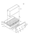
- 1 is an exploded perspective view illustrating an example of a configuration of a head main body according to a first embodiment.
- Side surface sectional drawing which shows an example of a structure of the head main body which concerns on 1st Embodiment.
- Side surface sectional drawing which shows an example of a structure of the head main body which concerns on 1st Embodiment.
- Side surface sectional drawing which shows an example of a structure of the head main body which concerns on 1st Embodiment.
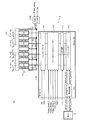
- the figure which shows an example of a structure of the drive part which concerns on 1st Embodiment.
- the figure explaining the function of the fixed value data removal circuit which concerns on 1st Embodiment The figure explaining the function of the fixed value data removal circuit which concerns on 1st Embodiment
- the figure explaining the function of the fixed value data removal circuit which concerns on 1st Embodiment The figure explaining the function of the fixed value data removal circuit which concerns on 1st Embodiment
- the figure explaining the function of the fixed value data removal circuit which concerns on 1st Embodiment The figure which shows an example of a structure of the fixed value data removal circuit which concerns on 1st Embodiment. 4 is a timing chart showing an example of a sequence of a write operation and a read operation in the fixed value data removal circuit according to the first embodiment.
- the figure which shows an example of the conversion table of the pixel data and the drive waveform pattern data which the gray scale controller which concerns on 1st Embodiment refers The figure which shows three types of drive waveforms in the drive waveform pattern data of FIG.
- the figure which shows an example of the output waveform which a buffer amplifier outputs to an individual electrode based on the drive signal of the gray scale controller which concerns on 1st Embodiment 1 is a diagram showing an example of the configuration of a buffer amplifier and a COM driver according to a first embodiment In the ink jet head according to the prior art, a diagram showing a difference in operation between driving only one piezoelectric element (left figure) and driving two adjacent piezoelectric elements simultaneously (right figure).
- produced in the inkjet head which concerns on a prior art The figure which shows an example of a structure of the drive part of the inkjet head which concerns on 2nd Embodiment.
- FIG. 1 is a block diagram illustrating an example of the configuration of the image forming apparatus 1.
- the image forming apparatus 1 includes a main body 2 and inkjet heads 100Y, 100M, 100C, and 100K corresponding to colors of yellow, magenta, cyan, and black.
- the inkjet heads 100Y, 100M, 100C, and 100K are controlled by the main body 2 via the signal lines 19, respectively.
- the inkjet heads 100Y, 100M, 100C, and 100K include driving units 110Y, 110M, 110C, and 110K, and head bodies 120Y, 120M, 120C, and 120K, respectively.
- driving units 110Y, 110M, 110C, and 110K head bodies 120Y, 120M, 120C, and 120K, respectively.
- head bodies 120Y, 120M, 120C, and 120K respectively.
- the respective configurations of the inkjet heads 100Y, 100M, 100C, and 100K are simply referred to as “inkjet head 100”, “driving unit 110”, and “head main body 120”, assuming that they have the same configuration. explain.
- the main body 2 includes a CPU (Central Processing Unit) 11, a RAM (Random Access Memory) 12 electrically connected to the CPU 11, a ROM (Read Only Memory) 13, an interface 14, a page memory 15, a line memory 16, and a control circuit 17. And a drive signal generation circuit 18.
- a CPU Central Processing Unit
- RAM Random Access Memory
- ROM Read Only Memory
- the CPU 11 reads a program stored in the ROM 13 into the RAM 12 and controls the operation of each unit of the image forming apparatus 1 according to the program.
- the interface 14 is means for transmitting and receiving data to and from the external device 4 such as a personal computer, and is configured by any one of various serial interfaces, various parallel interfaces, or a combination thereof.
- the page memory 15 stores image data to be printed transmitted from the external device 4.
- the “image data” stored in the page memory 15 is data of the entire image to be printed, and includes, for example, address data indicating the position in the two-dimensional plane of the image to be printed and pixel data at the position.
- Consists of. “Pixel data” is gradation data for each pixel area in “image data”, and corresponds to the ink ejection amount ejected by each nozzle of the head main body 120 in one pixel area. In other words, the ejection operation in one pixel region of one nozzle is controlled based on one “pixel data”.
- the “pixel data” according to the present embodiment represents the gradation of one pixel area with 3 bits.
- the line memory 16 is a memory that temporarily stores pixel data to be ejected by each nozzle of the head main body 120 among the image data stored in the page memory 15 when an image is printed on a recording medium.
- the line memory 16 sequentially transfers the stored image data to the drive unit 110. Note that data transfer from the page memory 15 to the line memory 16 is executed under the control of the CPU 11.
- the “image data” transferred from the line memory 16 to the drive unit 110 is “bit data” (ie, “0” or “1”) for each bit in the order of addresses in the image to be printed. Data) and “zero fill data” (that is, 1-bit data indicating “0”) are alternately arranged (details will be described later with reference to FIGS. 5B and 6B).
- the “pixel data” has a configuration in which the gradation of one pixel region is represented by 3 bits, and three signal lines 19 (in FIG. 1) are connected from the line memory 16 to the drive unit 110. 3 bits of pixel data are transferred in parallel.
- the control circuit 17 supplies a control signal for controlling various operations to the drive unit 110.
- the control circuit 17 transfers the transfer clock signal INPUT_CLK for controlling the transfer timing when transferring the image data from the line memory 16 to the drive unit 110, and the image data from the shift register 112 to the latch circuit 113.
- a latch signal LAT for controlling the transfer timing at the time of transfer, a drive clock signal GS_CLK for controlling the supply timing of the drive voltage in the gray scale controller 114, a reset signal RS, etc. are supplied to the drive unit 110 (see FIG. 4). See later).
- the drive signal generation circuit 18 supplies a drive signal (corresponding to the “timing command signal” of the present invention) representing the waveform of the drive voltage to the drive unit 110.
- the ink jet head 100 executes voltage supply to the piezoelectric element of each ink channel in response to the drive signal.
- the drive signal generation circuit 18 provides the drive unit 110 with three types of drive signals: a drive signal pulse_timing0 including a non-discharge waveform, a drive signal pulse_timing1 including a non-operation waveform, and a drive signal pulse_timing2 including a discharge waveform. Supply (described later with reference to FIGS. 4 and 9).
- FIG. 2 is an exploded perspective view showing an example of the configuration of the head main body 120.
- the head main body 120 includes a base material 121, a nozzle plate 122, and a cover plate 123.
- the base 121 has, for example, a structure in which two plate-like piezoelectric members 121a and 121b are bonded.
- the piezoelectric members 121a and 121b are made of, for example, a piezoelectric material such as lead zirconate titanate.
- the piezoelectric member 121a and the piezoelectric member 121b are polarized in directions opposite to each other in the thickness direction.
- the first groove Tc constitutes an ink channel that discharges ink (hereinafter referred to as “ink channel Tc”)
- the second groove Td defines an air channel that does not discharge ink (hereinafter referred to as “air channel Td”).
- a wall portion Te formed by the piezoelectric members 121a and 121b interposed between the ink channel Tc and the air channel Td constitutes a driving wall (hereinafter referred to as “driving wall Te”).
- Ink is supplied from an ink tank (not shown) to each ink channel Tc of the head main body 120, and each ink channel Tc is always held in a state filled with ink.
- the head main body 120 has 128 ink channels Tc and 127 air channels Td_ch1 to Td_ch127.
- 128 ink channels Tc will be referred to as ink channels Tc_ch1 to Tc_ch128, respectively
- the 127 air channels Td will be referred to as ink channels Td_ch1 to Td_ch127, respectively.
- the nozzle plate 122 is bonded to the end surface of the base 121 in the direction in which the ink channel Tc and the air channel Td extend, and constitutes a row of nozzles Tf that are ejection openings of the ink channels Tc.
- Each nozzle Tf is formed at a position corresponding to each ink channel Tc so as to communicate with each ink channel Tc of the substrate 121.
- the ink stored in the ink channel Tc is ejected through the nozzle Tf.
- the nozzle Tf is not formed at a position corresponding to the air channel Td of the nozzle plate 122.
- the cover plate 123 is attached to the upper part of the base material 121 so as to cover the ink channel Tc and the air channel Td.
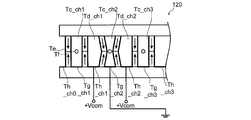
- FIG. 3A to 3C are side sectional views showing an example of the configuration of the head main body 120.
- FIG. 3A to 3C correspond to cross-sectional views of the head main body 120 of FIG. 2 cut at the position FF.
- the head body 120 is provided with first electrodes Tg_ch1 to Tg_ch128 and second electrodes Th_ch0 to Th_ch128 (not shown in FIG. 2) in order to individually drive the ink channels Tc_ch1 to Tc_ch128.
- the first electrodes Tg_ch1 to Tg_ch128 and the second electrodes Th_ch0 to Th_ch128 are electrode pairs formed on the side surfaces of the ink channels Tc_ch1 to Tc_ch128 and the air channels Td_ch1 to Td_ch127 so as to face each other with the drive wall Te interposed therebetween. That is, the drive wall Te, the first electrode Tg, and the second electrode Th constitute a piezoelectric element for driving one ink channel Tc.
- the first electrodes Tg_ch1 to Tg_ch128 are formed on the side surfaces of the ink channels Tc_ch1 to Tc_ch128 so as to straddle both the piezoelectric member Ta and the piezoelectric member Tb.
- Each of the first electrodes Tg_ch1 to Tg_ch128 is formed so as to be electrically separated from each other, and individually connected to a driver IC 110A (described later with reference to FIG. 4) of the driving unit 110 (hereinafter, referred to as “wireless connection”). Also referred to as “individual electrode Tg”).
- the individual electrodes Tg_ch1 to Tg_ch128 are individually supplied with voltage by the driver IC 110A.
- the second electrodes Th_ch0 to Th_ch128 are formed on the side surfaces of the air channels Td_ch1 to Td_ch127 so as to straddle both the piezoelectric member Ta and the piezoelectric member Tb.
- the second electrodes Th_ch0 to Th_ch128 are electrically connected to each other, and are connected to a COM driver 110B (described later with reference to FIG. 4) of the driving unit 110 by a common wiring (hereinafter referred to as “common electrode Th”). ").
- the common electrodes Th_ch0 to Th_ch128 are commonly supplied with voltage by the COM driver 110B.
- FIG. 3A to 3C show basic operations of the shear mode type ink jet head 100, respectively.
- FIG. 3A shows a state in which the drive wall Te is not sheared
- FIGS. 3B and 3C show the drive wall Te. Represents the state of bending (shear deformation).
- the driving unit 110 supplies a voltage to each of the individual electrode Tg and the common electrode Th so that a potential difference is generated between the individual electrode Tg and the common electrode Th.
- the drive wall Te of the piezoelectric member bends around the adhesive portion between the piezoelectric member Ta and the piezoelectric member Tb according to the applied voltage.
- the volume of the ink channel Tc changes due to the bending of the drive wall Te of the piezoelectric member, and ink is ejected from the nozzle Tf.
- the driving unit 110 When ejecting ink from the ink channel Tc_ch2, the driving unit 110 first supplies the + VH2 voltage to the individual electrode Tg_ch2, and supplies the reference voltage (GND) to the common electrodes Th_ch1 and Th_ch2, as shown in FIG. 3B, for example. As a result, the drive wall Te is shear-deformed to expand the volume of the ink channel Tc_ch2.
- the driving unit 110 supplies the reference voltage (GND) to the individual electrode Tg_ch2, and supplies the + Vcom voltage ( ⁇ + VH2) to the common electrodes Th_ch1 and Th_ch2, thereby driving the driving wall Te.
- Shear deformation is performed to shrink the volume of the ink channel Tc_ch2.
- high pressure is applied to the ink in the ink channel Tc_ch2, and the ink is ejected from the nozzle Tf.
- the inkjet head 100 forms separate piezoelectric elements on the wall portions Te of the ink channels Tc_ch1 to Tc_ch128 by the individual electrodes Tg_ch1 to Tg_ch128 and the common electrodes Th_ch0 to Th_ch128. Each ink channel Tc_ch1 to Tc_ch128 is individually driven.
- FIG. 4 is a diagram illustrating an example of the configuration of the drive unit 110.
- the drive unit 110 includes a driver IC 110A (corresponding to the “first drive circuit” of the present invention) and a COM driver 110B (corresponding to the “second drive circuit” of the present invention). Is done.
- the driver IC 110A generates drive voltages to be supplied to the individual electrodes Tg_ch1 to Tg_ch128 of the ink channels Tc_ch1 to Tc_ch128, and supplies the drive voltages to the individual electrodes Tg_ch1 to Tg_ch128 separately.
- the COM driver 110B generates a common voltage to be supplied to the common electrodes Th_ch0 to Th_ch128 of each ink channel Tc_ch1 to Tc_ch128, and supplies the common voltage to the common electrodes Th_ch0 to Th_ch128 in common.
- the driver IC 110A and the COM driver 110B operate in synchronization with each other in accordance with a drive signal output from the drive signal generation circuit 18 (that is, a signal for instructing the timing of expansion and contraction of the ink channel Tc) (see FIG. 12). See later).
- a drive signal output from the drive signal generation circuit 18 that is, a signal for instructing the timing of expansion and contraction of the ink channel Tc
- the driver IC 110A includes a fixed value data removal circuit 111, a shift register 112, a latch circuit 113, a gray scale controller 114, and a buffer amplifier 115.
- the fixed value data removal circuit 111 causes the shift register 112 to acquire only the image data INPUT_DATA2 from which zero fill data is thinned out of the image data INPUT_DATA transferred from the line memory 16.
- FIG. 5A, 5B, 6A, and 6B are diagrams for explaining the function of the fixed value data removal circuit 111.
- FIG. 5A, 5B, 6A, and 6B are diagrams for explaining the function of the fixed value data removal circuit 111.
- 5A and 5B show a mode of data transfer from the main body 2 to the driver ICP 110 in the inkjet head P100 according to the prior art.
- 6A and 6B show a mode of data transfer from the main body 2 to the driver IC 110 in the inkjet head 100 according to the present embodiment.
- the image data INPUT_DATA transferred from the line memory 16 of the main body 2 to the driver IC (P110 or 110) is usually “pixel data” for each bit in the order of the address of the pixel area. ”(That is, 1-bit data indicating“ 0 ”or“ 1 ”) and“ zero fill data ”(that is, 1-bit data indicating“ 0 ”) are alternately arranged.
- the image data INPUT_DATA is, for example, in order of pixel data D255 at address 255, zero fill data, pixel data D254 at address 254, zero fill data, pixel data D253 at address 253, and so on, for each bit.
- the data is transferred in synchronization with the transfer clock signal INPUT_CLK.
- the driver IC receives from the main body 2 a transfer clock signal (hereinafter referred to as “first transfer clock signal”) INPUT_CLK of the image data INPUT_DATA together with the image data INPUT_DATA.
- first transfer clock signal a transfer clock signal
- the “pixel data” is the gradation data for each pixel region in the “image data”, and the ink discharge amount that each ink channel Tc_ch1 to Tc_ch128 of the head body 120 discharges in one pixel region. It corresponds to.
- the driver IC (P110 or 110) determines drive voltages to be supplied to the individual electrodes Tg_ch1 to Tg_ch128 provided in the ink channels Tc_ch1 to Tc_ch128, based on “pixel data”.
- Zero fill data (hereinafter also referred to as “fixed value data”) is data input to synchronize the voltage supply timing to the common electrodes Th_ch0 to Th_ch128 with the voltage supply timing to the individual electrodes Tg_ch1 to Tg_ch128.
- a fixed value such as “0” is set.
- the shift register in the driver ICP110 is an image including both “pixel data” and “zero fill data” in synchronization with the first transfer clock signal INPUT_CLK. Acquiring data INPUT_DATA. For this reason, when the data transfer rate to the shift register (that is, the clock frequency of the first transfer clock signal INPUT_CLK) is increased, a transfer failure or the like may occur.
- the fixed value data removal circuit 111 is interposed between the line memory 16 and the shift register 112, for example, and acquires image data INPUT_DATA transferred from the line memory 16 in synchronization with the first transfer clock signal INPUT_CLK. Then, the fixed value data removal circuit 111 transfers only the image data INPUT_DATA2 of either the even address or the odd address of the acquired image data INPUT_DATA, and the transfer clock signal (1/2) of the first transfer clock signal INPUT_CLK. The data is transferred to the shift register 112 in synchronization with INPUT_CLK2 (hereinafter referred to as “second transfer clock signal”).
- the fixed value data removal circuit 111 causes the shift register 112 to acquire only the pixel data INPUT_DATA2 from which zero fill data has been thinned out of the image data INPUT_DATA transferred from the line memory 16. In other words, this halves the amount of data transferred to the shift register 112 and reduces the operating speed of the shift register 112.
- an SRAM (hereinafter also referred to as a dual port SRAM) configured to be able to simultaneously execute an image data writing operation and an image data reading operation, or a frequency dividing circuit. (Described later in the second embodiment) can be applied.
- FIG. 7A is a diagram showing an example of the configuration of the fixed value data removal circuit 111 according to the present embodiment.
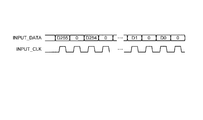
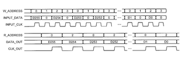
- FIG. 7B is a timing chart showing an example of a sequence of a write operation and a read operation in the fixed value data removal circuit 111.
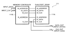
- the fixed value data removal circuit 111 includes, for example, a dual port SRAM 111A and a memory controller 111B.
- the memory controller 111B is provided to control the operation of the dual port SRAM 111A.
- INPUT_DATA image data input from the line memory 16 (D255, D254, D253, D252... D1, D0 represent pixel data of the corresponding address)
- W_ADRESS Write address command to dual port SRAM 111A
- INPUT_CLK First transfer clock signal input from line memory 16
- R_ADRESS Read address command from dual port SRAM 111A DATA_OUT (INPUT_DATA2): Output from dual port SRAM 111A to shift register 112
- Image data D255, D254, D253, D252 ... D1, D0 represent pixel data of the corresponding address
- CLK_OUT (INPUT_CLK2): the second transfer clock signal output from the dual port SRAM 111A to the shift register 112
- the memory controller 111B acquires the image data INPUT_DATA transferred from the line memory 16 in synchronization with the first transfer clock signal INPUT_CLK. Then, the memory controller 111B sequentially transfers the image data INPUT_DATA to the data writing input terminal WDATA of the dual port SRAM 111A. The memory controller 111B sequentially transfers the first transfer clock signal INPUT_CLK to the write clock signal input terminal WCLK of the dual port SRAM 111A.
- the memory controller 111B sequentially issues an address increment command in the dual port SRAM 111A to which the image data INPUT_DATA is written to the input terminal W_ADDRESS for the write address of the dual port SRAM 111A in synchronization with the first transfer clock signal INPUT_CLK. Output.
- the memory controller 111B generates a second transfer clock signal INPUT_CLK2 obtained by dividing the first transfer clock signal INPUT_CLK by 1/2, and uses the second transfer clock signal INPUT_CLK2 as an input terminal RCLK for the read clock signal of the dual port SRAM 111A.
- the memory controller 111B reads out the address increment command in the dual port SRAM 111A from which the image data INPUT_DATA2 is read out, for the read address of the dual port SRAM 111A in synchronization with the second transfer clock signal INPUT_CLK in a state where odd addresses are thinned out. Output sequentially to input terminal R_ADDRESS.
- the memory controller 111B performs control so that only data at an even address (or odd address) of image data INPUT_DATA written to the dual port SRAM 111A is read from the dual port SRAM 111A.
- the dual port SRAM 111A sequentially acquires the image data INPUT_DATA transferred from the memory controller 111B in synchronization with the first transfer clock signal INPUT_CLK, and addresses “0”, “1”, “2”, “3”. Store sequentially at one of the addresses. Then, the dual port SRAM 111A reads only the even-numbered image data among the image data stored in itself and shifts only the “pixel data” INPUT_DATA2 in which the zero fill data is thinned out in synchronization with the second transfer clock signal INPUT_CLK2. Output to the register 112.
- the dual port SRAM 111A executes the write operation and the read operation simultaneously.
- the shift register 112 stores pixel data INPUT_DATA2 of the image data INPUT_DATA transferred from the main body 2 in association with each of the plurality of ink channels Tc_ch1 to Tc_ch128.
- the shift register 112 is constituted by, for example, a FIFO type memory that stores pixel data for 128 ink channels Tc_ch1 to Tc_ch128 (for example, data of 3 bits ⁇ 128 ink channels).
- the image data INPUT_DATA2 and the second transfer clock signal INPUT_CLK2 are input from the fixed value data removal circuit 111 to the shift register 112 according to the present embodiment.
- the shift register 112 sequentially acquires 3-bit pixel data sequentially transferred from the fixed value data removal circuit 111 via the three signal lines in synchronization with the second transfer clock signal INPUT_CLK2.
- each pixel data INPUT_DATA2 included in the image data INPUT_DATA transferred from the main body 2 is stored 128 pieces in the order of input to the shift register 112.
- the 3 ⁇ 128-bit image data stored in the shift register 112 is collectively output as parallel data to the latch circuit 113 in response to the latch signal LAT.
- the latch circuit 113 holds the image data output from the shift register 112 (here, 3-bit pixel data for 128 ink channels) and outputs it to the grayscale controller 114. Then, the latch circuit 113 resets the held image data in response to the latch signal LAT, and acquires new image data from the shift register 112.
- the gray scale controller 114 determines a drive voltage pattern to be supplied to each individual electrode Tg_ch1 to Tg_ch 128 based on the image data output from the latch circuit 113, and outputs a drive signal corresponding to the drive voltage pattern.
- the data is output to the buffer amplifier 115.
- FIG. 8 is a diagram illustrating an example of a conversion table of pixel data and drive waveform pattern data referred to by the gray scale controller 114.
- FIG. 9 is a diagram showing three types of drive waveforms in the drive waveform pattern data of FIG.
- FIG. 10 and 11 are diagrams showing examples of output waveforms output from the buffer amplifier 115 to the individual electrodes Tg based on the drive signal of the grayscale controller 114.
- FIG. 10 and 11 are diagrams showing examples of output waveforms output from the buffer amplifier 115 to the individual electrodes Tg based on the drive signal of the grayscale controller 114.
- the pixel data (3 ⁇ 128 bit data) for 128 ink channels Tc_ch1 to Tc_ch128 is input in parallel to the gray scale controller 114 from the latch circuit 113. Further, the grayscale controller 114 receives three types of drive signals (a drive signal pulse_timing0 including a non-discharge waveform, a drive signal pulse_timing1 including a non-operation waveform, and a drive signal pulse_timing2 including a discharge waveform) from the drive signal generation circuit 18. 3 types) are input.
- the gray scale controller 114 converts each pixel data of 128 ink channels Tc_ch1 to Tc_ch128 (3 ⁇ 128 bit data) output in parallel from the latch circuit 113 into drive waveform pattern data. Then, the gray scale controller 114 selectively connects the drive signals defined in the drive waveform pattern data among the three types of drive signals input from the drive signal generation circuit 18 to each of the 128 ink channels Tc_ch1 to Tc_ch128. Is output to the buffer amplifier 115.
- the gray scale controller 114 acquires the synchronous clock signal GSCLK and the reset signal RST from the control circuit 17 and outputs a drive signal to the buffer amplifier 115 in accordance with the timing of the synchronous clock signal GSCLK and the reset signal RST. Switching.
- pixel data of 3 bits (0, 0, 0) to (1, 1, 1) is converted into 8 drive waveforms within 8 counts of the gray scale count GSC (0 to 7).
- the drive waveform within each count of the drive waveform pattern can take three values “0”, “1”, and “2”.
- the drive waveform pattern data of (1, 1, 2, 2, 2, 2, 2, 0) is selected for the pixel data (1, 0, 1).
- the conversion table in FIG. 8 is stored in a register (not shown) built in the gray scale controller 114, for example.
- the gray scale count GSC (0 to 7) is counted by a counter (not shown) built in the gray scale controller 114 based on the synchronous clock signal GSCLK input from the control circuit 17.
- the three types of drive signals are digital data indicating temporal changes between binary values of high level and low level (see FIG. 9).
- the drive signal pulse_timing0 is a signal that is maintained at a low level for a period of one count of the grayscale count GSC, and corresponds to a non-ejection waveform.
- the drive signal pulse_timing2 is a signal that is at a high level for a predetermined period in a period corresponding to one count of the grayscale count GSC, and corresponds to an ejection waveform.
- the drive signal pulse_timing1 is a signal that becomes a high level for a predetermined period after the drive signal pulse_timing2 returns to a low level in a period corresponding to one count of the grayscale count GSC, and corresponds to a non-operation waveform.
- the drive signals pulse_timing1 and pulse_timing2 are generated in synchronization with the synchronous clock signal GSCLK so that one pulse can be output within a period of one count of the grayscale count GSC.
- the drive signals are selected in the order of pulse_timing0, pulse_timing2, pulse_timing2, pulse_timing2, pulse_timing2, pulse_timing2, pulse_timing1, pulse_timing1, and a drive waveform pattern in which the corresponding drive signals are connected is generated (see FIG. 11).
- the gray scale controller 114 selects any one of these three types of drive signals based on the drive waveform pattern data, and outputs the selected drive signal to the buffer amplifier 115.
- the buffer amplifier 115 supplies a drive voltage to each of the individual electrodes Tg_ch1 to Tg_ch128 based on the drive signal input from the grayscale controller 114.
- the buffer amplifier 115 is individually provided so as to correspond to each of the 128 ink channels Tc_ch1 to Tc_ch128 so that a drive voltage can be individually supplied to each of the individual electrodes Tg_ch1 to Tg_ch128 of the 128 ink channels Tc_ch1 to Tc_ch128. .
- the buffer amplifier 115 supplies the voltage + VH2 to the individual electrode Tg during a period when the drive signal pulse_timing2 including the ejection waveform is at a high level. Further, the buffer amplifier 115 supplies a voltage + VH1 smaller than the voltage + VH2 to the individual electrode Tg during a period in which the drive signal pulse_timing1 including the non-operation waveform is at a high level. Further, the buffer amplifier 115 supplies the GND voltage to the individual electrode Tg during the period when both of the drive signals pulse_timing1 and pulse_timing2 are at the low level and during the period when the drive signal pulse_timing0 is selected.
- FIG. 12 is a diagram illustrating an example of the configuration of the buffer amplifier 115 and the COM driver 110B. Note that TM in FIG. 12 is a piezoelectric element formed on both side surfaces of one ink channel Tc.
- the buffer amplifier 115 includes, for example, a first transistor 115a, a second transistor 115b, and a third transistor 115c.
- the voltage + VH2 is input from the first power supply, and the voltage + VH1 lower than the voltage + VH2 is input from the second power supply.
- the buffer amplifier 115 Based on the drive signal (drive signal pulse_timing0, drive signal pulse_timing1, or drive signal pulse_timing2) input from the grayscale controller 114, the buffer amplifier 115 performs the first transistor 115a, the second transistor 115b, or the third transistor Any one of the transistors 115c is operated to supply one of the output voltages of the voltage + VH1, the voltage + VH2, and the GND voltage to the individual electrode Tg of the piezoelectric element TM.
- the first transistor 115a is, for example, an N-type MOSFET having a drain terminal connected to a power supply of voltage + VH2, and a source terminal connected to an individual electrode Tg.
- a drive signal corresponding to the drive signal pulse_timing2 is input from the grayscale controller 114 to the gate terminal of the first transistor 115a.
- the second transistor 115b is, for example, an N-type MOSFET having a drain terminal connected to a power source having a voltage + VH1 and a source terminal connected to an individual electrode Tg.
- a drive signal corresponding to the drive signal pulse_timing1 is input from the grayscale controller 114 to the gate terminal of the second transistor 115b.
- the third transistor 115c is, for example, an N-type MOSFET in which the source terminal is grounded and the individual electrode Tg is connected to the drain terminal.
- a drive signal corresponding to the drive signal pulse_timing0 is input from the grayscale controller 114 to the gate terminal of the third transistor 115c.
- the buffer amplifier 115 supplies the GND voltage to the individual electrode Tg of the piezoelectric element TM when the drive signal pulse_timing0 is at a high level, and supplies the voltage + VH1 to the individual electrode Tg of the piezoelectric element TM when the drive signal pulse_timing1 is at a high level.
- the voltage + VH2 is supplied to the individual electrode Tg of the piezoelectric element TM while the drive signal pulse_timing2 is at a high level.
- the COM driver 110B supplies a common voltage to the common electrodes Th_ch0 to Th_ch128 at the timing of contracting the ink channel Tc. That is, in the COM driver 110B, after the driver IC 110A supplies a drive voltage (here, voltage + VH2) to the individual electrode Tg to expand the ink channel Tc (see FIG. 3B), the ink channel Tc is In order to contract, a common voltage is supplied to the common electrode Th. As a result, a voltage opposite to the drive voltage is supplied to the drive wall Te, and ejection from the ink channel Tc is executed (see FIG. 3C).
- a drive voltage here, voltage + VH2
- the drive signal pulse_timing1 is input from the drive signal generation circuit 18, and the voltage + Vcom is input from the power source.
- the COM driver 110B supplies the common voltage + Vcom to the common electrodes Th_ch0 to Th_ch128 in response to the drive signal pulse_timing1. That is, the COM driver 110B supplies the common voltage + Vcom to the common electrodes Th_ch0 to Th_ch128 at the timing of the drive signal pulse_timing1 subsequent to the drive signal pulse_timing2 within a period corresponding to one count of the grayscale count GSC.
- the ink channel Tc operates to perform ink ejection by contracting immediately after expansion within a period of one count of the gray scale count GSC during the ejection operation.
- the “common voltage” is not particularly limited in the present invention.
- the common voltage is set to the same voltage as the driving voltage + VH1 supplied to the individual electrode Tg when the driver IC 110A is not operating (a period in which the driving signal pulse_timing1 is at a high level). Is set.
- the ink discharge pressure in the ink channel Tc is in a steady state without increasing until the ink channel Tc expands again after the ink channel Tc contracts once. That is, in the ink channel Tc according to the present embodiment, after the drive voltage is supplied from the individual electrode Tg while the drive signal pulse_timing2 is at the high level, the drive signal pulse_timing1 becomes the high level and the common voltage is applied to the common electrode Th. Ink is ejected only at the timing immediately after the ink is supplied.
- the COM driver 110B includes, for example, a fourth transistor 110Ba and a fifth transistor 110Bb.
- the COM driver 110B operates either the fourth transistor 110Ba or the fifth transistor 110Bb based on the drive signal (here, the drive signal pulse_timing1) input from the drive signal generation circuit 18, and the common voltage + Vcom Alternatively, any output voltage of the GND voltage is supplied to the common electrode Th of the piezoelectric element TM.
- the fourth transistor 110Ba is, for example, an N-type MOSFET having a drain terminal connected to a power supply having a voltage + Vcom and a source terminal connected to a common electrode Th.
- the fifth transistor 110Bb is, for example, a P-type MOSFET having a source terminal grounded and a drain terminal connected to the common electrode Th.
- the drive signal pulse_timing1 is input to the gate terminals of the fourth transistor 110Ba and the fifth transistor 110Bb.
- the COM driver 110B supplies the common voltage + Vcom to the common electrode Th of the piezoelectric element TM when the drive signal pulse_timing1 is at a high level, and supplies the GND voltage to the common electrode Th during other periods. .
- the inkjet head 100 controls the voltage supplied to the piezoelectric elements of the ink channels Tc_ch1 to Tc_ch128 by the driver IC 110A and the COM driver 110B, unlike the inkjet head according to the related art. Since the COM driver 110B is typically configured on a circuit board separate from the driver IC 110A, a low output impedance can be realized.
- FIG. 13A FIG. 13B, FIG. 14, and FIG.
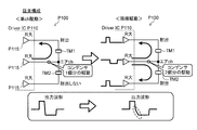
- FIG. 13A shows an operation in the case where only one piezoelectric element TM1 is driven (left figure) and when two adjacent piezoelectric elements TM1 and TM2 are driven simultaneously (right figure) in the inkjet head P100 according to the prior art. It is a figure which shows the difference.
- FIG. 13B shows a case in which only one piezoelectric element TM1 is driven (left figure) and two adjacent piezoelectric elements TM1 and TM2 are driven simultaneously (right figure) in the inkjet head 100 according to the present embodiment. It is a figure which shows the difference in operation
- the drive voltage is supplied to the individual electrode Tg using only the driver ICP110, and the common voltage is supplied to the common electrode Th. It has become.
- the output impedance of the buffer amplifier P115 is generally increased due to chip size restrictions and the like.
- the magnitude of the output impedance of the buffer amplifier P115 becomes a problem particularly in the buffer amplifier P115 that supplies a common voltage to the common electrode Th.
- the number of piezoelectric elements to be driven changes with time in both the conventional configuration and the configuration of the present application.
- the number of piezoelectric elements to which a common voltage is supplied to the common electrode Th varies with time.
- the driver ICP 110 since the output impedance of the buffer amplifier P115 is large, the driver ICP 110 is easily affected by the number of piezoelectric elements to which a common voltage is supplied. That is, in the driver ICP 110 according to the conventional configuration, when the number of piezoelectric elements to be driven increases, as shown in the right diagram of FIG. 13A, when the common voltage is supplied to the common electrode Th, the buffer There is a possibility that an operational delay (RC delay) of the amplifier P115 occurs, and an output waveform supplied from the buffer amplifier P115 to the common electrode Th may be lost (also referred to as adjacent channel crosstalk). When such adjacent channel crosstalk occurs, a delay in the timing of ejecting ink from the ink channel Tc occurs.
- RC delay operational delay
- the driver ICP 110 when increasing the number of piezoelectric elements to be driven, even when the piezoelectric elements to be driven are not adjacent to each other, the output waveform is distorted as in the case of adjacent channel crosstalk. A delay in the timing of ejecting ink occurs. As a result, if the number of piezoelectric elements to be driven is decreased after increasing the number of piezoelectric elements to be driven, the ink discharge interval is widened in the area between them, and an area where ink cannot be discharged is generated (load crosstalk). Also called).
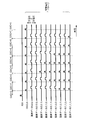
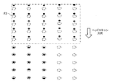
- FIG. 14 is a diagram illustrating an example of a state in which adjacent channel crosstalk has occurred in the inkjet head P100 according to the related art.
- FIG. 15 is a diagram illustrating an example of a state in which load channel crosstalk has occurred in the inkjet head P100 according to the related art.
- 14 and 15 show a state in which the ink jet head P100 simultaneously ejects ink from each of the five nozzles while moving in the head scan direction.
- the arrow direction indicates the head scanning direction of the inkjet head
- the dotted line area indicates the target discharge position for each nozzle
- the dot area indicates the actual discharge position for each nozzle.
- the ejection position of the ink ejected from the leftmost nozzle (area F1 surrounded by the alternate long and short dash line) is greater than the ejection position of the ink ejected from the other nozzles. Also, it is in a state shifted to the opposite side to the head scanning direction.
- the displacement of the ink ejection position occurs due to the adjacent channel crosstalk and the load crosstalk, which causes deterioration of the image quality.
- the inkjet head 100 is configured to supply a common voltage to the common electrode Th by using a COM driver 110B separate from the driver IC 110A.
- the on-resistance can be reduced as compared with the transistor of the driver IC 110A.
- the output impedance of the COM driver 110B with respect to the piezoelectric element can typically be reduced to 1/1000 or less of the output impedance of the driver IC 110A with respect to the piezoelectric element.
- the inkjet head 100 stores the image data transferred from the main body 2 of the image forming apparatus 1 in the shift register 112, and a plurality of ink channels Tc_ch1 based on the image data.
- Driver IC (first drive circuit) 110A that individually supplies a drive voltage to one electrode (individual electrode) Tg of each piezoelectric element TM of each of Tc_ch 128 and each of the plurality of ink channels Tc_ch1 to Tc_ch 128
- a COM driver (second drive circuit) 110B that supplies a common voltage to the plurality of ink channels Tc_ch1 to Tc_ch128 with respect to the other electrode (common electrode) Th of the TM is provided.
- the driver IC 110A has fixed value data out of image data INPUT_DATA in which pixel data and fixed value data are alternately arranged for each bit transferred from the main body 2.
- a fixed value data removal circuit 111 that relays between the main body 2 and the shift register 112 so that only the pixel data INPUT_DATA2 obtained by thinning out is sequentially stored in the shift register 112.
- the driver IC 110A and the COM driver 110B In addition, it is configured to operate synchronously according to predetermined timing command signals (for example, drive signals pulse_timing0, pulse_timing1, pulse_timing2).
- the image data transfer is performed in a format in which the existing image data transfer method (that is, pixel data and fixed value data are alternately arranged for each bit).
- the operation speed of the shift register 112 of the driver IC 110A can be reduced while maintaining compatibility with the system. As a result, it is possible to suppress the failure of data transfer in the shift register 112 of the driver IC 110A. This also makes it possible to increase the data transfer speed of the pixel data to the shift register 112 of the driver IC 110A.
- the inkjet head 100 can be configured to supply a common voltage to the common electrode Th of the piezoelectric element TM by a COM driver 110B separate from the driver IC 110A. It is possible to reduce the output impedance (for example, on-resistance) with respect to the piezoelectric element TM. Typically, with this configuration, the output impedance of the COM driver 110B with respect to the piezoelectric element TM can be reduced to 1/1000 or less of the output impedance of the driver IC 110A with respect to the piezoelectric element TM. As a result, the occurrence of adjacent channel crosstalk and load crosstalk can be suppressed.
- a COM driver 110B separate from the driver IC 110A.
- the fixed value data removal circuit 111 acquires image data that is data-transferred from the main body 2 in synchronization with the first transfer clock signal INPUT_CLK by the dual port SRAM 110B and the like, and the shift register 112.
- the pixel data INPUT_DATA2 is transferred in synchronization with the second transfer clock signal INPUT_CLK2 obtained by dividing the first transfer clock signal INPUT_CLK by 1/2. Accordingly, since the second transfer clock signal INPUT_CLK2 and the image data INPUT_DATA2 are synchronized with each other and transferred to the subsequent shift register 112 or the like, high noise resistance can be realized.
- the fixed value data removal circuit 111 relays both the image data INPUT_DATA and the first transfer clock signal INPUT_CLK from which data is transferred from the main body 2 to the shift register 112.
- the inkjet head 100 according to the present embodiment is different from the first embodiment in that only the first transfer clock signal INPUT_CLK input from the main body 2 is relayed. Note that description of configurations common to the first embodiment is omitted.
- FIG. 16 is a diagram illustrating an example of the configuration of the drive unit 110 of the inkjet head 100 according to the present embodiment.
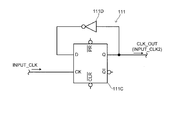
- FIG. 17A is a diagram illustrating an example of the configuration of the fixed value data removal circuit 111 according to the present embodiment.
- FIG. 17B is a timing chart during operation of the fixed value data removal circuit 111 according to the present embodiment.
- the fixed value data removal circuit 111 obtains the first transfer clock signal INPUT_CLK2 of the image data INPUT_DATA input from the main body 2 and the second transfer clock signal INPUT_CLK2 obtained by dividing the first transfer clock signal INPUT_CLK by 1/2. It is comprised by the frequency divider circuit which produces
- the mask process using the second transfer clock signal INPUT_CLK2 may be an aspect in which the input of the edge trigger signal of the shift register 112 is the second transfer clock signal INPUT_CLK2 as shown in FIG.
- An aspect using an AND circuit or the like may be used.
- the D flip-flop 111C and the inverter circuit 111D constitute a frequency dividing circuit.
- INPUT_DATA Image data input from the line memory 16 to the shift register 112 (D255, D254, D253, D252... D1, D0 represent pixel data of the corresponding address)
- INPUT_CLK first transfer clock signal input from the line memory 16 to the D flip-flop 111C
- CLK_OUT second transfer clock signal output from the D flip-flop 111C to the shift register 112
- the first transfer clock signal INPUT_CLK from the main body 2 is input to the clock input terminal CK of the D flip-flop 111C.
- An inverter circuit 111D is provided between the data input terminal D and the data output terminal Q of the D flip-flop 111C, and the output of the data output terminal Q is inverted and returned to the data input terminal D. .
- the D flip-flop 111C holds the inverted signal of the data output terminal Q at the timing of the rising edge of the first transfer clock signal INPUT_CLK.
- the second transfer clock signal INPUT_CLK2 obtained by dividing the first transfer clock signal INPUT_CLK by 1/2 is output from the data output terminal Q of the D flip-flop 111C.
- the second transfer clock signal INPUT_CLK2 is input as an edge trigger signal of the shift register 112.
- the shift register 112 acquires image data INPUT_DATA to which data is transferred from the main body 2 in synchronization with the first transfer clock signal INPUT_CLK in synchronization with the second transfer clock signal INPUT_CLK2. That is, the shift register 112 stores only the data of either the even address or the odd address of the image data INPUT_DATA transferred from the main body 2, that is, only the pixel data.
- the inkjet head 100 is useful in that the fixed value data removal circuit 111 can be realized with a simple configuration.
- the fixed value data removal circuit 111 converts the asynchronous image data INPUT_DATA and the second transfer clock signal INPUT_CLK2 into the shift register 112. Therefore, it is more fragile than the fixed value data removal circuit 111 according to the first embodiment in terms of noise resistance. Therefore, it is desirable to study the circuit configuration of the fixed value data removal circuit 111 in view of both simplification of the circuit configuration and noise resistance.
- the fixed value data removal circuit 111 As an example of the fixed value data removal circuit 111, a mode in which fixed value data is always thinned out is shown. However, as a configuration of the fixed value data removal circuit 111, more preferably, the first data is transferred to the shift register 112 only at either the even address or the odd address among the acquired image data INPUT_DATA. And the second mode in which data of both the even address and the odd address in the acquired image data INPUT_DATA are transferred to the shift register 112 selectively. Thus, the present invention can be applied even when the main body 2 has a device configuration for transferring image data that does not include fixed value data.
- the fixed value data removal circuit 111 is built in the driver IC 110A.
- the fixed value data removal circuit 111 may be formed on a substrate separate from the driver IC 110A.
- the driver IC 110A stores the image data transferred from the main body 2 of the image forming apparatus in the shift register 112, and based on the image data, the individual piezoelectric elements of each of the plurality of ink channels Tc are stored. If the circuit configuration is such that the drive voltage is individually supplied to the electrodes and the COM driver 110B supplies the common voltage to the common electrode of each of the plurality of ink channels Tc, Various changes can be made. Typically, the driver IC 110A and the COM driver 110B only need to operate in synchronization based on a signal that commands the timing of expansion and contraction of the ink channel Tc.
- a mode is shown in which all 128 piezoelectric elements configured in the ink channels Tc_ch1 to Tc_ch128 of the head main body 120 are used. It was. However, instead of this aspect, a voltage may be supplied to 128 piezoelectric elements by a plurality of COM drivers 110B.
- a shear mode type ink jet head is shown as an example of the ink jet head 100.
- the present invention can also be applied to types of inkjet heads other than the shear mode inkjet head, such as a radial mode inkjet head.
- the inkjet head according to the present disclosure is suitable for realizing high image quality of printing images and high-speed printing.
Landscapes
- Particle Formation And Scattering Control In Inkjet Printers (AREA)
Abstract
圧電素子を構成する壁部で各別に区画された複数のインクチャネル(Tc)を有し、複数のインクチャネル(Tc)を、当該複数のインクチャネル(Tc)それぞれの圧電素子への電圧供給によって各別に駆動するインクジェットヘッド(100)であって、画像形成装置(1)の本体(2)からデータ転送される1ビット毎に画素データと固定値データとが交互に配列された画像データのうちの固定値データを間引いた画素データのみが、シフトレジスター(112)に順番に記憶されるように、本体(2)とシフトレジスター(112)の間を中継する固定値データ除去回路(111)を有している。
Description
本開示は、インクジェットヘッド、及び画像形成装置に関する。
従来、圧電素子を構成する壁部で各別に区画された複数のインクチャネルを有し、当該複数のインクチャネルを、当該複数のインクチャネルそれぞれの圧電素子への電圧供給によって各別に駆動するインクジェットヘッドが知られている(例えば、特許文献1を参照)。
この種のインクジェットヘッドとしては、例えば、シアモード型圧電素子を用いたインクジェットヘッド(シアモード型インクジェットヘッドとも称される)が知られている。シアモード型インクジェットヘッドは、圧電部材たる壁部(以下、「駆動壁」と称する)を挟んで、インク吐出を行う圧力室(以下、「インクチャネル」と称する)とインク吐出を行わない空気室(以下、「エアチャネル」と称する)とが交互に配設された構造を有している。当該インクジェットヘッドにおいては、駆動壁の両側面に、インクチャネル内に当該駆動壁に電圧を印加する一方側の電極が配設され、エアチャネル内に当該駆動壁に電圧を印加する他方側の電極が配設され、これによって、圧電素子が構成されている。そして、当該インクジェットヘッドは、当該駆動壁の両側面に配設した当該一対の電極に電圧を印加することにより、当該駆動壁をせん断変形させ、インクチャネル内のインクをノズルから吐出する(図3A、図3B、図3Cを参照して後述)。
従来、この種のインクジェットヘッドは、ドライバーICによって、複数のインクチャネルそれぞれの圧電素子に対して、個別に、電圧供給の制御を行っており、これにより、複数のインクチャネルそれぞれを独立に駆動している。
当該ドライバーICは、通常、一のインクチャネルを駆動制御する際には、インクチャネルを膨張させるタイミングで圧電素子の一方の電極(例えば、インクチャネル内に配設された電極)に対して個別に、画像データに応じた駆動電圧を供給し、又、インクチャネルを収縮させるタイミングで圧電素子の他方の電極(例えば、エアチャネル内に配設された電極)に対して基準電圧を供給する構成となっている。そのため、画像形成装置の本体から、ドライバーIC内のシフトレジスターに対しては、画素領域のアドレス順に、1ビット毎に、一方の電極に対応する画素データと他方の電極に対応するゼロフィルデータ(即ち、ダミーデータ)とが交互に配列された画像データが、シリアルにデータ転送される構成となっている(図5を参照して後述)。
ところで、この種の画像形成装置においては、印刷画像の高画質化及び印刷の高速化等の要請から、圧電素子に対して電圧供給を行うドライバーICの高速動作が求められている。
この点、特許文献1等の従来技術においては、ドライバーICの高速動作を実行しようとした場合、ドライバーIC内のシフトレジスターに対するデータ転送の失敗や、ドライバーICから圧電素子に対して電圧供給する際の出力波形のなまり等が生じるおそれがあった。そして、かかるデータ転送の失敗や出力波形のなまりに起因して、例えば、インクの吐出位置や吐出量にずれが生じ、印刷画像の画質が劣化するおそれがあった。
本開示は、上記問題点に鑑みてなされたもので、印刷画像の高画質化及び印刷の高速化等の実現により好適なインクジェットヘッド、及び画像形成装置を提供することを目的とする。
前述した課題を解決する主たる本開示は、
圧電素子を構成する壁部で各別に区画された複数のインクチャネルを有し、前記複数のインクチャネルを、当該複数のインクチャネルそれぞれの前記圧電素子への電圧供給によって各別に駆動するインクジェットヘッドであって、
画像形成装置の本体からデータ転送される画像データをシフトレジスターに記憶して、当該画像データに基づいて、前記複数のインクチャネルそれぞれの前記圧電素子の一方の電極に対して、個別に駆動電圧を供給する第1の駆動回路と、
前記複数のインクチャネルそれぞれの前記圧電素子の他方の電極に対して、前記複数のインクチャネルに共通のコモン電圧を供給する第2の駆動回路と、
を備え、
前記第1の駆動回路は、前記本体からデータ転送される1ビット毎に画素データと固定値データとが交互に配列された前記画像データのうちの前記固定値データを間引いた前記画素データのみが、前記シフトレジスターに順番に記憶されるように、前記本体と前記シフトレジスターの間を中継する固定値データ除去回路を有し、
前記第1の駆動回路と前記第2の駆動回路とは、所定のタイミング指令信号に従って、同期して動作する
インクジェットヘッドである。
圧電素子を構成する壁部で各別に区画された複数のインクチャネルを有し、前記複数のインクチャネルを、当該複数のインクチャネルそれぞれの前記圧電素子への電圧供給によって各別に駆動するインクジェットヘッドであって、
画像形成装置の本体からデータ転送される画像データをシフトレジスターに記憶して、当該画像データに基づいて、前記複数のインクチャネルそれぞれの前記圧電素子の一方の電極に対して、個別に駆動電圧を供給する第1の駆動回路と、
前記複数のインクチャネルそれぞれの前記圧電素子の他方の電極に対して、前記複数のインクチャネルに共通のコモン電圧を供給する第2の駆動回路と、
を備え、
前記第1の駆動回路は、前記本体からデータ転送される1ビット毎に画素データと固定値データとが交互に配列された前記画像データのうちの前記固定値データを間引いた前記画素データのみが、前記シフトレジスターに順番に記憶されるように、前記本体と前記シフトレジスターの間を中継する固定値データ除去回路を有し、
前記第1の駆動回路と前記第2の駆動回路とは、所定のタイミング指令信号に従って、同期して動作する
インクジェットヘッドである。
又、他の局面では、
上記インクジェットヘッドを備える画像形成装置である。
上記インクジェットヘッドを備える画像形成装置である。
本開示に係るインクジェットヘッドは、印刷画像の高画質化及び印刷の高速化等の実現に好適である。
以下に添付図面を参照しながら、本開示の好適な実施形態について詳細に説明する。尚、本明細書及び図面において、実質的に同一の機能を有する構成要素については、同一の符号を付することにより重複説明を省略する。
(第1の実施形態)
[画像形成装置の全体構成]
以下、図1を参照して、本実施形態に係る画像形成装置1の全体構成の一例について説明する。
[画像形成装置の全体構成]
以下、図1を参照して、本実施形態に係る画像形成装置1の全体構成の一例について説明する。
図1は、画像形成装置1の構成の一例を示すブロック図である。
画像形成装置1は、本体2と、イエロー、マゼンタ、シアン、ブラックの各色に対応するインクジェットヘッド100Y,100M,100C,100Kとを備えている。インクジェットヘッド100Y,100M,100C,100Kは、それぞれ、信号線19を介して、本体2に制御される。
インクジェットヘッド100Y,100M,100C,100Kは、それぞれ、駆動部110Y,110M,110C,110K、及び、ヘッド本体120Y,120M,120C,120Kを備えている。尚、以下では、インクジェットヘッド100Y,100M,100C,100Kの各構成は、同様の構成であるものとして、単に、「インクジェットヘッド100」、「駆動部110」、及び「ヘッド本体120」と称して説明する。
本体2は、CPU(Central Processing Unit)11、CPU11に電気的に接続されたRAM(Random Access Memory)12、ROM(Read Only Memory)13、インターフェース14、ページメモリー15、ラインメモリー16、制御回路17、及び、駆動信号発生回路18を備えている。
CPU11は、ROM13に記憶されているプログラムをRAM12に読み出して、当該プログラムに従って画像形成装置1の各部の動作を制御する。
インターフェース14は、パーソナルコンピューター等の外部装置4との間でデータの送受信を行う手段であり、各種シリアルインターフェース、各種パラレルインターフェースのいずれか又はこれらの組み合わせで構成される。
ページメモリー15は、外部装置4から送信された印刷対象の画像データを記憶する。
ページメモリー15が記憶する「画像データ」は、印刷対象の画像全体のデータであり、例えば、印刷対象の画像の二次元面内における位置を示すアドレスデータと、当該位置における画素データと、を含んで構成される。「画素データ」は、「画像データ」のうちの画素領域毎の階調データであり、ヘッド本体120の各ノズルが一画素領域において吐出するインク吐出量に相当する。換言すると、一のノズルの一画素領域における吐出動作は、一の「画素データ」に基づいて、制御される。尚、本実施形態に係る「画素データ」は、3ビットで1画素領域の階調を表す。
ラインメモリー16は、記録媒体に画像を印刷する際、ページメモリー15が記憶する画像データのうち、ヘッド本体120の各ノズルに吐出させる対象の画素データを一時的に記憶するメモリーである。そして、ラインメモリー16は、記憶する画像データを駆動部110に対して順次データ転送する。尚、ページメモリー15からラインメモリー16へのデータ転送は、CPU11の制御によって実行される。
ラインメモリー16から駆動部110にデータ転送される「画像データ」は、印刷対象の画像内のアドレス順に、1ビット毎に、「画素データ」(即ち、「0」又は「1」を示す1ビットデータ)と「ゼロフィルデータ」(即ち、「0」を示す1ビットデータ)とが交互に配列したデータ構造となっている(詳細は、図5B、図6Bを参照して後述)。
尚、本実施形態に係る「画素データ」は、3ビットで1画素領域の階調を表す構成となっており、ラインメモリー16から駆動部110へは、3本の信号線19(図1では1本のみを示す)によって、3ビットの画素データが並列にデータ転送される。
制御回路17は、各種動作を制御する制御信号を駆動部110に供給する。
本実施形態に係る制御回路17は、ラインメモリー16から駆動部110に画像データを転送する際の転送タイミングを制御するための転送クロック信号INPUT_CLK、シフトレジスター112からラッチ回路113に対して画像データを転送する際の転送タイミングを制御するためのラッチ信号LAT、グレイスケールコントローラー114において駆動電圧の供給タイミングを制御する駆動クロック信号GS_CLK、リセット信号RS等を駆動部110に対して供給する(図4を参照して後述)。
駆動信号発生回路18は、駆動電圧の波形を表す駆動信号(本発明の「タイミング指令信号」に相当)を駆動部110に供給する。尚、インクジェットヘッド100は、当該駆動信号を契機として、各インクチャネルの圧電素子への電圧供給を実行する。
本実施形態に係る駆動信号発生回路18は、非吐出波形を含む駆動信号pulse_timing0、非動作波形を含む駆動信号pulse_timing1、及び、吐出波形を含む駆動信号pulse_timing2の3種類の駆動信号を駆動部110に供給する(図4、図9を参照して後述)。
[ヘッド本体の構成]
次に、図2、図3A、図3B、図3Cを参照して、ヘッド本体120の構成について説明する。本実施形態では、典型的な一例として、シアモード型圧電素子で駆動するヘッド本体120の構成について、説明する。
次に、図2、図3A、図3B、図3Cを参照して、ヘッド本体120の構成について説明する。本実施形態では、典型的な一例として、シアモード型圧電素子で駆動するヘッド本体120の構成について、説明する。
図2は、ヘッド本体120の構成の一例を示す分解斜視図である。
本実施形態に係るヘッド本体120は、基材121、ノズルプレート122、及び、カバープレート123を備えている。
基材121は、例えば、2枚の板状の圧電部材121a,121bが接着された構造を有している。圧電部材121a、121bは、例えば、チタン酸ジルコン酸鉛等の圧電材料によって構成されている。圧電部材121aと圧電部材121bとは、厚さ方向において互いに逆方向に分極されている。
基材121の表面には、当該基材121の短手方向に延びた第1溝Tcと第2溝Tdとが交互に形成されている。そして、第1溝Tcがインク吐出を行うインクチャネル(以下、「インクチャネルTc」と称する)を構成し、第2溝Tdがインク吐出を行わないエアチャネル(以下、「エアチャネルTd」と称する)を構成する。又、インクチャネルTcとエアチャネルTdとの間に介在する圧電部材121a、121bによって形成される壁部Teが、駆動壁(以下、「駆動壁Te」と称する)を構成する。
尚、ヘッド本体120の各インクチャネルTcには、インクタンク(図示せず)からインクの供給が行われ、各インクチャネルTcは、常時、インクが充填された状態で保持される。
本実施形態に係るヘッド本体120は、128個のインクチャネルTcと、127個のエアチャネルTd_ch1~Td_ch127とを有している。尚、図2では、説明の便宜として、4個のインクチャネルTcと3個のエアチャネルTdのみを示している。以下、128個のインクチャネルTcをそれぞれ、インクチャネルTc_ch1~Tc_ch128と称し、127個のエアチャネルTdをそれぞれ、インクチャネルTd_ch1~Td_ch127と称して説明する。
ノズルプレート122は、基材121のインクチャネルTc及びエアチャネルTdが延在する方向の端面に接着され、各インクチャネルTcの吐出口であるノズルTfの列を構成する。各ノズルTfは、基材121の各インクチャネルTcと連通するように、各インクチャネルTcに対応する位置に形成されている。そして、インクチャネルTcに貯留されたインクは、当該ノズルTfを介して吐出される。一方、エアチャネルTdからは、インクの吐出を行わないため、ノズルプレート122のエアチャネルTdに対応する位置には、ノズルTfが形成されていない。
カバープレート123は、インクチャネルTc及びエアチャネルTdを覆うように、基材121の上部に取り付けられている。
図3A~図3Cは、ヘッド本体120の構成の一例を示す側面断面図である。尚、図3A~図3Cは、図2のヘッド本体120をF-Fの位置で切断した断面図に相当する。
ヘッド本体120には、各インクチャネルTc_ch1~Tc_ch128を個別に駆動するため、第1電極Tg_ch1~Tg_ch128及び第2電極Th_ch0~Th_ch128が配設されている(図2では図示せず)。
第1電極Tg_ch1~Tg_ch128及び第2電極Th_ch0~Th_ch128は、駆動壁Teを挟んで互いに対向するように、インクチャネルTc_ch1~Tc_ch128及びエアチャネルTd_ch1~Td_ch127それぞれの側面に形成された電極対である。つまり、駆動壁Te、第1電極Tg、及び第2電極Thによって、一のインクチャネルTcを駆動するための圧電素子を構成する。
第1電極Tg_ch1~Tg_ch128は、圧電部材Taと圧電部材Tbの両方を跨ぐように、各インクチャネルTc_ch1~Tc_ch128の側面に形成されている。第1電極Tg_ch1~Tg_ch128は、それぞれ、互いに電気的に分離した状態となるように形成され、個別に駆動部110のドライバーIC110A(図4を参照して後述)に配線接続されている(以下、「個別電極Tg」とも称する)。換言すると、各個別電極Tg_ch1~Tg_ch128には、ドライバーIC110Aにより、個別に電圧供給が行われる。
又、第2電極Th_ch0~Th_ch128は、圧電部材Taと圧電部材Tbの両方を跨ぐように、各エアチャネルTd_ch1~Td_ch127の側面に形成されている。第2電極Th_ch0~Th_ch128は、それぞれ、互いに電気的に接続され、共用配線によって、駆動部110のCOMドライバー110B(図4を参照して後述)に配線接続されている(以下、「共通電極Th」とも称する)。換言すると、各共通電極Th_ch0~Th_ch128には、COMドライバー110Bにより、共通に電圧供給が行われる。
図3A~図3Cは、それぞれ、シアモード型インクジェットヘッド100の基本動作を示しており、図3Aは、駆動壁Teがせん断変形していない状態を表し、図3B及び図3Cは、駆動壁Teが屈曲(せん断変形)している状態を表す。
駆動時においては、駆動部110は、個別電極Tgと共通電極Thとの間に電位差が生じるように、個別電極Tg及び共通電極Thそれぞれに対して電圧を供給する。これによって、圧電部材の駆動壁Teは、印加された電圧に応じて圧電部材Taと圧電部材Tbの間の接着部を中心として屈曲する。そして、圧電部材の駆動壁Teの屈曲によって、インクチャネルTcの容積が変化し、インクがノズルTfから吐出される。
駆動部110は、インクチャネルTc_ch2からインク吐出する際には、例えば、まず、図3Bに示すように、個別電極Tg_ch2に+VH2電圧を供給し、共通電極Th_ch1、Th_ch2に基準電圧(GND)を供給することで、駆動壁Teをせん断変形させてインクチャネルTc_ch2の容積を膨張させる。
駆動部110は、その後に、図3Cに示すように、個別電極Tg_ch2に基準電圧(GND)を供給し、共通電極Th_ch1、Th_ch2に+Vcom電圧(<+VH2)を供給することで、駆動壁Teをせん断変形させてインクチャネルTc_ch2の容積を収縮させる。これにより、インクチャネルTc_ch2内のインクに高い圧力がかり、ノズルTfからインクが吐出される。
本実施形態に係るインクジェットヘッド100は、このように、個別電極Tg_ch1~Tg_ch128と共通電極Th_ch0~Th_ch128により、各インクチャネルTc_ch1~Tc_ch128の壁部Teに、各別の圧電素子を構成することによって、各インクチャネルTc_ch1~Tc_ch128を個別に駆動する。
[駆動部の構成]
次に、図4~図12を参照して、本実施形態に係る駆動部110の構成の一例について説明する。
次に、図4~図12を参照して、本実施形態に係る駆動部110の構成の一例について説明する。
図4は、駆動部110の構成の一例を示す図である。
本実施形態に係る駆動部110は、ドライバーIC110A(本発明の「第1の駆動回路」に相当)と、COMドライバー110B(本発明の「第2の駆動回路」に相当)とを含んで構成される。
ドライバーIC110Aは、各インクチャネルTc_ch1~Tc_ch128の個別電極Tg_ch1~Tg_ch128それぞれに対して供給する駆動電圧を生成し、当該駆動電圧を個別電極Tg_ch1~Tg_ch128へ各別に供給する。
一方、COMドライバー110Bは、各インクチャネルTc_ch1~Tc_ch128の共通電極Th_ch0~Th_ch128へ供給するコモン電圧を生成し、当該コモン電圧を共通電極Th_ch0~Th_ch128へ共通に供給する。
尚、ドライバーIC110AとCOMドライバー110Bとは、駆動信号発生回路18から出力される駆動信号(即ち、インクチャネルTcの膨張及び収縮のタイミングを指令する信号)に従って、同期して動作する(図12を参照して後述)。
ドライバーIC110Aは、固定値データ除去回路111、シフトレジスター112、ラッチ回路113、グレイスケールコントローラー114、及び、バッファーアンプ115を備えている。
<固定値データ除去回路111の構成>
固定値データ除去回路111は、シフトレジスター112に対して、ラインメモリー16からデータ転送される画像データINPUT_DATAのうちのゼロフィルデータが間引かれた画像データINPUT_DATA2のみを取得させる。
固定値データ除去回路111は、シフトレジスター112に対して、ラインメモリー16からデータ転送される画像データINPUT_DATAのうちのゼロフィルデータが間引かれた画像データINPUT_DATA2のみを取得させる。
図5A、図5B、図6A、図6Bは、固定値データ除去回路111の機能について説明する図である。
図5A、図5Bは、従来技術に係るインクジェットヘッドP100における本体2からドライバーICP110へのデータ転送の態様を示している。
図6A、図6Bは、本実施形態に係るインクジェットヘッド100における本体2からドライバーIC110へのデータ転送の態様を示している。
図5B、図6Bに示すように、本体2のラインメモリー16からドライバーIC(P110又は110)にデータ転送される画像データINPUT_DATAは、通常、画素領域のアドレス順に、1ビット毎に、「画素データ」(即ち、「0」又は「1」を示す1ビットデータ)と「ゼロフィルデータ」(即ち、「0」を示す1ビットデータ)とが交互に配列したデータ構造となっている。当該画像データINPUT_DATAは、例えば、1ビット毎に、255番地のアドレスの画素データD255、ゼロフィルデータ、254番地のアドレスの画素データD254、ゼロフィルデータ、253番地のアドレスの画素データD253・・・の順に、転送クロック信号INPUT_CLKと同期して、データ転送される。
又、ドライバーIC(P110又は110)には、本体2から、当該画像データINPUT_DATAと共に、当該画像データINPUT_DATAの転送クロック信号(以下、「第1転送クロック信号」と称する)INPUT_CLKが入力される。
尚、「画素データ」は、上記したように、「画像データ」のうちの画素領域毎の階調データであり、ヘッド本体120の各インクチャネルTc_ch1~Tc_ch128が一画素領域において吐出するインク吐出量に相当する。換言すると、ドライバーIC(P110又は110)は、「画素データ」に基づいて、各インクチャネルTc_ch1~Tc_ch128に設けられた個別電極Tg_ch1~Tg_ch128に供給する駆動電圧を決定する。
又、「ゼロフィルデータ」(以下、「固定値データ」とも称する)は、共通電極Th_ch0~Th_ch128への電圧供給タイミングを、個別電極Tg_ch1~Tg_ch128への電圧供給タイミングと同期させるために入力されるデータであり、通常、「0」等の固定値が設定される。
従来技術に係るインクジェットヘッドP100においては、図5Bに示すように、ドライバーICP110内のシフトレジスターは、第1転送クロック信号INPUT_CLKと同期して、「画素データ」と「ゼロフィルデータ」の両方を含む画像データINPUT_DATAを取得している。そのため、シフトレジスターに対するデータ転送速度(即ち、第1転送クロック信号INPUT_CLKのクロック周波数)が高速化した場合には、転送失敗等が発生する可能性がある。
本実施形態に係るインクジェットヘッド100においては、かかる観点から、固定値データ除去回路111を用いて、ラインメモリー16からデータ転送される1ビット毎に画素データとゼロフィルデータとが交互に配列した画像データINPUT_DATAのうち、画素データINPUT_DATA2のみをシフトレジスター112に記憶させる。
固定値データ除去回路111は、例えば、ラインメモリー16とシフトレジスター112の間に介在し、ラインメモリー16からデータ転送される画像データINPUT_DATAを、第1転送クロック信号INPUT_CLKに同期して取得する。そして、固定値データ除去回路111は、取得した画像データINPUT_DATAのうち偶数番地又は奇数番地のいずれか一方の画像データINPUT_DATA2のみを、第1転送クロック信号INPUT_CLKを1/2分周した転送クロック信号(以下、「第2転送クロック信号」と称する)INPUT_CLK2と同期して、シフトレジスター112にデータ転送する。
これによって、固定値データ除去回路111は、シフトレジスター112に対して、ラインメモリー16からデータ転送される画像データINPUT_DATAのうちゼロフィルデータが間引かれた画素データINPUT_DATA2のみを取得させることになる。換言すると、これによって、シフトレジスター112にデータ転送されるデータ量を半減すると共に、シフトレジスター112の動作速度を低下させる。
固定値データ除去回路111の回路構成としては、画像データの書き込み動作と画像データの読み出し動作とを同時に実行可能に構成されたSRAM(以下、デュアルポートSRAMとも称される)、又は、分周回路(第2の実施形態において後述)等が適用し得る。
図7Aは、本実施形態に係る固定値データ除去回路111の構成の一例を示す図である。又、図7Bは、固定値データ除去回路111における書き込み動作及び読み出し動作のシーケンスの一例を示すタイミングチャートである。
本実施形態に係る固定値データ除去回路111は、例えば、デュアルポートSRAM111A及びメモリーコントローラー111Bを含んで構成される。尚、ここでは、メモリーコントローラー111Bは、デュアルポートSRAM111Aの動作を制御するべく設けられている。
尚、図7Bのタイミングチャートは、それぞれ、以下の信号波形を表す。
INPUT_DATA:ラインメモリー16から入力された画像データ(D255,D254,D253,D252…D1,D0は、対応するアドレスの画素データを表す)
W_ADRESS:デュアルポートSRAM111A内への書き込みアドレス指令
INPUT_CLK:ラインメモリー16から入力される第1転送クロック信号
R_ADRESS:デュアルポートSRAM111A内からの読み出しアドレス指令
DATA_OUT(INPUT_DATA2):デュアルポートSRAM111Aからシフトレジスター112に出力する画像データ(D255,D254,D253,D252…D1,D0は、対応するアドレスの画素データを表す)
CLK_OUT(INPUT_CLK2):デュアルポートSRAM111Aからシフトレジスター112に出力する第2転送クロック信号
INPUT_DATA:ラインメモリー16から入力された画像データ(D255,D254,D253,D252…D1,D0は、対応するアドレスの画素データを表す)
W_ADRESS:デュアルポートSRAM111A内への書き込みアドレス指令
INPUT_CLK:ラインメモリー16から入力される第1転送クロック信号
R_ADRESS:デュアルポートSRAM111A内からの読み出しアドレス指令
DATA_OUT(INPUT_DATA2):デュアルポートSRAM111Aからシフトレジスター112に出力する画像データ(D255,D254,D253,D252…D1,D0は、対応するアドレスの画素データを表す)
CLK_OUT(INPUT_CLK2):デュアルポートSRAM111Aからシフトレジスター112に出力する第2転送クロック信号
本実施形態に係る固定値データ除去回路111においては、まず、メモリーコントローラー111Bが、ラインメモリー16からデータ転送される画像データINPUT_DATAを、第1転送クロック信号INPUT_CLKに同期して取得する。そして、メモリーコントローラー111Bは、当該画像データINPUT_DATAを、デュアルポートSRAM111Aのデータ書き込み用の入力端子WDATAに対して順次データ転送する。又、メモリーコントローラー111Bは、第1転送クロック信号INPUT_CLKを、デュアルポートSRAM111Aの書き込みクロック信号用の入力端子WCLKに対して順次データ転送する。又、メモリーコントローラー111Bは、画像データINPUT_DATAが書き込まれるデュアルポートSRAM111A内におけるアドレスのインクリメント指令を、当該第1転送クロック信号INPUT_CLKに同期してデュアルポートSRAM111Aの書き込みアドレス用の入力端子W_ADDRESSに対して順次出力する。
又、メモリーコントローラー111Bは、第1転送クロック信号INPUT_CLKを1/2分周した第2転送クロック信号INPUT_CLK2を生成し、当該第2転送クロック信号INPUT_CLK2をデュアルポートSRAM111Aの読み出しクロック信号用の入力端子RCLKに対して順次出力する。又、メモリーコントローラー111Bは、画像データINPUT_DATA2が読み出されるデュアルポートSRAM111A内におけるアドレスのインクリメント指令を、奇数番地を間引いた状態で、第2転送クロック信号INPUT_CLKに同期してデュアルポートSRAM111Aの読み出しアドレス用の入力端子R_ADDRESSに対して順次出力する。
つまり、メモリーコントローラー111Bは、デュアルポートSRAM111Aに書き込んだ画像データINPUT_DATAのうちの偶数番地(又は奇数番地)のアドレスのデータのみが、デュアルポートSRAM111Aから読み出されるように制御する。
デュアルポートSRAM111Aは、メモリーコントローラー111Bから転送される画像データINPUT_DATAを、第1転送クロック信号INPUT_CLKに同期して順番に取得して、「0」、「1」、「2」、「3」のアドレス番地のいずれかに順次格納する。そして、デュアルポートSRAM111Aは、自身に記憶した画像データのうち偶数番地の画像データのみを読み出し、第2転送クロック信号INPUT_CLK2と同期して、ゼロフィルデータが間引かれた「画素データ」INPUT_DATA2のみをシフトレジスター112に対して出力する。
デュアルポートSRAM111Aは、このように、かかる書き込み動作と読み出し動作を同時に実行することになる。
<シフトレジスター112の構成>
シフトレジスター112は、複数のインクチャネルTc_ch1~Tc_ch128それぞれと関連付けて、本体2からデータ転送される画像データINPUT_DATAのうちの画素データINPUT_DATA2を記憶する。
シフトレジスター112は、複数のインクチャネルTc_ch1~Tc_ch128それぞれと関連付けて、本体2からデータ転送される画像データINPUT_DATAのうちの画素データINPUT_DATA2を記憶する。
シフトレジスター112は、例えば、128インクチャネルTc_ch1~Tc_ch128分の画素データ(例えば、3ビット×128インクチャネルのデータ)を記憶するFIFO型のメモリーによって構成される。
より詳細には、本実施形態に係るシフトレジスター112には、固定値データ除去回路111から、画像データINPUT_DATA2及び第2転送クロック信号INPUT_CLK2が入力される。そして、シフトレジスター112は、3本の信号線を介して、固定値データ除去回路111から順次転送される3ビットの画素データを、第2転送クロック信号INPUT_CLK2と同期して順番に取得する。換言すると、本体2からデータ転送される画像データINPUT_DATAに含まれる各画素データINPUT_DATA2は、シフトレジスター112に入力された順番に128個ずつ記憶される。
シフトレジスター112に記憶された3×128ビットの画像データは、ラッチ信号LATを契機として、ラッチ回路113にパラレルデータとして一括して出力される。
<ラッチ回路113の構成>
ラッチ回路113は、シフトレジスター112から出力された画像データ(ここでは、128インクチャネル分の3ビットの画素データ)を保持して、グレイスケールコントローラー114へ出力する。そして、ラッチ回路113は、ラッチ信号LATを契機として保持した画像データをリセットして、シフトレジスター112から新たな画像データを取得する。
ラッチ回路113は、シフトレジスター112から出力された画像データ(ここでは、128インクチャネル分の3ビットの画素データ)を保持して、グレイスケールコントローラー114へ出力する。そして、ラッチ回路113は、ラッチ信号LATを契機として保持した画像データをリセットして、シフトレジスター112から新たな画像データを取得する。
<グレイスケールコントローラー114の構成>
グレイスケールコントローラー114は、ラッチ回路113から出力される画像データに基づいて、各個別電極Tg_ch1~Tg_ch128に対して供給する駆動電圧のパターンを決定すると共に、当該駆動電圧のパターンに対応する駆動信号をバッファーアンプ115に出力する。
グレイスケールコントローラー114は、ラッチ回路113から出力される画像データに基づいて、各個別電極Tg_ch1~Tg_ch128に対して供給する駆動電圧のパターンを決定すると共に、当該駆動電圧のパターンに対応する駆動信号をバッファーアンプ115に出力する。
図8は、グレイスケールコントローラー114が参照する画素データと駆動波形パターンデータの変換テーブルの一例を示す図である。図9は、図8の駆動波形パターンデータ内における3種類の駆動波形を示す図である。
図10、図11は、グレイスケールコントローラー114の駆動信号に基づいて、バッファーアンプ115が個別電極Tgに出力する出力波形の一例を示す図である。
まず、グレイスケールコントローラー114には、ラッチ回路113から128インクチャネルTc_ch1~Tc_ch128分の画素データ(3×128ビットのデータ)がパラレルに入力される。又、グレイスケールコントローラー114には、駆動信号発生回路18から3種類の駆動信号(非吐出波形を含む駆動信号pulse_timing0、非動作波形を含む駆動信号pulse_timing1、吐出波形を含む駆動信号pulse_timing2の駆動信号の3種類)が入力される。
グレイスケールコントローラー114は、ラッチ回路113からパラレルに出力される128インクチャネルTc_ch1~Tc_ch128分の画素データ(3×128ビットのデータ)それぞれの画素データを、各別に、駆動波形パターンデータに変換する。そして、グレイスケールコントローラー114は、駆動信号発生回路18から入力される3種類の駆動信号のうち、駆動波形パターンデータに規定された駆動信号を、選択的に、128インクチャネルTc_ch1~Tc_ch128それぞれに接続されたバッファーアンプ115に対して出力する。
尚、グレイスケールコントローラー114は、制御回路17から、同期クロック信号GSCLK及びリセット信号RSTを取得しており、当該同期クロック信号GSCLK及びリセット信号RSTのタイミングにあわせて、バッファーアンプ115へ出力する駆動信号の切り替えを行っている。
図8に示す変換テーブルは、3ビット(0,0,0)~(1,1,1)の画素データを、グレイスケールカウントGSC(0~7)の8カウント内における8個の駆動波形の配列を表すデータに変換するテーブルデータである。駆動波形パターンのそれぞれのカウント内における駆動波形は、「0」、「1」、「2」の3通りの値をとりうる。例えば、画素データ(1,0,1)に対しては、(1,1,2,2,2,2,2,0)の駆動波形パターンデータが選択されることを表す。
尚、図8の変換テーブルは、例えば、グレイスケールコントローラー114に内蔵されるレジスター(図示せず)に格納されている。又、グレイスケールカウントGSC(0~7)は、制御回路17から入力される同期クロック信号GSCLKに基づいて、グレイスケールコントローラー114に内蔵されるカウンター(図示せず)によってカウントされる。
ここで、図8の変換テーブル内の駆動波形パターンデータの値である「0」、「1」、「2」は、それぞれ、グレイスケールカウントGSCの1カウント分の期間において、駆動信号発生回路18から入力される駆動信号pulse_timing0、駆動信号pulse_timing1、駆動信号pulse_timing2のうちからいずれの駆動信号が選択されるかを表す。
3種類の駆動信号は、ハイレベル及びローレベルの二値の間での時間変化を示すデジタルデータである(図9を参照)。駆動信号pulse_timing0は、グレイスケールカウントGSCの1カウント分の期間中ローレベルに維持される信号であり、非吐出波形に相当する。駆動信号pulse_timing2は、グレイスケールカウントGSCの1カウント分の期間のうちの所定期間ハイレベルとなる信号であり、吐出波形に相当する。駆動信号pulse_timing1は、グレイスケールカウントGSCの1カウント分の期間のうち、駆動信号pulse_timing2がローレベルに戻った後の所定期間ハイレベルとなる信号であり、非動作波形に相当する。尚、駆動信号pulse_timing1、pulse_timing2は、グレイスケールカウントGSCの1カウント分の期間のうちに1パルスを出力し得るように、同期クロック信号GSCLKと同期して生成されている。
つまり、図8に示す変換テーブルにおいて、例えば、画素データ(1,0,1)に対しては、グレイスケールコントローラー114は、グレイスケールカウントGSC=0からグレイスケールカウントGSC=7までの間に、駆動信号がpulse_timing0, pulse_timing2, pulse_timing2, pulse_timing2, pulse_timing2, pulse_timing2, pulse_timing1, pulse_timing1の順に選択して、対応する駆動信号が繋ぎ合わされた駆動波形のパターンを生成する(図11を参照)。
尚、全ての駆動波形パターンデータにおいて、グレイスケールカウントGSC=0では、駆動波形パターンデータの値として「0」(非吐出波形)が設定されている。
グレイスケールコントローラー114は、駆動波形パターンデータに基づいて、これら3種類の駆動信号の中から何れか一つの駆動信号を選択して、バッファーアンプ115に対して出力する。
<バッファーアンプ115の構成>
バッファーアンプ115は、グレイスケールコントローラー114から入力される駆動信号に基づいて、各個別電極Tg_ch1~Tg_ch128に対して駆動電圧を供給する。
バッファーアンプ115は、グレイスケールコントローラー114から入力される駆動信号に基づいて、各個別電極Tg_ch1~Tg_ch128に対して駆動電圧を供給する。
バッファーアンプ115は、128インクチャネルTc_ch1~Tc_ch128の個別電極Tg_ch1~Tg_ch128それぞれに対して個別に駆動電圧を供給し得るように、128インクチャネルTc_ch1~Tc_ch128それぞれに対応するように個別に設けられている。
バッファーアンプ115は、図10、図11に示すように、吐出波形を含む駆動信号pulse_timing2がハイレベルである期間には、電圧+VH2を個別電極Tgに供給する。又、バッファーアンプ115は、非動作波形を含む駆動信号pulse_timing1がハイレベルである期間には、電圧+VH2よりも小さい電圧+VH1を個別電極Tgに供給する。又、バッファーアンプ115は、駆動信号pulse_timing1, pulse_timing2がいずれもローレベルである期間、及び、駆動信号pulse_timing0が選択されている期間には、GND電圧を個別電極Tgに供給する。
図12は、バッファーアンプ115及びCOMドライバー110Bの構成の一例を示す図である。尚、図12のTMは、一のインクチャネルTcの両側面に形成された圧電素子である。
バッファーアンプ115は、例えば、第1のトランジスター115a、第2のトランジスター115b、及び、第3のトランジスター115cを含んで構成される。
バッファーアンプ115には、電圧+VH2が第1の電源から入力され、電圧+VH2より低い電圧+VH1が第2の電源から入力されている。
バッファーアンプ115は、グレイスケールコントローラー114から入力される駆動信号(駆動信号pulse_timing0、駆動信号pulse_timing1、又は駆動信号pulse_timing2)に基づいて、第1のトランジスター115a、第2のトランジスター115b、又は、第3のトランジスター115cのいずれかを動作させて、電圧+VH1、電圧+VH2、GND電圧の何れかの出力電圧を圧電素子TMの個別電極Tgに供給する。
第1のトランジスター115aは、例えば、ドレイン端子に電圧+VH2の電源が接続され、ソース端子に個別電極Tgが接続されたN型MOSFETである。第1のトランジスター115aのゲート端子には、グレイスケールコントローラー114から駆動信号pulse_timing2に対応する駆動信号が入力される。
又、第2のトランジスター115bは、例えば、ドレイン端子に電圧+VH1の電源が接続され、ソース端子に個別電極Tgが接続されたN型MOSFETである。第2のトランジスター115bのゲート端子には、グレイスケールコントローラー114から駆動信号pulse_timing1に対応する駆動信号が入力される。
又、第3のトランジスター115cは、例えば、ソース端子が接地され、ドレイン端子に個別電極Tgが接続されたN型MOSFETである。第3のトランジスター115cのゲート端子には、グレイスケールコントローラー114から駆動信号pulse_timing0に対応する駆動信号が入力される。
バッファーアンプ115は、かかる構成によって、駆動信号pulse_timing0がハイレベルの期間にはGND電圧を圧電素子TMの個別電極Tgに供給し、駆動信号pulse_timing1がハイレベルの期間には電圧+VH1を圧電素子TMの個別電極Tgに供給し、駆動信号pulse_timing2がハイレベルの期間には電圧+VH2を圧電素子TMの個別電極Tgに供給する。
<COMドライバー110Bの構成>
COMドライバー110Bは、インクチャネルTcを収縮させるタイミングで、共通電極Th_ch0~Th_ch128に対してコモン電圧を供給する。つまり、COMドライバー110Bは、ドライバーIC110Aが個別電極Tgに対して駆動電圧(ここでは、電圧+VH2)を供給して、インクチャネルTcを膨張させた後(図3Bを参照)、当該インクチャネルTcを収縮させるべく、共通電極Thに対してコモン電圧を供給する。これによって、駆動壁Teには、駆動電圧とは逆電圧が供給され、インクチャネルTcからの吐出が実行される(図3Cを参照)。
COMドライバー110Bは、インクチャネルTcを収縮させるタイミングで、共通電極Th_ch0~Th_ch128に対してコモン電圧を供給する。つまり、COMドライバー110Bは、ドライバーIC110Aが個別電極Tgに対して駆動電圧(ここでは、電圧+VH2)を供給して、インクチャネルTcを膨張させた後(図3Bを参照)、当該インクチャネルTcを収縮させるべく、共通電極Thに対してコモン電圧を供給する。これによって、駆動壁Teには、駆動電圧とは逆電圧が供給され、インクチャネルTcからの吐出が実行される(図3Cを参照)。
本実施形態に係るCOMドライバー110Bには、駆動信号発生回路18から駆動信号pulse_timing1が入力されると共に、電圧+Vcomが電源から入力される。
そして、COMドライバー110Bは、駆動信号pulse_timing1を契機として、コモン電圧+Vcomを共通電極Th_ch0~Th_ch128に対して供給する。つまり、COMドライバー110Bは、グレイスケールカウントGSCの1カウント分の期間内で、駆動信号pulse_timing2に続く駆動信号pulse_timing1のタイミングで、コモン電圧+Vcomを共通電極Th_ch0~Th_ch128に対して供給する。これによって、インクチャネルTcは、吐出動作時には、グレイスケールカウントGSCの1カウント分の期間内で、膨張した直後に収縮して、インクの吐出を実行するように動作する。
「コモン電圧」としては、本発明では特に限定されないが、例えば、ドライバーIC110Aが非動作時(駆動信号pulse_timing1がハイレベルである期間)に個別電極Tgに対して供給する駆動電圧+VH1と同じ電圧に設定される。
尚、インクチャネルTc内におけるインク吐出圧力は、インクチャネルTcが一旦収縮した後には、再度、当該インクチャネルTcが膨張するまで高まることなく定常状態となる。つまり、本実施形態に係るインクチャネルTcは、駆動信号pulse_timing2がハイレベルの期間に個別電極Tgから駆動電圧が供給された後に、駆動信号pulse_timing1がハイレベルとなって共通電極Thに対してコモン電圧が供給された直後のタイミングにのみ、インクを吐出する。
COMドライバー110Bは、図12に示すように、例えば、第4トランジスター110Baと、第5トランジスター110Bbと、を含んで構成される。
COMドライバー110Bは、例えば、駆動信号発生回路18から入力される駆動信号(ここでは、駆動信号pulse_timing1)に基づいて、第4トランジスター110Ba又は第5トランジスター110Bbのいずれかを動作させて、コモン電圧+Vcom、又は、GND電圧の何れかの出力電圧を圧電素子TMの共通電極Thに供給する。
第4トランジスター110Baは、例えば、ドレイン端子に電圧+Vcomの電源が接続され、ソース端子に共通電極Thが接続されたN型MOSFETである。又、第5トランジスター110Bbは、例えば、ソース端子が接地され、ドレイン端子に共通電極Thが接続されたP型MOSFETである。第4トランジスター110Baと第5トランジスター110Bbのゲート端子には、共に、駆動信号pulse_timing1が入力される。
COMドライバー110Bは、かかる構成によって、駆動信号pulse_timing1がハイレベルの期間にはコモン電圧+Vcomを圧電素子TMの共通電極Thに供給し、それ以外の期間には、GND電圧を共通電極Thに供給する。
[インクジェットヘッドの動作]
本実施形態に係るインクジェットヘッド100は、上記のように、従来技術に係るインクジェットヘッドと異なり、ドライバーIC110AとCOMドライバー110Bとによって、各インクチャネルTc_ch1~Tc_ch128の圧電素子に供給する電圧を制御する。COMドライバー110Bは、典型的には、ドライバーIC110Aとは別体の回路基板上に構成されるため、低い出力インピーダンスを実現することができる。
本実施形態に係るインクジェットヘッド100は、上記のように、従来技術に係るインクジェットヘッドと異なり、ドライバーIC110AとCOMドライバー110Bとによって、各インクチャネルTc_ch1~Tc_ch128の圧電素子に供給する電圧を制御する。COMドライバー110Bは、典型的には、ドライバーIC110Aとは別体の回路基板上に構成されるため、低い出力インピーダンスを実現することができる。
以下、図13A、図13B、図14、図15を参照して、かかる構成による本実施形態に係るインクジェットヘッド100の動作特徴について、説明する。
図13Aは、従来技術に係るインクジェットヘッドP100において、1個の圧電素子TM1のみを駆動した場合(左図)と隣り合う2個の圧電素子TM1、TM2を同時に駆動した場合(右図)の動作の相違を示す図である。
図13Bは、本実施形態に係るインクジェットヘッド100において、1個の圧電素子TM1のみを駆動した場合(左図)と隣り合う2個の圧電素子TM1、TM2を同時に駆動した場合(右図)の動作の相違を示す図である。
従来技術に係るインクジェットヘッドP100においては、図13Aに示すように、ドライバーICP110のみを用いて、個別電極Tgに対する駆動電圧の供給を実行すると共に、共通電極Thに対するコモン電圧の供給を実行する構成となっている。
従って、従来技術に係るドライバーICP110においては、バッファーアンプP115の出力インピーダンスは、一般に、チップサイズの制約等に起因から大きくなる。かかるバッファーアンプP115の出力インピーダンスの大きさは、特に、共通電極Thにコモン電圧を供給するバッファーアンプP115において問題となる。
より詳細には、インクジェットヘッドにおいては、従来構成及び本願構成のいずれにおいても、駆動する圧電素子の個数が、時間的に変化する。換言すると、従来構成に係るバッファーアンプP115及び本実施形態に係るCOMドライバー110Bのいずれにおいても、共通電極Thに対してコモン電圧を供給する対象の圧電素子の個数は、時間的に変化する。
この点、従来構成に係るドライバーICP110においては、バッファーアンプP115の出力インピーダンスが大きいため、コモン電圧を供給する対象の圧電素子の個数に影響を受けやすくなる。つまり、従来構成に係るドライバーICP110においては、駆動する圧電素子の個数が増加した場合には、図13Aの右図に示すように、共通電極Thに対してコモン電圧を供給する際に、当該バッファーアンプP115の動作遅延(RC遅延)が生じ、バッファーアンプP115から共通電極Thに対して供給する出力波形がなまるおそれがある(隣接チャネルクロストークとも称される)。かかる隣接チャネルクロストークが発生した場合には、インクチャネルTcからインクを吐出するタイミングの遅延が生じてしまう。
又、従来技術に係るドライバーICP110においては、駆動する圧電素子の個数を増加させる際には、駆動する圧電素子同士が隣接していない場合でも、隣接チャネルクロストークと同様に、出力波形がなまり、インクを吐出するタイミングの遅延が生じてしまう。その結果、駆動する圧電素子の個数を増加させた後に駆動する圧電素子の個数を減少させると、その間の領域でインクの吐出間隔が大きく開き、インクを吐出できない領域が生じてしまう(負荷クロストークとも称される)。
図14は、従来技術に係るインクジェットヘッドP100において、隣接チャネルクロストークが発生した状態の一例を示す図である。又、図15は、従来技術に係るインクジェットヘッドP100において、負荷チャネルクロストークが発生した状態の一例を示す図である。
図14、図15は、いずれもインクジェットヘッドP100がヘッドスキャン方向に沿って移動しながら、5つの各ノズルから同時にインク吐出を実行した状態を示している。図14、図15において、矢印方向はインクジェットヘッドのヘッドスキャン方向を示し、点線領域は各ノズルにおける目標吐出位置を示し、ドット領域は各ノズルにおける実際の吐出位置を示している。
図14においては、隣接チャネルクロストークに起因して、一番左側のノズルから吐出されるインクの吐出位置(一点鎖線で囲んだ領域F1)が、他のノズルから吐出されるインクの吐出位置よりも、ヘッドスキャン方向と逆側にずれた状態となっている。
一方、図15においては、負荷クロストークに起因して、各ノズルから吐出されるインクの吐出位置(一点鎖線で囲んだ領域F2)に遅延が生じており、その直後に、駆動する圧電素子の個数を減少させた際に、その間の領域でインクの吐出間隔が大きく開き、インクを吐出できない領域が生じている。尚、インクを吐出できない領域は、例えば、印刷媒体上において、ヘッドスキャン方向と直交する方向に沿って、インクが吐出されていない白線状態の領域として表出する。
このように、従来技術に係るインクジェットヘッドP100においては、隣接チャネルクロストークや負荷クロストークに起因してインクの吐出位置の位置ずれが発生しており、画質劣化の要因となっている。
この点、本実施形態に係るインクジェットヘッド100においては、ドライバーIC110Aと別体のCOMドライバー110Bを用いて、共通電極Thに対してコモン電圧を供給する構成となっている。
かかるCOMドライバー110Bは、大きなサイズのトランジスター(例えば、第4トランジスター110Ba、第5トランジスター110Bb)を用いることができるため、ドライバーIC110Aのトランジスターと比較して、オン抵抗を低減することができる。かかるCOMドライバー110Bの圧電素子に対する出力インピーダンスは、典型的には、ドライバーIC110Aの圧電素子に対する出力インピーダンスの1/1000以下まで低減することができる。
従って、本実施形態に係るインクジェットヘッド100においては、図13Bの右側に示すように、複数の圧電素子TM1、TM2を同時に駆動する際にも、波形なまりを生じさせることなく、共通電極Thに対してコモン電圧を供給することができる。
[効果]
以上のように、本実施形態に係るインクジェットヘッド100は、画像形成装置1の本体2からデータ転送される画像データをシフトレジスター112に記憶して、当該画像データに基づいて、複数のインクチャネルTc_ch1~Tc_ch128それぞれの圧電素子TMの一方の電極(個別電極)Tgに対して、個別に駆動電圧を供給するドライバーIC(第1の駆動回路)110Aと、複数のインクチャネルTc_ch1~Tc_ch128それぞれの圧電素子TMの他方の電極(共通電極)Thに対して、複数のインクチャネルTc_ch1~Tc_ch128に共通のコモン電圧を供給するCOMドライバー(第2の駆動回路)110Bと、を備えている。
以上のように、本実施形態に係るインクジェットヘッド100は、画像形成装置1の本体2からデータ転送される画像データをシフトレジスター112に記憶して、当該画像データに基づいて、複数のインクチャネルTc_ch1~Tc_ch128それぞれの圧電素子TMの一方の電極(個別電極)Tgに対して、個別に駆動電圧を供給するドライバーIC(第1の駆動回路)110Aと、複数のインクチャネルTc_ch1~Tc_ch128それぞれの圧電素子TMの他方の電極(共通電極)Thに対して、複数のインクチャネルTc_ch1~Tc_ch128に共通のコモン電圧を供給するCOMドライバー(第2の駆動回路)110Bと、を備えている。
そして、本実施形態に係るインクジェットヘッド100においては、ドライバーIC110Aは、本体2からデータ転送される1ビット毎に画素データと固定値データとが交互に配列された画像データINPUT_DATAのうち、固定値データを間引いた画素データINPUT_DATA2のみが、シフトレジスター112に順番に記憶されるように、本体2とシフトレジスター112間の中継を行う固定値データ除去回路111を有し、ドライバーIC110AとCOMドライバー110Bとは、所定のタイミング指令信号(例えば、駆動信号pulse_timing0、pulse_timing1、pulse_timing2)に従って、同期して動作するように構成されている。
従って、本実施形態に係るインクジェットヘッド100によれば、既存の画像データの転送方式(即ち、1ビット毎に画素データと固定値データとが交互に配列された形式で画像データのデータ転送を行う方式)との互換性を保ちながら、ドライバーIC110Aのシフトレジスター112の動作速度を低下させることができる。これによって、ドライバーIC110Aのシフトレジスター112におけるデータ転送の失敗を抑制することが可能である。又、これによって、ドライバーIC110Aのシフトレジスター112に対する画素データのデータ転送速度自体は、高速化させることも可能である。
又、特に、本実施形態に係るインクジェットヘッド100は、ドライバーIC110Aとは別体のCOMドライバー110Bによって、圧電素子TMの共通電極Thに対してコモン電圧を供給する構成とできるため、COMドライバー110Bの圧電素子TMに対する出力インピーダンス(例えば、オン抵抗)を低下させることが可能である。典型的には、当該構成によって、COMドライバー110Bの圧電素子TMに対する出力インピーダンスを、ドライバーIC110Aの圧電素子TMに対する出力インピーダンスの1/1000以下まで低下させることができる。これによって、隣接チャネルクロストーク及び負荷クロストークの発生を抑制することができる。
又、特に、本実施形態に係る固定値データ除去回路111は、デュアルポートSRAM110B等によって、本体2から第1転送クロック信号INPUT_CLKに同期してデータ転送される画像データを取得すると共に、シフトレジスター112に対して、第1転送クロック信号INPUT_CLKを1/2分周した第2転送クロック信号INPUT_CLK2に同期して、画素データINPUT_DATA2のみをデータ転送するように、構成される。これによって、第2転送クロック信号INPUT_CLK2と画像データINPUT_DATA2とを同期して、後段のシフトレジスター112等に対してデータ転送する構成となるため、高いノイズ耐性を実現することができる。
(第2の実施形態)
次に、図16、図17A、図17Bを参照して、第2の実施形態に係るインクジェットヘッド100の構成の一例について説明する。
次に、図16、図17A、図17Bを参照して、第2の実施形態に係るインクジェットヘッド100の構成の一例について説明する。
第1の実施形態では、固定値データ除去回路111が、本体2からシフトレジスター112に対してデータ転送される画像データINPUT_DATA及び第1転送クロック信号INPUT_CLKの両方を中継する態様を示した。本実施形態に係るインクジェットヘッド100は、本体2から入力される第1転送クロック信号INPUT_CLKのみを中継する点で、第1の実施形態と相違する。尚、第1の実施形態と共通する構成については、説明を省略する。
図16は、本実施形態に係るインクジェットヘッド100の駆動部110の構成の一例を示す図である。図17Aは、本実施形態に係る固定値データ除去回路111の構成の一例を示す図である。図17Bは、本実施形態に係る固定値データ除去回路111の動作時のタイミングチャートである。
固定値データ除去回路111は、本体2から入力される画像データINPUT_DATAの第1転送クロック信号INPUT_CLK2を取得すると共に、当該第1転送クロック信号INPUT_CLKを1/2分周した第2転送クロック信INPUT_CLK2号を生成する分周回路によって、構成されている。そして、固定値データ除去回路111は、当該第2転送クロック信号INPUT_CLK2を用いて、画像データINPUT_DATAのうちのゼロフィルデータをマスクすることによって、本体2からデータ転送される画像データINPUT_DATAのうちの画素データINPUT_DATA2のみを、シフトレジスター112に記憶させる。
尚、第2転送クロック信号INPUT_CLK2を用いたマスク処理は、図16に示すように、シフトレジスター112のエッジトリガ信号の入力を第2転送クロック信号INPUT_CLK2とする態様であってもよいし、その他、AND回路等を用いた態様であってもよい
本実施形態に係る固定値データ除去回路111は、Dフリップフロップ111C及びインバータ回路111Dによって、分周回路を構成している。
尚、図17Bのタイミングチャートは、それぞれ、以下の信号波形を表す。
INPUT_DATA:ラインメモリー16からシフトレジスター112に入力された画像データ(D255,D254,D253,D252…D1,D0は、対応するアドレスの画素データを表す)
INPUT_CLK:ラインメモリー16からDフリップフロップ111Cに入力される第1転送クロック信号
CLK_OUT(INPUT_CLK2):Dフリップフロップ111Cからシフトレジスター112に出力する第2転送クロック信号
INPUT_DATA:ラインメモリー16からシフトレジスター112に入力された画像データ(D255,D254,D253,D252…D1,D0は、対応するアドレスの画素データを表す)
INPUT_CLK:ラインメモリー16からDフリップフロップ111Cに入力される第1転送クロック信号
CLK_OUT(INPUT_CLK2):Dフリップフロップ111Cからシフトレジスター112に出力する第2転送クロック信号
図17Aの固定値データ除去回路111においては、Dフリップフロップ111Cのクロック入力端子CKには、本体2からの第1転送クロック信号INPUT_CLKが入力される。そして、当該Dフリップフロップ111Cのデータ入力端子Dとデータ出力端子Qの間に、インバータ回路111Dが配設され、データ出力端子Qの出力を反転してデータ入力端子Dに戻す構成となっている。
かかる構成によって、Dフリップフロップ111Cは、第1転送クロック信号INPUT_CLKの立ち上がりエッジのタイミングで、データ出力端子Qの反転信号を保持する構成となる。これによって、Dフリップフロップ111Cのデータ出力端子Qからは、第1転送クロック信号INPUT_CLKを1/2分周した第2転送クロック信号INPUT_CLK2が出力されることになる。
本実施形態に係るインクジェットヘッド100においては、当該第2転送クロック信号INPUT_CLK2をシフトレジスター112のエッジトリガ信号として入力する。これによって、シフトレジスター112は、当該第2転送クロック信号INPUT_CLK2に同期して、本体2から第1転送クロック信号INPUT_CLKに同期してデータ転送される画像データINPUT_DATAを取得する。つまり、シフトレジスター112は、本体2からデータ転送される画像データINPUT_DATAのうちの偶数番地又は奇数番地のいずれか一方のデータのみ、即ち画素データのみを記憶する。
以上のように、本実施形態に係るインクジェットヘッド100は、簡易な構成で、固定値データ除去回路111を実現できる点で有用である。
但し、本実施形態に係る固定値データ除去回路111は、第1の実施形態に係る固定値データ除去回路111と異なり、非同期状態の画像データINPUT_DATAと第2転送クロック信号INPUT_CLK2とを、シフトレジスター112に出力する構成となるため、ノイズ耐性の点では、第1の実施形態に係る固定値データ除去回路111よりも脆弱である。従って、回路構成の簡易化とノイズ耐性の両観点を踏まえて、固定値データ除去回路111の回路構成を検討することが望ましい。
(その他の実施形態)
本発明は、上記実施形態に限らず、種々に変形態様が考えられる。
本発明は、上記実施形態に限らず、種々に変形態様が考えられる。
上記実施形態では、固定値データ除去回路111の一例として、常時、固定値データを間引く態様を示した。しかしながら、固定値データ除去回路111の構成としては、より好適には、シフトレジスター112に対して、取得した画像データINPUT_DATAのうち偶数番地又は奇数番地のいずれか一方のデータのみをデータ転送する第1のモードと、シフトレジスター112に対して、取得した画像データINPUT_DATAのうちの偶数番地及び奇数番地の両方のデータをデータ転送する第2のモードと、を選択的に実行可能にする。これによって、本体2が固定値データを含まない画像データをデータ転送する装置構成である場合にも、本発明を適用することができる。
又、上記実施形態では、固定値データ除去回路111をドライバーIC110Aに内蔵する構成としたが、固定値データ除去回路111は、ドライバーIC110Aとは別体の基板上に構成されてもよい。
又、上記実施形態では、ドライバーIC110A及びCOMドライバー110Bの構成の典型的な一例を示した。しかしながら、本発明は、ドライバーIC110Aが、画像形成装置の本体2からデータ転送される画像データをシフトレジスター112に記憶して、当該画像データに基づいて、複数のインクチャネルTcそれぞれの圧電素子の個別電極に対して、個別に駆動電圧を供給する回路構成であって、COMドライバー110Bが、複数のインクチャネルTcそれぞれの圧電素子の共通電極に対して、コモン電圧を供給する回路構成であれば、種々に変更可能である。典型的には、ドライバーIC110AとCOMドライバー110Bとが、インクチャネルTcの膨張及び収縮のタイミングを指令する信号に基づいて同期して動作していればよい。
又、上記実施形態では、COMドライバー110Bから電圧供給する対象の圧電素子の個数の一例として、ヘッド本体120のインクチャネルTc_ch1~Tc_ch128それぞれに構成された128個の圧電素子の全部とする態様を示した。しかしながら、当該態様に代えて、複数のCOMドライバー110Bによって、128個の圧電素子に対して電圧供給する構成としてもよい。
又、上記実施形態では、インクジェットヘッド100の一例として、シアモード型インクジェットヘッドを示した。しかしながら、本発明は、シアモード型インクジェットヘッド以外の種類のインクジェットヘッド、例えば、ラジアルモード型インクジェットヘッド等にも適用し得る。
以上、本発明の具体例を詳細に説明したが、これらは例示にすぎず、請求の範囲を限定するものではない。請求の範囲に記載の技術には、以上に例示した具体例を様々に変形、変更したものが含まれる。
本開示に係るインクジェットヘッドは、印刷画像の高画質化及び印刷の高速化等の実現に好適である。
1 画像形成装置
2 本体
4 外部装置
11 CPU
12 RAM
13 ROM
14 インターフェース
15 ページメモリー
16 ラインメモリー
17 制御回路
18 駆動信号発生回路
19 信号線
100 インクジェットヘッド
110 駆動部
110A ドライバーIC(第1の駆動回路)
111 固定値データ除去回路
112 シフトレジスター
113 ラッチ回路
114 グレイスケールコントローラー
115 バッファーアンプ
110B COMドライバー(第2の駆動回路)
120 ヘッド本体
121 基材
122 ノズルプレート
123 カバープレート
TM 圧電素子
Tc インクチャネル
Td エアチャネル
Te 駆動壁
Tf ノズル
Tg 個別電極
Th 共通電極
2 本体
4 外部装置
11 CPU
12 RAM
13 ROM
14 インターフェース
15 ページメモリー
16 ラインメモリー
17 制御回路
18 駆動信号発生回路
19 信号線
100 インクジェットヘッド
110 駆動部
110A ドライバーIC(第1の駆動回路)
111 固定値データ除去回路
112 シフトレジスター
113 ラッチ回路
114 グレイスケールコントローラー
115 バッファーアンプ
110B COMドライバー(第2の駆動回路)
120 ヘッド本体
121 基材
122 ノズルプレート
123 カバープレート
TM 圧電素子
Tc インクチャネル
Td エアチャネル
Te 駆動壁
Tf ノズル
Tg 個別電極
Th 共通電極
Claims (10)
- 圧電素子を構成する壁部で各別に区画された複数のインクチャネルを有し、前記複数のインクチャネルを、当該複数のインクチャネルそれぞれの前記圧電素子への電圧供給によって各別に駆動するインクジェットヘッドであって、
画像形成装置の本体からデータ転送される画像データをシフトレジスターに記憶して、当該画像データに基づいて、前記複数のインクチャネルそれぞれの前記圧電素子の一方の電極に対して、個別に駆動電圧を供給する第1の駆動回路と、
前記複数のインクチャネルそれぞれの前記圧電素子の他方の電極に対して、前記複数のインクチャネルに共通のコモン電圧を供給する第2の駆動回路と、
を備え、
前記第1の駆動回路は、前記本体からデータ転送される1ビット毎に画素データと固定値データとが交互に配列された前記画像データのうちの前記固定値データを間引いた前記画素データのみが、前記シフトレジスターに順番に記憶されるように、前記本体と前記シフトレジスターの間を中継する固定値データ除去回路を有し、
前記第1の駆動回路と前記第2の駆動回路とは、所定のタイミング指令信号に従って、同期して動作する、
インクジェットヘッド。 - 前記固定値データ除去回路は、前記本体からデータ転送される前記画像データを第1転送クロック信号に同期して取得すると共に、取得した前記画像データのうちの偶数番地又は奇数番地のいずれか一方のデータのみを、前記第1転送クロック信号を1/2分周した第2転送クロック信号に従って前記シフトレジスターにデータ転送する、
請求項1に記載のインクジェットヘッド。 - 前記固定値データ除去回路は、前記画像データを書き込み動作と前記画像データの読み出し動作とを同時に実行可能に構成されたSRAMを含む、
請求項2に記載のインクジェットヘッド。 - 前記固定値データ除去回路は、
前記シフトレジスターに対して、取得した前記画像データのうち偶数番地又は奇数番地のいずれか一方のデータのみをデータ転送する第1のデータ転送モードと、
前記シフトレジスターに対して、取得した前記画像データのうちの偶数番地及び奇数番地の両方のデータをデータ転送する第2のデータ転送モードと、を選択的に実行可能に構成されている、
請求項2乃至3のいずれか一項に記載のインクジェットヘッド。 - 前記固定値データ除去回路は、前記本体から入力される前記画像データが同期する第1転送クロック信号を取得すると共に、当該第1転送クロック信号を1/2分周した第2転送クロック信号を生成する分周回路を含んで構成され、
前記固定値データ除去回路は、前記本体から入力される前記画像データを、前記第2転送クロック信号に同期して前記シフトレジスターに記憶させる、
請求項1に記載のインクジェットヘッド。 - 前記第1の駆動回路と前記第2の駆動回路とは、別体の回路基板上に実装されている、
請求項1乃至5のいずれか一項に記載のインクジェットヘッド。 - 前記第2の駆動回路の前記圧電素子に対する出力インピーダンスは、前記第1の駆動回路の前記圧電素子に対する出力インピーダンスの1/1000以下である、
請求項6に記載のインクジェットヘッド。 - シアモード型インクジェットヘッドに適用された、
請求項1乃至7のいずれか一項に記載のインクジェットヘッド。 - 前記所定のタイミング指令信号は、前記インクチャネルの膨張及び収縮のタイミングを指令する信号である、
請求項1乃至8のいずれか一項に記載のインクジェットヘッド。 - 請求項1乃至9のいずれか一項に記載のインクジェットヘッドを備える画像形成装置。
Priority Applications (3)
| Application Number | Priority Date | Filing Date | Title |
|---|---|---|---|
| PCT/JP2018/017922 WO2019215840A1 (ja) | 2018-05-09 | 2018-05-09 | インクジェットヘッド、及び画像形成装置 |
| JP2020517674A JP7044155B2 (ja) | 2018-05-09 | 2018-05-09 | インクジェットヘッド、及び画像形成装置 |
| CN201880093179.6A CN112088095B (zh) | 2018-05-09 | 2018-05-09 | 喷墨头、以及图像形成装置 |
Applications Claiming Priority (1)
| Application Number | Priority Date | Filing Date | Title |
|---|---|---|---|
| PCT/JP2018/017922 WO2019215840A1 (ja) | 2018-05-09 | 2018-05-09 | インクジェットヘッド、及び画像形成装置 |
Publications (1)
| Publication Number | Publication Date |
|---|---|
| WO2019215840A1 true WO2019215840A1 (ja) | 2019-11-14 |
Family
ID=68466765
Family Applications (1)
| Application Number | Title | Priority Date | Filing Date |
|---|---|---|---|
| PCT/JP2018/017922 Ceased WO2019215840A1 (ja) | 2018-05-09 | 2018-05-09 | インクジェットヘッド、及び画像形成装置 |
Country Status (3)
| Country | Link |
|---|---|
| JP (1) | JP7044155B2 (ja) |
| CN (1) | CN112088095B (ja) |
| WO (1) | WO2019215840A1 (ja) |
Citations (4)
| Publication number | Priority date | Publication date | Assignee | Title |
|---|---|---|---|---|
| JPH1034911A (ja) * | 1996-07-18 | 1998-02-10 | Tec Corp | インクジェットプリンタのヘッド駆動装置 |
| JPH11291498A (ja) * | 1998-02-13 | 1999-10-26 | Toshiba Tec Corp | インクジェットヘッド駆動装置 |
| JP2016016660A (ja) * | 2014-07-11 | 2016-02-01 | コニカミノルタ株式会社 | インクジェットヘッド及びインクジェット記録装置 |
| US20170320322A1 (en) * | 2016-05-03 | 2017-11-09 | Toshiba Tec Kabushiki Kaisha | Inkjet head drive apparatus |
Family Cites Families (7)
| Publication number | Priority date | Publication date | Assignee | Title |
|---|---|---|---|---|
| JP3870461B2 (ja) * | 1996-11-20 | 2007-01-17 | コニカミノルタホールディングス株式会社 | プリンタ及びプリンタの駆動装置 |
| JP3788862B2 (ja) * | 1998-01-16 | 2006-06-21 | 東芝テック株式会社 | プリンタヘッド駆動装置 |
| JP2003025571A (ja) * | 2001-07-17 | 2003-01-29 | Sharp Corp | インクジェットヘッドの駆動装置 |
| JP5740422B2 (ja) * | 2013-03-06 | 2015-06-24 | 株式会社東芝 | インクジェットヘッドおよびインクジェット記録装置 |
| JP6229307B2 (ja) * | 2013-05-17 | 2017-11-15 | コニカミノルタ株式会社 | インクジェットヘッド |
| JP6425987B2 (ja) * | 2014-12-11 | 2018-11-21 | 株式会社東芝 | インクジェットヘッド、及び、印刷装置 |
| JP6851756B2 (ja) * | 2016-09-16 | 2021-03-31 | 東芝テック株式会社 | インクジェットプリンタ、及びインクジェットヘッド |
-
2018
- 2018-05-09 CN CN201880093179.6A patent/CN112088095B/zh active Active
- 2018-05-09 WO PCT/JP2018/017922 patent/WO2019215840A1/ja not_active Ceased
- 2018-05-09 JP JP2020517674A patent/JP7044155B2/ja active Active
Patent Citations (4)
| Publication number | Priority date | Publication date | Assignee | Title |
|---|---|---|---|---|
| JPH1034911A (ja) * | 1996-07-18 | 1998-02-10 | Tec Corp | インクジェットプリンタのヘッド駆動装置 |
| JPH11291498A (ja) * | 1998-02-13 | 1999-10-26 | Toshiba Tec Corp | インクジェットヘッド駆動装置 |
| JP2016016660A (ja) * | 2014-07-11 | 2016-02-01 | コニカミノルタ株式会社 | インクジェットヘッド及びインクジェット記録装置 |
| US20170320322A1 (en) * | 2016-05-03 | 2017-11-09 | Toshiba Tec Kabushiki Kaisha | Inkjet head drive apparatus |
Also Published As
| Publication number | Publication date |
|---|---|
| JPWO2019215840A1 (ja) | 2021-05-13 |
| JP7044155B2 (ja) | 2022-03-30 |
| CN112088095A (zh) | 2020-12-15 |
| CN112088095B (zh) | 2022-03-18 |
Similar Documents
| Publication | Publication Date | Title |
|---|---|---|
| US9950521B2 (en) | Inkjet head and inkjet printer | |
| US6779866B2 (en) | Liquid jetting apparatus and method for driving the same | |
| JP2022058820A (ja) | インクジェットヘッド及びインクジェットプリンタ | |
| EP3115210A2 (en) | Inkjet head and inkjet printer | |
| JP7012436B2 (ja) | インクジェットヘッド | |
| JP4765577B2 (ja) | 液滴吐出装置及び液滴吐出方法 | |
| JP2013010227A (ja) | インクジェットヘッドの駆動回路及びインクジェットヘッド | |
| JP4631506B2 (ja) | 液体噴射装置 | |
| JP4853022B2 (ja) | 液体噴射装置 | |
| JP2007015127A (ja) | 液体噴射装置 | |
| JP3912270B2 (ja) | 液体噴射装置 | |
| JP2003246086A (ja) | 液体噴射装置、及び、その駆動方法 | |
| JP2006281565A (ja) | 液体噴射装置 | |
| JP7044155B2 (ja) | インクジェットヘッド、及び画像形成装置 | |
| EP1319511B1 (en) | Liquid jetting apparatus and method for driving the same | |
| JP2009154493A (ja) | インクジェットヘッドの駆動方法及び駆動装置 | |
| JP4389800B2 (ja) | 液体噴射装置 | |
| JP2003182075A (ja) | インクジェット式記録装置 | |
| US20130241984A1 (en) | Ink-jet recording apparatus | |
| JP2015116784A (ja) | 液体噴射ヘッド及び液体噴射装置 | |
| CN114633559A (zh) | 喷墨头及其驱动方法 | |
| JP4736475B2 (ja) | 液滴吐出装置 | |
| JP7415445B2 (ja) | 液体吐出装置 | |
| JP2006159511A (ja) | 液体噴射装置 | |
| JP4297059B2 (ja) | 液体噴射装置、及び、その駆動方法 |
Legal Events
| Date | Code | Title | Description |
|---|---|---|---|
| 121 | Ep: the epo has been informed by wipo that ep was designated in this application |
Ref document number: 18917864 Country of ref document: EP Kind code of ref document: A1 |
|
| ENP | Entry into the national phase |
Ref document number: 2020517674 Country of ref document: JP Kind code of ref document: A |
|
| NENP | Non-entry into the national phase |
Ref country code: DE |
|
| 122 | Ep: pct application non-entry in european phase |
Ref document number: 18917864 Country of ref document: EP Kind code of ref document: A1 |