WO2019189675A1 - Dispositif de déviation de lumière et dispositif optique - Google Patents
Dispositif de déviation de lumière et dispositif optique Download PDFInfo
- Publication number
- WO2019189675A1 WO2019189675A1 PCT/JP2019/013832 JP2019013832W WO2019189675A1 WO 2019189675 A1 WO2019189675 A1 WO 2019189675A1 JP 2019013832 W JP2019013832 W JP 2019013832W WO 2019189675 A1 WO2019189675 A1 WO 2019189675A1
- Authority
- WO
- WIPO (PCT)
- Prior art keywords
- liquid crystal
- light
- optical
- anisotropic layer
- deflection
- Prior art date
Links
- 230000003287 optical effect Effects 0.000 title claims description 442
- 230000000737 periodic effect Effects 0.000 claims abstract description 18
- 239000004973 liquid crystal related substance Substances 0.000 claims description 404
- 150000001875 compounds Chemical class 0.000 claims description 78
- 239000000203 mixture Substances 0.000 claims description 47
- 239000000758 substrate Substances 0.000 claims description 15
- 238000011144 upstream manufacturing Methods 0.000 claims description 13
- 229910010272 inorganic material Inorganic materials 0.000 claims description 6
- 239000011147 inorganic material Substances 0.000 claims description 5
- 239000012071 phase Substances 0.000 description 89
- ITOFPJRDSCGOSA-KZLRUDJFSA-N (2s)-2-[[(4r)-4-[(3r,5r,8r,9s,10s,13r,14s,17r)-3-hydroxy-10,13-dimethyl-2,3,4,5,6,7,8,9,11,12,14,15,16,17-tetradecahydro-1h-cyclopenta[a]phenanthren-17-yl]pentanoyl]amino]-3-(1h-indol-3-yl)propanoic acid Chemical compound C([C@H]1CC2)[C@H](O)CC[C@]1(C)[C@@H](CC[C@]13C)[C@@H]2[C@@H]3CC[C@@H]1[C@H](C)CCC(=O)N[C@H](C(O)=O)CC1=CNC2=CC=CC=C12 ITOFPJRDSCGOSA-KZLRUDJFSA-N 0.000 description 45
- 229940125810 compound 20 Drugs 0.000 description 45
- 230000010287 polarization Effects 0.000 description 25
- 239000011248 coating agent Substances 0.000 description 20
- 238000000576 coating method Methods 0.000 description 20
- 238000010586 diagram Methods 0.000 description 20
- 238000000034 method Methods 0.000 description 16
- ZWEHNKRNPOVVGH-UHFFFAOYSA-N 2-Butanone Chemical compound CCC(C)=O ZWEHNKRNPOVVGH-UHFFFAOYSA-N 0.000 description 15
- 239000011295 pitch Substances 0.000 description 15
- 230000015572 biosynthetic process Effects 0.000 description 14
- 239000000463 material Substances 0.000 description 14
- 230000000694 effects Effects 0.000 description 13
- 229920000642 polymer Polymers 0.000 description 13
- 230000008859 change Effects 0.000 description 12
- 238000004519 manufacturing process Methods 0.000 description 12
- 239000005268 rod-like liquid crystal Substances 0.000 description 9
- 238000001878 scanning electron micrograph Methods 0.000 description 9
- 239000003795 chemical substances by application Substances 0.000 description 8
- 230000007423 decrease Effects 0.000 description 8
- 239000000243 solution Substances 0.000 description 8
- XLYOFNOQVPJJNP-UHFFFAOYSA-N water Substances O XLYOFNOQVPJJNP-UHFFFAOYSA-N 0.000 description 8
- UWCWUCKPEYNDNV-LBPRGKRZSA-N 2,6-dimethyl-n-[[(2s)-pyrrolidin-2-yl]methyl]aniline Chemical compound CC1=CC=CC(C)=C1NC[C@H]1NCCC1 UWCWUCKPEYNDNV-LBPRGKRZSA-N 0.000 description 7
- 239000007788 liquid Substances 0.000 description 7
- 239000003505 polymerization initiator Substances 0.000 description 7
- 239000004985 Discotic Liquid Crystal Substance Substances 0.000 description 6
- 230000005540 biological transmission Effects 0.000 description 6
- 230000003247 decreasing effect Effects 0.000 description 6
- 238000009826 distribution Methods 0.000 description 6
- BTJPUDCSZVCXFQ-UHFFFAOYSA-N 2,4-diethylthioxanthen-9-one Chemical compound C1=CC=C2C(=O)C3=CC(CC)=CC(CC)=C3SC2=C1 BTJPUDCSZVCXFQ-UHFFFAOYSA-N 0.000 description 5
- 239000004593 Epoxy Substances 0.000 description 5
- KFZMGEQAYNKOFK-UHFFFAOYSA-N Isopropanol Chemical compound CC(C)O KFZMGEQAYNKOFK-UHFFFAOYSA-N 0.000 description 5
- 239000004988 Nematic liquid crystal Substances 0.000 description 5
- 230000009471 action Effects 0.000 description 5
- 238000005452 bending Methods 0.000 description 5
- 238000012662 bulk polymerization Methods 0.000 description 5
- 238000006243 chemical reaction Methods 0.000 description 5
- -1 dioctadecylmethyl Chemical group 0.000 description 5
- 238000011156 evaluation Methods 0.000 description 5
- 239000003504 photosensitizing agent Substances 0.000 description 5
- DKPFZGUDAPQIHT-UHFFFAOYSA-N Butyl acetate Natural products CCCCOC(C)=O DKPFZGUDAPQIHT-UHFFFAOYSA-N 0.000 description 4
- 239000000853 adhesive Substances 0.000 description 4
- 230000001070 adhesive effect Effects 0.000 description 4
- 239000002131 composite material Substances 0.000 description 4
- FUZZWVXGSFPDMH-UHFFFAOYSA-N hexanoic acid Chemical compound CCCCCC(O)=O FUZZWVXGSFPDMH-UHFFFAOYSA-N 0.000 description 4
- 239000004986 Cholesteric liquid crystals (ChLC) Substances 0.000 description 3
- OKKJLVBELUTLKV-UHFFFAOYSA-N Methanol Chemical compound OC OKKJLVBELUTLKV-UHFFFAOYSA-N 0.000 description 3
- 238000005481 NMR spectroscopy Methods 0.000 description 3
- 239000004642 Polyimide Substances 0.000 description 3
- DNIAPMSPPWPWGF-UHFFFAOYSA-N Propylene glycol Chemical compound CC(O)CO DNIAPMSPPWPWGF-UHFFFAOYSA-N 0.000 description 3
- VYPSYNLAJGMNEJ-UHFFFAOYSA-N Silicium dioxide Chemical compound O=[Si]=O VYPSYNLAJGMNEJ-UHFFFAOYSA-N 0.000 description 3
- ZMANZCXQSJIPKH-UHFFFAOYSA-N Triethylamine Chemical compound CCN(CC)CC ZMANZCXQSJIPKH-UHFFFAOYSA-N 0.000 description 3
- 230000002159 abnormal effect Effects 0.000 description 3
- 239000003513 alkali Substances 0.000 description 3
- 239000003431 cross linking reagent Substances 0.000 description 3
- 238000010438 heat treatment Methods 0.000 description 3
- 230000001678 irradiating effect Effects 0.000 description 3
- 230000000873 masking effect Effects 0.000 description 3
- QSHDDOUJBYECFT-UHFFFAOYSA-N mercury Chemical compound [Hg] QSHDDOUJBYECFT-UHFFFAOYSA-N 0.000 description 3
- 229910052753 mercury Inorganic materials 0.000 description 3
- 238000000059 patterning Methods 0.000 description 3
- 229920001721 polyimide Polymers 0.000 description 3
- 238000012545 processing Methods 0.000 description 3
- 238000007127 saponification reaction Methods 0.000 description 3
- 239000000126 substance Substances 0.000 description 3
- WBYWAXJHAXSJNI-VOTSOKGWSA-M trans-cinnamate Chemical class [O-]C(=O)\C=C\C1=CC=CC=C1 WBYWAXJHAXSJNI-VOTSOKGWSA-M 0.000 description 3
- 239000013585 weight reducing agent Substances 0.000 description 3
- NLXLAEXVIDQMFP-UHFFFAOYSA-N Ammonia chloride Chemical compound [NH4+].[Cl-] NLXLAEXVIDQMFP-UHFFFAOYSA-N 0.000 description 2
- 229920002284 Cellulose triacetate Polymers 0.000 description 2
- 229920000089 Cyclic olefin copolymer Polymers 0.000 description 2
- 239000004952 Polyamide Substances 0.000 description 2
- 239000004372 Polyvinyl alcohol Substances 0.000 description 2
- 238000003848 UV Light-Curing Methods 0.000 description 2
- NNLVGZFZQQXQNW-ADJNRHBOSA-N [(2r,3r,4s,5r,6s)-4,5-diacetyloxy-3-[(2s,3r,4s,5r,6r)-3,4,5-triacetyloxy-6-(acetyloxymethyl)oxan-2-yl]oxy-6-[(2r,3r,4s,5r,6s)-4,5,6-triacetyloxy-2-(acetyloxymethyl)oxan-3-yl]oxyoxan-2-yl]methyl acetate Chemical compound O([C@@H]1O[C@@H]([C@H]([C@H](OC(C)=O)[C@H]1OC(C)=O)O[C@H]1[C@@H]([C@@H](OC(C)=O)[C@H](OC(C)=O)[C@@H](COC(C)=O)O1)OC(C)=O)COC(=O)C)[C@@H]1[C@@H](COC(C)=O)O[C@@H](OC(C)=O)[C@H](OC(C)=O)[C@H]1OC(C)=O NNLVGZFZQQXQNW-ADJNRHBOSA-N 0.000 description 2
- NIXOWILDQLNWCW-UHFFFAOYSA-N acrylic acid group Chemical group C(C=C)(=O)O NIXOWILDQLNWCW-UHFFFAOYSA-N 0.000 description 2
- 239000012670 alkaline solution Substances 0.000 description 2
- 238000013459 approach Methods 0.000 description 2
- 150000001788 chalcone derivatives Chemical class 0.000 description 2
- 238000004891 communication Methods 0.000 description 2
- 239000004020 conductor Substances 0.000 description 2
- 238000001816 cooling Methods 0.000 description 2
- 210000002858 crystal cell Anatomy 0.000 description 2
- 238000001723 curing Methods 0.000 description 2
- 230000005684 electric field Effects 0.000 description 2
- 150000002148 esters Chemical class 0.000 description 2
- 239000011521 glass Substances 0.000 description 2
- 238000010030 laminating Methods 0.000 description 2
- 238000005259 measurement Methods 0.000 description 2
- 229910052751 metal Inorganic materials 0.000 description 2
- 239000002184 metal Substances 0.000 description 2
- 239000012299 nitrogen atmosphere Substances 0.000 description 2
- 150000002894 organic compounds Chemical class 0.000 description 2
- 229920002647 polyamide Polymers 0.000 description 2
- 238000006116 polymerization reaction Methods 0.000 description 2
- 229920002451 polyvinyl alcohol Polymers 0.000 description 2
- KWYUFKZDYYNOTN-UHFFFAOYSA-M potassium hydroxide Inorganic materials [OH-].[K+] KWYUFKZDYYNOTN-UHFFFAOYSA-M 0.000 description 2
- 238000010992 reflux Methods 0.000 description 2
- 235000012239 silicon dioxide Nutrition 0.000 description 2
- 238000003786 synthesis reaction Methods 0.000 description 2
- 238000005406 washing Methods 0.000 description 2
- WWTBZEKOSBFBEM-SPWPXUSOSA-N (2s)-2-[[2-benzyl-3-[hydroxy-[(1r)-2-phenyl-1-(phenylmethoxycarbonylamino)ethyl]phosphoryl]propanoyl]amino]-3-(1h-indol-3-yl)propanoic acid Chemical compound N([C@@H](CC=1C2=CC=CC=C2NC=1)C(=O)O)C(=O)C(CP(O)(=O)[C@H](CC=1C=CC=CC=1)NC(=O)OCC=1C=CC=CC=1)CC1=CC=CC=C1 WWTBZEKOSBFBEM-SPWPXUSOSA-N 0.000 description 1
- ARXJGSRGQADJSQ-UHFFFAOYSA-N 1-methoxypropan-2-ol Chemical compound COCC(C)O ARXJGSRGQADJSQ-UHFFFAOYSA-N 0.000 description 1
- AUXIEQKHXAYAHG-UHFFFAOYSA-N 1-phenylcyclohexane-1-carbonitrile Chemical class C=1C=CC=CC=1C1(C#N)CCCCC1 AUXIEQKHXAYAHG-UHFFFAOYSA-N 0.000 description 1
- 150000003923 2,5-pyrrolediones Chemical class 0.000 description 1
- SMZOUWXMTYCWNB-UHFFFAOYSA-N 2-(2-methoxy-5-methylphenyl)ethanamine Chemical compound COC1=CC=C(C)C=C1CCN SMZOUWXMTYCWNB-UHFFFAOYSA-N 0.000 description 1
- PAWQVTBBRAZDMG-UHFFFAOYSA-N 2-(3-bromo-2-fluorophenyl)acetic acid Chemical compound OC(=O)CC1=CC=CC(Br)=C1F PAWQVTBBRAZDMG-UHFFFAOYSA-N 0.000 description 1
- POAOYUHQDCAZBD-UHFFFAOYSA-N 2-butoxyethanol Chemical compound CCCCOCCO POAOYUHQDCAZBD-UHFFFAOYSA-N 0.000 description 1
- WLNDDIWESXCXHM-UHFFFAOYSA-N 2-phenyl-1,4-dioxane Chemical class C1OCCOC1C1=CC=CC=C1 WLNDDIWESXCXHM-UHFFFAOYSA-N 0.000 description 1
- OXPDQFOKSZYEMJ-UHFFFAOYSA-N 2-phenylpyrimidine Chemical class C1=CC=CC=C1C1=NC=CC=N1 OXPDQFOKSZYEMJ-UHFFFAOYSA-N 0.000 description 1
- 239000004925 Acrylic resin Substances 0.000 description 1
- NTIZESTWPVYFNL-UHFFFAOYSA-N Methyl isobutyl ketone Chemical compound CC(C)CC(C)=O NTIZESTWPVYFNL-UHFFFAOYSA-N 0.000 description 1
- UIHCLUNTQKBZGK-UHFFFAOYSA-N Methyl isobutyl ketone Natural products CCC(C)C(C)=O UIHCLUNTQKBZGK-UHFFFAOYSA-N 0.000 description 1
- 235000010724 Wisteria floribunda Nutrition 0.000 description 1
- 229910052782 aluminium Inorganic materials 0.000 description 1
- XAGFODPZIPBFFR-UHFFFAOYSA-N aluminium Chemical compound [Al] XAGFODPZIPBFFR-UHFFFAOYSA-N 0.000 description 1
- 235000019270 ammonium chloride Nutrition 0.000 description 1
- 230000003321 amplification Effects 0.000 description 1
- 238000004458 analytical method Methods 0.000 description 1
- 239000007864 aqueous solution Substances 0.000 description 1
- 125000005337 azoxy group Chemical group [N+]([O-])(=N*)* 0.000 description 1
- 150000001558 benzoic acid derivatives Chemical class 0.000 description 1
- 150000001732 carboxylic acid derivatives Chemical class 0.000 description 1
- 239000012461 cellulose resin Substances 0.000 description 1
- 239000013522 chelant Substances 0.000 description 1
- 239000003153 chemical reaction reagent Substances 0.000 description 1
- 150000001851 cinnamic acid derivatives Chemical class 0.000 description 1
- 229940126208 compound 22 Drugs 0.000 description 1
- 239000000470 constituent Substances 0.000 description 1
- 238000007796 conventional method Methods 0.000 description 1
- 238000012937 correction Methods 0.000 description 1
- 150000001893 coumarin derivatives Chemical class 0.000 description 1
- 125000004802 cyanophenyl group Chemical group 0.000 description 1
- 239000008367 deionised water Substances 0.000 description 1
- 229910021641 deionized water Inorganic materials 0.000 description 1
- 230000008021 deposition Effects 0.000 description 1
- 238000013461 design Methods 0.000 description 1
- 238000007865 diluting Methods 0.000 description 1
- 238000005315 distribution function Methods 0.000 description 1
- 238000001035 drying Methods 0.000 description 1
- 238000005516 engineering process Methods 0.000 description 1
- 125000003700 epoxy group Chemical group 0.000 description 1
- 239000004744 fabric Substances 0.000 description 1
- 238000001093 holography Methods 0.000 description 1
- 150000002484 inorganic compounds Chemical class 0.000 description 1
- 238000002844 melting Methods 0.000 description 1
- 230000008018 melting Effects 0.000 description 1
- 239000012528 membrane Substances 0.000 description 1
- 125000002496 methyl group Chemical group [H]C([H])([H])* 0.000 description 1
- 238000002156 mixing Methods 0.000 description 1
- 230000007935 neutral effect Effects 0.000 description 1
- ORQBXQOJMQIAOY-UHFFFAOYSA-N nobelium Chemical compound [No] ORQBXQOJMQIAOY-UHFFFAOYSA-N 0.000 description 1
- 238000003199 nucleic acid amplification method Methods 0.000 description 1
- 239000012074 organic phase Substances 0.000 description 1
- 125000000466 oxiranyl group Chemical group 0.000 description 1
- BPUBBGLMJRNUCC-UHFFFAOYSA-N oxygen(2-);tantalum(5+) Chemical compound [O-2].[O-2].[O-2].[O-2].[O-2].[Ta+5].[Ta+5] BPUBBGLMJRNUCC-UHFFFAOYSA-N 0.000 description 1
- OPYYWWIJPHKUDZ-UHFFFAOYSA-N phenyl cyclohexanecarboxylate Chemical class C1CCCCC1C(=O)OC1=CC=CC=C1 OPYYWWIJPHKUDZ-UHFFFAOYSA-N 0.000 description 1
- 239000004038 photonic crystal Substances 0.000 description 1
- 229920003229 poly(methyl methacrylate) Polymers 0.000 description 1
- 239000004926 polymethyl methacrylate Substances 0.000 description 1
- 239000010453 quartz Substances 0.000 description 1
- 230000009467 reduction Effects 0.000 description 1
- 230000004044 response Effects 0.000 description 1
- 230000002441 reversible effect Effects 0.000 description 1
- 239000004065 semiconductor Substances 0.000 description 1
- 238000004904 shortening Methods 0.000 description 1
- 238000007086 side reaction Methods 0.000 description 1
- 150000004756 silanes Chemical class 0.000 description 1
- 239000000377 silicon dioxide Substances 0.000 description 1
- 150000003384 small molecules Chemical class 0.000 description 1
- 239000002904 solvent Substances 0.000 description 1
- 125000006850 spacer group Chemical group 0.000 description 1
- 239000004094 surface-active agent Substances 0.000 description 1
- 230000002195 synergetic effect Effects 0.000 description 1
- PBCFLUZVCVVTBY-UHFFFAOYSA-N tantalum pentoxide Inorganic materials O=[Ta](=O)O[Ta](=O)=O PBCFLUZVCVVTBY-UHFFFAOYSA-N 0.000 description 1
- JRMUNVKIHCOMHV-UHFFFAOYSA-M tetrabutylammonium bromide Chemical compound [Br-].CCCC[N+](CCCC)(CCCC)CCCC JRMUNVKIHCOMHV-UHFFFAOYSA-M 0.000 description 1
- 238000002834 transmittance Methods 0.000 description 1
- DQZNLOXENNXVAD-UHFFFAOYSA-N trimethoxy-[2-(7-oxabicyclo[4.1.0]heptan-4-yl)ethyl]silane Chemical compound C1C(CC[Si](OC)(OC)OC)CCC2OC21 DQZNLOXENNXVAD-UHFFFAOYSA-N 0.000 description 1
- NLSXASIDNWDYMI-UHFFFAOYSA-N triphenylsilanol Chemical compound C=1C=CC=CC=1[Si](C=1C=CC=CC=1)(O)C1=CC=CC=C1 NLSXASIDNWDYMI-UHFFFAOYSA-N 0.000 description 1
- 230000000007 visual effect Effects 0.000 description 1
Images


Classifications
-
- G—PHYSICS
- G02—OPTICS
- G02F—OPTICAL DEVICES OR ARRANGEMENTS FOR THE CONTROL OF LIGHT BY MODIFICATION OF THE OPTICAL PROPERTIES OF THE MEDIA OF THE ELEMENTS INVOLVED THEREIN; NON-LINEAR OPTICS; FREQUENCY-CHANGING OF LIGHT; OPTICAL LOGIC ELEMENTS; OPTICAL ANALOGUE/DIGITAL CONVERTERS
- G02F1/00—Devices or arrangements for the control of the intensity, colour, phase, polarisation or direction of light arriving from an independent light source, e.g. switching, gating or modulating; Non-linear optics
- G02F1/29—Devices or arrangements for the control of the intensity, colour, phase, polarisation or direction of light arriving from an independent light source, e.g. switching, gating or modulating; Non-linear optics for the control of the position or the direction of light beams, i.e. deflection
- G02F1/291—Two-dimensional analogue deflection
-
- G—PHYSICS
- G02—OPTICS
- G02F—OPTICAL DEVICES OR ARRANGEMENTS FOR THE CONTROL OF LIGHT BY MODIFICATION OF THE OPTICAL PROPERTIES OF THE MEDIA OF THE ELEMENTS INVOLVED THEREIN; NON-LINEAR OPTICS; FREQUENCY-CHANGING OF LIGHT; OPTICAL LOGIC ELEMENTS; OPTICAL ANALOGUE/DIGITAL CONVERTERS
- G02F1/00—Devices or arrangements for the control of the intensity, colour, phase, polarisation or direction of light arriving from an independent light source, e.g. switching, gating or modulating; Non-linear optics
- G02F1/29—Devices or arrangements for the control of the intensity, colour, phase, polarisation or direction of light arriving from an independent light source, e.g. switching, gating or modulating; Non-linear optics for the control of the position or the direction of light beams, i.e. deflection
-
- G—PHYSICS
- G02—OPTICS
- G02B—OPTICAL ELEMENTS, SYSTEMS OR APPARATUS
- G02B26/00—Optical devices or arrangements for the control of light using movable or deformable optical elements
- G02B26/08—Optical devices or arrangements for the control of light using movable or deformable optical elements for controlling the direction of light
-
- G—PHYSICS
- G02—OPTICS
- G02F—OPTICAL DEVICES OR ARRANGEMENTS FOR THE CONTROL OF LIGHT BY MODIFICATION OF THE OPTICAL PROPERTIES OF THE MEDIA OF THE ELEMENTS INVOLVED THEREIN; NON-LINEAR OPTICS; FREQUENCY-CHANGING OF LIGHT; OPTICAL LOGIC ELEMENTS; OPTICAL ANALOGUE/DIGITAL CONVERTERS
- G02F1/00—Devices or arrangements for the control of the intensity, colour, phase, polarisation or direction of light arriving from an independent light source, e.g. switching, gating or modulating; Non-linear optics
- G02F1/01—Devices or arrangements for the control of the intensity, colour, phase, polarisation or direction of light arriving from an independent light source, e.g. switching, gating or modulating; Non-linear optics for the control of the intensity, phase, polarisation or colour
- G02F1/13—Devices or arrangements for the control of the intensity, colour, phase, polarisation or direction of light arriving from an independent light source, e.g. switching, gating or modulating; Non-linear optics for the control of the intensity, phase, polarisation or colour based on liquid crystals, e.g. single liquid crystal display cells
- G02F1/133—Constructional arrangements; Operation of liquid crystal cells; Circuit arrangements
- G02F1/1333—Constructional arrangements; Manufacturing methods
- G02F1/1335—Structural association of cells with optical devices, e.g. polarisers or reflectors
- G02F1/133504—Diffusing, scattering, diffracting elements
-
- G—PHYSICS
- G02—OPTICS
- G02F—OPTICAL DEVICES OR ARRANGEMENTS FOR THE CONTROL OF LIGHT BY MODIFICATION OF THE OPTICAL PROPERTIES OF THE MEDIA OF THE ELEMENTS INVOLVED THEREIN; NON-LINEAR OPTICS; FREQUENCY-CHANGING OF LIGHT; OPTICAL LOGIC ELEMENTS; OPTICAL ANALOGUE/DIGITAL CONVERTERS
- G02F1/00—Devices or arrangements for the control of the intensity, colour, phase, polarisation or direction of light arriving from an independent light source, e.g. switching, gating or modulating; Non-linear optics
- G02F1/01—Devices or arrangements for the control of the intensity, colour, phase, polarisation or direction of light arriving from an independent light source, e.g. switching, gating or modulating; Non-linear optics for the control of the intensity, phase, polarisation or colour
- G02F1/13—Devices or arrangements for the control of the intensity, colour, phase, polarisation or direction of light arriving from an independent light source, e.g. switching, gating or modulating; Non-linear optics for the control of the intensity, phase, polarisation or colour based on liquid crystals, e.g. single liquid crystal display cells
- G02F1/133—Constructional arrangements; Operation of liquid crystal cells; Circuit arrangements
- G02F1/1333—Constructional arrangements; Manufacturing methods
- G02F1/1337—Surface-induced orientation of the liquid crystal molecules, e.g. by alignment layers
- G02F1/133753—Surface-induced orientation of the liquid crystal molecules, e.g. by alignment layers with different alignment orientations or pretilt angles on a same surface, e.g. for grey scale or improved viewing angle
- G02F1/133757—Surface-induced orientation of the liquid crystal molecules, e.g. by alignment layers with different alignment orientations or pretilt angles on a same surface, e.g. for grey scale or improved viewing angle with different alignment orientations
-
- G—PHYSICS
- G02—OPTICS
- G02B—OPTICAL ELEMENTS, SYSTEMS OR APPARATUS
- G02B5/00—Optical elements other than lenses
- G02B5/30—Polarising elements
- G02B5/3016—Polarising elements involving passive liquid crystal elements
-
- G—PHYSICS
- G02—OPTICS
- G02F—OPTICAL DEVICES OR ARRANGEMENTS FOR THE CONTROL OF LIGHT BY MODIFICATION OF THE OPTICAL PROPERTIES OF THE MEDIA OF THE ELEMENTS INVOLVED THEREIN; NON-LINEAR OPTICS; FREQUENCY-CHANGING OF LIGHT; OPTICAL LOGIC ELEMENTS; OPTICAL ANALOGUE/DIGITAL CONVERTERS
- G02F1/00—Devices or arrangements for the control of the intensity, colour, phase, polarisation or direction of light arriving from an independent light source, e.g. switching, gating or modulating; Non-linear optics
- G02F1/01—Devices or arrangements for the control of the intensity, colour, phase, polarisation or direction of light arriving from an independent light source, e.g. switching, gating or modulating; Non-linear optics for the control of the intensity, phase, polarisation or colour
- G02F1/13—Devices or arrangements for the control of the intensity, colour, phase, polarisation or direction of light arriving from an independent light source, e.g. switching, gating or modulating; Non-linear optics for the control of the intensity, phase, polarisation or colour based on liquid crystals, e.g. single liquid crystal display cells
- G02F1/133—Constructional arrangements; Operation of liquid crystal cells; Circuit arrangements
- G02F1/1333—Constructional arrangements; Manufacturing methods
- G02F1/1347—Arrangement of liquid crystal layers or cells in which the final condition of one light beam is achieved by the addition of the effects of two or more layers or cells
- G02F1/13471—Arrangement of liquid crystal layers or cells in which the final condition of one light beam is achieved by the addition of the effects of two or more layers or cells in which all the liquid crystal cells or layers remain transparent, e.g. FLC, ECB, DAP, HAN, TN, STN, SBE-LC cells
Definitions
- the present invention relates to an optical deflecting device capable of achieving a high deflection angle and having a simple structure suitable for miniaturization and weight reduction, and an optical device using the optical deflecting device.
- gimbal mirrors, galvanometer mirrors, and the like are often used as optical deflectors for laser light and optical systems for pointing. These methods are direct and simple methods because the direction of the laser beam is controlled by mechanically moving the mirror.
- an optical deflector there is also known a configuration in which a deflection angle is expanded by using a liquid crystal prism having a liquid crystal layer in a prism shape.
- Patent Documents 1 and 2 As prior arts related to liquid crystal prisms, there are, for example, Patent Documents 1 and 2, and prior art (for example, Patent Document 3) in which a liquid crystal layer and a wedge-type prism are combined.
- liquid crystal prism having the liquid crystal layer in a prism shape has a problem that the manufacturing process is complicated and the control thereof is difficult.
- the method for using the wedge-type prism for the liquid crystal has a problem that the wedge-type prism needs to have a certain thickness and is not necessarily suitable when light weight and downsizing are required.
- An object of the present invention is to solve such problems of the prior art, a light deflecting device having a simple structure suitable for miniaturization and weight reduction and capable of increasing a deflection angle, and the light.
- An object of the present invention is to provide an optical device using a deflecting device.
- the optical deflection apparatus of the present invention has the following configuration.
- An optical deflecting device comprising: [2] The optical deflection apparatus according to [1], wherein the optical deflection element is a liquid crystal optical phase modulation element. [3] The optical deflection apparatus according to [1], wherein the optical deflection element is a MEMS optical deflection element.
- the light deflection apparatus according to any one of [1] to [3], wherein the diffraction element is a liquid crystal diffraction element.
- the diffraction element is a liquid crystal diffraction element.
- the optical deflection apparatus comprising an optically anisotropic layer having an alignment pattern.
- the liquid crystal alignment pattern of the optically anisotropic layer is a concentric pattern having concentric circles from the inner side to the outer side in one direction in which the direction of the optical axis derived from the liquid crystal compound changes continuously.
- the optical deflection apparatus according to [5].
- [7] The optical deflection device according to [5] or [6], wherein the optically anisotropic layer has a liquid crystal compound twisted and aligned along a helical axis extending along the thickness direction.
- the liquid crystal diffraction element has two optically anisotropic layers in which the twist directions of the liquid crystal compound twisted and aligned along the spiral axis extending along the thickness direction are opposite to each other.
- the light deflection apparatus described.
- the optical deflecting device having an optically anisotropic layer in which the liquid crystal compound is not twisted and aligned between the two optically anisotropic layers.
- the light deflection apparatus according to any one of [4] to [9], which includes a ⁇ / 4 plate. [11] The light deflection apparatus according to [10], wherein the ⁇ / 4 plate is provided between the light deflection element and the liquid crystal diffraction element. [12] The light deflection apparatus according to any one of [1] to [3], wherein the diffraction element is a hologram diffraction element. [13] The light deflection apparatus according to any one of [1] to [3], wherein the diffraction element is a surface relief diffraction element.
- the light deflection apparatus according to any one of [1] to [3], wherein the diffractive element has a transparent substrate formed of an inorganic material and a concavo-convex pattern formed of a plurality of protrusions.
- the light deflection apparatus according to any one of [1] to [14], further including a condensing element upstream of the diffraction element in the light traveling direction.
- the light deflection apparatus wherein the light condensing element is provided upstream of the light deflection element in the light traveling direction.
- An optical device comprising: the light deflecting device according to any one of [1] to [16]; a light source that makes light incident on a light deflecting element of the light deflecting device; and a light receiving element.
- an optical deflecting device having a simple structure suitable for miniaturization and weight reduction and capable of increasing the deflection angle, and an optical device using the optical deflecting device.
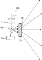
- FIG. 1 is a conceptual diagram of an example of an optical deflecting device of the present invention.
- FIG. 2 is a conceptual diagram of another example of the light deflection apparatus of the present invention.
- FIG. 3 is a conceptual diagram for explaining the operation of the optical deflection apparatus shown in FIG.
- FIG. 4 is a conceptual diagram of a liquid crystal optical phase modulation element.
- FIG. 5 is a conceptual diagram of a liquid crystal diffraction element.
- FIG. 6 is a schematic plan view of the optically anisotropic layer.
- FIG. 7 is a conceptual diagram for explaining the action of the optically anisotropic layer.
- FIG. 8 is a conceptual diagram for explaining the action of the optically anisotropic layer.
- FIG. 9 is a conceptual diagram for explaining the action of the optically anisotropic layer.
- FIG. 10 is a schematic plan view of another example of the optically anisotropic layer.
- FIG. 11 is a conceptual diagram of an exposure apparatus that exposes an alignment film.
- FIG. 12 is a conceptual diagram of another example of an exposure apparatus that exposes an alignment film.
- FIG. 13 is a conceptual diagram of another example of the light deflection apparatus of the present invention.
- FIG. 14 is a conceptual diagram of an optically anisotropic layer in an example of the present invention.
- FIG. 15 is a conceptual diagram of an optically anisotropic layer in an example of the present invention.
- FIG. 16 is a conceptual diagram for explaining the operation of an example of the optical deflecting device of the present invention.
- FIG. 17 is a diagram conceptually illustrating an example of the optical apparatus of the present invention.
- optical deflecting device of the present invention will be described below with reference to the drawings.
- the scale of the constituent elements is appropriately changed from the actual one for easy visual recognition.
- a numerical range expressed using “to” means a range including numerical values described before and after “to” as a lower limit value and an upper limit value.
- “orthogonal” and “parallel” with respect to the angle mean a range of a strict angle ⁇ 10 °.
- the optical deflecting device 100 of the present invention includes a condenser lens 131, a liquid crystal optical phase modulation element 101, a ⁇ / 4 plate 111, and an upstream side in the traveling direction of light (light beam).
- the liquid crystal optical phase modulation element 101 is an optical deflection element in the present invention, and is connected to a driving device 141.
- upstream and downstream are upstream and downstream in the light traveling direction.
- the ⁇ / 4 plate 111 and the liquid crystal diffraction element 121 are arranged on the emission side (downstream) of the liquid crystal optical phase modulation element 101, as shown in FIG. As shown in FIG. 1, the liquid crystal optical phase modulation element 101, the ⁇ / 4 plate 111, and the liquid crystal diffraction element 121 may be arranged in this section, or may be fixed using an adhesive or the like. Good.
- the liquid crystal optical phase modulation element 101, the ⁇ / 4 plate 111, and the liquid crystal diffraction element 121 are spaced so as not to deviate from the deflection angle of the light emitted from the liquid crystal optical phase modulation element 101.
- the same effect as that of the present invention can be obtained even if 102 is provided with a space.
- heat may be generated when passing, but by providing the interval 102, the heat generated by the light passing through the liquid crystal optical phase modulation element 101, the ⁇ / 4 plate 111, and ⁇ / 4
- the problem of melting the adhesive or the like that fixes the plate 111 and the liquid crystal diffraction element 121 can be avoided.
- the interval 102 is preferably 0.1 to 30 mm. In the case where the gap 102 is provided, the incident surface 103 of the liquid crystal diffraction element 121 is in contact with the air layer.
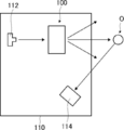
- FIG. 3 is a conceptual diagram for explaining the operation of the optical deflection apparatus 100 according to the embodiment of the present invention.
- the liquid crystal optical phase modulation element 101 deflects incident light 151 emitted from a light source (not shown) by a predetermined angle ⁇ ⁇ (see broken line).
- Incident light 151 is linearly polarized light in the direction indicated by arrow 171 in the figure.
- This linearly polarized light is P-polarized with respect to the exit surface 161 of the liquid crystal diffraction element 121 in the direction of polarization parallel to the cross-sectional view shown in FIG.
- S-polarized light may be used as the incident light 151. This can be dealt with by changing a part of the configuration of the liquid crystal optical phase modulation element 101.
- the maximum value of the variable range of the angle ⁇ in the liquid crystal optical phase modulation element 101 is defined as the maximum deflection angle ⁇ max, where the deflection angle ⁇ by the liquid crystal optical phase modulation element 101 is counterclockwise.
- the liquid crystal described later is set so that the emission angle when the light having the maximum deflection angle ⁇ max is incident on the liquid crystal diffraction element 121 becomes the target maximum emission angle ⁇ maxout in the optical deflecting device 10.
- the periodic structure pitch (rotation period p described later) in the optically anisotropic layer 14 of the diffraction element 121 is determined. In this way, even if the maximum deflection angle ⁇ max of the liquid crystal optical phase modulation element 101 is small, the maximum deflection angle ⁇ max by the liquid crystal optical phase modulation element 101 is set to the maximum target angle in the optical deflection apparatus 10 by the liquid crystal diffraction element 121. It becomes possible to expand to the emission angle ⁇ maxout. Similarly, when the angle ⁇ is in the negative direction, that is, clockwise, the maximum output angle of the light deflecting device 10 is the maximum output angle when the maximum deflection angle ⁇ max is the maximum value of the variable range of the angle ⁇ . By determining the periodic structure pitch so as to be the angle ⁇ maxout, the maximum deflection angle ⁇ max can be expanded to the target maximum emission angle ⁇ maxout even when the angle ⁇ is in the negative direction.
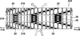
- the liquid crystal diffraction element 121 in order to increase the deflection angle of the emitted light, the liquid crystal diffraction element 121 gradually increases from the center of deflection (deflection azimuth) by the liquid crystal optical phase modulation element 101 toward the outside (both ends). Increase the diffraction angle.
- the periodic structure pitches (rotation periods p) of 121a, 121b, and 121c, which are regions of the liquid crystal diffraction element 121 are pa, pb, and pc
- the relationship of pa ⁇ pb ⁇ pc is established. Means there is.
- the periodic structure pitches of 121d and 121e are pd and pe, it means that there is a relationship of pe ⁇ pd ⁇ pc.
- the light is reduced by the liquid crystal diffraction element 121 when the angle ⁇ of the light emitted from the liquid crystal optical phase modulation element 101 is small.
- the periodic structure pitch is increased so as to be diffracted, and the period is such that the light is largely diffracted by the liquid crystal diffraction element 121 as the angle ⁇ of the light emitted from the liquid crystal optical phase modulation element 101 approaches the maximum deflection angle ⁇ max.
- the structure pitch is gradually reduced. In this way, the angle range of the outgoing light of the liquid crystal optical phase element is ⁇ ⁇ max, but when it exits from the liquid crystal diffraction element 121, it is expanded to ⁇ ⁇ maxout.
- the incident angle of light before entering the liquid crystal diffractive element 121 is ⁇ 1
- the refractive index of the incident side medium is n1
- the outgoing angle of light after exiting the liquid crystal diffractive element 121 is ⁇ 2
- the incident side of the medium on the outgoing side is Assuming that the refractive index is n2, the wavelength of light is ⁇ , the periodic structure pitch of the liquid crystal diffraction element is p, and the diffraction order is m, these values are related by the following equation (101).
- n1 ⁇ sin ⁇ 1 ⁇ n2 ⁇ sin ⁇ 2 m ⁇ ⁇ / p (101)
- the angle of light emitted from the liquid crystal diffraction element 121 can be changed by changing the periodic structure pitch p (rotation period p) of the liquid crystal diffraction element 121.
- the angle when finally emitted to the air can be up to an absolute value of about 80 °, so the angle ⁇ can be expanded to a very large angle.
- the periodic structure pitch of the liquid crystal diffraction element 121 that is, the rotation period p of the optically anisotropic layer 14, in the plane, light can be continuously emitted in an arbitrary direction.
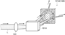
- the optical deflecting device 100 includes the condensing lens 131, the liquid crystal optical phase modulation element 101, the ⁇ / 4 plate 111, and the liquid crystal as the condensing element in the present invention from the upstream side in the light traveling direction. And a diffraction element 121.
- the condensing lens 131 is a known condensing lens, and condenses light incident on the liquid crystal light phase modulation element 101 slightly. In the light deflection apparatus 100 of the present invention, the condensing lens 131 is provided as a preferred embodiment.
- the light deflecting device 100 includes the condenser lens 131, so that the light (light beam) emitted from the light deflecting device 100 (liquid crystal diffraction element 121) can be converted into appropriate parallel light, thereby improving straightness. .
- the action of the condenser lens 131 will be described in detail later.
- the condensing element is not limited to the condensing lens 131, and all known optical elements capable of condensing light (light beam) can be used.
- FIG. 4 is a cross-sectional view showing an example of the structure of the liquid crystal optical phase modulation element in the embodiment of the present invention.
- the liquid crystal optical phase modulation element exemplified here the liquid crystal optical phase modulation element of Example 1 of JP-A-2003-295153 is cited.
- the liquid crystal optical phase modulation element is not limited to the illustrated example, and any known liquid crystal optical phase modulation element used as an optical deflection element can be used.
- FIG. 1 Light deflection element
- a nematic liquid crystal layer 501 shown as an example of a liquid crystal layer includes an alignment layer 209 formed to cover the composite electrode 211 of the first transparent substrate 201 of the liquid crystal optical phase modulation element 101, and a second transparent substrate 203.
- the alignment layer 209 formed so as to cover the common electrode 213 is homogeneously aligned so that the tilt angle ⁇ of the director 207 of p-type (positive-type) liquid crystal molecules when no electric field is applied is 5 ° or less.
- the incident light 151 that is linearly polarized light in the direction indicated by the arrow 171 is set to be linearly polarized light parallel to the light deflection direction by the liquid crystal optical phase modulation element 101.
- the incident light 151 becomes P-polarized light when viewed from the exit surface 161 of the liquid crystal diffraction element 121.
- the first transparent substrate 201 and the second transparent substrate 203 are fixed via a spacer (not shown) so that the nematic liquid crystal layer 501 maintains a predetermined constant thickness of several ⁇ m to several tens of ⁇ m.
- a spacer not shown
- tantalum pentoxide, silicon dioxide, or the like is provided on at least one of the composite electrode 211 and the common electrode 213.
- a transparent insulating film may be formed. It is also desirable to improve the transmittance by forming the transparent insulating film into a multilayer film composed of a high refractive index film and a low refractive index film.
- the common electrode 213 formed on the second transparent substrate 203 may be a full-surface electrode made of a transparent conductive film.
- the number of liquid crystal optical phase modulation elements 101 is one.
- the present invention is not limited to this, and a plurality of such liquid crystal optical phase modulation elements 101 are provided. You may do it.
- the alignment direction of the liquid crystal cell may be either parallel or vertical. When the alignment direction of the liquid crystal cell is parallel, it contributes to increasing the maximum deflection angle ⁇ max, and contributes to the enlargement of the deflection angle by the liquid crystal optical phase modulation element 101, that is, the deflection angle by the optical deflecting device 100.
- a driving device 141 is connected to the liquid crystal optical phase modulation element 101.
- the driving device 141 is a known driving device that drives the liquid crystal optical phase modulation element 101 and that corresponds to the configuration of the liquid crystal optical phase modulation element 101.
- the ⁇ / 4 plate 111 is a known ⁇ / 4 plate (1/4 phase difference plate) that converts the linearly polarized light deflected by the liquid crystal optical phase modulation element 101 into circularly polarized light.
- ⁇ / 4 plate 111 a known one can be used without limitation. Therefore, the ⁇ / 4 plate 111 may be derived from a polymer or liquid crystal.
- FIG. 5 conceptually shows the liquid crystal diffraction element 121.
- FIG. 5 is a view of the liquid crystal diffraction element 121 as viewed in the same direction as FIGS. 1 to 3, and is a side view of the liquid crystal diffraction element 121.
- the liquid crystal diffraction element 121 is a sheet-like element, and includes the support 12, the alignment film 13, and the optically anisotropic layer 14.
- the liquid crystal diffraction element 121 further diffracts the light deflected by the liquid crystal optical phase modulation element 101 in the deflection direction of the liquid crystal optical phase modulation element, thereby further deflecting the light deflected by the liquid crystal optical phase modulation element 101.
- the deflection angle of the maximum emission angle ⁇ maxout which is much larger than the maximum deflection angle ⁇ max of the liquid crystal optical phase modulation element 101. Enables deflection of light.
- the sheet surface direction of the liquid crystal diffraction element 121 is defined as the xy direction and the thickness direction is defined as the z direction.
- the horizontal direction in the figure is the direction in which the optical axis derived from the liquid crystal compound rotates in one direction (the axis A direction described later), and this direction is the x direction.
- the y direction is a direction orthogonal to the paper surface of FIG. 1 to 3, the vertical direction in the drawing corresponds to the x direction, the direction orthogonal to the paper surface corresponds to the y direction, and the horizontal direction in the drawing corresponds to the z direction.
- the x direction coincides with the deflection direction by the liquid crystal optical phase modulation element 101. This also applies to FIG. 13 described later.
- the liquid crystal diffraction element 121 is planar, but the liquid crystal diffraction element 121 is not limited to a planar shape, and may be a curved surface.
- the support 12 is preferably a transparent support, and examples thereof include polyacrylic resin films such as polymethyl methacrylate, cellulose resin films such as cellulose triacetate, and cycloolefin polymer films.
- examples of the cycloolefin polymer film include a product name “Arton” manufactured by JSR Corporation, a product name “Zeonor” manufactured by Nippon Zeon Corporation, and the like.
- the support 12 may be a flexible film or may be a non-flexible substrate such as a glass substrate.
- the alignment film 13 is formed on the surface of the support 12.
- the alignment film 13 is an alignment film for aligning the liquid crystal compound 20 in a predetermined liquid crystal alignment pattern when forming the optically anisotropic layer 14.
- the optically anisotropic layer 14 is a liquid crystal in which the orientation of the optical axis 22 derived from the liquid crystal compound 20 changes while continuously rotating along one direction in the plane. Has an alignment pattern. Therefore, the alignment film 13 of the liquid crystal diffraction element 121 is formed so that the optically anisotropic layer 14 can form this liquid crystal alignment pattern.
- the optically anisotropic layer 14 of the liquid crystal diffractive element 121 in one direction (direction along an axis A described later) in which the direction of the optical axis 22 in the liquid crystal alignment pattern changes while continuously rotating, The length that the direction rotates 180 ° is defined as one period (the rotation period p of the optical axis 22).
- the optically anisotropic layer 14 gradually shortens one period from the center of deflection (deflection azimuth (deflection direction)) by the liquid crystal optical phase modulation element 101 to the outside.
- the rotation direction of the optical axis of the liquid crystal compound 20 is reversed at the center of deflection by the liquid crystal optical phase modulation element 101 in the direction along the axis A (arrow x direction). Therefore, the alignment film 13 of the liquid crystal diffraction element 121 is formed so that the optically anisotropic layer 14 can form this liquid crystal alignment pattern.
- the alignment film 13 various known ones can be used.
- the alignment film 13 of the optically anisotropic layer 14 include a rubbing treatment film made of an organic compound such as a polymer, an oblique deposition film of an inorganic compound, a film having a microgroove, and ⁇ -tricosanoic acid, dioctadecylmethyl.
- examples thereof include films obtained by accumulating LB (Langmuir-Blodgett) films of organic compounds such as ammonium chloride and methyl stearylate by the Langmuir-Blodgett method.
- the alignment film 13 include those formed by rubbing the surface of the polymer layer.
- the rubbing treatment is performed by rubbing the surface of the polymer layer several times in a certain direction with paper or cloth.
- the types of polymers used for the alignment film are polyimide, polyvinyl alcohol, polymers having a polymerizable group described in JP-A-9-152509, JP-A-2005-97377, JP-A-2005-99228, and Further, an orthogonal alignment film described in JP-A-2005-128503 can be preferably used.
- the term “orthogonal alignment film” as used in the present invention means an alignment film that aligns the major axis of the molecules of the polymerizable rod-like liquid crystal compound of the present invention so as to be substantially orthogonal to the rubbing direction of the orthogonal alignment film.
- the thickness of the alignment film does not need to be large as long as it can provide an alignment function, and is preferably 0.01 to 5 ⁇ m, and more preferably 0.05 to 2 ⁇ m.
- a so-called photo-alignment film which is an alignment film by irradiating a photo-alignment material with polarized light or non-polarized light, can also be used. That is, a photo-alignment film may be produced by applying a light distribution material on the support 12. Irradiation with polarized light can be performed in a vertical direction or an oblique direction with respect to the photo-alignment film, and irradiation with non-polarized light can be performed in an oblique direction with respect to the photo-alignment film.
- Examples of the photo-alignment material used in the photo-alignment film that can be used in the present invention include, for example, JP-A-2006-285197, JP-A-2007-76839, JP-A-2007-138138, and JP-A-2007-94071.
- FIG. 11 shows a schematic diagram of an alignment film exposure apparatus that applies a photo-alignment material on the support 12 and dries it, and then exposes the alignment film to form an alignment pattern.
- the exposure apparatus 50 includes a light source 54 including a laser 52, a beam splitter 56 that separates the laser light 70 from the laser 52 into two, and mirrors disposed on the optical paths of the two separated light beams 72A and 72B. 58A, 58B and ⁇ / 4 plates 60A, 60B.
- the light source 64 includes, for example, a polarizing plate and emits linearly polarized light P 0 .
- lambda / 4 plate 60A and 60B is provided with an optical axes perpendicular to one another, lambda / 4 plate 60A is linearly polarized light P 0 on the right circularly polarized light P R, lambda / 4 plate 60B is left circularly linearly polarized light P 0 converting the polarization P L.
- the support 12 having the alignment film 13 before the alignment pattern is formed is disposed in the exposure portion, and the two light beams 72A and 72B are crossed on the alignment film 13 to interfere with each other. Irradiate and expose. Due to the interference at this time, the polarization state of the light applied to the alignment film 13 periodically changes in the form of interference fringes. Thereby, an alignment pattern in which the alignment state changes periodically can be obtained.
- the period of the alignment pattern can be changed by changing the crossing angle ⁇ of the two light beams 72A and 72B. That is, in the exposure apparatus 50, in the alignment pattern in which the optical axis 22 derived from the liquid crystal compound 20 continuously rotates along one direction by adjusting the crossing angle ⁇ , the optical axis 22 rotates in one direction.
- the length of one period (rotation period p) by which the optical axis 22 rotates 180 ° can be adjusted.
- an optically anisotropic layer 14 to be described later on the alignment film 13 having an alignment pattern in which the alignment state is periodically changed in this way, an optical anisotropy having a liquid crystal alignment pattern corresponding to this period is formed.
- Layer 14 can be formed.
- the rotation direction of the optical shaft 22 can be reversed by rotating the optical axes of the ⁇ / 4 plate 60A and the ⁇ / 4 plate 60B by 90 °. Accordingly, masking is performed on the half surface of the alignment film 13 to perform exposure, then masking is performed on the exposed area, and the optical axes of the ⁇ / 4 plate 60A and the ⁇ / 4 plate 60B are rotated by 90 °, respectively.
- the rotation direction of the optical axis 22 can be reversed at the center.
- the length of one cycle in which the optical axis 22 rotates 180 ° (rotation cycle p) ) Can be gradually shortened from the center of one direction in which the optical axis 22 rotates toward the outside.
- An exposure apparatus 80 conceptually shown in FIG. 12 is also preferably used for exposing the alignment film 13.
- An exposure apparatus 80 shown in FIG. 12 is an exposure apparatus that is also used when forming a concentric liquid crystal alignment pattern as shown in FIG.
- the exposure apparatus 80 includes a light source 84 including a laser 82, a polarization beam splitter 86 that divides the laser light M from the laser 82 into S-polarized MS and P-polarized MP, and a mirror 90A disposed in the optical path of the P-polarized MP.
- a mirror 90B disposed in the optical path of S-polarized MS, a lens 92 (convex lens) disposed in the optical path of S-polarized MS, a polarization beam splitter 94, and a ⁇ / 4 plate 96.
- the P-polarized light MP divided by the polarization beam splitter 86 is reflected by the mirror 90A and enters the polarization beam splitter 94.
- the S-polarized light MS divided by the polarization beam splitter 86 is reflected by the mirror 90B, collected by the lens 92, and incident on the polarization beam splitter 94.
- the P-polarized light MP and the S-polarized light MS are combined by the polarization beam splitter 94 to become right circularly polarized light and left circularly polarized light according to the polarization direction by the ⁇ / 4 plate 96, and the alignment film 13 on the support 12. Is incident on.
- the polarization state of the light applied to the alignment film 13 periodically changes in the form of interference fringes.
- the crossing angle of the left circularly polarized light and the right circularly polarized light changes, so that an exposure pattern whose pitch changes from the inside to the outside can be obtained.
- the alignment film 13 a concentric alignment pattern in which the alignment state changes periodically is obtained.
- the length of one period (rotation period p) in which the optical axis 22 of the liquid crystal compound 20 continuously rotates 180 ° along one direction is the refractive power of the lens 92 (F number of the lens 92). It can be controlled by changing the focal length of the lens 92, the distance between the lens 92 and the alignment film 13, and the like. Further, by adjusting the refractive power of the lens 92 (F-number of the lens 92), the length of one cycle in which the optical shaft 22 rotates 180 ° can be changed in one direction in which the optical shaft 22 rotates continuously.
- the length of one cycle in which the optical axis 22 rotates by 180 ° can be changed according to the degree of condensing of the light transmitted through the lens 92 that interferes with the parallel light. More specifically, when the refractive power of the lens 92 is weakened, it approaches parallel light, so that the length of one cycle in which the optical axis 22 rotates 180 ° gradually decreases from the inside toward the outside, and the F number is growing. On the contrary, when the refractive power of the lens 92 is increased, the length of one period in which the optical axis 22 rotates 180 ° is suddenly shortened from the inside toward the outside, and the F number is reduced.
- a configuration in which the optical axis 22 of the liquid crystal compound 20 continuously rotates and changes only in the direction can also be used.
- an optical element that transmits light so as to be condensed can be obtained.
- an optical element that transmits light so as to diffuse only in the arrow X direction can be obtained.
- An optical element that transmits light so as to diffuse only in the X direction of the arrow can also be obtained by reversing the turning direction of the incident circularly polarized light. Further, depending on the use of the optical element, for example, when it is desired to provide a light amount distribution in the transmitted light, one cycle in which the optical axis 22 rotates 180 degrees toward the arrow X direction is not gradually changed, but in the arrow X direction. Also, a configuration in which the optical axis 22 is partially rotated by 180 ° and has a region with different one cycle can be used.
- a method of scanning and patterning the photo-alignment film while arbitrarily changing the polarization direction of the condensed laser light is used. be able to.
- the alignment film 13 is provided as a preferred embodiment and is not an essential component.
- the optically anisotropic layer 14 is derived from the liquid crystal compound 20 by forming an alignment pattern on the support 12 by a method of rubbing the support 12, a method of processing the support 12 with a laser beam, or the like. It is also possible to adopt a configuration having a liquid crystal alignment pattern in which the orientation of the optical axis 22 is changed while continuously rotating along at least one in-plane direction.
- an optically anisotropic layer 14 that is a cured layer of a liquid crystal composition containing the liquid crystal compound 20 is provided on the surface of the alignment film 13.
- the optical axis (slow axis) of the liquid crystal compound is a liquid crystal pattern arranged along at least one direction in the plane of the optically anisotropic layer, and the optical axis of the liquid crystal compound 20.
- the direction of the axis 22 has a liquid crystal alignment pattern that is rotationally changed in one direction.
- the retardation R is preferably 0.4 ⁇ to 0.6 ⁇ , more preferably 0.45 ⁇ to 0.55 ⁇ , and particularly preferably 0.5 ⁇ .
- ⁇ n is the birefringence of the optically anisotropic layer 14
- d 1 is the thickness.
- the retardation R for light of 940 nm may be in the range of 338 to 602 nm, and is particularly preferably 470 nm.
- the liquid crystal diffraction element 121 functions as a transmission type diffraction grating.
- the principle of functioning as a diffraction grating will be described with reference to FIGS. 6 is a schematic plan view of the optically anisotropic layer 14, that is, FIG. 5 is a view of the optically anisotropic layer 14 as viewed from above.
- the liquid crystal compound 20 is fixed in a liquid crystal alignment pattern in which the optical axis 22 is continuously rotated in one direction.
- the optical axis 22 continuously rotates and changes in the direction along the axis A in FIG.
- the liquid crystal compound 20 is aligned so that the angle formed by the axis A and the in-plane component of the major axis (abnormal light axis: director) of the liquid crystal compound 20 defined as the optical axis 22 changes. .
- the direction of the optical axis 22 of the liquid crystal compound 20 is the same in the liquid crystal compound 20 aligned in the direction orthogonal to the axis A, that is, in the arrow y direction. Yes.
- the optically anisotropic layer 14 exhibits a function as a general ⁇ / 2 plate as described above for each region in which the direction of the optical axis 22 of the liquid crystal compound 20 in the y direction coincides.
- the angle formed between the optical axis 22 and the axis A of the liquid crystal compound 20 arranged along the axis A differs from the liquid crystal alignment pattern in which the direction of the optical axis 22 is rotated and changed depending on the position in the axis A direction.
- the pattern is oriented and fixed so that the angle formed by the optical axis 22 and the axis A along the axis A gradually changes from ⁇ to ⁇ + 180 ° or ⁇ 180 °.
- the optical axis 22 of the liquid crystal compound 20 is parallel to the surface of the optically anisotropic layer 14, and the direction of the optical axis 22 is constant.
- a local region that is, a region in which the liquid crystal compound 20 is arranged in the arrow y direction is arranged in the x direction orthogonal to the arrow y direction, and between the plurality of local regions arranged in the arrow x direction.
- the liquid crystal alignment pattern in which the orientation of the optical axis 22 is continuously rotated in one direction (the direction along the axis A) is referred to as horizontal rotational alignment.
- the change in the angle of the optical axis 22 in the direction of the axis A may be an object that rotates at nonuniform angular intervals instead of a constant angular interval.
- the average value of the direction of the optical axis 22 in the unit region is linearly changed at a constant rate, it is gradually changed.
- the change in the inclination of the optical axis between the unit regions adjacent to each other in the direction of the axis A and having different inclinations of the optical axis 22 is 45 ° or less.
- the change in the inclination of the adjacent unit region is preferably smaller.
- the rotation period p is preferably 0.5 to 5 ⁇ m. The shorter the rotation period p, the larger the diffraction angle by the optically anisotropic layer 14, that is, the liquid crystal diffraction element 121. Therefore, the rotation period p may be determined according to the wavelength of the incident light to the liquid crystal diffraction element 121 and a desired emission angle.
- the liquid crystal diffraction element 121 gives a phase difference of ⁇ / 2 to the incident light, and enters the incident light at an incident angle of 0 °, that is, vertically incident light. emit at theta 2. That is, as shown in FIG. 7 to be described later, when light is incident L 1 side in vertical right circular polarization P R of the optically anisotropic layer 14, left circular polarization in the direction forming an normal direction and the angle theta 2 P L light L 2 is emitted.
- that light is incident on the surface of the optically anisotropic layer 14 perpendicularly means that light is incident along the normal of the surface.
- the light L 1 of the right circularly polarized light P R incident on the optical anisotropic layer 14 is also referred to as “incident light L 1 ”.
- the light L 2 of the left circularly polarized light P L emitted from the optically anisotropic layer is also referred to as “emitted light L 2 ”.
- Liquid crystal diffraction element 121 case of incident light of a predetermined wavelength, as the rotation period p in the optically anisotropic layer 14 is small, the emission angle of the diffraction angle or the outgoing light L 2 is increased.
- the exit angle of the outgoing light L 2 is the angle formed by the normal direction of the optically anisotropic layer 14 and the outgoing light L 2 is.
- the diffraction direction of the outgoing light L 2 from the liquid crystal diffraction element 121 is the circular polarization of the light incident on the liquid crystal diffraction element 121.
- the incident is controlled. That is, when the incident light is linearly polarized light as shown in the example, the ⁇ / 4 plate 111 is inserted and converted to either the left or right circularly polarized light, so that the incident direction of light diffraction can be changed. Can only be.
- FIG. 7 is a diagram schematically showing the principle that incident light L 1 perpendicularly incident on the optically anisotropic layer 14 is emitted at a predetermined emission angle ⁇ 2 .
- incident light L 1 perpendicularly incident on the optically anisotropic layer 14 is emitted at a predetermined emission angle ⁇ 2 .
- the incident light L 1 is a right circularly polarized light P R, by passing through the optically anisotropic layer 14, a phase difference of lambda / 2 is converted given to left-handed circularly polarized light P L.
- the incident light L 1 is the optical axis 22 of the liquid crystal compound 20 in each unit region in a plane (local area), the absolute phase changes.
- the orientation of the optical axis 22 of the liquid crystal compound 20 changes by rotating toward the axis A direction (in this example, the direction of the arrow x), so that the incident light
- the amount of change in the absolute phase varies depending on the direction of the optical axis 22 of the liquid crystal compound 20 at the x coordinate (the position in the x direction) of the surface (xy plane) of the optically anisotropic layer 14 on which is incident.
- a region indicated by a broken line in FIG. 7 schematically shows that the change amount of the absolute phase varies depending on the x coordinate. As shown in FIG.
- an absolute phase equiphase surface 24 having an angle with respect to the surface of the optically anisotropic layer is formed by the deviation of the absolute phase when passing through the optically anisotropic layer 14.
- the incident light L 1 incident from the normal direction the bending force is applied in a direction perpendicular to the equiphase plane 24, the traveling direction of the incident light L 1 is changed. That is, the incident light L 1 is a right circularly polarized light P R, the after passing through the optically anisotropic layer 14 left-handed circularly polarized light P L becomes and proceeds to a direction forming a normal direction at a predetermined angle theta 2 It is emitted from the optically anisotropic layer 14 as an outgoing light L 2.
- the liquid crystal in the diffraction element 121 As described above, the liquid crystal in the diffraction element 121, the incident light L 1 incident along the normal direction perpendicular to the plane of the liquid crystal diffraction element 121, output light L 2 in a direction different from the normal direction Is emitted.
- the inclination of the emission angle can be changed by changing the rotation period p in the direction of the optical axis in the liquid crystal alignment pattern in the optical anisotropic layer 14. As the rotation period P is decreased, a larger bending force can be applied to the incident light, so that the inclination can be increased.
- the wavefront of the incident light can be changed by changing the amount of change in absolute phase by the liquid crystal alignment pattern in the optically anisotropic layer 14.
- the conversion of the incident light L 1 to the outgoing light L 2 based on the above principle is transmission diffraction.
- Optically anisotropic layer 14 with respect to the incident light L 1 acts as a transmission grating, the incident light L 1 which is perpendicularly incident on the optically anisotropic layer 14, predetermined diffraction angle theta 2 of the emitted light (transmitted diffraction light) It is transmitted diffracted as L 2.
- equation (1) which is a general light diffraction equation, is satisfied.
- n 1 is the refractive index of the medium 1 on the incident surface side of the diffraction grating (here, the optically anisotropic layer 14), ⁇ 1 is the incident angle, and n 2 is the diffraction grating (here, the optically anisotropic layer).
- the refractive index of the medium 2 on the exit surface side, ⁇ 2 is the diffraction angle (exit angle), ⁇ is the wavelength, p is the rotation period, and m is the order of diffraction.
- FIG. 8 is a diagram schematically illustrating the diffraction phenomenon represented by the equation (2).
- An optically anisotropic layer 14 as a diffraction grating is disposed between the medium n 1 and the medium n 2 .
- Light L 1 incident on the optically anisotropic layer 14 from the normal direction from the medium 1 side is a refractive index n 1 is diffracted by the diffraction effect of the optically anisotropic layer 14, the refractive index n 2 medium 2 Emitted to the side.
- the emitted light L 2 emitted by the emission angle theta 2 time can be rephrased as transmitted diffraction light L 2 of the diffraction angle theta 2.
- the optically anisotropic layer 14 in which the liquid crystal compound 20 is horizontally rotated and fixed functions as a diffraction grating.
- the wavelength ⁇ of the light that causes the diffraction action by the liquid crystal diffraction element 121 may be from ultraviolet to visible light, infrared, or even an electromagnetic wave level.
- the diffraction angle increases as the wavelength of incident light increases, and the diffraction angle decreases as the wavelength of incident light decreases.
- the liquid crystal compound 20 a rod-like liquid crystal compound and a disk-like liquid crystal compound can be used.
- the wavelength ⁇ is 380 nm
- the disc-shaped liquid crystal compound can obtain higher diffraction efficiency than the rod-shaped liquid crystal compound when the rotation period p ( ⁇ m) is in the range of 0.5 ⁇ p ⁇ 1.
- the wavelength ⁇ is 1100 nm
- the discotic liquid crystal compound can obtain higher diffraction efficiency than the rod-shaped liquid crystal compound when the rotation period p ( ⁇ m) is in the range of 2 ⁇ p ⁇ 5.
- the liquid crystal diffraction element 121 (optically anisotropic layer 14), if the light is incident L 41 of randomly polarized light, among the incident light L 41, right circularly polarized light P R As described above, this component is converted into left circularly polarized light P L in the optically anisotropic layer 14, undergoes a bending force due to the liquid crystal alignment pattern, changes its traveling direction, passes through the optically anisotropic layer, It is emitted as transmitted diffraction light L 42 1.
- components of the left circularly polarized light P L of the incident light L 41 together are converted into right circularly polarized light P R in the optically anisotropic layer 14 was converted from right circularly polarized light into left-handed circularly polarized light
- the light travels through the optical anisotropic layer 14 in a changed state, and is emitted as the second transmitted diffracted light L 43 from the opposite surface of the liquid crystal diffraction element 121.
- the traveling directions of the first transmitted diffracted light L 42 and the second transmitted diffracted light L 43 are substantially axisymmetric with respect to the normal line.
- the rotation period may be designed so as to obtain a desired diffraction angle ⁇ 2 so as to satisfy the above formula (1) in consideration of the incident angle ⁇ 1 .
- the optical deflecting device 100 of the present invention refracts (diffracts) the light deflected by the liquid crystal optical phase modulation element 101 by the liquid crystal diffraction element 121 (optical anisotropic layer 14), so that the liquid crystal optical phase.
- the light can be deflected by the deflection angle of the maximum emission angle ⁇ maxout which is much larger than the maximum deflection angle ⁇ max of the modulation element 101.
- the refraction (diffraction angle) of light by the optically anisotropic layer 14 increases as one period in which the optical axis 22 of the liquid crystal compound 20 rotates 180 °, that is, the rotation period p is shorter.
- the polarization direction (swing direction) of the incident circularly polarized light is the same, the light refraction direction by the optical anisotropic layer 14 is reversed depending on the rotation direction of the optical axis 22 of the liquid crystal compound 20. That is, when the incident light L 1 is a right circularly polarized light P R, as viewed from the exit surface side, the rotational direction of the optical axis 22, in the axial direction A (direction of arrow x) as shown in FIGS. 5 to 7 When it is clockwise, the outgoing light L2 is refracted in the direction of the axis A, for example.
- the optical anisotropic layer 14 deflects the rotation period p of the optical axis 22 of the liquid crystal compound 20 in the direction of the axis A by the liquid crystal optical phase modulation element 101 (
- the deflection direction is gradually shortened from the center to the outside. That is, the amount of light refracted by the optically anisotropic layer 14 increases toward the outside in the deflection direction.
- the optical anisotropic layer 14 has the rotational direction of the optical axis 22 of the liquid crystal compound 20 directed in the direction of the axis A at the center of deflection by the liquid crystal optical phase modulation element 101. Reverse.
- the optical deflection apparatus 100 of the present invention enables light deflection by the deflection angle of the maximum emission angle ⁇ maxout that is much larger than the maximum deflection angle ⁇ max of the liquid crystal optical phase modulation element 101. ing.
- the direction of rotation of the optical axis 22 is usually reversed at the center of the optical anisotropic layer 14 in the direction of the axis A (arrow x direction), that is, the direction in which the optical axis 22 rotates. That is, in the optical deflecting device 100, the center of deflection in the liquid crystal optical phase modulation element 101 and the center in the axis A direction in the optical anisotropic layer 14 are usually matched.
- the rotation period p may be continuously shortened from the center of deflection toward the outside, or may be shortened stepwise.
- the optically anisotropic layer 14 is formed of a liquid crystal composition containing a liquid crystal compound.
- the liquid crystal composition containing a liquid crystal compound for forming the optically anisotropic layer 14 contains other components such as a leveling agent, an alignment controller, a polymerization initiator and an alignment aid in addition to the liquid crystal compound. May be.
- An optically anisotropic layer in which a predetermined liquid crystal alignment pattern is fixed, comprising a cured layer of a liquid crystal composition by forming an alignment film on a support and applying and curing the liquid crystal composition on the alignment film Can be obtained.
- each component of the liquid crystal composition of the present invention will be described in detail.
- the optically anisotropic layer 14 is a cured layer of a liquid crystal composition containing a rod-like liquid crystal compound or a discotic liquid crystal compound, and the optical axis of the rod-like liquid crystal compound or the optical axis of the discotic liquid crystal compound is aligned as described above. It has a liquid crystal alignment pattern.
- an optically anisotropic layer composed of a cured layer of the liquid crystal composition can be obtained.
- the optically anisotropic layer functions as a so-called ⁇ / 2 plate
- the present invention includes a mode in which a laminated body integrally including the support 12 and the alignment film functions as a ⁇ / 2 plate. .
- the liquid crystal composition for forming the optically anisotropic layer contains a rod-like liquid crystal compound or a disk-like liquid crystal compound, and other components such as a leveling agent, an alignment controller, a polymerization initiator, and an alignment aid. May be contained.
- the optically anisotropic layer preferably has a wide band with respect to the wavelength of incident light, and is preferably formed using a liquid crystal material having a birefringence index that is inversely dispersed. Furthermore, it is also preferable to make the optically anisotropic layer substantially broadband with respect to the wavelength of incident light by imparting a twisting component to the liquid crystal composition and by laminating different retardation layers.
- Japanese Unexamined Patent Application Publication No. 2014-089476 discloses a method for realizing a broadband ⁇ / 2 plate by laminating two liquid crystal layers having different twist directions in an optically anisotropic layer. Can be preferably used in the present invention.
- rod-like liquid crystal compounds examples include azomethines, azoxys, cyanobiphenyls, cyanophenyl esters, benzoic acid esters, cyclohexanecarboxylic acid phenyl esters, cyanophenylcyclohexanes, cyano-substituted phenylpyrimidines, alkoxy-substituted phenylpyrimidines, Phenyldioxanes, tolanes, and alkenylcyclohexylbenzonitriles are preferably used.
- high-molecular liquid crystalline molecules can also be used.
- the polymerizable rod-like liquid crystal compound examples include those described in Makromol. Chem. 190, 2255 (1989), Advanced Materials, 5, 107 (1993), US Pat. No. 4,683,327, US Pat. No. 5,622,648, US Pat. No. 5,770,107, International Publication No. 95/22586, 95/24455, 97/00600, 98/23580, 98/52905, JP-A-1-272551, 6-16616, 7-110469, 11-80081 And the compounds described in Japanese Patent Application No. 2001-64627 and the like can be used. Further, as the rod-like liquid crystal compound, for example, those described in JP-A-11-513019 and JP-A-2007-279688 can be preferably used.
- the discotic liquid crystal compound for example, those described in JP-A-2007-108732 and JP-A-2010-244038 can be preferably used.
- the liquid crystal compound 20 rises in the thickness direction in the optically anisotropic layer, and the optical axis 22 derived from the liquid crystal compound has a disc surface. It is defined as an axis perpendicular to the so-called fast axis.
- the optically anisotropic layer 14 can be formed by applying a multilayer liquid crystal composition on the alignment film 13.
- a liquid crystal composition is applied on an alignment film, heated, cooled, and then cured with ultraviolet rays to produce a first liquid crystal immobilization layer. It refers to repeating coating by coating on the chemical layer, heating in the same manner, and performing UV curing after cooling.
- the light deflection apparatus 100 in the illustrated example includes the condenser lens 131 on the upstream side of the liquid crystal optical phase modulation element 101 as a preferable aspect.
- the refraction of light by the optically anisotropic layer 14 gradually increases from the center in the deflection direction to the outside.
- the light deflected by the optical deflecting device 100 that is, the light beam actually has a thickness.
- the amount of light refracted by the optically anisotropic layer 14 is strictly different between the inside (the center of deflection) and the outside in the deflection direction, and the outside is larger in the amount of refraction.
- the light refracted by the liquid crystal diffraction element 121 becomes light that expands slightly so as to diffuse.
- the condenser lens 131 is provided, and the light incident on the liquid crystal diffractive element 121 is made to have a slightly reduced diameter, so that the light emitted from the light deflecting device 100 (liquid crystal diffractive element 121) is parallel. It is possible to improve straightness by using light. As a result, by providing the condensing lens 131, the light scanning by the light deflecting device 100 can be accurately performed even if the object to be scanned by the light is far from the light deflecting device 100.
- the refractive power (lens power) of the condenser lens 131 is not limited. That is, the refractive power of the condensing lens 131 includes the amount of light refracted by the liquid crystal diffraction element 121 and its in-plane distribution (that is, the in-plane distribution function of the diffraction pitch), the light deflection angle by the light deflecting device 100, and the light deflecting device.
- the refractive power capable of emitting suitable light may be set as appropriate according to the distance between 100 and the optical scanning target, the light diameter (beam diameter) of incident light, and the like.
- the position of the condenser lens 131 may be upstream from the liquid crystal diffraction element 121. However, the liquid crystal optical phase can be reduced in that the condenser lens 131 can be downsized and the condenser lens 131 can be easily designed. It is preferable to be upstream of the modulation element 101 (light deflection element).
- FIG. 10 is a schematic plan view of an optically anisotropic layer in a design change example of the liquid crystal diffraction element.
- the liquid crystal alignment pattern in the optically anisotropic layer 14A shown in FIG. 10 is different from the liquid crystal alignment pattern in the optically anisotropic layer 14 described above. In FIG. 10, only the optical axis 22 is shown.
- the optically anisotropic layer 14A in FIG. 10 is a liquid crystal in which the orientation of the optical axis 22 is changed by gradually rotating along multiple directions from the center side to the outer side, for example, the axes A 1 , A 2 , A 3 . It has an orientation pattern. That is, the liquid crystal alignment pattern of the optically anisotropic layer 14A shown in FIG.
- the liquid crystal alignment pattern of the optically anisotropic layer 14A shown in FIG. 10 is a concentric pattern having one direction in which the direction of the optical axis changes while continuously rotating, concentrically from the inside toward the outside. It is.
- the absolute phase of incident light changes with different amounts of change between local regions in which the direction of the optical axis 22 is different. If a liquid crystal alignment pattern whose optical axis rotates in a radial manner as shown in FIG. 10 is provided, the incident light can be transmitted as diverging light or condensed light. That is, the function as a concave lens or a convex lens can be realized by the liquid crystal alignment pattern in the optical anisotropic layer 14.
- the center of the lens when aligned with the center of the light emitted from the liquid crystal light phase modulation element 101, the light can be spread most efficiently at the maximum deflection angle ⁇ max emitted from the liquid crystal light phase modulation element.
- the light deflecting device of the present invention can deflect light so as to diffuse radially from the center by using the function of the concave lens of the optically anisotropic layer 14A shown in FIG. 10 for the liquid crystal diffraction element 121A.
- a deflection element 101A is used.
- the light deflection element 101A deflects light at an azimuth of 360 ° and a polar angle of 0 to 35 °.
- the light L deflected radially by the light deflecting element 101A is refracted by the liquid crystal diffractive element 121A, so that the deflection angle, that is, the azimuth angle by the light deflecting element 101A is expanded, and a wide range is obtained.
- the light can be deflected radially.
- a condensing lens 131 is provided as a preferred embodiment.
- the condenser lens 131 By the condenser lens 131, the light L is incident on the light deflecting element 101A as the condensed light, deflected, and directly incident on the liquid crystal diffractive element 121A as the condensed light, so that the light refracted by the liquid crystal diffractive element 121A is collimated. It can be deflected and emitted as light.
- a MEMS (Micro Electro Mechanical Systems) optical deflecting element described in Japanese Patent Laid-Open No. 2012-208352 is disclosed as an example.
- a mirror By oscillating a mirror (mirror) using a piezoelectric actuator or the like, such as a MEMS optical deflecting element described in 134642 and a MEMS optical deflecting element described in JP-A-2015-22064, light is emitted.
- MEMS optical deflection elements MEMS (optical) scanners, MEMS optical deflectors, MEMS mirrors, DMDs (Digital Micromirror Devices)) that perform deflection (deflection scanning).
- the liquid crystal compound 20 of the liquid crystal diffraction element is oriented in one direction in the thickness direction, but the present invention is not limited to this.
- the optical anisotropic layers constituting the liquid crystal diffraction element are the same as the first optical anisotropic layer 215 and the second optical anisotropic layer 216 of the liquid crystal diffraction element 220 shown in FIG.
- the liquid crystal compound 20 may be twisted and aligned along a helical axis extending along the thickness direction. In the following description, the twist orientation along the helical axis extending along the thickness direction is also simply referred to as “twist orientation”.
- the first optical anisotropic layer 215 and the second optical anisotropic layer 216 in which the liquid crystal compound 20 is twisted and aligned are cross sections obtained by observing the cross section of the liquid crystal diffraction element 220 with a scanning electron microscope (SEM).
- SEM scanning electron microscope
- the optical axis of the liquid crystal compound when the optical axis of the liquid crystal compound is gradually shortened in the direction in which the optical axis 22 rotates by one period (rotation period p) that rotates 180 degrees,
- the inclination angle of the bright and dark lines with respect to the normal line of the first optical anisotropic layer 215 and the second optical anisotropic layer 216 gradually decreases in the direction in which the optical axis 22 rotates. That is, in this case, the inclination angle of the bright and dark lines rises with respect to the main surface of the optically anisotropic layer.
- the bright and dark line patterns of the first optical anisotropic layer 215 and the second optical anisotropic layer 216 have a shorter period in the direction in which the optical axis 22 rotates.
- the diffraction efficiency of light can be improved even with high-angle diffraction.
- the light amount in the optically anisotropic layer can be suppressed and the amount of emitted light can be improved.
- the first optical anisotropic layer 215 and the second optical anisotropic layer 216 have different twist directions in the twist alignment of the liquid crystal compound 20. That is, in the first optical anisotropic layer 215, the liquid crystal compound 20 is twisted and oriented clockwise in the light traveling direction. On the other hand, in the second optical anisotropic layer 216, the liquid crystal compound 20 is twisted and oriented counterclockwise in the light traveling direction. Therefore, the first optically anisotropic layer 215 and the second optically anisotropic layer 216 have different inclination directions of bright and dark lines derived from the twisted orientation in the cross-sectional SEM image.
- first optically anisotropic layer 215 for example, when the incident light is right circularly polarized light, the diffraction efficiency is improved for light traveling toward the left side (outside) in the figure indicated by the solid line. Great effect is obtained.
- the first optically anisotropic layer 215 improves the diffraction efficiency for light traveling toward the right side (center side) in the drawing indicated by the broken line, for example, when the incident light is right circularly polarized light. The effect is small.
- the second optical anisotropic layer 216 when the incident light is right circularly polarized light, on the contrary, the diffraction efficiency is improved with respect to the light traveling toward the left side (outside) in the figure indicated by the solid line.
- the effect is small.
- the second optically anisotropic layer 216 has a great effect of improving the diffraction efficiency with respect to light traveling toward the right side (center side) in the drawing indicated by the broken line. This effect is reversed when the incident light is left circularly polarized light.
- the liquid crystal diffraction element 220 In the liquid crystal diffraction element 220, only light traveling toward the left side (outer side) in the figure indicated by the solid line enters the region shown in FIG. 14 where the center of deflection is on the right side in the figure. Therefore, in this light (right circularly polarized light), that is, in the region on the left side in the figure from the center, the first optical anisotropic layer 215 acts strongly, improving the diffraction efficiency and increasing the amount of emitted light. . On the other hand, in the region on the right side of the center with respect to the region shown in FIG. 14, only the light traveling toward the right side in the drawing indicated by the broken line is incident.
- the second optical anisotropic layer 216 acts strongly on this light (right circularly polarized light), improving the diffraction efficiency and increasing the amount of emitted light. Further, since the incident angle of incident light with respect to the optical anisotropic layer is small in the central region of the polarized light, both the first optical anisotropic layer 215 and the second optical anisotropic layer 216 improve the diffraction efficiency. Contribute. As a result, according to the liquid crystal diffraction element 220 having the first optical anisotropic layer 215 and the second optical anisotropic layer 216 in which the twist directions in the twist alignment of the liquid crystal compound 20 are different from each other, the entire region in the light deflection direction. The effect of improving the diffraction efficiency can be obtained, and a large amount of light can be emitted over the entire deflection angle.
- the twist angle of the liquid crystal compound is not limited. What is necessary is just to set suitably the twist angle of a liquid crystal compound according to the deflection angle by an optical deflection element, the target diffraction efficiency, etc.
- the twist angle of the liquid crystal compound 20 is preferably 10 to 200 °, more preferably 20 to 190 °, and still more preferably 40 to 170 °.
- the twist angle (twist angle in the thickness direction) of the liquid crystal compound 20 that is twist-oriented is the twist angle of the liquid crystal compound 20 that is twist-aligned along the helical axis extending in the thickness direction in the optically anisotropic layer. This is the twist angle from the lower surface to the upper surface.
- the liquid crystal diffraction element having the first optical anisotropic layer 215 and the second optical anisotropic layer 216 in which the liquid crystal compound 20 is twisted and twisted in a spiral shape is like a liquid crystal diffraction element 224 shown in FIG.
- the liquid crystal compound 20 may have a third optical anisotropic layer 219 in which the twisted orientation is not performed.
- the third optical anisotropic layer 219 in which the liquid crystal compound is not twisted and aligned is a non-tilted optical anisotropic layer in which bright and dark lines extend along the normal direction.
- liquid crystal diffraction element 121 has been described as a transmission type diffraction element, a reflection type liquid crystal diffraction element can also be used in the optical deflection apparatus of the present invention. In that case, the same formation method can be adopted only by changing the liquid crystal composition.
- a cholesteric liquid crystal as the liquid crystal and using an alignment film similar to the transmission type, reflection type diffracted light can be generated and used for angle expansion.
- a light reflecting element that reflects light in a direction different from the incident angle, it can be applied as a condensing mirror for a sensor as a micromirror that collects or diverges light, or as a microlens.
- the optical deflection element is not limited to the liquid crystal optical phase modulation element 101, and various known optical deflection elements such as a galvano mirror, a polygon mirror, and a MEMS optical deflection element can be used. It is. Among them, the liquid crystal optical phase modulation element 101 and the MEMS optical deflection element described above are preferably used as the optical deflection element in that the mechanical movable part is small and the mechanical movable part is small.
- FIG. 13 conceptually shows an example of the optical deflection apparatus of the present invention using a MEMS optical deflection element.
- the optical deflector 130 shown in FIG. 13 uses many of the same members as those of the optical deflector 100 described above. Therefore, the same reference numerals are given to the same members, and the following description mainly focuses on different parts.
- the P-polarized light emitted from the light source (not shown) is slightly condensed by the condenser lens 131 with respect to the emission surface 161 of the liquid crystal diffraction element 121, and then ⁇ For example, it is converted into right circularly polarized light by the / 4 plate 111.
- the ⁇ / 4 plate 111 is disposed between the MEMS optical deflection element 132 and the liquid crystal diffraction element 121, as in the optical deflection apparatus 100 shown in FIG. Also good.
- the ⁇ / 4 plate 111 is preferably provided upstream of the MEMS optical deflecting element 132 in the optical deflecting device 130 using the MEMS optical deflecting element 132 in that the ⁇ / 4 plate 111 can be reduced in size. . Further, in the optical deflection device 130 using the MEMS optical deflection element 132, the ⁇ / 4 plate 111 may not be provided when circularly polarized light is incident.
- the mirror of the MEMS optical deflection element 132 is preferably one that does not depolarize. Specifically, it is a metal mirror or the like showing a mirror surface. In the case of a metal mirror, the twist of circularly polarized light (sense) is reversed when the circularly polarized light is reflected. The polarized light is preferably incident on the MEMS light polarizing element. When the incident angle with respect to the mirror surface of the MEMS light deflection element 132 is large, the polarization state of the light changes due to the difference in reflectance and phase between P-polarized light (P wave) and S-polarized light (S wave).
- P wave P-polarized light
- S wave S-polarized light
- the polarization state may be adjusted in advance so that the polarized light after reflection by the mirror becomes a desired circularly polarized light.
- the adjustment of the polarization state include a method of making light elliptically polarized.
- a phase adjusting phase difference plate may be arranged so that a desired circularly polarized light is obtained after reflection by the mirror of the MEMS light deflection element 132.
- a circularly polarizing mirror such as a cholesteric liquid crystal layer may be used as the mirror of the MEMS light deflector 132.
- the direction of twisting of circularly polarized light is maintained at the time of reflection. It is preferable that the twisted circularly polarized light is incident on the MEMS light polarizing element 132.
- the light converted into circularly polarized light by the ⁇ / 4 plate 111 is deflected by the MEMS light deflector 132.
- the light deflection direction by the MEMS light deflection element 132 is made to coincide with the axis A direction (arrow x direction), as in the optical deflection device 100 described above.
- reference numeral 134 denotes a drive device for the MEMS optical deflection element 132.
- the driving device 134 a known device corresponding to the configuration of the MEMS light deflection element 132 or the like may be used.
- the MEMS optical deflecting element 132 is not limited.
- Optical deflecting elements MEMS (optical) scanners, MEMS optical deflectors, MEMS mirrors, DMDs
- the light deflected by the MEMS light deflector 132 is diffracted by the liquid crystal diffractive element 121 and the deflection angle is expanded as described above, similarly to the previous optical deflector 100, and the maximum deflection angle ⁇ max of the MEMS light deflector 132 is obtained. Is output from the light deflector 130 at the maximum target output angle ⁇ maxout.
- the preferred embodiment of the optical deflecting device of the present invention is an optical having a liquid crystal alignment pattern in which the orientation of the optical axis derived from the liquid crystal compound changes while continuously rotating along at least one in-plane direction.
- the liquid crystal diffraction element 121 having the anisotropic layer 14 is used as the diffraction element, the present invention is not limited to this. That is, the optical deflecting device of the present invention has a known diffractive element as long as the periodic structure pitch gradually changes so that the diffraction angle increases from the center of deflection by the optical deflecting element to the outside. All are available.
- a method using a photonic crystal without using a liquid crystal material can be used on the same principle as the above-described liquid crystal diffraction element.
- a transparent substrate formed of an inorganic material and a concavo-convex pattern forming portion formed of a plurality of protrusions formed of Si or the like are fixed. By drawing a plurality at intervals, structural birefringence is generated, and by changing the azimuth angle in the plane, the same diffraction effect as that of the liquid crystal alignment pattern described above can be obtained.
- Another suitable diffraction element is a hologram diffraction element that exposes a pattern shape to a photosensitive material or the like by holography and diffracts light according to the difference in the refractive index of the exposed portion.
- the hologram diffractive element is, for example, a periodic, changing gradually from the center of deflection by the light deflection element toward both ends so that the diffraction angle increases from the center of deflection of the light deflection element to the outside. What is necessary is just to have a refractive index distribution.
- the hologram diffraction element is not limited as long as it satisfies the above-mentioned limitation.
- a known hologram diffraction element holographic diffraction element (diffraction grating)
- a hologram sheet described in JP-A-2016-184124 Are all available.
- a surface relief diffraction element that diffracts light by fine irregularities formed on the surface can also be used.
- the surface relief diffractive element has, for example, a concave / convex grating period (relief pattern) from the center of deflection of the light deflecting element toward both ends so that both ends from the center of deflection by the light deflecting element It is only necessary to gradually change toward.
- the surface relief diffractive element is not limited as long as it satisfies the above-mentioned limitations.
- a known surface relief diffractive element surface relief type diffraction grating
- the light which injects into a diffraction element does not need to be circularly polarized light. Therefore, in this case, the ⁇ / 4 plate 111 is not necessary.
- the optical deflecting device of the present invention has a simple structure, is simply driven, and is mechanically suitable for free space optical communication, laser radar, or an optical scanner capable of deflecting at a large angle. It is possible to realize a light-deflection and light-deflection device that does not have a movable part.
- a highly functional optical deflecting device can be realized with a simple configuration and a simple driving method.
- FIG. 17 conceptually shows an example of the optical apparatus of the present invention using the optical deflection apparatus of the present invention.
- An optical device 110 shown in FIG. 17 includes a light source 112, the light deflecting device 100 of the present invention, and a light receiving element 114.
- the light emitted from the light source 112 is deflected by the light deflecting device 100 of the present invention.
- the deflected light is emitted from the optical device 110 and reflected by the measurement object O.
- the reflected light from the measuring object O enters the optical device 110 again, is received by the light receiving element 114, and is measured.
- Such an optical device 110 of the present invention is used as various sensors.
- the sensor using the optical device 110 include a distance measuring sensor, a shape measuring sensor, and a recognition sensor using so-called LiDAR (LightARDetection and Ranging).
- the light source 112 is not limited, and may be appropriately selected according to the measurement target, the use of the optical device 110, and the like.
- the light source 112 include a semiconductor laser, a laser diode (LD), and a light emitting diode (LED).
- a light source that emits infrared rays is preferably exemplified as the light source 112.
- a visible laser light source may be used as the light source 112.
- the light receiving element 114 is not limited, and various known light receiving elements can be used as long as the light emitted from the light source 112 can be measured. Examples of the light receiving element 114 include a CCD (Charge Coupled Device) sensor, a photomultiplier, and the like.
- CCD Charge Coupled Device
- the optical deflecting device of the present invention can be deflected at a large angle with a simple structure and a simple drive, it can be applied to all uses for scanning light where a lighter and smaller size is desired.
- Examples of the application of the light deflection apparatus of the present invention include a drawing apparatus using beam scanning, a beam scanning projection display, a beam scanning head-up display, and a beam scanning AR glass. In this case, it can be applied as a device for deflecting light in a wide wavelength range including visible light.
- Example 1 ⁇ Production of liquid crystal optical phase modulation element>
- the liquid crystal optical phase modulation element described in Japanese Patent Application Laid-Open No. 2003-295153 was used. That is, a nematic liquid crystal layer is provided between a transparent substrate having a plurality of individual ITO electrodes made of transparent conductors arranged in parallel stripes and a transparent substrate having a common ITO electrode made of transparent conductors. By applying a predetermined voltage, the nematic liquid crystal layer is configured to modulate the refractive index.
- the light of the infrared laser incident from the front (wavelength 940 nm, linearly polarized light, the direction of the polarization axis was the abnormal light direction of the liquid crystal) was bent in a direction perpendicular to the direction of the stripe of the parallel stripe.
- the deflection angle was about ⁇ 3 °.
- undercoat layer (Formation of undercoat layer) The following undercoat layer forming coating solution was continuously applied to the alkali saponification surface of the support with a # 8 wire bar. The support on which the coating film was formed was dried with warm air at 60 ° C. for 60 seconds and further with warm air at 100 ° C. for 120 seconds to form an undercoat layer.
- Undercoat layer forming coating solution ⁇ Modified polyvinyl alcohol below 2.40 parts by mass Isopropyl alcohol 1.60 parts by mass Methanol 36.00 parts by mass Water 60.00 parts by mass ⁇ ⁇
- Photoalignment material A 1.00 parts by mass Water 16.00 parts by mass Butoxyethanol 42.00 parts by mass Propylene glycol monomethyl ether 42.00 parts by mass ⁇ ⁇
- the alignment film was exposed using the exposure apparatus shown in FIG. 12 to form an alignment film P-1 having an alignment pattern.
- a laser that emits laser light having a wavelength (405 nm) was used.
- the exposure amount by interference light was set to 100 mJ / cm 2 .
- composition A-1 was prepared as a liquid crystal composition for forming the optically anisotropic layer.
- Composition A-1 Liquid crystalline compound L-1 100.00 parts by mass Polymerization initiator (Irgacure (registered trademark) 907, manufactured by BASF) 3.00 parts by weight Photosensitizer (manufactured by Nippon Kayaku Co., Ltd., KAYACURE DETX-S) 1.00 parts by mass Leveling agent T-1 0.08 parts by mass Methyl ethyl ketone 313.00 parts by mass ⁇ ⁇
- Polymerization initiator Irgacure (registered trademark) 907, manufactured by BASF
- Photosensitizer manufactured by Nippon Kayaku Co., Ltd., KAYACURE DETX-S
- T-1 0.08 parts by mass Methyl ethyl ketone 313.00 parts by mass ⁇ ⁇
- the optically anisotropic layer was formed by applying the composition A-1 on the alignment film P-1 in multiple layers.
- multilayer coating first, the first layer of composition A-1 is coated on the alignment film, heated and cooled, and then cured with ultraviolet rays to prepare a liquid crystal fixed layer. It refers to the repeated application of the layer to the layer, repeated application of ultraviolet rays after heating and cooling.
- the alignment direction of the alignment film is reflected from the lower surface to the upper surface of the liquid crystal layer even when the total thickness of the liquid crystal layer is increased.
- composition A-1 was applied on alignment film P-1, the coating was heated to 70 ° C. on a hot plate, then cooled to 25 ° C., and then pressurized under a nitrogen atmosphere.
- the orientation of the liquid crystal compound was fixed by irradiating the coating film with ultraviolet rays having a wavelength of 365 nm at a dose of 100 mJ / cm 2 using a mercury lamp. At this time, the thickness of the first liquid crystal layer was 0.2 ⁇ m.
- this liquid crystal layer was overcoated, and heated and cooled under the same conditions as above, followed by UV curing to prepare a liquid crystal immobilization layer.
- liquid crystal diffraction having a support, an alignment film, and an optically anisotropic layer is formed by repeating overcoating until the total thickness reaches a desired film thickness to form an optically anisotropic layer.
- An element was produced.
- the optically anisotropic layer finally has a liquid crystal ⁇ n 940 ⁇ thickness (Re (940)) of 470 nm and has a concentric periodic liquid crystal alignment pattern as shown in FIG.
- the rotation period of the optical axis of the liquid crystal compound in the optical anisotropic layer gradually decreases from the center toward the outside, and the optical axis rotates at the center. It was confirmed with a polarizing microscope that the direction was reversed.
- the rotation period one period in which the optical axis of the liquid crystal compound rotates 180 ° is very large at the center (the reciprocal of the rotation period is 0)
- the rotation period at a distance of 2.5 mm from the center is 10.6 ⁇ m
- the rotation period at a distance of 5.0 mm from the center is 5.3 ⁇ m
- the rotation period gradually decreases from the center outward. It was a liquid crystal alignment pattern.
- ⁇ Production of ⁇ / 4 plate> In order to convert the linearly polarized light after passing through the liquid crystal optical phase modulation element into circularly polarized light and enter the liquid crystal diffraction element, a ⁇ / 4 plate (circular polarizing plate) was produced. First, a support having an undercoat layer formed in the same manner as described above was prepared.
- the epoxy-containing polyorganosiloxane had a weight average molecular weight Mw of 2,200 and an epoxy equivalent of 186 g / mol.
- cross-linking agent C1- A cross-linking agent C1 represented by the following formula (Nagase Chemtex, Denacol EX411) was used.
- Compound D1- Compound D1 represented by the following formula Aligninum Chelate A (W), manufactured by Kawaken Fine Chemical Co., Ltd. was used.
- Compound D2- Compound D2 represented by the following formula (Toyo Science Co., Ltd., triphenylsilanol) was used.
- the alignment film P-10 was exposed by irradiating polarized ultraviolet rays (20 mJ / cm 2 , using an ultra-high pressure mercury lamp) to the obtained alignment film P-10.
- the optically anisotropic layer was formed by applying the composition A-1 described above onto the alignment film P-10.
- the coated film was heated to 110 ° C. on a hot plate, then cooled to 60 ° C., and then irradiated with UV light having a wavelength of 365 nm at a dose of 500 mJ / cm 2 using a high-pressure mercury lamp in a nitrogen atmosphere. By doing so, the orientation of the liquid crystal compound was fixed and the optically anisotropic layer was produced.
- the optically anisotropic layer was transferred from the support to a 10 mm thick quartz substrate with an adhesive, and this was used as a ⁇ / 4 plate.
- the obtained ⁇ / 4 plate had ⁇ n 940 ⁇ d (Re (940)) of 470 nm.
- ⁇ Assembly of the optical deflection device> From the front, a liquid crystal optical phase modulation element, a ⁇ / 4 plate, and a liquid crystal diffraction element were laminated in this order and bonded with an adhesive material to produce an optical deflection device as shown in FIG. Further, a driving device was connected to the liquid crystal optical phase modulation element. At this time, the polarization azimuth of the outgoing light of the liquid crystal optical phase modulation element and the in-plane slow axis of the ⁇ / 4 plate intersect at 45 ° to be converted into circularly polarized light.
- the center of the deflection direction of the liquid crystal optical phase modulation element is aligned with the center of the liquid crystal diffraction element so that the amplification effect of the light deflection angle is maximized.
- an infrared laser (wavelength 940 nm, linearly polarized light, the direction of the polarization axis is the abnormal light direction of the liquid crystal) was prepared. The infrared laser was arranged so that the linearly polarized light emitted was P-polarized with respect to the exit surface of the liquid crystal diffraction element.
- infrared laser light is incident from the front of the optical deflecting device on the liquid crystal optical phase modulation element side, and a predetermined voltage is applied to the individual electrodes so as to change the liquid crystal optical phase modulating device by an angle of ⁇ 3 °.
- the angle of light emitted from the liquid crystal diffraction element was confirmed.
- the deflection angle (deflection angle amount) by the liquid crystal optical phase modulation element was greatly enlarged by the liquid crystal diffraction element and increased to about ⁇ 55 °.
- Example 2 A micromirror device described in Japanese Patent Application Laid-Open No. 2014-134642 is used as an optical deflection element instead of the liquid crystal optical phase modulation element, and an optical deflection apparatus having a configuration as shown in FIG. Went.
- the liquid crystal diffraction element was also changed to the following. A method for manufacturing a liquid crystal diffraction element is described below.
- a composition was prepared by adding 0.09 parts by mass of the following chiral agent to the composition A-1 described above.
- An optically anisotropic layer was formed in the same manner as described above except that this composition was used.
- ⁇ n 940 ⁇ thickness (Re (940)) was 470 nm, and the twist angle was 75 ° to the right.
- composition A-1 a composition was prepared by adding 0.09 parts by mass of the following chiral material to the above-described composition A-1.
- a second optically anisotropic layer was formed on the previously formed optically anisotropic layer in the same manner as described above except that this composition was used.
- the ⁇ n 940 ⁇ thickness (Re (940)) of the second layer was 470 nm, and the twist angle was 75 ° to the left.
- the other characteristic values of the optical components shown in FIG. 13 are as follows.
- the light diameter of the laser beam was 3 mm
- the focal length of the condenser lens was 35 mm
- the distance between the condenser lens and the micromirror device was 16 mm
- the distance between the micromirror device and the liquid crystal diffraction element was 7 mm.
- the deflection angle of the emitted light by the micromirror device was ⁇ 35 °.
- the diameter of the liquid crystal diffraction element is 20 mm.
- the liquid crystal diffraction element has a very large rotation period at the center (the reciprocal of the rotation period is 0), a rotation period at a position of radius 5 mm is 4.8 ⁇ m, and a rotation period at a position of radius 10 mm is 2.6 ⁇ m. There was a liquid crystal alignment pattern in which the rotation period gradually decreased from the center toward the outside.
- Example 2 For the optical deflecting device of Example 2, the angle of the emitted light from the liquid crystal diffraction element was confirmed and evaluated in the same manner as Example 1. As a result of the evaluation, similarly, it was confirmed that the deflection angle by the micromirror device was greatly enlarged by the liquid crystal diffraction element, and light was emitted at a deflection angle of ⁇ 70 °.
- Example 3 ⁇ Production of liquid crystal diffraction element> A liquid crystal diffraction element having two optically anisotropic layers, a first optically anisotropic layer and a second optically anisotropic layer, as conceptually shown in FIG. 14 was produced.
- the first optically anisotropic layer and the second optically anisotropic layer are both layers in which the liquid crystal compound is twisted and oriented, and in the cross-sectional SEM image obtained by observing the cross section of the liquid crystal diffraction element with the SEM, the twist of the liquid crystal compound is observed. As shown in FIG.
- the bright and dark lines derived from the orientation are inclined optically anisotropic layers that are inclined with respect to the normal of the interface between the first optically anisotropic layer and the second optically anisotropic layer. . Furthermore, the first optically anisotropic layer and the second optically anisotropic layer have different twist directions in the twisted alignment of the liquid crystal compound. As a result, in the cross-sectional SEM image, the direction of the inclination of the bright and dark lines derived from the twisted orientation is different.
- “bright and dark lines derived from twisted orientation” are also simply referred to as “bright and dark lines”.
- the “normal line at the interface between the first optically anisotropic layer and the second optically anisotropic layer” is also simply referred to as “normal line”.
- composition A-5 was prepared as a liquid crystal composition for forming the first optically anisotropic layer.
- Composition A-5 Liquid crystal compound L-1 100.00 parts by mass Chiral agent A 0.13 parts by mass Polymerization initiator (manufactured by BASF, Irgacure (registered trademark) 907) 3.00 parts by mass Photosensitizer (manufactured by Nippon Kayaku, KAYACURE DETX-S) 1.00 parts by mass Leveling agent T-1 0.08 parts by mass Methyl ethyl ketone 2840.00 parts by mass ⁇ ⁇
- a first optical anisotropic layer was formed on the alignment film P-1 in the same manner as the optical anisotropic layer of Example 1 except that this composition A-5 was used.
- composition A-6 was prepared as a liquid crystal composition for forming the second optically anisotropic layer.
- Composition A-6 Liquid crystal compound L-1 100.00 parts by mass Chiral agent B 0.22 parts by mass Polymerization initiator (Irgacure (registered trademark) 907, manufactured by BASF) 3.00 parts by mass Photosensitizer (manufactured by Nippon Kayaku, KAYACURE DETX-S) 1.00 parts by mass Leveling agent T-1 0.08 parts by mass Methyl ethyl ketone 2840.00 parts by mass ⁇ ⁇
- a second optically anisotropic layer was formed on the first optically anisotropic layer in the same manner as the optically anisotropic layer of Example 1 except that Composition A-6 was used.
- a liquid crystal diffraction element having two optically anisotropic layers as shown in FIG. 14 was produced.
- the concentric periodic liquid crystal alignment pattern as shown in Fig. 1 and the rotation period of the optical axis of the liquid crystal compound gradually decreases from the center toward the outside in one direction in which the optical axis rotates. It was confirmed with a polarization microscope that the rotation direction of the optical axis was reversed at the center.
- the rotation period (one period) in which the optical axis of the liquid crystal compound rotates 180 ° is very large at the center (the reciprocal of the rotation period can be regarded as 0).
- the rotation period at a distance of 1.0 mm from the center is 9.0 ⁇ m
- the rotation period at a distance of 2.5 mm from the center is 4.5 ⁇ m
- the rotation period at a distance of 4.0 mm from the center is 3.0 ⁇ m
- the rotation period gradually decreased from the center toward the outside.
- the twist direction of the liquid crystal compound was reversed.
- the twist angle in the thickness direction of the first optically anisotropic layer was 80 ° to the right.
- the twist angle in the thickness direction of the second optical anisotropic layer was a left twist of 80 °.
- bright and dark lines inclined obliquely with respect to the normal line were observed in both the first optical anisotropic layer and the second optical anisotropic layer.
- the inclination direction of the bright-dark line with respect to the normal line was opposite between the first optical anisotropic layer and the second optical anisotropic layer.
- the normal line is the normal line of the interface between the first optical anisotropic layer and the second optical anisotropic layer as described above.
- both the first optical anisotropic layer and the second optical anisotropic layer the inclination angle of the bright and dark lines with respect to the normal line gradually decreased from the center toward the outside. Further, it was observed that both the bright and dark line patterns of the first optical anisotropic layer and the second optical anisotropic layer had shorter periods from the center toward the outside.
- the liquid crystal diffraction element was changed to a liquid crystal diffraction element having two optically anisotropic layers, such as the first optically anisotropic layer and the second optically anisotropic layer, in the same manner as in Example 2.
- An optical deflection device was produced.
- Example 4 ⁇ Production of liquid crystal diffraction element> As conceptually shown in FIG. 15, there are three optical anisotropic layers having a third optical anisotropic layer between the first optical anisotropic layer and the second optical anisotropic layer. A liquid crystal diffraction element was produced.
- Each of the first optical anisotropic layer and the second optical anisotropic layer is a layer in which a liquid crystal compound is twisted and aligned. Therefore, the first optical anisotropic layer and the second optical anisotropic layer are inclined optical anisotropic layers in which bright and dark lines are inclined with respect to the normal as shown in FIG. 15 in the cross-sectional SEM image.
- the first optically anisotropic layer and the second optically anisotropic layer have different twist directions in the twisted alignment of the liquid crystal compound.
- the direction of the inclination of the bright and dark lines derived from the twisted orientation is different.
- the third optical anisotropic layer disposed between the first optical anisotropic layer and the second optical anisotropic layer the liquid crystal compound is not twisted and the bright and dark lines are not aligned. It is a non-tilt optically anisotropic layer extending along the line direction.
- the normal line is the normal line of the interface between the first optical anisotropic layer and the second optical anisotropic layer as described above.
- the first optical anisotropic layer and the second optical anisotropic layer have different twist directions in the twist alignment of the liquid crystal compound.
- the direction of the inclination of the bright and dark lines derived from the twisted orientation is different.
- composition A-7 was prepared as a liquid crystal composition for forming the first optically anisotropic layer.
- Composition A-7 Liquid crystal compound L-1 100.00 parts by mass Chiral agent A 0.19 parts by mass Polymerization initiator (manufactured by BASF, Irgacure (registered trademark) 907) 3.00 parts by mass Photosensitizer (manufactured by Nippon Kayaku, KAYACURE DETX-S) 1.00 parts by mass Leveling agent T-1 0.08 parts by mass Methyl ethyl ketone 2840.00 parts by mass ⁇ ⁇
- a first optical anisotropic layer was formed on the alignment film P-1 in the same manner as the optical anisotropic layer of Example 1 except that this composition A-7 was used.
- the third optically anisotropic layer 3 was formed on the first optically anisotropic layer in the same manner as the optically anisotropic layer of Example 1 using the composition A-1. Was formed by coating.
- composition A-8 was prepared as a liquid crystal composition for forming the second optically anisotropic layer.
- Composition A-8 Liquid crystal compound L-1 100.00 parts by mass Chiral agent B 0.32 parts by mass Polymerization initiator (Irgacure (registered trademark) 907, manufactured by BASF) 3.00 parts by mass Photosensitizer (manufactured by Nippon Kayaku, KAYACURE DETX-S) 1.00 parts by mass Leveling agent T-1 0.08 parts by mass Methyl ethyl ketone 2840.00 parts by mass ⁇ ⁇
- a second optically anisotropic layer was formed on the third optically anisotropic layer in the same manner as the optically anisotropic layer of Example 1 except that this composition A-8 was used. Thereby, a liquid crystal diffraction element having three optically anisotropic layers as shown in FIG. 15 was produced.
- the isotropic layer had a ⁇ n 940 ⁇ thickness (Re (940)) of 564 nm.
- Each of the first optical anisotropic layer, the second optical anisotropic layer, and the third optical anisotropic layer has a concentric periodic liquid crystal alignment pattern as shown in FIG. In one direction in which the optical axis rotates, the rotation period of the optical axis of the liquid crystal compound gradually decreases from the center to the outside, and the rotation direction of the optical axis is reversed at the center.
- the rotation period (one period) in which the optical axis of the liquid crystal compound rotates 180 ° is very large at the center (the reciprocal of the rotation period can be regarded as 0).
- the rotation period at a distance of 1.0 mm from the center is 9.0 ⁇ m
- the rotation period at a distance of 2.5 mm from the center is 4.5 ⁇ m
- the rotation period at a distance of 4.0 mm from the center is 3.0 ⁇ m. Yes, the rotation period gradually decreased from the center toward the outside.
- the twist direction of the liquid crystal compound was opposite.
- the twist angle in the thickness direction of the first optically anisotropic layer was 130 ° to the right.
- the twist angle in the thickness direction of the third optical anisotropic layer was 0 °.
- the twist angle in the thickness direction of the second optical anisotropic layer was 130 ° torsion.
- the first optically anisotropic layer and the second optically anisotropic layer both have bright and dark lines inclined obliquely with respect to the normal, and the third optically anisotropic layer Then, bright and dark lines extending along the normal were observed.
- the inclination directions of the bright and dark lines with respect to the normal line were opposite.
- the normal line is the normal line of the interface between the first optical anisotropic layer and the second optical anisotropic layer as described above.
- the inclination angle of the bright and dark lines with respect to the normal line gradually decreased from the center toward the outside. Further, it was observed that both the bright and dark line patterns of the first optical anisotropic layer and the second optical anisotropic layer had shorter periods from the center toward the outside.
- the liquid crystal diffractive element is changed to a liquid crystal diffractive element having three optically anisotropic layers such as the first optically anisotropic layer, the third optically anisotropic layer, and the second optically anisotropic layer.
- an optical deflecting device was manufactured.
- an optical deflecting device capable of achieving a high deflection angle that can be made into a simple structure suitable for reduction in size and weight can be obtained.
Abstract
La présente invention vise à pourvoir à un dispositif de déviation de lumière qui possède une structure simple adaptée à une diminution de la taille et du poids, et qui peut accroître un angle de déviation. Cet objectif est atteint grâce à : un élément de déviation de lumière qui dévie et émet une lumière incidente dans une direction ; un moyen de pilotage pour l'élément de déviation de lumière ; et un élément de diffraction situé sur un côté d'émission de lumière dudit élément de déviation de lumière et ayant un pas de structure périodique qui change progressivement depuis le centre de déviation en raison de l'élément de déviation de lumière jusqu'à l'extérieur.
Priority Applications (3)
| Application Number | Priority Date | Filing Date | Title |
|---|---|---|---|
| JP2020511042A JP7015380B2 (ja) | 2018-03-29 | 2019-03-28 | 光偏向装置および光学装置 |
| US17/034,625 US11609476B2 (en) | 2018-03-29 | 2020-09-28 | Light deflection device and optical device |
| US18/173,633 US20230194948A1 (en) | 2018-03-29 | 2023-02-23 | Light deflection device and optical device |
Applications Claiming Priority (6)
| Application Number | Priority Date | Filing Date | Title |
|---|---|---|---|
| JP2018063851 | 2018-03-29 | ||
| JP2018-063851 | 2018-03-29 | ||
| JP2018141340 | 2018-07-27 | ||
| JP2018-141340 | 2018-07-27 | ||
| JP2018-184467 | 2018-09-28 | ||
| JP2018184467 | 2018-09-28 |
Related Child Applications (1)
| Application Number | Title | Priority Date | Filing Date |
|---|---|---|---|
| US17/034,625 Continuation US11609476B2 (en) | 2018-03-29 | 2020-09-28 | Light deflection device and optical device |
Publications (1)
| Publication Number | Publication Date |
|---|---|
| WO2019189675A1 true WO2019189675A1 (fr) | 2019-10-03 |
Family
ID=68061912
Family Applications (1)
| Application Number | Title | Priority Date | Filing Date |
|---|---|---|---|
| PCT/JP2019/013832 WO2019189675A1 (fr) | 2018-03-29 | 2019-03-28 | Dispositif de déviation de lumière et dispositif optique |
Country Status (3)
| Country | Link |
|---|---|
| US (2) | US11609476B2 (fr) |
| JP (1) | JP7015380B2 (fr) |
| WO (1) | WO2019189675A1 (fr) |
Cited By (12)
| Publication number | Priority date | Publication date | Assignee | Title |
|---|---|---|---|---|
| WO2021040012A1 (fr) * | 2019-08-29 | 2021-03-04 | 富士フイルム株式会社 | Dispositif de déviation de lumière et dispositif optique |
| JPWO2021132646A1 (fr) * | 2019-12-26 | 2021-07-01 | ||
| EP3885826A1 (fr) * | 2020-03-24 | 2021-09-29 | Samsung Electronics Co., Ltd. | Élément optique de phase géométrique et appareil d'affichage tridimensionnel le comprenant |
| JPWO2021200428A1 (fr) * | 2020-04-01 | 2021-10-07 | ||
| WO2022220185A1 (fr) * | 2021-04-12 | 2022-10-20 | 富士フイルム株式会社 | Procédé d'exposition de couche d'alignement optique |
| WO2022220184A1 (fr) * | 2021-04-12 | 2022-10-20 | 富士フイルム株式会社 | Procédé d'exposition de couche d'alignement optique |
| US20230090374A1 (en) * | 2021-09-22 | 2023-03-23 | GM Global Technology Operations LLC | Waveguide head-up display |
| WO2023136089A1 (fr) * | 2022-01-17 | 2023-07-20 | 富士フイルム株式会社 | Commutateur de sélection de longueur d'onde et dispositif de connexion transversale optique l'utilisant |
| WO2023136359A1 (fr) * | 2022-01-17 | 2023-07-20 | 富士フイルム株式会社 | Commutateur de sélecteur de longueur d'onde |
| WO2023243295A1 (fr) * | 2022-06-15 | 2023-12-21 | 富士フイルム株式会社 | Système optique de viseur, dispositif de viseur et dispositif d'imagerie |
| JP7430906B2 (ja) | 2020-06-10 | 2024-02-14 | 国立大学法人長岡技術科学大学 | 光線走査広角化システム |
| JP7480013B2 (ja) | 2020-10-12 | 2024-05-09 | 株式会社ジャパンディスプレイ | 表示装置 |
Citations (8)
| Publication number | Priority date | Publication date | Assignee | Title |
|---|---|---|---|---|
| JPS62250427A (ja) * | 1986-04-23 | 1987-10-31 | Matsushita Electric Ind Co Ltd | 光走査装置 |
| JPS62250410A (ja) * | 1986-04-23 | 1987-10-31 | Matsushita Electric Ind Co Ltd | 光走査装置 |
| JPH02181124A (ja) * | 1989-01-05 | 1990-07-13 | Nec Corp | 光ビームスキャン装置 |
| JP2000075229A (ja) * | 1998-09-01 | 2000-03-14 | Canon Inc | 走査光学系 |
| JP2005274847A (ja) * | 2004-03-24 | 2005-10-06 | Toshiaki Nose | 位相分布の形成方法及び回折光学素子 |
| JP2010525394A (ja) * | 2007-04-16 | 2010-07-22 | ノース・キャロライナ・ステイト・ユニヴァーシティ | 低ツイストキラル液晶偏光回折格子および関連する作製方法 |
| US20120188467A1 (en) * | 2009-07-31 | 2012-07-26 | Boulder Nonlinear Systems, Inc. | Beam steering devices including stacked liquid crystal polarization gratings and related methods of operation |
| US20150205182A1 (en) * | 2012-07-27 | 2015-07-23 | Seereal Technologies S.A. | Polarization gratings for oblique incidence angles |
Family Cites Families (7)
| Publication number | Priority date | Publication date | Assignee | Title |
|---|---|---|---|---|
| JPH06194695A (ja) | 1992-12-24 | 1994-07-15 | Toyota Motor Corp | 光偏向器 |
| JP3273583B2 (ja) | 1993-07-28 | 2002-04-08 | 日本電信電話株式会社 | 液晶マイクロプリズムアレイ及びそれを用いた空間光ビーム接続器と光スイッチ |
| JP4084203B2 (ja) | 2002-01-31 | 2008-04-30 | シチズンホールディングス株式会社 | 光偏向装置 |
| US8891052B2 (en) | 2011-07-22 | 2014-11-18 | Panasonic Corporation | Liquid crystal display device comprising first and second optical deflectors wherein each of the first and second optical deflectors includes a plurality of liquid crystal deflection elements |
| JP6265901B2 (ja) * | 2011-10-07 | 2018-01-24 | ノース・キャロライナ・ステイト・ユニヴァーシティ | 広帯域偏光変換のためのマルチツイストリターダ光学素子および関連製造方法 |
| WO2014159045A1 (fr) * | 2013-03-13 | 2014-10-02 | North Carolina State University | Systèmes de conversion de polarisation à hologrammes à phase géométrique |
| JP6644357B2 (ja) * | 2015-12-16 | 2020-02-12 | 国立研究開発法人産業技術総合研究所 | 偏光回折要素及びその設計方法 |
-
2019
- 2019-03-28 WO PCT/JP2019/013832 patent/WO2019189675A1/fr active Application Filing
- 2019-03-28 JP JP2020511042A patent/JP7015380B2/ja active Active
-
2020
- 2020-09-28 US US17/034,625 patent/US11609476B2/en active Active
-
2023
- 2023-02-23 US US18/173,633 patent/US20230194948A1/en active Pending
Patent Citations (8)
| Publication number | Priority date | Publication date | Assignee | Title |
|---|---|---|---|---|
| JPS62250427A (ja) * | 1986-04-23 | 1987-10-31 | Matsushita Electric Ind Co Ltd | 光走査装置 |
| JPS62250410A (ja) * | 1986-04-23 | 1987-10-31 | Matsushita Electric Ind Co Ltd | 光走査装置 |
| JPH02181124A (ja) * | 1989-01-05 | 1990-07-13 | Nec Corp | 光ビームスキャン装置 |
| JP2000075229A (ja) * | 1998-09-01 | 2000-03-14 | Canon Inc | 走査光学系 |
| JP2005274847A (ja) * | 2004-03-24 | 2005-10-06 | Toshiaki Nose | 位相分布の形成方法及び回折光学素子 |
| JP2010525394A (ja) * | 2007-04-16 | 2010-07-22 | ノース・キャロライナ・ステイト・ユニヴァーシティ | 低ツイストキラル液晶偏光回折格子および関連する作製方法 |
| US20120188467A1 (en) * | 2009-07-31 | 2012-07-26 | Boulder Nonlinear Systems, Inc. | Beam steering devices including stacked liquid crystal polarization gratings and related methods of operation |
| US20150205182A1 (en) * | 2012-07-27 | 2015-07-23 | Seereal Technologies S.A. | Polarization gratings for oblique incidence angles |
Cited By (19)
| Publication number | Priority date | Publication date | Assignee | Title |
|---|---|---|---|---|
| WO2021040012A1 (fr) * | 2019-08-29 | 2021-03-04 | 富士フイルム株式会社 | Dispositif de déviation de lumière et dispositif optique |
| JPWO2021132646A1 (fr) * | 2019-12-26 | 2021-07-01 | ||
| WO2021132646A1 (fr) * | 2019-12-26 | 2021-07-01 | 富士フイルム株式会社 | Dispositif de balayage optique |
| US11860504B2 (en) | 2019-12-26 | 2024-01-02 | Fujifilm Corporation | Optical scanning device |
| JP7367064B2 (ja) | 2019-12-26 | 2023-10-23 | 富士フイルム株式会社 | 光走査装置 |
| US11635633B2 (en) | 2020-03-24 | 2023-04-25 | Samsung Electronics Co., Ltd. | Geometric phase optical element and three-dimensional display apparatus including the same |
| EP3885826A1 (fr) * | 2020-03-24 | 2021-09-29 | Samsung Electronics Co., Ltd. | Élément optique de phase géométrique et appareil d'affichage tridimensionnel le comprenant |
| US11880049B2 (en) | 2020-03-24 | 2024-01-23 | Samsung Electronics Co., Ltd. | Geometric phase optical element and three-dimensional display apparatus including the same |
| JPWO2021200428A1 (fr) * | 2020-04-01 | 2021-10-07 | ||
| WO2021200428A1 (fr) * | 2020-04-01 | 2021-10-07 | 富士フイルム株式会社 | Élément optique, unité d'affichage d'image et visiocasque |
| JP7427077B2 (ja) | 2020-04-01 | 2024-02-02 | 富士フイルム株式会社 | 光学素子、画像表示ユニットおよびヘッドマウントディスプレイ |
| JP7430906B2 (ja) | 2020-06-10 | 2024-02-14 | 国立大学法人長岡技術科学大学 | 光線走査広角化システム |
| JP7480013B2 (ja) | 2020-10-12 | 2024-05-09 | 株式会社ジャパンディスプレイ | 表示装置 |
| WO2022220184A1 (fr) * | 2021-04-12 | 2022-10-20 | 富士フイルム株式会社 | Procédé d'exposition de couche d'alignement optique |
| WO2022220185A1 (fr) * | 2021-04-12 | 2022-10-20 | 富士フイルム株式会社 | Procédé d'exposition de couche d'alignement optique |
| US20230090374A1 (en) * | 2021-09-22 | 2023-03-23 | GM Global Technology Operations LLC | Waveguide head-up display |
| WO2023136089A1 (fr) * | 2022-01-17 | 2023-07-20 | 富士フイルム株式会社 | Commutateur de sélection de longueur d'onde et dispositif de connexion transversale optique l'utilisant |
| WO2023136359A1 (fr) * | 2022-01-17 | 2023-07-20 | 富士フイルム株式会社 | Commutateur de sélecteur de longueur d'onde |
| WO2023243295A1 (fr) * | 2022-06-15 | 2023-12-21 | 富士フイルム株式会社 | Système optique de viseur, dispositif de viseur et dispositif d'imagerie |
Also Published As
| Publication number | Publication date |
|---|---|
| US20230194948A1 (en) | 2023-06-22 |
| JP7015380B2 (ja) | 2022-02-02 |
| JPWO2019189675A1 (ja) | 2021-02-25 |
| US20210041610A1 (en) | 2021-02-11 |
| US11609476B2 (en) | 2023-03-21 |
Similar Documents
| Publication | Publication Date | Title |
|---|---|---|
| JP7015380B2 (ja) | 光偏向装置および光学装置 | |
| US20210208316A1 (en) | Optical element and light deflection device | |
| US20230229002A1 (en) | Optical element, light guide element, and image display device | |
| US11480716B2 (en) | Optical element that functions as a liquid crystal diffraction lattice | |
| JP6968190B2 (ja) | 光学素子 | |
| JP6975321B2 (ja) | 光学素子および導光素子 | |
| WO2019203357A1 (fr) | Dispositif et capteur d'irradiation de lumière | |
| US11150517B2 (en) | Optical element, light guide element, and image display device | |
| JP6975257B2 (ja) | 光学素子および導光素子 | |
| US20220179197A1 (en) | Light deflection device and optical device | |
| JP7425912B2 (ja) | 光偏向装置および光学装置 | |
| WO2021132646A1 (fr) | Dispositif de balayage optique | |
| WO2023149211A1 (fr) | Dispositif d'éclairage embarqué, automobile et élément de diffraction |
Legal Events
| Date | Code | Title | Description |
|---|---|---|---|
| 121 | Ep: the epo has been informed by wipo that ep was designated in this application |
Ref document number: 19777810 Country of ref document: EP Kind code of ref document: A1 |
|
| ENP | Entry into the national phase |
Ref document number: 2020511042 Country of ref document: JP Kind code of ref document: A |
|
| NENP | Non-entry into the national phase |
Ref country code: DE |
|
| 122 | Ep: pct application non-entry in european phase |
Ref document number: 19777810 Country of ref document: EP Kind code of ref document: A1 |