WO2019189675A1 - Light deflection device and optical device - Google Patents
Light deflection device and optical device Download PDFInfo
- Publication number
- WO2019189675A1 WO2019189675A1 PCT/JP2019/013832 JP2019013832W WO2019189675A1 WO 2019189675 A1 WO2019189675 A1 WO 2019189675A1 JP 2019013832 W JP2019013832 W JP 2019013832W WO 2019189675 A1 WO2019189675 A1 WO 2019189675A1
- Authority
- WO
- WIPO (PCT)
- Prior art keywords
- liquid crystal
- light
- optical
- anisotropic layer
- deflection
- Prior art date
Links
- 230000003287 optical effect Effects 0.000 title claims description 442
- 230000000737 periodic effect Effects 0.000 claims abstract description 18
- 239000004973 liquid crystal related substance Substances 0.000 claims description 404
- 150000001875 compounds Chemical class 0.000 claims description 78
- 239000000203 mixture Substances 0.000 claims description 47
- 239000000758 substrate Substances 0.000 claims description 15
- 238000011144 upstream manufacturing Methods 0.000 claims description 13
- 229910010272 inorganic material Inorganic materials 0.000 claims description 6
- 239000011147 inorganic material Substances 0.000 claims description 5
- 239000012071 phase Substances 0.000 description 89
- ITOFPJRDSCGOSA-KZLRUDJFSA-N (2s)-2-[[(4r)-4-[(3r,5r,8r,9s,10s,13r,14s,17r)-3-hydroxy-10,13-dimethyl-2,3,4,5,6,7,8,9,11,12,14,15,16,17-tetradecahydro-1h-cyclopenta[a]phenanthren-17-yl]pentanoyl]amino]-3-(1h-indol-3-yl)propanoic acid Chemical compound C([C@H]1CC2)[C@H](O)CC[C@]1(C)[C@@H](CC[C@]13C)[C@@H]2[C@@H]3CC[C@@H]1[C@H](C)CCC(=O)N[C@H](C(O)=O)CC1=CNC2=CC=CC=C12 ITOFPJRDSCGOSA-KZLRUDJFSA-N 0.000 description 45
- 229940125810 compound 20 Drugs 0.000 description 45
- 230000010287 polarization Effects 0.000 description 25
- 239000011248 coating agent Substances 0.000 description 20
- 238000000576 coating method Methods 0.000 description 20
- 238000010586 diagram Methods 0.000 description 20
- 238000000034 method Methods 0.000 description 16
- ZWEHNKRNPOVVGH-UHFFFAOYSA-N 2-Butanone Chemical compound CCC(C)=O ZWEHNKRNPOVVGH-UHFFFAOYSA-N 0.000 description 15
- 239000011295 pitch Substances 0.000 description 15
- 230000015572 biosynthetic process Effects 0.000 description 14
- 239000000463 material Substances 0.000 description 14
- 230000000694 effects Effects 0.000 description 13
- 229920000642 polymer Polymers 0.000 description 13
- 230000008859 change Effects 0.000 description 12
- 238000004519 manufacturing process Methods 0.000 description 12
- 239000005268 rod-like liquid crystal Substances 0.000 description 9
- 238000001878 scanning electron micrograph Methods 0.000 description 9
- 239000003795 chemical substances by application Substances 0.000 description 8
- 230000007423 decrease Effects 0.000 description 8
- 239000000243 solution Substances 0.000 description 8
- XLYOFNOQVPJJNP-UHFFFAOYSA-N water Substances O XLYOFNOQVPJJNP-UHFFFAOYSA-N 0.000 description 8
- UWCWUCKPEYNDNV-LBPRGKRZSA-N 2,6-dimethyl-n-[[(2s)-pyrrolidin-2-yl]methyl]aniline Chemical compound CC1=CC=CC(C)=C1NC[C@H]1NCCC1 UWCWUCKPEYNDNV-LBPRGKRZSA-N 0.000 description 7
- 239000007788 liquid Substances 0.000 description 7
- 239000003505 polymerization initiator Substances 0.000 description 7
- 239000004985 Discotic Liquid Crystal Substance Substances 0.000 description 6
- 230000005540 biological transmission Effects 0.000 description 6
- 230000003247 decreasing effect Effects 0.000 description 6
- 238000009826 distribution Methods 0.000 description 6
- BTJPUDCSZVCXFQ-UHFFFAOYSA-N 2,4-diethylthioxanthen-9-one Chemical compound C1=CC=C2C(=O)C3=CC(CC)=CC(CC)=C3SC2=C1 BTJPUDCSZVCXFQ-UHFFFAOYSA-N 0.000 description 5
- 239000004593 Epoxy Substances 0.000 description 5
- KFZMGEQAYNKOFK-UHFFFAOYSA-N Isopropanol Chemical compound CC(C)O KFZMGEQAYNKOFK-UHFFFAOYSA-N 0.000 description 5
- 239000004988 Nematic liquid crystal Substances 0.000 description 5
- 230000009471 action Effects 0.000 description 5
- 238000005452 bending Methods 0.000 description 5
- 238000012662 bulk polymerization Methods 0.000 description 5
- 238000006243 chemical reaction Methods 0.000 description 5
- -1 dioctadecylmethyl Chemical group 0.000 description 5
- 238000011156 evaluation Methods 0.000 description 5
- 239000003504 photosensitizing agent Substances 0.000 description 5
- DKPFZGUDAPQIHT-UHFFFAOYSA-N Butyl acetate Natural products CCCCOC(C)=O DKPFZGUDAPQIHT-UHFFFAOYSA-N 0.000 description 4
- 239000000853 adhesive Substances 0.000 description 4
- 230000001070 adhesive effect Effects 0.000 description 4
- 239000002131 composite material Substances 0.000 description 4
- FUZZWVXGSFPDMH-UHFFFAOYSA-N hexanoic acid Chemical compound CCCCCC(O)=O FUZZWVXGSFPDMH-UHFFFAOYSA-N 0.000 description 4
- 239000004986 Cholesteric liquid crystals (ChLC) Substances 0.000 description 3
- OKKJLVBELUTLKV-UHFFFAOYSA-N Methanol Chemical compound OC OKKJLVBELUTLKV-UHFFFAOYSA-N 0.000 description 3
- 238000005481 NMR spectroscopy Methods 0.000 description 3
- 239000004642 Polyimide Substances 0.000 description 3
- DNIAPMSPPWPWGF-UHFFFAOYSA-N Propylene glycol Chemical compound CC(O)CO DNIAPMSPPWPWGF-UHFFFAOYSA-N 0.000 description 3
- VYPSYNLAJGMNEJ-UHFFFAOYSA-N Silicium dioxide Chemical compound O=[Si]=O VYPSYNLAJGMNEJ-UHFFFAOYSA-N 0.000 description 3
- ZMANZCXQSJIPKH-UHFFFAOYSA-N Triethylamine Chemical compound CCN(CC)CC ZMANZCXQSJIPKH-UHFFFAOYSA-N 0.000 description 3
- 230000002159 abnormal effect Effects 0.000 description 3
- 239000003513 alkali Substances 0.000 description 3
- 239000003431 cross linking reagent Substances 0.000 description 3
- 238000010438 heat treatment Methods 0.000 description 3
- 230000001678 irradiating effect Effects 0.000 description 3
- 230000000873 masking effect Effects 0.000 description 3
- QSHDDOUJBYECFT-UHFFFAOYSA-N mercury Chemical compound [Hg] QSHDDOUJBYECFT-UHFFFAOYSA-N 0.000 description 3
- 229910052753 mercury Inorganic materials 0.000 description 3
- 238000000059 patterning Methods 0.000 description 3
- 229920001721 polyimide Polymers 0.000 description 3
- 238000012545 processing Methods 0.000 description 3
- 238000007127 saponification reaction Methods 0.000 description 3
- 239000000126 substance Substances 0.000 description 3
- WBYWAXJHAXSJNI-VOTSOKGWSA-M trans-cinnamate Chemical class [O-]C(=O)\C=C\C1=CC=CC=C1 WBYWAXJHAXSJNI-VOTSOKGWSA-M 0.000 description 3
- 239000013585 weight reducing agent Substances 0.000 description 3
- NLXLAEXVIDQMFP-UHFFFAOYSA-N Ammonia chloride Chemical compound [NH4+].[Cl-] NLXLAEXVIDQMFP-UHFFFAOYSA-N 0.000 description 2
- 229920002284 Cellulose triacetate Polymers 0.000 description 2
- 229920000089 Cyclic olefin copolymer Polymers 0.000 description 2
- 239000004952 Polyamide Substances 0.000 description 2
- 239000004372 Polyvinyl alcohol Substances 0.000 description 2
- 238000003848 UV Light-Curing Methods 0.000 description 2
- NNLVGZFZQQXQNW-ADJNRHBOSA-N [(2r,3r,4s,5r,6s)-4,5-diacetyloxy-3-[(2s,3r,4s,5r,6r)-3,4,5-triacetyloxy-6-(acetyloxymethyl)oxan-2-yl]oxy-6-[(2r,3r,4s,5r,6s)-4,5,6-triacetyloxy-2-(acetyloxymethyl)oxan-3-yl]oxyoxan-2-yl]methyl acetate Chemical compound O([C@@H]1O[C@@H]([C@H]([C@H](OC(C)=O)[C@H]1OC(C)=O)O[C@H]1[C@@H]([C@@H](OC(C)=O)[C@H](OC(C)=O)[C@@H](COC(C)=O)O1)OC(C)=O)COC(=O)C)[C@@H]1[C@@H](COC(C)=O)O[C@@H](OC(C)=O)[C@H](OC(C)=O)[C@H]1OC(C)=O NNLVGZFZQQXQNW-ADJNRHBOSA-N 0.000 description 2
- NIXOWILDQLNWCW-UHFFFAOYSA-N acrylic acid group Chemical group C(C=C)(=O)O NIXOWILDQLNWCW-UHFFFAOYSA-N 0.000 description 2
- 239000012670 alkaline solution Substances 0.000 description 2
- 238000013459 approach Methods 0.000 description 2
- 150000001788 chalcone derivatives Chemical class 0.000 description 2
- 238000004891 communication Methods 0.000 description 2
- 239000004020 conductor Substances 0.000 description 2
- 238000001816 cooling Methods 0.000 description 2
- 210000002858 crystal cell Anatomy 0.000 description 2
- 238000001723 curing Methods 0.000 description 2
- 230000005684 electric field Effects 0.000 description 2
- 150000002148 esters Chemical class 0.000 description 2
- 239000011521 glass Substances 0.000 description 2
- 238000010030 laminating Methods 0.000 description 2
- 238000005259 measurement Methods 0.000 description 2
- 229910052751 metal Inorganic materials 0.000 description 2
- 239000002184 metal Substances 0.000 description 2
- 239000012299 nitrogen atmosphere Substances 0.000 description 2
- 150000002894 organic compounds Chemical class 0.000 description 2
- 229920002647 polyamide Polymers 0.000 description 2
- 238000006116 polymerization reaction Methods 0.000 description 2
- 229920002451 polyvinyl alcohol Polymers 0.000 description 2
- KWYUFKZDYYNOTN-UHFFFAOYSA-M potassium hydroxide Inorganic materials [OH-].[K+] KWYUFKZDYYNOTN-UHFFFAOYSA-M 0.000 description 2
- 238000010992 reflux Methods 0.000 description 2
- 235000012239 silicon dioxide Nutrition 0.000 description 2
- 238000003786 synthesis reaction Methods 0.000 description 2
- 238000005406 washing Methods 0.000 description 2
- WWTBZEKOSBFBEM-SPWPXUSOSA-N (2s)-2-[[2-benzyl-3-[hydroxy-[(1r)-2-phenyl-1-(phenylmethoxycarbonylamino)ethyl]phosphoryl]propanoyl]amino]-3-(1h-indol-3-yl)propanoic acid Chemical compound N([C@@H](CC=1C2=CC=CC=C2NC=1)C(=O)O)C(=O)C(CP(O)(=O)[C@H](CC=1C=CC=CC=1)NC(=O)OCC=1C=CC=CC=1)CC1=CC=CC=C1 WWTBZEKOSBFBEM-SPWPXUSOSA-N 0.000 description 1
- ARXJGSRGQADJSQ-UHFFFAOYSA-N 1-methoxypropan-2-ol Chemical compound COCC(C)O ARXJGSRGQADJSQ-UHFFFAOYSA-N 0.000 description 1
- AUXIEQKHXAYAHG-UHFFFAOYSA-N 1-phenylcyclohexane-1-carbonitrile Chemical class C=1C=CC=CC=1C1(C#N)CCCCC1 AUXIEQKHXAYAHG-UHFFFAOYSA-N 0.000 description 1
- 150000003923 2,5-pyrrolediones Chemical class 0.000 description 1
- SMZOUWXMTYCWNB-UHFFFAOYSA-N 2-(2-methoxy-5-methylphenyl)ethanamine Chemical compound COC1=CC=C(C)C=C1CCN SMZOUWXMTYCWNB-UHFFFAOYSA-N 0.000 description 1
- PAWQVTBBRAZDMG-UHFFFAOYSA-N 2-(3-bromo-2-fluorophenyl)acetic acid Chemical compound OC(=O)CC1=CC=CC(Br)=C1F PAWQVTBBRAZDMG-UHFFFAOYSA-N 0.000 description 1
- POAOYUHQDCAZBD-UHFFFAOYSA-N 2-butoxyethanol Chemical compound CCCCOCCO POAOYUHQDCAZBD-UHFFFAOYSA-N 0.000 description 1
- WLNDDIWESXCXHM-UHFFFAOYSA-N 2-phenyl-1,4-dioxane Chemical class C1OCCOC1C1=CC=CC=C1 WLNDDIWESXCXHM-UHFFFAOYSA-N 0.000 description 1
- OXPDQFOKSZYEMJ-UHFFFAOYSA-N 2-phenylpyrimidine Chemical class C1=CC=CC=C1C1=NC=CC=N1 OXPDQFOKSZYEMJ-UHFFFAOYSA-N 0.000 description 1
- 239000004925 Acrylic resin Substances 0.000 description 1
- NTIZESTWPVYFNL-UHFFFAOYSA-N Methyl isobutyl ketone Chemical compound CC(C)CC(C)=O NTIZESTWPVYFNL-UHFFFAOYSA-N 0.000 description 1
- UIHCLUNTQKBZGK-UHFFFAOYSA-N Methyl isobutyl ketone Natural products CCC(C)C(C)=O UIHCLUNTQKBZGK-UHFFFAOYSA-N 0.000 description 1
- 235000010724 Wisteria floribunda Nutrition 0.000 description 1
- 229910052782 aluminium Inorganic materials 0.000 description 1
- XAGFODPZIPBFFR-UHFFFAOYSA-N aluminium Chemical compound [Al] XAGFODPZIPBFFR-UHFFFAOYSA-N 0.000 description 1
- 235000019270 ammonium chloride Nutrition 0.000 description 1
- 230000003321 amplification Effects 0.000 description 1
- 238000004458 analytical method Methods 0.000 description 1
- 239000007864 aqueous solution Substances 0.000 description 1
- 125000005337 azoxy group Chemical group [N+]([O-])(=N*)* 0.000 description 1
- 150000001558 benzoic acid derivatives Chemical class 0.000 description 1
- 150000001732 carboxylic acid derivatives Chemical class 0.000 description 1
- 239000012461 cellulose resin Substances 0.000 description 1
- 239000013522 chelant Substances 0.000 description 1
- 239000003153 chemical reaction reagent Substances 0.000 description 1
- 150000001851 cinnamic acid derivatives Chemical class 0.000 description 1
- 229940126208 compound 22 Drugs 0.000 description 1
- 239000000470 constituent Substances 0.000 description 1
- 238000007796 conventional method Methods 0.000 description 1
- 238000012937 correction Methods 0.000 description 1
- 150000001893 coumarin derivatives Chemical class 0.000 description 1
- 125000004802 cyanophenyl group Chemical group 0.000 description 1
- 239000008367 deionised water Substances 0.000 description 1
- 229910021641 deionized water Inorganic materials 0.000 description 1
- 230000008021 deposition Effects 0.000 description 1
- 238000013461 design Methods 0.000 description 1
- 238000007865 diluting Methods 0.000 description 1
- 238000005315 distribution function Methods 0.000 description 1
- 238000001035 drying Methods 0.000 description 1
- 238000005516 engineering process Methods 0.000 description 1
- 125000003700 epoxy group Chemical group 0.000 description 1
- 239000004744 fabric Substances 0.000 description 1
- 238000001093 holography Methods 0.000 description 1
- 150000002484 inorganic compounds Chemical class 0.000 description 1
- 238000002844 melting Methods 0.000 description 1
- 230000008018 melting Effects 0.000 description 1
- 239000012528 membrane Substances 0.000 description 1
- 125000002496 methyl group Chemical group [H]C([H])([H])* 0.000 description 1
- 238000002156 mixing Methods 0.000 description 1
- 230000007935 neutral effect Effects 0.000 description 1
- ORQBXQOJMQIAOY-UHFFFAOYSA-N nobelium Chemical compound [No] ORQBXQOJMQIAOY-UHFFFAOYSA-N 0.000 description 1
- 238000003199 nucleic acid amplification method Methods 0.000 description 1
- 239000012074 organic phase Substances 0.000 description 1
- 125000000466 oxiranyl group Chemical group 0.000 description 1
- BPUBBGLMJRNUCC-UHFFFAOYSA-N oxygen(2-);tantalum(5+) Chemical compound [O-2].[O-2].[O-2].[O-2].[O-2].[Ta+5].[Ta+5] BPUBBGLMJRNUCC-UHFFFAOYSA-N 0.000 description 1
- OPYYWWIJPHKUDZ-UHFFFAOYSA-N phenyl cyclohexanecarboxylate Chemical class C1CCCCC1C(=O)OC1=CC=CC=C1 OPYYWWIJPHKUDZ-UHFFFAOYSA-N 0.000 description 1
- 239000004038 photonic crystal Substances 0.000 description 1
- 229920003229 poly(methyl methacrylate) Polymers 0.000 description 1
- 239000004926 polymethyl methacrylate Substances 0.000 description 1
- 239000010453 quartz Substances 0.000 description 1
- 230000009467 reduction Effects 0.000 description 1
- 230000004044 response Effects 0.000 description 1
- 230000002441 reversible effect Effects 0.000 description 1
- 239000004065 semiconductor Substances 0.000 description 1
- 238000004904 shortening Methods 0.000 description 1
- 238000007086 side reaction Methods 0.000 description 1
- 150000004756 silanes Chemical class 0.000 description 1
- 239000000377 silicon dioxide Substances 0.000 description 1
- 150000003384 small molecules Chemical class 0.000 description 1
- 239000002904 solvent Substances 0.000 description 1
- 125000006850 spacer group Chemical group 0.000 description 1
- 239000004094 surface-active agent Substances 0.000 description 1
- 230000002195 synergetic effect Effects 0.000 description 1
- PBCFLUZVCVVTBY-UHFFFAOYSA-N tantalum pentoxide Inorganic materials O=[Ta](=O)O[Ta](=O)=O PBCFLUZVCVVTBY-UHFFFAOYSA-N 0.000 description 1
- JRMUNVKIHCOMHV-UHFFFAOYSA-M tetrabutylammonium bromide Chemical compound [Br-].CCCC[N+](CCCC)(CCCC)CCCC JRMUNVKIHCOMHV-UHFFFAOYSA-M 0.000 description 1
- 238000002834 transmittance Methods 0.000 description 1
- DQZNLOXENNXVAD-UHFFFAOYSA-N trimethoxy-[2-(7-oxabicyclo[4.1.0]heptan-4-yl)ethyl]silane Chemical compound C1C(CC[Si](OC)(OC)OC)CCC2OC21 DQZNLOXENNXVAD-UHFFFAOYSA-N 0.000 description 1
- NLSXASIDNWDYMI-UHFFFAOYSA-N triphenylsilanol Chemical compound C=1C=CC=CC=1[Si](C=1C=CC=CC=1)(O)C1=CC=CC=C1 NLSXASIDNWDYMI-UHFFFAOYSA-N 0.000 description 1
- 230000000007 visual effect Effects 0.000 description 1
Images


Classifications
-
- G—PHYSICS
- G02—OPTICS
- G02F—OPTICAL DEVICES OR ARRANGEMENTS FOR THE CONTROL OF LIGHT BY MODIFICATION OF THE OPTICAL PROPERTIES OF THE MEDIA OF THE ELEMENTS INVOLVED THEREIN; NON-LINEAR OPTICS; FREQUENCY-CHANGING OF LIGHT; OPTICAL LOGIC ELEMENTS; OPTICAL ANALOGUE/DIGITAL CONVERTERS
- G02F1/00—Devices or arrangements for the control of the intensity, colour, phase, polarisation or direction of light arriving from an independent light source, e.g. switching, gating or modulating; Non-linear optics
- G02F1/29—Devices or arrangements for the control of the intensity, colour, phase, polarisation or direction of light arriving from an independent light source, e.g. switching, gating or modulating; Non-linear optics for the control of the position or the direction of light beams, i.e. deflection
- G02F1/291—Two-dimensional analogue deflection
-
- G—PHYSICS
- G02—OPTICS
- G02F—OPTICAL DEVICES OR ARRANGEMENTS FOR THE CONTROL OF LIGHT BY MODIFICATION OF THE OPTICAL PROPERTIES OF THE MEDIA OF THE ELEMENTS INVOLVED THEREIN; NON-LINEAR OPTICS; FREQUENCY-CHANGING OF LIGHT; OPTICAL LOGIC ELEMENTS; OPTICAL ANALOGUE/DIGITAL CONVERTERS
- G02F1/00—Devices or arrangements for the control of the intensity, colour, phase, polarisation or direction of light arriving from an independent light source, e.g. switching, gating or modulating; Non-linear optics
- G02F1/29—Devices or arrangements for the control of the intensity, colour, phase, polarisation or direction of light arriving from an independent light source, e.g. switching, gating or modulating; Non-linear optics for the control of the position or the direction of light beams, i.e. deflection
-
- G—PHYSICS
- G02—OPTICS
- G02B—OPTICAL ELEMENTS, SYSTEMS OR APPARATUS
- G02B26/00—Optical devices or arrangements for the control of light using movable or deformable optical elements
- G02B26/08—Optical devices or arrangements for the control of light using movable or deformable optical elements for controlling the direction of light
-
- G—PHYSICS
- G02—OPTICS
- G02F—OPTICAL DEVICES OR ARRANGEMENTS FOR THE CONTROL OF LIGHT BY MODIFICATION OF THE OPTICAL PROPERTIES OF THE MEDIA OF THE ELEMENTS INVOLVED THEREIN; NON-LINEAR OPTICS; FREQUENCY-CHANGING OF LIGHT; OPTICAL LOGIC ELEMENTS; OPTICAL ANALOGUE/DIGITAL CONVERTERS
- G02F1/00—Devices or arrangements for the control of the intensity, colour, phase, polarisation or direction of light arriving from an independent light source, e.g. switching, gating or modulating; Non-linear optics
- G02F1/01—Devices or arrangements for the control of the intensity, colour, phase, polarisation or direction of light arriving from an independent light source, e.g. switching, gating or modulating; Non-linear optics for the control of the intensity, phase, polarisation or colour
- G02F1/13—Devices or arrangements for the control of the intensity, colour, phase, polarisation or direction of light arriving from an independent light source, e.g. switching, gating or modulating; Non-linear optics for the control of the intensity, phase, polarisation or colour based on liquid crystals, e.g. single liquid crystal display cells
- G02F1/133—Constructional arrangements; Operation of liquid crystal cells; Circuit arrangements
- G02F1/1333—Constructional arrangements; Manufacturing methods
- G02F1/1335—Structural association of cells with optical devices, e.g. polarisers or reflectors
- G02F1/133504—Diffusing, scattering, diffracting elements
-
- G—PHYSICS
- G02—OPTICS
- G02F—OPTICAL DEVICES OR ARRANGEMENTS FOR THE CONTROL OF LIGHT BY MODIFICATION OF THE OPTICAL PROPERTIES OF THE MEDIA OF THE ELEMENTS INVOLVED THEREIN; NON-LINEAR OPTICS; FREQUENCY-CHANGING OF LIGHT; OPTICAL LOGIC ELEMENTS; OPTICAL ANALOGUE/DIGITAL CONVERTERS
- G02F1/00—Devices or arrangements for the control of the intensity, colour, phase, polarisation or direction of light arriving from an independent light source, e.g. switching, gating or modulating; Non-linear optics
- G02F1/01—Devices or arrangements for the control of the intensity, colour, phase, polarisation or direction of light arriving from an independent light source, e.g. switching, gating or modulating; Non-linear optics for the control of the intensity, phase, polarisation or colour
- G02F1/13—Devices or arrangements for the control of the intensity, colour, phase, polarisation or direction of light arriving from an independent light source, e.g. switching, gating or modulating; Non-linear optics for the control of the intensity, phase, polarisation or colour based on liquid crystals, e.g. single liquid crystal display cells
- G02F1/133—Constructional arrangements; Operation of liquid crystal cells; Circuit arrangements
- G02F1/1333—Constructional arrangements; Manufacturing methods
- G02F1/1337—Surface-induced orientation of the liquid crystal molecules, e.g. by alignment layers
- G02F1/133753—Surface-induced orientation of the liquid crystal molecules, e.g. by alignment layers with different alignment orientations or pretilt angles on a same surface, e.g. for grey scale or improved viewing angle
- G02F1/133757—Surface-induced orientation of the liquid crystal molecules, e.g. by alignment layers with different alignment orientations or pretilt angles on a same surface, e.g. for grey scale or improved viewing angle with different alignment orientations
-
- G—PHYSICS
- G02—OPTICS
- G02B—OPTICAL ELEMENTS, SYSTEMS OR APPARATUS
- G02B5/00—Optical elements other than lenses
- G02B5/30—Polarising elements
- G02B5/3016—Polarising elements involving passive liquid crystal elements
-
- G—PHYSICS
- G02—OPTICS
- G02F—OPTICAL DEVICES OR ARRANGEMENTS FOR THE CONTROL OF LIGHT BY MODIFICATION OF THE OPTICAL PROPERTIES OF THE MEDIA OF THE ELEMENTS INVOLVED THEREIN; NON-LINEAR OPTICS; FREQUENCY-CHANGING OF LIGHT; OPTICAL LOGIC ELEMENTS; OPTICAL ANALOGUE/DIGITAL CONVERTERS
- G02F1/00—Devices or arrangements for the control of the intensity, colour, phase, polarisation or direction of light arriving from an independent light source, e.g. switching, gating or modulating; Non-linear optics
- G02F1/01—Devices or arrangements for the control of the intensity, colour, phase, polarisation or direction of light arriving from an independent light source, e.g. switching, gating or modulating; Non-linear optics for the control of the intensity, phase, polarisation or colour
- G02F1/13—Devices or arrangements for the control of the intensity, colour, phase, polarisation or direction of light arriving from an independent light source, e.g. switching, gating or modulating; Non-linear optics for the control of the intensity, phase, polarisation or colour based on liquid crystals, e.g. single liquid crystal display cells
- G02F1/133—Constructional arrangements; Operation of liquid crystal cells; Circuit arrangements
- G02F1/1333—Constructional arrangements; Manufacturing methods
- G02F1/1347—Arrangement of liquid crystal layers or cells in which the final condition of one light beam is achieved by the addition of the effects of two or more layers or cells
- G02F1/13471—Arrangement of liquid crystal layers or cells in which the final condition of one light beam is achieved by the addition of the effects of two or more layers or cells in which all the liquid crystal cells or layers remain transparent, e.g. FLC, ECB, DAP, HAN, TN, STN, SBE-LC cells
Definitions
- the present invention relates to an optical deflecting device capable of achieving a high deflection angle and having a simple structure suitable for miniaturization and weight reduction, and an optical device using the optical deflecting device.
- gimbal mirrors, galvanometer mirrors, and the like are often used as optical deflectors for laser light and optical systems for pointing. These methods are direct and simple methods because the direction of the laser beam is controlled by mechanically moving the mirror.
- an optical deflector there is also known a configuration in which a deflection angle is expanded by using a liquid crystal prism having a liquid crystal layer in a prism shape.
- Patent Documents 1 and 2 As prior arts related to liquid crystal prisms, there are, for example, Patent Documents 1 and 2, and prior art (for example, Patent Document 3) in which a liquid crystal layer and a wedge-type prism are combined.
- liquid crystal prism having the liquid crystal layer in a prism shape has a problem that the manufacturing process is complicated and the control thereof is difficult.
- the method for using the wedge-type prism for the liquid crystal has a problem that the wedge-type prism needs to have a certain thickness and is not necessarily suitable when light weight and downsizing are required.
- An object of the present invention is to solve such problems of the prior art, a light deflecting device having a simple structure suitable for miniaturization and weight reduction and capable of increasing a deflection angle, and the light.
- An object of the present invention is to provide an optical device using a deflecting device.
- the optical deflection apparatus of the present invention has the following configuration.
- An optical deflecting device comprising: [2] The optical deflection apparatus according to [1], wherein the optical deflection element is a liquid crystal optical phase modulation element. [3] The optical deflection apparatus according to [1], wherein the optical deflection element is a MEMS optical deflection element.
- the light deflection apparatus according to any one of [1] to [3], wherein the diffraction element is a liquid crystal diffraction element.
- the diffraction element is a liquid crystal diffraction element.
- the optical deflection apparatus comprising an optically anisotropic layer having an alignment pattern.
- the liquid crystal alignment pattern of the optically anisotropic layer is a concentric pattern having concentric circles from the inner side to the outer side in one direction in which the direction of the optical axis derived from the liquid crystal compound changes continuously.
- the optical deflection apparatus according to [5].
- [7] The optical deflection device according to [5] or [6], wherein the optically anisotropic layer has a liquid crystal compound twisted and aligned along a helical axis extending along the thickness direction.
- the liquid crystal diffraction element has two optically anisotropic layers in which the twist directions of the liquid crystal compound twisted and aligned along the spiral axis extending along the thickness direction are opposite to each other.
- the light deflection apparatus described.
- the optical deflecting device having an optically anisotropic layer in which the liquid crystal compound is not twisted and aligned between the two optically anisotropic layers.
- the light deflection apparatus according to any one of [4] to [9], which includes a ⁇ / 4 plate. [11] The light deflection apparatus according to [10], wherein the ⁇ / 4 plate is provided between the light deflection element and the liquid crystal diffraction element. [12] The light deflection apparatus according to any one of [1] to [3], wherein the diffraction element is a hologram diffraction element. [13] The light deflection apparatus according to any one of [1] to [3], wherein the diffraction element is a surface relief diffraction element.
- the light deflection apparatus according to any one of [1] to [3], wherein the diffractive element has a transparent substrate formed of an inorganic material and a concavo-convex pattern formed of a plurality of protrusions.
- the light deflection apparatus according to any one of [1] to [14], further including a condensing element upstream of the diffraction element in the light traveling direction.
- the light deflection apparatus wherein the light condensing element is provided upstream of the light deflection element in the light traveling direction.
- An optical device comprising: the light deflecting device according to any one of [1] to [16]; a light source that makes light incident on a light deflecting element of the light deflecting device; and a light receiving element.
- an optical deflecting device having a simple structure suitable for miniaturization and weight reduction and capable of increasing the deflection angle, and an optical device using the optical deflecting device.
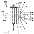
- FIG. 1 is a conceptual diagram of an example of an optical deflecting device of the present invention.
- FIG. 2 is a conceptual diagram of another example of the light deflection apparatus of the present invention.
- FIG. 3 is a conceptual diagram for explaining the operation of the optical deflection apparatus shown in FIG.
- FIG. 4 is a conceptual diagram of a liquid crystal optical phase modulation element.
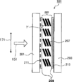
- FIG. 5 is a conceptual diagram of a liquid crystal diffraction element.
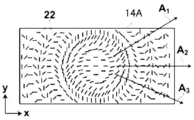
- FIG. 6 is a schematic plan view of the optically anisotropic layer.
- FIG. 7 is a conceptual diagram for explaining the action of the optically anisotropic layer.
- FIG. 8 is a conceptual diagram for explaining the action of the optically anisotropic layer.
- FIG. 9 is a conceptual diagram for explaining the action of the optically anisotropic layer.
- FIG. 10 is a schematic plan view of another example of the optically anisotropic layer.
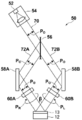
- FIG. 11 is a conceptual diagram of an exposure apparatus that exposes an alignment film.
- FIG. 12 is a conceptual diagram of another example of an exposure apparatus that exposes an alignment film.
- FIG. 13 is a conceptual diagram of another example of the light deflection apparatus of the present invention.
- FIG. 14 is a conceptual diagram of an optically anisotropic layer in an example of the present invention.
- FIG. 15 is a conceptual diagram of an optically anisotropic layer in an example of the present invention.
- FIG. 16 is a conceptual diagram for explaining the operation of an example of the optical deflecting device of the present invention.
- FIG. 17 is a diagram conceptually illustrating an example of the optical apparatus of the present invention.
- optical deflecting device of the present invention will be described below with reference to the drawings.
- the scale of the constituent elements is appropriately changed from the actual one for easy visual recognition.
- a numerical range expressed using “to” means a range including numerical values described before and after “to” as a lower limit value and an upper limit value.
- “orthogonal” and “parallel” with respect to the angle mean a range of a strict angle ⁇ 10 °.
- the optical deflecting device 100 of the present invention includes a condenser lens 131, a liquid crystal optical phase modulation element 101, a ⁇ / 4 plate 111, and an upstream side in the traveling direction of light (light beam).
- the liquid crystal optical phase modulation element 101 is an optical deflection element in the present invention, and is connected to a driving device 141.
- upstream and downstream are upstream and downstream in the light traveling direction.
- the ⁇ / 4 plate 111 and the liquid crystal diffraction element 121 are arranged on the emission side (downstream) of the liquid crystal optical phase modulation element 101, as shown in FIG. As shown in FIG. 1, the liquid crystal optical phase modulation element 101, the ⁇ / 4 plate 111, and the liquid crystal diffraction element 121 may be arranged in this section, or may be fixed using an adhesive or the like. Good.
- the liquid crystal optical phase modulation element 101, the ⁇ / 4 plate 111, and the liquid crystal diffraction element 121 are spaced so as not to deviate from the deflection angle of the light emitted from the liquid crystal optical phase modulation element 101.
- the same effect as that of the present invention can be obtained even if 102 is provided with a space.
- heat may be generated when passing, but by providing the interval 102, the heat generated by the light passing through the liquid crystal optical phase modulation element 101, the ⁇ / 4 plate 111, and ⁇ / 4
- the problem of melting the adhesive or the like that fixes the plate 111 and the liquid crystal diffraction element 121 can be avoided.
- the interval 102 is preferably 0.1 to 30 mm. In the case where the gap 102 is provided, the incident surface 103 of the liquid crystal diffraction element 121 is in contact with the air layer.
- FIG. 3 is a conceptual diagram for explaining the operation of the optical deflection apparatus 100 according to the embodiment of the present invention.
- the liquid crystal optical phase modulation element 101 deflects incident light 151 emitted from a light source (not shown) by a predetermined angle ⁇ ⁇ (see broken line).
- Incident light 151 is linearly polarized light in the direction indicated by arrow 171 in the figure.
- This linearly polarized light is P-polarized with respect to the exit surface 161 of the liquid crystal diffraction element 121 in the direction of polarization parallel to the cross-sectional view shown in FIG.
- S-polarized light may be used as the incident light 151. This can be dealt with by changing a part of the configuration of the liquid crystal optical phase modulation element 101.
- the maximum value of the variable range of the angle ⁇ in the liquid crystal optical phase modulation element 101 is defined as the maximum deflection angle ⁇ max, where the deflection angle ⁇ by the liquid crystal optical phase modulation element 101 is counterclockwise.
- the liquid crystal described later is set so that the emission angle when the light having the maximum deflection angle ⁇ max is incident on the liquid crystal diffraction element 121 becomes the target maximum emission angle ⁇ maxout in the optical deflecting device 10.
- the periodic structure pitch (rotation period p described later) in the optically anisotropic layer 14 of the diffraction element 121 is determined. In this way, even if the maximum deflection angle ⁇ max of the liquid crystal optical phase modulation element 101 is small, the maximum deflection angle ⁇ max by the liquid crystal optical phase modulation element 101 is set to the maximum target angle in the optical deflection apparatus 10 by the liquid crystal diffraction element 121. It becomes possible to expand to the emission angle ⁇ maxout. Similarly, when the angle ⁇ is in the negative direction, that is, clockwise, the maximum output angle of the light deflecting device 10 is the maximum output angle when the maximum deflection angle ⁇ max is the maximum value of the variable range of the angle ⁇ . By determining the periodic structure pitch so as to be the angle ⁇ maxout, the maximum deflection angle ⁇ max can be expanded to the target maximum emission angle ⁇ maxout even when the angle ⁇ is in the negative direction.
- the liquid crystal diffraction element 121 in order to increase the deflection angle of the emitted light, the liquid crystal diffraction element 121 gradually increases from the center of deflection (deflection azimuth) by the liquid crystal optical phase modulation element 101 toward the outside (both ends). Increase the diffraction angle.
- the periodic structure pitches (rotation periods p) of 121a, 121b, and 121c, which are regions of the liquid crystal diffraction element 121 are pa, pb, and pc
- the relationship of pa ⁇ pb ⁇ pc is established. Means there is.
- the periodic structure pitches of 121d and 121e are pd and pe, it means that there is a relationship of pe ⁇ pd ⁇ pc.
- the light is reduced by the liquid crystal diffraction element 121 when the angle ⁇ of the light emitted from the liquid crystal optical phase modulation element 101 is small.
- the periodic structure pitch is increased so as to be diffracted, and the period is such that the light is largely diffracted by the liquid crystal diffraction element 121 as the angle ⁇ of the light emitted from the liquid crystal optical phase modulation element 101 approaches the maximum deflection angle ⁇ max.
- the structure pitch is gradually reduced. In this way, the angle range of the outgoing light of the liquid crystal optical phase element is ⁇ ⁇ max, but when it exits from the liquid crystal diffraction element 121, it is expanded to ⁇ ⁇ maxout.
- the incident angle of light before entering the liquid crystal diffractive element 121 is ⁇ 1
- the refractive index of the incident side medium is n1
- the outgoing angle of light after exiting the liquid crystal diffractive element 121 is ⁇ 2
- the incident side of the medium on the outgoing side is Assuming that the refractive index is n2, the wavelength of light is ⁇ , the periodic structure pitch of the liquid crystal diffraction element is p, and the diffraction order is m, these values are related by the following equation (101).
- n1 ⁇ sin ⁇ 1 ⁇ n2 ⁇ sin ⁇ 2 m ⁇ ⁇ / p (101)
- the angle of light emitted from the liquid crystal diffraction element 121 can be changed by changing the periodic structure pitch p (rotation period p) of the liquid crystal diffraction element 121.
- the angle when finally emitted to the air can be up to an absolute value of about 80 °, so the angle ⁇ can be expanded to a very large angle.
- the periodic structure pitch of the liquid crystal diffraction element 121 that is, the rotation period p of the optically anisotropic layer 14, in the plane, light can be continuously emitted in an arbitrary direction.
- the optical deflecting device 100 includes the condensing lens 131, the liquid crystal optical phase modulation element 101, the ⁇ / 4 plate 111, and the liquid crystal as the condensing element in the present invention from the upstream side in the light traveling direction. And a diffraction element 121.
- the condensing lens 131 is a known condensing lens, and condenses light incident on the liquid crystal light phase modulation element 101 slightly. In the light deflection apparatus 100 of the present invention, the condensing lens 131 is provided as a preferred embodiment.
- the light deflecting device 100 includes the condenser lens 131, so that the light (light beam) emitted from the light deflecting device 100 (liquid crystal diffraction element 121) can be converted into appropriate parallel light, thereby improving straightness. .
- the action of the condenser lens 131 will be described in detail later.
- the condensing element is not limited to the condensing lens 131, and all known optical elements capable of condensing light (light beam) can be used.
- FIG. 4 is a cross-sectional view showing an example of the structure of the liquid crystal optical phase modulation element in the embodiment of the present invention.
- the liquid crystal optical phase modulation element exemplified here the liquid crystal optical phase modulation element of Example 1 of JP-A-2003-295153 is cited.
- the liquid crystal optical phase modulation element is not limited to the illustrated example, and any known liquid crystal optical phase modulation element used as an optical deflection element can be used.
- FIG. 1 Light deflection element
- a nematic liquid crystal layer 501 shown as an example of a liquid crystal layer includes an alignment layer 209 formed to cover the composite electrode 211 of the first transparent substrate 201 of the liquid crystal optical phase modulation element 101, and a second transparent substrate 203.
- the alignment layer 209 formed so as to cover the common electrode 213 is homogeneously aligned so that the tilt angle ⁇ of the director 207 of p-type (positive-type) liquid crystal molecules when no electric field is applied is 5 ° or less.
- the incident light 151 that is linearly polarized light in the direction indicated by the arrow 171 is set to be linearly polarized light parallel to the light deflection direction by the liquid crystal optical phase modulation element 101.
- the incident light 151 becomes P-polarized light when viewed from the exit surface 161 of the liquid crystal diffraction element 121.
- the first transparent substrate 201 and the second transparent substrate 203 are fixed via a spacer (not shown) so that the nematic liquid crystal layer 501 maintains a predetermined constant thickness of several ⁇ m to several tens of ⁇ m.
- a spacer not shown
- tantalum pentoxide, silicon dioxide, or the like is provided on at least one of the composite electrode 211 and the common electrode 213.
- a transparent insulating film may be formed. It is also desirable to improve the transmittance by forming the transparent insulating film into a multilayer film composed of a high refractive index film and a low refractive index film.
- the common electrode 213 formed on the second transparent substrate 203 may be a full-surface electrode made of a transparent conductive film.
- the number of liquid crystal optical phase modulation elements 101 is one.
- the present invention is not limited to this, and a plurality of such liquid crystal optical phase modulation elements 101 are provided. You may do it.
- the alignment direction of the liquid crystal cell may be either parallel or vertical. When the alignment direction of the liquid crystal cell is parallel, it contributes to increasing the maximum deflection angle ⁇ max, and contributes to the enlargement of the deflection angle by the liquid crystal optical phase modulation element 101, that is, the deflection angle by the optical deflecting device 100.
- a driving device 141 is connected to the liquid crystal optical phase modulation element 101.
- the driving device 141 is a known driving device that drives the liquid crystal optical phase modulation element 101 and that corresponds to the configuration of the liquid crystal optical phase modulation element 101.
- the ⁇ / 4 plate 111 is a known ⁇ / 4 plate (1/4 phase difference plate) that converts the linearly polarized light deflected by the liquid crystal optical phase modulation element 101 into circularly polarized light.
- ⁇ / 4 plate 111 a known one can be used without limitation. Therefore, the ⁇ / 4 plate 111 may be derived from a polymer or liquid crystal.
- FIG. 5 conceptually shows the liquid crystal diffraction element 121.
- FIG. 5 is a view of the liquid crystal diffraction element 121 as viewed in the same direction as FIGS. 1 to 3, and is a side view of the liquid crystal diffraction element 121.
- the liquid crystal diffraction element 121 is a sheet-like element, and includes the support 12, the alignment film 13, and the optically anisotropic layer 14.
- the liquid crystal diffraction element 121 further diffracts the light deflected by the liquid crystal optical phase modulation element 101 in the deflection direction of the liquid crystal optical phase modulation element, thereby further deflecting the light deflected by the liquid crystal optical phase modulation element 101.
- the deflection angle of the maximum emission angle ⁇ maxout which is much larger than the maximum deflection angle ⁇ max of the liquid crystal optical phase modulation element 101. Enables deflection of light.
- the sheet surface direction of the liquid crystal diffraction element 121 is defined as the xy direction and the thickness direction is defined as the z direction.
- the horizontal direction in the figure is the direction in which the optical axis derived from the liquid crystal compound rotates in one direction (the axis A direction described later), and this direction is the x direction.
- the y direction is a direction orthogonal to the paper surface of FIG. 1 to 3, the vertical direction in the drawing corresponds to the x direction, the direction orthogonal to the paper surface corresponds to the y direction, and the horizontal direction in the drawing corresponds to the z direction.
- the x direction coincides with the deflection direction by the liquid crystal optical phase modulation element 101. This also applies to FIG. 13 described later.
- the liquid crystal diffraction element 121 is planar, but the liquid crystal diffraction element 121 is not limited to a planar shape, and may be a curved surface.
- the support 12 is preferably a transparent support, and examples thereof include polyacrylic resin films such as polymethyl methacrylate, cellulose resin films such as cellulose triacetate, and cycloolefin polymer films.
- examples of the cycloolefin polymer film include a product name “Arton” manufactured by JSR Corporation, a product name “Zeonor” manufactured by Nippon Zeon Corporation, and the like.
- the support 12 may be a flexible film or may be a non-flexible substrate such as a glass substrate.
- the alignment film 13 is formed on the surface of the support 12.
- the alignment film 13 is an alignment film for aligning the liquid crystal compound 20 in a predetermined liquid crystal alignment pattern when forming the optically anisotropic layer 14.
- the optically anisotropic layer 14 is a liquid crystal in which the orientation of the optical axis 22 derived from the liquid crystal compound 20 changes while continuously rotating along one direction in the plane. Has an alignment pattern. Therefore, the alignment film 13 of the liquid crystal diffraction element 121 is formed so that the optically anisotropic layer 14 can form this liquid crystal alignment pattern.
- the optically anisotropic layer 14 of the liquid crystal diffractive element 121 in one direction (direction along an axis A described later) in which the direction of the optical axis 22 in the liquid crystal alignment pattern changes while continuously rotating, The length that the direction rotates 180 ° is defined as one period (the rotation period p of the optical axis 22).
- the optically anisotropic layer 14 gradually shortens one period from the center of deflection (deflection azimuth (deflection direction)) by the liquid crystal optical phase modulation element 101 to the outside.
- the rotation direction of the optical axis of the liquid crystal compound 20 is reversed at the center of deflection by the liquid crystal optical phase modulation element 101 in the direction along the axis A (arrow x direction). Therefore, the alignment film 13 of the liquid crystal diffraction element 121 is formed so that the optically anisotropic layer 14 can form this liquid crystal alignment pattern.
- the alignment film 13 various known ones can be used.
- the alignment film 13 of the optically anisotropic layer 14 include a rubbing treatment film made of an organic compound such as a polymer, an oblique deposition film of an inorganic compound, a film having a microgroove, and ⁇ -tricosanoic acid, dioctadecylmethyl.
- examples thereof include films obtained by accumulating LB (Langmuir-Blodgett) films of organic compounds such as ammonium chloride and methyl stearylate by the Langmuir-Blodgett method.
- the alignment film 13 include those formed by rubbing the surface of the polymer layer.
- the rubbing treatment is performed by rubbing the surface of the polymer layer several times in a certain direction with paper or cloth.
- the types of polymers used for the alignment film are polyimide, polyvinyl alcohol, polymers having a polymerizable group described in JP-A-9-152509, JP-A-2005-97377, JP-A-2005-99228, and Further, an orthogonal alignment film described in JP-A-2005-128503 can be preferably used.
- the term “orthogonal alignment film” as used in the present invention means an alignment film that aligns the major axis of the molecules of the polymerizable rod-like liquid crystal compound of the present invention so as to be substantially orthogonal to the rubbing direction of the orthogonal alignment film.
- the thickness of the alignment film does not need to be large as long as it can provide an alignment function, and is preferably 0.01 to 5 ⁇ m, and more preferably 0.05 to 2 ⁇ m.
- a so-called photo-alignment film which is an alignment film by irradiating a photo-alignment material with polarized light or non-polarized light, can also be used. That is, a photo-alignment film may be produced by applying a light distribution material on the support 12. Irradiation with polarized light can be performed in a vertical direction or an oblique direction with respect to the photo-alignment film, and irradiation with non-polarized light can be performed in an oblique direction with respect to the photo-alignment film.
- Examples of the photo-alignment material used in the photo-alignment film that can be used in the present invention include, for example, JP-A-2006-285197, JP-A-2007-76839, JP-A-2007-138138, and JP-A-2007-94071.
- FIG. 11 shows a schematic diagram of an alignment film exposure apparatus that applies a photo-alignment material on the support 12 and dries it, and then exposes the alignment film to form an alignment pattern.
- the exposure apparatus 50 includes a light source 54 including a laser 52, a beam splitter 56 that separates the laser light 70 from the laser 52 into two, and mirrors disposed on the optical paths of the two separated light beams 72A and 72B. 58A, 58B and ⁇ / 4 plates 60A, 60B.
- the light source 64 includes, for example, a polarizing plate and emits linearly polarized light P 0 .
- lambda / 4 plate 60A and 60B is provided with an optical axes perpendicular to one another, lambda / 4 plate 60A is linearly polarized light P 0 on the right circularly polarized light P R, lambda / 4 plate 60B is left circularly linearly polarized light P 0 converting the polarization P L.
- the support 12 having the alignment film 13 before the alignment pattern is formed is disposed in the exposure portion, and the two light beams 72A and 72B are crossed on the alignment film 13 to interfere with each other. Irradiate and expose. Due to the interference at this time, the polarization state of the light applied to the alignment film 13 periodically changes in the form of interference fringes. Thereby, an alignment pattern in which the alignment state changes periodically can be obtained.
- the period of the alignment pattern can be changed by changing the crossing angle ⁇ of the two light beams 72A and 72B. That is, in the exposure apparatus 50, in the alignment pattern in which the optical axis 22 derived from the liquid crystal compound 20 continuously rotates along one direction by adjusting the crossing angle ⁇ , the optical axis 22 rotates in one direction.
- the length of one period (rotation period p) by which the optical axis 22 rotates 180 ° can be adjusted.
- an optically anisotropic layer 14 to be described later on the alignment film 13 having an alignment pattern in which the alignment state is periodically changed in this way, an optical anisotropy having a liquid crystal alignment pattern corresponding to this period is formed.
- Layer 14 can be formed.
- the rotation direction of the optical shaft 22 can be reversed by rotating the optical axes of the ⁇ / 4 plate 60A and the ⁇ / 4 plate 60B by 90 °. Accordingly, masking is performed on the half surface of the alignment film 13 to perform exposure, then masking is performed on the exposed area, and the optical axes of the ⁇ / 4 plate 60A and the ⁇ / 4 plate 60B are rotated by 90 °, respectively.
- the rotation direction of the optical axis 22 can be reversed at the center.
- the length of one cycle in which the optical axis 22 rotates 180 ° (rotation cycle p) ) Can be gradually shortened from the center of one direction in which the optical axis 22 rotates toward the outside.
- An exposure apparatus 80 conceptually shown in FIG. 12 is also preferably used for exposing the alignment film 13.
- An exposure apparatus 80 shown in FIG. 12 is an exposure apparatus that is also used when forming a concentric liquid crystal alignment pattern as shown in FIG.
- the exposure apparatus 80 includes a light source 84 including a laser 82, a polarization beam splitter 86 that divides the laser light M from the laser 82 into S-polarized MS and P-polarized MP, and a mirror 90A disposed in the optical path of the P-polarized MP.
- a mirror 90B disposed in the optical path of S-polarized MS, a lens 92 (convex lens) disposed in the optical path of S-polarized MS, a polarization beam splitter 94, and a ⁇ / 4 plate 96.
- the P-polarized light MP divided by the polarization beam splitter 86 is reflected by the mirror 90A and enters the polarization beam splitter 94.
- the S-polarized light MS divided by the polarization beam splitter 86 is reflected by the mirror 90B, collected by the lens 92, and incident on the polarization beam splitter 94.
- the P-polarized light MP and the S-polarized light MS are combined by the polarization beam splitter 94 to become right circularly polarized light and left circularly polarized light according to the polarization direction by the ⁇ / 4 plate 96, and the alignment film 13 on the support 12. Is incident on.
- the polarization state of the light applied to the alignment film 13 periodically changes in the form of interference fringes.
- the crossing angle of the left circularly polarized light and the right circularly polarized light changes, so that an exposure pattern whose pitch changes from the inside to the outside can be obtained.
- the alignment film 13 a concentric alignment pattern in which the alignment state changes periodically is obtained.
- the length of one period (rotation period p) in which the optical axis 22 of the liquid crystal compound 20 continuously rotates 180 ° along one direction is the refractive power of the lens 92 (F number of the lens 92). It can be controlled by changing the focal length of the lens 92, the distance between the lens 92 and the alignment film 13, and the like. Further, by adjusting the refractive power of the lens 92 (F-number of the lens 92), the length of one cycle in which the optical shaft 22 rotates 180 ° can be changed in one direction in which the optical shaft 22 rotates continuously.
- the length of one cycle in which the optical axis 22 rotates by 180 ° can be changed according to the degree of condensing of the light transmitted through the lens 92 that interferes with the parallel light. More specifically, when the refractive power of the lens 92 is weakened, it approaches parallel light, so that the length of one cycle in which the optical axis 22 rotates 180 ° gradually decreases from the inside toward the outside, and the F number is growing. On the contrary, when the refractive power of the lens 92 is increased, the length of one period in which the optical axis 22 rotates 180 ° is suddenly shortened from the inside toward the outside, and the F number is reduced.
- a configuration in which the optical axis 22 of the liquid crystal compound 20 continuously rotates and changes only in the direction can also be used.
- an optical element that transmits light so as to be condensed can be obtained.
- an optical element that transmits light so as to diffuse only in the arrow X direction can be obtained.
- An optical element that transmits light so as to diffuse only in the X direction of the arrow can also be obtained by reversing the turning direction of the incident circularly polarized light. Further, depending on the use of the optical element, for example, when it is desired to provide a light amount distribution in the transmitted light, one cycle in which the optical axis 22 rotates 180 degrees toward the arrow X direction is not gradually changed, but in the arrow X direction. Also, a configuration in which the optical axis 22 is partially rotated by 180 ° and has a region with different one cycle can be used.
- a method of scanning and patterning the photo-alignment film while arbitrarily changing the polarization direction of the condensed laser light is used. be able to.
- the alignment film 13 is provided as a preferred embodiment and is not an essential component.
- the optically anisotropic layer 14 is derived from the liquid crystal compound 20 by forming an alignment pattern on the support 12 by a method of rubbing the support 12, a method of processing the support 12 with a laser beam, or the like. It is also possible to adopt a configuration having a liquid crystal alignment pattern in which the orientation of the optical axis 22 is changed while continuously rotating along at least one in-plane direction.
- an optically anisotropic layer 14 that is a cured layer of a liquid crystal composition containing the liquid crystal compound 20 is provided on the surface of the alignment film 13.
- the optical axis (slow axis) of the liquid crystal compound is a liquid crystal pattern arranged along at least one direction in the plane of the optically anisotropic layer, and the optical axis of the liquid crystal compound 20.
- the direction of the axis 22 has a liquid crystal alignment pattern that is rotationally changed in one direction.
- the retardation R is preferably 0.4 ⁇ to 0.6 ⁇ , more preferably 0.45 ⁇ to 0.55 ⁇ , and particularly preferably 0.5 ⁇ .
- ⁇ n is the birefringence of the optically anisotropic layer 14
- d 1 is the thickness.
- the retardation R for light of 940 nm may be in the range of 338 to 602 nm, and is particularly preferably 470 nm.
- the liquid crystal diffraction element 121 functions as a transmission type diffraction grating.
- the principle of functioning as a diffraction grating will be described with reference to FIGS. 6 is a schematic plan view of the optically anisotropic layer 14, that is, FIG. 5 is a view of the optically anisotropic layer 14 as viewed from above.
- the liquid crystal compound 20 is fixed in a liquid crystal alignment pattern in which the optical axis 22 is continuously rotated in one direction.
- the optical axis 22 continuously rotates and changes in the direction along the axis A in FIG.
- the liquid crystal compound 20 is aligned so that the angle formed by the axis A and the in-plane component of the major axis (abnormal light axis: director) of the liquid crystal compound 20 defined as the optical axis 22 changes. .
- the direction of the optical axis 22 of the liquid crystal compound 20 is the same in the liquid crystal compound 20 aligned in the direction orthogonal to the axis A, that is, in the arrow y direction. Yes.
- the optically anisotropic layer 14 exhibits a function as a general ⁇ / 2 plate as described above for each region in which the direction of the optical axis 22 of the liquid crystal compound 20 in the y direction coincides.
- the angle formed between the optical axis 22 and the axis A of the liquid crystal compound 20 arranged along the axis A differs from the liquid crystal alignment pattern in which the direction of the optical axis 22 is rotated and changed depending on the position in the axis A direction.
- the pattern is oriented and fixed so that the angle formed by the optical axis 22 and the axis A along the axis A gradually changes from ⁇ to ⁇ + 180 ° or ⁇ 180 °.
- the optical axis 22 of the liquid crystal compound 20 is parallel to the surface of the optically anisotropic layer 14, and the direction of the optical axis 22 is constant.
- a local region that is, a region in which the liquid crystal compound 20 is arranged in the arrow y direction is arranged in the x direction orthogonal to the arrow y direction, and between the plurality of local regions arranged in the arrow x direction.
- the liquid crystal alignment pattern in which the orientation of the optical axis 22 is continuously rotated in one direction (the direction along the axis A) is referred to as horizontal rotational alignment.
- the change in the angle of the optical axis 22 in the direction of the axis A may be an object that rotates at nonuniform angular intervals instead of a constant angular interval.
- the average value of the direction of the optical axis 22 in the unit region is linearly changed at a constant rate, it is gradually changed.
- the change in the inclination of the optical axis between the unit regions adjacent to each other in the direction of the axis A and having different inclinations of the optical axis 22 is 45 ° or less.
- the change in the inclination of the adjacent unit region is preferably smaller.
- the rotation period p is preferably 0.5 to 5 ⁇ m. The shorter the rotation period p, the larger the diffraction angle by the optically anisotropic layer 14, that is, the liquid crystal diffraction element 121. Therefore, the rotation period p may be determined according to the wavelength of the incident light to the liquid crystal diffraction element 121 and a desired emission angle.
- the liquid crystal diffraction element 121 gives a phase difference of ⁇ / 2 to the incident light, and enters the incident light at an incident angle of 0 °, that is, vertically incident light. emit at theta 2. That is, as shown in FIG. 7 to be described later, when light is incident L 1 side in vertical right circular polarization P R of the optically anisotropic layer 14, left circular polarization in the direction forming an normal direction and the angle theta 2 P L light L 2 is emitted.
- that light is incident on the surface of the optically anisotropic layer 14 perpendicularly means that light is incident along the normal of the surface.
- the light L 1 of the right circularly polarized light P R incident on the optical anisotropic layer 14 is also referred to as “incident light L 1 ”.
- the light L 2 of the left circularly polarized light P L emitted from the optically anisotropic layer is also referred to as “emitted light L 2 ”.
- Liquid crystal diffraction element 121 case of incident light of a predetermined wavelength, as the rotation period p in the optically anisotropic layer 14 is small, the emission angle of the diffraction angle or the outgoing light L 2 is increased.
- the exit angle of the outgoing light L 2 is the angle formed by the normal direction of the optically anisotropic layer 14 and the outgoing light L 2 is.
- the diffraction direction of the outgoing light L 2 from the liquid crystal diffraction element 121 is the circular polarization of the light incident on the liquid crystal diffraction element 121.
- the incident is controlled. That is, when the incident light is linearly polarized light as shown in the example, the ⁇ / 4 plate 111 is inserted and converted to either the left or right circularly polarized light, so that the incident direction of light diffraction can be changed. Can only be.
- FIG. 7 is a diagram schematically showing the principle that incident light L 1 perpendicularly incident on the optically anisotropic layer 14 is emitted at a predetermined emission angle ⁇ 2 .
- incident light L 1 perpendicularly incident on the optically anisotropic layer 14 is emitted at a predetermined emission angle ⁇ 2 .
- the incident light L 1 is a right circularly polarized light P R, by passing through the optically anisotropic layer 14, a phase difference of lambda / 2 is converted given to left-handed circularly polarized light P L.
- the incident light L 1 is the optical axis 22 of the liquid crystal compound 20 in each unit region in a plane (local area), the absolute phase changes.
- the orientation of the optical axis 22 of the liquid crystal compound 20 changes by rotating toward the axis A direction (in this example, the direction of the arrow x), so that the incident light
- the amount of change in the absolute phase varies depending on the direction of the optical axis 22 of the liquid crystal compound 20 at the x coordinate (the position in the x direction) of the surface (xy plane) of the optically anisotropic layer 14 on which is incident.
- a region indicated by a broken line in FIG. 7 schematically shows that the change amount of the absolute phase varies depending on the x coordinate. As shown in FIG.
- an absolute phase equiphase surface 24 having an angle with respect to the surface of the optically anisotropic layer is formed by the deviation of the absolute phase when passing through the optically anisotropic layer 14.
- the incident light L 1 incident from the normal direction the bending force is applied in a direction perpendicular to the equiphase plane 24, the traveling direction of the incident light L 1 is changed. That is, the incident light L 1 is a right circularly polarized light P R, the after passing through the optically anisotropic layer 14 left-handed circularly polarized light P L becomes and proceeds to a direction forming a normal direction at a predetermined angle theta 2 It is emitted from the optically anisotropic layer 14 as an outgoing light L 2.
- the liquid crystal in the diffraction element 121 As described above, the liquid crystal in the diffraction element 121, the incident light L 1 incident along the normal direction perpendicular to the plane of the liquid crystal diffraction element 121, output light L 2 in a direction different from the normal direction Is emitted.
- the inclination of the emission angle can be changed by changing the rotation period p in the direction of the optical axis in the liquid crystal alignment pattern in the optical anisotropic layer 14. As the rotation period P is decreased, a larger bending force can be applied to the incident light, so that the inclination can be increased.
- the wavefront of the incident light can be changed by changing the amount of change in absolute phase by the liquid crystal alignment pattern in the optically anisotropic layer 14.
- the conversion of the incident light L 1 to the outgoing light L 2 based on the above principle is transmission diffraction.
- Optically anisotropic layer 14 with respect to the incident light L 1 acts as a transmission grating, the incident light L 1 which is perpendicularly incident on the optically anisotropic layer 14, predetermined diffraction angle theta 2 of the emitted light (transmitted diffraction light) It is transmitted diffracted as L 2.
- equation (1) which is a general light diffraction equation, is satisfied.
- n 1 is the refractive index of the medium 1 on the incident surface side of the diffraction grating (here, the optically anisotropic layer 14), ⁇ 1 is the incident angle, and n 2 is the diffraction grating (here, the optically anisotropic layer).
- the refractive index of the medium 2 on the exit surface side, ⁇ 2 is the diffraction angle (exit angle), ⁇ is the wavelength, p is the rotation period, and m is the order of diffraction.
- FIG. 8 is a diagram schematically illustrating the diffraction phenomenon represented by the equation (2).
- An optically anisotropic layer 14 as a diffraction grating is disposed between the medium n 1 and the medium n 2 .
- Light L 1 incident on the optically anisotropic layer 14 from the normal direction from the medium 1 side is a refractive index n 1 is diffracted by the diffraction effect of the optically anisotropic layer 14, the refractive index n 2 medium 2 Emitted to the side.
- the emitted light L 2 emitted by the emission angle theta 2 time can be rephrased as transmitted diffraction light L 2 of the diffraction angle theta 2.
- the optically anisotropic layer 14 in which the liquid crystal compound 20 is horizontally rotated and fixed functions as a diffraction grating.
- the wavelength ⁇ of the light that causes the diffraction action by the liquid crystal diffraction element 121 may be from ultraviolet to visible light, infrared, or even an electromagnetic wave level.
- the diffraction angle increases as the wavelength of incident light increases, and the diffraction angle decreases as the wavelength of incident light decreases.
- the liquid crystal compound 20 a rod-like liquid crystal compound and a disk-like liquid crystal compound can be used.
- the wavelength ⁇ is 380 nm
- the disc-shaped liquid crystal compound can obtain higher diffraction efficiency than the rod-shaped liquid crystal compound when the rotation period p ( ⁇ m) is in the range of 0.5 ⁇ p ⁇ 1.
- the wavelength ⁇ is 1100 nm
- the discotic liquid crystal compound can obtain higher diffraction efficiency than the rod-shaped liquid crystal compound when the rotation period p ( ⁇ m) is in the range of 2 ⁇ p ⁇ 5.
- the liquid crystal diffraction element 121 (optically anisotropic layer 14), if the light is incident L 41 of randomly polarized light, among the incident light L 41, right circularly polarized light P R As described above, this component is converted into left circularly polarized light P L in the optically anisotropic layer 14, undergoes a bending force due to the liquid crystal alignment pattern, changes its traveling direction, passes through the optically anisotropic layer, It is emitted as transmitted diffraction light L 42 1.
- components of the left circularly polarized light P L of the incident light L 41 together are converted into right circularly polarized light P R in the optically anisotropic layer 14 was converted from right circularly polarized light into left-handed circularly polarized light
- the light travels through the optical anisotropic layer 14 in a changed state, and is emitted as the second transmitted diffracted light L 43 from the opposite surface of the liquid crystal diffraction element 121.
- the traveling directions of the first transmitted diffracted light L 42 and the second transmitted diffracted light L 43 are substantially axisymmetric with respect to the normal line.
- the rotation period may be designed so as to obtain a desired diffraction angle ⁇ 2 so as to satisfy the above formula (1) in consideration of the incident angle ⁇ 1 .
- the optical deflecting device 100 of the present invention refracts (diffracts) the light deflected by the liquid crystal optical phase modulation element 101 by the liquid crystal diffraction element 121 (optical anisotropic layer 14), so that the liquid crystal optical phase.
- the light can be deflected by the deflection angle of the maximum emission angle ⁇ maxout which is much larger than the maximum deflection angle ⁇ max of the modulation element 101.
- the refraction (diffraction angle) of light by the optically anisotropic layer 14 increases as one period in which the optical axis 22 of the liquid crystal compound 20 rotates 180 °, that is, the rotation period p is shorter.
- the polarization direction (swing direction) of the incident circularly polarized light is the same, the light refraction direction by the optical anisotropic layer 14 is reversed depending on the rotation direction of the optical axis 22 of the liquid crystal compound 20. That is, when the incident light L 1 is a right circularly polarized light P R, as viewed from the exit surface side, the rotational direction of the optical axis 22, in the axial direction A (direction of arrow x) as shown in FIGS. 5 to 7 When it is clockwise, the outgoing light L2 is refracted in the direction of the axis A, for example.
- the optical anisotropic layer 14 deflects the rotation period p of the optical axis 22 of the liquid crystal compound 20 in the direction of the axis A by the liquid crystal optical phase modulation element 101 (
- the deflection direction is gradually shortened from the center to the outside. That is, the amount of light refracted by the optically anisotropic layer 14 increases toward the outside in the deflection direction.
- the optical anisotropic layer 14 has the rotational direction of the optical axis 22 of the liquid crystal compound 20 directed in the direction of the axis A at the center of deflection by the liquid crystal optical phase modulation element 101. Reverse.
- the optical deflection apparatus 100 of the present invention enables light deflection by the deflection angle of the maximum emission angle ⁇ maxout that is much larger than the maximum deflection angle ⁇ max of the liquid crystal optical phase modulation element 101. ing.
- the direction of rotation of the optical axis 22 is usually reversed at the center of the optical anisotropic layer 14 in the direction of the axis A (arrow x direction), that is, the direction in which the optical axis 22 rotates. That is, in the optical deflecting device 100, the center of deflection in the liquid crystal optical phase modulation element 101 and the center in the axis A direction in the optical anisotropic layer 14 are usually matched.
- the rotation period p may be continuously shortened from the center of deflection toward the outside, or may be shortened stepwise.
- the optically anisotropic layer 14 is formed of a liquid crystal composition containing a liquid crystal compound.
- the liquid crystal composition containing a liquid crystal compound for forming the optically anisotropic layer 14 contains other components such as a leveling agent, an alignment controller, a polymerization initiator and an alignment aid in addition to the liquid crystal compound. May be.
- An optically anisotropic layer in which a predetermined liquid crystal alignment pattern is fixed, comprising a cured layer of a liquid crystal composition by forming an alignment film on a support and applying and curing the liquid crystal composition on the alignment film Can be obtained.
- each component of the liquid crystal composition of the present invention will be described in detail.
- the optically anisotropic layer 14 is a cured layer of a liquid crystal composition containing a rod-like liquid crystal compound or a discotic liquid crystal compound, and the optical axis of the rod-like liquid crystal compound or the optical axis of the discotic liquid crystal compound is aligned as described above. It has a liquid crystal alignment pattern.
- an optically anisotropic layer composed of a cured layer of the liquid crystal composition can be obtained.
- the optically anisotropic layer functions as a so-called ⁇ / 2 plate
- the present invention includes a mode in which a laminated body integrally including the support 12 and the alignment film functions as a ⁇ / 2 plate. .
- the liquid crystal composition for forming the optically anisotropic layer contains a rod-like liquid crystal compound or a disk-like liquid crystal compound, and other components such as a leveling agent, an alignment controller, a polymerization initiator, and an alignment aid. May be contained.
- the optically anisotropic layer preferably has a wide band with respect to the wavelength of incident light, and is preferably formed using a liquid crystal material having a birefringence index that is inversely dispersed. Furthermore, it is also preferable to make the optically anisotropic layer substantially broadband with respect to the wavelength of incident light by imparting a twisting component to the liquid crystal composition and by laminating different retardation layers.
- Japanese Unexamined Patent Application Publication No. 2014-089476 discloses a method for realizing a broadband ⁇ / 2 plate by laminating two liquid crystal layers having different twist directions in an optically anisotropic layer. Can be preferably used in the present invention.
- rod-like liquid crystal compounds examples include azomethines, azoxys, cyanobiphenyls, cyanophenyl esters, benzoic acid esters, cyclohexanecarboxylic acid phenyl esters, cyanophenylcyclohexanes, cyano-substituted phenylpyrimidines, alkoxy-substituted phenylpyrimidines, Phenyldioxanes, tolanes, and alkenylcyclohexylbenzonitriles are preferably used.
- high-molecular liquid crystalline molecules can also be used.
- the polymerizable rod-like liquid crystal compound examples include those described in Makromol. Chem. 190, 2255 (1989), Advanced Materials, 5, 107 (1993), US Pat. No. 4,683,327, US Pat. No. 5,622,648, US Pat. No. 5,770,107, International Publication No. 95/22586, 95/24455, 97/00600, 98/23580, 98/52905, JP-A-1-272551, 6-16616, 7-110469, 11-80081 And the compounds described in Japanese Patent Application No. 2001-64627 and the like can be used. Further, as the rod-like liquid crystal compound, for example, those described in JP-A-11-513019 and JP-A-2007-279688 can be preferably used.
- the discotic liquid crystal compound for example, those described in JP-A-2007-108732 and JP-A-2010-244038 can be preferably used.
- the liquid crystal compound 20 rises in the thickness direction in the optically anisotropic layer, and the optical axis 22 derived from the liquid crystal compound has a disc surface. It is defined as an axis perpendicular to the so-called fast axis.
- the optically anisotropic layer 14 can be formed by applying a multilayer liquid crystal composition on the alignment film 13.
- a liquid crystal composition is applied on an alignment film, heated, cooled, and then cured with ultraviolet rays to produce a first liquid crystal immobilization layer. It refers to repeating coating by coating on the chemical layer, heating in the same manner, and performing UV curing after cooling.
- the light deflection apparatus 100 in the illustrated example includes the condenser lens 131 on the upstream side of the liquid crystal optical phase modulation element 101 as a preferable aspect.
- the refraction of light by the optically anisotropic layer 14 gradually increases from the center in the deflection direction to the outside.
- the light deflected by the optical deflecting device 100 that is, the light beam actually has a thickness.
- the amount of light refracted by the optically anisotropic layer 14 is strictly different between the inside (the center of deflection) and the outside in the deflection direction, and the outside is larger in the amount of refraction.
- the light refracted by the liquid crystal diffraction element 121 becomes light that expands slightly so as to diffuse.
- the condenser lens 131 is provided, and the light incident on the liquid crystal diffractive element 121 is made to have a slightly reduced diameter, so that the light emitted from the light deflecting device 100 (liquid crystal diffractive element 121) is parallel. It is possible to improve straightness by using light. As a result, by providing the condensing lens 131, the light scanning by the light deflecting device 100 can be accurately performed even if the object to be scanned by the light is far from the light deflecting device 100.
- the refractive power (lens power) of the condenser lens 131 is not limited. That is, the refractive power of the condensing lens 131 includes the amount of light refracted by the liquid crystal diffraction element 121 and its in-plane distribution (that is, the in-plane distribution function of the diffraction pitch), the light deflection angle by the light deflecting device 100, and the light deflecting device.
- the refractive power capable of emitting suitable light may be set as appropriate according to the distance between 100 and the optical scanning target, the light diameter (beam diameter) of incident light, and the like.
- the position of the condenser lens 131 may be upstream from the liquid crystal diffraction element 121. However, the liquid crystal optical phase can be reduced in that the condenser lens 131 can be downsized and the condenser lens 131 can be easily designed. It is preferable to be upstream of the modulation element 101 (light deflection element).
- FIG. 10 is a schematic plan view of an optically anisotropic layer in a design change example of the liquid crystal diffraction element.
- the liquid crystal alignment pattern in the optically anisotropic layer 14A shown in FIG. 10 is different from the liquid crystal alignment pattern in the optically anisotropic layer 14 described above. In FIG. 10, only the optical axis 22 is shown.
- the optically anisotropic layer 14A in FIG. 10 is a liquid crystal in which the orientation of the optical axis 22 is changed by gradually rotating along multiple directions from the center side to the outer side, for example, the axes A 1 , A 2 , A 3 . It has an orientation pattern. That is, the liquid crystal alignment pattern of the optically anisotropic layer 14A shown in FIG.
- the liquid crystal alignment pattern of the optically anisotropic layer 14A shown in FIG. 10 is a concentric pattern having one direction in which the direction of the optical axis changes while continuously rotating, concentrically from the inside toward the outside. It is.
- the absolute phase of incident light changes with different amounts of change between local regions in which the direction of the optical axis 22 is different. If a liquid crystal alignment pattern whose optical axis rotates in a radial manner as shown in FIG. 10 is provided, the incident light can be transmitted as diverging light or condensed light. That is, the function as a concave lens or a convex lens can be realized by the liquid crystal alignment pattern in the optical anisotropic layer 14.
- the center of the lens when aligned with the center of the light emitted from the liquid crystal light phase modulation element 101, the light can be spread most efficiently at the maximum deflection angle ⁇ max emitted from the liquid crystal light phase modulation element.
- the light deflecting device of the present invention can deflect light so as to diffuse radially from the center by using the function of the concave lens of the optically anisotropic layer 14A shown in FIG. 10 for the liquid crystal diffraction element 121A.
- a deflection element 101A is used.
- the light deflection element 101A deflects light at an azimuth of 360 ° and a polar angle of 0 to 35 °.
- the light L deflected radially by the light deflecting element 101A is refracted by the liquid crystal diffractive element 121A, so that the deflection angle, that is, the azimuth angle by the light deflecting element 101A is expanded, and a wide range is obtained.
- the light can be deflected radially.
- a condensing lens 131 is provided as a preferred embodiment.
- the condenser lens 131 By the condenser lens 131, the light L is incident on the light deflecting element 101A as the condensed light, deflected, and directly incident on the liquid crystal diffractive element 121A as the condensed light, so that the light refracted by the liquid crystal diffractive element 121A is collimated. It can be deflected and emitted as light.
- a MEMS (Micro Electro Mechanical Systems) optical deflecting element described in Japanese Patent Laid-Open No. 2012-208352 is disclosed as an example.
- a mirror By oscillating a mirror (mirror) using a piezoelectric actuator or the like, such as a MEMS optical deflecting element described in 134642 and a MEMS optical deflecting element described in JP-A-2015-22064, light is emitted.
- MEMS optical deflection elements MEMS (optical) scanners, MEMS optical deflectors, MEMS mirrors, DMDs (Digital Micromirror Devices)) that perform deflection (deflection scanning).
- the liquid crystal compound 20 of the liquid crystal diffraction element is oriented in one direction in the thickness direction, but the present invention is not limited to this.
- the optical anisotropic layers constituting the liquid crystal diffraction element are the same as the first optical anisotropic layer 215 and the second optical anisotropic layer 216 of the liquid crystal diffraction element 220 shown in FIG.
- the liquid crystal compound 20 may be twisted and aligned along a helical axis extending along the thickness direction. In the following description, the twist orientation along the helical axis extending along the thickness direction is also simply referred to as “twist orientation”.
- the first optical anisotropic layer 215 and the second optical anisotropic layer 216 in which the liquid crystal compound 20 is twisted and aligned are cross sections obtained by observing the cross section of the liquid crystal diffraction element 220 with a scanning electron microscope (SEM).
- SEM scanning electron microscope
- the optical axis of the liquid crystal compound when the optical axis of the liquid crystal compound is gradually shortened in the direction in which the optical axis 22 rotates by one period (rotation period p) that rotates 180 degrees,
- the inclination angle of the bright and dark lines with respect to the normal line of the first optical anisotropic layer 215 and the second optical anisotropic layer 216 gradually decreases in the direction in which the optical axis 22 rotates. That is, in this case, the inclination angle of the bright and dark lines rises with respect to the main surface of the optically anisotropic layer.
- the bright and dark line patterns of the first optical anisotropic layer 215 and the second optical anisotropic layer 216 have a shorter period in the direction in which the optical axis 22 rotates.
- the diffraction efficiency of light can be improved even with high-angle diffraction.
- the light amount in the optically anisotropic layer can be suppressed and the amount of emitted light can be improved.
- the first optical anisotropic layer 215 and the second optical anisotropic layer 216 have different twist directions in the twist alignment of the liquid crystal compound 20. That is, in the first optical anisotropic layer 215, the liquid crystal compound 20 is twisted and oriented clockwise in the light traveling direction. On the other hand, in the second optical anisotropic layer 216, the liquid crystal compound 20 is twisted and oriented counterclockwise in the light traveling direction. Therefore, the first optically anisotropic layer 215 and the second optically anisotropic layer 216 have different inclination directions of bright and dark lines derived from the twisted orientation in the cross-sectional SEM image.
- first optically anisotropic layer 215 for example, when the incident light is right circularly polarized light, the diffraction efficiency is improved for light traveling toward the left side (outside) in the figure indicated by the solid line. Great effect is obtained.
- the first optically anisotropic layer 215 improves the diffraction efficiency for light traveling toward the right side (center side) in the drawing indicated by the broken line, for example, when the incident light is right circularly polarized light. The effect is small.
- the second optical anisotropic layer 216 when the incident light is right circularly polarized light, on the contrary, the diffraction efficiency is improved with respect to the light traveling toward the left side (outside) in the figure indicated by the solid line.
- the effect is small.
- the second optically anisotropic layer 216 has a great effect of improving the diffraction efficiency with respect to light traveling toward the right side (center side) in the drawing indicated by the broken line. This effect is reversed when the incident light is left circularly polarized light.
- the liquid crystal diffraction element 220 In the liquid crystal diffraction element 220, only light traveling toward the left side (outer side) in the figure indicated by the solid line enters the region shown in FIG. 14 where the center of deflection is on the right side in the figure. Therefore, in this light (right circularly polarized light), that is, in the region on the left side in the figure from the center, the first optical anisotropic layer 215 acts strongly, improving the diffraction efficiency and increasing the amount of emitted light. . On the other hand, in the region on the right side of the center with respect to the region shown in FIG. 14, only the light traveling toward the right side in the drawing indicated by the broken line is incident.
- the second optical anisotropic layer 216 acts strongly on this light (right circularly polarized light), improving the diffraction efficiency and increasing the amount of emitted light. Further, since the incident angle of incident light with respect to the optical anisotropic layer is small in the central region of the polarized light, both the first optical anisotropic layer 215 and the second optical anisotropic layer 216 improve the diffraction efficiency. Contribute. As a result, according to the liquid crystal diffraction element 220 having the first optical anisotropic layer 215 and the second optical anisotropic layer 216 in which the twist directions in the twist alignment of the liquid crystal compound 20 are different from each other, the entire region in the light deflection direction. The effect of improving the diffraction efficiency can be obtained, and a large amount of light can be emitted over the entire deflection angle.
- the twist angle of the liquid crystal compound is not limited. What is necessary is just to set suitably the twist angle of a liquid crystal compound according to the deflection angle by an optical deflection element, the target diffraction efficiency, etc.
- the twist angle of the liquid crystal compound 20 is preferably 10 to 200 °, more preferably 20 to 190 °, and still more preferably 40 to 170 °.
- the twist angle (twist angle in the thickness direction) of the liquid crystal compound 20 that is twist-oriented is the twist angle of the liquid crystal compound 20 that is twist-aligned along the helical axis extending in the thickness direction in the optically anisotropic layer. This is the twist angle from the lower surface to the upper surface.
- the liquid crystal diffraction element having the first optical anisotropic layer 215 and the second optical anisotropic layer 216 in which the liquid crystal compound 20 is twisted and twisted in a spiral shape is like a liquid crystal diffraction element 224 shown in FIG.
- the liquid crystal compound 20 may have a third optical anisotropic layer 219 in which the twisted orientation is not performed.
- the third optical anisotropic layer 219 in which the liquid crystal compound is not twisted and aligned is a non-tilted optical anisotropic layer in which bright and dark lines extend along the normal direction.
- liquid crystal diffraction element 121 has been described as a transmission type diffraction element, a reflection type liquid crystal diffraction element can also be used in the optical deflection apparatus of the present invention. In that case, the same formation method can be adopted only by changing the liquid crystal composition.
- a cholesteric liquid crystal as the liquid crystal and using an alignment film similar to the transmission type, reflection type diffracted light can be generated and used for angle expansion.
- a light reflecting element that reflects light in a direction different from the incident angle, it can be applied as a condensing mirror for a sensor as a micromirror that collects or diverges light, or as a microlens.
- the optical deflection element is not limited to the liquid crystal optical phase modulation element 101, and various known optical deflection elements such as a galvano mirror, a polygon mirror, and a MEMS optical deflection element can be used. It is. Among them, the liquid crystal optical phase modulation element 101 and the MEMS optical deflection element described above are preferably used as the optical deflection element in that the mechanical movable part is small and the mechanical movable part is small.
- FIG. 13 conceptually shows an example of the optical deflection apparatus of the present invention using a MEMS optical deflection element.
- the optical deflector 130 shown in FIG. 13 uses many of the same members as those of the optical deflector 100 described above. Therefore, the same reference numerals are given to the same members, and the following description mainly focuses on different parts.
- the P-polarized light emitted from the light source (not shown) is slightly condensed by the condenser lens 131 with respect to the emission surface 161 of the liquid crystal diffraction element 121, and then ⁇ For example, it is converted into right circularly polarized light by the / 4 plate 111.
- the ⁇ / 4 plate 111 is disposed between the MEMS optical deflection element 132 and the liquid crystal diffraction element 121, as in the optical deflection apparatus 100 shown in FIG. Also good.
- the ⁇ / 4 plate 111 is preferably provided upstream of the MEMS optical deflecting element 132 in the optical deflecting device 130 using the MEMS optical deflecting element 132 in that the ⁇ / 4 plate 111 can be reduced in size. . Further, in the optical deflection device 130 using the MEMS optical deflection element 132, the ⁇ / 4 plate 111 may not be provided when circularly polarized light is incident.
- the mirror of the MEMS optical deflection element 132 is preferably one that does not depolarize. Specifically, it is a metal mirror or the like showing a mirror surface. In the case of a metal mirror, the twist of circularly polarized light (sense) is reversed when the circularly polarized light is reflected. The polarized light is preferably incident on the MEMS light polarizing element. When the incident angle with respect to the mirror surface of the MEMS light deflection element 132 is large, the polarization state of the light changes due to the difference in reflectance and phase between P-polarized light (P wave) and S-polarized light (S wave).
- P wave P-polarized light
- S wave S-polarized light
- the polarization state may be adjusted in advance so that the polarized light after reflection by the mirror becomes a desired circularly polarized light.
- the adjustment of the polarization state include a method of making light elliptically polarized.
- a phase adjusting phase difference plate may be arranged so that a desired circularly polarized light is obtained after reflection by the mirror of the MEMS light deflection element 132.
- a circularly polarizing mirror such as a cholesteric liquid crystal layer may be used as the mirror of the MEMS light deflector 132.
- the direction of twisting of circularly polarized light is maintained at the time of reflection. It is preferable that the twisted circularly polarized light is incident on the MEMS light polarizing element 132.
- the light converted into circularly polarized light by the ⁇ / 4 plate 111 is deflected by the MEMS light deflector 132.
- the light deflection direction by the MEMS light deflection element 132 is made to coincide with the axis A direction (arrow x direction), as in the optical deflection device 100 described above.
- reference numeral 134 denotes a drive device for the MEMS optical deflection element 132.
- the driving device 134 a known device corresponding to the configuration of the MEMS light deflection element 132 or the like may be used.
- the MEMS optical deflecting element 132 is not limited.
- Optical deflecting elements MEMS (optical) scanners, MEMS optical deflectors, MEMS mirrors, DMDs
- the light deflected by the MEMS light deflector 132 is diffracted by the liquid crystal diffractive element 121 and the deflection angle is expanded as described above, similarly to the previous optical deflector 100, and the maximum deflection angle ⁇ max of the MEMS light deflector 132 is obtained. Is output from the light deflector 130 at the maximum target output angle ⁇ maxout.
- the preferred embodiment of the optical deflecting device of the present invention is an optical having a liquid crystal alignment pattern in which the orientation of the optical axis derived from the liquid crystal compound changes while continuously rotating along at least one in-plane direction.
- the liquid crystal diffraction element 121 having the anisotropic layer 14 is used as the diffraction element, the present invention is not limited to this. That is, the optical deflecting device of the present invention has a known diffractive element as long as the periodic structure pitch gradually changes so that the diffraction angle increases from the center of deflection by the optical deflecting element to the outside. All are available.
- a method using a photonic crystal without using a liquid crystal material can be used on the same principle as the above-described liquid crystal diffraction element.
- a transparent substrate formed of an inorganic material and a concavo-convex pattern forming portion formed of a plurality of protrusions formed of Si or the like are fixed. By drawing a plurality at intervals, structural birefringence is generated, and by changing the azimuth angle in the plane, the same diffraction effect as that of the liquid crystal alignment pattern described above can be obtained.
- Another suitable diffraction element is a hologram diffraction element that exposes a pattern shape to a photosensitive material or the like by holography and diffracts light according to the difference in the refractive index of the exposed portion.
- the hologram diffractive element is, for example, a periodic, changing gradually from the center of deflection by the light deflection element toward both ends so that the diffraction angle increases from the center of deflection of the light deflection element to the outside. What is necessary is just to have a refractive index distribution.
- the hologram diffraction element is not limited as long as it satisfies the above-mentioned limitation.
- a known hologram diffraction element holographic diffraction element (diffraction grating)
- a hologram sheet described in JP-A-2016-184124 Are all available.
- a surface relief diffraction element that diffracts light by fine irregularities formed on the surface can also be used.
- the surface relief diffractive element has, for example, a concave / convex grating period (relief pattern) from the center of deflection of the light deflecting element toward both ends so that both ends from the center of deflection by the light deflecting element It is only necessary to gradually change toward.
- the surface relief diffractive element is not limited as long as it satisfies the above-mentioned limitations.
- a known surface relief diffractive element surface relief type diffraction grating
- the light which injects into a diffraction element does not need to be circularly polarized light. Therefore, in this case, the ⁇ / 4 plate 111 is not necessary.
- the optical deflecting device of the present invention has a simple structure, is simply driven, and is mechanically suitable for free space optical communication, laser radar, or an optical scanner capable of deflecting at a large angle. It is possible to realize a light-deflection and light-deflection device that does not have a movable part.
- a highly functional optical deflecting device can be realized with a simple configuration and a simple driving method.
- FIG. 17 conceptually shows an example of the optical apparatus of the present invention using the optical deflection apparatus of the present invention.
- An optical device 110 shown in FIG. 17 includes a light source 112, the light deflecting device 100 of the present invention, and a light receiving element 114.
- the light emitted from the light source 112 is deflected by the light deflecting device 100 of the present invention.
- the deflected light is emitted from the optical device 110 and reflected by the measurement object O.
- the reflected light from the measuring object O enters the optical device 110 again, is received by the light receiving element 114, and is measured.
- Such an optical device 110 of the present invention is used as various sensors.
- the sensor using the optical device 110 include a distance measuring sensor, a shape measuring sensor, and a recognition sensor using so-called LiDAR (LightARDetection and Ranging).
- the light source 112 is not limited, and may be appropriately selected according to the measurement target, the use of the optical device 110, and the like.
- the light source 112 include a semiconductor laser, a laser diode (LD), and a light emitting diode (LED).
- a light source that emits infrared rays is preferably exemplified as the light source 112.
- a visible laser light source may be used as the light source 112.
- the light receiving element 114 is not limited, and various known light receiving elements can be used as long as the light emitted from the light source 112 can be measured. Examples of the light receiving element 114 include a CCD (Charge Coupled Device) sensor, a photomultiplier, and the like.
- CCD Charge Coupled Device
- the optical deflecting device of the present invention can be deflected at a large angle with a simple structure and a simple drive, it can be applied to all uses for scanning light where a lighter and smaller size is desired.
- Examples of the application of the light deflection apparatus of the present invention include a drawing apparatus using beam scanning, a beam scanning projection display, a beam scanning head-up display, and a beam scanning AR glass. In this case, it can be applied as a device for deflecting light in a wide wavelength range including visible light.
- Example 1 ⁇ Production of liquid crystal optical phase modulation element>
- the liquid crystal optical phase modulation element described in Japanese Patent Application Laid-Open No. 2003-295153 was used. That is, a nematic liquid crystal layer is provided between a transparent substrate having a plurality of individual ITO electrodes made of transparent conductors arranged in parallel stripes and a transparent substrate having a common ITO electrode made of transparent conductors. By applying a predetermined voltage, the nematic liquid crystal layer is configured to modulate the refractive index.
- the light of the infrared laser incident from the front (wavelength 940 nm, linearly polarized light, the direction of the polarization axis was the abnormal light direction of the liquid crystal) was bent in a direction perpendicular to the direction of the stripe of the parallel stripe.
- the deflection angle was about ⁇ 3 °.
- undercoat layer (Formation of undercoat layer) The following undercoat layer forming coating solution was continuously applied to the alkali saponification surface of the support with a # 8 wire bar. The support on which the coating film was formed was dried with warm air at 60 ° C. for 60 seconds and further with warm air at 100 ° C. for 120 seconds to form an undercoat layer.
- Undercoat layer forming coating solution ⁇ Modified polyvinyl alcohol below 2.40 parts by mass Isopropyl alcohol 1.60 parts by mass Methanol 36.00 parts by mass Water 60.00 parts by mass ⁇ ⁇
- Photoalignment material A 1.00 parts by mass Water 16.00 parts by mass Butoxyethanol 42.00 parts by mass Propylene glycol monomethyl ether 42.00 parts by mass ⁇ ⁇
- the alignment film was exposed using the exposure apparatus shown in FIG. 12 to form an alignment film P-1 having an alignment pattern.
- a laser that emits laser light having a wavelength (405 nm) was used.
- the exposure amount by interference light was set to 100 mJ / cm 2 .
- composition A-1 was prepared as a liquid crystal composition for forming the optically anisotropic layer.
- Composition A-1 Liquid crystalline compound L-1 100.00 parts by mass Polymerization initiator (Irgacure (registered trademark) 907, manufactured by BASF) 3.00 parts by weight Photosensitizer (manufactured by Nippon Kayaku Co., Ltd., KAYACURE DETX-S) 1.00 parts by mass Leveling agent T-1 0.08 parts by mass Methyl ethyl ketone 313.00 parts by mass ⁇ ⁇
- Polymerization initiator Irgacure (registered trademark) 907, manufactured by BASF
- Photosensitizer manufactured by Nippon Kayaku Co., Ltd., KAYACURE DETX-S
- T-1 0.08 parts by mass Methyl ethyl ketone 313.00 parts by mass ⁇ ⁇
- the optically anisotropic layer was formed by applying the composition A-1 on the alignment film P-1 in multiple layers.
- multilayer coating first, the first layer of composition A-1 is coated on the alignment film, heated and cooled, and then cured with ultraviolet rays to prepare a liquid crystal fixed layer. It refers to the repeated application of the layer to the layer, repeated application of ultraviolet rays after heating and cooling.
- the alignment direction of the alignment film is reflected from the lower surface to the upper surface of the liquid crystal layer even when the total thickness of the liquid crystal layer is increased.
- composition A-1 was applied on alignment film P-1, the coating was heated to 70 ° C. on a hot plate, then cooled to 25 ° C., and then pressurized under a nitrogen atmosphere.
- the orientation of the liquid crystal compound was fixed by irradiating the coating film with ultraviolet rays having a wavelength of 365 nm at a dose of 100 mJ / cm 2 using a mercury lamp. At this time, the thickness of the first liquid crystal layer was 0.2 ⁇ m.
- this liquid crystal layer was overcoated, and heated and cooled under the same conditions as above, followed by UV curing to prepare a liquid crystal immobilization layer.
- liquid crystal diffraction having a support, an alignment film, and an optically anisotropic layer is formed by repeating overcoating until the total thickness reaches a desired film thickness to form an optically anisotropic layer.
- An element was produced.
- the optically anisotropic layer finally has a liquid crystal ⁇ n 940 ⁇ thickness (Re (940)) of 470 nm and has a concentric periodic liquid crystal alignment pattern as shown in FIG.
- the rotation period of the optical axis of the liquid crystal compound in the optical anisotropic layer gradually decreases from the center toward the outside, and the optical axis rotates at the center. It was confirmed with a polarizing microscope that the direction was reversed.
- the rotation period one period in which the optical axis of the liquid crystal compound rotates 180 ° is very large at the center (the reciprocal of the rotation period is 0)
- the rotation period at a distance of 2.5 mm from the center is 10.6 ⁇ m
- the rotation period at a distance of 5.0 mm from the center is 5.3 ⁇ m
- the rotation period gradually decreases from the center outward. It was a liquid crystal alignment pattern.
- ⁇ Production of ⁇ / 4 plate> In order to convert the linearly polarized light after passing through the liquid crystal optical phase modulation element into circularly polarized light and enter the liquid crystal diffraction element, a ⁇ / 4 plate (circular polarizing plate) was produced. First, a support having an undercoat layer formed in the same manner as described above was prepared.
- the epoxy-containing polyorganosiloxane had a weight average molecular weight Mw of 2,200 and an epoxy equivalent of 186 g / mol.
- cross-linking agent C1- A cross-linking agent C1 represented by the following formula (Nagase Chemtex, Denacol EX411) was used.
- Compound D1- Compound D1 represented by the following formula Aligninum Chelate A (W), manufactured by Kawaken Fine Chemical Co., Ltd. was used.
- Compound D2- Compound D2 represented by the following formula (Toyo Science Co., Ltd., triphenylsilanol) was used.
- the alignment film P-10 was exposed by irradiating polarized ultraviolet rays (20 mJ / cm 2 , using an ultra-high pressure mercury lamp) to the obtained alignment film P-10.
- the optically anisotropic layer was formed by applying the composition A-1 described above onto the alignment film P-10.
- the coated film was heated to 110 ° C. on a hot plate, then cooled to 60 ° C., and then irradiated with UV light having a wavelength of 365 nm at a dose of 500 mJ / cm 2 using a high-pressure mercury lamp in a nitrogen atmosphere. By doing so, the orientation of the liquid crystal compound was fixed and the optically anisotropic layer was produced.
- the optically anisotropic layer was transferred from the support to a 10 mm thick quartz substrate with an adhesive, and this was used as a ⁇ / 4 plate.
- the obtained ⁇ / 4 plate had ⁇ n 940 ⁇ d (Re (940)) of 470 nm.
- ⁇ Assembly of the optical deflection device> From the front, a liquid crystal optical phase modulation element, a ⁇ / 4 plate, and a liquid crystal diffraction element were laminated in this order and bonded with an adhesive material to produce an optical deflection device as shown in FIG. Further, a driving device was connected to the liquid crystal optical phase modulation element. At this time, the polarization azimuth of the outgoing light of the liquid crystal optical phase modulation element and the in-plane slow axis of the ⁇ / 4 plate intersect at 45 ° to be converted into circularly polarized light.
- the center of the deflection direction of the liquid crystal optical phase modulation element is aligned with the center of the liquid crystal diffraction element so that the amplification effect of the light deflection angle is maximized.
- an infrared laser (wavelength 940 nm, linearly polarized light, the direction of the polarization axis is the abnormal light direction of the liquid crystal) was prepared. The infrared laser was arranged so that the linearly polarized light emitted was P-polarized with respect to the exit surface of the liquid crystal diffraction element.
- infrared laser light is incident from the front of the optical deflecting device on the liquid crystal optical phase modulation element side, and a predetermined voltage is applied to the individual electrodes so as to change the liquid crystal optical phase modulating device by an angle of ⁇ 3 °.
- the angle of light emitted from the liquid crystal diffraction element was confirmed.
- the deflection angle (deflection angle amount) by the liquid crystal optical phase modulation element was greatly enlarged by the liquid crystal diffraction element and increased to about ⁇ 55 °.
- Example 2 A micromirror device described in Japanese Patent Application Laid-Open No. 2014-134642 is used as an optical deflection element instead of the liquid crystal optical phase modulation element, and an optical deflection apparatus having a configuration as shown in FIG. Went.
- the liquid crystal diffraction element was also changed to the following. A method for manufacturing a liquid crystal diffraction element is described below.
- a composition was prepared by adding 0.09 parts by mass of the following chiral agent to the composition A-1 described above.
- An optically anisotropic layer was formed in the same manner as described above except that this composition was used.
- ⁇ n 940 ⁇ thickness (Re (940)) was 470 nm, and the twist angle was 75 ° to the right.
- composition A-1 a composition was prepared by adding 0.09 parts by mass of the following chiral material to the above-described composition A-1.
- a second optically anisotropic layer was formed on the previously formed optically anisotropic layer in the same manner as described above except that this composition was used.
- the ⁇ n 940 ⁇ thickness (Re (940)) of the second layer was 470 nm, and the twist angle was 75 ° to the left.
- the other characteristic values of the optical components shown in FIG. 13 are as follows.
- the light diameter of the laser beam was 3 mm
- the focal length of the condenser lens was 35 mm
- the distance between the condenser lens and the micromirror device was 16 mm
- the distance between the micromirror device and the liquid crystal diffraction element was 7 mm.
- the deflection angle of the emitted light by the micromirror device was ⁇ 35 °.
- the diameter of the liquid crystal diffraction element is 20 mm.
- the liquid crystal diffraction element has a very large rotation period at the center (the reciprocal of the rotation period is 0), a rotation period at a position of radius 5 mm is 4.8 ⁇ m, and a rotation period at a position of radius 10 mm is 2.6 ⁇ m. There was a liquid crystal alignment pattern in which the rotation period gradually decreased from the center toward the outside.
- Example 2 For the optical deflecting device of Example 2, the angle of the emitted light from the liquid crystal diffraction element was confirmed and evaluated in the same manner as Example 1. As a result of the evaluation, similarly, it was confirmed that the deflection angle by the micromirror device was greatly enlarged by the liquid crystal diffraction element, and light was emitted at a deflection angle of ⁇ 70 °.
- Example 3 ⁇ Production of liquid crystal diffraction element> A liquid crystal diffraction element having two optically anisotropic layers, a first optically anisotropic layer and a second optically anisotropic layer, as conceptually shown in FIG. 14 was produced.
- the first optically anisotropic layer and the second optically anisotropic layer are both layers in which the liquid crystal compound is twisted and oriented, and in the cross-sectional SEM image obtained by observing the cross section of the liquid crystal diffraction element with the SEM, the twist of the liquid crystal compound is observed. As shown in FIG.
- the bright and dark lines derived from the orientation are inclined optically anisotropic layers that are inclined with respect to the normal of the interface between the first optically anisotropic layer and the second optically anisotropic layer. . Furthermore, the first optically anisotropic layer and the second optically anisotropic layer have different twist directions in the twisted alignment of the liquid crystal compound. As a result, in the cross-sectional SEM image, the direction of the inclination of the bright and dark lines derived from the twisted orientation is different.
- “bright and dark lines derived from twisted orientation” are also simply referred to as “bright and dark lines”.
- the “normal line at the interface between the first optically anisotropic layer and the second optically anisotropic layer” is also simply referred to as “normal line”.
- composition A-5 was prepared as a liquid crystal composition for forming the first optically anisotropic layer.
- Composition A-5 Liquid crystal compound L-1 100.00 parts by mass Chiral agent A 0.13 parts by mass Polymerization initiator (manufactured by BASF, Irgacure (registered trademark) 907) 3.00 parts by mass Photosensitizer (manufactured by Nippon Kayaku, KAYACURE DETX-S) 1.00 parts by mass Leveling agent T-1 0.08 parts by mass Methyl ethyl ketone 2840.00 parts by mass ⁇ ⁇
- a first optical anisotropic layer was formed on the alignment film P-1 in the same manner as the optical anisotropic layer of Example 1 except that this composition A-5 was used.
- composition A-6 was prepared as a liquid crystal composition for forming the second optically anisotropic layer.
- Composition A-6 Liquid crystal compound L-1 100.00 parts by mass Chiral agent B 0.22 parts by mass Polymerization initiator (Irgacure (registered trademark) 907, manufactured by BASF) 3.00 parts by mass Photosensitizer (manufactured by Nippon Kayaku, KAYACURE DETX-S) 1.00 parts by mass Leveling agent T-1 0.08 parts by mass Methyl ethyl ketone 2840.00 parts by mass ⁇ ⁇
- a second optically anisotropic layer was formed on the first optically anisotropic layer in the same manner as the optically anisotropic layer of Example 1 except that Composition A-6 was used.
- a liquid crystal diffraction element having two optically anisotropic layers as shown in FIG. 14 was produced.
- the concentric periodic liquid crystal alignment pattern as shown in Fig. 1 and the rotation period of the optical axis of the liquid crystal compound gradually decreases from the center toward the outside in one direction in which the optical axis rotates. It was confirmed with a polarization microscope that the rotation direction of the optical axis was reversed at the center.
- the rotation period (one period) in which the optical axis of the liquid crystal compound rotates 180 ° is very large at the center (the reciprocal of the rotation period can be regarded as 0).
- the rotation period at a distance of 1.0 mm from the center is 9.0 ⁇ m
- the rotation period at a distance of 2.5 mm from the center is 4.5 ⁇ m
- the rotation period at a distance of 4.0 mm from the center is 3.0 ⁇ m
- the rotation period gradually decreased from the center toward the outside.
- the twist direction of the liquid crystal compound was reversed.
- the twist angle in the thickness direction of the first optically anisotropic layer was 80 ° to the right.
- the twist angle in the thickness direction of the second optical anisotropic layer was a left twist of 80 °.
- bright and dark lines inclined obliquely with respect to the normal line were observed in both the first optical anisotropic layer and the second optical anisotropic layer.
- the inclination direction of the bright-dark line with respect to the normal line was opposite between the first optical anisotropic layer and the second optical anisotropic layer.
- the normal line is the normal line of the interface between the first optical anisotropic layer and the second optical anisotropic layer as described above.
- both the first optical anisotropic layer and the second optical anisotropic layer the inclination angle of the bright and dark lines with respect to the normal line gradually decreased from the center toward the outside. Further, it was observed that both the bright and dark line patterns of the first optical anisotropic layer and the second optical anisotropic layer had shorter periods from the center toward the outside.
- the liquid crystal diffraction element was changed to a liquid crystal diffraction element having two optically anisotropic layers, such as the first optically anisotropic layer and the second optically anisotropic layer, in the same manner as in Example 2.
- An optical deflection device was produced.
- Example 4 ⁇ Production of liquid crystal diffraction element> As conceptually shown in FIG. 15, there are three optical anisotropic layers having a third optical anisotropic layer between the first optical anisotropic layer and the second optical anisotropic layer. A liquid crystal diffraction element was produced.
- Each of the first optical anisotropic layer and the second optical anisotropic layer is a layer in which a liquid crystal compound is twisted and aligned. Therefore, the first optical anisotropic layer and the second optical anisotropic layer are inclined optical anisotropic layers in which bright and dark lines are inclined with respect to the normal as shown in FIG. 15 in the cross-sectional SEM image.
- the first optically anisotropic layer and the second optically anisotropic layer have different twist directions in the twisted alignment of the liquid crystal compound.
- the direction of the inclination of the bright and dark lines derived from the twisted orientation is different.
- the third optical anisotropic layer disposed between the first optical anisotropic layer and the second optical anisotropic layer the liquid crystal compound is not twisted and the bright and dark lines are not aligned. It is a non-tilt optically anisotropic layer extending along the line direction.
- the normal line is the normal line of the interface between the first optical anisotropic layer and the second optical anisotropic layer as described above.
- the first optical anisotropic layer and the second optical anisotropic layer have different twist directions in the twist alignment of the liquid crystal compound.
- the direction of the inclination of the bright and dark lines derived from the twisted orientation is different.
- composition A-7 was prepared as a liquid crystal composition for forming the first optically anisotropic layer.
- Composition A-7 Liquid crystal compound L-1 100.00 parts by mass Chiral agent A 0.19 parts by mass Polymerization initiator (manufactured by BASF, Irgacure (registered trademark) 907) 3.00 parts by mass Photosensitizer (manufactured by Nippon Kayaku, KAYACURE DETX-S) 1.00 parts by mass Leveling agent T-1 0.08 parts by mass Methyl ethyl ketone 2840.00 parts by mass ⁇ ⁇
- a first optical anisotropic layer was formed on the alignment film P-1 in the same manner as the optical anisotropic layer of Example 1 except that this composition A-7 was used.
- the third optically anisotropic layer 3 was formed on the first optically anisotropic layer in the same manner as the optically anisotropic layer of Example 1 using the composition A-1. Was formed by coating.
- composition A-8 was prepared as a liquid crystal composition for forming the second optically anisotropic layer.
- Composition A-8 Liquid crystal compound L-1 100.00 parts by mass Chiral agent B 0.32 parts by mass Polymerization initiator (Irgacure (registered trademark) 907, manufactured by BASF) 3.00 parts by mass Photosensitizer (manufactured by Nippon Kayaku, KAYACURE DETX-S) 1.00 parts by mass Leveling agent T-1 0.08 parts by mass Methyl ethyl ketone 2840.00 parts by mass ⁇ ⁇
- a second optically anisotropic layer was formed on the third optically anisotropic layer in the same manner as the optically anisotropic layer of Example 1 except that this composition A-8 was used. Thereby, a liquid crystal diffraction element having three optically anisotropic layers as shown in FIG. 15 was produced.
- the isotropic layer had a ⁇ n 940 ⁇ thickness (Re (940)) of 564 nm.
- Each of the first optical anisotropic layer, the second optical anisotropic layer, and the third optical anisotropic layer has a concentric periodic liquid crystal alignment pattern as shown in FIG. In one direction in which the optical axis rotates, the rotation period of the optical axis of the liquid crystal compound gradually decreases from the center to the outside, and the rotation direction of the optical axis is reversed at the center.
- the rotation period (one period) in which the optical axis of the liquid crystal compound rotates 180 ° is very large at the center (the reciprocal of the rotation period can be regarded as 0).
- the rotation period at a distance of 1.0 mm from the center is 9.0 ⁇ m
- the rotation period at a distance of 2.5 mm from the center is 4.5 ⁇ m
- the rotation period at a distance of 4.0 mm from the center is 3.0 ⁇ m. Yes, the rotation period gradually decreased from the center toward the outside.
- the twist direction of the liquid crystal compound was opposite.
- the twist angle in the thickness direction of the first optically anisotropic layer was 130 ° to the right.
- the twist angle in the thickness direction of the third optical anisotropic layer was 0 °.
- the twist angle in the thickness direction of the second optical anisotropic layer was 130 ° torsion.
- the first optically anisotropic layer and the second optically anisotropic layer both have bright and dark lines inclined obliquely with respect to the normal, and the third optically anisotropic layer Then, bright and dark lines extending along the normal were observed.
- the inclination directions of the bright and dark lines with respect to the normal line were opposite.
- the normal line is the normal line of the interface between the first optical anisotropic layer and the second optical anisotropic layer as described above.
- the inclination angle of the bright and dark lines with respect to the normal line gradually decreased from the center toward the outside. Further, it was observed that both the bright and dark line patterns of the first optical anisotropic layer and the second optical anisotropic layer had shorter periods from the center toward the outside.
- the liquid crystal diffractive element is changed to a liquid crystal diffractive element having three optically anisotropic layers such as the first optically anisotropic layer, the third optically anisotropic layer, and the second optically anisotropic layer.
- an optical deflecting device was manufactured.
- an optical deflecting device capable of achieving a high deflection angle that can be made into a simple structure suitable for reduction in size and weight can be obtained.
Abstract
The purpose of the present invention is to provide a light deflection device having a simple structure suitable for reducing size and weight and capable of increasing a deflection angle. This purpose is achieved by comprising: a light deflection element that deflects and emits incident light in one direction; a driving means for the light deflection element; and a diffraction element disposed on a light emission side of the light deflection element and having a periodic structure pitch that gradually changes from the center of deflection due to the light deflection element to the outside.
Description
本発明は、小型・軽量化に適した単純な構造にできる高偏向角化が可能な光偏向装置、および、この光偏向装置を利用する光学装置に関する。
The present invention relates to an optical deflecting device capable of achieving a high deflection angle and having a simple structure suitable for miniaturization and weight reduction, and an optical device using the optical deflecting device.
今日、レーザ光の光偏向の技術は、様々な分野で応用されている。例えば、自由空間光通信用の光行差補正・レーザレーダ用の走査系などが例として挙げられる。
Today, laser beam deflection technology is applied in various fields. For example, an optical path difference correction for free space optical communication, a scanning system for laser radar, and the like can be given as examples.
従来、レーザ光の光偏向器やポインティング用光学系として、ジンバルミラーおよびガルバノミラー等が多く用いられている。これらの方法は、ミラーを機械的に動かしてレーザ光の光方向制御をおこなうため、直接的でかつ簡単な方法である。
Conventionally, gimbal mirrors, galvanometer mirrors, and the like are often used as optical deflectors for laser light and optical systems for pointing. These methods are direct and simple methods because the direction of the laser beam is controlled by mechanically moving the mirror.
また、光偏向器としては、液晶層をプリズム形状にした液晶プリズムを用いて、偏向角を拡大する構成も知られている。
液晶プリズムに関する先行技術としては、例えば、特許文献1および特許文献2、ならびに、液晶層とウエッジ型プリズムを組み合わせた先行技術(たとえば、特許文献3)等が存在する。 As an optical deflector, there is also known a configuration in which a deflection angle is expanded by using a liquid crystal prism having a liquid crystal layer in a prism shape.
As prior arts related to liquid crystal prisms, there are, for example,Patent Documents 1 and 2, and prior art (for example, Patent Document 3) in which a liquid crystal layer and a wedge-type prism are combined.
液晶プリズムに関する先行技術としては、例えば、特許文献1および特許文献2、ならびに、液晶層とウエッジ型プリズムを組み合わせた先行技術(たとえば、特許文献3)等が存在する。 As an optical deflector, there is also known a configuration in which a deflection angle is expanded by using a liquid crystal prism having a liquid crystal layer in a prism shape.
As prior arts related to liquid crystal prisms, there are, for example,
しかしながら、このような従来の方法にあっては、比較的大きなミラーを大きな物理的動作を伴って制御する必要があることから、軽量・小型化が必要なシステムや、低消費電力を必要とする用途には適していないという問題点があった。
However, in such a conventional method, since it is necessary to control a relatively large mirror with a large physical operation, a system requiring a light weight and a small size and low power consumption are required. There was a problem that it was not suitable for use.
また、液晶層をプリズム形状にした液晶プリズムにあっては、製造工程が複雑になるだけでなく、その制御が難しいといった問題点があった。
In addition, the liquid crystal prism having the liquid crystal layer in a prism shape has a problem that the manufacturing process is complicated and the control thereof is difficult.
さらに、液晶にウエッジ型プリズムを用いるため方法にあっては、ウエッジ型プリズムにある程度の厚さが必要であり、軽量・小型化が必要になる場合は必ずしも適していない問題点があった。
Furthermore, the method for using the wedge-type prism for the liquid crystal has a problem that the wedge-type prism needs to have a certain thickness and is not necessarily suitable when light weight and downsizing are required.
本発明の目的は、このような従来技術の問題点を解決することにあり、小型・軽量化に適した単純な構造で、かつ、高偏向角化が可能な光偏向装置、および、この光偏向装置を用いる光学装置を提供することにある。
SUMMARY OF THE INVENTION An object of the present invention is to solve such problems of the prior art, a light deflecting device having a simple structure suitable for miniaturization and weight reduction and capable of increasing a deflection angle, and the light. An object of the present invention is to provide an optical device using a deflecting device.
この課題を解決するために、本発明の光偏向装置は、以下の構成を有する。
[1] 入射された光を偏向して出射する光偏向素子と、
光偏向素子を駆動する駆動手段と、
光偏向素子の光出射側に配置される、回折素子の周期構造ピッチが、光偏向素子による偏向の中心から外側に向かって、漸次、変化する、回折素子と、
を備えたことを特徴とする光偏向装置。
[2] 光偏向素子が、液晶光位相変調素子である、[1]に記載の光偏向装置。
[3] 光偏向素子が、MEMS光偏向素子である、[1]に記載の光偏向装置。
[4] 回折素子が、液晶回折素子である、[1]~[3]のいずれかに記載の光偏向装置。
[5] 液晶回折素子が、液晶化合物を含む組成物を用いて形成された、液晶化合物由来の光学軸の向きが面内の少なくとも一方向に沿って連続的に回転しながら変化している液晶配向パターンを有する光学異方性層を備える、[4]に記載の光偏向装置。
[6] 光学異方性層の液晶配向パターンが、液晶化合物由来の光学軸の向きが連続的に回転しながら変化する一方向を、内側から外側に向かう同心円状に有する、同心円状のパターンである、[5]に記載の光偏向装置。
[7] 光学異方性層が、厚さ方向に沿って伸びる螺旋軸に沿って捩れ配向した液晶化合物を有する、[5]または[6]に記載の光偏向装置。
[8] 液晶回折素子が、厚さ方向に沿って伸びる螺旋軸に沿って捩れ配向した液晶化合物の捩れ方向が、互いに逆である、2層の光学異方性層を有する、[7]に記載の光偏向装置。
[9] 2層の光学異方性層の間に、液晶化合物がねじれ配向しない光学異方性層を有する、[8]に記載の光偏向装置。
[10] λ/4板を有する、[4]~[9]のいずれかに記載の光偏向装置。
[11] λ/4板を、光偏向素子と液晶回折素子との間に有する、[10]に記載の光偏向装置。
[12] 回折素子が、ホログラム回折素子である、[1]~[3]のいずれかに記載の光偏向装置。
[13] 回折素子が、表面レリーフ回折素子である、[1]~[3]のいずれかに記載の光偏向装置。
[14] 回折素子が、無機材料で形成される透明基板と、複数の突条で形成される凹凸パターンとを有する、[1]~[3]のいずれかに記載の光偏向装置。
[15] 回折素子よりも、光の進行方向の上流側に、集光素子を有する、[1]~[14]のいずれかに記載の光偏向装置。
[16] 集光素子を、光偏向素子よりも光の進行方向の上流側に有する、[15]に記載の光偏向装置。
[17] [1]~[16]のいずれかに記載される光偏向装置と、光偏向装置の光偏向素子に光を入射する光源と、受光素子とを有することを特徴とする光学装置。 In order to solve this problem, the optical deflection apparatus of the present invention has the following configuration.
[1] An optical deflection element that deflects and emits incident light;
Driving means for driving the optical deflection element;
A diffraction element disposed on the light exit side of the light deflection element, wherein the periodic structure pitch of the diffraction element gradually changes from the center of deflection by the light deflection element toward the outside; and
An optical deflecting device comprising:
[2] The optical deflection apparatus according to [1], wherein the optical deflection element is a liquid crystal optical phase modulation element.
[3] The optical deflection apparatus according to [1], wherein the optical deflection element is a MEMS optical deflection element.
[4] The light deflection apparatus according to any one of [1] to [3], wherein the diffraction element is a liquid crystal diffraction element.
[5] A liquid crystal in which the liquid crystal diffraction element is formed using a composition containing a liquid crystal compound, and the orientation of the optical axis derived from the liquid crystal compound changes while continuously rotating along at least one in-plane direction. The optical deflection apparatus according to [4], comprising an optically anisotropic layer having an alignment pattern.
[6] The liquid crystal alignment pattern of the optically anisotropic layer is a concentric pattern having concentric circles from the inner side to the outer side in one direction in which the direction of the optical axis derived from the liquid crystal compound changes continuously. The optical deflection apparatus according to [5].
[7] The optical deflection device according to [5] or [6], wherein the optically anisotropic layer has a liquid crystal compound twisted and aligned along a helical axis extending along the thickness direction.
[8] The liquid crystal diffraction element has two optically anisotropic layers in which the twist directions of the liquid crystal compound twisted and aligned along the spiral axis extending along the thickness direction are opposite to each other. The light deflection apparatus described.
[9] The optical deflecting device according to [8], having an optically anisotropic layer in which the liquid crystal compound is not twisted and aligned between the two optically anisotropic layers.
[10] The light deflection apparatus according to any one of [4] to [9], which includes a λ / 4 plate.
[11] The light deflection apparatus according to [10], wherein the λ / 4 plate is provided between the light deflection element and the liquid crystal diffraction element.
[12] The light deflection apparatus according to any one of [1] to [3], wherein the diffraction element is a hologram diffraction element.
[13] The light deflection apparatus according to any one of [1] to [3], wherein the diffraction element is a surface relief diffraction element.
[14] The light deflection apparatus according to any one of [1] to [3], wherein the diffractive element has a transparent substrate formed of an inorganic material and a concavo-convex pattern formed of a plurality of protrusions.
[15] The light deflection apparatus according to any one of [1] to [14], further including a condensing element upstream of the diffraction element in the light traveling direction.
[16] The light deflection apparatus according to [15], wherein the light condensing element is provided upstream of the light deflection element in the light traveling direction.
[17] An optical device comprising: the light deflecting device according to any one of [1] to [16]; a light source that makes light incident on a light deflecting element of the light deflecting device; and a light receiving element.
本発明によれば、小型化および軽量化に適した単純な構造で、かつ、高偏向角化が可能な光偏向装置、および、この光偏向装置を用いる光学装置を提供できる。
According to the present invention, it is possible to provide an optical deflecting device having a simple structure suitable for miniaturization and weight reduction and capable of increasing the deflection angle, and an optical device using the optical deflecting device.
以下、本発明の光偏向装置について図面を参照して説明する。
なお、各図面においては、視認しやすくするため、構成要素の縮尺は実際のものとは適宜、異ならせてある。 The optical deflecting device of the present invention will be described below with reference to the drawings.
In each drawing, the scale of the constituent elements is appropriately changed from the actual one for easy visual recognition.
なお、各図面においては、視認しやすくするため、構成要素の縮尺は実際のものとは適宜、異ならせてある。 The optical deflecting device of the present invention will be described below with reference to the drawings.
In each drawing, the scale of the constituent elements is appropriately changed from the actual one for easy visual recognition.
本明細書において「~」を用いて表される数値範囲は、「~」の前後に記載される数値を下限値および上限値として含む範囲を意味する。
また、角度について「直交」および「平行」とは、厳密な角度±10°の範囲を意味するものとする。 In this specification, a numerical range expressed using “to” means a range including numerical values described before and after “to” as a lower limit value and an upper limit value.
In addition, “orthogonal” and “parallel” with respect to the angle mean a range of a strict angle ± 10 °.
本明細書において、Re(λ)は、波長λにおける面内のリターデーションを表す。特に記載がないときは、波長λは、550nmとする。
本明細書において、Re(λ)は、AxoScan(Axometrics社製)において、波長λで測定した値である。AxoScanにて平均屈折率((nx+ny+nz)/3)と膜厚(d(μm))を入力することにより、
遅相軸方向(°)
Re(λ)=R0(λ)
が算出される。
なお、R0(λ)は、AxoScanで算出される数値として表示されるものであるが、Re(λ)を意味している。 In this specification, Re (λ) represents in-plane retardation at a wavelength λ. Unless otherwise specified, the wavelength λ is 550 nm.
In this specification, Re (λ) is a value measured at a wavelength λ in AxoScan (manufactured by Axometrics). By inputting the average refractive index ((nx + ny + nz) / 3) and film thickness (d (μm)) in AxoScan,
Slow axis direction (°)
Re (λ) = R0 (λ)
Is calculated.
Note that R0 (λ) is displayed as a numerical value calculated by AxoScan, and means Re (λ).
(光偏向装置)
本発明の実施の形態にかかる光偏向装置の構成を、図1~図3の概念図を用いて説明する。 (Light deflection device)
The configuration of the optical deflection apparatus according to the embodiment of the present invention will be described with reference to the conceptual diagrams of FIGS.
本発明の実施の形態にかかる光偏向装置の構成を、図1~図3の概念図を用いて説明する。 (Light deflection device)
The configuration of the optical deflection apparatus according to the embodiment of the present invention will be described with reference to the conceptual diagrams of FIGS.
図1に示すように、本発明の光偏向装置100は、光(光ビーム)の進行方向の上流側から、集光レンズ131と、液晶光位相変調素子101と、λ/4板111と、液晶回折素子121と、を有する。液晶光位相変調素子101は、本発明における光偏向素子であって、駆動装置141が接続されている。
以下の説明では、上流および下流とは、光の進行方向の上流および下流とする。 As shown in FIG. 1, theoptical deflecting device 100 of the present invention includes a condenser lens 131, a liquid crystal optical phase modulation element 101, a λ / 4 plate 111, and an upstream side in the traveling direction of light (light beam). A liquid crystal diffraction element 121. The liquid crystal optical phase modulation element 101 is an optical deflection element in the present invention, and is connected to a driving device 141.
In the following description, upstream and downstream are upstream and downstream in the light traveling direction.
以下の説明では、上流および下流とは、光の進行方向の上流および下流とする。 As shown in FIG. 1, the
In the following description, upstream and downstream are upstream and downstream in the light traveling direction.
λ/4板111および液晶回折素子121は、図1に示すように、液晶光位相変調素子101の出射側(下流)に配置する。
液晶光位相変調素子101、λ/4板111、および、液晶回折素子121は、図1に示すように、当節して配置してもよく、さらに、接着剤などを用いて固定してもよい。 The λ / 4plate 111 and the liquid crystal diffraction element 121 are arranged on the emission side (downstream) of the liquid crystal optical phase modulation element 101, as shown in FIG.
As shown in FIG. 1, the liquid crystal opticalphase modulation element 101, the λ / 4 plate 111, and the liquid crystal diffraction element 121 may be arranged in this section, or may be fixed using an adhesive or the like. Good.
液晶光位相変調素子101、λ/4板111、および、液晶回折素子121は、図1に示すように、当節して配置してもよく、さらに、接着剤などを用いて固定してもよい。 The λ / 4
As shown in FIG. 1, the liquid crystal optical
また、液晶光位相変調素子101、λ/4板111、および、液晶回折素子121は、図2に示すように、液晶光位相変調素子101から出射される光の偏向角から外れない程度に間隔102を空けて配置しても、本発明と同じ効果を得ることができる。
光の種類によっては、通過する際に熱を発する場合が有るが、間隔102を設けることにより、通過する光によって発せられる熱が、液晶光位相変調素子101とλ/4板111、および、λ/4板111と液晶回折素子121とを固定した接着剤などを溶かすといった問題を回避できる。この間隔102は、0.1~30mmが好ましい。
この間隔102を有する場合には、液晶回折素子121の入射面103が空気層と接するため、出射面161または入射面103に、必要に応じて無反射コートを形成するとよい。 Further, as shown in FIG. 2, the liquid crystal opticalphase modulation element 101, the λ / 4 plate 111, and the liquid crystal diffraction element 121 are spaced so as not to deviate from the deflection angle of the light emitted from the liquid crystal optical phase modulation element 101. The same effect as that of the present invention can be obtained even if 102 is provided with a space.
Depending on the type of light, heat may be generated when passing, but by providing theinterval 102, the heat generated by the light passing through the liquid crystal optical phase modulation element 101, the λ / 4 plate 111, and λ / 4 The problem of melting the adhesive or the like that fixes the plate 111 and the liquid crystal diffraction element 121 can be avoided. The interval 102 is preferably 0.1 to 30 mm.
In the case where thegap 102 is provided, the incident surface 103 of the liquid crystal diffraction element 121 is in contact with the air layer.
光の種類によっては、通過する際に熱を発する場合が有るが、間隔102を設けることにより、通過する光によって発せられる熱が、液晶光位相変調素子101とλ/4板111、および、λ/4板111と液晶回折素子121とを固定した接着剤などを溶かすといった問題を回避できる。この間隔102は、0.1~30mmが好ましい。
この間隔102を有する場合には、液晶回折素子121の入射面103が空気層と接するため、出射面161または入射面103に、必要に応じて無反射コートを形成するとよい。 Further, as shown in FIG. 2, the liquid crystal optical
Depending on the type of light, heat may be generated when passing, but by providing the
In the case where the
図3は、本発明の実施の形態における光偏向装置100の作用を説明するための概念図である。
図3に示すように、液晶光位相変調素子101は、図示しない光源から出射された入射光151を、所定の角度±θだけ偏向する(破線参照)。
入射光151は、図中に矢印171で示す方向の直線偏光である。この直線偏光は、図3に示した断面図に対して平行な偏光の方向で、液晶回折素子121の出射面161に対してP偏光である。
なお、本発明においては、S偏光を入射光151として使うようにしてもよい。これは、液晶光位相変調素子101の一部構成を変えることで対応可能である。 FIG. 3 is a conceptual diagram for explaining the operation of theoptical deflection apparatus 100 according to the embodiment of the present invention.
As shown in FIG. 3, the liquid crystal opticalphase modulation element 101 deflects incident light 151 emitted from a light source (not shown) by a predetermined angle ± θ (see broken line).
Incident light 151 is linearly polarized light in the direction indicated by arrow 171 in the figure. This linearly polarized light is P-polarized with respect to the exit surface 161 of the liquid crystal diffraction element 121 in the direction of polarization parallel to the cross-sectional view shown in FIG.
In the present invention, S-polarized light may be used as theincident light 151. This can be dealt with by changing a part of the configuration of the liquid crystal optical phase modulation element 101.
図3に示すように、液晶光位相変調素子101は、図示しない光源から出射された入射光151を、所定の角度±θだけ偏向する(破線参照)。
入射光151は、図中に矢印171で示す方向の直線偏光である。この直線偏光は、図3に示した断面図に対して平行な偏光の方向で、液晶回折素子121の出射面161に対してP偏光である。
なお、本発明においては、S偏光を入射光151として使うようにしてもよい。これは、液晶光位相変調素子101の一部構成を変えることで対応可能である。 FIG. 3 is a conceptual diagram for explaining the operation of the
As shown in FIG. 3, the liquid crystal optical
In the present invention, S-polarized light may be used as the
液晶光位相変調素子101によって偏向された光は、次いで、液晶回折素子121によって回折されて、偏向角を拡大される。
図3において、液晶光位相変調素子101による偏向の角度θが反時計方向である場合をプラス方向として、液晶光位相変調素子101における角度θの可変範囲の最大値を最大偏向角θmaxとする。本発明の光偏向装置100では、最大偏向角θmaxの光が液晶回折素子121に入射する際における出射角度が、光偏向装置10において目的とする最大の出射角度θmaxoutになるように、後述する液晶回折素子121の光学異方性層14における周期構造ピッチ(後述する回転周期p)を決める。
このようにすると、液晶光位相変調素子101の最大偏向角θmaxが小さくても、液晶回折素子121によって、液晶光位相変調素子101による最大偏向角θmaxを、光偏向装置10において目的とする最大の出射角度θmaxoutに拡大することが可能となる。
同様に、角度θがマイナス方向すなわち時計方向である場合にも、角度θの可変範囲の最大値である最大偏向角θmaxの際に、出射角度が、光偏向装置10において目的とする最大の出射角度θmaxoutになるように、周期構造ピッチを決めることで、角度θがマイナス方向の場合にも最大偏向角θmaxを目的とする最大の出射角度θmaxoutに拡大することが可能となる。 The light deflected by the liquid crystal opticalphase modulation element 101 is then diffracted by the liquid crystal diffraction element 121 and the deflection angle is expanded.
In FIG. 3, the maximum value of the variable range of the angle θ in the liquid crystal opticalphase modulation element 101 is defined as the maximum deflection angle θmax, where the deflection angle θ by the liquid crystal optical phase modulation element 101 is counterclockwise. In the optical deflecting device 100 of the present invention, the liquid crystal described later is set so that the emission angle when the light having the maximum deflection angle θmax is incident on the liquid crystal diffraction element 121 becomes the target maximum emission angle θmaxout in the optical deflecting device 10. The periodic structure pitch (rotation period p described later) in the optically anisotropic layer 14 of the diffraction element 121 is determined.
In this way, even if the maximum deflection angle θmax of the liquid crystal opticalphase modulation element 101 is small, the maximum deflection angle θmax by the liquid crystal optical phase modulation element 101 is set to the maximum target angle in the optical deflection apparatus 10 by the liquid crystal diffraction element 121. It becomes possible to expand to the emission angle θmaxout.
Similarly, when the angle θ is in the negative direction, that is, clockwise, the maximum output angle of the light deflecting device 10 is the maximum output angle when the maximum deflection angle θmax is the maximum value of the variable range of the angle θ. By determining the periodic structure pitch so as to be the angle θmaxout, the maximum deflection angle θmax can be expanded to the target maximum emission angle θmaxout even when the angle θ is in the negative direction.
図3において、液晶光位相変調素子101による偏向の角度θが反時計方向である場合をプラス方向として、液晶光位相変調素子101における角度θの可変範囲の最大値を最大偏向角θmaxとする。本発明の光偏向装置100では、最大偏向角θmaxの光が液晶回折素子121に入射する際における出射角度が、光偏向装置10において目的とする最大の出射角度θmaxoutになるように、後述する液晶回折素子121の光学異方性層14における周期構造ピッチ(後述する回転周期p)を決める。
このようにすると、液晶光位相変調素子101の最大偏向角θmaxが小さくても、液晶回折素子121によって、液晶光位相変調素子101による最大偏向角θmaxを、光偏向装置10において目的とする最大の出射角度θmaxoutに拡大することが可能となる。
同様に、角度θがマイナス方向すなわち時計方向である場合にも、角度θの可変範囲の最大値である最大偏向角θmaxの際に、出射角度が、光偏向装置10において目的とする最大の出射角度θmaxoutになるように、周期構造ピッチを決めることで、角度θがマイナス方向の場合にも最大偏向角θmaxを目的とする最大の出射角度θmaxoutに拡大することが可能となる。 The light deflected by the liquid crystal optical
In FIG. 3, the maximum value of the variable range of the angle θ in the liquid crystal optical
In this way, even if the maximum deflection angle θmax of the liquid crystal optical
Similarly, when the angle θ is in the negative direction, that is, clockwise, the maximum output angle of the light deflecting device 10 is the maximum output angle when the maximum deflection angle θmax is the maximum value of the variable range of the angle θ. By determining the periodic structure pitch so as to be the angle θmaxout, the maximum deflection angle θmax can be expanded to the target maximum emission angle θmaxout even when the angle θ is in the negative direction.
後に詳述するが、液晶回折素子121においては、周期構造ピッチが小さいほど、回折角度が大きくなる。また、光偏向装置100においては、出射光の偏向角度を大きくするために、液晶光位相変調素子101による偏向(偏向方位)の中心から外側(両端部)に向かって、漸次、液晶回折素子121の回折角度を大きくする。
このことは、図3において、液晶回折素子121の一領域である121a、121b、121cのそれぞれの周期構造ピッチ(回転周期p)をpa、pb、pcとすると、pa<pb<pc、の関係があることを意味する。同様に、121d、121eのそれぞれの周期構造ピッチをpd、peとすると、pe<pd<pcの関係があることを意味する。 As will be described in detail later, in the liquidcrystal diffraction element 121, the smaller the periodic structure pitch, the larger the diffraction angle. Further, in the optical deflection apparatus 100, in order to increase the deflection angle of the emitted light, the liquid crystal diffraction element 121 gradually increases from the center of deflection (deflection azimuth) by the liquid crystal optical phase modulation element 101 toward the outside (both ends). Increase the diffraction angle.
In FIG. 3, when the periodic structure pitches (rotation periods p) of 121a, 121b, and 121c, which are regions of the liquidcrystal diffraction element 121, are pa, pb, and pc, the relationship of pa <pb <pc is established. Means there is. Similarly, if the periodic structure pitches of 121d and 121e are pd and pe, it means that there is a relationship of pe <pd <pc.
このことは、図3において、液晶回折素子121の一領域である121a、121b、121cのそれぞれの周期構造ピッチ(回転周期p)をpa、pb、pcとすると、pa<pb<pc、の関係があることを意味する。同様に、121d、121eのそれぞれの周期構造ピッチをpd、peとすると、pe<pd<pcの関係があることを意味する。 As will be described in detail later, in the liquid
In FIG. 3, when the periodic structure pitches (rotation periods p) of 121a, 121b, and 121c, which are regions of the liquid
この様に、角度θの絶対値が0から最大偏向角θmaxの間の場合は、液晶光位相変調素子101から出射される光の角度θが小さい場合には、光が液晶回折素子121で小さく回折するように周期構造ピッチを大きくしておき、液晶光位相変調素子101から出射される光の角度θが最大偏向角θmaxに近づくにしたがって、光が液晶回折素子121で大きく回折するように周期構造ピッチを、漸次、小さくする。
このようにすると、液晶光位相素子の出射光の角度範囲が±θmaxだったのに対し、液晶回折素子121を出射する時には±θmaxoutに拡大されることになる。 Thus, when the absolute value of the angle θ is between 0 and the maximum deflection angle θmax, the light is reduced by the liquidcrystal diffraction element 121 when the angle θ of the light emitted from the liquid crystal optical phase modulation element 101 is small. The periodic structure pitch is increased so as to be diffracted, and the period is such that the light is largely diffracted by the liquid crystal diffraction element 121 as the angle θ of the light emitted from the liquid crystal optical phase modulation element 101 approaches the maximum deflection angle θmax. The structure pitch is gradually reduced.
In this way, the angle range of the outgoing light of the liquid crystal optical phase element is ± θmax, but when it exits from the liquidcrystal diffraction element 121, it is expanded to ± θmaxout.
このようにすると、液晶光位相素子の出射光の角度範囲が±θmaxだったのに対し、液晶回折素子121を出射する時には±θmaxoutに拡大されることになる。 Thus, when the absolute value of the angle θ is between 0 and the maximum deflection angle θmax, the light is reduced by the liquid
In this way, the angle range of the outgoing light of the liquid crystal optical phase element is ± θmax, but when it exits from the liquid
ここで、液晶回折素子121に入射する前の光の入射角度をθ1、入射側の媒質の屈折率をn1、液晶回折素子121を出射した後の光の出射角度をθ2、出射側の媒質の屈折率をn2、光の波長をλ、液晶回折素子の周期構造ピッチをp、回折次数をm、とすると、以下の式(101)によって、これらの値は関係づけられる。
n1・sinθ1-n2・sinθ2=m・λ/p (101) Here, the incident angle of light before entering the liquid crystaldiffractive element 121 is θ1, the refractive index of the incident side medium is n1, the outgoing angle of light after exiting the liquid crystal diffractive element 121 is θ2, and the incident side of the medium on the outgoing side is Assuming that the refractive index is n2, the wavelength of light is λ, the periodic structure pitch of the liquid crystal diffraction element is p, and the diffraction order is m, these values are related by the following equation (101).
n1 · sin θ1−n2 · sin θ2 = m · λ / p (101)
n1・sinθ1-n2・sinθ2=m・λ/p (101) Here, the incident angle of light before entering the liquid crystal
n1 · sin θ1−n2 · sin θ2 = m · λ / p (101)
後述するように、液晶回折素子121の周期構造ピッチp(回転周期p)を変えることによって、液晶回折素子121からの出射光の角度を変えることができる。
スネル則を考慮すると、最終的に空気に出射されるときの角度は絶対値80°程度まで可能であるため、非常に大きな角度まで角度θを拡大することが可能である。また、液晶回折素子121の周期構造ピッチすなわち光学異方性層14の回転周期pを、面内で連続的に変化させることによって、連続的に任意の方向に光を出射できる。 As will be described later, the angle of light emitted from the liquidcrystal diffraction element 121 can be changed by changing the periodic structure pitch p (rotation period p) of the liquid crystal diffraction element 121.
Considering Snell's law, the angle when finally emitted to the air can be up to an absolute value of about 80 °, so the angle θ can be expanded to a very large angle. Further, by continuously changing the periodic structure pitch of the liquidcrystal diffraction element 121, that is, the rotation period p of the optically anisotropic layer 14, in the plane, light can be continuously emitted in an arbitrary direction.
スネル則を考慮すると、最終的に空気に出射されるときの角度は絶対値80°程度まで可能であるため、非常に大きな角度まで角度θを拡大することが可能である。また、液晶回折素子121の周期構造ピッチすなわち光学異方性層14の回転周期pを、面内で連続的に変化させることによって、連続的に任意の方向に光を出射できる。 As will be described later, the angle of light emitted from the liquid
Considering Snell's law, the angle when finally emitted to the air can be up to an absolute value of about 80 °, so the angle θ can be expanded to a very large angle. Further, by continuously changing the periodic structure pitch of the liquid
(集光レンズ)
前述のように、光偏向装置100は、光の進行方向の上流側から、本発明における集光素子としての集光レンズ131と、液晶光位相変調素子101と、λ/4板111と、液晶回折素子121とを有する。
集光レンズ131は、公知の集光レンズであって、液晶光位相変調素子101に入射する光を、若干、集光するものである。
本発明の光偏向装置100において、集光レンズ131は、好ましい態様として設けられるものである。本発明の光偏向装置100は、集光レンズ131を有することにより、光偏向装置100(液晶回折素子121)から出射する光(光ビーム)を、適正な平行光にして、直進性を向上できる。集光レンズ131の作用に関しては、後に詳述する。
本発明において、集光素子は、集光レンズ131に制限はされず、光(光ビーム)を集光可能な公知の光学素子が、全て、利用可能である。 (Condenser lens)
As described above, theoptical deflecting device 100 includes the condensing lens 131, the liquid crystal optical phase modulation element 101, the λ / 4 plate 111, and the liquid crystal as the condensing element in the present invention from the upstream side in the light traveling direction. And a diffraction element 121.
The condensinglens 131 is a known condensing lens, and condenses light incident on the liquid crystal light phase modulation element 101 slightly.
In thelight deflection apparatus 100 of the present invention, the condensing lens 131 is provided as a preferred embodiment. The light deflecting device 100 according to the present invention includes the condenser lens 131, so that the light (light beam) emitted from the light deflecting device 100 (liquid crystal diffraction element 121) can be converted into appropriate parallel light, thereby improving straightness. . The action of the condenser lens 131 will be described in detail later.
In the present invention, the condensing element is not limited to the condensinglens 131, and all known optical elements capable of condensing light (light beam) can be used.
前述のように、光偏向装置100は、光の進行方向の上流側から、本発明における集光素子としての集光レンズ131と、液晶光位相変調素子101と、λ/4板111と、液晶回折素子121とを有する。
集光レンズ131は、公知の集光レンズであって、液晶光位相変調素子101に入射する光を、若干、集光するものである。
本発明の光偏向装置100において、集光レンズ131は、好ましい態様として設けられるものである。本発明の光偏向装置100は、集光レンズ131を有することにより、光偏向装置100(液晶回折素子121)から出射する光(光ビーム)を、適正な平行光にして、直進性を向上できる。集光レンズ131の作用に関しては、後に詳述する。
本発明において、集光素子は、集光レンズ131に制限はされず、光(光ビーム)を集光可能な公知の光学素子が、全て、利用可能である。 (Condenser lens)
As described above, the
The condensing
In the
In the present invention, the condensing element is not limited to the condensing
(光偏向素子)
[液晶光位相変調素子]
液晶光位相変調素子101の構造を説明する。
図4は、本発明の実施の形態における液晶光位相変調素子の構造の一例を示す断面図である。ここで例示する液晶光位相変調素子は、特開2003-295153号公報の実施例1の液晶光位相変調素子を引用している。なお、本発明において、液晶光位相変調素子は、図示例のものに制限はされず、光偏向素子として利用される公知の液晶光位相変調素子が、全て、利用可能である。
図4において、液晶層の一例として示すネマティック液晶層501は、液晶光位相変調素子101の第1の透明基板201の複合電極211を覆って形成した配向層209、および、第2の透明基板203の共通電極213を覆って形成した配向層209によって電場無印加時のp型(ポジ型)液晶分子のダイレクタ207のティルト角γが5°以下となるようにホモジニアス配向させる。
図4で示す液晶光位相変調素子101の場合、矢印171で示す方向の直線偏光である入射光151は、液晶光位相変調素子101による光の偏向方向に平行な直線偏光となるようにする。この入射光151は、液晶回折素子121の出射面161からみるとP偏光となる。 (Light deflection element)
[Liquid crystal phase modulator]
The structure of the liquid crystal opticalphase modulation element 101 will be described.
FIG. 4 is a cross-sectional view showing an example of the structure of the liquid crystal optical phase modulation element in the embodiment of the present invention. As the liquid crystal optical phase modulation element exemplified here, the liquid crystal optical phase modulation element of Example 1 of JP-A-2003-295153 is cited. In the present invention, the liquid crystal optical phase modulation element is not limited to the illustrated example, and any known liquid crystal optical phase modulation element used as an optical deflection element can be used.
In FIG. 4, a nematicliquid crystal layer 501 shown as an example of a liquid crystal layer includes an alignment layer 209 formed to cover the composite electrode 211 of the first transparent substrate 201 of the liquid crystal optical phase modulation element 101, and a second transparent substrate 203. The alignment layer 209 formed so as to cover the common electrode 213 is homogeneously aligned so that the tilt angle γ of the director 207 of p-type (positive-type) liquid crystal molecules when no electric field is applied is 5 ° or less.
In the case of the liquid crystal opticalphase modulation element 101 shown in FIG. 4, the incident light 151 that is linearly polarized light in the direction indicated by the arrow 171 is set to be linearly polarized light parallel to the light deflection direction by the liquid crystal optical phase modulation element 101. The incident light 151 becomes P-polarized light when viewed from the exit surface 161 of the liquid crystal diffraction element 121.
[液晶光位相変調素子]
液晶光位相変調素子101の構造を説明する。
図4は、本発明の実施の形態における液晶光位相変調素子の構造の一例を示す断面図である。ここで例示する液晶光位相変調素子は、特開2003-295153号公報の実施例1の液晶光位相変調素子を引用している。なお、本発明において、液晶光位相変調素子は、図示例のものに制限はされず、光偏向素子として利用される公知の液晶光位相変調素子が、全て、利用可能である。
図4において、液晶層の一例として示すネマティック液晶層501は、液晶光位相変調素子101の第1の透明基板201の複合電極211を覆って形成した配向層209、および、第2の透明基板203の共通電極213を覆って形成した配向層209によって電場無印加時のp型(ポジ型)液晶分子のダイレクタ207のティルト角γが5°以下となるようにホモジニアス配向させる。
図4で示す液晶光位相変調素子101の場合、矢印171で示す方向の直線偏光である入射光151は、液晶光位相変調素子101による光の偏向方向に平行な直線偏光となるようにする。この入射光151は、液晶回折素子121の出射面161からみるとP偏光となる。 (Light deflection element)
[Liquid crystal phase modulator]
The structure of the liquid crystal optical
FIG. 4 is a cross-sectional view showing an example of the structure of the liquid crystal optical phase modulation element in the embodiment of the present invention. As the liquid crystal optical phase modulation element exemplified here, the liquid crystal optical phase modulation element of Example 1 of JP-A-2003-295153 is cited. In the present invention, the liquid crystal optical phase modulation element is not limited to the illustrated example, and any known liquid crystal optical phase modulation element used as an optical deflection element can be used.
In FIG. 4, a nematic
In the case of the liquid crystal optical
ネマティック液晶層501が数μmから数十μmの所定の一定厚さを保持するように、第1の透明基板201と第2の透明基板203とは、図示しないスペーサを介して固定する。
また、図4には示していないが、複合電極211と共通電極213とが短絡するのを防ぐために、複合電極211の上および共通電極213の上の少なくとも一方に、五酸化タンタルおよび二酸化シリコン等の透明絶縁膜を形成してもよい。また、透明絶縁膜を高屈折率膜と低屈折率膜からなる多層膜化して、透過率を向上することも望ましい。
第2の透明基板203上に形成する共通電極213は透明導電膜からなる全面電極であってよい。 The firsttransparent substrate 201 and the second transparent substrate 203 are fixed via a spacer (not shown) so that the nematic liquid crystal layer 501 maintains a predetermined constant thickness of several μm to several tens of μm.
Although not shown in FIG. 4, in order to prevent thecomposite electrode 211 and the common electrode 213 from being short-circuited, tantalum pentoxide, silicon dioxide, or the like is provided on at least one of the composite electrode 211 and the common electrode 213. A transparent insulating film may be formed. It is also desirable to improve the transmittance by forming the transparent insulating film into a multilayer film composed of a high refractive index film and a low refractive index film.
Thecommon electrode 213 formed on the second transparent substrate 203 may be a full-surface electrode made of a transparent conductive film.
また、図4には示していないが、複合電極211と共通電極213とが短絡するのを防ぐために、複合電極211の上および共通電極213の上の少なくとも一方に、五酸化タンタルおよび二酸化シリコン等の透明絶縁膜を形成してもよい。また、透明絶縁膜を高屈折率膜と低屈折率膜からなる多層膜化して、透過率を向上することも望ましい。
第2の透明基板203上に形成する共通電極213は透明導電膜からなる全面電極であってよい。 The first
Although not shown in FIG. 4, in order to prevent the
The
この様な構造にすると、透明電極に別々の電圧をかけることができる。そのため、電場を印加して、所定の屈折率分布となるように液晶分子のダイレクタ207の面内分布を制御することにより、レンズの効果によって、入射光を所定の角度θだけ偏向して出射させることができる。
この原理は液晶レンズとして知られており、本態様以外の構造でも様々な構造で同様な効果を得ることができる。 With such a structure, different voltages can be applied to the transparent electrode. Therefore, by applying an electric field and controlling the in-plane distribution of thedirector 207 of liquid crystal molecules so as to have a predetermined refractive index distribution, the incident light is deflected and emitted by a predetermined angle θ by the effect of the lens. be able to.
This principle is known as a liquid crystal lens, and similar effects can be obtained with various structures other than the present embodiment.
この原理は液晶レンズとして知られており、本態様以外の構造でも様々な構造で同様な効果を得ることができる。 With such a structure, different voltages can be applied to the transparent electrode. Therefore, by applying an electric field and controlling the in-plane distribution of the
This principle is known as a liquid crystal lens, and similar effects can be obtained with various structures other than the present embodiment.
図1に示す光偏向装置100においては、液晶光位相変調素子101は1つであるが、本発明は、これに制限はされず、このような液晶光位相変調素子101を、複数個、備えるようにしてもよい。
また、液晶光位相変調素子101において、液晶セル(液晶化合物)の配向方向は平行、垂直のどちらでもよい。液晶セルの配向方向が平行の場合は、最大偏向角θmaxを増やすことに寄与し、液晶光位相変調素子101による偏向角、すなわち、光偏向装置100による偏向角の拡大に寄与する。 In theoptical deflecting device 100 shown in FIG. 1, the number of liquid crystal optical phase modulation elements 101 is one. However, the present invention is not limited to this, and a plurality of such liquid crystal optical phase modulation elements 101 are provided. You may do it.
In the liquid crystal opticalphase modulation element 101, the alignment direction of the liquid crystal cell (liquid crystal compound) may be either parallel or vertical. When the alignment direction of the liquid crystal cell is parallel, it contributes to increasing the maximum deflection angle θmax, and contributes to the enlargement of the deflection angle by the liquid crystal optical phase modulation element 101, that is, the deflection angle by the optical deflecting device 100.
また、液晶光位相変調素子101において、液晶セル(液晶化合物)の配向方向は平行、垂直のどちらでもよい。液晶セルの配向方向が平行の場合は、最大偏向角θmaxを増やすことに寄与し、液晶光位相変調素子101による偏向角、すなわち、光偏向装置100による偏向角の拡大に寄与する。 In the
In the liquid crystal optical
(駆動装置)
液晶光位相変調素子101には、駆動装置141が接続される。
駆動装置141は、液晶光位相変調素子101を駆動する、液晶光位相変調素子101の構成に応じた公知の駆動装置である。 (Driver)
A drivingdevice 141 is connected to the liquid crystal optical phase modulation element 101.
Thedriving device 141 is a known driving device that drives the liquid crystal optical phase modulation element 101 and that corresponds to the configuration of the liquid crystal optical phase modulation element 101.
液晶光位相変調素子101には、駆動装置141が接続される。
駆動装置141は、液晶光位相変調素子101を駆動する、液晶光位相変調素子101の構成に応じた公知の駆動装置である。 (Driver)
A driving
The
[λ/4板]
λ/4板111は、液晶光位相変調素子101によって偏向された直線偏光を、円偏光にする、公知のλ/4板(1/4位相差板)である。
λ/4板111としては、公知のものを制限なく用いることができる。従って、λ/4板111は、ポリマー由来のものであってもよいし、液晶由来のものであってもよい。 [Λ / 4 plate]
The λ / 4plate 111 is a known λ / 4 plate (1/4 phase difference plate) that converts the linearly polarized light deflected by the liquid crystal optical phase modulation element 101 into circularly polarized light.
As the λ / 4plate 111, a known one can be used without limitation. Therefore, the λ / 4 plate 111 may be derived from a polymer or liquid crystal.
λ/4板111は、液晶光位相変調素子101によって偏向された直線偏光を、円偏光にする、公知のλ/4板(1/4位相差板)である。
λ/4板111としては、公知のものを制限なく用いることができる。従って、λ/4板111は、ポリマー由来のものであってもよいし、液晶由来のものであってもよい。 [Λ / 4 plate]
The λ / 4
As the λ / 4
(回折素子)
[液晶回折素子]
図5に、液晶回折素子121を概念的に示す。図5は、液晶回折素子121を、図1~図3と同方向に見た図であり、液晶回折素子121の側面図である。
液晶回折素子121は、シート状のものであって、支持体12と、配向膜13と、光学異方性層14と、を有する。
上述したように、液晶回折素子121は、液晶光位相変調素子101が偏向した光を、液晶光位相変調素子による偏向方向に回折することにより、液晶光位相変調素子101が偏向した光を、さらに偏向するものである。光偏向装置100は、液晶光位相変調素子101に、このような液晶回折素子121を組み合わせるにより、液晶光位相変調素子101の最大偏向角θmaxよりも遥かに大きい、最大の出射角度θmaxoutの偏向角による光の偏向を可能にしている。
なお、図示例においては、液晶回折素子121のシート面方向をx-y方向、厚さ方向をz方向として定義している。図5においては、図中横方向が液晶化合物由来の光学軸が一方向に向かって回転する方向(後述する軸A方向)であり、この方向をx方向とする。従って、y方向は、図5の紙面と直交する方向になる。
また、図1~図3においては、図中上下方向がx方向に、紙面と直交する方向がy方向に、図中横方向がz方向に、それぞれ、対応する。x方向は、液晶光位相変調素子101による偏向方向と一致する。この点に関しては、後述する図13も同様である。 (Diffraction element)
[Liquid crystal diffraction element]
FIG. 5 conceptually shows the liquidcrystal diffraction element 121. FIG. 5 is a view of the liquid crystal diffraction element 121 as viewed in the same direction as FIGS. 1 to 3, and is a side view of the liquid crystal diffraction element 121.
The liquidcrystal diffraction element 121 is a sheet-like element, and includes the support 12, the alignment film 13, and the optically anisotropic layer 14.
As described above, the liquidcrystal diffraction element 121 further diffracts the light deflected by the liquid crystal optical phase modulation element 101 in the deflection direction of the liquid crystal optical phase modulation element, thereby further deflecting the light deflected by the liquid crystal optical phase modulation element 101. To deflect. In the optical deflection apparatus 100, by combining the liquid crystal optical phase modulation element 101 with the liquid crystal diffraction element 121, the deflection angle of the maximum emission angle θmaxout, which is much larger than the maximum deflection angle θmax of the liquid crystal optical phase modulation element 101. Enables deflection of light.
In the illustrated example, the sheet surface direction of the liquidcrystal diffraction element 121 is defined as the xy direction and the thickness direction is defined as the z direction. In FIG. 5, the horizontal direction in the figure is the direction in which the optical axis derived from the liquid crystal compound rotates in one direction (the axis A direction described later), and this direction is the x direction. Therefore, the y direction is a direction orthogonal to the paper surface of FIG.
1 to 3, the vertical direction in the drawing corresponds to the x direction, the direction orthogonal to the paper surface corresponds to the y direction, and the horizontal direction in the drawing corresponds to the z direction. The x direction coincides with the deflection direction by the liquid crystal opticalphase modulation element 101. This also applies to FIG. 13 described later.
[液晶回折素子]
図5に、液晶回折素子121を概念的に示す。図5は、液晶回折素子121を、図1~図3と同方向に見た図であり、液晶回折素子121の側面図である。
液晶回折素子121は、シート状のものであって、支持体12と、配向膜13と、光学異方性層14と、を有する。
上述したように、液晶回折素子121は、液晶光位相変調素子101が偏向した光を、液晶光位相変調素子による偏向方向に回折することにより、液晶光位相変調素子101が偏向した光を、さらに偏向するものである。光偏向装置100は、液晶光位相変調素子101に、このような液晶回折素子121を組み合わせるにより、液晶光位相変調素子101の最大偏向角θmaxよりも遥かに大きい、最大の出射角度θmaxoutの偏向角による光の偏向を可能にしている。
なお、図示例においては、液晶回折素子121のシート面方向をx-y方向、厚さ方向をz方向として定義している。図5においては、図中横方向が液晶化合物由来の光学軸が一方向に向かって回転する方向(後述する軸A方向)であり、この方向をx方向とする。従って、y方向は、図5の紙面と直交する方向になる。
また、図1~図3においては、図中上下方向がx方向に、紙面と直交する方向がy方向に、図中横方向がz方向に、それぞれ、対応する。x方向は、液晶光位相変調素子101による偏向方向と一致する。この点に関しては、後述する図13も同様である。 (Diffraction element)
[Liquid crystal diffraction element]
FIG. 5 conceptually shows the liquid
The liquid
As described above, the liquid
In the illustrated example, the sheet surface direction of the liquid
1 to 3, the vertical direction in the drawing corresponds to the x direction, the direction orthogonal to the paper surface corresponds to the y direction, and the horizontal direction in the drawing corresponds to the z direction. The x direction coincides with the deflection direction by the liquid crystal optical
図1~図3において、液晶回折素子121は、平面状であるが、液晶回折素子121は、平面状に制限はされず、曲面状でもよい。
1 to 3, the liquid crystal diffraction element 121 is planar, but the liquid crystal diffraction element 121 is not limited to a planar shape, and may be a curved surface.
<支持体>
支持体12は、配向膜および光学異方性層を支持できるものであれば、各種のシート状物(フィルム、板状物)が利用可能である。
支持体12としては、透明支持体が好ましく、ポリメチルメタクリレート等のポリアクリル系樹脂フィルム、セルローストリアセテート等のセルロース系樹脂フィルム、およびシクロオレフィンポリマー系フィルム等を挙げることができる。シクロオレフィンポリマー系フィルムとしては、例えば、JSR社製の商品名「アートン」、および、日本ゼオン社製の商品名「ゼオノア」等が例示される。
支持体12は、可撓性のフィルムであってもよく、または、例えばガラス基板等の非可撓性の基板であってもよい。 <Support>
As thesupport 12, various sheets (films, plates) can be used as long as they can support the alignment film and the optically anisotropic layer.
Thesupport 12 is preferably a transparent support, and examples thereof include polyacrylic resin films such as polymethyl methacrylate, cellulose resin films such as cellulose triacetate, and cycloolefin polymer films. Examples of the cycloolefin polymer film include a product name “Arton” manufactured by JSR Corporation, a product name “Zeonor” manufactured by Nippon Zeon Corporation, and the like.
Thesupport 12 may be a flexible film or may be a non-flexible substrate such as a glass substrate.
支持体12は、配向膜および光学異方性層を支持できるものであれば、各種のシート状物(フィルム、板状物)が利用可能である。
支持体12としては、透明支持体が好ましく、ポリメチルメタクリレート等のポリアクリル系樹脂フィルム、セルローストリアセテート等のセルロース系樹脂フィルム、およびシクロオレフィンポリマー系フィルム等を挙げることができる。シクロオレフィンポリマー系フィルムとしては、例えば、JSR社製の商品名「アートン」、および、日本ゼオン社製の商品名「ゼオノア」等が例示される。
支持体12は、可撓性のフィルムであってもよく、または、例えばガラス基板等の非可撓性の基板であってもよい。 <Support>
As the
The
The
<配向膜>
液晶回折素子121において、支持体12の表面には配向膜13が形成される。
配向膜13は、光学異方性層14を形成する際に、液晶化合物20を、所定の液晶配向パターンに配向するための配向膜である。 <Alignment film>
In the liquidcrystal diffraction element 121, the alignment film 13 is formed on the surface of the support 12.
Thealignment film 13 is an alignment film for aligning the liquid crystal compound 20 in a predetermined liquid crystal alignment pattern when forming the optically anisotropic layer 14.
液晶回折素子121において、支持体12の表面には配向膜13が形成される。
配向膜13は、光学異方性層14を形成する際に、液晶化合物20を、所定の液晶配向パターンに配向するための配向膜である。 <Alignment film>
In the liquid
The
後述するが、液晶回折素子121において、光学異方性層14は、液晶化合物20に由来する光学軸22の向きが、面内の一方向に沿って連続的に回転しながら変化している液晶配向パターンを有する。従って、液晶回折素子121の配向膜13は、光学異方性層14が、この液晶配向パターンを形成できるように、形成される。
液晶回折素子121の光学異方性層14においては、液晶配向パターンにおける、光学軸22の向きが連続的に回転しながら変化する一方向(後述する軸Aに沿う方向)において、光学軸22の向きが180°回転する長さを1周期(光学軸22の回転周期p)とする。本発明の光偏向装置100において、光学異方性層14は、液晶光位相変調素子101による偏向(偏向方位(偏向方向))の中心から外側に向かって、1周期が、漸次、短くなる。また、液晶化合物20の光学軸の回転方向は、軸Aに沿う方向(矢印x方向)に向かって、液晶光位相変調素子101による偏向の中心で逆転する。従って、液晶回折素子121の配向膜13は、光学異方性層14が、この液晶配向パターンを形成できるように、形成される。 As will be described later, in the liquidcrystal diffraction element 121, the optically anisotropic layer 14 is a liquid crystal in which the orientation of the optical axis 22 derived from the liquid crystal compound 20 changes while continuously rotating along one direction in the plane. Has an alignment pattern. Therefore, the alignment film 13 of the liquid crystal diffraction element 121 is formed so that the optically anisotropic layer 14 can form this liquid crystal alignment pattern.
In the opticallyanisotropic layer 14 of the liquid crystal diffractive element 121, in one direction (direction along an axis A described later) in which the direction of the optical axis 22 in the liquid crystal alignment pattern changes while continuously rotating, The length that the direction rotates 180 ° is defined as one period (the rotation period p of the optical axis 22). In the optical deflecting device 100 of the present invention, the optically anisotropic layer 14 gradually shortens one period from the center of deflection (deflection azimuth (deflection direction)) by the liquid crystal optical phase modulation element 101 to the outside. In addition, the rotation direction of the optical axis of the liquid crystal compound 20 is reversed at the center of deflection by the liquid crystal optical phase modulation element 101 in the direction along the axis A (arrow x direction). Therefore, the alignment film 13 of the liquid crystal diffraction element 121 is formed so that the optically anisotropic layer 14 can form this liquid crystal alignment pattern.
液晶回折素子121の光学異方性層14においては、液晶配向パターンにおける、光学軸22の向きが連続的に回転しながら変化する一方向(後述する軸Aに沿う方向)において、光学軸22の向きが180°回転する長さを1周期(光学軸22の回転周期p)とする。本発明の光偏向装置100において、光学異方性層14は、液晶光位相変調素子101による偏向(偏向方位(偏向方向))の中心から外側に向かって、1周期が、漸次、短くなる。また、液晶化合物20の光学軸の回転方向は、軸Aに沿う方向(矢印x方向)に向かって、液晶光位相変調素子101による偏向の中心で逆転する。従って、液晶回折素子121の配向膜13は、光学異方性層14が、この液晶配向パターンを形成できるように、形成される。 As will be described later, in the liquid
In the optically
配向膜13は、公知の各種のものが利用可能である。
光学異方性層14の配向膜13としては、例えば、ポリマーなどの有機化合物からなるラビング処理膜、無機化合物の斜方蒸着膜、マイクログルーブを有する膜、ならびに、ω-トリコサン酸、ジオクタデシルメチルアンモニウムクロライドおよびステアリル酸メチルなどの有機化合物のラングミュア・ブロジェット法によるLB(Langmuir-Blodgett:ラングミュア・ブロジェット)膜を累積させた膜、等があげられる。
配向膜13としては、ポリマー層の表面をラビング処理して形成されたものが例示される。ラビング処理は、ポリマー層の表面を紙や布で一定方向に数回こすることにより実施される。配向膜に使用するポリマーの種類は、ポリイミド、ポリビニルアルコール、特開平9-152509号公報に記載された重合性基を有するポリマー、特開2005-97377号公報、特開2005-99228号公報、および、特開2005-128503号公報記載の直交配向膜等を好ましく使用することができる。
なお、本発明で言う直交配向膜とは、本発明の重合性棒状液晶化合物の分子の長軸を、直交配向膜のラビング方向と実質的に直交するように配向させる配向膜を意味する。配向膜の厚さは配向機能を提供できれば厚い必要はなく、0.01~5μmであることが好ましく、0.05~2μmであることがさらに好ましい。 As thealignment film 13, various known ones can be used.
Examples of thealignment film 13 of the optically anisotropic layer 14 include a rubbing treatment film made of an organic compound such as a polymer, an oblique deposition film of an inorganic compound, a film having a microgroove, and ω-tricosanoic acid, dioctadecylmethyl. Examples thereof include films obtained by accumulating LB (Langmuir-Blodgett) films of organic compounds such as ammonium chloride and methyl stearylate by the Langmuir-Blodgett method.
Examples of thealignment film 13 include those formed by rubbing the surface of the polymer layer. The rubbing treatment is performed by rubbing the surface of the polymer layer several times in a certain direction with paper or cloth. The types of polymers used for the alignment film are polyimide, polyvinyl alcohol, polymers having a polymerizable group described in JP-A-9-152509, JP-A-2005-97377, JP-A-2005-99228, and Further, an orthogonal alignment film described in JP-A-2005-128503 can be preferably used.
The term “orthogonal alignment film” as used in the present invention means an alignment film that aligns the major axis of the molecules of the polymerizable rod-like liquid crystal compound of the present invention so as to be substantially orthogonal to the rubbing direction of the orthogonal alignment film. The thickness of the alignment film does not need to be large as long as it can provide an alignment function, and is preferably 0.01 to 5 μm, and more preferably 0.05 to 2 μm.
光学異方性層14の配向膜13としては、例えば、ポリマーなどの有機化合物からなるラビング処理膜、無機化合物の斜方蒸着膜、マイクログルーブを有する膜、ならびに、ω-トリコサン酸、ジオクタデシルメチルアンモニウムクロライドおよびステアリル酸メチルなどの有機化合物のラングミュア・ブロジェット法によるLB(Langmuir-Blodgett:ラングミュア・ブロジェット)膜を累積させた膜、等があげられる。
配向膜13としては、ポリマー層の表面をラビング処理して形成されたものが例示される。ラビング処理は、ポリマー層の表面を紙や布で一定方向に数回こすることにより実施される。配向膜に使用するポリマーの種類は、ポリイミド、ポリビニルアルコール、特開平9-152509号公報に記載された重合性基を有するポリマー、特開2005-97377号公報、特開2005-99228号公報、および、特開2005-128503号公報記載の直交配向膜等を好ましく使用することができる。
なお、本発明で言う直交配向膜とは、本発明の重合性棒状液晶化合物の分子の長軸を、直交配向膜のラビング方向と実質的に直交するように配向させる配向膜を意味する。配向膜の厚さは配向機能を提供できれば厚い必要はなく、0.01~5μmであることが好ましく、0.05~2μmであることがさらに好ましい。 As the
Examples of the
Examples of the
The term “orthogonal alignment film” as used in the present invention means an alignment film that aligns the major axis of the molecules of the polymerizable rod-like liquid crystal compound of the present invention so as to be substantially orthogonal to the rubbing direction of the orthogonal alignment film. The thickness of the alignment film does not need to be large as long as it can provide an alignment function, and is preferably 0.01 to 5 μm, and more preferably 0.05 to 2 μm.
配向膜13としては、光配向性の素材に偏光または非偏光を照射して配向膜とした、いわゆる光配向膜も利用可能である。すなわち、支持体12上に、光配光材料を塗布して光配向膜を作製してもよい。
偏光の照射は、光配向膜に対して、垂直方向または斜め方向から行うことができ、非偏光の照射は、光配向膜に対して、斜め方向から行うことができる。 As thealignment film 13, a so-called photo-alignment film, which is an alignment film by irradiating a photo-alignment material with polarized light or non-polarized light, can also be used. That is, a photo-alignment film may be produced by applying a light distribution material on the support 12.
Irradiation with polarized light can be performed in a vertical direction or an oblique direction with respect to the photo-alignment film, and irradiation with non-polarized light can be performed in an oblique direction with respect to the photo-alignment film.
偏光の照射は、光配向膜に対して、垂直方向または斜め方向から行うことができ、非偏光の照射は、光配向膜に対して、斜め方向から行うことができる。 As the
Irradiation with polarized light can be performed in a vertical direction or an oblique direction with respect to the photo-alignment film, and irradiation with non-polarized light can be performed in an oblique direction with respect to the photo-alignment film.
本発明に利用可能な光配向膜に用いられる光配向材料としては、例えば、特開2006-285197号公報、特開2007-76839号公報、特開2007-138138号公報、特開2007-94071号公報、特開2007-121721号公報、特開2007-140465号公報、特開2007-156439号公報、特開2007-133184号公報、特開2009-109831号公報、特許第3883848号、特許第4151746号に記載のアゾ化合物、特開2002-229039号公報に記載の芳香族エステル化合物、特開2002-265541号公報、特開2002-317013号公報に記載の光配向性単位を有するマレイミドおよび/またはアルケニル置換ナジイミド化合物、特許第4205195号、特許第4205198号に記載の光架橋性シラン誘導体、特表2003-520878号公報、特表2004-529220号公報、特許第4162850号に記載の光架橋性ポリイミド、ポリアミド、またはエステル、特開平9-118717号公報、特表平10-506420号公報、特表2003-505561号公報、WO2010/150748号公報、特開2013-177561号公報、ならびに、特開2014-12823号公報に記載の光二量化可能な化合物、特にシンナメート化合物、カルコン化合物およびクマリン化合物が好ましい例として挙げられる。特に好ましくは、アゾ化合物、光架橋性ポリイミド、ポリアミド、エステル、および、シンナメート化合物、カルコン化合物である。
本発明においては、光配向膜を用いるのが好ましい。 Examples of the photo-alignment material used in the photo-alignment film that can be used in the present invention include, for example, JP-A-2006-285197, JP-A-2007-76839, JP-A-2007-138138, and JP-A-2007-94071. JP, 2007-121721, JP 2007-140465, JP 2007-156439, JP 2007-133184, JP 2009-109831, JP 3883848, JP 4151746. Azo compounds described in JP-A No. 2002-229039, maleimides having a photo-alignment unit described in JP-A No. 2002-265541, and JP-A No. 2002-317013 and / or Alkenyl-substituted nadiimide compound, Japanese Patent No. 4205195 Photocrosslinkable silane derivatives described in Japanese Patent No. 4205198, photocrosslinkable polyimides, polyamides or esters described in Japanese Patent Publication No. 2003-520878, Japanese Patent Publication No. 2004-529220, and Japanese Patent No. 4162850; -118717, JP 10-506420, JP 2003-505561, WO 2010/150748, JP 2013-177561, and JP 2014-12823 Possible compounds, especially cinnamate compounds, chalcone compounds and coumarin compounds are preferred examples. Particularly preferred are azo compounds, photocrosslinkable polyimides, polyamides, esters, cinnamate compounds, and chalcone compounds.
In the present invention, it is preferable to use a photo-alignment film.
光配向材料を支持体12上に塗布して乾燥させた後、配向膜を露光して配向パターンを形成する、配向膜の露光装置の模式図を図11に示す。
露光装置50は、レーザ52を備えた光源54と、レーザ52からのレーザ光70を2つに分離するビームスプリッター56と、分離された2つの光線72A、72Bの光路上にそれぞれ配置されたミラー58A、58Bおよびλ/4板60A、60Bを備える。
図示は省略するが、光源64は例えば偏光板を備え、直線偏光P0を出射する。λ/4板60Aおよび60Bは互いに直交する光学軸を備えており、λ/4板60Aは、直線偏光P0を右円偏光PRに、λ/4板60Bは直線偏光P0を左円偏光PLに変換する。 FIG. 11 shows a schematic diagram of an alignment film exposure apparatus that applies a photo-alignment material on thesupport 12 and dries it, and then exposes the alignment film to form an alignment pattern.
Theexposure apparatus 50 includes a light source 54 including a laser 52, a beam splitter 56 that separates the laser light 70 from the laser 52 into two, and mirrors disposed on the optical paths of the two separated light beams 72A and 72B. 58A, 58B and λ / 4 plates 60A, 60B.
Although illustration is omitted, the light source 64 includes, for example, a polarizing plate and emits linearly polarized light P 0 . lambda / 4 plate 60A and 60B is provided with an optical axes perpendicular to one another, lambda / 4 plate 60A is linearly polarized light P 0 on the right circularly polarized light P R, lambda / 4 plate 60B is left circularly linearly polarized light P 0 converting the polarization P L.
露光装置50は、レーザ52を備えた光源54と、レーザ52からのレーザ光70を2つに分離するビームスプリッター56と、分離された2つの光線72A、72Bの光路上にそれぞれ配置されたミラー58A、58Bおよびλ/4板60A、60Bを備える。
図示は省略するが、光源64は例えば偏光板を備え、直線偏光P0を出射する。λ/4板60Aおよび60Bは互いに直交する光学軸を備えており、λ/4板60Aは、直線偏光P0を右円偏光PRに、λ/4板60Bは直線偏光P0を左円偏光PLに変換する。 FIG. 11 shows a schematic diagram of an alignment film exposure apparatus that applies a photo-alignment material on the
The
Although illustration is omitted, the light source 64 includes, for example, a polarizing plate and emits linearly polarized light P 0 . lambda / 4
配向パターンを形成される前の配向膜13を備えた支持体12が露光部に配置され、2つの光線72A、72Bを配向膜13上で交差させて干渉させ、その干渉光を配向膜13に照射して露光する。
この際の干渉により、配向膜13に照射される光の偏光状態が干渉縞状に周期的に変化するものとなる。これによって、配向状態が周期的に変化する配向パターンが得られる。
露光装置50において、2つの光線72Aおよび72Bの交差角βを変化させることにより、配向パターンの周期を変化させることができる。すなわち、露光装置50においては、交差角βを調節することにより、液晶化合物20に由来する光学軸22が一方向に沿って連続的に回転する配向パターンにおいて、光学軸22が回転する1方向における、光学軸22が180°回転する1周期の長さ(回転周期p)を調節できる。
このように配向状態が周期的に変化した配向パターンを有する配向膜13上に、後述する光学異方性層14を形成することにより、この周期に応じた液晶配向パターンを備えた光学異方性層14を形成することができる。 Thesupport 12 having the alignment film 13 before the alignment pattern is formed is disposed in the exposure portion, and the two light beams 72A and 72B are crossed on the alignment film 13 to interfere with each other. Irradiate and expose.
Due to the interference at this time, the polarization state of the light applied to thealignment film 13 periodically changes in the form of interference fringes. Thereby, an alignment pattern in which the alignment state changes periodically can be obtained.
In theexposure apparatus 50, the period of the alignment pattern can be changed by changing the crossing angle β of the two light beams 72A and 72B. That is, in the exposure apparatus 50, in the alignment pattern in which the optical axis 22 derived from the liquid crystal compound 20 continuously rotates along one direction by adjusting the crossing angle β, the optical axis 22 rotates in one direction. The length of one period (rotation period p) by which the optical axis 22 rotates 180 ° can be adjusted.
By forming an opticallyanisotropic layer 14 to be described later on the alignment film 13 having an alignment pattern in which the alignment state is periodically changed in this way, an optical anisotropy having a liquid crystal alignment pattern corresponding to this period is formed. Layer 14 can be formed.
この際の干渉により、配向膜13に照射される光の偏光状態が干渉縞状に周期的に変化するものとなる。これによって、配向状態が周期的に変化する配向パターンが得られる。
露光装置50において、2つの光線72Aおよび72Bの交差角βを変化させることにより、配向パターンの周期を変化させることができる。すなわち、露光装置50においては、交差角βを調節することにより、液晶化合物20に由来する光学軸22が一方向に沿って連続的に回転する配向パターンにおいて、光学軸22が回転する1方向における、光学軸22が180°回転する1周期の長さ(回転周期p)を調節できる。
このように配向状態が周期的に変化した配向パターンを有する配向膜13上に、後述する光学異方性層14を形成することにより、この周期に応じた液晶配向パターンを備えた光学異方性層14を形成することができる。 The
Due to the interference at this time, the polarization state of the light applied to the
In the
By forming an optically
また、λ/4板60Aおよびλ/4板60Bの光学軸を各々90°回転することにより、光学軸22の回転方向を逆にすることができる。従って、配向膜13の半面にマスキングを行って露光を行い、次いで、露光済みの領域にマスキングを行って、λ/4板60Aおよびλ/4板60Bの光学軸を各々90°回転して露光を行うことで、液晶化合物20の光学軸22が回転する一方向において、中心で光学軸22の回転方向を逆転できる。
さらに、光線72Aおよび72Bの交差角βを調節し、不要な領域をマスキングして露光を行うことを、適宜、繰り返すことにより、光学軸22が180°回転する1周期の長さ(回転周期p)を、光学軸22が回転する一方向の中心から外方向に向かって、漸次、短くできる。 In addition, the rotation direction of theoptical shaft 22 can be reversed by rotating the optical axes of the λ / 4 plate 60A and the λ / 4 plate 60B by 90 °. Accordingly, masking is performed on the half surface of the alignment film 13 to perform exposure, then masking is performed on the exposed area, and the optical axes of the λ / 4 plate 60A and the λ / 4 plate 60B are rotated by 90 °, respectively. By performing the above, in the direction in which the optical axis 22 of the liquid crystal compound 20 rotates, the rotation direction of the optical axis 22 can be reversed at the center.
Further, by adjusting the crossing angle β of the light beams 72A and 72B, masking unnecessary regions and performing exposure as appropriate, the length of one cycle in which the optical axis 22 rotates 180 ° (rotation cycle p) ) Can be gradually shortened from the center of one direction in which the optical axis 22 rotates toward the outside.
さらに、光線72Aおよび72Bの交差角βを調節し、不要な領域をマスキングして露光を行うことを、適宜、繰り返すことにより、光学軸22が180°回転する1周期の長さ(回転周期p)を、光学軸22が回転する一方向の中心から外方向に向かって、漸次、短くできる。 In addition, the rotation direction of the
Further, by adjusting the crossing angle β of the
また、配向膜13の露光には、図12に概念的に示す露光装置80も、好適に利用される。図12に示す露光装置80は、図10に示すような、同心円状の液晶配向パターンを形成する場合にも用いられる露光装置である。
露光装置80は、レーザ82を備えた光源84と、レーザ82からのレーザ光MをS偏光MSとP偏光MPとに分割する偏光ビームスプリッター86と、P偏光MPの光路に配置されたミラー90AおよびS偏光MSの光路に配置されたミラー90Bと、S偏光MSの光路に配置されたレンズ92(凸レンズ)と、偏光ビームスプリッター94と、λ/4板96と、を有する。 Anexposure apparatus 80 conceptually shown in FIG. 12 is also preferably used for exposing the alignment film 13. An exposure apparatus 80 shown in FIG. 12 is an exposure apparatus that is also used when forming a concentric liquid crystal alignment pattern as shown in FIG.
Theexposure apparatus 80 includes a light source 84 including a laser 82, a polarization beam splitter 86 that divides the laser light M from the laser 82 into S-polarized MS and P-polarized MP, and a mirror 90A disposed in the optical path of the P-polarized MP. And a mirror 90B disposed in the optical path of S-polarized MS, a lens 92 (convex lens) disposed in the optical path of S-polarized MS, a polarization beam splitter 94, and a λ / 4 plate 96.
露光装置80は、レーザ82を備えた光源84と、レーザ82からのレーザ光MをS偏光MSとP偏光MPとに分割する偏光ビームスプリッター86と、P偏光MPの光路に配置されたミラー90AおよびS偏光MSの光路に配置されたミラー90Bと、S偏光MSの光路に配置されたレンズ92(凸レンズ)と、偏光ビームスプリッター94と、λ/4板96と、を有する。 An
The
偏光ビームスプリッター86で分割されたP偏光MPは、ミラー90Aによって反射されて、偏光ビームスプリッター94に入射する。他方、偏光ビームスプリッター86で分割されたS偏光MSは、ミラー90Bによって反射され、レンズ92によって集光されて偏光ビームスプリッター94に入射する。
P偏光MPおよびS偏光MSは、偏光ビームスプリッター94で合波されて、λ/4板96によって偏光方向に応じた右円偏光および左円偏光となって、支持体12の上の配向膜13に入射する。
ここで、右円偏光と左円偏光との干渉により、配向膜13に照射される光の偏光状態が干渉縞状に周期的に変化するものとなる。同心円の内側から外側に向かうにしたがい、左円偏光と右円偏光の交差角が変化するため、内側から外側に向かってピッチが変化する露光パターンが得られる。これにより、配向膜13において、配向状態が周期的に変化する同心円状の配向パターンが得られる。 The P-polarized light MP divided by thepolarization beam splitter 86 is reflected by the mirror 90A and enters the polarization beam splitter 94. On the other hand, the S-polarized light MS divided by the polarization beam splitter 86 is reflected by the mirror 90B, collected by the lens 92, and incident on the polarization beam splitter 94.
The P-polarized light MP and the S-polarized light MS are combined by thepolarization beam splitter 94 to become right circularly polarized light and left circularly polarized light according to the polarization direction by the λ / 4 plate 96, and the alignment film 13 on the support 12. Is incident on.
Here, due to the interference between the right circularly polarized light and the left circularly polarized light, the polarization state of the light applied to thealignment film 13 periodically changes in the form of interference fringes. As the concentric circles move from the inside to the outside, the crossing angle of the left circularly polarized light and the right circularly polarized light changes, so that an exposure pattern whose pitch changes from the inside to the outside can be obtained. Thereby, in the alignment film 13, a concentric alignment pattern in which the alignment state changes periodically is obtained.
P偏光MPおよびS偏光MSは、偏光ビームスプリッター94で合波されて、λ/4板96によって偏光方向に応じた右円偏光および左円偏光となって、支持体12の上の配向膜13に入射する。
ここで、右円偏光と左円偏光との干渉により、配向膜13に照射される光の偏光状態が干渉縞状に周期的に変化するものとなる。同心円の内側から外側に向かうにしたがい、左円偏光と右円偏光の交差角が変化するため、内側から外側に向かってピッチが変化する露光パターンが得られる。これにより、配向膜13において、配向状態が周期的に変化する同心円状の配向パターンが得られる。 The P-polarized light MP divided by the
The P-polarized light MP and the S-polarized light MS are combined by the
Here, due to the interference between the right circularly polarized light and the left circularly polarized light, the polarization state of the light applied to the
この露光装置80において、液晶化合物20の光学軸22が一方向に沿って連続的に180°回転する1周期の長さ(回転周期p)は、レンズ92の屈折力(レンズ92のFナンバー)レンズ92の焦点距離、および、レンズ92と配向膜13との距離等を変化させることで、制御できる。
また、レンズ92の屈折力(レンズ92のFナンバー)を調節することによって、光学軸22が連続的に回転する一方向において、光学軸22が180°回転する1周期の長さを変更できる。具体的には、平行光と干渉させる、レンズ92を透過した光の集光の程度によって、光学軸22が180°回転する1周期の長さ変えることができる。より具体的には、レンズ92の屈折力を弱くすると、平行光に近づくため、光学軸22が180°回転する1周期の長さは、内側から外側に向かって緩やかに短くなり、Fナンバーは大きくなる。逆に、レンズ92の屈折力を強めると、光学軸22が180°回転する1周期の長さは、内側から外側に向かって急に短くなり、Fナンバーは小さくなる。 In thisexposure apparatus 80, the length of one period (rotation period p) in which the optical axis 22 of the liquid crystal compound 20 continuously rotates 180 ° along one direction is the refractive power of the lens 92 (F number of the lens 92). It can be controlled by changing the focal length of the lens 92, the distance between the lens 92 and the alignment film 13, and the like.
Further, by adjusting the refractive power of the lens 92 (F-number of the lens 92), the length of one cycle in which theoptical shaft 22 rotates 180 ° can be changed in one direction in which the optical shaft 22 rotates continuously. Specifically, the length of one cycle in which the optical axis 22 rotates by 180 ° can be changed according to the degree of condensing of the light transmitted through the lens 92 that interferes with the parallel light. More specifically, when the refractive power of the lens 92 is weakened, it approaches parallel light, so that the length of one cycle in which the optical axis 22 rotates 180 ° gradually decreases from the inside toward the outside, and the F number is growing. On the contrary, when the refractive power of the lens 92 is increased, the length of one period in which the optical axis 22 rotates 180 ° is suddenly shortened from the inside toward the outside, and the F number is reduced.
また、レンズ92の屈折力(レンズ92のFナンバー)を調節することによって、光学軸22が連続的に回転する一方向において、光学軸22が180°回転する1周期の長さを変更できる。具体的には、平行光と干渉させる、レンズ92を透過した光の集光の程度によって、光学軸22が180°回転する1周期の長さ変えることができる。より具体的には、レンズ92の屈折力を弱くすると、平行光に近づくため、光学軸22が180°回転する1周期の長さは、内側から外側に向かって緩やかに短くなり、Fナンバーは大きくなる。逆に、レンズ92の屈折力を強めると、光学軸22が180°回転する1周期の長さは、内側から外側に向かって急に短くなり、Fナンバーは小さくなる。 In this
Further, by adjusting the refractive power of the lens 92 (F-number of the lens 92), the length of one cycle in which the
このように、光学軸22が連続的に回転する1方向において、光学軸22が180°回転する1周期(回転周期p)を変更する構成は、図1~10に示す、矢印X方向の一方向のみに液晶化合物20の光学軸22が連続的に回転して変化する構成でも、利用可能である。
例えば、光学軸22が180°回転する1周期を、矢印X方向に向かって、漸次、短くすることにより、集光するように光を透過する光学素子を得ることができる。また、液晶配向パターンにおいて、光学軸22が180°回転する方向を逆にすることにより、矢印X方向にのみ拡散するように光を透過する光学素子を得ることができる。なお、入射する円偏光の旋回方向を逆にすることでも、矢印のX方向にのみ拡散するように光を透過する光学素子を得ることができる。
さらに、例えば透過光に光量分布を設けたい場合など、光学素子の用途によって、矢印X方向に向かって、光学軸22が180°回転する1周期を漸次、変更するのではなく、矢印X方向において、部分的に光学軸22が180°回転する1周期が異なる領域を有する構成も利用可能である。例えば、部分的に光学軸22が180°回転する1周期を変更する方法として、集光したレーザー光の偏光方向を任意に変えながら、光配向膜をスキャン露光してパターニングする方法等を利用することができる。 As described above, in one direction in which theoptical shaft 22 continuously rotates, the configuration in which one cycle (rotation cycle p) in which the optical shaft 22 rotates 180 ° is changed to one in the direction of the arrow X shown in FIGS. A configuration in which the optical axis 22 of the liquid crystal compound 20 continuously rotates and changes only in the direction can also be used.
For example, by gradually shortening one cycle in which theoptical axis 22 rotates 180 ° in the direction of the arrow X, an optical element that transmits light so as to be condensed can be obtained. Further, by reversing the direction in which the optical axis 22 rotates 180 ° in the liquid crystal alignment pattern, an optical element that transmits light so as to diffuse only in the arrow X direction can be obtained. An optical element that transmits light so as to diffuse only in the X direction of the arrow can also be obtained by reversing the turning direction of the incident circularly polarized light.
Further, depending on the use of the optical element, for example, when it is desired to provide a light amount distribution in the transmitted light, one cycle in which theoptical axis 22 rotates 180 degrees toward the arrow X direction is not gradually changed, but in the arrow X direction. Also, a configuration in which the optical axis 22 is partially rotated by 180 ° and has a region with different one cycle can be used. For example, as a method of changing one period in which the optical axis 22 is partially rotated by 180 °, a method of scanning and patterning the photo-alignment film while arbitrarily changing the polarization direction of the condensed laser light is used. be able to.
例えば、光学軸22が180°回転する1周期を、矢印X方向に向かって、漸次、短くすることにより、集光するように光を透過する光学素子を得ることができる。また、液晶配向パターンにおいて、光学軸22が180°回転する方向を逆にすることにより、矢印X方向にのみ拡散するように光を透過する光学素子を得ることができる。なお、入射する円偏光の旋回方向を逆にすることでも、矢印のX方向にのみ拡散するように光を透過する光学素子を得ることができる。
さらに、例えば透過光に光量分布を設けたい場合など、光学素子の用途によって、矢印X方向に向かって、光学軸22が180°回転する1周期を漸次、変更するのではなく、矢印X方向において、部分的に光学軸22が180°回転する1周期が異なる領域を有する構成も利用可能である。例えば、部分的に光学軸22が180°回転する1周期を変更する方法として、集光したレーザー光の偏光方向を任意に変えながら、光配向膜をスキャン露光してパターニングする方法等を利用することができる。 As described above, in one direction in which the
For example, by gradually shortening one cycle in which the
Further, depending on the use of the optical element, for example, when it is desired to provide a light amount distribution in the transmitted light, one cycle in which the
なお、液晶回折素子121において、配向膜13は、好ましい態様として設けられるものであり、必須の構成要件ではない。
例えば、支持体12をラビング処理する方法、支持体12をレーザ光等で加工する方法等によって、支持体12に配向パターンを形成することにより、光学異方性層14が、液晶化合物20に由来する光学軸22の向きが面内の少なくとも一方向に沿って連続的に回転しながら変化している液晶配向パターンを有する構成とすることも、可能である。 In the liquidcrystal diffraction element 121, the alignment film 13 is provided as a preferred embodiment and is not an essential component.
For example, the opticallyanisotropic layer 14 is derived from the liquid crystal compound 20 by forming an alignment pattern on the support 12 by a method of rubbing the support 12, a method of processing the support 12 with a laser beam, or the like. It is also possible to adopt a configuration having a liquid crystal alignment pattern in which the orientation of the optical axis 22 is changed while continuously rotating along at least one in-plane direction.
例えば、支持体12をラビング処理する方法、支持体12をレーザ光等で加工する方法等によって、支持体12に配向パターンを形成することにより、光学異方性層14が、液晶化合物20に由来する光学軸22の向きが面内の少なくとも一方向に沿って連続的に回転しながら変化している液晶配向パターンを有する構成とすることも、可能である。 In the liquid
For example, the optically
<光学異方性層>
液晶回折素子121において、配向膜13の表面には、液晶化合物20を含む液晶組成物の硬化層である光学異方性層14を備えている。
光学異方性層14においては、液晶化合物の光学軸(遅相軸)が、光学異方性層の面内の少なくとも一方向に沿って配列された液晶パターンであって、液晶化合物20の光学軸22の向きが、一方向に向かって回転変化した液晶配向パターンを有する。 <Optically anisotropic layer>
In the liquidcrystal diffraction element 121, an optically anisotropic layer 14 that is a cured layer of a liquid crystal composition containing the liquid crystal compound 20 is provided on the surface of the alignment film 13.
In the opticallyanisotropic layer 14, the optical axis (slow axis) of the liquid crystal compound is a liquid crystal pattern arranged along at least one direction in the plane of the optically anisotropic layer, and the optical axis of the liquid crystal compound 20. The direction of the axis 22 has a liquid crystal alignment pattern that is rotationally changed in one direction.
液晶回折素子121において、配向膜13の表面には、液晶化合物20を含む液晶組成物の硬化層である光学異方性層14を備えている。
光学異方性層14においては、液晶化合物の光学軸(遅相軸)が、光学異方性層の面内の少なくとも一方向に沿って配列された液晶パターンであって、液晶化合物20の光学軸22の向きが、一方向に向かって回転変化した液晶配向パターンを有する。 <Optically anisotropic layer>
In the liquid
In the optically
本実施形態の液晶回折素子121は、波長λの光に対する光学異方性層14の厚さ方向(図中z方向)のリターデーションR(=Δn・d1)が、0.36λ~0.64λである。リターデーションRは0.4λ~0.6λが好ましく、0.45λ~0.55λがより好ましく、0.5λであることが特に好ましい。Δnは光学異方性層14の複屈折率、d1は厚さである。例えば、940nmの光を入射光として想定する場合には、940nmの光に対するリターデーションRが338~602nmの範囲であればよく、470nmであることが特に好ましい。
このようなリターデーションRを有するので、光学異方性層14は、一般的なλ/2板としての機能、すなわち、入射光の直交する直線偏光成分の間に180°(=π=λ/2)の位相差を与える機能を発現する。 In the liquidcrystal diffraction element 121 of the present embodiment, the retardation R (= Δn · d 1 ) in the thickness direction (z direction in the figure) of the optically anisotropic layer 14 with respect to light of wavelength λ is 0.36λ-0. 64λ. The retardation R is preferably 0.4λ to 0.6λ, more preferably 0.45λ to 0.55λ, and particularly preferably 0.5λ. Δn is the birefringence of the optically anisotropic layer 14, d 1 is the thickness. For example, when light of 940 nm is assumed as incident light, the retardation R for light of 940 nm may be in the range of 338 to 602 nm, and is particularly preferably 470 nm.
Since it has such retardation R, the opticallyanisotropic layer 14 functions as a general λ / 2 plate, that is, 180 ° (= π = λ / λ) between linearly polarized light components orthogonal to incident light. 2) The function of giving the phase difference is developed.
このようなリターデーションRを有するので、光学異方性層14は、一般的なλ/2板としての機能、すなわち、入射光の直交する直線偏光成分の間に180°(=π=λ/2)の位相差を与える機能を発現する。 In the liquid
Since it has such retardation R, the optically
液晶回折素子121は、透過型の回折格子として機能する。回折格子として機能する原理について、図5および図6を参照して説明する。
なお、図6は、光学異方性層14の概略平面図であり、すなわち、図5を、図中上方からみた図である。 The liquidcrystal diffraction element 121 functions as a transmission type diffraction grating. The principle of functioning as a diffraction grating will be described with reference to FIGS.
6 is a schematic plan view of the opticallyanisotropic layer 14, that is, FIG. 5 is a view of the optically anisotropic layer 14 as viewed from above.
なお、図6は、光学異方性層14の概略平面図であり、すなわち、図5を、図中上方からみた図である。 The liquid
6 is a schematic plan view of the optically
図5および図6に示すように、光学異方性層14においては、液晶化合物20が、一方向に連続的に光学軸22が回転変化した液晶配向パターンで固定化されている。図示例では、矢印x方向に一致する、図6中の軸Aに沿った方向に、光学軸22が連続的に回転変化している。すなわち、光学軸22として定義される液晶化合物20の長軸(異常光の軸:ダイレクタ)の面内成分と、軸Aとが成す角度が、回転変化するように液晶化合物20が配向されている。
なお、図6に示すように、光学異方性層14において、液晶化合物20の光学軸22の方向は、軸Aと直交する方向すなわち矢印y方向に配列される液晶化合物20では、一致している。光学異方性層14は、このy方向の液晶化合物20の光学軸22の方向が一致する領域毎に、上述のような一般的なλ/2板としての機能を発現する。 As shown in FIGS. 5 and 6, in the opticallyanisotropic layer 14, the liquid crystal compound 20 is fixed in a liquid crystal alignment pattern in which the optical axis 22 is continuously rotated in one direction. In the illustrated example, the optical axis 22 continuously rotates and changes in the direction along the axis A in FIG. In other words, the liquid crystal compound 20 is aligned so that the angle formed by the axis A and the in-plane component of the major axis (abnormal light axis: director) of the liquid crystal compound 20 defined as the optical axis 22 changes. .
As shown in FIG. 6, in the opticalanisotropic layer 14, the direction of the optical axis 22 of the liquid crystal compound 20 is the same in the liquid crystal compound 20 aligned in the direction orthogonal to the axis A, that is, in the arrow y direction. Yes. The optically anisotropic layer 14 exhibits a function as a general λ / 2 plate as described above for each region in which the direction of the optical axis 22 of the liquid crystal compound 20 in the y direction coincides.
なお、図6に示すように、光学異方性層14において、液晶化合物20の光学軸22の方向は、軸Aと直交する方向すなわち矢印y方向に配列される液晶化合物20では、一致している。光学異方性層14は、このy方向の液晶化合物20の光学軸22の方向が一致する領域毎に、上述のような一般的なλ/2板としての機能を発現する。 As shown in FIGS. 5 and 6, in the optically
As shown in FIG. 6, in the optical
光学軸22の向きが回転変化した液晶配向パターンとは、軸Aに沿って配列されている液晶化合物20の光学軸22と軸Aとのなす角度が、軸A方向の位置によって異なっており、軸Aに沿って光学軸22と軸Aとのなす角度がφからφ+180°あるいはφ-180°まで徐々に変化するように配向され固定化されたパターンである。
以下において、図6に示すような、光学異方性層14において、液晶化合物20の光学軸22が光学異方性層14の面に平行であり、さらに、光学軸22の向きが一定である局所領域(単位領域)すなわち液晶化合物20が矢印y方向に配列される領域が、矢印y方向と直交するx方向に配列されており、かつ、矢印x方向に配列される複数の局所領域間において、光学軸22の向きが一方向(軸Aに沿う方向)に向かって連続的に回転変化するように配向されている液晶配向パターンを、水平回転配向と称する。 The angle formed between theoptical axis 22 and the axis A of the liquid crystal compound 20 arranged along the axis A differs from the liquid crystal alignment pattern in which the direction of the optical axis 22 is rotated and changed depending on the position in the axis A direction. The pattern is oriented and fixed so that the angle formed by the optical axis 22 and the axis A along the axis A gradually changes from φ to φ + 180 ° or φ−180 °.
In the following, in the opticallyanisotropic layer 14 as shown in FIG. 6, the optical axis 22 of the liquid crystal compound 20 is parallel to the surface of the optically anisotropic layer 14, and the direction of the optical axis 22 is constant. A local region (unit region), that is, a region in which the liquid crystal compound 20 is arranged in the arrow y direction is arranged in the x direction orthogonal to the arrow y direction, and between the plurality of local regions arranged in the arrow x direction. The liquid crystal alignment pattern in which the orientation of the optical axis 22 is continuously rotated in one direction (the direction along the axis A) is referred to as horizontal rotational alignment.
以下において、図6に示すような、光学異方性層14において、液晶化合物20の光学軸22が光学異方性層14の面に平行であり、さらに、光学軸22の向きが一定である局所領域(単位領域)すなわち液晶化合物20が矢印y方向に配列される領域が、矢印y方向と直交するx方向に配列されており、かつ、矢印x方向に配列される複数の局所領域間において、光学軸22の向きが一方向(軸Aに沿う方向)に向かって連続的に回転変化するように配向されている液晶配向パターンを、水平回転配向と称する。 The angle formed between the
In the following, in the optically
なお、連続的に回転変化するとは、図5および図6に示す通り、30°刻みなどの一定の角度の領域が隣接して0°から180°(=0°)まで回転するものであってもよい。または、軸A方向に向かう光学軸22の角度変化は、一定の角度間隔ではなく、不均一な角度間隔で回転する物であってもよい。本発明においては、単位領域の光学軸22の向きの平均値が一定の割合で線形に変化していれば徐々に変化していることになる。ただし、軸A方向に隣接する、光学軸22が異なる傾きを有する単位領域同士における光学軸の傾きの変化は、45°以下とするのが好ましい。隣接する単位領域の傾きの変化は、より小さい方が好ましい。
As shown in FIGS. 5 and 6, the continuous rotational change means that a region with a constant angle such as 30 ° is rotated adjacently and rotated from 0 ° to 180 ° (= 0 °). Also good. Alternatively, the change in the angle of the optical axis 22 in the direction of the axis A may be an object that rotates at nonuniform angular intervals instead of a constant angular interval. In the present invention, if the average value of the direction of the optical axis 22 in the unit region is linearly changed at a constant rate, it is gradually changed. However, it is preferable that the change in the inclination of the optical axis between the unit regions adjacent to each other in the direction of the axis A and having different inclinations of the optical axis 22 is 45 ° or less. The change in the inclination of the adjacent unit region is preferably smaller.
光学異方性層14において、軸A方向に向かって光学軸22と軸Aとがなす角度がφからφ+180°(元に戻る)まで変化する距離、すなわち、光学軸22が180°回転する周期を、回転周期pとする。この回転周期pは、0.5~5μmであるのが好ましい。回転周期pが短いほど、光学異方性層14すなわち液晶回折素子121による回折角が大きくなる。従って、回転周期pは、液晶回折素子121への入射光の波長および所望の出射角に応じて定めればよい。
In the optically anisotropic layer 14, a distance at which the angle formed by the optical axis 22 and the axis A in the direction of the axis A changes from φ to φ + 180 ° (returns to the original), that is, a period in which the optical axis 22 rotates 180 °. Is the rotation period p. The rotation period p is preferably 0.5 to 5 μm. The shorter the rotation period p, the larger the diffraction angle by the optically anisotropic layer 14, that is, the liquid crystal diffraction element 121. Therefore, the rotation period p may be determined according to the wavelength of the incident light to the liquid crystal diffraction element 121 and a desired emission angle.
液晶回折素子121は、上述した光学異方性層14の構成により、入射光に対してλ/2の位相差を与える共に、入射角0°で入射した、すなわち垂直入射した入射光を出射角θ2で出射させる。
すなわち、後述する図7に示すように、光学異方性層14の面に垂直に右円偏光PRの光L1を入射させると、法線方向と角度θ2をなす方向に左円偏光PLの光L2が出射される。なお、光学異方性層14の面に垂直に光を入射するとは、言い換えれば、面の法線に沿って光を入射する、ということである。また、以下の説明では、光学異方性層14に入射する右円偏光PRの光L1を『入射光L1』ともいう。さらに、以下の説明では、光学異方性層から出射する左円偏光PLの光L2を『出射光L2』ともいう。
液晶回折素子121は、所定の波長の光を入射させる場合、光学異方性層14における回転周期pが小さいほど、回折角すなわち出射光L2の出射角が大きくなる。出射光L2の出射角とは、光学異方性層14の法線方向と出射光L2とが成す角度である。 Due to the configuration of the opticallyanisotropic layer 14 described above, the liquid crystal diffraction element 121 gives a phase difference of λ / 2 to the incident light, and enters the incident light at an incident angle of 0 °, that is, vertically incident light. emit at theta 2.
That is, as shown in FIG. 7 to be described later, when light is incident L 1 side in vertical right circular polarization P R of the opticallyanisotropic layer 14, left circular polarization in the direction forming an normal direction and the angle theta 2 P L light L 2 is emitted. In addition, that light is incident on the surface of the optically anisotropic layer 14 perpendicularly means that light is incident along the normal of the surface. In the following description, the light L 1 of the right circularly polarized light P R incident on the optical anisotropic layer 14 is also referred to as “incident light L 1 ”. Furthermore, in the following description, the light L 2 of the left circularly polarized light P L emitted from the optically anisotropic layer is also referred to as “emitted light L 2 ”.
Liquidcrystal diffraction element 121, case of incident light of a predetermined wavelength, as the rotation period p in the optically anisotropic layer 14 is small, the emission angle of the diffraction angle or the outgoing light L 2 is increased. The exit angle of the outgoing light L 2 is the angle formed by the normal direction of the optically anisotropic layer 14 and the outgoing light L 2 is.
すなわち、後述する図7に示すように、光学異方性層14の面に垂直に右円偏光PRの光L1を入射させると、法線方向と角度θ2をなす方向に左円偏光PLの光L2が出射される。なお、光学異方性層14の面に垂直に光を入射するとは、言い換えれば、面の法線に沿って光を入射する、ということである。また、以下の説明では、光学異方性層14に入射する右円偏光PRの光L1を『入射光L1』ともいう。さらに、以下の説明では、光学異方性層から出射する左円偏光PLの光L2を『出射光L2』ともいう。
液晶回折素子121は、所定の波長の光を入射させる場合、光学異方性層14における回転周期pが小さいほど、回折角すなわち出射光L2の出射角が大きくなる。出射光L2の出射角とは、光学異方性層14の法線方向と出射光L2とが成す角度である。 Due to the configuration of the optically
That is, as shown in FIG. 7 to be described later, when light is incident L 1 side in vertical right circular polarization P R of the optically
Liquid
なお、液晶回折素子121は右円偏光と左円偏光とは回折する方位が異なるので、液晶回折素子121からの出射光L2の回折方向は、液晶回折素子121に入射する光の円偏光の状態を制御して入射する。すなわち、図示例のように、入射光が直線偏光の場合は、λ/4板111を挿入して、左右どちらかの円偏光に変換してから入射することで、光の回折の方位をどちらかのみにすることができる。
Since the liquid crystal diffraction element 121 is diffracted in the right circularly polarized light and the left circularly polarized light, the diffraction direction of the outgoing light L 2 from the liquid crystal diffraction element 121 is the circular polarization of the light incident on the liquid crystal diffraction element 121. The incident is controlled. That is, when the incident light is linearly polarized light as shown in the example, the λ / 4 plate 111 is inserted and converted to either the left or right circularly polarized light, so that the incident direction of light diffraction can be changed. Can only be.
図7は、光学異方性層14に垂直入射した入射光L1が、所定の出射角θ2で出射される原理を模式的に示す図である。以下、図7を参照して、光学異方性層14の作用について説明する。
FIG. 7 is a diagram schematically showing the principle that incident light L 1 perpendicularly incident on the optically anisotropic layer 14 is emitted at a predetermined emission angle θ 2 . Hereinafter, the operation of the optically anisotropic layer 14 will be described with reference to FIG.
まず、入射光L1として、波長λの右円偏光PRを用いた場合について説明する。
右円偏光PRである入射光L1は、光学異方性層14を通過することにより、λ/2の位相差が与えられて左円偏光PLに変換される。
また、光学異方性層14において、入射光L1は、面内の個々の単位領域(局所領域)における液晶化合物20の光学軸22により、絶対位相が変化する。ここで、光学異方性層14においては、液晶化合物20の光学軸22の向きが、軸A方向(本例では矢印x方向と一致)に向かって回転して変化しているため、入射光が入射する光学異方性層14の面(x-y面)のx座標(x方向の位置)における液晶化合物20の光学軸22の向きに応じて絶対位相の変化量が異なる。図7中の破線で示す領域には、その絶対位相の変化量がx座標によって異なる様子を模式的に示している。
図7に示すように、光学異方性層14を通過する際の絶対位相のずれにより、光学異方性層の面に対して角度を有する絶対位相の等位相面24が形成される。これによって、法線方向から入射した入射光L1に対して、等位相面24に垂直な方向に屈曲力が与えられ、入射光L1の進行方向が変化する。すなわち、右円偏光PRである入射光L1は、光学異方性層14を通過した後には左円偏光PLとなり、かつ、法線方向と所定の角度θ2をなす方向に進行する出射光L2として光学異方性層14から出射される。 First, as the incident light L 1, it will be described using the right-handed circularly polarized light P R of the wavelength lambda.
The incident light L 1 is a right circularly polarized light P R, by passing through the opticallyanisotropic layer 14, a phase difference of lambda / 2 is converted given to left-handed circularly polarized light P L.
In the opticalanisotropic layer 14, the incident light L 1 is the optical axis 22 of the liquid crystal compound 20 in each unit region in a plane (local area), the absolute phase changes. Here, in the optically anisotropic layer 14, the orientation of the optical axis 22 of the liquid crystal compound 20 changes by rotating toward the axis A direction (in this example, the direction of the arrow x), so that the incident light The amount of change in the absolute phase varies depending on the direction of the optical axis 22 of the liquid crystal compound 20 at the x coordinate (the position in the x direction) of the surface (xy plane) of the optically anisotropic layer 14 on which is incident. A region indicated by a broken line in FIG. 7 schematically shows that the change amount of the absolute phase varies depending on the x coordinate.
As shown in FIG. 7, an absolute phase equiphase surface 24 having an angle with respect to the surface of the optically anisotropic layer is formed by the deviation of the absolute phase when passing through the opticallyanisotropic layer 14. Thus, with respect to the incident light L 1 incident from the normal direction, the bending force is applied in a direction perpendicular to the equiphase plane 24, the traveling direction of the incident light L 1 is changed. That is, the incident light L 1 is a right circularly polarized light P R, the after passing through the optically anisotropic layer 14 left-handed circularly polarized light P L becomes and proceeds to a direction forming a normal direction at a predetermined angle theta 2 It is emitted from the optically anisotropic layer 14 as an outgoing light L 2.
右円偏光PRである入射光L1は、光学異方性層14を通過することにより、λ/2の位相差が与えられて左円偏光PLに変換される。
また、光学異方性層14において、入射光L1は、面内の個々の単位領域(局所領域)における液晶化合物20の光学軸22により、絶対位相が変化する。ここで、光学異方性層14においては、液晶化合物20の光学軸22の向きが、軸A方向(本例では矢印x方向と一致)に向かって回転して変化しているため、入射光が入射する光学異方性層14の面(x-y面)のx座標(x方向の位置)における液晶化合物20の光学軸22の向きに応じて絶対位相の変化量が異なる。図7中の破線で示す領域には、その絶対位相の変化量がx座標によって異なる様子を模式的に示している。
図7に示すように、光学異方性層14を通過する際の絶対位相のずれにより、光学異方性層の面に対して角度を有する絶対位相の等位相面24が形成される。これによって、法線方向から入射した入射光L1に対して、等位相面24に垂直な方向に屈曲力が与えられ、入射光L1の進行方向が変化する。すなわち、右円偏光PRである入射光L1は、光学異方性層14を通過した後には左円偏光PLとなり、かつ、法線方向と所定の角度θ2をなす方向に進行する出射光L2として光学異方性層14から出射される。 First, as the incident light L 1, it will be described using the right-handed circularly polarized light P R of the wavelength lambda.
The incident light L 1 is a right circularly polarized light P R, by passing through the optically
In the optical
As shown in FIG. 7, an absolute phase equiphase surface 24 having an angle with respect to the surface of the optically anisotropic layer is formed by the deviation of the absolute phase when passing through the optically
以上のようにして、液晶回折素子121においては、液晶回折素子121の面に対して垂直に法線方向に沿って入射した入射光L1は、法線方向とは異なる方向に出射光L2として出射される。
As described above, the liquid crystal in the diffraction element 121, the incident light L 1 incident along the normal direction perpendicular to the plane of the liquid crystal diffraction element 121, output light L 2 in a direction different from the normal direction Is emitted.
光学異方性層14中の液晶配向パターンにおける光学軸の向きの回転周期pを変化させることにより、出射角の傾きを変化させることができる。回転周期Pを小さくするほど入射光に大きな屈曲力を与えることができるので、傾きを大きくすることができる。
The inclination of the emission angle can be changed by changing the rotation period p in the direction of the optical axis in the liquid crystal alignment pattern in the optical anisotropic layer 14. As the rotation period P is decreased, a larger bending force can be applied to the incident light, so that the inclination can be increased.
このように、光学異方性層14における液晶配向パターンによって、絶対位相の変化量を変化させて入射光の波面を変化させることができる。
Thus, the wavefront of the incident light can be changed by changing the amount of change in absolute phase by the liquid crystal alignment pattern in the optically anisotropic layer 14.
液晶回折素子121が、一方向のみに一様な回転周期pの液晶配向パターンを有している場合、上記のような原理に基づく入射光L1の出射光L2への変換は、透過回折として説明できる。
入射光L1に対し光学異方性層14は透過回折格子として機能し、光学異方性層14に垂直入射した入射光L1は、所定の回折角θ2の出射光(透過回折光)L2として透過回折される。この場合、一般的な光の回折の式である下記式(1)を満たす。
n2sinθ2-n1sinθ1=mλ/p 式(1)
ここで、n1は回折格子(ここでは光学異方性層14)の入射面側の媒質1の屈折率、θ1は入射角、n2は回折格子(ここでは光学異方性層)の出射面側の媒質2の屈折率、θ2は回折角(出射角)、λは波長、pは回転周期、mは回折の次数である。ここでは、m=1で最大の回折効率が得られるように設定する。また、ここで、入射角θ1=0°であるので、式(1)は、
n2sinθ2=λ/p 式(2)
となる。 When the liquid crystaldiffractive element 121 has a liquid crystal alignment pattern having a uniform rotation period p only in one direction, the conversion of the incident light L 1 to the outgoing light L 2 based on the above principle is transmission diffraction. It can be explained as
Opticallyanisotropic layer 14 with respect to the incident light L 1 acts as a transmission grating, the incident light L 1 which is perpendicularly incident on the optically anisotropic layer 14, predetermined diffraction angle theta 2 of the emitted light (transmitted diffraction light) It is transmitted diffracted as L 2. In this case, the following equation (1), which is a general light diffraction equation, is satisfied.
n 2 sin θ 2 −n 1 sin θ 1 = mλ / p Equation (1)
Here, n 1 is the refractive index of the medium 1 on the incident surface side of the diffraction grating (here, the optically anisotropic layer 14), θ 1 is the incident angle, and n 2 is the diffraction grating (here, the optically anisotropic layer). The refractive index of the medium 2 on the exit surface side, θ 2 is the diffraction angle (exit angle), λ is the wavelength, p is the rotation period, and m is the order of diffraction. Here, the maximum diffraction efficiency is set at m = 1. Here, since the incident angle θ 1 = 0 °, the expression (1) is
n 2 sin θ 2 = λ / p Equation (2)
It becomes.
入射光L1に対し光学異方性層14は透過回折格子として機能し、光学異方性層14に垂直入射した入射光L1は、所定の回折角θ2の出射光(透過回折光)L2として透過回折される。この場合、一般的な光の回折の式である下記式(1)を満たす。
n2sinθ2-n1sinθ1=mλ/p 式(1)
ここで、n1は回折格子(ここでは光学異方性層14)の入射面側の媒質1の屈折率、θ1は入射角、n2は回折格子(ここでは光学異方性層)の出射面側の媒質2の屈折率、θ2は回折角(出射角)、λは波長、pは回転周期、mは回折の次数である。ここでは、m=1で最大の回折効率が得られるように設定する。また、ここで、入射角θ1=0°であるので、式(1)は、
n2sinθ2=λ/p 式(2)
となる。 When the liquid crystal
Optically
n 2 sin θ 2 −n 1 sin θ 1 = mλ / p Equation (1)
Here, n 1 is the refractive index of the medium 1 on the incident surface side of the diffraction grating (here, the optically anisotropic layer 14), θ 1 is the incident angle, and n 2 is the diffraction grating (here, the optically anisotropic layer). The refractive index of the medium 2 on the exit surface side, θ 2 is the diffraction angle (exit angle), λ is the wavelength, p is the rotation period, and m is the order of diffraction. Here, the maximum diffraction efficiency is set at m = 1. Here, since the incident angle θ 1 = 0 °, the expression (1) is
n 2 sin θ 2 = λ / p Equation (2)
It becomes.
図8は、式(2)で示される回折現象を模式的に示す図である。
媒質n1と媒質n2との間に回折格子としての光学異方性層14が配置されている。
屈折率n1である媒質1側から光学異方性層14に法線方向から入射した光L1は、光学異方性層14による回折作用により回折されて、屈折率n2である媒質2側に出射される。このとき出射角θ2で出射される出射光L2は、回折角θ2の透過回折光L2と言い換えることができる。 FIG. 8 is a diagram schematically illustrating the diffraction phenomenon represented by the equation (2).
An opticallyanisotropic layer 14 as a diffraction grating is disposed between the medium n 1 and the medium n 2 .
Light L 1 incident on the opticallyanisotropic layer 14 from the normal direction from the medium 1 side is a refractive index n 1 is diffracted by the diffraction effect of the optically anisotropic layer 14, the refractive index n 2 medium 2 Emitted to the side. The emitted light L 2 emitted by the emission angle theta 2 time can be rephrased as transmitted diffraction light L 2 of the diffraction angle theta 2.
媒質n1と媒質n2との間に回折格子としての光学異方性層14が配置されている。
屈折率n1である媒質1側から光学異方性層14に法線方向から入射した光L1は、光学異方性層14による回折作用により回折されて、屈折率n2である媒質2側に出射される。このとき出射角θ2で出射される出射光L2は、回折角θ2の透過回折光L2と言い換えることができる。 FIG. 8 is a diagram schematically illustrating the diffraction phenomenon represented by the equation (2).
An optically
Light L 1 incident on the optically
このように、液晶化合物20が水平回転配向して固定化された光学異方性層14が回折格子として機能する。
Thus, the optically anisotropic layer 14 in which the liquid crystal compound 20 is horizontally rotated and fixed functions as a diffraction grating.
液晶回折素子121(光学異方性層14)により回折作用を生じさせる光の波長λは、紫外から可視光、赤外、さらには、電磁波レベルであってもよい。
同一の回転周期pに対し、入射光の波長が大きいほど回折角が大きく、入射光の波長が小さいほど回折角が小さくなる。
後述するが、液晶化合物20としては、棒状液晶化合物および円盤状液晶化合物が利用可能である。波長λが380nmである場合、回転周期p(μm)が0.5<p<1の範囲では、棒状液晶化合物と比べて円盤状液晶化合物は高い回折効率を得ることができる。また、波長λが1100nmである場合、回転周期p(μm)が2<p<5の範囲では、棒状液晶化合物と比べて円盤状液晶化合物は高い回折効率を得ることができる。 The wavelength λ of the light that causes the diffraction action by the liquid crystal diffraction element 121 (the optically anisotropic layer 14) may be from ultraviolet to visible light, infrared, or even an electromagnetic wave level.
For the same rotation period p, the diffraction angle increases as the wavelength of incident light increases, and the diffraction angle decreases as the wavelength of incident light decreases.
As will be described later, as theliquid crystal compound 20, a rod-like liquid crystal compound and a disk-like liquid crystal compound can be used. When the wavelength λ is 380 nm, the disc-shaped liquid crystal compound can obtain higher diffraction efficiency than the rod-shaped liquid crystal compound when the rotation period p (μm) is in the range of 0.5 <p <1. When the wavelength λ is 1100 nm, the discotic liquid crystal compound can obtain higher diffraction efficiency than the rod-shaped liquid crystal compound when the rotation period p (μm) is in the range of 2 <p <5.
同一の回転周期pに対し、入射光の波長が大きいほど回折角が大きく、入射光の波長が小さいほど回折角が小さくなる。
後述するが、液晶化合物20としては、棒状液晶化合物および円盤状液晶化合物が利用可能である。波長λが380nmである場合、回転周期p(μm)が0.5<p<1の範囲では、棒状液晶化合物と比べて円盤状液晶化合物は高い回折効率を得ることができる。また、波長λが1100nmである場合、回転周期p(μm)が2<p<5の範囲では、棒状液晶化合物と比べて円盤状液晶化合物は高い回折効率を得ることができる。 The wavelength λ of the light that causes the diffraction action by the liquid crystal diffraction element 121 (the optically anisotropic layer 14) may be from ultraviolet to visible light, infrared, or even an electromagnetic wave level.
For the same rotation period p, the diffraction angle increases as the wavelength of incident light increases, and the diffraction angle decreases as the wavelength of incident light decreases.
As will be described later, as the
図7に示すように、液晶回折素子121の表面の法線に沿って右円偏光PRの入射光L1を入射させると、法線方向と角度θ2をなす方向に左円偏光PLの出射光L2が出射される。
一方、液晶回折素子121に左円偏光を入射光として入射させた場合には、入射光は光学異方性層14において右円偏光に変換されると共に図7とは逆向きの屈曲力を受けて進行方向が変化される。 As shown in FIG. 7, when the light is incident L 1 of the right circularly polarized light P R along the normal to the surface of the liquidcrystal diffraction element 121, the normal direction and the angle θ left circular polarization 2 in a direction forming a P L The emitted light L 2 is emitted.
On the other hand, when the left circularly polarized light is incident on the liquidcrystal diffraction element 121 as incident light, the incident light is converted into right circularly polarized light in the optical anisotropic layer 14 and receives a bending force in the direction opposite to that in FIG. The direction of travel changes.
一方、液晶回折素子121に左円偏光を入射光として入射させた場合には、入射光は光学異方性層14において右円偏光に変換されると共に図7とは逆向きの屈曲力を受けて進行方向が変化される。 As shown in FIG. 7, when the light is incident L 1 of the right circularly polarized light P R along the normal to the surface of the liquid
On the other hand, when the left circularly polarized light is incident on the liquid
なお、図9に示すように、液晶回折素子121(光学異方性層14)に対して、ランダム偏光の入射光L41を入射させた場合、入射光L41のうち、右円偏光PRの成分は、上述したように、光学異方性層14において左円偏光PLに変換され、液晶配向パターンによって屈曲力を受けて進行方向が変化し、光学異方性層を透過して第1の透過回折光L42として出射される。
これに対して、入射光L41のうちの左円偏光PLの成分は、光学異方性層14で右円偏光PRに変換されると共に、右円偏光から左円偏光に変換された光とは逆向きの屈曲力を受けて、進行方向が変化した状態で光学異方性層14を透過して、液晶回折素子121の反対の面から第2の透過回折光L43として出射される。なお、第1の透過回折光L42と第2の透過回折光L43の進行方向は法線に対して略線対称の関係となる。 As shown in FIG. 9, the liquid crystal diffraction element 121 (optically anisotropic layer 14), if the light is incident L 41 of randomly polarized light, among the incident light L 41, right circularly polarized light P R As described above, this component is converted into left circularly polarized light P L in the opticallyanisotropic layer 14, undergoes a bending force due to the liquid crystal alignment pattern, changes its traveling direction, passes through the optically anisotropic layer, It is emitted as transmitted diffraction light L 42 1.
In contrast, components of the left circularly polarized light P L of the incident light L 41, together are converted into right circularly polarized light P R in the opticallyanisotropic layer 14 was converted from right circularly polarized light into left-handed circularly polarized light In response to the bending force opposite to that of the light, the light travels through the optical anisotropic layer 14 in a changed state, and is emitted as the second transmitted diffracted light L 43 from the opposite surface of the liquid crystal diffraction element 121. The Note that the traveling directions of the first transmitted diffracted light L 42 and the second transmitted diffracted light L 43 are substantially axisymmetric with respect to the normal line.
これに対して、入射光L41のうちの左円偏光PLの成分は、光学異方性層14で右円偏光PRに変換されると共に、右円偏光から左円偏光に変換された光とは逆向きの屈曲力を受けて、進行方向が変化した状態で光学異方性層14を透過して、液晶回折素子121の反対の面から第2の透過回折光L43として出射される。なお、第1の透過回折光L42と第2の透過回折光L43の進行方向は法線に対して略線対称の関係となる。 As shown in FIG. 9, the liquid crystal diffraction element 121 (optically anisotropic layer 14), if the light is incident L 41 of randomly polarized light, among the incident light L 41, right circularly polarized light P R As described above, this component is converted into left circularly polarized light P L in the optically
In contrast, components of the left circularly polarized light P L of the incident light L 41, together are converted into right circularly polarized light P R in the optically
上記説明では入射光を光学異方性層に対して垂直に入射する例を示したが、入射光が斜めになった場合も同様に透過回折の効果が得られる。
斜め入射の場合には、入射角θ1を考慮に入れて上記式(1)を満たすように、所望の回折角θ2を得られるように回転周期の設計をすればよい。 In the above description, an example in which incident light is incident perpendicularly to the optically anisotropic layer has been shown, but the effect of transmission diffraction can be obtained similarly when the incident light is inclined.
In the case of oblique incidence, the rotation period may be designed so as to obtain a desired diffraction angle θ 2 so as to satisfy the above formula (1) in consideration of the incident angle θ 1 .
上述したように、本発明の光偏向装置100は、液晶光位相変調素子101が偏向した光を、液晶回折素子121(光学異方性層14)によって屈折(回折)することで、液晶光位相変調素子101の最大偏向角θmaxよりも遥かに大きい、最大の出射角度θmaxoutの偏向角による光の偏向を可能にしている。
As described above, the optical deflecting device 100 of the present invention refracts (diffracts) the light deflected by the liquid crystal optical phase modulation element 101 by the liquid crystal diffraction element 121 (optical anisotropic layer 14), so that the liquid crystal optical phase. The light can be deflected by the deflection angle of the maximum emission angle θmaxout which is much larger than the maximum deflection angle θmax of the modulation element 101.
光学異方性層14による光の屈折(回折角)は、液晶化合物20の光学軸22が180°回転する1周期すなわち回転周期pが短いほど、大きくなる。
The refraction (diffraction angle) of light by the optically anisotropic layer 14 increases as one period in which the optical axis 22 of the liquid crystal compound 20 rotates 180 °, that is, the rotation period p is shorter.
また、入射する円偏光の偏向方向(旋回方向)が同じ場合には、光学異方性層14による光の屈折方向は、液晶化合物20の光学軸22の回転方向によって、逆になる。
すなわち、入射光L1が右円偏光PRである場合に、出射面側から見て、光学軸22の回転方向が、図5~図7に示すように軸A方向(矢印x方向)に向かって時計回りである場合には、出射光L2は、例えば、軸A方向に屈折される。
これに対して、入射光L1が右円偏光PRである場合に、出射面側から見て、光学軸22の回転方向が、軸A方向に向かって反時計回りである場合には、出射光L2は、逆の軸A方向とは逆方向に屈折される(図9の出射光L43参照)。 In addition, when the polarization direction (swing direction) of the incident circularly polarized light is the same, the light refraction direction by the opticalanisotropic layer 14 is reversed depending on the rotation direction of the optical axis 22 of the liquid crystal compound 20.
That is, when the incident light L 1 is a right circularly polarized light P R, as viewed from the exit surface side, the rotational direction of theoptical axis 22, in the axial direction A (direction of arrow x) as shown in FIGS. 5 to 7 When it is clockwise, the outgoing light L2 is refracted in the direction of the axis A, for example.
On the contrary, when the incident light L 1 is a right circularly polarized light P R, as viewed from the exit side, when the rotation direction of theoptical axis 22 is a counterclockwise toward the axis A direction, outgoing light L2 is refracted in a direction opposite to the opposite axial direction a (see the outgoing light L 43 in FIG. 9).
すなわち、入射光L1が右円偏光PRである場合に、出射面側から見て、光学軸22の回転方向が、図5~図7に示すように軸A方向(矢印x方向)に向かって時計回りである場合には、出射光L2は、例えば、軸A方向に屈折される。
これに対して、入射光L1が右円偏光PRである場合に、出射面側から見て、光学軸22の回転方向が、軸A方向に向かって反時計回りである場合には、出射光L2は、逆の軸A方向とは逆方向に屈折される(図9の出射光L43参照)。 In addition, when the polarization direction (swing direction) of the incident circularly polarized light is the same, the light refraction direction by the optical
That is, when the incident light L 1 is a right circularly polarized light P R, as viewed from the exit surface side, the rotational direction of the
On the contrary, when the incident light L 1 is a right circularly polarized light P R, as viewed from the exit side, when the rotation direction of the
これに応じて、本発明の光偏向装置100においては、光学異方性層14は、軸A方向に向かう液晶化合物20の光学軸22の回転周期pを、液晶光位相変調素子101による偏向(偏向方位)の中心から外側に向かって、漸次、短くする。すなわち、光学異方性層14による光の屈折量は、偏向方向の外側に向かうにしたがって、大きくなる。
加えて、本発明の光偏向装置100においては、光学異方性層14は、軸A方向に向かう液晶化合物20の光学軸22の回転方向を、液晶光位相変調素子101による偏向の中心において、逆転する。例えば、図示例であれば、軸A方向に向かって、軸A方向の上流側から、偏向方向の中心までは、軸A方向に向かう光学軸22の回転方向を反時計回りとし、偏向の中心で光学軸22の回転方向を逆転して、偏向の中心から軸A方向の下流に向かっては、軸A方向に向かう光学軸22の回転方向を時計回りとする。
本発明の光偏向装置100は、このような構成を有することにより、液晶光位相変調素子101の最大偏向角θmaxよりも遥かに大きい、最大の出射角度θmaxoutの偏向角による光の偏向を可能にしている。
なお、光学軸22の回転方向を逆転するのは、通常、光学異方性層14における、軸A方向(矢印x方向)すなわち光学軸22が回転する一方向の中心である。すなわち、光偏向装置100においては、通常、液晶光位相変調素子101における偏向の中心と、光学異方性層14における軸A方向の中心とを、一致させる。 Accordingly, in theoptical deflection apparatus 100 of the present invention, the optical anisotropic layer 14 deflects the rotation period p of the optical axis 22 of the liquid crystal compound 20 in the direction of the axis A by the liquid crystal optical phase modulation element 101 ( The deflection direction is gradually shortened from the center to the outside. That is, the amount of light refracted by the optically anisotropic layer 14 increases toward the outside in the deflection direction.
In addition, in theoptical deflecting device 100 of the present invention, the optical anisotropic layer 14 has the rotational direction of the optical axis 22 of the liquid crystal compound 20 directed in the direction of the axis A at the center of deflection by the liquid crystal optical phase modulation element 101. Reverse. For example, in the illustrated example, from the upstream side of the axis A direction toward the axis A direction to the center of the deflection direction, the rotation direction of the optical axis 22 toward the axis A direction is counterclockwise, and the center of deflection Thus, the rotation direction of the optical axis 22 is reversed, and the rotation direction of the optical axis 22 in the direction of the axis A is clockwise from the center of deflection toward the downstream of the direction of the axis A.
By having such a configuration, theoptical deflection apparatus 100 of the present invention enables light deflection by the deflection angle of the maximum emission angle θmaxout that is much larger than the maximum deflection angle θmax of the liquid crystal optical phase modulation element 101. ing.
The direction of rotation of theoptical axis 22 is usually reversed at the center of the optical anisotropic layer 14 in the direction of the axis A (arrow x direction), that is, the direction in which the optical axis 22 rotates. That is, in the optical deflecting device 100, the center of deflection in the liquid crystal optical phase modulation element 101 and the center in the axis A direction in the optical anisotropic layer 14 are usually matched.
加えて、本発明の光偏向装置100においては、光学異方性層14は、軸A方向に向かう液晶化合物20の光学軸22の回転方向を、液晶光位相変調素子101による偏向の中心において、逆転する。例えば、図示例であれば、軸A方向に向かって、軸A方向の上流側から、偏向方向の中心までは、軸A方向に向かう光学軸22の回転方向を反時計回りとし、偏向の中心で光学軸22の回転方向を逆転して、偏向の中心から軸A方向の下流に向かっては、軸A方向に向かう光学軸22の回転方向を時計回りとする。
本発明の光偏向装置100は、このような構成を有することにより、液晶光位相変調素子101の最大偏向角θmaxよりも遥かに大きい、最大の出射角度θmaxoutの偏向角による光の偏向を可能にしている。
なお、光学軸22の回転方向を逆転するのは、通常、光学異方性層14における、軸A方向(矢印x方向)すなわち光学軸22が回転する一方向の中心である。すなわち、光偏向装置100においては、通常、液晶光位相変調素子101における偏向の中心と、光学異方性層14における軸A方向の中心とを、一致させる。 Accordingly, in the
In addition, in the
By having such a configuration, the
The direction of rotation of the
なお、本発明において、回転周期pは、偏向の中心から外側に向かって、連続的に短くなってもよく、または、段階的に短くなってもよい。
In the present invention, the rotation period p may be continuously shortened from the center of deflection toward the outside, or may be shortened stepwise.
<光学異方性層の形成>
光学異方性層14は、一例として、液晶化合物を含む液晶組成物によって形成する。
光学異方性層14を形成するための、液晶化合物を含む液晶組成物は、液晶化合物の他に、レベリング剤、配向制御剤、重合開始剤および配向助剤などのその他の成分を含有していてもよい。支持体上に配向膜を形成し、その配向膜上に液晶組成物を塗布、硬化することにより、液晶組成物の硬化層からなる、所定の液晶配向パターンが固定化された光学異方性層を得ることができる。
次に、本発明の液晶組成物の各構成成分について詳述する。 <Formation of optically anisotropic layer>
For example, the opticallyanisotropic layer 14 is formed of a liquid crystal composition containing a liquid crystal compound.
The liquid crystal composition containing a liquid crystal compound for forming the opticallyanisotropic layer 14 contains other components such as a leveling agent, an alignment controller, a polymerization initiator and an alignment aid in addition to the liquid crystal compound. May be. An optically anisotropic layer in which a predetermined liquid crystal alignment pattern is fixed, comprising a cured layer of a liquid crystal composition by forming an alignment film on a support and applying and curing the liquid crystal composition on the alignment film Can be obtained.
Next, each component of the liquid crystal composition of the present invention will be described in detail.
光学異方性層14は、一例として、液晶化合物を含む液晶組成物によって形成する。
光学異方性層14を形成するための、液晶化合物を含む液晶組成物は、液晶化合物の他に、レベリング剤、配向制御剤、重合開始剤および配向助剤などのその他の成分を含有していてもよい。支持体上に配向膜を形成し、その配向膜上に液晶組成物を塗布、硬化することにより、液晶組成物の硬化層からなる、所定の液晶配向パターンが固定化された光学異方性層を得ることができる。
次に、本発明の液晶組成物の各構成成分について詳述する。 <Formation of optically anisotropic layer>
For example, the optically
The liquid crystal composition containing a liquid crystal compound for forming the optically
Next, each component of the liquid crystal composition of the present invention will be described in detail.
光学異方性層14は、棒状液晶化合物または円盤状液晶化合物を含む液晶組成物の硬化層からなり、棒状液晶化合物の光学軸または円盤状液晶化合物の光学軸が、上記のように配向された液晶配向パターンを有している。
支持体12上に配向膜を形成し、配向膜上に液晶組成物を塗布、硬化することにより、液晶組成物の硬化層からなる光学異方性層を得ることができる。なお、いわゆるλ/2板として機能するのは光学異方性層であるが、本発明は、支持体12および配向膜を一体的に備えた積層体がλ/2板として機能する態様を含む。
また、光学異方性層を形成するための液晶組成物は、棒状液晶化合物または円盤状液晶化合物を含有し、さらに、レベリング剤、配向制御剤、重合開始剤および配向助剤などのその他の成分を含有していてもよい。 The opticallyanisotropic layer 14 is a cured layer of a liquid crystal composition containing a rod-like liquid crystal compound or a discotic liquid crystal compound, and the optical axis of the rod-like liquid crystal compound or the optical axis of the discotic liquid crystal compound is aligned as described above. It has a liquid crystal alignment pattern.
By forming an alignment film on thesupport 12 and applying and curing the liquid crystal composition on the alignment film, an optically anisotropic layer composed of a cured layer of the liquid crystal composition can be obtained. Although the optically anisotropic layer functions as a so-called λ / 2 plate, the present invention includes a mode in which a laminated body integrally including the support 12 and the alignment film functions as a λ / 2 plate. .
The liquid crystal composition for forming the optically anisotropic layer contains a rod-like liquid crystal compound or a disk-like liquid crystal compound, and other components such as a leveling agent, an alignment controller, a polymerization initiator, and an alignment aid. May be contained.
支持体12上に配向膜を形成し、配向膜上に液晶組成物を塗布、硬化することにより、液晶組成物の硬化層からなる光学異方性層を得ることができる。なお、いわゆるλ/2板として機能するのは光学異方性層であるが、本発明は、支持体12および配向膜を一体的に備えた積層体がλ/2板として機能する態様を含む。
また、光学異方性層を形成するための液晶組成物は、棒状液晶化合物または円盤状液晶化合物を含有し、さらに、レベリング剤、配向制御剤、重合開始剤および配向助剤などのその他の成分を含有していてもよい。 The optically
By forming an alignment film on the
The liquid crystal composition for forming the optically anisotropic layer contains a rod-like liquid crystal compound or a disk-like liquid crystal compound, and other components such as a leveling agent, an alignment controller, a polymerization initiator, and an alignment aid. May be contained.
また、光学異方性層は、入射光の波長に対して広帯域であるのが望ましく、複屈折率が逆分散となる液晶材料を用いて構成されているのが好ましい。
さらに、液晶組成物に捩れ成分を付与することにより、また、異なる位相差層を積層することにより、入射光の波長に対して光学異方性層を実質的に広帯域にすることも好ましい。例えば、光学異方性層において、捩れ方向が異なる2層の液晶を積層することによって広帯域のパターン化されたλ/2板を実現する方法が特開2014-089476号公報等に示されており、本発明において好ましく使用することができる。 The optically anisotropic layer preferably has a wide band with respect to the wavelength of incident light, and is preferably formed using a liquid crystal material having a birefringence index that is inversely dispersed.
Furthermore, it is also preferable to make the optically anisotropic layer substantially broadband with respect to the wavelength of incident light by imparting a twisting component to the liquid crystal composition and by laminating different retardation layers. For example, Japanese Unexamined Patent Application Publication No. 2014-089476 discloses a method for realizing a broadband λ / 2 plate by laminating two liquid crystal layers having different twist directions in an optically anisotropic layer. Can be preferably used in the present invention.
―棒状液晶化合物―
棒状液晶化合物としては、アゾメチン類、アゾキシ類、シアノビフェニル類、シアノフェニルエステル類、安息香酸エステル類、シクロヘキサンカルボン酸フェニルエステル類、シアノフェニルシクロヘキサン類、シアノ置換フェニルピリミジン類、アルコキシ置換フェニルピリミジン類、フェニルジオキサン類、トラン類、および、アルケニルシクロヘキシルベンゾニトリル類が好ましく用いられる。以上のような低分子液晶性分子だけではなく、高分子液晶性分子も用いることができる。 -Bar-shaped liquid crystal compounds-
Examples of the rod-like liquid crystal compound include azomethines, azoxys, cyanobiphenyls, cyanophenyl esters, benzoic acid esters, cyclohexanecarboxylic acid phenyl esters, cyanophenylcyclohexanes, cyano-substituted phenylpyrimidines, alkoxy-substituted phenylpyrimidines, Phenyldioxanes, tolanes, and alkenylcyclohexylbenzonitriles are preferably used. In addition to the above low-molecular liquid crystalline molecules, high-molecular liquid crystalline molecules can also be used.
棒状液晶化合物を重合によって配向を固定することがより好ましく、重合性棒状液晶化合物としては、Makromol. Chem., 190巻、2255頁(1989年)、Advanced Materials 5巻、107頁(1993年)、米国特許4683327号明細書、同5622648号明細書、同5770107号明細書、国際公開第95/22586号、同95/24455号、同97/00600号、同98/23580号、同98/52905号、特開平1-272551号公報、同6-16616号公報、同7-110469号公報、同11-80081号公報、および、特願2001-64627号公報などに記載の化合物を用いることができる。さらに棒状液晶化合物としては、例えば、特表平11-513019号公報および特開2007-279688号公報に記載のものも好ましく用いることができる。
It is more preferable to fix the orientation of the rod-like liquid crystal compound by polymerization, and examples of the polymerizable rod-like liquid crystal compound include those described in Makromol. Chem. 190, 2255 (1989), Advanced Materials, 5, 107 (1993), US Pat. No. 4,683,327, US Pat. No. 5,622,648, US Pat. No. 5,770,107, International Publication No. 95/22586, 95/24455, 97/00600, 98/23580, 98/52905, JP-A-1-272551, 6-16616, 7-110469, 11-80081 And the compounds described in Japanese Patent Application No. 2001-64627 and the like can be used. Further, as the rod-like liquid crystal compound, for example, those described in JP-A-11-513019 and JP-A-2007-279688 can be preferably used.
―円盤状液晶化合物―
円盤状液晶化合物としては、例えば、特開2007-108732号公報および特開2010-244038号公報に記載のものを好ましく用いることができる。
なお、光学異方性層に円盤状液晶化合物を用いた場合には、光学異方性層において、液晶化合物20は厚さ方向に立ち上がっており、液晶化合物に由来する光学軸22は、円盤面に垂直な軸、いわゆる進相軸として定義される。 -Discotic liquid crystal compounds-
As the discotic liquid crystal compound, for example, those described in JP-A-2007-108732 and JP-A-2010-244038 can be preferably used.
When a discotic liquid crystal compound is used for the optically anisotropic layer, theliquid crystal compound 20 rises in the thickness direction in the optically anisotropic layer, and the optical axis 22 derived from the liquid crystal compound has a disc surface. It is defined as an axis perpendicular to the so-called fast axis.
円盤状液晶化合物としては、例えば、特開2007-108732号公報および特開2010-244038号公報に記載のものを好ましく用いることができる。
なお、光学異方性層に円盤状液晶化合物を用いた場合には、光学異方性層において、液晶化合物20は厚さ方向に立ち上がっており、液晶化合物に由来する光学軸22は、円盤面に垂直な軸、いわゆる進相軸として定義される。 -Discotic liquid crystal compounds-
As the discotic liquid crystal compound, for example, those described in JP-A-2007-108732 and JP-A-2010-244038 can be preferably used.
When a discotic liquid crystal compound is used for the optically anisotropic layer, the
光学異方性層14は、配向膜13上に液晶組成物を多層塗布することにより形成することができる。
多層塗布とは、配向膜の上に液晶組成物を塗布し、加熱し、さらに冷却した後に紫外線硬化を行って1層目の液晶固定化層を作製した後、2層目以降はその液晶固定化層に重ね塗りして塗布を行い、同様に加熱し、冷却後に紫外線硬化を行うことを繰り返すことをいう。光学異方性層14を上記のように多層塗布して形成することにより、光学異方性層14の総厚が厚くなった場合でも、配向膜13の配向方向を、光学異方性層14の下面から上面にわたって反映させることができる。 The opticallyanisotropic layer 14 can be formed by applying a multilayer liquid crystal composition on the alignment film 13.
In multilayer coating, a liquid crystal composition is applied on an alignment film, heated, cooled, and then cured with ultraviolet rays to produce a first liquid crystal immobilization layer. It refers to repeating coating by coating on the chemical layer, heating in the same manner, and performing UV curing after cooling. By forming the opticallyanisotropic layer 14 by multilayer coating as described above, even when the total thickness of the optically anisotropic layer 14 is increased, the alignment direction of the alignment film 13 is changed to the optically anisotropic layer 14. Can be reflected from the lower surface to the upper surface.
多層塗布とは、配向膜の上に液晶組成物を塗布し、加熱し、さらに冷却した後に紫外線硬化を行って1層目の液晶固定化層を作製した後、2層目以降はその液晶固定化層に重ね塗りして塗布を行い、同様に加熱し、冷却後に紫外線硬化を行うことを繰り返すことをいう。光学異方性層14を上記のように多層塗布して形成することにより、光学異方性層14の総厚が厚くなった場合でも、配向膜13の配向方向を、光学異方性層14の下面から上面にわたって反映させることができる。 The optically
In multilayer coating, a liquid crystal composition is applied on an alignment film, heated, cooled, and then cured with ultraviolet rays to produce a first liquid crystal immobilization layer. It refers to repeating coating by coating on the chemical layer, heating in the same manner, and performing UV curing after cooling. By forming the optically
[集光レンズの作用]
上述したように、図示例の光偏向装置100は、好ましい態様として、液晶光位相変調素子101の上流側に、集光レンズ131を有する。 [Operation of condensing lens]
As described above, thelight deflection apparatus 100 in the illustrated example includes the condenser lens 131 on the upstream side of the liquid crystal optical phase modulation element 101 as a preferable aspect.
上述したように、図示例の光偏向装置100は、好ましい態様として、液晶光位相変調素子101の上流側に、集光レンズ131を有する。 [Operation of condensing lens]
As described above, the
光学異方性層14(液晶回折素子121)による光の屈折は、偏向方向の中心から外側に向かって、漸次、大きくなる。
一方で、光偏向装置100が偏向する光すなわち光ビームは、実際には太さを有する。そのため、光学異方性層14による光の屈折量は、厳密には、偏向方向の内側(偏向の中心側)と外側とで異なり、屈折量は外側の方が、大きい。そのため、液晶回折素子121によって屈折された光は、若干、拡散するように拡径する光になってしまう。 The refraction of light by the optically anisotropic layer 14 (liquid crystal diffraction element 121) gradually increases from the center in the deflection direction to the outside.
On the other hand, the light deflected by theoptical deflecting device 100, that is, the light beam actually has a thickness. For this reason, the amount of light refracted by the optically anisotropic layer 14 is strictly different between the inside (the center of deflection) and the outside in the deflection direction, and the outside is larger in the amount of refraction. For this reason, the light refracted by the liquid crystal diffraction element 121 becomes light that expands slightly so as to diffuse.
一方で、光偏向装置100が偏向する光すなわち光ビームは、実際には太さを有する。そのため、光学異方性層14による光の屈折量は、厳密には、偏向方向の内側(偏向の中心側)と外側とで異なり、屈折量は外側の方が、大きい。そのため、液晶回折素子121によって屈折された光は、若干、拡散するように拡径する光になってしまう。 The refraction of light by the optically anisotropic layer 14 (liquid crystal diffraction element 121) gradually increases from the center in the deflection direction to the outside.
On the other hand, the light deflected by the
これに対して、集光レンズ131を設け、液晶回折素子121に入射する光を、若干、縮径した光とすることで、光偏向装置100(液晶回折素子121)から出射する光を、平行光にして、直進性を向上できる。
その結果、集光レンズ131を設けることで、光による走査対象が、光偏向装置100から遠方であっても、光偏向装置100による光の走査を、正確に行うことができる。 On the other hand, thecondenser lens 131 is provided, and the light incident on the liquid crystal diffractive element 121 is made to have a slightly reduced diameter, so that the light emitted from the light deflecting device 100 (liquid crystal diffractive element 121) is parallel. It is possible to improve straightness by using light.
As a result, by providing the condensinglens 131, the light scanning by the light deflecting device 100 can be accurately performed even if the object to be scanned by the light is far from the light deflecting device 100.
その結果、集光レンズ131を設けることで、光による走査対象が、光偏向装置100から遠方であっても、光偏向装置100による光の走査を、正確に行うことができる。 On the other hand, the
As a result, by providing the condensing
集光レンズ131の屈折力(レンズパワー)には、制限はない。
すなわち、集光レンズ131の屈折力は、液晶回折素子121による光の屈折量とその面内の分布(すなわち回折ピッチの面内分布関数)、光偏向装置100による光の偏向角、光偏向装置100と光走査対象との距離、入射光の光径(ビーム径)等に応じて、好適な光を出射できる屈折力を、適宜、設定すればよい。
また、集光レンズ131の位置は、液晶回折素子121よりも上流であればよいが、集光レンズ131を小型化できる、集光レンズ131の設計を容易にできる等の点で、液晶光位相変調素子101(光偏向素子)よりも上流であるのが好ましい。 The refractive power (lens power) of thecondenser lens 131 is not limited.
That is, the refractive power of the condensinglens 131 includes the amount of light refracted by the liquid crystal diffraction element 121 and its in-plane distribution (that is, the in-plane distribution function of the diffraction pitch), the light deflection angle by the light deflecting device 100, and the light deflecting device. The refractive power capable of emitting suitable light may be set as appropriate according to the distance between 100 and the optical scanning target, the light diameter (beam diameter) of incident light, and the like.
Further, the position of thecondenser lens 131 may be upstream from the liquid crystal diffraction element 121. However, the liquid crystal optical phase can be reduced in that the condenser lens 131 can be downsized and the condenser lens 131 can be easily designed. It is preferable to be upstream of the modulation element 101 (light deflection element).
すなわち、集光レンズ131の屈折力は、液晶回折素子121による光の屈折量とその面内の分布(すなわち回折ピッチの面内分布関数)、光偏向装置100による光の偏向角、光偏向装置100と光走査対象との距離、入射光の光径(ビーム径)等に応じて、好適な光を出射できる屈折力を、適宜、設定すればよい。
また、集光レンズ131の位置は、液晶回折素子121よりも上流であればよいが、集光レンズ131を小型化できる、集光レンズ131の設計を容易にできる等の点で、液晶光位相変調素子101(光偏向素子)よりも上流であるのが好ましい。 The refractive power (lens power) of the
That is, the refractive power of the condensing
Further, the position of the
図10は、液晶回折素子の設計変更例における光学異方性層の平面模式図である。
図10に示す光学異方性層14Aにおける液晶配向パターンは、上述した光学異方性層14における液晶配向パターンと異なる。図10においては、光学軸22のみを示している。図10の光学異方性層14Aは、光学軸22の向きが中心側から外側の多方向、例えば、軸A1、A2、A3…に沿って徐々に回転して変化している液晶配向パターンを有している。
すなわち、図10に示す光学異方性層14Aの液晶配向パターンは、放射状に光学軸22が回転する液晶配向パターンである。言い換えれば、図10に示す光学異方性層14Aの液晶配向パターンは、光学軸の向きが連続的に回転しながら変化する一方向を、内側から外側に向かう同心円状に有する、同心円状のパターンである。
図10に示す液晶配向パターンによって、入射光は光学軸22の向きが異なる局所領域間では、異なる変化量で絶対位相が変化する。図10に示すような放射状に光学軸が回転変化する液晶配向パターンを備えれば、入射した光を、発散光または集光光として透過させることができる。すなわち、光学異方性層14中の液晶配向パターンによって凹レンズまたは凸レンズとしての機能を実現できる。 FIG. 10 is a schematic plan view of an optically anisotropic layer in a design change example of the liquid crystal diffraction element.
The liquid crystal alignment pattern in the opticallyanisotropic layer 14A shown in FIG. 10 is different from the liquid crystal alignment pattern in the optically anisotropic layer 14 described above. In FIG. 10, only the optical axis 22 is shown. The optically anisotropic layer 14A in FIG. 10 is a liquid crystal in which the orientation of the optical axis 22 is changed by gradually rotating along multiple directions from the center side to the outer side, for example, the axes A 1 , A 2 , A 3 . It has an orientation pattern.
That is, the liquid crystal alignment pattern of the opticallyanisotropic layer 14A shown in FIG. 10 is a liquid crystal alignment pattern in which the optical axis 22 rotates radially. In other words, the liquid crystal alignment pattern of the optically anisotropic layer 14A shown in FIG. 10 is a concentric pattern having one direction in which the direction of the optical axis changes while continuously rotating, concentrically from the inside toward the outside. It is.
With the liquid crystal alignment pattern shown in FIG. 10, the absolute phase of incident light changes with different amounts of change between local regions in which the direction of theoptical axis 22 is different. If a liquid crystal alignment pattern whose optical axis rotates in a radial manner as shown in FIG. 10 is provided, the incident light can be transmitted as diverging light or condensed light. That is, the function as a concave lens or a convex lens can be realized by the liquid crystal alignment pattern in the optical anisotropic layer 14.
図10に示す光学異方性層14Aにおける液晶配向パターンは、上述した光学異方性層14における液晶配向パターンと異なる。図10においては、光学軸22のみを示している。図10の光学異方性層14Aは、光学軸22の向きが中心側から外側の多方向、例えば、軸A1、A2、A3…に沿って徐々に回転して変化している液晶配向パターンを有している。
すなわち、図10に示す光学異方性層14Aの液晶配向パターンは、放射状に光学軸22が回転する液晶配向パターンである。言い換えれば、図10に示す光学異方性層14Aの液晶配向パターンは、光学軸の向きが連続的に回転しながら変化する一方向を、内側から外側に向かう同心円状に有する、同心円状のパターンである。
図10に示す液晶配向パターンによって、入射光は光学軸22の向きが異なる局所領域間では、異なる変化量で絶対位相が変化する。図10に示すような放射状に光学軸が回転変化する液晶配向パターンを備えれば、入射した光を、発散光または集光光として透過させることができる。すなわち、光学異方性層14中の液晶配向パターンによって凹レンズまたは凸レンズとしての機能を実現できる。 FIG. 10 is a schematic plan view of an optically anisotropic layer in a design change example of the liquid crystal diffraction element.
The liquid crystal alignment pattern in the optically
That is, the liquid crystal alignment pattern of the optically
With the liquid crystal alignment pattern shown in FIG. 10, the absolute phase of incident light changes with different amounts of change between local regions in which the direction of the
本発明の光偏向装置の好ましい態様としては、図10に示す光学異方性層14Aの凹レンズの機能を液晶回折素子121に用いる。このときに、レンズの中心を液晶光位相変調素子101の出射光の中心に合わせると、液晶光位相変調素子から出射した最大偏向角θmaxの角度を最も効率的に光を広げることができる。
なお、液晶回折素子121の分割領域(121a~121eに例示)の大きさは小さいほど滑らかに変化するので好ましいが、照射するレーザ光のビーム径によっては実用上問題ない程度に有限の値であってもよい。たとえば、10~数百μm程度であってもよい。 As a preferred embodiment of the optical deflecting device of the present invention, the function of the concave lens of the opticallyanisotropic layer 14A shown in FIG. At this time, when the center of the lens is aligned with the center of the light emitted from the liquid crystal light phase modulation element 101, the light can be spread most efficiently at the maximum deflection angle θmax emitted from the liquid crystal light phase modulation element.
Note that the smaller the size of the divided region (illustrated in 121a to 121e) of the liquidcrystal diffraction element 121 is, the smoother the change is, but it is preferable. May be. For example, it may be about 10 to several hundred μm.
なお、液晶回折素子121の分割領域(121a~121eに例示)の大きさは小さいほど滑らかに変化するので好ましいが、照射するレーザ光のビーム径によっては実用上問題ない程度に有限の値であってもよい。たとえば、10~数百μm程度であってもよい。 As a preferred embodiment of the optical deflecting device of the present invention, the function of the concave lens of the optically
Note that the smaller the size of the divided region (illustrated in 121a to 121e) of the liquid
本発明の光偏向装置は、図10に示す光学異方性層14Aの凹レンズの機能を液晶回折素子121Aに用いることにより、中心から放射状に拡散するように、光を偏向させることができる。
例えば、本発明の光偏向装置において、図16に概念的に示すように、凹レンズとして機能する光学異方性層14Aを有する液晶回折素子121Aと、光偏向素子として、放射状に光を偏向する光偏向素子101Aとを用いる。光偏向素子101Aは、例えば、方位360°、極角0~35°で、光を偏向する。
これにより、図16に示すように、光偏向素子101Aで放射状に偏向した光Lを、液晶回折素子121Aによって屈折させることで、偏向角すなわち光偏向素子101Aによる方位角を拡大して、広い範囲に放射状に光を偏向できる。また、本発明の光偏向装置においては、好ましい態様として集光レンズ131を設ける。集光レンズ131によって、光Lを集光光として光偏向素子101Aに入射して偏向し、そのまま集光光として液晶回折素子121Aに入射することにより、液晶回折素子121Aによって屈折した光を、平行光として偏向、出射できる。
なお、このように放射状に光を偏向する光偏向素子101Aとしては、一例として、2012-208352号公報に記載されるMEMS(Micro Electro Mechanical Systems、微小機器電気システム)光偏向素子、特開2014-134642号公報に記載されるMEMS光偏向素子、および、特開2015-22064号公報に記載されるMEMS光偏向素子等、圧電アクチュエータ等を用いてミラー(鏡)を揺動させることにより、光を偏向(偏向走査)する、公知のMEMS光偏向素子(MEMS(光)スキャナー、MEMS光偏向器、MEMSミラー、および、DMD(Digital MicromirrorDevice)等が例示される。 The light deflecting device of the present invention can deflect light so as to diffuse radially from the center by using the function of the concave lens of the opticallyanisotropic layer 14A shown in FIG. 10 for the liquid crystal diffraction element 121A.
For example, in the optical deflecting device of the present invention, as conceptually shown in FIG. 16, a liquidcrystal diffraction element 121A having an optically anisotropic layer 14A that functions as a concave lens, and light that deflects light radially as an optical deflecting element. A deflection element 101A is used. For example, the light deflection element 101A deflects light at an azimuth of 360 ° and a polar angle of 0 to 35 °.
Accordingly, as shown in FIG. 16, the light L deflected radially by thelight deflecting element 101A is refracted by the liquid crystal diffractive element 121A, so that the deflection angle, that is, the azimuth angle by the light deflecting element 101A is expanded, and a wide range is obtained. The light can be deflected radially. In the light deflection apparatus of the present invention, a condensing lens 131 is provided as a preferred embodiment. By the condenser lens 131, the light L is incident on the light deflecting element 101A as the condensed light, deflected, and directly incident on the liquid crystal diffractive element 121A as the condensed light, so that the light refracted by the liquid crystal diffractive element 121A is collimated. It can be deflected and emitted as light.
As an example of such anoptical deflecting element 101A that deflects light radially, a MEMS (Micro Electro Mechanical Systems) optical deflecting element described in Japanese Patent Laid-Open No. 2012-208352 is disclosed as an example. By oscillating a mirror (mirror) using a piezoelectric actuator or the like, such as a MEMS optical deflecting element described in 134642 and a MEMS optical deflecting element described in JP-A-2015-22064, light is emitted. Examples include known MEMS optical deflection elements (MEMS (optical) scanners, MEMS optical deflectors, MEMS mirrors, DMDs (Digital Micromirror Devices)) that perform deflection (deflection scanning).
例えば、本発明の光偏向装置において、図16に概念的に示すように、凹レンズとして機能する光学異方性層14Aを有する液晶回折素子121Aと、光偏向素子として、放射状に光を偏向する光偏向素子101Aとを用いる。光偏向素子101Aは、例えば、方位360°、極角0~35°で、光を偏向する。
これにより、図16に示すように、光偏向素子101Aで放射状に偏向した光Lを、液晶回折素子121Aによって屈折させることで、偏向角すなわち光偏向素子101Aによる方位角を拡大して、広い範囲に放射状に光を偏向できる。また、本発明の光偏向装置においては、好ましい態様として集光レンズ131を設ける。集光レンズ131によって、光Lを集光光として光偏向素子101Aに入射して偏向し、そのまま集光光として液晶回折素子121Aに入射することにより、液晶回折素子121Aによって屈折した光を、平行光として偏向、出射できる。
なお、このように放射状に光を偏向する光偏向素子101Aとしては、一例として、2012-208352号公報に記載されるMEMS(Micro Electro Mechanical Systems、微小機器電気システム)光偏向素子、特開2014-134642号公報に記載されるMEMS光偏向素子、および、特開2015-22064号公報に記載されるMEMS光偏向素子等、圧電アクチュエータ等を用いてミラー(鏡)を揺動させることにより、光を偏向(偏向走査)する、公知のMEMS光偏向素子(MEMS(光)スキャナー、MEMS光偏向器、MEMSミラー、および、DMD(Digital MicromirrorDevice)等が例示される。 The light deflecting device of the present invention can deflect light so as to diffuse radially from the center by using the function of the concave lens of the optically
For example, in the optical deflecting device of the present invention, as conceptually shown in FIG. 16, a liquid
Accordingly, as shown in FIG. 16, the light L deflected radially by the
As an example of such an
以上の例では、液晶回折素子の液晶化合物20は、厚さ方向には一方向を向いているが、本発明は、これに制限はされない。
本発明の光偏向装置において、液晶回折素子を構成する光学異方性層は、図14に示す液晶回折素子220の第1光学異方性層215および第2光学異方性層216のように、厚さ方向に沿って伸びる螺旋軸に沿って捩れ配向した液晶化合物20を有するものであってもよい。以下の説明では、厚さ方向に沿って伸びる螺旋軸に沿った捩れ配向を、単に『捩れ配向』ともいう。
液晶化合物20が捩じれ配向している第1光学異方性層215および第2光学異方性層216は、液晶回折素子220の断面を走査型電子顕微鏡(SEM:Scanning Electron Microscope)で観察した断面SEM像において、液晶化合物20の捩れ配向に由来する明暗線が、図14に示すように、第1光学異方性層215と第2光学異方性層216との界面の法線に対して傾いた、傾斜光学異方性層である。
なお、上述のように、液晶配向パターンにおいて、液晶化合物の光学軸が180°回転する1周期(回転周期p)、光学軸22が回転する方向に向かって、漸次、短くなる場合には、第1光学異方性層215および第2光学異方性層216の法線に対する明暗線の傾斜角度は、光学軸22が回転する方向に向かって、漸次、小さくなる。すなわち、この場合には、光学異方性層の主面に対して、明暗線の傾斜角度は、立ち上がっていく。さらに、この場合には、第1光学異方性層215および第2光学異方性層216の明暗線のパターンは、光学軸22が回転する方向に向かって、周期が短くなる。
このように、捩れ配向した液晶化合物20を有する光学異方性層によれば、高角度回折であっても、光の回折効率を向上できる。その結果、図5に示す、液晶化合物が捩じれ配向されない光学異方性層に比して、光学異方性層における光量低下を抑制して、出射光の光量を向上できる。 In the above example, theliquid crystal compound 20 of the liquid crystal diffraction element is oriented in one direction in the thickness direction, but the present invention is not limited to this.
In the optical deflecting device of the present invention, the optical anisotropic layers constituting the liquid crystal diffraction element are the same as the first opticalanisotropic layer 215 and the second optical anisotropic layer 216 of the liquid crystal diffraction element 220 shown in FIG. The liquid crystal compound 20 may be twisted and aligned along a helical axis extending along the thickness direction. In the following description, the twist orientation along the helical axis extending along the thickness direction is also simply referred to as “twist orientation”.
The first opticalanisotropic layer 215 and the second optical anisotropic layer 216 in which the liquid crystal compound 20 is twisted and aligned are cross sections obtained by observing the cross section of the liquid crystal diffraction element 220 with a scanning electron microscope (SEM). In the SEM image, the bright and dark lines derived from the twisted orientation of the liquid crystal compound 20 are in relation to the normal of the interface between the first optical anisotropic layer 215 and the second optical anisotropic layer 216, as shown in FIG. An inclined optically anisotropic layer.
As described above, in the liquid crystal alignment pattern, when the optical axis of the liquid crystal compound is gradually shortened in the direction in which theoptical axis 22 rotates by one period (rotation period p) that rotates 180 degrees, The inclination angle of the bright and dark lines with respect to the normal line of the first optical anisotropic layer 215 and the second optical anisotropic layer 216 gradually decreases in the direction in which the optical axis 22 rotates. That is, in this case, the inclination angle of the bright and dark lines rises with respect to the main surface of the optically anisotropic layer. Further, in this case, the bright and dark line patterns of the first optical anisotropic layer 215 and the second optical anisotropic layer 216 have a shorter period in the direction in which the optical axis 22 rotates.
Thus, according to the optically anisotropic layer having the twistedliquid crystal compound 20, the diffraction efficiency of light can be improved even with high-angle diffraction. As a result, compared with the optically anisotropic layer shown in FIG. 5 in which the liquid crystal compound is not twisted and aligned, the light amount in the optically anisotropic layer can be suppressed and the amount of emitted light can be improved.
本発明の光偏向装置において、液晶回折素子を構成する光学異方性層は、図14に示す液晶回折素子220の第1光学異方性層215および第2光学異方性層216のように、厚さ方向に沿って伸びる螺旋軸に沿って捩れ配向した液晶化合物20を有するものであってもよい。以下の説明では、厚さ方向に沿って伸びる螺旋軸に沿った捩れ配向を、単に『捩れ配向』ともいう。
液晶化合物20が捩じれ配向している第1光学異方性層215および第2光学異方性層216は、液晶回折素子220の断面を走査型電子顕微鏡(SEM:Scanning Electron Microscope)で観察した断面SEM像において、液晶化合物20の捩れ配向に由来する明暗線が、図14に示すように、第1光学異方性層215と第2光学異方性層216との界面の法線に対して傾いた、傾斜光学異方性層である。
なお、上述のように、液晶配向パターンにおいて、液晶化合物の光学軸が180°回転する1周期(回転周期p)、光学軸22が回転する方向に向かって、漸次、短くなる場合には、第1光学異方性層215および第2光学異方性層216の法線に対する明暗線の傾斜角度は、光学軸22が回転する方向に向かって、漸次、小さくなる。すなわち、この場合には、光学異方性層の主面に対して、明暗線の傾斜角度は、立ち上がっていく。さらに、この場合には、第1光学異方性層215および第2光学異方性層216の明暗線のパターンは、光学軸22が回転する方向に向かって、周期が短くなる。
このように、捩れ配向した液晶化合物20を有する光学異方性層によれば、高角度回折であっても、光の回折効率を向上できる。その結果、図5に示す、液晶化合物が捩じれ配向されない光学異方性層に比して、光学異方性層における光量低下を抑制して、出射光の光量を向上できる。 In the above example, the
In the optical deflecting device of the present invention, the optical anisotropic layers constituting the liquid crystal diffraction element are the same as the first optical
The first optical
As described above, in the liquid crystal alignment pattern, when the optical axis of the liquid crystal compound is gradually shortened in the direction in which the
Thus, according to the optically anisotropic layer having the twisted
液晶回折素子220において、第1光学異方性層215と第2光学異方性層216とでは、液晶化合物20の捩れ配向における捩れ方向が異なる。すなわち、第1光学異方性層215においては、光の進行方向に向かって、時計回りに、液晶化合物20が捩れ配向されている。他方、第2光学異方性層216では、光の進行方向に向かって、反時計回りに、液晶化合物20が捩れ配向されている。
そのため、第1光学異方性層215と第2光学異方性層216とでは、断面SEM像における、捩れ配向に由来する明暗線の傾きの方向が、異なっている。 In the liquidcrystal diffraction element 220, the first optical anisotropic layer 215 and the second optical anisotropic layer 216 have different twist directions in the twist alignment of the liquid crystal compound 20. That is, in the first optical anisotropic layer 215, the liquid crystal compound 20 is twisted and oriented clockwise in the light traveling direction. On the other hand, in the second optical anisotropic layer 216, the liquid crystal compound 20 is twisted and oriented counterclockwise in the light traveling direction.
Therefore, the first opticallyanisotropic layer 215 and the second optically anisotropic layer 216 have different inclination directions of bright and dark lines derived from the twisted orientation in the cross-sectional SEM image.
そのため、第1光学異方性層215と第2光学異方性層216とでは、断面SEM像における、捩れ配向に由来する明暗線の傾きの方向が、異なっている。 In the liquid
Therefore, the first optically
このような第1光学異方性層215では、例えば入射光が右円偏光である場合には、実線で示す図中左側(外側)に向かって進行する光に対しては、回折効率の向上効果が大きく得られる。しかしながら、第1光学異方性層215は、例えば入射光が右円偏光である場合には、破線で示す図中右側(中心側)に向かって進行する光に対しては、回折効率の向上効果は小さい。
これに対して、第2光学異方性層216では、入射光が右円偏光である場合には、逆に、実線で示す図中左側(外側)に向かって進行する光に対する回折効率の向上効果は小さい。しかしながら、第2光学異方性層216は、入射光が右円偏光である場合には、破線で示す図中右側(中心側)に向かって進行する光に対する回折効率の向上効果は大きい。
この作用効果は、入射光が左円偏光である場合には、逆になる。 In such a first opticallyanisotropic layer 215, for example, when the incident light is right circularly polarized light, the diffraction efficiency is improved for light traveling toward the left side (outside) in the figure indicated by the solid line. Great effect is obtained. However, the first optically anisotropic layer 215 improves the diffraction efficiency for light traveling toward the right side (center side) in the drawing indicated by the broken line, for example, when the incident light is right circularly polarized light. The effect is small.
On the other hand, in the second opticalanisotropic layer 216, when the incident light is right circularly polarized light, on the contrary, the diffraction efficiency is improved with respect to the light traveling toward the left side (outside) in the figure indicated by the solid line. The effect is small. However, when the incident light is right circularly polarized light, the second optically anisotropic layer 216 has a great effect of improving the diffraction efficiency with respect to light traveling toward the right side (center side) in the drawing indicated by the broken line.
This effect is reversed when the incident light is left circularly polarized light.
これに対して、第2光学異方性層216では、入射光が右円偏光である場合には、逆に、実線で示す図中左側(外側)に向かって進行する光に対する回折効率の向上効果は小さい。しかしながら、第2光学異方性層216は、入射光が右円偏光である場合には、破線で示す図中右側(中心側)に向かって進行する光に対する回折効率の向上効果は大きい。
この作用効果は、入射光が左円偏光である場合には、逆になる。 In such a first optically
On the other hand, in the second optical
This effect is reversed when the incident light is left circularly polarized light.
液晶回折素子220では、偏向の中心が図中右側となる図14に示す領域には、実線で示す図中左側(外側)に向かって進行する光しか入射しない。従って、この光(右円偏光)、すなわち、中心よりも図中左側の領域では、第1光学異方性層215が強く作用して、回折効率を向上して、出射光の光量を高くできる。
他方、図14に示す領域に対して、中心よりも右側の領域では、破線で示す図中右側に向かって進行する光しか入射しない。従って、この光(右円偏光)に対しては、第2光学異方性層216が強く作用して、回折効率を向上して、出射光の光量を高くできる。
また、偏光の中心の領域では、光学異方性層に対する入射光の入射角度が小さいので、第1光学異方性層215および第2光学異方性層216が、共に、回折効率の向上に寄与する。
その結果、液晶化合物20の捩れ配向における捩れ方向が互いに異なる異なる第1光学異方性層215および第2光学異方性層216を有する液晶回折素子220によれば、光の偏向方向の全域で、回折効率の向上効果を得られ、偏向角の全域において、高い光量の光を出射できる。 In the liquidcrystal diffraction element 220, only light traveling toward the left side (outer side) in the figure indicated by the solid line enters the region shown in FIG. 14 where the center of deflection is on the right side in the figure. Therefore, in this light (right circularly polarized light), that is, in the region on the left side in the figure from the center, the first optical anisotropic layer 215 acts strongly, improving the diffraction efficiency and increasing the amount of emitted light. .
On the other hand, in the region on the right side of the center with respect to the region shown in FIG. 14, only the light traveling toward the right side in the drawing indicated by the broken line is incident. Therefore, the second opticalanisotropic layer 216 acts strongly on this light (right circularly polarized light), improving the diffraction efficiency and increasing the amount of emitted light.
Further, since the incident angle of incident light with respect to the optical anisotropic layer is small in the central region of the polarized light, both the first opticalanisotropic layer 215 and the second optical anisotropic layer 216 improve the diffraction efficiency. Contribute.
As a result, according to the liquidcrystal diffraction element 220 having the first optical anisotropic layer 215 and the second optical anisotropic layer 216 in which the twist directions in the twist alignment of the liquid crystal compound 20 are different from each other, the entire region in the light deflection direction. The effect of improving the diffraction efficiency can be obtained, and a large amount of light can be emitted over the entire deflection angle.
他方、図14に示す領域に対して、中心よりも右側の領域では、破線で示す図中右側に向かって進行する光しか入射しない。従って、この光(右円偏光)に対しては、第2光学異方性層216が強く作用して、回折効率を向上して、出射光の光量を高くできる。
また、偏光の中心の領域では、光学異方性層に対する入射光の入射角度が小さいので、第1光学異方性層215および第2光学異方性層216が、共に、回折効率の向上に寄与する。
その結果、液晶化合物20の捩れ配向における捩れ方向が互いに異なる異なる第1光学異方性層215および第2光学異方性層216を有する液晶回折素子220によれば、光の偏向方向の全域で、回折効率の向上効果を得られ、偏向角の全域において、高い光量の光を出射できる。 In the liquid
On the other hand, in the region on the right side of the center with respect to the region shown in FIG. 14, only the light traveling toward the right side in the drawing indicated by the broken line is incident. Therefore, the second optical
Further, since the incident angle of incident light with respect to the optical anisotropic layer is small in the central region of the polarized light, both the first optical
As a result, according to the liquid
液晶化合物20が捩れ配向する光学異方性層において、液晶化合物の捩れ角には、制限はない。液晶化合物の捩れ角は、光偏向素子による偏向角、および、目的とする回折効率等に応じて、適宜、設定すればよい。
液晶化合物20が捩れ配向する光学異方性層において、液晶化合物20の捩れ角は、10~200°が好ましく、20~190°がより好ましく、40~170°がさらに好ましい。
なお、捩れ配向した液晶化合物20の捩れ角(厚さ方向の捩れ角)とは、光学異方性層における、厚さ方向に沿って伸びる螺旋軸に沿って捩れ配向された液晶化合物20の、下面から上面に到るまでの捩れ角度である。 In the optically anisotropic layer in which theliquid crystal compound 20 is twisted and aligned, the twist angle of the liquid crystal compound is not limited. What is necessary is just to set suitably the twist angle of a liquid crystal compound according to the deflection angle by an optical deflection element, the target diffraction efficiency, etc.
In the optically anisotropic layer in which theliquid crystal compound 20 is twisted and aligned, the twist angle of the liquid crystal compound 20 is preferably 10 to 200 °, more preferably 20 to 190 °, and still more preferably 40 to 170 °.
The twist angle (twist angle in the thickness direction) of theliquid crystal compound 20 that is twist-oriented is the twist angle of the liquid crystal compound 20 that is twist-aligned along the helical axis extending in the thickness direction in the optically anisotropic layer. This is the twist angle from the lower surface to the upper surface.
液晶化合物20が捩れ配向する光学異方性層において、液晶化合物20の捩れ角は、10~200°が好ましく、20~190°がより好ましく、40~170°がさらに好ましい。
なお、捩れ配向した液晶化合物20の捩れ角(厚さ方向の捩れ角)とは、光学異方性層における、厚さ方向に沿って伸びる螺旋軸に沿って捩れ配向された液晶化合物20の、下面から上面に到るまでの捩れ角度である。 In the optically anisotropic layer in which the
In the optically anisotropic layer in which the
The twist angle (twist angle in the thickness direction) of the
このように、液晶化合物20が螺旋状に捩れ配向した第1光学異方性層215および第2光学異方性層216を有する液晶回折素子は、図15に示す液晶回折素子224のように、第1光学異方性層215と第2光学異方性層216との間に、液晶化合物20がねじれ配向しない第3光学異方性層219を有してもよい。
液晶化合物が捩じれ配向していない第3光学異方性層219は、明暗線が法線方向に沿って延びる非傾斜光学異方性層である。
第1光学異方性層215と第2光学異方性層216との間に、このような第3光学異方性層219を有することにより、第3光学異方性層219による回折が相乗されて、より広い偏向角で光を偏向できる。 As described above, the liquid crystal diffraction element having the first opticalanisotropic layer 215 and the second optical anisotropic layer 216 in which the liquid crystal compound 20 is twisted and twisted in a spiral shape is like a liquid crystal diffraction element 224 shown in FIG. Between the first optical anisotropic layer 215 and the second optical anisotropic layer 216, the liquid crystal compound 20 may have a third optical anisotropic layer 219 in which the twisted orientation is not performed.
The third opticalanisotropic layer 219 in which the liquid crystal compound is not twisted and aligned is a non-tilted optical anisotropic layer in which bright and dark lines extend along the normal direction.
By having such a third opticalanisotropic layer 219 between the first optical anisotropic layer 215 and the second optical anisotropic layer 216, diffraction by the third optical anisotropic layer 219 is synergistic. Thus, light can be deflected with a wider deflection angle.
液晶化合物が捩じれ配向していない第3光学異方性層219は、明暗線が法線方向に沿って延びる非傾斜光学異方性層である。
第1光学異方性層215と第2光学異方性層216との間に、このような第3光学異方性層219を有することにより、第3光学異方性層219による回折が相乗されて、より広い偏向角で光を偏向できる。 As described above, the liquid crystal diffraction element having the first optical
The third optical
By having such a third optical
以上は、液晶回折素子121を透過型の回折素子として説明したが、本発明の光偏向装置では、反射型の液晶回折素子も用いることができる。
その場合は、液晶組成物が異なるだけで、同様の形成方法を採用することができる。液晶にはコレステリック液晶を用い、透過型と同様の配向膜を用いることで、反射型の回折光を発生させ、角度拡大に用いることができる。光を入射角とは異なる方向に反射させる光反射素子として、光を集光また発散するマイクロミラー、あるいはマイクロレンズとして、センサ用集光ミラーとしての適用が可能である。 Although the liquidcrystal diffraction element 121 has been described as a transmission type diffraction element, a reflection type liquid crystal diffraction element can also be used in the optical deflection apparatus of the present invention.
In that case, the same formation method can be adopted only by changing the liquid crystal composition. By using a cholesteric liquid crystal as the liquid crystal and using an alignment film similar to the transmission type, reflection type diffracted light can be generated and used for angle expansion. As a light reflecting element that reflects light in a direction different from the incident angle, it can be applied as a condensing mirror for a sensor as a micromirror that collects or diverges light, or as a microlens.
その場合は、液晶組成物が異なるだけで、同様の形成方法を採用することができる。液晶にはコレステリック液晶を用い、透過型と同様の配向膜を用いることで、反射型の回折光を発生させ、角度拡大に用いることができる。光を入射角とは異なる方向に反射させる光反射素子として、光を集光また発散するマイクロミラー、あるいはマイクロレンズとして、センサ用集光ミラーとしての適用が可能である。 Although the liquid
In that case, the same formation method can be adopted only by changing the liquid crystal composition. By using a cholesteric liquid crystal as the liquid crystal and using an alignment film similar to the transmission type, reflection type diffracted light can be generated and used for angle expansion. As a light reflecting element that reflects light in a direction different from the incident angle, it can be applied as a condensing mirror for a sensor as a micromirror that collects or diverges light, or as a microlens.
本発明の光偏向装置において、光偏向素子は、液晶光位相変調素子101に制限はされず、ガルバノミラー、ポリゴンミラー、および、MEMS光偏向素子等、公知の光偏向素子が、各種、利用可能である。
中でも、機械的な可動部が小さく、かつ、機械的な可動部が少ないという点で、光偏向素子としては、上述した液晶光位相変調素子101およびMEMS光偏向素子が、好適に利用される。 In the optical deflection apparatus of the present invention, the optical deflection element is not limited to the liquid crystal opticalphase modulation element 101, and various known optical deflection elements such as a galvano mirror, a polygon mirror, and a MEMS optical deflection element can be used. It is.
Among them, the liquid crystal opticalphase modulation element 101 and the MEMS optical deflection element described above are preferably used as the optical deflection element in that the mechanical movable part is small and the mechanical movable part is small.
中でも、機械的な可動部が小さく、かつ、機械的な可動部が少ないという点で、光偏向素子としては、上述した液晶光位相変調素子101およびMEMS光偏向素子が、好適に利用される。 In the optical deflection apparatus of the present invention, the optical deflection element is not limited to the liquid crystal optical
Among them, the liquid crystal optical
図13に、MEMS光偏向素子を用いる本発明の光偏向装置の一例を概念的に示す。
なお、図13に示す光偏向装置130は、上述した光偏向装置100と同じ部材を多用するので、同じ部材には同じ符号を付し、以下の説明は、異なる部位を主に行う。 FIG. 13 conceptually shows an example of the optical deflection apparatus of the present invention using a MEMS optical deflection element.
Theoptical deflector 130 shown in FIG. 13 uses many of the same members as those of the optical deflector 100 described above. Therefore, the same reference numerals are given to the same members, and the following description mainly focuses on different parts.
なお、図13に示す光偏向装置130は、上述した光偏向装置100と同じ部材を多用するので、同じ部材には同じ符号を付し、以下の説明は、異なる部位を主に行う。 FIG. 13 conceptually shows an example of the optical deflection apparatus of the present invention using a MEMS optical deflection element.
The
図13に示す光偏向装置130において、図示しない光源から出射された、液晶回折素子121の出射面161に対してP偏光の光は、集光レンズ131によって、若干、集光され、次いで、λ/4板111によって、例えば、右円偏光に変換される。
なお、MEMS光偏向素子132を用いる光偏向装置130において、λ/4板111は、図1に示す光偏向装置100と同様、MEMS光偏向素子132と液晶回折素子121との間に配置してもよい。しかしながら、λ/4板111を小型化できる等の点で、MEMS光偏向素子132を用いる光偏向装置130においては、λ/4板111は、MEMS光偏向素子132よりも上流に設けるのが好ましい。
また、MEMS光偏向素子132を用いる光偏向装置130においては、円偏光の光が入射される場合には、λ/4板111を設けなくてもよい。 In thelight deflector 130 shown in FIG. 13, the P-polarized light emitted from the light source (not shown) is slightly condensed by the condenser lens 131 with respect to the emission surface 161 of the liquid crystal diffraction element 121, and then λ For example, it is converted into right circularly polarized light by the / 4 plate 111.
In theoptical deflection apparatus 130 using the MEMS optical deflection element 132, the λ / 4 plate 111 is disposed between the MEMS optical deflection element 132 and the liquid crystal diffraction element 121, as in the optical deflection apparatus 100 shown in FIG. Also good. However, the λ / 4 plate 111 is preferably provided upstream of the MEMS optical deflecting element 132 in the optical deflecting device 130 using the MEMS optical deflecting element 132 in that the λ / 4 plate 111 can be reduced in size. .
Further, in theoptical deflection device 130 using the MEMS optical deflection element 132, the λ / 4 plate 111 may not be provided when circularly polarized light is incident.
なお、MEMS光偏向素子132を用いる光偏向装置130において、λ/4板111は、図1に示す光偏向装置100と同様、MEMS光偏向素子132と液晶回折素子121との間に配置してもよい。しかしながら、λ/4板111を小型化できる等の点で、MEMS光偏向素子132を用いる光偏向装置130においては、λ/4板111は、MEMS光偏向素子132よりも上流に設けるのが好ましい。
また、MEMS光偏向素子132を用いる光偏向装置130においては、円偏光の光が入射される場合には、λ/4板111を設けなくてもよい。 In the
In the
Further, in the
この光偏向装置130において、MEMS光偏向素子132のミラーは、偏光解消しないものであるのが好ましい。具体的には、鏡面を示す金属ミラー等である。金属ミラーの場合には、円偏光が反射するときに円偏光の捩れ(センス)が反転するので、液晶回折素子に入射するときに所望の円偏光の捩れになるように予め反対の捩れの円偏光をMEMS光偏光素子に入射するのが好ましい。
MEMS光偏向素子132のミラー面に対する入射角度が大きい場合には、P偏光(P波)とS偏光(S波)とで反射率および位相が異なることが原因で光の偏光状態が変化する。これに対応して、ミラーによる反射後の偏光が所望の円偏光になるように、予め偏光状態を調節しても良い。偏光状態の調節としては、例えば、光を楕円偏光にしておく方法が例示される。また、MEMS光偏向素子132のミラーによる反射後に所望の円偏光になるように、位相調節用の位相差板を配置しても良い。
さらに、MEMS光偏向素子132のミラーには円偏光ミラー、例えばコレステリック液晶層を用いてもよい。円偏光ミラー、例えばコレステリック液晶層の場合には、反射時に円偏光の捩れの向きが保たれるので、液晶回折素子121に入射するときに所望の円偏光の捩れになるように、予め、同じ捩れの円偏光をMEMS光偏光素子132に入射するのが好ましい。 In thisoptical deflection device 130, the mirror of the MEMS optical deflection element 132 is preferably one that does not depolarize. Specifically, it is a metal mirror or the like showing a mirror surface. In the case of a metal mirror, the twist of circularly polarized light (sense) is reversed when the circularly polarized light is reflected. The polarized light is preferably incident on the MEMS light polarizing element.
When the incident angle with respect to the mirror surface of the MEMSlight deflection element 132 is large, the polarization state of the light changes due to the difference in reflectance and phase between P-polarized light (P wave) and S-polarized light (S wave). Correspondingly, the polarization state may be adjusted in advance so that the polarized light after reflection by the mirror becomes a desired circularly polarized light. Examples of the adjustment of the polarization state include a method of making light elliptically polarized. In addition, a phase adjusting phase difference plate may be arranged so that a desired circularly polarized light is obtained after reflection by the mirror of the MEMS light deflection element 132.
Further, a circularly polarizing mirror such as a cholesteric liquid crystal layer may be used as the mirror of the MEMSlight deflector 132. In the case of a circularly polarizing mirror, for example, a cholesteric liquid crystal layer, the direction of twisting of circularly polarized light is maintained at the time of reflection. It is preferable that the twisted circularly polarized light is incident on the MEMS light polarizing element 132.
MEMS光偏向素子132のミラー面に対する入射角度が大きい場合には、P偏光(P波)とS偏光(S波)とで反射率および位相が異なることが原因で光の偏光状態が変化する。これに対応して、ミラーによる反射後の偏光が所望の円偏光になるように、予め偏光状態を調節しても良い。偏光状態の調節としては、例えば、光を楕円偏光にしておく方法が例示される。また、MEMS光偏向素子132のミラーによる反射後に所望の円偏光になるように、位相調節用の位相差板を配置しても良い。
さらに、MEMS光偏向素子132のミラーには円偏光ミラー、例えばコレステリック液晶層を用いてもよい。円偏光ミラー、例えばコレステリック液晶層の場合には、反射時に円偏光の捩れの向きが保たれるので、液晶回折素子121に入射するときに所望の円偏光の捩れになるように、予め、同じ捩れの円偏光をMEMS光偏光素子132に入射するのが好ましい。 In this
When the incident angle with respect to the mirror surface of the MEMS
Further, a circularly polarizing mirror such as a cholesteric liquid crystal layer may be used as the mirror of the MEMS
λ/4板111によって円偏光に変換された光は、MEMS光偏向素子132によって偏向される。なお、MEMS光偏向素子132による光の偏向方向は、上述した光偏向装置100と同様、軸A方向(矢印x方向)と一致させる。
図13において、符号134は、MEMS光偏向素子132の駆動装置である。駆動装置134は、MEMS光偏向素子132の構成等に応じた、公知のものを用いればよい。 The light converted into circularly polarized light by the λ / 4plate 111 is deflected by the MEMS light deflector 132. The light deflection direction by the MEMS light deflection element 132 is made to coincide with the axis A direction (arrow x direction), as in the optical deflection device 100 described above.
In FIG. 13,reference numeral 134 denotes a drive device for the MEMS optical deflection element 132. As the driving device 134, a known device corresponding to the configuration of the MEMS light deflection element 132 or the like may be used.
図13において、符号134は、MEMS光偏向素子132の駆動装置である。駆動装置134は、MEMS光偏向素子132の構成等に応じた、公知のものを用いればよい。 The light converted into circularly polarized light by the λ / 4
In FIG. 13,
本発明の光偏向装置130において、MEMS光偏向素子132には制限はなく、特開2012-208352号公報に記載されるMEMS光偏向素子、特開2014-134642号公報に記載されるMEMS光偏向素子、および、特開2015-22064号公報に記載されるMEMS光偏向素子等、圧電アクチュエータ等を用いてミラー(鏡)を揺動させることにより、光を偏向(偏向走査)する、公知のMEMS光偏向素子(MEMS(光)スキャナー、MEMS光偏向器、MEMSミラー、DMDが、全て、利用可能である。
In the optical deflecting device 130 of the present invention, the MEMS optical deflecting element 132 is not limited. The MEMS optical deflecting element described in Japanese Patent Application Laid-Open No. 2012-208352 and the MEMS optical deflection described in Japanese Patent Application Laid-Open No. 2014-134642. A known MEMS that deflects (deflects and scans) light by oscillating a mirror using a piezoelectric actuator or the like, such as an element and a MEMS optical deflection element described in JP-A-2015-22064 Optical deflecting elements (MEMS (optical) scanners, MEMS optical deflectors, MEMS mirrors, DMDs) can all be used.
MEMS光偏向素子132によって偏向された光は、先の光偏向装置100と同様、液晶回折素子121によって回折され、上述したように偏向角を拡大され、MEMS光偏向素子132の最大偏向角θmaxよりも大きな、目的とする最大の出射角度θmaxoutで、光偏向装置130から出射される。
The light deflected by the MEMS light deflector 132 is diffracted by the liquid crystal diffractive element 121 and the deflection angle is expanded as described above, similarly to the previous optical deflector 100, and the maximum deflection angle θmax of the MEMS light deflector 132 is obtained. Is output from the light deflector 130 at the maximum target output angle θmaxout.
以上、説明した本発明の光偏向装置は、好ましい態様として、液晶化合物由来の光学軸の向きが面内の少なくとも一方向に沿って連続的に回転しながら変化している液晶配向パターンを持つ光学異方性層14を有する、液晶回折素子121を回折素子として用いているが、本発明は、これに制限はされない。
すなわち、本発明の光偏向装置は、光偏向素子による偏向の中心から外側に向かって、回折角が大きくなるように、周期構造ピッチが、漸次、変化する物であれば、公知の回折素子が、全て、利用可能である。 As described above, the preferred embodiment of the optical deflecting device of the present invention is an optical having a liquid crystal alignment pattern in which the orientation of the optical axis derived from the liquid crystal compound changes while continuously rotating along at least one in-plane direction. Although the liquidcrystal diffraction element 121 having the anisotropic layer 14 is used as the diffraction element, the present invention is not limited to this.
That is, the optical deflecting device of the present invention has a known diffractive element as long as the periodic structure pitch gradually changes so that the diffraction angle increases from the center of deflection by the optical deflecting element to the outside. All are available.
すなわち、本発明の光偏向装置は、光偏向素子による偏向の中心から外側に向かって、回折角が大きくなるように、周期構造ピッチが、漸次、変化する物であれば、公知の回折素子が、全て、利用可能である。 As described above, the preferred embodiment of the optical deflecting device of the present invention is an optical having a liquid crystal alignment pattern in which the orientation of the optical axis derived from the liquid crystal compound changes while continuously rotating along at least one in-plane direction. Although the liquid
That is, the optical deflecting device of the present invention has a known diffractive element as long as the periodic structure pitch gradually changes so that the diffraction angle increases from the center of deflection by the optical deflecting element to the outside. All are available.
好適な一例として、上述の液晶回折素子と同じ原理で、液晶材料を用いずにフォトニック結晶を用いた方法も用いることができる。
例えば、特開2017-111277号公報に述べられている方法の様に、無機材料で形成される透明基板と、Si等で形成される複数の突条で形成される凹凸パターン形成部とを一定間隔ずつ空けて複数描くことで構造複屈折を生じさせ、面内で方位角を変化させることによって、上述した液晶配向パターンと同じような回折の効果を得る事ができる。 As a preferred example, a method using a photonic crystal without using a liquid crystal material can be used on the same principle as the above-described liquid crystal diffraction element.
For example, as in the method described in Japanese Patent Application Laid-Open No. 2017-111277, a transparent substrate formed of an inorganic material and a concavo-convex pattern forming portion formed of a plurality of protrusions formed of Si or the like are fixed. By drawing a plurality at intervals, structural birefringence is generated, and by changing the azimuth angle in the plane, the same diffraction effect as that of the liquid crystal alignment pattern described above can be obtained.
別の好適な回折素子として、ホログラフィによって感光性物質等にパターン形状を露光し、感光した部分の屈折率の違いに応じて光を回折させる、ホログラム回折素子が例示される。
ホログラム回折素子は、例えば、光偏向素子の偏向の中心から外側に向かって、回折角が大きくなるように、光偏向素子による偏向の中心から両端部に向かって、漸次、変化する、周期的な屈折率分布を有すればよい。
ホログラム回折素子は、上述の限定を満たすものであれば、制限はなく、例えば、特開2016-184124号公報に記載されるホログラムシート等、公知のホログラム回折素子(ホログラフィック回折素子(回折格子))が、全て、利用可能である。 Another suitable diffraction element is a hologram diffraction element that exposes a pattern shape to a photosensitive material or the like by holography and diffracts light according to the difference in the refractive index of the exposed portion.
The hologram diffractive element is, for example, a periodic, changing gradually from the center of deflection by the light deflection element toward both ends so that the diffraction angle increases from the center of deflection of the light deflection element to the outside. What is necessary is just to have a refractive index distribution.
The hologram diffraction element is not limited as long as it satisfies the above-mentioned limitation. For example, a known hologram diffraction element (holographic diffraction element (diffraction grating)) such as a hologram sheet described in JP-A-2016-184124 ) Are all available.
さらに別の好適な回折素子として、表面に形成した微細な凹凸によって光を回折させる、表面レリーフ回折素子も利用可能である。
表面レリーフ回折素子は、例えば、光偏向素子の偏向の中心から両端部に向かって、回折角が大きくなるように、凹凸の格子周期(レリーフパターン)が、光偏向素子による偏向の中心から両端部に向かって、漸次、変化すればよい。
表面レリーフ回折素子も、上述の限定を満たすものであれば、制限はなく、例えば、特開2015-93439号公報に記載される構造等、公知の表面レリーフ回折素子(表面レリーフ型回折格子)が、全て、利用可能である。
なお、回折素子として、ホログラム回折素子および表面レリーフ回折素子を用いる場合には、回折素子に入射する光は、円偏光である必要はない。従って、この場合には、λ/4板111は、不要である。 As another suitable diffraction element, a surface relief diffraction element that diffracts light by fine irregularities formed on the surface can also be used.
The surface relief diffractive element has, for example, a concave / convex grating period (relief pattern) from the center of deflection of the light deflecting element toward both ends so that both ends from the center of deflection by the light deflecting element It is only necessary to gradually change toward.
The surface relief diffractive element is not limited as long as it satisfies the above-mentioned limitations. For example, a known surface relief diffractive element (surface relief type diffraction grating) such as a structure described in JP-A-2015-93439 is used. All are available.
In addition, when using a hologram diffraction element and a surface relief diffraction element as a diffraction element, the light which injects into a diffraction element does not need to be circularly polarized light. Therefore, in this case, the λ / 4plate 111 is not necessary.
表面レリーフ回折素子は、例えば、光偏向素子の偏向の中心から両端部に向かって、回折角が大きくなるように、凹凸の格子周期(レリーフパターン)が、光偏向素子による偏向の中心から両端部に向かって、漸次、変化すればよい。
表面レリーフ回折素子も、上述の限定を満たすものであれば、制限はなく、例えば、特開2015-93439号公報に記載される構造等、公知の表面レリーフ回折素子(表面レリーフ型回折格子)が、全て、利用可能である。
なお、回折素子として、ホログラム回折素子および表面レリーフ回折素子を用いる場合には、回折素子に入射する光は、円偏光である必要はない。従って、この場合には、λ/4板111は、不要である。 As another suitable diffraction element, a surface relief diffraction element that diffracts light by fine irregularities formed on the surface can also be used.
The surface relief diffractive element has, for example, a concave / convex grating period (relief pattern) from the center of deflection of the light deflecting element toward both ends so that both ends from the center of deflection by the light deflecting element It is only necessary to gradually change toward.
The surface relief diffractive element is not limited as long as it satisfies the above-mentioned limitations. For example, a known surface relief diffractive element (surface relief type diffraction grating) such as a structure described in JP-A-2015-93439 is used. All are available.
In addition, when using a hologram diffraction element and a surface relief diffraction element as a diffraction element, the light which injects into a diffraction element does not need to be circularly polarized light. Therefore, in this case, the λ / 4
以上の説明から明らかなように、本発明の光偏向装置は、単純な構造を持ち、駆動も単純に、大きな角度の偏向が可能な自由空間光通信やレーザレーダまたは、光スキャナに適する機械的な可動部の無い、軽量小型化の光偏向装置を実現することができる。
As is clear from the above description, the optical deflecting device of the present invention has a simple structure, is simply driven, and is mechanically suitable for free space optical communication, laser radar, or an optical scanner capable of deflecting at a large angle. It is possible to realize a light-deflection and light-deflection device that does not have a movable part.
このように本実施の形態にかかる本発明の光偏向装置では、単純な構成で簡便な駆動方法により高機能な光偏向装置を実現できる。
As described above, in the optical deflecting device of the present invention according to this embodiment, a highly functional optical deflecting device can be realized with a simple configuration and a simple driving method.
このような本発明の光偏向装置は、各種の光学装置に利用可能である。
図17に本発明の光偏向装置を用いる、本発明の光学装置の一例を概念的に示す。
図17に示す光学装置110は、光源112と、本発明の光偏向装置100と、受光素子114とを有する。
光学装置110においては、光源112が出射した光を、本発明の光偏向装置100によって偏向する。偏向された光は、光学装置110から出射され、測定対象Oによって反射される。測定対象Oによる反射光は、再度、光学装置110に入射して、受光素子114によって受光され、測光される。 Such an optical deflecting device of the present invention can be used for various optical devices.
FIG. 17 conceptually shows an example of the optical apparatus of the present invention using the optical deflection apparatus of the present invention.
Anoptical device 110 shown in FIG. 17 includes a light source 112, the light deflecting device 100 of the present invention, and a light receiving element 114.
In theoptical device 110, the light emitted from the light source 112 is deflected by the light deflecting device 100 of the present invention. The deflected light is emitted from the optical device 110 and reflected by the measurement object O. The reflected light from the measuring object O enters the optical device 110 again, is received by the light receiving element 114, and is measured.
図17に本発明の光偏向装置を用いる、本発明の光学装置の一例を概念的に示す。
図17に示す光学装置110は、光源112と、本発明の光偏向装置100と、受光素子114とを有する。
光学装置110においては、光源112が出射した光を、本発明の光偏向装置100によって偏向する。偏向された光は、光学装置110から出射され、測定対象Oによって反射される。測定対象Oによる反射光は、再度、光学装置110に入射して、受光素子114によって受光され、測光される。 Such an optical deflecting device of the present invention can be used for various optical devices.
FIG. 17 conceptually shows an example of the optical apparatus of the present invention using the optical deflection apparatus of the present invention.
An
In the
このような本発明の光学装置110は、各種のセンサとして利用される。光学装置110を利用するセンサとしては、一例として、いわゆるLiDAR(Light Detection and Ranging)を用いる測距センサ、形状計測センサ、および、認識センサ等が例示される。
Such an optical device 110 of the present invention is used as various sensors. Examples of the sensor using the optical device 110 include a distance measuring sensor, a shape measuring sensor, and a recognition sensor using so-called LiDAR (LightARDetection and Ranging).
光学装置110において、光源112には制限はなく、測定対象、および、光学装置110の用途等に応じて、適宜、選択すればよい。光源112としては、一例として、半導体レーザ、レーザーダイオード(LD)、および、発光ダイオード(LED)等が例示される。一例として、光学装置110を測距センサとして利用する場合には、光源112として、赤外線を出射する光源が好ましく例示される。また、測定する対象や環境によっては、赤外線以外の波長の光または電磁波を用いることも、好ましく例示される。例えば、光源112として、可視光のレーザー光源を用いても良い。
受光素子114にも、制限はなく、光源112が出射した光を測光可能なものであれば、公知の受光素子が、各種、利用可能である。受光素子114としては、一例として、CCD(Charge Coupled Device)センサ、および、フォトマルチプライヤ等が例示される。 In theoptical device 110, the light source 112 is not limited, and may be appropriately selected according to the measurement target, the use of the optical device 110, and the like. Examples of the light source 112 include a semiconductor laser, a laser diode (LD), and a light emitting diode (LED). As an example, when the optical device 110 is used as a distance measuring sensor, a light source that emits infrared rays is preferably exemplified as the light source 112. Moreover, depending on the object to be measured and the environment, it is also preferable to use light of a wavelength other than infrared or electromagnetic waves. For example, a visible laser light source may be used as the light source 112.
Thelight receiving element 114 is not limited, and various known light receiving elements can be used as long as the light emitted from the light source 112 can be measured. Examples of the light receiving element 114 include a CCD (Charge Coupled Device) sensor, a photomultiplier, and the like.
受光素子114にも、制限はなく、光源112が出射した光を測光可能なものであれば、公知の受光素子が、各種、利用可能である。受光素子114としては、一例として、CCD(Charge Coupled Device)センサ、および、フォトマルチプライヤ等が例示される。 In the
The
また、本発明の光偏向装置は、単純構造、単純駆動で、大きな角度偏向が可能なため、軽量小型化が望まれる、光をスキャン(走査)するあらゆる用途に応用が可能である。
本発明の光偏向装置の用途としては、例えば、ビームースキャンを用いた描画装置、ビームスキャン型プロジェクションディスプレイ、ビームスキャン型ヘッドアップディスプレイ、および、ビームスキャン型ARグラス等が例示される。この場合、可視光を初め広い波長域で光を光偏向させる装置として応用することができる。 In addition, since the optical deflecting device of the present invention can be deflected at a large angle with a simple structure and a simple drive, it can be applied to all uses for scanning light where a lighter and smaller size is desired.
Examples of the application of the light deflection apparatus of the present invention include a drawing apparatus using beam scanning, a beam scanning projection display, a beam scanning head-up display, and a beam scanning AR glass. In this case, it can be applied as a device for deflecting light in a wide wavelength range including visible light.
以下に実施例を挙げて本発明の特徴をさらに具体的に説明する。以下の実施例に示す材料、試薬、使用量、物質量、割合、処理内容、および、処理手順等は、本発明の趣旨を逸脱しない限り適宜変更することができる。したがって、本発明の範囲は以下に示す具体例により限定的に解釈されるべきものではない。
Hereinafter, the features of the present invention will be described more specifically with reference to examples. The materials, reagents, used amounts, substance amounts, ratios, processing details, processing procedures, and the like shown in the following examples can be appropriately changed without departing from the gist of the present invention. Therefore, the scope of the present invention should not be construed as being limited by the specific examples shown below.
[実施例1]
<液晶光位相変調素子の作製>
液晶光位相変調素子は、特開2003-295153号公報に記載のものを用いた。
すなわち、平行ストライプ状に配した透明導電体からなる複数の個別のITO電極を有する透明基板と、透明導電体からなる共通ITO電極を有する透明基板の間にネマティック液晶層を備え、各個別電極に所定の電圧を印加することにより、ネマティック液晶層に屈折率の変調を生じさせるように構成した。
これにより、正面から入射した赤外線レーザ(波長940nm、直線偏光、偏光軸の方位は液晶の異常光方位)の光が平行ストライプの帯の方位に対して垂直な方位に曲げられることを確認した。偏向角度は±3°程度であった。 [Example 1]
<Production of liquid crystal optical phase modulation element>
The liquid crystal optical phase modulation element described in Japanese Patent Application Laid-Open No. 2003-295153 was used.
That is, a nematic liquid crystal layer is provided between a transparent substrate having a plurality of individual ITO electrodes made of transparent conductors arranged in parallel stripes and a transparent substrate having a common ITO electrode made of transparent conductors. By applying a predetermined voltage, the nematic liquid crystal layer is configured to modulate the refractive index.
As a result, it was confirmed that the light of the infrared laser incident from the front (wavelength 940 nm, linearly polarized light, the direction of the polarization axis was the abnormal light direction of the liquid crystal) was bent in a direction perpendicular to the direction of the stripe of the parallel stripe. The deflection angle was about ± 3 °.
<液晶回折素子の作製>
(支持体、および、支持体の鹸化処理)
支持体として、市販されているトリアセチルセルロースフィルム(富士フイルム社製、Z-TAC)を用意した。
支持体を、温度60℃の誘電式加熱ロールを通過させて、支持体の表面温度を40℃に昇温した。
その後、支持体の片面に、バーコーターを用いて下記に示すアルカリ溶液を塗布量14mL(リットル)/m2で塗布し、支持体を110℃に加熱し、さらに、スチーム式遠赤外ヒーター(ノリタケカンパニーリミテド社製)の下を、10秒間搬送した。
続いて、同じくバーコーターを用いて、支持体のアルカリ溶液塗布面に、純水を3mL/m2塗布した。次いで、ファウンテンコーターによる水洗およびエアナイフによる水切りを3回繰り返した後に、70℃の乾燥ゾーンを10秒間搬送して乾燥させ、支持体の表面をアルカリ鹸化処理した。 <Production of liquid crystal diffraction element>
(Support and saponification treatment of support)
A commercially available triacetyl cellulose film (manufactured by Fuji Film, Z-TAC) was prepared as a support.
The support was passed through a dielectric heating roll having a temperature of 60 ° C. to raise the surface temperature of the support to 40 ° C.
Thereafter, an alkaline solution shown below was applied to one side of the support using a bar coater at a coating amount of 14 mL (liter) / m 2 , the support was heated to 110 ° C., and a steam far infrared heater ( Under the Noritake Company Limited, the product was conveyed for 10 seconds.
Subsequently, using a bar coater, 3 mL / m 2 of pure water was applied to the alkali solution-coated surface of the support. Next, washing with a fountain coater and draining with an air knife were repeated three times, and then the drying zone at 70 ° C. was conveyed for 10 seconds to dry, whereby the surface of the support was subjected to alkali saponification treatment.
アルカリ溶液
――――――――――――――――――――――――――――――――――
水酸化カリウム 4.70質量部
水 15.80質量部
イソプロパノール 63.70質量部
界面活性剤
SF-1:C14H29O(CH2CH2O)2OH 1.0 質量部
プロピレングリコール 14.8 質量部
―――――――――――――――――――――――――――――――――― Alkaline solution ――――――――――――――――――――――――――――――――――
Potassium hydroxide 4.70 parts by weight Water 15.80 parts by weight Isopropanol 63.70 parts by weight Surfactant SF-1: C 14 H 29 O (CH 2 CH 2 O) 2 OH 1.0 part byweight Propylene glycol 14. 8 Mass parts ――――――――――――――――――――――――――――――――――
――――――――――――――――――――――――――――――――――
水酸化カリウム 4.70質量部
水 15.80質量部
イソプロパノール 63.70質量部
界面活性剤
SF-1:C14H29O(CH2CH2O)2OH 1.0 質量部
プロピレングリコール 14.8 質量部
―――――――――――――――――――――――――――――――――― Alkaline solution ――――――――――――――――――――――――――――――――――
Potassium hydroxide 4.70 parts by weight Water 15.80 parts by weight Isopropanol 63.70 parts by weight Surfactant SF-1: C 14 H 29 O (CH 2 CH 2 O) 2 OH 1.0 part by
(下塗り層の形成)
支持体のアルカリけん化処理面に、下記の下塗り層形成用塗布液を#8のワイヤーバーで連続的に塗布した。塗膜が形成された支持体を60℃の温風で60秒間、さらに100℃の温風で120秒間乾燥し、下塗り層を形成した。 (Formation of undercoat layer)
The following undercoat layer forming coating solution was continuously applied to the alkali saponification surface of the support with a # 8 wire bar. The support on which the coating film was formed was dried with warm air at 60 ° C. for 60 seconds and further with warm air at 100 ° C. for 120 seconds to form an undercoat layer.
下塗り層形成用塗布液
――――――――――――――――――――――――――――――――――
下記変性ポリビニルアルコール 2.40質量部
イソプロピルアルコール 1.60質量部
メタノール 36.00質量部
水 60.00質量部
―――――――――――――――――――――――――――――――――― Undercoat layer forming coating solution ――――――――――――――――――――――――――――――――――
Modified polyvinyl alcohol below 2.40 parts by mass Isopropyl alcohol 1.60 parts by mass Methanol 36.00 parts by mass Water 60.00 parts by mass ――――――――――――――――――――― ――――――――――――

(配向膜の形成)
下塗り層を形成した支持体上に、下記の配向膜形成用塗布液を#2のワイヤーバーで連続的に塗布した。この配向膜形成用塗布液の塗膜が形成された支持体を60℃のホットプレート上で60秒間乾燥し、配向膜を形成した。 (Formation of alignment film)
On the support on which the undercoat layer was formed, the following alignment film forming coating solution was continuously applied with a # 2 wire bar. The support on which the coating film for forming the alignment film was formed was dried on a hot plate at 60 ° C. for 60 seconds to form an alignment film.
配向膜形成用塗布液
――――――――――――――――――――――――――――――――――
光配向用素材A 1.00質量部
水 16.00質量部
ブトキシエタノール 42.00質量部
プロピレングリコールモノメチルエーテル 42.00質量部
―――――――――――――――――――――――――――――――――― Alignment film forming coating solution ――――――――――――――――――――――――――――――――――
Photoalignment material A 1.00 parts by mass Water 16.00 parts by mass Butoxyethanol 42.00 parts by mass Propylene glycol monomethyl ether 42.00 parts by mass ―――――――――――――――――― ――――――――――――――――
-光配向用素材A-

-Material for photo-alignment A-
(配向膜の露光)
図12に示す露光装置を用いて配向膜を露光して、配向パターンを有する配向膜P-1を形成した。
露光装置において、レーザとして波長(405nm)のレーザ光を出射するものを用いた。干渉光による露光量を100mJ/cm2とした。
なお、レンズ(凸レンズ)の屈折力を調節して、その後の光学異方性層の形成時に、中心から外側に向かって、光学異方性層における液晶化合物の光学軸の回転の回転周期が、漸次、短くなるようにした。 (Exposure of alignment film)
The alignment film was exposed using the exposure apparatus shown in FIG. 12 to form an alignment film P-1 having an alignment pattern.
In the exposure apparatus, a laser that emits laser light having a wavelength (405 nm) was used. The exposure amount by interference light was set to 100 mJ / cm 2 .
The rotation period of the rotation of the optical axis of the liquid crystal compound in the optically anisotropic layer from the center toward the outside during the subsequent formation of the optically anisotropic layer by adjusting the refractive power of the lens (convex lens), Gradually shortened.
(光学異方性層の形成)
光学異方性層を形成する液晶組成物として、下記の組成物A-1を調製した。
組成物A-1
――――――――――――――――――――――――――――――――――
液晶化合物L-1 100.00質量部
重合開始剤(BASF製、Irgacure(登録商標)907)
3.00質量部
光増感剤(日本化薬社製、KAYACURE DETX-S)
1.00質量部
レベリング剤T-1 0.08質量部
メチルエチルケトン 313.00質量部
―――――――――――――――――――――――――――――――――― (Formation of optically anisotropic layer)
The following composition A-1 was prepared as a liquid crystal composition for forming the optically anisotropic layer.
Composition A-1
――――――――――――――――――――――――――――――――――
Liquid crystalline compound L-1 100.00 parts by mass Polymerization initiator (Irgacure (registered trademark) 907, manufactured by BASF)
3.00 parts by weight Photosensitizer (manufactured by Nippon Kayaku Co., Ltd., KAYACURE DETX-S)
1.00 parts by mass Leveling agent T-1 0.08 parts by mass Methyl ethyl ketone 313.00 parts by mass ――――――――――――――――――――――――――――― ―――――
液晶化合物L-1

Liquid crystal compound L-1
レベリング剤T-1

Leveling agent T-1
光学異方性層は、組成物A-1を配向膜P-1上に多層塗布することにより形成した。多層塗布とは、先ず配向膜の上に1層目の組成物A-1を塗布、加熱、冷却後に紫外線硬化を行って液晶固定化層を作製した後、2層目以降はその液晶固定化層に重ね塗りして塗布を行い、同様に加熱、冷却後に紫外線硬化を行うことを繰り返すことを指す。多層塗布により形成することにより、液晶層の総厚が厚くなった時でも配向膜の配向方向が液晶層の下面から上面にわたって反映される。
The optically anisotropic layer was formed by applying the composition A-1 on the alignment film P-1 in multiple layers. In multilayer coating, first, the first layer of composition A-1 is coated on the alignment film, heated and cooled, and then cured with ultraviolet rays to prepare a liquid crystal fixed layer. It refers to the repeated application of the layer to the layer, repeated application of ultraviolet rays after heating and cooling. By forming by multilayer coating, the alignment direction of the alignment film is reflected from the lower surface to the upper surface of the liquid crystal layer even when the total thickness of the liquid crystal layer is increased.
先ず1層目は、配向膜P-1上に組成物A-1を塗布して、塗膜をホットプレート上で70℃に加熱し、その後、25℃に冷却した後、窒素雰囲気下で高圧水銀灯を用いて波長365nmの紫外線を100mJ/cm2の照射量で塗膜に照射することにより、液晶化合物の配向を固定化した。この時の1層目の液晶層の膜厚は0.2μmであった。
First, in the first layer, composition A-1 was applied on alignment film P-1, the coating was heated to 70 ° C. on a hot plate, then cooled to 25 ° C., and then pressurized under a nitrogen atmosphere. The orientation of the liquid crystal compound was fixed by irradiating the coating film with ultraviolet rays having a wavelength of 365 nm at a dose of 100 mJ / cm 2 using a mercury lamp. At this time, the thickness of the first liquid crystal layer was 0.2 μm.
2層目以降は、この液晶層に重ね塗りして、上と同じ条件で加熱、冷却後に紫外線硬化を行って液晶固定化層を作製した。このようにして、総厚が所望の膜厚になるまで重ね塗りを繰り返して、光学異方性層を形成することで、支持体、配向膜、および、光学異方性層を有する、液晶回折素子を作製した。
光学異方性層は、最終的に液晶のΔn940×厚さ(Re(940))が470nmになり、かつ、図10に示すような同心円状の周期的な液晶配向パターンになっており、さらに、光学軸が回転する一方向において、中心から外側に向かって、光学異方性層における液晶化合物の光学軸の回転周期が、漸次、短くなっていること、および、中心で光学軸の回転方向が逆転していることを、偏光顕微鏡で確認した。
なお、この光学異方性層の液晶配向パターンにおいて、液晶化合物の光学軸が180°回転する回転周期(1周期)は、中心部の回転周期が非常に大きく(回転周期の逆数が0)、中心から2.5mmの距離での回転周期が10.6μm、中心から5.0mmの距離での回転周期が5.3μmであり、中心から外方向に向かって、回転周期が、漸次、短くなる液晶配向パターンであった。 In the second and subsequent layers, this liquid crystal layer was overcoated, and heated and cooled under the same conditions as above, followed by UV curing to prepare a liquid crystal immobilization layer. In this way, liquid crystal diffraction having a support, an alignment film, and an optically anisotropic layer is formed by repeating overcoating until the total thickness reaches a desired film thickness to form an optically anisotropic layer. An element was produced.
The optically anisotropic layer finally has a liquid crystal Δn 940 × thickness (Re (940)) of 470 nm and has a concentric periodic liquid crystal alignment pattern as shown in FIG. Furthermore, in one direction in which the optical axis rotates, the rotation period of the optical axis of the liquid crystal compound in the optical anisotropic layer gradually decreases from the center toward the outside, and the optical axis rotates at the center. It was confirmed with a polarizing microscope that the direction was reversed.
In the liquid crystal alignment pattern of the optically anisotropic layer, the rotation period (one period) in which the optical axis of the liquid crystal compound rotates 180 ° is very large at the center (the reciprocal of the rotation period is 0), The rotation period at a distance of 2.5 mm from the center is 10.6 μm, the rotation period at a distance of 5.0 mm from the center is 5.3 μm, and the rotation period gradually decreases from the center outward. It was a liquid crystal alignment pattern.
<λ/4板の作製>
液晶光位相変調素子を通過した後の直線偏光を、円偏光に変換して液晶回折素子に入射するために、λ/4板(円偏光板)を作製した。
まず、上記と同様に下塗り層を形成した支持体を用意した。 <Production of λ / 4 plate>
In order to convert the linearly polarized light after passing through the liquid crystal optical phase modulation element into circularly polarized light and enter the liquid crystal diffraction element, a λ / 4 plate (circular polarizing plate) was produced.
First, a support having an undercoat layer formed in the same manner as described above was prepared.
(配向膜P-10の形成)
下塗り層を形成した支持体上に、下記の配向膜P-10形成用塗布液を#2.4のワイヤーバーで連続的に塗布した。この配向膜P-10形成用塗布液の塗膜が形成された支持体を80℃のホットプレート上で5分間乾燥し、配向膜P-10を形成した。 (Formation of alignment film P-10)
On the support on which the undercoat layer was formed, the following coating liquid for forming the alignment film P-10 was continuously applied with a # 2.4 wire bar. The support on which the coating film of the coating liquid for forming the alignment film P-10 was formed was dried on a hot plate at 80 ° C. for 5 minutes to form the alignment film P-10.
<配向膜P-10形成用塗布液>
――――――――――――――――――――――――――――――――――
光配向用素材 重合体A2 4.35質量部
低分子化合物B2 0.80質量部
架橋剤C1 2.20質量部
化合物D1 0.48質量部
化合物D2 1.15質量部
酢酸ブチル 100.00質量部
―――――――――――――――――――――――――――――――――― <Coating liquid for forming alignment film P-10>
――――――――――――――――――――――――――――――――――
Material for photo-alignment Polymer A2 4.35 parts by mass Low molecular weight compound B2 0.80 parts by mass Crosslinking agent C1 2.20 parts by mass Compound D1 0.48 parts by mass Compound D2 1.15 parts by mass Butyl acetate 100.00 parts by mass ――――――――――――――――――――――――――――――――――
――――――――――――――――――――――――――――――――――
光配向用素材 重合体A2 4.35質量部
低分子化合物B2 0.80質量部
架橋剤C1 2.20質量部
化合物D1 0.48質量部
化合物D2 1.15質量部
酢酸ブチル 100.00質量部
―――――――――――――――――――――――――――――――――― <Coating liquid for forming alignment film P-10>
――――――――――――――――――――――――――――――――――
Material for photo-alignment Polymer A2 4.35 parts by mass Low molecular weight compound B2 0.80 parts by mass Crosslinking agent C1 2.20 parts by mass Compound D1 0.48 parts by mass Compound D2 1.15 parts by mass Butyl acetate 100.00 parts by mass ――――――――――――――――――――――――――――――――――
<<重合体A2の合成>>
撹拌機、温度計、滴下漏斗および還流冷却管を備えた反応容器に、2-(3,4-エポキシシクロヘキシル)エチルトリメトキシシラン100質量部、メチルイソブチルケトン500質量部、および、トリエチルアミン10質量部を仕込み、室温で混合した。次いで、脱イオン水100質量部を滴下漏斗より30分かけて滴下した後、還流下で混合しつつ、80℃で6時間反応させた。反応終了後、有機相を取り出し、0.2質量%硝酸アンモニウム水溶液により洗浄後の水が中性になるまで洗浄した後、減圧下で溶媒および水を留去することにより、エポキシ含有ポリオルガノシロキサンを粘調な透明液体として得た。
このエポキシ含有ポリオルガノシロキサンについて、1H-NMR(Nuclear Magnetic Resonance)分析を行ったところ、化学シフト(δ)=3.2ppm付近にオキシラニル基に基づくピークが理論強度どおりに得られ、反応中にエポキシ基の副反応が起こっていないことが確認された。このエポキシ含有ポリオルガノシロキサンの重量平均分子量Mwは2,200、エポキシ当量は186g/モルであった。
次に、100mLの三口フラスコに、上記で得たエポキシ含有ポリオルガノシロキサン10.1質量部、アクリル基含有カルボン酸(東亜合成社製、アロニックスM-5300、アクリル酸ω-カルボキシポリカプロラクトン(重合度n≒2))0.5質量部、酢酸ブチル20質量部、特開2015-26050号公報の合成例1の方法で得られた桂皮酸誘導体1.5質量部、および、テトラブチルアンモニウムブロミド0.3質量部を仕込み、90℃で12時間撹拌した。反応終了後、反応溶液と等量(質量)の酢酸ブチルで希釈し、3回水洗した。
この溶液を濃縮し、酢酸ブチルで希釈する操作を2回繰り返し、最終的に、光配向性基を有するポリオルガノシロキサン(下記重合体A2)を含む溶液を得た。この重合体A2の重量平均分子量Mwは9,000であった。また、1H-NMR分析の結果、重合体A2中のシンナメート基を有する成分は23.7質量%であった。 << Synthesis of Polymer A2 >>
In a reaction vessel equipped with a stirrer, thermometer, dropping funnel and reflux condenser, 100 parts by mass of 2- (3,4-epoxycyclohexyl) ethyltrimethoxysilane, 500 parts by mass of methyl isobutyl ketone, and 10 parts by mass of triethylamine Were mixed at room temperature. Next, 100 parts by mass of deionized water was dropped from the dropping funnel over 30 minutes, and the mixture was reacted at 80 ° C. for 6 hours while mixing under reflux. After completion of the reaction, the organic phase is taken out, washed with 0.2% by mass ammonium nitrate aqueous solution until the water after washing becomes neutral, and then the solvent and water are distilled off under reduced pressure to obtain an epoxy-containing polyorganosiloxane. Obtained as a viscous clear liquid.
When this epoxy-containing polyorganosiloxane was analyzed by 1 H-NMR (Nuclear Magnetic Resonance), a peak based on the oxiranyl group was obtained in the vicinity of the chemical shift (δ) = 3.2 ppm according to the theoretical intensity. It was confirmed that no side reaction of the epoxy group occurred. The epoxy-containing polyorganosiloxane had a weight average molecular weight Mw of 2,200 and an epoxy equivalent of 186 g / mol.
Next, 10.1 parts by mass of the epoxy-containing polyorganosiloxane obtained above, acrylic group-containing carboxylic acid (Aronix M-5300, manufactured by Toagosei Co., Ltd., acrylic acid ω-carboxypolycaprolactone (degree of polymerization) was added to a 100 mL three-necked flask. n≈2)) 0.5 parts by mass, 20 parts by mass of butyl acetate, 1.5 parts by mass of cinnamic acid derivative obtained by the method of Synthesis Example 1 of JP-A-2015-26050, andtetrabutylammonium bromide 0 .3 parts by mass was charged and stirred at 90 ° C. for 12 hours. After completion of the reaction, the reaction solution was diluted with an equal amount (mass) of butyl acetate and washed with water three times.
The operation of concentrating this solution and diluting with butyl acetate was repeated twice to finally obtain a solution containing a polyorganosiloxane having a photo-alignment group (the following polymer A2). The weight average molecular weight Mw of the polymer A2 was 9,000. As a result of 1 H-NMR analysis, the component having a cinnamate group in the polymer A2 was 23.7% by mass.
撹拌機、温度計、滴下漏斗および還流冷却管を備えた反応容器に、2-(3,4-エポキシシクロヘキシル)エチルトリメトキシシラン100質量部、メチルイソブチルケトン500質量部、および、トリエチルアミン10質量部を仕込み、室温で混合した。次いで、脱イオン水100質量部を滴下漏斗より30分かけて滴下した後、還流下で混合しつつ、80℃で6時間反応させた。反応終了後、有機相を取り出し、0.2質量%硝酸アンモニウム水溶液により洗浄後の水が中性になるまで洗浄した後、減圧下で溶媒および水を留去することにより、エポキシ含有ポリオルガノシロキサンを粘調な透明液体として得た。
このエポキシ含有ポリオルガノシロキサンについて、1H-NMR(Nuclear Magnetic Resonance)分析を行ったところ、化学シフト(δ)=3.2ppm付近にオキシラニル基に基づくピークが理論強度どおりに得られ、反応中にエポキシ基の副反応が起こっていないことが確認された。このエポキシ含有ポリオルガノシロキサンの重量平均分子量Mwは2,200、エポキシ当量は186g/モルであった。
次に、100mLの三口フラスコに、上記で得たエポキシ含有ポリオルガノシロキサン10.1質量部、アクリル基含有カルボン酸(東亜合成社製、アロニックスM-5300、アクリル酸ω-カルボキシポリカプロラクトン(重合度n≒2))0.5質量部、酢酸ブチル20質量部、特開2015-26050号公報の合成例1の方法で得られた桂皮酸誘導体1.5質量部、および、テトラブチルアンモニウムブロミド0.3質量部を仕込み、90℃で12時間撹拌した。反応終了後、反応溶液と等量(質量)の酢酸ブチルで希釈し、3回水洗した。
この溶液を濃縮し、酢酸ブチルで希釈する操作を2回繰り返し、最終的に、光配向性基を有するポリオルガノシロキサン(下記重合体A2)を含む溶液を得た。この重合体A2の重量平均分子量Mwは9,000であった。また、1H-NMR分析の結果、重合体A2中のシンナメート基を有する成分は23.7質量%であった。 << Synthesis of Polymer A2 >>
In a reaction vessel equipped with a stirrer, thermometer, dropping funnel and reflux condenser, 100 parts by mass of 2- (3,4-epoxycyclohexyl) ethyltrimethoxysilane, 500 parts by mass of methyl isobutyl ketone, and 10 parts by mass of triethylamine Were mixed at room temperature. Next, 100 parts by mass of deionized water was dropped from the dropping funnel over 30 minutes, and the mixture was reacted at 80 ° C. for 6 hours while mixing under reflux. After completion of the reaction, the organic phase is taken out, washed with 0.2% by mass ammonium nitrate aqueous solution until the water after washing becomes neutral, and then the solvent and water are distilled off under reduced pressure to obtain an epoxy-containing polyorganosiloxane. Obtained as a viscous clear liquid.
When this epoxy-containing polyorganosiloxane was analyzed by 1 H-NMR (Nuclear Magnetic Resonance), a peak based on the oxiranyl group was obtained in the vicinity of the chemical shift (δ) = 3.2 ppm according to the theoretical intensity. It was confirmed that no side reaction of the epoxy group occurred. The epoxy-containing polyorganosiloxane had a weight average molecular weight Mw of 2,200 and an epoxy equivalent of 186 g / mol.
Next, 10.1 parts by mass of the epoxy-containing polyorganosiloxane obtained above, acrylic group-containing carboxylic acid (Aronix M-5300, manufactured by Toagosei Co., Ltd., acrylic acid ω-carboxypolycaprolactone (degree of polymerization) was added to a 100 mL three-necked flask. n≈2)) 0.5 parts by mass, 20 parts by mass of butyl acetate, 1.5 parts by mass of cinnamic acid derivative obtained by the method of Synthesis Example 1 of JP-A-2015-26050, and
The operation of concentrating this solution and diluting with butyl acetate was repeated twice to finally obtain a solution containing a polyorganosiloxane having a photo-alignment group (the following polymer A2). The weight average molecular weight Mw of the polymer A2 was 9,000. As a result of 1 H-NMR analysis, the component having a cinnamate group in the polymer A2 was 23.7% by mass.
-重合体A2-

-Polymer A2-
-低分子化合物B2-
下記式で表される低分子化合物B2(日清オリイオ社製、ノムコートTAB)を用いた。 -Low molecular compound B2-
A low molecular compound B2 represented by the following formula (Nisshin Orio Co., Ltd., Nomcoat TAB) was used.
下記式で表される低分子化合物B2(日清オリイオ社製、ノムコートTAB)を用いた。 -Low molecular compound B2-
A low molecular compound B2 represented by the following formula (Nisshin Orio Co., Ltd., Nomcoat TAB) was used.

-架橋剤C1-
下記式で表わされる架橋剤C1(ナガセケムテックス社製、デナコールEX411)を用いた。 -Crosslinking agent C1-
A cross-linking agent C1 represented by the following formula (Nagase Chemtex, Denacol EX411) was used.
下記式で表わされる架橋剤C1(ナガセケムテックス社製、デナコールEX411)を用いた。 -Crosslinking agent C1-
A cross-linking agent C1 represented by the following formula (Nagase Chemtex, Denacol EX411) was used.

-化合物D1-
下記式で表わされる化合物D1(川研ファインケミカル社製、アルミキレートA(W))を用いた。 Compound D1-
Compound D1 represented by the following formula (Aluminum Chelate A (W), manufactured by Kawaken Fine Chemical Co., Ltd.) was used.
下記式で表わされる化合物D1(川研ファインケミカル社製、アルミキレートA(W))を用いた。 Compound D1-
Compound D1 represented by the following formula (Aluminum Chelate A (W), manufactured by Kawaken Fine Chemical Co., Ltd.) was used.

-化合物D2-
下記式で表わされる化合物D2(東洋サイエンス社製、トリフェニルシラノール)を用いた。 Compound D2-
Compound D2 represented by the following formula (Toyo Science Co., Ltd., triphenylsilanol) was used.
下記式で表わされる化合物D2(東洋サイエンス社製、トリフェニルシラノール)を用いた。 Compound D2-
Compound D2 represented by the following formula (Toyo Science Co., Ltd., triphenylsilanol) was used.

(配向膜P-10の露光)
得られた配向膜P-10に偏光紫外線を照射(20mJ/cm2、超高圧水銀ランプ使用)することで、配向膜P-10の露光を行った。 (Exposure of alignment film P-10)
The alignment film P-10 was exposed by irradiating polarized ultraviolet rays (20 mJ / cm 2 , using an ultra-high pressure mercury lamp) to the obtained alignment film P-10.
得られた配向膜P-10に偏光紫外線を照射(20mJ/cm2、超高圧水銀ランプ使用)することで、配向膜P-10の露光を行った。 (Exposure of alignment film P-10)
The alignment film P-10 was exposed by irradiating polarized ultraviolet rays (20 mJ / cm 2 , using an ultra-high pressure mercury lamp) to the obtained alignment film P-10.
[λ/4板の作製]
光学異方性層は、上述した組成物A-1を配向膜P-10上に塗布することにより形成した。
塗布した塗膜をホットプレート上で110℃に加熱し、その後、60℃に冷却した後、窒素雰囲気下で高圧水銀灯を用いて波長365nmの紫外線を500mJ/cm2の照射量で塗膜に照射することにより、液晶化合物の配向を固定化して、光学異方性層を作製した。最後に、支持体から光学異方性層を10mm厚の石英基板に粘着材で転写し、これをλ/4板とした。得られたλ/4板のΔn940×d(Re(940))は470nmであった。 [Production of λ / 4 plate]
The optically anisotropic layer was formed by applying the composition A-1 described above onto the alignment film P-10.
The coated film was heated to 110 ° C. on a hot plate, then cooled to 60 ° C., and then irradiated with UV light having a wavelength of 365 nm at a dose of 500 mJ / cm 2 using a high-pressure mercury lamp in a nitrogen atmosphere. By doing so, the orientation of the liquid crystal compound was fixed and the optically anisotropic layer was produced. Finally, the optically anisotropic layer was transferred from the support to a 10 mm thick quartz substrate with an adhesive, and this was used as a λ / 4 plate. The obtained λ / 4 plate had Δn 940 × d (Re (940)) of 470 nm.
<光偏向装置の組み立て>
手前から、液晶光位相変調素子、λ/4板、および、液晶回折素子、の順番で積層し、粘着材で貼合して、図1に示すような光偏向装置を作製した。また、液晶光位相変調素子には、駆動装置を接続した。
この際に、液晶光位相変調素子の出射光の偏光方位とλ/4板の面内遅相軸とを45°で交差させ、円偏光に変換されるようにした。また、液晶光位相変調素子の偏向方位の中心を、液晶回折素子の中心と合わせて、光の偏向角の増幅効果が最も大きくなるように貼合した。
また、光源として、赤外線レーザ(波長940nm、直線偏光、偏光軸の方位は液晶の異常光方位)を用意した。赤外線レーザは、出射する直線偏光が、液晶回折素子の出射面に対してP偏向となるように配置した。 <Assembly of the optical deflection device>
From the front, a liquid crystal optical phase modulation element, a λ / 4 plate, and a liquid crystal diffraction element were laminated in this order and bonded with an adhesive material to produce an optical deflection device as shown in FIG. Further, a driving device was connected to the liquid crystal optical phase modulation element.
At this time, the polarization azimuth of the outgoing light of the liquid crystal optical phase modulation element and the in-plane slow axis of the λ / 4 plate intersect at 45 ° to be converted into circularly polarized light. Further, the center of the deflection direction of the liquid crystal optical phase modulation element is aligned with the center of the liquid crystal diffraction element so that the amplification effect of the light deflection angle is maximized.
As a light source, an infrared laser (wavelength 940 nm, linearly polarized light, the direction of the polarization axis is the abnormal light direction of the liquid crystal) was prepared. The infrared laser was arranged so that the linearly polarized light emitted was P-polarized with respect to the exit surface of the liquid crystal diffraction element.
[評価]
実施例1の光偏向装置について、赤外線レーザ光を光偏向装置の液晶光位相変調素子側の正面から入射し、液晶光位相変調素子を±3°角度変化させるよう個別電極に所定の電圧を印加させ、液晶回折素子からの出射光の角度を確認した。
その結果、液晶光位相変調素子による偏向角(偏角量)が、液晶回折素子で大きく拡大され、±55°程度まで大きくなっていることが確認できた。 [Evaluation]
In the optical deflecting device of the first embodiment, infrared laser light is incident from the front of the optical deflecting device on the liquid crystal optical phase modulation element side, and a predetermined voltage is applied to the individual electrodes so as to change the liquid crystal optical phase modulating device by an angle of ± 3 °. The angle of light emitted from the liquid crystal diffraction element was confirmed.
As a result, it was confirmed that the deflection angle (deflection angle amount) by the liquid crystal optical phase modulation element was greatly enlarged by the liquid crystal diffraction element and increased to about ± 55 °.
また、赤外線レーザと、光偏向装置の液晶光位相変調素子との間に集光レンズ(凸レンズ)を配置して、同様の評価を行った。その結果、光偏向装置によって偏向した光の直進性が向上したことを確認できた。
Further, a similar evaluation was performed by arranging a condensing lens (convex lens) between the infrared laser and the liquid crystal optical phase modulation element of the optical deflecting device. As a result, it was confirmed that the straightness of the light deflected by the optical deflecting device was improved.
[実施例2]
液晶光位相変調素子に変えて、特開2014-134642号公報に記載されるマイクロミラーデバイスを、光偏向素子として用い、図13に示すような構成の光偏向装置を作製して、同様の評価を行った。
本例では、液晶回折素子も、以下のものに変更した。液晶回折素子の作製方法を、以下に示す。 [Example 2]
A micromirror device described in Japanese Patent Application Laid-Open No. 2014-134642 is used as an optical deflection element instead of the liquid crystal optical phase modulation element, and an optical deflection apparatus having a configuration as shown in FIG. Went.
In this example, the liquid crystal diffraction element was also changed to the following. A method for manufacturing a liquid crystal diffraction element is described below.
<液晶回折素子の作製>
上述した組成物A-1に、下記のカイラル剤を0.09質量部添加した組成物を調製した。この組成物を用いた以外は、上述した方法と同様にして、光学異方性層を形成した。Δn940×厚さ(Re(940))は470nm、捩れ角は、右捩れ75°であった。
<Production of liquid crystal diffraction element>
A composition was prepared by adding 0.09 parts by mass of the following chiral agent to the composition A-1 described above. An optically anisotropic layer was formed in the same manner as described above except that this composition was used. Δn 940 × thickness (Re (940)) was 470 nm, and the twist angle was 75 ° to the right.
上述した組成物A-1に、下記のカイラル剤を0.09質量部添加した組成物を調製した。この組成物を用いた以外は、上述した方法と同様にして、光学異方性層を形成した。Δn940×厚さ(Re(940))は470nm、捩れ角は、右捩れ75°であった。
A composition was prepared by adding 0.09 parts by mass of the following chiral agent to the composition A-1 described above. An optically anisotropic layer was formed in the same manner as described above except that this composition was used. Δn 940 × thickness (Re (940)) was 470 nm, and the twist angle was 75 ° to the right.
次に、上述した組成物A-1に、下記のカイラル材を0.09質量部添加した組成物を調製した。この組成物を用いた以外は、上述した方法と同様にして、先に形成した光学異方性層の上に、2層目の光学異方性層を形成した。2層目のΔn940×厚さ(Re(940))は470nm、捩れ角は左捩れ75°であった。

Next, a composition was prepared by adding 0.09 parts by mass of the following chiral material to the above-described composition A-1. A second optically anisotropic layer was formed on the previously formed optically anisotropic layer in the same manner as described above except that this composition was used. The Δn 940 × thickness (Re (940)) of the second layer was 470 nm, and the twist angle was 75 ° to the left.
これにより、図14に示すような、液晶化合物が捩じれ配向され、かつ、捩じれ方向が互いに異なった2層積層型の液晶回折素子を作製した。捩れが異なる層を積層した理由は、上述のように、高角度回折においても高い回折効率を得るためである。
Thus, a two-layer liquid crystal diffraction element in which the liquid crystal compound was twisted and the twist directions were different as shown in FIG. 14 was produced. The reason why the layers having different twists are stacked is to obtain high diffraction efficiency even in high angle diffraction as described above.
その他の図13に示す各光学部品の特性値は以下のとりである。
レーザー光の光径は3mm、集光レンズの焦点距離は35mm、集光レンズとマイクロミラーデバイスとの距離は16mm、マイクロミラーデバイスと液晶回折素子の距離は7mmとした。
マイクロミラーデバイスによる出射光の偏向角度は±35°であった。
液晶回折素子の直径は20mmである。液晶回折素子は、中心部の回転周期が非常に大きく(回転周期の逆数が0)で、半径5mmの位置での回転周期が4.8μm、半径10mmの位置での回転周期が2.6μmであり、中心から外方向に向かって、回転周期が、漸次、短くなる液晶配向パターンであった。 The other characteristic values of the optical components shown in FIG. 13 are as follows.
The light diameter of the laser beam was 3 mm, the focal length of the condenser lens was 35 mm, the distance between the condenser lens and the micromirror device was 16 mm, and the distance between the micromirror device and the liquid crystal diffraction element was 7 mm.
The deflection angle of the emitted light by the micromirror device was ± 35 °.
The diameter of the liquid crystal diffraction element is 20 mm. The liquid crystal diffraction element has a very large rotation period at the center (the reciprocal of the rotation period is 0), a rotation period at a position of radius 5 mm is 4.8 μm, and a rotation period at a position of radius 10 mm is 2.6 μm. There was a liquid crystal alignment pattern in which the rotation period gradually decreased from the center toward the outside.
実施例2の光偏向装置について、実施例1と同様にして、液晶回折素子からの出射光の角度を確認、評価した。
評価の結果、同様に、マイクロミラーデバイスによる偏向角が、液晶回折素子で大きく拡大され、±70°の偏向角で光を出射されることが確認できた。 For the optical deflecting device of Example 2, the angle of the emitted light from the liquid crystal diffraction element was confirmed and evaluated in the same manner as Example 1.
As a result of the evaluation, similarly, it was confirmed that the deflection angle by the micromirror device was greatly enlarged by the liquid crystal diffraction element, and light was emitted at a deflection angle of ± 70 °.
さらに、液晶回折素子が上述の例と異なる2つの光偏向装置を作製した。
[実施例3]
<液晶回折素子の作製>
図14に概念的に示すような、第1光学異方性層および第2光学異方性層の2層の光学異方性層を有する液晶回折素子を作製した。
第1光学異方性層および第2光学異方性層は、共に、液晶化合物が捩れ配向している層であり、液晶回折素子の断面をSEMで観察した断面SEM像において、液晶化合物の捩れ配向に由来する明暗線が、図14に示すように、第1光学異方性層と第2光学異方性層との界面の法線に対して傾いた、傾斜光学異方性層である。
さらに、第1光学異方性層と第2光学異方性層とでは、液晶化合物の捩れ配向における捩れ方向が異なる。その結果、断面SEM像における、捩れ配向に由来する明暗線の傾きの方向が異なる。
以下の説明では、『捩じれ配向に由来する明暗線』を、単に『明暗線』とも言う。また、『第1光学異方性層と第2光学異方性層との界面の法線』を、単に『法線』とも言う。 Further, two optical deflecting devices having liquid crystal diffraction elements different from those in the above example were manufactured.
[Example 3]
<Production of liquid crystal diffraction element>
A liquid crystal diffraction element having two optically anisotropic layers, a first optically anisotropic layer and a second optically anisotropic layer, as conceptually shown in FIG. 14 was produced.
The first optically anisotropic layer and the second optically anisotropic layer are both layers in which the liquid crystal compound is twisted and oriented, and in the cross-sectional SEM image obtained by observing the cross section of the liquid crystal diffraction element with the SEM, the twist of the liquid crystal compound is observed. As shown in FIG. 14, the bright and dark lines derived from the orientation are inclined optically anisotropic layers that are inclined with respect to the normal of the interface between the first optically anisotropic layer and the second optically anisotropic layer. .
Furthermore, the first optically anisotropic layer and the second optically anisotropic layer have different twist directions in the twisted alignment of the liquid crystal compound. As a result, in the cross-sectional SEM image, the direction of the inclination of the bright and dark lines derived from the twisted orientation is different.
In the following description, “bright and dark lines derived from twisted orientation” are also simply referred to as “bright and dark lines”. The “normal line at the interface between the first optically anisotropic layer and the second optically anisotropic layer” is also simply referred to as “normal line”.
(第1光学異方性層の形成)
第1光学異方性層を形成する液晶組成物として、下記の組成物A-5を調製した。
組成物A-5
――――――――――――――――――――――――――――――――――
液晶化合物L-1 100.00質量部
カイラル剤A 0.13質量部
重合開始剤(BASF製、Irgacure(登録商標)907)
3.00質量部
光増感剤(日本化薬製、KAYACURE DETX-S)
1.00質量部
レベリング剤T-1 0.08質量部
メチルエチルケトン 2840.00質量部
―――――――――――――――――――――――――――――――――― (Formation of first optically anisotropic layer)
The following composition A-5 was prepared as a liquid crystal composition for forming the first optically anisotropic layer.
Composition A-5
――――――――――――――――――――――――――――――――――
Liquid crystal compound L-1 100.00 parts by mass Chiral agent A 0.13 parts by mass Polymerization initiator (manufactured by BASF, Irgacure (registered trademark) 907)
3.00 parts by mass Photosensitizer (manufactured by Nippon Kayaku, KAYACURE DETX-S)
1.00 parts by mass Leveling agent T-1 0.08 parts by mass Methyl ethyl ketone 2840.00 parts by mass ――――――――――――――――――――――――――――― ―――――
カイラル剤A

Chiral agent A
この組成物A-5を用いた以外は、実施例1の光学異方性層と同様にして、配向膜P-1の上に第1光学異方性層を形成した。
A first optical anisotropic layer was formed on the alignment film P-1 in the same manner as the optical anisotropic layer of Example 1 except that this composition A-5 was used.
(第2光学異方性層の形成)
第2光学異方性層を形成する液晶組成物として、下記の組成物A-6を調製した。
組成物A-6
――――――――――――――――――――――――――――――――――
液晶化合物L-1 100.00質量部
カイラル剤B 0.22質量部
重合開始剤(BASF製、Irgacure(登録商標)907)
3.00質量部
光増感剤(日本化薬製、KAYACURE DETX-S)
1.00質量部
レベリング剤T-1 0.08質量部
メチルエチルケトン 2840.00質量部
―――――――――――――――――――――――――――――――――― (Formation of second optically anisotropic layer)
The following composition A-6 was prepared as a liquid crystal composition for forming the second optically anisotropic layer.
Composition A-6
――――――――――――――――――――――――――――――――――
Liquid crystal compound L-1 100.00 parts by mass Chiral agent B 0.22 parts by mass Polymerization initiator (Irgacure (registered trademark) 907, manufactured by BASF)
3.00 parts by mass Photosensitizer (manufactured by Nippon Kayaku, KAYACURE DETX-S)
1.00 parts by mass Leveling agent T-1 0.08 parts by mass Methyl ethyl ketone 2840.00 parts by mass ――――――――――――――――――――――――――――― ―――――
カイラル剤B

Chiral agent B
組成物A-6を用いた以外は実施例1の光学異方性層と同様にして、第1光学異方性層の上に第2光学異方性層を形成した。これにより、図14に示すような2層の光学異方性層を有する液晶回折素子を作製した。
A second optically anisotropic layer was formed on the first optically anisotropic layer in the same manner as the optically anisotropic layer of Example 1 except that Composition A-6 was used. Thus, a liquid crystal diffraction element having two optically anisotropic layers as shown in FIG. 14 was produced.
作製した液晶回折素子において、第1光学異方性層および第2光学異方性層は、共に、最終的に液晶のΔn940×厚さ=Re(940)が470nmになり、かつ、図10に示すような同心円状の周期的な液晶配向パターンになっており、さらに、光学軸が回転する一方向において、中心から外側に向かって、液晶化合物の光学軸の回転周期が、漸次、短くなっていること、および、中心で光学軸の回転方向が逆転していることを、偏光顕微鏡で確認した。
なお、第1光学異方性層の液晶配向パターンにおいて、液晶化合物の光学軸が180°回転する回転周期(1周期)は、中心部で非常に大きく(回転周期の逆数が0と見なせる)、中心から1.0mmの距離での回転周期が9.0μm、中心から2.5mmの距離での回転周期が4.5μm、中心から4.0mmの距離での回転周期が3.0μmであり、中心から外方向に向かって、回転周期が、漸次、短くなっていた。
第1光学異方性層と第2光学異方性層6とでは、液晶化合物の捩れの方向は逆であった。第1光学異方性層の厚さ方向の捩れ角は、右捩れ80°であった。他方、第2光学異方性層の厚さ方向の捩れ角は、左捩れ80°であった。
液晶回折素子の断面SEM像において、第1光学異方性層および第2光学異方性層では、共に、法線に対して斜めに傾斜した明暗線が観察された。また、第1光学異方性層と第2光学異方性層とでは、法線に対する明暗線の傾き方向は、逆であった。なお、法線とは、第1光学異方性層と第2光学異方性層との界面の法線であるのは、上述のとおりである。
第1光学異方性層および第2光学異方性層は、共に、法線に対する明暗線の傾斜角度は、中心から外側に向かって、漸次、小さくなっていた。さらに、第1光学異方性層および第2光学異方性層の明暗線のパターンは、共に、中心から外側に向かって周期が短くなる様子が観察された。 In the manufactured liquid crystal diffraction element, the first optical anisotropic layer and the second optical anisotropic layer both finally have a liquid crystal Δn 940 × thickness = Re (940) of 470 nm, and FIG. The concentric periodic liquid crystal alignment pattern as shown in Fig. 1 and the rotation period of the optical axis of the liquid crystal compound gradually decreases from the center toward the outside in one direction in which the optical axis rotates. It was confirmed with a polarization microscope that the rotation direction of the optical axis was reversed at the center.
In the liquid crystal alignment pattern of the first optical anisotropic layer, the rotation period (one period) in which the optical axis of the liquid crystal compound rotates 180 ° is very large at the center (the reciprocal of the rotation period can be regarded as 0). The rotation period at a distance of 1.0 mm from the center is 9.0 μm, the rotation period at a distance of 2.5 mm from the center is 4.5 μm, and the rotation period at a distance of 4.0 mm from the center is 3.0 μm, The rotation period gradually decreased from the center toward the outside.
In the first optical anisotropic layer and the second optical anisotropic layer 6, the twist direction of the liquid crystal compound was reversed. The twist angle in the thickness direction of the first optically anisotropic layer was 80 ° to the right. On the other hand, the twist angle in the thickness direction of the second optical anisotropic layer was a left twist of 80 °.
In the cross-sectional SEM image of the liquid crystal diffraction element, bright and dark lines inclined obliquely with respect to the normal line were observed in both the first optical anisotropic layer and the second optical anisotropic layer. Moreover, the inclination direction of the bright-dark line with respect to the normal line was opposite between the first optical anisotropic layer and the second optical anisotropic layer. The normal line is the normal line of the interface between the first optical anisotropic layer and the second optical anisotropic layer as described above.
In both the first optical anisotropic layer and the second optical anisotropic layer, the inclination angle of the bright and dark lines with respect to the normal line gradually decreased from the center toward the outside. Further, it was observed that both the bright and dark line patterns of the first optical anisotropic layer and the second optical anisotropic layer had shorter periods from the center toward the outside.
<光偏向装置の作製>
液晶回折素子を、このような第1光学異方性層および第2光学異方性層の2層の光学異方性層を有する液晶回折素子に変更した以外は、実施例2と同様にして、光偏向装置を作製した。 <Production of optical deflection device>
The liquid crystal diffraction element was changed to a liquid crystal diffraction element having two optically anisotropic layers, such as the first optically anisotropic layer and the second optically anisotropic layer, in the same manner as in Example 2. An optical deflection device was produced.
[実施例4]
<液晶回折素子の作製>
図15に概念的に示すような、第1光学異方性層と第2光学異方性層との間に、第3光学異方性層を有する、3層の光学異方性層を有する液晶回折素子を作製した。
第1光学異方性層および第2光学異方性層は、いずれも、液晶化合物が捩じれ配向した層である。そのため、第1光学異方性層および第2光学異方性層は、断面SEM像において、図15に示すように明暗線が法線に対して傾いた、傾斜光学異方性層である。
さらに、第1光学異方性層と第2光学異方性層とでは、液晶化合物の捩れ配向における捩れ方向が異なる。その結果、断面SEM像における、捩れ配向に由来する明暗線の傾きの方向が異なる。
これに対して、第1光学異方性層と第2光学異方性層との間に配置された第3光学異方性層は、液晶化合物が捩じれ配向しておらず、明暗線が法線方向に沿って延びる非傾斜光学異方性層である。なお、法線とは、第1光学異方性層と第2光学異方性層との界面の法線であるのは、上述のとおりである。
上述のように、第1光学異方性層と第2光学異方性層とでは、液晶化合物の捩れ配向における捩れ方向が異なる。その結果、断面SEM像における、捩れ配向に由来する明暗線の傾きの方向が異なる。 [Example 4]
<Production of liquid crystal diffraction element>
As conceptually shown in FIG. 15, there are three optical anisotropic layers having a third optical anisotropic layer between the first optical anisotropic layer and the second optical anisotropic layer. A liquid crystal diffraction element was produced.
Each of the first optical anisotropic layer and the second optical anisotropic layer is a layer in which a liquid crystal compound is twisted and aligned. Therefore, the first optical anisotropic layer and the second optical anisotropic layer are inclined optical anisotropic layers in which bright and dark lines are inclined with respect to the normal as shown in FIG. 15 in the cross-sectional SEM image.
Furthermore, the first optically anisotropic layer and the second optically anisotropic layer have different twist directions in the twisted alignment of the liquid crystal compound. As a result, in the cross-sectional SEM image, the direction of the inclination of the bright and dark lines derived from the twisted orientation is different.
On the other hand, in the third optical anisotropic layer disposed between the first optical anisotropic layer and the second optical anisotropic layer, the liquid crystal compound is not twisted and the bright and dark lines are not aligned. It is a non-tilt optically anisotropic layer extending along the line direction. The normal line is the normal line of the interface between the first optical anisotropic layer and the second optical anisotropic layer as described above.
As described above, the first optical anisotropic layer and the second optical anisotropic layer have different twist directions in the twist alignment of the liquid crystal compound. As a result, in the cross-sectional SEM image, the direction of the inclination of the bright and dark lines derived from the twisted orientation is different.
(第1光学異方性層の形成)
第1光学異方性層を形成する液晶組成物として、下記の組成物A-7を調製した。
組成物A-7
――――――――――――――――――――――――――――――――――
液晶化合物L-1 100.00質量部
カイラル剤A 0.19質量部
重合開始剤(BASF製、Irgacure(登録商標)907)
3.00質量部
光増感剤(日本化薬製、KAYACURE DETX-S)
1.00質量部
レベリング剤T-1 0.08質量部
メチルエチルケトン 2840.00質量部
―――――――――――――――――――――――――――――――――― (Formation of first optically anisotropic layer)
The following composition A-7 was prepared as a liquid crystal composition for forming the first optically anisotropic layer.
Composition A-7
――――――――――――――――――――――――――――――――――
Liquid crystal compound L-1 100.00 parts by mass Chiral agent A 0.19 parts by mass Polymerization initiator (manufactured by BASF, Irgacure (registered trademark) 907)
3.00 parts by mass Photosensitizer (manufactured by Nippon Kayaku, KAYACURE DETX-S)
1.00 parts by mass Leveling agent T-1 0.08 parts by mass Methyl ethyl ketone 2840.00 parts by mass ――――――――――――――――――――――――――――― ―――――
この組成物A-7を用いた以外は、実施例1の光学異方性層と同様にして、配向膜P-1の上に第1光学異方性層を形成した。
A first optical anisotropic layer was formed on the alignment film P-1 in the same manner as the optical anisotropic layer of Example 1 except that this composition A-7 was used.
(第3光学異方性層の形成)
膜厚を変更した以外は、上述した組成物A-1を用い、実施例1の光学異方性層と同様にして、第1光学異方性層の上に第3光学異方性層3を塗布することにより形成した。 (Formation of third optically anisotropic layer)
Except for changing the film thickness, the third optically anisotropic layer 3 was formed on the first optically anisotropic layer in the same manner as the optically anisotropic layer of Example 1 using the composition A-1. Was formed by coating.
(第2光学異方性層の形成)
第2光学異方性層を形成する液晶組成物として、下記の組成物A-8を調製した。
組成物A-8
――――――――――――――――――――――――――――――――――
液晶化合物L-1 100.00質量部
カイラル剤B 0.32質量部
重合開始剤(BASF製、Irgacure(登録商標)907)
3.00質量部
光増感剤(日本化薬製、KAYACURE DETX-S)
1.00質量部
レベリング剤T-1 0.08質量部
メチルエチルケトン 2840.00質量部
―――――――――――――――――――――――――――――――――― (Formation of second optically anisotropic layer)
The following composition A-8 was prepared as a liquid crystal composition for forming the second optically anisotropic layer.
Composition A-8
――――――――――――――――――――――――――――――――――
Liquid crystal compound L-1 100.00 parts by mass Chiral agent B 0.32 parts by mass Polymerization initiator (Irgacure (registered trademark) 907, manufactured by BASF)
3.00 parts by mass Photosensitizer (manufactured by Nippon Kayaku, KAYACURE DETX-S)
1.00 parts by mass Leveling agent T-1 0.08 parts by mass Methyl ethyl ketone 2840.00 parts by mass ――――――――――――――――――――――――――――― ―――――
この組成物A-8を用いた以外は、実施例1の光学異方性層と同様にして、第3光学異方性層の上に第2光学異方性層を形成した。これにより、図15に示すような、3層の光学異方性層を有する液晶回折素子を作製した。
A second optically anisotropic layer was formed on the third optically anisotropic layer in the same manner as the optically anisotropic layer of Example 1 except that this composition A-8 was used. Thereby, a liquid crystal diffraction element having three optically anisotropic layers as shown in FIG. 15 was produced.
作製した液晶回折素子において、第1光学異方性層および第2光学異方性層は、共に、最終的に液晶のΔn940×厚さ=Re(940)が470nmであり、第3光学異方性層はΔn940×厚さ(Re(940))が564nmであった。
第1光学異方性層、第2光学異方性層および第3光学異方性層は、いずれも、図10に示すような同心円状の周期的な液晶配向パターンになっており、さらに、光学軸が回転する一方向において、中心から外側に向かって、液晶化合物の光学軸の回転周期が、漸次、短くなっていること、および、中心で光学軸の回転方向が逆転していることを、偏光顕微鏡で確認した。
なお、この第1光学異方性層の水平回転配向パターンにおいて、液晶化合物の光学軸が180°回転する回転周期(1周期)は、中心部で非常に大きく(回転周期の逆数が0と見なせる)、中心から1.0mmの距離での回転周期が9.0μm、中心から2.5mmの距離での回転周期が4.5μm、中心から4.0mmの距離での回転周期が3.0μmであり、中心から外方向に向かって、回転周期が、漸次、短くなっていた。
第1光学異方性層と第2光学異方性層とでは、液晶化合物の捩れの方向は逆であった。また、第1光学異方性層の厚さ方向の捩れ角は、右捩れ130°であった。第3光学異方性層の厚さ方向の捩れ角は、0°であった。第2光学異方性層の厚さ方向の捩れ角は、左捩れ130°であった。
液晶回折素子の断面SEM像において、第1光学異方性層および第2光学異方性層は、共に、法線に対し、斜めに傾斜した明暗線が観察され、第3光学異方性層では、法線に沿って延びる明暗線が観察された。第1光学異方性層と第2光学異方性層とでは、法線に対する明暗線の傾き方向は、逆であった。なお、法線とは、第1光学異方性層と第2光学異方性層との界面の法線であるのは、上述のとおりである。
第1光学異方性層および第2光学異方性層は、共に、法線に対する明暗線の傾斜角度は、中心から外側に向かって、漸次、小さくなっていた。さらに、第1光学異方性層および第2光学異方性層の明暗線のパターンは、共に、中心から外側に向かって周期が短くなる様子が観察された。 In the manufactured liquid crystal diffraction element, both the first optical anisotropic layer and the second optical anisotropic layer finally have a liquid crystal Δn 940 × thickness = Re (940) of 470 nm, and the third optical anisotropic layer The isotropic layer had a Δn 940 × thickness (Re (940)) of 564 nm.
Each of the first optical anisotropic layer, the second optical anisotropic layer, and the third optical anisotropic layer has a concentric periodic liquid crystal alignment pattern as shown in FIG. In one direction in which the optical axis rotates, the rotation period of the optical axis of the liquid crystal compound gradually decreases from the center to the outside, and the rotation direction of the optical axis is reversed at the center. This was confirmed with a polarizing microscope.
In the horizontal rotational alignment pattern of the first optically anisotropic layer, the rotation period (one period) in which the optical axis of the liquid crystal compound rotates 180 ° is very large at the center (the reciprocal of the rotation period can be regarded as 0). ), The rotation period at a distance of 1.0 mm from the center is 9.0 μm, the rotation period at a distance of 2.5 mm from the center is 4.5 μm, and the rotation period at a distance of 4.0 mm from the center is 3.0 μm. Yes, the rotation period gradually decreased from the center toward the outside.
In the first optical anisotropic layer and the second optical anisotropic layer, the twist direction of the liquid crystal compound was opposite. The twist angle in the thickness direction of the first optically anisotropic layer was 130 ° to the right. The twist angle in the thickness direction of the third optical anisotropic layer was 0 °. The twist angle in the thickness direction of the second optical anisotropic layer was 130 ° torsion.
In the cross-sectional SEM image of the liquid crystal diffractive element, the first optically anisotropic layer and the second optically anisotropic layer both have bright and dark lines inclined obliquely with respect to the normal, and the third optically anisotropic layer Then, bright and dark lines extending along the normal were observed. In the first optical anisotropic layer and the second optical anisotropic layer, the inclination directions of the bright and dark lines with respect to the normal line were opposite. The normal line is the normal line of the interface between the first optical anisotropic layer and the second optical anisotropic layer as described above.
In both the first optical anisotropic layer and the second optical anisotropic layer, the inclination angle of the bright and dark lines with respect to the normal line gradually decreased from the center toward the outside. Further, it was observed that both the bright and dark line patterns of the first optical anisotropic layer and the second optical anisotropic layer had shorter periods from the center toward the outside.
<光偏向装置の作製>
液晶回折素子を、このような第1光学異方性層、第3光学異方性層および第2光学異方性層の3層の光学異方性層を有する液晶回折素子に変更した以外は、実施例2と同様にして、光偏向装置を作製した。 <Production of optical deflection device>
The liquid crystal diffractive element is changed to a liquid crystal diffractive element having three optically anisotropic layers such as the first optically anisotropic layer, the third optically anisotropic layer, and the second optically anisotropic layer. In the same manner as in Example 2, an optical deflecting device was manufactured.
[評価]
実施例3および実施例4の光偏向装置について、実施例1と同様に液晶回折素子からの出射角の角度を確認した。
評価の結果、同様に、マイクロミラーデバイスによる偏向角が、入射角-35~+35°の範囲から液晶回折素子で大きく拡大され、±70°の偏向角で光を出射されることが確認できた。また、実施例2よりも実施例3の方が、さらに実施例4の方が、より広い角度範囲で強い出射光が得られた。
また、実施例3および実施例4の光偏向装置は、実施例1の光偏向装置に比して、高光量の偏向光を出射できた。 [Evaluation]
For the optical deflectors of Example 3 and Example 4, the angle of the exit angle from the liquid crystal diffraction element was confirmed in the same manner as in Example 1.
As a result of the evaluation, similarly, it was confirmed that the deflection angle by the micromirror device was greatly enlarged by the liquid crystal diffraction element from the incident angle range of −35 to + 35 °, and light was emitted at the deflection angle of ± 70 °. . Further, stronger outgoing light was obtained in a wider angular range in Example 3 than in Example 2 and in Example 4.
Further, the optical deflecting devices of Examples 3 and 4 were able to emit a higher amount of deflected light than the optical deflecting device of Example 1.
[その他の実施例]
さらに、液晶回折素子に変えて、特開2016-184124号公報に記載されたホログラムシート、特開2015-93439号公報に記載されたポリマー紙幣と同様に形成したレリーフパターンを有する表面レリーフ回折素子、および、特開2017-111277号公報に記載された無機材料の微細パターニングによる回折素子を、回折素子として用いて光偏向装置を作製した。なお、回折素子は、共に、液晶光位相変調素子による偏向(偏向方位)の中心から両端に向かって、漸次、回折角が大きくなるように、周期構造ピッチを、漸次、変更した。
その結果、いずれの回折素子を用いた場合でも、液晶光位相変調素子による偏向角を、ホログラムシート、表面レリーフ回折素子、および、無機材料の微細パターニングによる回折素子によって、大きく拡大されたことが確認できた。 [Other Examples]
Further, instead of the liquid crystal diffraction element, a hologram sheet described in JP-A-2016-184124, a surface relief diffraction element having a relief pattern formed in the same manner as the polymer banknote described in JP-A-2015-93439, And an optical deflecting device was manufactured using a diffraction element by fine patterning of an inorganic material described in JP-A-2017-111277 as a diffraction element. In both the diffraction elements, the periodic structure pitch was gradually changed so that the diffraction angle gradually increased from the center of deflection (deflection azimuth) by the liquid crystal optical phase modulation element toward both ends.
As a result, it was confirmed that the deflection angle by the liquid crystal optical phase modulation element was greatly expanded by the hologram sheet, the surface relief diffraction element, and the diffraction element by fine patterning of inorganic material, regardless of which diffraction element was used. did it.
以上、説明したように、本発明によれば、小型・軽量化に適した単純な構造にできる高偏向角化が可能な光偏向装置が得られるという効果を奏することを確認できた。
As described above, according to the present invention, it was confirmed that an optical deflecting device capable of achieving a high deflection angle that can be made into a simple structure suitable for reduction in size and weight can be obtained.
測距センサ等の各種の光学装置に好適に利用可能である。
It can be suitably used for various optical devices such as a distance measuring sensor.
12 支持体
13 配向膜
14,14A 光学異方性層
20 液晶化合物
22 光学軸
24 等位相面
50,80 露光装置
52,82 レーザ
54,84 光源
56 ビームスプリッター
58A,58B,90A,90B ミラー
60A,60B,96,111 λ/4板
70 レーザ光
72A,72B 光線
86,94 偏光ビームスプリッター
92 レンズ
100 光偏向装置
101 液晶光位相変調素子
101A 光偏向素子
102 間隔
103 入射面
110 光学装置
112 光源
114 受光素子
121,121A,220,224 液晶回折素子
131 集光レンズ
132 MEMS光偏向素子
134,141 駆動装置
151 入射光
161 出射面
171 矢印
201 第1の透明基板
203 第2の透明基板
207 ダイレクタ
209 配向層
211 複合電極
213 共通電極
215 第1光学異方性層
216 第2光学異方性層
219 第3光学異方性層
501 ネマティック液晶層
L 光
L1,L41 入射光
L2,L42,L43 出射光
PO 直線偏光
PR 右円偏光
PL 左円偏光
M レーザ光
MP P偏光
MS S偏光 DESCRIPTION OFSYMBOLS 12 Support body 13 Orientation film | membrane 14,14A Optically anisotropic layer 20 Liquid crystal compound 22 Optical axis 24 Equiphase surface 50,80 Exposure apparatus 52,82 Laser 54,84 Light source 56 Beam splitter 58A, 58B, 90A, 90B Mirror 60A, 60B, 96, 111 λ / 4 plate 70 Laser light 72A, 72B Light beam 86, 94 Polarizing beam splitter 92 Lens 100 Optical deflecting device 101 Liquid crystal optical phase modulation element 101A Optical deflecting element 102 Spacing 103 Incident surface 110 Optical device 112 Light source 114 Light receiving Element 121, 121A, 220, 224 Liquid crystal diffraction element 131 Condensing lens 132 MEMS light deflection element 134, 141 Drive device 151 Incident light 161 Emission surface 171 Arrow 201 First transparent substrate 203 Second transparent substrate 207 Elector 209 Alignment layer 211 Composite electrode 213 Common electrode 215 First optical anisotropic layer 216 Second optical anisotropic layer 219 Third optical anisotropic layer 501 Nematic liquid crystal layer L light L 1 , L 41 incident light L 2 , L 42 , L 43 outgoing light P O linearly polarized light P R right circularly polarized light P L left circularly polarized light M laser light MP P polarized light MS S polarized light
13 配向膜
14,14A 光学異方性層
20 液晶化合物
22 光学軸
24 等位相面
50,80 露光装置
52,82 レーザ
54,84 光源
56 ビームスプリッター
58A,58B,90A,90B ミラー
60A,60B,96,111 λ/4板
70 レーザ光
72A,72B 光線
86,94 偏光ビームスプリッター
92 レンズ
100 光偏向装置
101 液晶光位相変調素子
101A 光偏向素子
102 間隔
103 入射面
110 光学装置
112 光源
114 受光素子
121,121A,220,224 液晶回折素子
131 集光レンズ
132 MEMS光偏向素子
134,141 駆動装置
151 入射光
161 出射面
171 矢印
201 第1の透明基板
203 第2の透明基板
207 ダイレクタ
209 配向層
211 複合電極
213 共通電極
215 第1光学異方性層
216 第2光学異方性層
219 第3光学異方性層
501 ネマティック液晶層
L 光
L1,L41 入射光
L2,L42,L43 出射光
PO 直線偏光
PR 右円偏光
PL 左円偏光
M レーザ光
MP P偏光
MS S偏光 DESCRIPTION OF
Claims (17)
- 入射された光を偏向して出射する光偏向素子と、
前記光偏向素子を駆動する駆動手段と、
前記光偏向素子の光出射側に配置される、回折素子の周期構造ピッチが、前記光偏向素子による偏向の中心から外側に向かって、漸次、変化する、回折素子と、
を備えたことを特徴とする光偏向装置。 An optical deflection element that deflects and emits incident light; and
Driving means for driving the light deflection element;
A diffraction element disposed on the light exit side of the light deflection element, wherein the periodic structure pitch of the diffraction element gradually changes from the center of deflection by the light deflection element toward the outside; and
An optical deflecting device comprising: - 前記光偏向素子が、液晶光位相変調素子である、請求項1に記載の光偏向装置。 The optical deflection apparatus according to claim 1, wherein the optical deflection element is a liquid crystal optical phase modulation element.
- 前記光偏向素子が、MEMS光偏向素子である、請求項1に記載の光偏向装置。 The optical deflection apparatus according to claim 1, wherein the optical deflection element is a MEMS optical deflection element.
- 前記回折素子が、液晶回折素子である、請求項1~3のいずれか1項に記載の光偏向装置。 The light deflection apparatus according to any one of claims 1 to 3, wherein the diffraction element is a liquid crystal diffraction element.
- 前記液晶回折素子が、液晶化合物を含む組成物を用いて形成された、前記液晶化合物由来の光学軸の向きが面内の少なくとも一方向に沿って連続的に回転しながら変化している液晶配向パターンを有する光学異方性層を備える、請求項4に記載の光偏向装置。 The liquid crystal diffraction element is formed using a composition containing a liquid crystal compound, and the orientation of the optical axis derived from the liquid crystal compound changes while continuously rotating along at least one in-plane direction. The optical deflection apparatus according to claim 4, comprising an optically anisotropic layer having a pattern.
- 前記光学異方性層の前記液晶配向パターンが、前記液晶化合物由来の光学軸の向きが連続的に回転しながら変化する前記一方向を、内側から外側に向かう同心円状に有する、同心円状のパターンである、請求項5に記載の光偏向装置。 The concentric pattern in which the liquid crystal alignment pattern of the optically anisotropic layer has the one direction in which the direction of the optical axis derived from the liquid crystal compound changes while continuously rotating, concentrically from the inside to the outside. The light deflection apparatus according to claim 5, wherein
- 前記光学異方性層が、厚さ方向に沿って伸びる螺旋軸に沿って捩れ配向した液晶化合物を有する、請求項5または6に記載の光偏向装置。 The optical deflecting device according to claim 5 or 6, wherein the optically anisotropic layer has a liquid crystal compound twisted and aligned along a helical axis extending along a thickness direction.
- 前記液晶回折素子が、前記厚さ方向に沿って伸びる螺旋軸に沿って捩れ配向した液晶化合物の捩れ方向が、互いに逆である、2層の光学異方性層を有する、請求項7に記載の光偏向装置。 The liquid crystal diffractive element has two optically anisotropic layers in which twist directions of a liquid crystal compound twisted and aligned along a spiral axis extending along the thickness direction are opposite to each other. Light deflection device.
- 前記2層の光学異方性層の間に、前記液晶化合物がねじれ配向しない前記光学異方性層を有する、請求項8に記載の光偏向装置。 The optical deflecting device according to claim 8, wherein the optically anisotropic layer in which the liquid crystal compound does not twist and align between the two optically anisotropic layers.
- λ/4板を有する、請求項4~9のいずれか1項に記載の光偏向装置。 10. The light deflection apparatus according to claim 4, comprising a λ / 4 plate.
- 前記λ/4板を、前記光偏向素子と前記液晶回折素子との間に有する、請求項10に記載の光偏向装置。 The optical deflection apparatus according to claim 10, wherein the λ / 4 plate is provided between the optical deflection element and the liquid crystal diffraction element.
- 前記回折素子が、ホログラム回折素子である、請求項1~3のいずれか1項に記載の光偏向装置。 The light deflection apparatus according to any one of claims 1 to 3, wherein the diffraction element is a hologram diffraction element.
- 前記回折素子が、表面レリーフ回折素子である、請求項1~3のいずれか1項に記載の光偏向装置。 The light deflection apparatus according to any one of claims 1 to 3, wherein the diffraction element is a surface relief diffraction element.
- 前記回折素子が、無機材料で形成される透明基板と、複数の突条で形成される凹凸パターンとを有する、請求項1~3のいずれか1項に記載の光偏向装置。 4. The light deflection apparatus according to claim 1, wherein the diffraction element has a transparent substrate formed of an inorganic material and a concavo-convex pattern formed of a plurality of protrusions.
- 前記回折素子よりも、光の進行方向の上流側に、集光素子を有する、請求項1~14のいずれか1項に記載の光偏向装置。 The light deflection apparatus according to any one of claims 1 to 14, further comprising a condensing element upstream of the diffraction element in a light traveling direction.
- 前記集光素子を、前記光偏向素子よりも光の進行方向の上流側に有する、請求項15に記載の光偏向装置。 The light deflecting device according to claim 15, wherein the light condensing element is provided upstream of the light deflecting element in a light traveling direction.
- 請求項1~16のいずれか1項に記載される光偏向装置と、前記光偏向装置の前記光偏向素子に光を入射する光源と、受光素子とを有することを特徴とする光学装置。 An optical apparatus comprising: the light deflection apparatus according to any one of claims 1 to 16, a light source that makes light incident on the light deflection element of the light deflection apparatus, and a light receiving element.
Priority Applications (3)
| Application Number | Priority Date | Filing Date | Title |
|---|---|---|---|
| JP2020511042A JP7015380B2 (en) | 2018-03-29 | 2019-03-28 | Optical deflector and optical device |
| US17/034,625 US11609476B2 (en) | 2018-03-29 | 2020-09-28 | Light deflection device and optical device |
| US18/173,633 US20230194948A1 (en) | 2018-03-29 | 2023-02-23 | Light deflection device and optical device |
Applications Claiming Priority (6)
| Application Number | Priority Date | Filing Date | Title |
|---|---|---|---|
| JP2018-063851 | 2018-03-29 | ||
| JP2018063851 | 2018-03-29 | ||
| JP2018141340 | 2018-07-27 | ||
| JP2018-141340 | 2018-07-27 | ||
| JP2018-184467 | 2018-09-28 | ||
| JP2018184467 | 2018-09-28 |
Related Child Applications (1)
| Application Number | Title | Priority Date | Filing Date |
|---|---|---|---|
| US17/034,625 Continuation US11609476B2 (en) | 2018-03-29 | 2020-09-28 | Light deflection device and optical device |
Publications (1)
| Publication Number | Publication Date |
|---|---|
| WO2019189675A1 true WO2019189675A1 (en) | 2019-10-03 |
Family
ID=68061912
Family Applications (1)
| Application Number | Title | Priority Date | Filing Date |
|---|---|---|---|
| PCT/JP2019/013832 WO2019189675A1 (en) | 2018-03-29 | 2019-03-28 | Light deflection device and optical device |
Country Status (3)
| Country | Link |
|---|---|
| US (2) | US11609476B2 (en) |
| JP (1) | JP7015380B2 (en) |
| WO (1) | WO2019189675A1 (en) |
Cited By (11)
| Publication number | Priority date | Publication date | Assignee | Title |
|---|---|---|---|---|
| WO2021040012A1 (en) * | 2019-08-29 | 2021-03-04 | 富士フイルム株式会社 | Light deflection device and optical device |
| JPWO2021132646A1 (en) * | 2019-12-26 | 2021-07-01 | ||
| EP3885826A1 (en) * | 2020-03-24 | 2021-09-29 | Samsung Electronics Co., Ltd. | Geometric phase optical element and three-dimensional display apparatus including the same |
| JPWO2021200428A1 (en) * | 2020-04-01 | 2021-10-07 | ||
| WO2022220184A1 (en) * | 2021-04-12 | 2022-10-20 | 富士フイルム株式会社 | Optical alignment layer exposure method |
| WO2022220185A1 (en) * | 2021-04-12 | 2022-10-20 | 富士フイルム株式会社 | Optical alignment layer exposure method |
| US20230090374A1 (en) * | 2021-09-22 | 2023-03-23 | GM Global Technology Operations LLC | Waveguide head-up display |
| WO2023136089A1 (en) * | 2022-01-17 | 2023-07-20 | 富士フイルム株式会社 | Wavelength selection switch and optical cross-connect device using same |
| WO2023136359A1 (en) * | 2022-01-17 | 2023-07-20 | 富士フイルム株式会社 | Wavelength selector switch |
| WO2023243295A1 (en) * | 2022-06-15 | 2023-12-21 | 富士フイルム株式会社 | Finder optical system, finder device, and imaging device |
| JP7430906B2 (en) | 2020-06-10 | 2024-02-14 | 国立大学法人長岡技術科学大学 | Beam scanning wide angle system |
Citations (8)
| Publication number | Priority date | Publication date | Assignee | Title |
|---|---|---|---|---|
| JPS62250410A (en) * | 1986-04-23 | 1987-10-31 | Matsushita Electric Ind Co Ltd | Optical scanning device |
| JPS62250427A (en) * | 1986-04-23 | 1987-10-31 | Matsushita Electric Ind Co Ltd | Optical scanner |
| JPH02181124A (en) * | 1989-01-05 | 1990-07-13 | Nec Corp | Light beam scanning device |
| JP2000075229A (en) * | 1998-09-01 | 2000-03-14 | Canon Inc | Scanning optical system |
| JP2005274847A (en) * | 2004-03-24 | 2005-10-06 | Toshiaki Nose | Method for forming phase distribution and diffraction optical element |
| JP2010525394A (en) * | 2007-04-16 | 2010-07-22 | ノース・キャロライナ・ステイト・ユニヴァーシティ | Low twist chiral liquid crystal polarization gratings and related fabrication methods |
| US20120188467A1 (en) * | 2009-07-31 | 2012-07-26 | Boulder Nonlinear Systems, Inc. | Beam steering devices including stacked liquid crystal polarization gratings and related methods of operation |
| US20150205182A1 (en) * | 2012-07-27 | 2015-07-23 | Seereal Technologies S.A. | Polarization gratings for oblique incidence angles |
Family Cites Families (7)
| Publication number | Priority date | Publication date | Assignee | Title |
|---|---|---|---|---|
| JPH06194695A (en) | 1992-12-24 | 1994-07-15 | Toyota Motor Corp | Optical deflector |
| JP3273583B2 (en) | 1993-07-28 | 2002-04-08 | 日本電信電話株式会社 | Liquid crystal microprism array and spatial light beam connector and optical switch using the same |
| JP4084203B2 (en) | 2002-01-31 | 2008-04-30 | シチズンホールディングス株式会社 | Optical deflection device |
| WO2013014875A1 (en) | 2011-07-22 | 2013-01-31 | パナソニック株式会社 | Liquid crystal display device |
| EP2764402A4 (en) | 2011-10-07 | 2015-05-20 | Univ North Carolina State | Multi-twist retarders for broadband polarization transformation and related fabrication methods |
| CN105229499B (en) * | 2013-03-13 | 2018-12-04 | 北卡罗莱纳州立大学 | Polarization conversion system with geometric phase hologram |
| JP6644357B2 (en) | 2015-12-16 | 2020-02-12 | 国立研究開発法人産業技術総合研究所 | Polarization diffraction element and design method thereof |
-
2019
- 2019-03-28 JP JP2020511042A patent/JP7015380B2/en active Active
- 2019-03-28 WO PCT/JP2019/013832 patent/WO2019189675A1/en active Application Filing
-
2020
- 2020-09-28 US US17/034,625 patent/US11609476B2/en active Active
-
2023
- 2023-02-23 US US18/173,633 patent/US20230194948A1/en active Pending
Patent Citations (8)
| Publication number | Priority date | Publication date | Assignee | Title |
|---|---|---|---|---|
| JPS62250410A (en) * | 1986-04-23 | 1987-10-31 | Matsushita Electric Ind Co Ltd | Optical scanning device |
| JPS62250427A (en) * | 1986-04-23 | 1987-10-31 | Matsushita Electric Ind Co Ltd | Optical scanner |
| JPH02181124A (en) * | 1989-01-05 | 1990-07-13 | Nec Corp | Light beam scanning device |
| JP2000075229A (en) * | 1998-09-01 | 2000-03-14 | Canon Inc | Scanning optical system |
| JP2005274847A (en) * | 2004-03-24 | 2005-10-06 | Toshiaki Nose | Method for forming phase distribution and diffraction optical element |
| JP2010525394A (en) * | 2007-04-16 | 2010-07-22 | ノース・キャロライナ・ステイト・ユニヴァーシティ | Low twist chiral liquid crystal polarization gratings and related fabrication methods |
| US20120188467A1 (en) * | 2009-07-31 | 2012-07-26 | Boulder Nonlinear Systems, Inc. | Beam steering devices including stacked liquid crystal polarization gratings and related methods of operation |
| US20150205182A1 (en) * | 2012-07-27 | 2015-07-23 | Seereal Technologies S.A. | Polarization gratings for oblique incidence angles |
Cited By (18)
| Publication number | Priority date | Publication date | Assignee | Title |
|---|---|---|---|---|
| WO2021040012A1 (en) * | 2019-08-29 | 2021-03-04 | 富士フイルム株式会社 | Light deflection device and optical device |
| JPWO2021132646A1 (en) * | 2019-12-26 | 2021-07-01 | ||
| WO2021132646A1 (en) * | 2019-12-26 | 2021-07-01 | 富士フイルム株式会社 | Optical scanning device |
| US11860504B2 (en) | 2019-12-26 | 2024-01-02 | Fujifilm Corporation | Optical scanning device |
| JP7367064B2 (en) | 2019-12-26 | 2023-10-23 | 富士フイルム株式会社 | optical scanning device |
| US11635633B2 (en) | 2020-03-24 | 2023-04-25 | Samsung Electronics Co., Ltd. | Geometric phase optical element and three-dimensional display apparatus including the same |
| EP3885826A1 (en) * | 2020-03-24 | 2021-09-29 | Samsung Electronics Co., Ltd. | Geometric phase optical element and three-dimensional display apparatus including the same |
| US11880049B2 (en) | 2020-03-24 | 2024-01-23 | Samsung Electronics Co., Ltd. | Geometric phase optical element and three-dimensional display apparatus including the same |
| JPWO2021200428A1 (en) * | 2020-04-01 | 2021-10-07 | ||
| WO2021200428A1 (en) * | 2020-04-01 | 2021-10-07 | 富士フイルム株式会社 | Optical element, image display unit, and head-mounted display |
| JP7427077B2 (en) | 2020-04-01 | 2024-02-02 | 富士フイルム株式会社 | Optical elements, image display units and head-mounted displays |
| JP7430906B2 (en) | 2020-06-10 | 2024-02-14 | 国立大学法人長岡技術科学大学 | Beam scanning wide angle system |
| WO2022220185A1 (en) * | 2021-04-12 | 2022-10-20 | 富士フイルム株式会社 | Optical alignment layer exposure method |
| WO2022220184A1 (en) * | 2021-04-12 | 2022-10-20 | 富士フイルム株式会社 | Optical alignment layer exposure method |
| US20230090374A1 (en) * | 2021-09-22 | 2023-03-23 | GM Global Technology Operations LLC | Waveguide head-up display |
| WO2023136089A1 (en) * | 2022-01-17 | 2023-07-20 | 富士フイルム株式会社 | Wavelength selection switch and optical cross-connect device using same |
| WO2023136359A1 (en) * | 2022-01-17 | 2023-07-20 | 富士フイルム株式会社 | Wavelength selector switch |
| WO2023243295A1 (en) * | 2022-06-15 | 2023-12-21 | 富士フイルム株式会社 | Finder optical system, finder device, and imaging device |
Also Published As
| Publication number | Publication date |
|---|---|
| US20230194948A1 (en) | 2023-06-22 |
| US11609476B2 (en) | 2023-03-21 |
| US20210041610A1 (en) | 2021-02-11 |
| JPWO2019189675A1 (en) | 2021-02-25 |
| JP7015380B2 (en) | 2022-02-02 |
Similar Documents
| Publication | Publication Date | Title |
|---|---|---|
| JP7015380B2 (en) | Optical deflector and optical device | |
| US20210208316A1 (en) | Optical element and light deflection device | |
| US20230229002A1 (en) | Optical element, light guide element, and image display device | |
| US11480716B2 (en) | Optical element that functions as a liquid crystal diffraction lattice | |
| JP6968190B2 (en) | Optical element | |
| JP6975321B2 (en) | Optical element and light guide element | |
| WO2019203357A1 (en) | Light irradiation device and sensor | |
| US11150517B2 (en) | Optical element, light guide element, and image display device | |
| JP6975257B2 (en) | Optical element and light guide element | |
| US20220179197A1 (en) | Light deflection device and optical device | |
| JP7425912B2 (en) | Light deflection devices and optical devices | |
| WO2021132646A1 (en) | Optical scanning device | |
| WO2023149211A1 (en) | Onboard lighting device, automobile, and diffraction element |
Legal Events
| Date | Code | Title | Description |
|---|---|---|---|
| 121 | Ep: the epo has been informed by wipo that ep was designated in this application |
Ref document number: 19777810 Country of ref document: EP Kind code of ref document: A1 |
|
| ENP | Entry into the national phase |
Ref document number: 2020511042 Country of ref document: JP Kind code of ref document: A |
|
| NENP | Non-entry into the national phase |
Ref country code: DE |
|
| 122 | Ep: pct application non-entry in european phase |
Ref document number: 19777810 Country of ref document: EP Kind code of ref document: A1 |