WO2021132646A1 - Optical scanning device - Google Patents
Optical scanning device Download PDFInfo
- Publication number
- WO2021132646A1 WO2021132646A1 PCT/JP2020/048962 JP2020048962W WO2021132646A1 WO 2021132646 A1 WO2021132646 A1 WO 2021132646A1 JP 2020048962 W JP2020048962 W JP 2020048962W WO 2021132646 A1 WO2021132646 A1 WO 2021132646A1
- Authority
- WO
- WIPO (PCT)
- Prior art keywords
- liquid crystal
- optical
- optically anisotropic
- light
- anisotropic layer
- Prior art date
Links
Images


Classifications
-
- G—PHYSICS
- G02—OPTICS
- G02F—OPTICAL DEVICES OR ARRANGEMENTS FOR THE CONTROL OF LIGHT BY MODIFICATION OF THE OPTICAL PROPERTIES OF THE MEDIA OF THE ELEMENTS INVOLVED THEREIN; NON-LINEAR OPTICS; FREQUENCY-CHANGING OF LIGHT; OPTICAL LOGIC ELEMENTS; OPTICAL ANALOGUE/DIGITAL CONVERTERS
- G02F1/00—Devices or arrangements for the control of the intensity, colour, phase, polarisation or direction of light arriving from an independent light source, e.g. switching, gating or modulating; Non-linear optics
- G02F1/29—Devices or arrangements for the control of the intensity, colour, phase, polarisation or direction of light arriving from an independent light source, e.g. switching, gating or modulating; Non-linear optics for the control of the position or the direction of light beams, i.e. deflection
-
- G—PHYSICS
- G02—OPTICS
- G02B—OPTICAL ELEMENTS, SYSTEMS OR APPARATUS
- G02B26/00—Optical devices or arrangements for the control of light using movable or deformable optical elements
- G02B26/08—Optical devices or arrangements for the control of light using movable or deformable optical elements for controlling the direction of light
- G02B26/10—Scanning systems
-
- G—PHYSICS
- G02—OPTICS
- G02B—OPTICAL ELEMENTS, SYSTEMS OR APPARATUS
- G02B5/00—Optical elements other than lenses
- G02B5/18—Diffraction gratings
-
- G—PHYSICS
- G02—OPTICS
- G02B—OPTICAL ELEMENTS, SYSTEMS OR APPARATUS
- G02B5/00—Optical elements other than lenses
- G02B5/32—Holograms used as optical elements
-
- G—PHYSICS
- G02—OPTICS
- G02F—OPTICAL DEVICES OR ARRANGEMENTS FOR THE CONTROL OF LIGHT BY MODIFICATION OF THE OPTICAL PROPERTIES OF THE MEDIA OF THE ELEMENTS INVOLVED THEREIN; NON-LINEAR OPTICS; FREQUENCY-CHANGING OF LIGHT; OPTICAL LOGIC ELEMENTS; OPTICAL ANALOGUE/DIGITAL CONVERTERS
- G02F1/00—Devices or arrangements for the control of the intensity, colour, phase, polarisation or direction of light arriving from an independent light source, e.g. switching, gating or modulating; Non-linear optics
- G02F1/01—Devices or arrangements for the control of the intensity, colour, phase, polarisation or direction of light arriving from an independent light source, e.g. switching, gating or modulating; Non-linear optics for the control of the intensity, phase, polarisation or colour
- G02F1/13—Devices or arrangements for the control of the intensity, colour, phase, polarisation or direction of light arriving from an independent light source, e.g. switching, gating or modulating; Non-linear optics for the control of the intensity, phase, polarisation or colour based on liquid crystals, e.g. single liquid crystal display cells
- G02F1/133—Constructional arrangements; Operation of liquid crystal cells; Circuit arrangements
- G02F1/1333—Constructional arrangements; Manufacturing methods
- G02F1/1335—Structural association of cells with optical devices, e.g. polarisers or reflectors
- G02F1/133504—Diffusing, scattering, diffracting elements
-
- G—PHYSICS
- G02—OPTICS
- G02F—OPTICAL DEVICES OR ARRANGEMENTS FOR THE CONTROL OF LIGHT BY MODIFICATION OF THE OPTICAL PROPERTIES OF THE MEDIA OF THE ELEMENTS INVOLVED THEREIN; NON-LINEAR OPTICS; FREQUENCY-CHANGING OF LIGHT; OPTICAL LOGIC ELEMENTS; OPTICAL ANALOGUE/DIGITAL CONVERTERS
- G02F1/00—Devices or arrangements for the control of the intensity, colour, phase, polarisation or direction of light arriving from an independent light source, e.g. switching, gating or modulating; Non-linear optics
- G02F1/29—Devices or arrangements for the control of the intensity, colour, phase, polarisation or direction of light arriving from an independent light source, e.g. switching, gating or modulating; Non-linear optics for the control of the position or the direction of light beams, i.e. deflection
- G02F1/292—Devices or arrangements for the control of the intensity, colour, phase, polarisation or direction of light arriving from an independent light source, e.g. switching, gating or modulating; Non-linear optics for the control of the position or the direction of light beams, i.e. deflection by controlled diffraction or phased-array beam steering
Definitions
- the present invention relates to a beam steering type 3D sensing device typified by LiDAR or the like and an optical scanning device used for displaying AR glasses, and particularly a deflection element using a semiconductor laser beam as a light source and a liquid crystal diffraction element. It relates to an optical scanning device provided.
- the optical scanning device performs optical scanning by deflecting a light flux from a light source with an optical deflection element.
- a diffraction element that deflects light by using the principle of diffraction can be used as the light deflection element.
- the optical scanning apparatus described in Japanese Patent Application Laid-Open No. 10-068903 uses a diffraction element of DOE (Diffractive Optical Elements).
- DOE diffractive Optical Elements
- a liquid crystal diffraction element using a liquid crystal can be suitably used because of its thin thickness and high diffraction efficiency.
- the optical scanning apparatus described in US2012188467 uses an optical system of a liquid crystal diffraction element.
- the semiconductor laser used as the light source of the optical scanning device has a characteristic that the oscillation wavelength shifts to the long wavelength side as the temperature rises.
- the degree of change is about +8 nm with an increase of 40 ° C.
- the diffraction angle by the diffraction element changes depending on the wavelength. Therefore, there is a problem that the scanning direction changes when the oscillation wavelength of the light source changes.
- the present invention has been made in view of such circumstances, and by providing a predetermined liquid crystal diffraction element utilizing the characteristics of the linear expansion coefficient of the support of the liquid crystal diffraction element, the scanning direction corresponds to the temperature fluctuation of the semiconductor laser. Is an object of the present invention to provide a stable optical scanning apparatus.
- An optical scanning device provided with a light source and an optical deflection element.
- the light deflection element includes a support and an optically anisotropic layer which is a cured layer of the liquid crystal composition.
- the optical axis of the liquid crystal compound contained in the liquid crystal composition is parallel to the plane of the optically anisotropic layer, and the optically anisotropic layers are arranged along at least one direction in the plane of the optically anisotropic layer.
- This is a liquid crystal alignment pattern in which the orientation of the optical axis of the liquid crystal compound is continuously changed by rotation.
- An optical scanning device characterized in that the support satisfies the following conditional expression (1).
- optical scanning apparatus which has a plurality of optically anisotropic layers included in the optical deflection element.
- the optical deflection element includes a diffraction element having a support and an optically anisotropic layer, and an optical deflector.
- an optical scanning apparatus having a stable scanning direction in response to temperature fluctuations of a semiconductor laser is provided. can do.
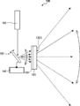
- FIG. 1 shows the basic configuration of the optical scanning apparatus according to the first embodiment of the present invention.
- the optical scanning apparatus is composed of a light source 151 made of a semiconductor laser, a diffraction element 161 composed of a support 131 and a liquid crystal diffraction element 121 arranged on at least one surface of the support 131, and a light source. It is provided with an optical deflector 101 that deflects the emitted light source.
- the diffraction element 161 and the light deflector 101 correspond to the light deflector in the present invention.
- the liquid crystal diffraction element 121 corresponds to the optically anisotropic layer in the present invention.
- FIG. 1 is an example of an optical scanning device that uses a MEMS (Micro Electro Mechanical Systems) optical deflector as the optical deflector 101.
- MEMS Micro Electro Mechanical Systems
- the liquid crystal diffusing element 121 is a cured layer of the liquid crystal composition, the optical axis of the liquid crystal compound contained in the liquid crystal composition is parallel to the main surface of the liquid crystal diffusing element, and the liquid crystal diffusing element is in the plane thereof. It is a liquid crystal alignment pattern arranged along at least one direction, and has a liquid crystal alignment pattern in which the orientation of the optical axis of the liquid crystal compound is continuously changed by rotation.
- the liquid crystal diffraction element diffracts the incident light by having a liquid crystal orientation pattern.
- the diffraction angle of light by the liquid crystal diffraction element is the length of one cycle p in which the direction of the optical axis of the liquid crystal compound is rotated by 180 ° in the liquid crystal alignment pattern (hereinafter, also simply referred to as “one cycle p”).
- one cycle p the longer the period p, the larger the diffraction angle.
- the laser beam emitted from the light source 151 is deflected in the direction of the diffraction element 161 by the optical deflector 101.
- the deflected light enters any place of the diffraction element 161 and is diffracted in a desired direction such as by expanding the deflection angle of the light by the diffraction element 161 to function as the optical scanning device 100.
- the optical deflector 101 controls the deflection angle incident on the diffraction element by the controller 141.
- a reflection mirror, a condenser lens, a deflector, a retardation plate, etc. may be appropriately inserted in the optical path.
- the optical scanning device 100 deflects the light emitted by the light source 151 by an optical deflector 101 at a predetermined angle.
- the polarization angle by the optical deflector 101 is appropriately changed by the controller 141, the traveling direction of the light is changed, and scanning using the light is performed.
- the light deflected by the light deflector 101 is diffracted by the diffraction element 161 to expand the deflection angle as shown in the illustrated example. Therefore, the scanning range is expanded.
- the wavelength of the laser beam mainly used as a light source has a temperature dependence, and generally has a characteristic that the oscillation wavelength shifts to the long wavelength side due to a temperature rise.
- the degree of change is about +8 nm with an increase of 40 ° C. That is, when a 940 nm laser is used and the temperature of the light source rises by 40 ° C., the oscillation wavelength of the light source becomes about 948 nm.
- the diffraction angle by the diffraction element changes depending on the wavelength of light.
- the diffraction angle of light by the liquid crystal diffraction element depends on one cycle p of the liquid crystal alignment pattern. Therefore, when the liquid crystal diffraction element expands in the plane direction due to the temperature rise, one cycle p becomes longer and the diffraction angle becomes smaller. Therefore, it is conceivable that the increase in the deflection angle due to the increase in the oscillation wavelength of the light source is offset by the decrease in the diffraction angle due to the expansion of the liquid crystal diffraction element to make the deflection angle constant regardless of the temperature.
- the liquid crystal diffraction element is formed by polymerizing a liquid crystal compound, and its thickness is several microns to several tens of microns.
- a support having a liquid crystal diffraction element on at least one surface has a size of several hundred microns or more, and has a higher elastic modulus than a liquid crystal diffraction element obtained by polymerizing a liquid crystal compound. Therefore, when the liquid crystal diffraction element and the support expand and contract with the temperature fluctuation, the expansion and contraction of the liquid crystal diffraction element is regulated by the support, and the state of the liquid crystal diffraction element is mainly controlled by the expansion and contraction of the support. ..
- the diffraction angle of the diffraction element due to the temperature fluctuation is mainly controlled by the thermal characteristics of the support that the liquid crystal diffraction element follows, not the thermal characteristics of the liquid crystal diffraction element itself.
- the coefficient of linear expansion of the support is related to the following conditional expression (1), the influence of the wavelength increment of the light source can be suppressed.
- This conditional expression (1) stipulates that the deviation of the scanning angle is less than 0.3 °.
- the support satisfies this conditional expression (1), the scanning angle deviation due to temperature fluctuation can be reduced.
- the scanning angle deviation will be described by giving specific numerical values.
- the linear expansion coefficient of the support is small, for example, when it is zero, the emission angle with respect to the incident angle of 30 °. Is changed from 60 ° to 60.4 °, and the scanning angle deviation is 0.4 °.
- the coefficient of linear expansion of the support is zero, the left side of the conditional expression (1) is about 2.1 ⁇ 10 -4 , which does not satisfy the conditional expression (1).
- the scanning angle deviation is 0.3 ° or less, and when the coefficient of linear expansion is 100 ppm / ° C, the scanning angle deviation is 0.2 ° or less.
- the scanning angle deviation is approximately 0. This makes it possible to realize an optical scanning device that is resistant to temperature fluctuations.
- the coefficient of linear expansion of the support is 50 ppm / ° C.
- the left side of the conditional expression (1) is about 1.6 ⁇ 10 -4 , which satisfies the conditional expression (1).
- the left side of the conditional expression (1) is about 1.1 ⁇ 10 -4 , which satisfies the conditional expression (1).
- the coefficient of linear expansion of the support is 200 ppm / ° C.
- the left side of the conditional expression (1) is about 0.1 ⁇ 10 -4 , which satisfies the conditional expression (1).
- the configuration is such that the MEMS optical deflector is provided as the optical deflector 101, but the present invention is not limited to this, and the optical deflector 101 deflects the incident light by a predetermined angle and deflects the incident light. Anything that can change the angle will do.
- a liquid crystal optical phase modulation element is provided as the optical deflector 101.
- the optical scanning device 100 includes a light source (not shown) arranged on the left side of the optical deflector 101 in the figure, an optical deflector 101, a diffraction element 161 and a controller 141.
- the liquid crystal optical phase modulation element controls the deflection direction of incident light by applying a voltage to the liquid crystal layer to control the orientation of the liquid crystal in the liquid crystal layer.
- FIG. 3 is a conceptual diagram for explaining the operation of the optical scanning device 100 shown in FIG.
- the liquid crystal optical phase modulation element 101 deflects the light emitted from a light source (not shown) by a predetermined angle (see the solid arrow).
- the polarization angle of the liquid crystal optical phase modulation element 101 is changed by the controller 141. That is, as shown by the arrow of the broken line in FIG. 3, the polarization angle by the liquid crystal optical phase modulation element 101 is appropriately changed by the controller 141 to change the traveling direction of the light. As a result, the traveling direction of the light is changed, and the optical scanning device 100 performs scanning using the light.
- the light deflected by the light deflector 101 is diffracted by the diffraction element 161 to expand the deflection angle as shown in the illustrated example. Therefore, the scanning range is expanded.
- the liquid crystal diffraction element 120 of the diffraction element 161 has a region (120a to 120e) in which one cycle of the liquid crystal alignment pattern is different in the plane.
- the smaller one cycle of the liquid crystal alignment pattern the larger the diffraction angle.
- the diffraction angle of the liquid crystal diffraction element 120 is gradually increased from the center of the deflection by the optical deflector 101 toward the outside (both ends). .. This means that, in FIG.
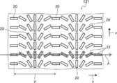
- FIG. 4 conceptually shows an example of the diffraction element 161.
- FIG. 4 is a view of the diffraction grating 161 viewed in the same direction as FIGS. 1 to 3, and is a side view of the diffraction grating 161.
- the diffraction element 161 is in the form of a sheet, and has a support 131, an alignment film 13, and an optically anisotropic layer (liquid crystal diffraction element) 121.
- the liquid crystal diffraction element 121 further deflects the light deflected by the optical deflector 101 by diffracting the light deflected by the optical deflector 101 in the deflection direction by the optical deflector 101.
- the sheet surface direction of the liquid crystal diffraction element 121 is defined as the xy direction, and the thickness direction is defined as the z direction. In FIG.
- the horizontal direction in the figure is the direction in which the optic axis derived from the liquid crystal compound rotates in one direction (axis A direction described later), and this direction is defined as the x direction. Therefore, the y direction is a direction orthogonal to the paper surface of FIG.
- the liquid crystal diffraction element 121 is planar, but the liquid crystal diffraction element 121 is not limited to a planar shape and may be a curved surface.
- ⁇ Support> As the support 131, various sheet-like materials (films, plate-like materials) can be used as long as the coefficient of thermal expansion satisfies a predetermined condition and the alignment film and the optically anisotropic layer can be supported.
- a transparent support is preferable, and examples thereof include a polyacrylic resin film such as polymethylmethacrylate, a cellulosic resin film such as cellulose triacetate, and a cycloolefin polymer film.
- the cycloolefin polymer-based film include the trade name "Arton” manufactured by JSR Corporation and the trade name "Zeonoa” manufactured by Zeon Corporation.
- the coefficient of linear expansion is a constant peculiar to the material, and the value of the coefficient of linear expansion can be adjusted as a composite material by mixing a plurality of materials or forming a laminated structure.
- the support 131 has anisotropy in the thermal expansion direction, it is desirable that the support 131 be parallel or perpendicular to the periodic direction of the diffraction element.
- the linear expansion coefficient may be high in the stretching direction. In that case, it is desirable that the stretching direction and the periodic direction of the diffraction element be parallel. In the opposite case, it is desirable that the stretching direction and the periodic direction of the diffraction element are orthogonal to each other.
- an alignment film 13 is formed on the surface of the support 131.
- the alignment film 13 is an alignment film for orienting the liquid crystal compound 20 in a predetermined liquid crystal alignment pattern when forming the optically anisotropic layer 121.
- the optically anisotropic layer 121 changes the orientation of the optical axis 22 derived from the liquid crystal compound 20 while continuously rotating along one direction in the plane. Has a pattern. Therefore, the alignment film 13 is formed so that the optically anisotropic layer 121 can form this liquid crystal alignment pattern.
- the direction of the optical axis 22 rotates 180 ° in one direction (direction along the axis A described later) in which the direction of the optical axis 22 changes while continuously rotating in the liquid crystal alignment pattern.
- the length to be used is one cycle (rotation cycle p of the optic axis 22).
- one cycle of the optically anisotropic layer 121 is gradually shortened from the center of the deflection (deflection direction (deflection direction)) by the optical deflector 101 toward the outside. Further, the rotation direction of the optical axis of the liquid crystal compound 20 is reversed at the center of deflection by the optical deflector 101 in the direction along the axis A (arrow x direction). Therefore, the alignment film 13 is formed so that the optically anisotropic layer 121 can form this liquid crystal alignment pattern.
- the alignment film 13 various known ones can be used.
- the alignment film 13 include a rubbing-treated film made of an organic compound such as a polymer, an oblique vapor-deposited film of an inorganic compound, a film having microgrooves, and ⁇ -tricosanoic acid, dioctadecylmethylammonium chloride, and methyl stearylate.
- Examples thereof include a membrane obtained by accumulating LB (Langmuir-Blodgett) membranes obtained by the Langmuir-Blodget method of organic compounds.
- Examples of the alignment film 13 include those formed by rubbing the surface of the polymer layer. The rubbing treatment is carried out by rubbing the surface of the polymer layer with paper or cloth several times in a certain direction.
- the types of polymers used for the alignment film are polyimide, polyvinyl alcohol, polymers having a polymerizable group described in JP-A-9-152509, JP-A-2005-97377, JP-A-2005-99228, and JP-A-2005-99228.
- the alignment film described in JP-A-2005-128503 can be preferably used.
- the orthogonal alignment film referred to in the present invention means an alignment film in which the major axis of the molecule of the polymerizable rod-shaped liquid crystal compound is oriented so as to be substantially orthogonal to the rubbing direction of the orthogonal alignment film.
- the thickness of the alignment film does not have to be thick as long as it can provide the alignment function, and is preferably 0.01 to 5 ⁇ m, more preferably 0.05 to 2 ⁇ m.
- a so-called photo-alignment film in which a photo-alignable material is irradiated with polarized light or non-polarized light to form an alignment film can also be used. That is, a light alignment material may be applied onto the support 131 to form a photoalignment film.
- Polarized light irradiation can be performed from a vertical direction or an oblique direction with respect to the photoalignment film, and non-polarized light irradiation can be performed from an oblique direction with respect to the photoalignment film.
- Examples of the photoalignment material used for the photoalignment film that can be used in the present invention include JP-A-2006-285197, JP-A-2007-76839, JP-A-2007-138138, and JP-A-2007-94071.
- JP-A-9-118717 JP-A-10-506420, JP-A-2003-505561, WO2010 / 150748, JP-A-2013-177561, and JP-A-2014.
- Preferred examples thereof include photodimerizable compounds described in JP-A-12823, particularly cinnamate compounds, chalcone compounds and coumarin compounds.
- Particularly preferred are azo compounds, photocrosslinkable polyimides, polyamides, esters, cinnamate compounds, and chalcone compounds.
- FIG. 8 shows a schematic view of an alignment film exposure apparatus in which the photoalignment material is applied onto the support 131 and dried, and then the alignment film is exposed to form an alignment pattern.
- the exposure apparatus 50 is arranged on the light path 54 of the light source 54 provided with the laser 52, the polarization beam splitter 56 that separates the laser beam 70 from the laser 52 into two, and the two separated rays 72A and 72B, respectively.
- Mirrors 58A, 58B and ⁇ / 4 plates 60A, 60B are provided.
- the light source 54 emits linearly polarized light P 0 .
- lambda / 4 plate 60A is linearly polarized light P 0 on the right circularly polarized light P R
- lambda / 4 plate 60B converts the linearly polarized light P 0 to the left circularly polarized light P L.
- a support 131 having an alignment film 13 before the alignment pattern is formed is arranged in the exposed portion, and two light rays 72A and 72B are crossed and interfered with each other on the alignment film 13, and the interference light is transmitted to the alignment film 13. Irradiate and expose. Due to the interference at this time, the polarization state of the light applied to the alignment film 13 changes periodically in the form of interference fringes. As a result, an orientation pattern in which the orientation state changes periodically can be obtained. In the exposure apparatus 50, the period of the orientation pattern can be changed by changing the intersection angle ⁇ of the two rays 72A and 72B.
- the optic axis 22 rotates in one direction.
- the optically anisotropic layer 121 which will be described later, on the alignment film 13 having the alignment pattern in which the orientation state changes periodically in this way, the optical anisotropy provided with the liquid crystal alignment pattern corresponding to this period.
- Layer 121 can be formed.
- the rotation direction of the optical shaft 22 can be reversed by rotating the optical axes of the ⁇ / 4 plate 60A and the ⁇ / 4 plate 60B by 90 °, respectively.
- the exposure apparatus 80 shown in FIG. 9 is an exposure apparatus that is also used when forming a concentric liquid crystal alignment pattern as shown in FIG. 7.
- the exposure apparatus 80 includes a light source 84 provided with a laser 82, a polarization beam splitter 86 that splits the laser beam M from the laser 82 into S-polarized light MS and P-polarized light MP, and a mirror 90A arranged in the optical path of the P-polarized light MP.
- the P-polarized MP divided by the polarizing beam splitter 86 is reflected by the mirror 90A and incident on the polarizing beam splitter 94.
- the S-polarized light MS split by the polarizing beam splitter 86 is reflected by the mirror 90B, focused by the lens 92, and incident on the polarizing beam splitter 94.
- the P-polarized MP and the S-polarized MS are combined by a polarizing beam splitter 94 and become right-circularly polarized light and left-handed circularly polarized light according to the polarization direction by the ⁇ / 4 plate 96, and the alignment film 13 on the support 131. It is incident on.
- the polarization state of the light applied to the alignment film 13 periodically changes in an interference fringe pattern. Since the intersection angle of the left-handed circularly polarized light and the right-handed circularly polarized light changes from the inside to the outside of the concentric circles, an exposure pattern in which the pitch changes from the inside to the outside can be obtained. As a result, in the alignment film 13, a concentric alignment pattern in which the alignment state changes periodically can be obtained.
- the length of one cycle (rotation cycle p) in which the optical axis 22 of the liquid crystal compound 20 continuously rotates 180 ° along one direction is the refractive power of the lens 92 (F number of the lens 92). It can be controlled by changing the focal length of the lens 92, the distance between the lens 92 and the alignment film 13, and the like.
- the length of one cycle in which the optic axis 22 rotates 180 ° in one direction in which the optic axis 22 continuously rotates can be changed.
- the length of one cycle in which the optic axis 22 rotates 180 ° can be changed depending on the degree of focusing of the light transmitted through the lens 92 that interferes with the parallel light. More specifically, when the refractive power of the lens 92 is weakened, it approaches parallel light, so that the length of one cycle in which the optic axis 22 rotates 180 ° gradually shortens from the inside to the outside, and the F number becomes growing.
- the refractive power of the lens 92 is increased, the length of one cycle in which the optical axis 22 rotates by 180 ° suddenly shortens from the inside to the outside, and the F number becomes small.
- the configuration in which one cycle (rotation cycle p) in which the optic axis 22 rotates 180 ° in one direction in which the optic axis 22 continuously rotates is changed, the liquid crystal compound 20 is formed in only one direction in the direction of arrow X. It can also be used in a configuration in which the optical shaft 22 continuously rotates and changes. For example, by gradually shortening one cycle in which the optical axis 22 rotates by 180 ° in the direction of the arrow X, an optical element that transmits light so as to be focused can be obtained.
- liquid crystal alignment pattern by reversing the direction in which the optical axis 22 rotates by 180 °, it is possible to obtain an optical element that transmits light so as to diffuse only in the direction of arrow X. By reversing the turning direction of the incident circularly polarized light, it is possible to obtain an optical element that transmits light so as to diffuse only in the X direction of the arrow.
- one cycle in which the optical axis 22 rotates 180 ° in the arrow X direction is not gradually changed depending on the application of the optical element, but in the arrow X direction. It is also possible to use a configuration in which the optical axis 22 is partially rotated by 180 ° and has regions having different cycles. For example, as a method of partially changing one cycle in which the optic axis 22 rotates 180 °, a method of scanning and exposing a photoalignment film and patterning while arbitrarily changing the polarization direction of the focused laser light is used. be able to.
- the alignment film 13 is provided as a preferable embodiment, and is not an indispensable constituent requirement.
- the optically anisotropic layer 121 is derived from the liquid crystal compound 20 by forming an orientation pattern on the support 131 by a method of rubbing the support 131, a method of processing the support 131 with a laser beam, or the like. It is also possible to have a configuration having a liquid crystal orientation pattern in which the orientation of the optical axis 22 is changing while continuously rotating along at least one direction in the plane.
- an optically anisotropic layer (liquid crystal diffraction element) 121 which is a cured layer of the liquid crystal composition containing the liquid crystal compound 20, is provided on the surface of the alignment film 13.
- the optical axes (slow-phase axes) of the liquid crystal compound are liquid crystal patterns arranged along at least one direction in the plane of the optically anisotropic layer, and the optics of the liquid crystal compound 20
- the axis 22 has a liquid crystal orientation pattern in which the orientation changes in one direction.
- the retardation R is preferably 0.4 ⁇ to 0.6 ⁇ , more preferably 0.45 ⁇ to 0.55 ⁇ , and particularly preferably 0.5 ⁇ .
- ⁇ n is the birefringence of the optically anisotropic layer 121
- d1 is the thickness.
- the liquid crystal diffraction element 121 functions as a transmission type diffraction grating.
- the principle of functioning as a diffraction grating will be described with reference to FIGS. 4 to 6.
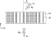
- FIG. 5 is a schematic plan view of the optically anisotropic layer 121, that is, FIG. 4 is a view of FIG. 4 viewed from above in the drawing.
- the liquid crystal compound 20 is immobilized in a liquid crystal orientation pattern in which the optical axis 22 is continuously rotated in one direction.
- the optic axis 22 continuously changes in rotation in the direction along the axis A in FIG. 5, which coincides with the arrow x direction. That is, the liquid crystal compound 20 is oriented so that the angle formed by the in-plane component of the long axis (axis of abnormal light: director) of the liquid crystal compound 20 defined as the optical axis 22 and the axis A changes in rotation. ..
- FIG. As shown in FIG.
- the direction of the optical axis 22 of the liquid crystal compound 20 coincides with that of the liquid crystal compound 20 arranged in the direction orthogonal to the axis A, that is, in the direction of the arrow y.
- the optically anisotropic layer 121 exhibits the function as a general ⁇ / 2 plate as described above for each region where the directions of the optical axes 22 of the liquid crystal compound 20 in the y direction coincide with each other.
- the angle formed by the optical axis 22 and the axis A of the liquid crystal compound 20 arranged along the axis A differs depending on the position in the axis A direction. It is a pattern oriented and fixed so that the angle formed by the optic axis 22 and the axis A gradually changes from ⁇ to ⁇ + 180 ° or ⁇ -180 ° along the axis A.
- the optical axis 22 of the liquid crystal compound 20 is parallel to the plane of the optically anisotropic layer 121, and the direction of the optical axis 22 is constant.
- a local region that is, a region in which the liquid crystal compound 20 is arranged in the y direction of the arrow is arranged in the x direction orthogonal to the y direction of the arrow, and is arranged among a plurality of local regions arranged in the x direction of the arrow.
- a liquid crystal alignment pattern in which the direction of the optical axis 22 is continuously rotationally changed in one direction (direction along the axis A) is referred to as horizontal rotational orientation.
- the angle change of the optic axis 22 toward the axis A direction may be a thing that rotates at a non-uniform angle interval instead of a constant angle interval.
- the average value of the orientation of the optical axis 22 in the unit region changes linearly at a constant rate, it means that the value gradually changes.
- the change in the inclination of the optical axis between the unit regions adjacent to the axis A direction in which the optical axes 22 have different inclinations is preferably 45 ° or less. It is preferable that the change in the slope of the adjacent unit region is smaller.
- the distance at which the angle formed by the optical axis 22 and the axis A changes from ⁇ to ⁇ + 180 ° (returns to the original) toward the axis A direction that is, the period during which the optical axis 22 rotates 180 °.
- the rotation cycle (1 cycle) p is preferably 0.1 to 5 ⁇ m. The shorter the rotation period p, the larger the diffraction angle by the optically anisotropic layer 121, that is, the liquid crystal diffraction element 121. Therefore, the rotation period p may be determined according to the wavelength of the incident light on the liquid crystal diffraction element 121 and the desired emission angle.
- the diffraction element 161 gives a phase difference of ⁇ / 2 with respect to the incident light, and emits the incident light incident at an incident angle of 0 °, that is, the vertically incident incident light at an emission angle ⁇ . Emit with 2. That is, as shown in FIG. 6, the optical when the perpendicular plane of the anisotropic layer 121 with light L 1 of the right circularly polarized light P R is incident, left circular polarization P L in the direction forming an normal direction and the angle theta 2 Light L 2 is emitted.
- injecting light perpendicularly to the surface of the optically anisotropic layer 121 means, in other words, injecting light along the normal of the surface.
- injecting light perpendicularly to the surface of the optically anisotropic layer 121 means, in other words, injecting light along the normal of the surface.
- incident light L 1 light L 1 of the right circularly polarized light P R that is incident on the optically anisotropic layer 121.
- emitted light L 2 light L 2 of the left-handed circularly polarized light P L emitted from the optical anisotropic layer.
- the exit angle of the outgoing light L 2 is the angle formed by the normal direction of the optically anisotropic layer 121 and the outgoing light L 2 is.
- the diffraction direction of the light L 2 emitted from the liquid crystal diffraction element 121 is the circularly polarized light of the light incident on the liquid crystal diffraction element 121.
- the state is controlled to cause incident. That is, as shown in the illustrated example, when the incident light is linearly polarized light, the direction of diffraction of the light is either by inserting a ⁇ / 4 plate, converting it to circularly polarized light on either the left or right side, and then incident light. Can only be.
- the wavelength ⁇ of the light that causes the diffraction action by the liquid crystal diffraction element (optically anisotropic layer) 121 may be from ultraviolet to visible light, infrared light, or even an electromagnetic wave level.
- the liquid crystal compound 20 a rod-shaped liquid crystal compound and a disk-shaped liquid crystal compound can be used.
- the rotation cycle may be designed so that a desired diffraction angle ⁇ 2 can be obtained so as to satisfy the above equation (1) in consideration of the incident angle ⁇ 1.
- the light deflected by the optical deflector 101 is diffracted by the diffraction element 161 (optical anisotropic layer 121), so that the maximum deflection angle ⁇ of the optical deflector 101 is ⁇ . It enables the deflection of light by the deflection angle of the maximum emission angle ⁇ max out, which is much larger than max.
- the diffraction angle of light by the optically anisotropic layer 121 increases as one cycle in which the optical axis 22 of the liquid crystal compound 20 rotates by 180 °, that is, the rotation cycle p is shorter.
- the deflection direction (swirl direction) of the incident circular polarization is the same, the diffraction direction of the light by the optically anisotropic layer 121 is opposite depending on the rotation direction of the optical axis 22 of the liquid crystal compound 20. That is, when the incident light L 1 is a right circularly polarized light P R, as viewed from the exit surface side, the rotational direction of the optical axis 22, in the axial direction A (direction of arrow x) as shown in FIGS. 4 to 6 When clockwise, the emitted light L 2 is diffracted, for example, in the axis A direction.
- the incident light L 1 is a right circularly polarized light P R, as viewed from the exit side, when the rotation direction of the optical axis 22 is a counterclockwise toward the axis A direction, The emitted light L 2 is diffracted in the direction opposite to the axis A direction (direction of the arrow).
- the optically anisotropic layer 121 deflects the rotation period p of the optical axis 22 of the liquid crystal compound 20 toward the axis A direction by the optical deflector 101 (deflection direction). ) Gradually shorten from the center to the outside. That is, the diffraction angle of light by the optically anisotropic layer 121 increases toward the outside in the deflection direction.
- the optically anisotropic layer 121 reverses the rotation direction of the optical axis 22 of the liquid crystal compound 20 toward the axis A direction at the center of deflection by the optical deflector 101. ..
- the rotation direction of the optical axis 22 toward the axis A direction is counterclockwise from the upstream side in the axis A direction to the center in the deflection direction toward the axis A direction, and the center of deflection.
- the rotation direction of the optical shaft 22 is reversed, and the rotation direction of the optical shaft 22 toward the axis A direction is clockwise from the center of deflection toward the downstream in the axis A direction.
- the rotation direction of the optical axis 22 is usually reversed at the center of the optically anisotropic layer 121 in the axis A direction (arrow x direction), that is, in one direction in which the optical axis 22 rotates. That is, in the optical scanning apparatus 100, the center of deflection in the optical deflector 101 is usually aligned with the center of the optically anisotropic layer 121 in the axis A direction.
- the rotation period p may be continuously shortened from the center of deflection toward the outside, or may be gradually shortened.
- the optically anisotropic layer 121 is formed, for example, by a liquid crystal composition containing a liquid crystal compound.
- the liquid crystal composition containing the liquid crystal compound for forming the optically anisotropic layer 121 contains other components such as a leveling agent, an orientation control agent, a polymerization initiator and an orientation aid in addition to the liquid crystal compound. You may.
- the optically anisotropic layer 121 is composed of a cured layer of a liquid crystal composition containing a rod-shaped liquid crystal compound or a disk-shaped liquid crystal compound, and the optical axis of the rod-shaped liquid crystal compound or the optical axis of the disk-shaped liquid crystal compound is oriented as described above. It has a liquid crystal orientation pattern.
- the present invention includes an embodiment in which a laminate integrally provided with a support 131 and an alignment film functions as a ⁇ / 2 plate.
- the liquid crystal composition for forming the optically anisotropic layer contains a rod-shaped liquid crystal compound or a disk-shaped liquid crystal compound, and further contains other components such as a leveling agent, an orientation control agent, a polymerization initiator, and an orientation aid. May be contained.
- the optically anisotropic layer preferably has a wide band with respect to the wavelength of the incident light, and is preferably formed by using a liquid crystal material having a birefringence of inverse dispersion. Further, it is also preferable to impart a twisting component to the liquid crystal composition and to laminate different retardation layers so that the optically anisotropic layer has a substantially wide band with respect to the wavelength of the incident light.
- a method of realizing a wide-band patterned ⁇ / 2 plate by laminating two layers of liquid crystals having different twist directions is shown in Japanese Patent Application Laid-Open No. 2014-089476 and the like. , Can be preferably used in the present invention.
- rod-shaped liquid crystal compound examples include azomethines, azoxys, cyanobiphenyls, cyanophenyl esters, benzoic acid esters, cyclohexanecarboxylic acid phenyl esters, cyanophenylcyclohexanes, cyano-substituted phenylpyrimidines, alkoxy-substituted phenylpyrimidines, and the like. Phenyldioxans, trans, and alkenylcyclohexylbenzonitriles are preferably used. Not only low molecular weight liquid crystal molecules as described above, but also high molecular weight liquid crystal molecules can be used.
- the polymerizable rod-shaped liquid crystal compound examples include Makromol. Chem., 190, 2255 (1989), Advanced Materials 5, 107 (1993).
- US Pat. Nos. 4,683,327, 562,648, 5770107, International Publication 95/22586, 95/24455, 97/00600, 98/23580, 98/52905 , JP-A No. 1-272551, No. 6-16616, No. 7-110469, No. 11-8801, and Japanese Patent Application No. 2001-64627 can be used.
- the rod-shaped liquid crystal compound for example, those described in JP-A No. 11-513019 and JP-A-2007-279688 can also be preferably used.
- the disk-shaped liquid crystal compound for example, those described in JP-A-2007-108732 and JP-A-2010-244038 can be preferably used.
- the liquid crystal compound 20 rises in the thickness direction in the optically anisotropic layer, and the optical axis 22 derived from the liquid crystal compound has a disk surface. It is defined as the axis perpendicular to, the so-called phase-advancing axis.
- the optically anisotropic layer 121 can be formed by coating a liquid crystal composition on the alignment film 13 in multiple layers.
- a liquid crystal composition is applied on an alignment film, heated, cooled, and then cured by ultraviolet rays to prepare a first liquid crystal immobilization layer, and then the second and subsequent layers are fixed to the liquid crystal. It refers to repeating the process of overcoating the liquid crystal layer, applying it, heating it in the same manner, cooling it, and then curing it with ultraviolet rays.
- the optically anisotropic layer 121 by coating the layers as described above, even when the total thickness of the optically anisotropic layer 121 is increased, the orientation direction of the alignment film 13 can be changed to the optically anisotropic layer 121. It can be reflected from the lower surface to the upper surface of.
- FIG. 7 is a schematic plan view of the optically anisotropic layer in the design modification example of the liquid crystal diffraction element.
- the liquid crystal alignment pattern in the optically anisotropic layer 122 shown in FIG. 7 is different from the liquid crystal alignment pattern in the optically anisotropic layer 121 described above. In FIG. 7, only the optical axis 22 is shown.
- the optically anisotropic layer 122 of FIG. 7 is a liquid crystal in which the direction of the optical axis 22 gradually rotates and changes along multiple directions from the center side to the outside, for example, axes A 1 , A 2 , A 3, and so on. It has an orientation pattern. That is, the liquid crystal alignment pattern of the optically anisotropic layer 122 shown in FIG.
- the liquid crystal alignment pattern of the optically anisotropic layer 122 shown in FIG. 7 is a concentric pattern having one direction in which the direction of the optical axis changes while continuously rotating, in a concentric pattern from the inside to the outside. Is. Due to the liquid crystal alignment pattern shown in FIG. 7, the absolute phase of the incident light changes by a different amount of change between the local regions in which the directions of the optical axes 22 are different. If a liquid crystal orientation pattern in which the optical axis rotates in a radial manner as shown in FIG. 7 is provided, the incident light can be transmitted as divergent light or condensed light. That is, the function as a concave lens or a convex lens can be realized by the liquid crystal alignment pattern in the optically anisotropic layer 121.
- the function of the concave lens of the optically anisotropic layer 122 shown in FIG. 7 is used for the diffraction element 161.
- the maximum deflection angle ⁇ max emitted from the optical deflector 101 can be spread most efficiently.
- the value is finite to the extent that there is no practical problem depending on the beam diameter of the laser beam to be irradiated. May be good. For example, it may be about 10 to several hundred ⁇ m.
- the liquid crystal compound of the liquid crystal diffraction element is oriented in one direction in the thickness direction, but the present invention is not limited to this.
- the optically anisotropic layer constituting the liquid crystal diffraction element may have a liquid crystal compound twisted or oriented along a spiral axis extending along the thickness direction. Further, a plurality of liquid crystal layers having different twist orientation directions may be laminated. In this case, the tolerance for the incident angle and wavelength of light is widened.
- a diffraction element 162 having an optically anisotropic layer 122 functioning as a concave lens and an optical deflector that deflects light radially as an optical deflector A vessel 102 is used.
- the light deflector 102 deflects light at, for example, an orientation of 360 ° and a polar angle of 0 to 35 °.
- the optical scanning device may preferably include a condenser lens 110 as a condenser element, a ⁇ / 4 plate 111, and a condenser lens 112.
- the condensing lens 110 is a known condensing lens that slightly condenses the light incident on the liquid crystal diffraction element. By having the condenser lens 110, the light (light beam) emitted from the optical scanning device 100 (liquid crystal diffraction element 122) can be made into appropriate parallel light, and the straightness can be improved.
- a MEMS optical deflector described in Japanese Patent Application Laid-Open No. 2012-208352, Japanese Patent Application Laid-Open No. 2014- Light is emitted by swinging a mirror using a piezoelectric actuator or the like, such as the MEMS optical deflector described in Japanese Patent Application Laid-Open No. 134642 and the MEMS optical deflector described in Japanese Patent Application Laid-Open No. 2015-22064.
- the optical scanning apparatus of the present invention has a simple structure, a simple drive, and a large angle deflection, it can be applied to all applications for scanning light for which light weight and miniaturization are desired.
- a drawing device using a beam scan, a beam scan type projection display, a beam scan type head-up display, a beam scan type AR glass, and the like In this case, it can be applied as a device that deflects light in a wide wavelength range including visible light.
- the optical deflector is not limited to the above-mentioned MEMS optical deflector and liquid crystal optical phase modulator, and is a galvano mirror, a polygon mirror, and an optical phased array deflector (optical phase modulator). ) Etc., various known light deflectors can be used. Among them, the MEMS optical deflection element and the optical phased array deflection element described above are preferably used as the optical deflector in that the mechanical movable portion is small and the mechanical movable portion is small.
- Coating liquid for forming an alignment film ⁇ Material for photo-alignment A 1.00 parts by mass Water 16.00 parts by mass Butoxyethanol 42.00 parts by mass Propylene glycol monomethyl ether 42.00 parts by mass ⁇ ⁇
- the alignment film was exposed using the exposure apparatus shown in FIG. 9 to form an alignment film P-1 having an alignment pattern.
- a laser that emits laser light having a wavelength (405 nm) was used.
- the exposure amount due to the interference light was set to 100 mJ / cm 2 .
- the refractive power of the lens (convex lens) is adjusted and the optically anisotropic layer is formed thereafter, the period of rotation of the optical axis of the liquid crystal compound in the optically anisotropic layer gradually increases from the center to the outside. , I tried to shorten it.
- composition A-1 was prepared as a liquid crystal composition for forming an optically anisotropic layer.
- Composition A-1 Liquid Crystal Compound L-1 100.00 parts by mass Polymerization initiator (BASF, Irgacure (registered trademark) 907) 3.00 parts by mass Photosensitizer (manufactured by Nippon Kayaku Co., Ltd., KAYACURE DETX-S) 1.00 parts by mass Leveling agent T-1 0.08 parts by mass Methyl ethyl ketone 313.0 parts by mass ⁇ ⁇
- the optically anisotropic layer was formed by coating the composition A-1 on the alignment film P-1 in multiple layers.
- multi-layer coating first, the composition A-1 of the first layer is coated on the alignment film, heated, cooled, and then cured by ultraviolet rays to prepare a liquid crystal-immobilized layer, and then the second and subsequent layers are immobilized with the liquid crystal. It refers to repeating the process of overcoating the layers, applying them, and then heating and cooling them in the same way, followed by UV curing.
- the orientation direction of the alignment film is reflected from the lower surface to the upper surface of the optically anisotropic layer even when the total thickness of the optically anisotropic layer is increased.
- the composition A-1 is applied on the alignment film P-1, the coating film is heated to 70 ° C. on a hot plate, then cooled to 25 ° C., and then pressed under a nitrogen atmosphere.
- the orientation of the liquid crystal compound was fixed by irradiating the coating film with an ultraviolet ray having a wavelength of 365 nm using a mercury lamp at an irradiation amount of 100 mJ / cm 2.
- the film thickness of the first liquid crystal immobilization layer was 0.2 ⁇ m.
- the second and subsequent layers were overcoated on the liquid crystal immobilization layer, heated under the same conditions as above, cooled, and then cured by ultraviolet rays to prepare a liquid crystal immobilization layer.
- the diffraction element having the support, the alignment film, and the optically anisotropic layer by repeatedly coating the grating until the total thickness reaches a desired film thickness to form the optically anisotropic layer.
- the optically anisotropic layer finally has a liquid crystal ⁇ n 940 ⁇ thickness (Re (940)) of 470 nm, and is optically anisotropic from the center to the outside in one direction in which the optic axis rotates.
- the rotation cycle of the optical axis of the liquid crystal compound in the layer was gradually shortened and that the rotation direction of the optical axis was reversed at the center.
- the rotation cycle (1 cycle) in which the optical axis of the liquid crystal compound rotates by 180 ° has a very large rotation cycle in the central portion (the inverse number of the rotation cycle is 0).
- the rotation cycle at a distance of 2.5 mm from the center is 10.6 ⁇ m
- the rotation cycle at a distance of 5.0 mm from the center is 5.3 ⁇ m
- the rotation cycle gradually shortens from the center to the outside. It was a liquid crystal orientation pattern.
- a 940 nm semiconductor laser was prepared as the light source laser. Further, a ⁇ / 4 plate (circular polarizing plate, Edmund) was prepared in order to convert the linearly polarized light of the laser into circularly polarized light and incident it on the liquid crystal diffraction element. ⁇ n 940 ⁇ d (Re (940)) was 470 nm. Further, a micromirror device was produced by the method described in Japanese Patent Application Laid-Open No. 2014-134642. The diameter of the mirror portion was 4 mm, and the deflection angle was ⁇ 35 °. These were configured as shown in FIG. 1 to produce an optical scanning device.
- the polarization direction of the laser beam and the in-plane slow-phase axis of the ⁇ / 4 plate were intersected at 45 ° so that they were converted into circularly polarized light.
- a condenser lens (convex lens) is arranged between the light source and the light deflector.
- the characteristic values of each optical component are as follows. The light diameter of the laser beam was 3 mm, the focal length of the condenser lens was 35 mm, the distance between the condenser lens and the MEMS was 16 mm, and the distance between the MEMS and the liquid crystal diffractometer was 7 mm.
- the range of the deflection angle of the emitted light by MEMS was ⁇ 35 °.
- the diameter of the liquid crystal diffraction element is 20 mm.
- the liquid crystal diffractometer has a very large rotation cycle at the center (the reciprocal of the rotation cycle is 0), the rotation cycle at a position with a radius of 5 mm is 4.8 ⁇ m, and the rotation cycle at a position with a radius of 10 mm is 2.6 ⁇ m.
- the center wavelength ⁇ 0 of the light source at 25 ° C. is 940 nm, and the increment d ⁇ of the center wavelength when the temperature rises by 40 ° C. is 8 nm. Since the coefficient of linear expansion of the support is 3 ppm / ° C., the left side of the conditional expression (1) is 2.07 ⁇ 10 -4 , which does not satisfy the conditional expression (1).
- Example 1 The liquid crystal diffraction grating of Example 1 was produced under the same conditions as in Comparative Example 1 except that the support of Comparative Example 1 was changed to Technoroy S001G manufactured by Sumika Acrylic Sales Co., Ltd., which is PMMA (polymethyl methacrylate resin). , An optical scanning device was manufactured. The coefficient of thermal expansion of PMMA was 70 ppm / ° C. In the configuration of the first embodiment, the left side of the conditional expression (1) is 1.4 ⁇ 10 -4 , which satisfies the conditional expression (1).
- Example 2 The liquid crystal diffraction grating of Example 2 was produced under the same conditions as in Example 1 except that the support of Example 1 was changed to ZF-4 manufactured by Nippon Zeon Corporation, which is a cycloolefin polymer (COP), and light scanning was performed. The device was made. The coefficient of thermal expansion of COP was 70 ppm / ° C. In the configuration of the second embodiment, the left side of the conditional expression (1) is 1.4 ⁇ 10 -4 , which satisfies the conditional expression (1).
- ZF-4 cycloolefin polymer
- Example 3 The liquid crystal diffraction grating of Example 3 was produced under the same conditions as in Example 1 except that the support of Example 1 was changed to V-1, manufactured by Tamapoli, which is a low-density polyethylene, and an optical scanning device was produced. ..
- the coefficient of thermal expansion of the low-density polyethylene was 180 ppm / ° C.
- the left side of the conditional expression (1) is 0.3 ⁇ 10 -4 , which satisfies the conditional expression (1).
- the deflection angle by the micromirror device is in the range of the angle of incidence on the diffraction element of -30 ° to + 30 °, and the light incident on the diffraction element is greatly expanded by the liquid crystal diffraction element from the range of the angle of incidence of -30 ° to + 30 °. It was confirmed that the light was emitted at a deflection angle of 60 °.
- the values obtained by measuring the linear expansion coefficient of the diffraction element of this device at room temperature of 25 ° and 65 ° are shown in the table below. In order to confirm the influence of the temperature fluctuation of this device, the change of the emission angle of 60 ° at the incident angle of 30 ° was evaluated by changing the temperature.
Abstract
The purpose of the present invention is to provide an optical scanning device that has a stable scanning direction according to the temperature fluctuation of a semiconductor laser by being provided with a predetermined liquid crystal optical element utilizing the characteristic of a linear expansion coefficient of a support of a liquid crystal diffraction element. This optical scanning device is provided with a light source (151) and an optical deflection element. The optical deflection element includes a support (131) and an optically anisotropic layer (121) being a hardened layer of a liquid crystal composition, and has a liquid crystal orientation pattern in which the optical axis of a liquid crystal compound included in the liquid crystal composition is parallel to a surface of the optically anisotropic layer, and the optically anisotropic layer (121) is disposed along at least one direction in the surface of the optically anisotropic layer, and in which the direction of the optical axis of the liquid crystal compound rotationally changes continuously. The support (131) satisfies conditional expression (1): |dλ/(dt×λ0)-α| < 2×10⁻⁴.
Description
本発明は、LiDAR等に代表されるビームステアリング型3DセンシングデバイスおよびARグラスの表示等に用いられる光走査装置に関するものであり、特に半導体レーザビームを光源とし、液晶回折素子を用いた偏向素子を備えた光走査装置に関するものである。
The present invention relates to a beam steering type 3D sensing device typified by LiDAR or the like and an optical scanning device used for displaying AR glasses, and particularly a deflection element using a semiconductor laser beam as a light source and a liquid crystal diffraction element. It relates to an optical scanning device provided.
光走査装置は、光源からの光束を光偏向素子で偏向させ、光走査を行なう。このような光走査装置においては、近年、精度上の要求とともに小型化の要求が強くなっている。そのために、光偏向素子に回折の原理を用いて光を偏向させる回折素子を用いることができる。例えば、特開平10-068903号公報記載の光走査装置は、DOE(Diffractive Optical Elements)の回折素子を用いている。また、回折素子の中でも液晶を用いた液晶回折素子はその厚さが薄いことや回折効率が高いという優れた性能から好適に用いることができる。
例えば、US2012188467に記載の光走査装置は液晶回折素子の光学系を用いている。 The optical scanning device performs optical scanning by deflecting a light flux from a light source with an optical deflection element. In recent years, in such an optical scanning apparatus, there is an increasing demand for miniaturization as well as a demand for accuracy. Therefore, a diffraction element that deflects light by using the principle of diffraction can be used as the light deflection element. For example, the optical scanning apparatus described in Japanese Patent Application Laid-Open No. 10-068903 uses a diffraction element of DOE (Diffractive Optical Elements). Further, among the diffraction elements, a liquid crystal diffraction element using a liquid crystal can be suitably used because of its thin thickness and high diffraction efficiency.
For example, the optical scanning apparatus described in US2012188467 uses an optical system of a liquid crystal diffraction element.
一方で、光走査装置の光源として用いられる半導体レーザーは、温度上昇により発振波長が長波長側にシフトする特性を有する。変化の度合いは、40℃の上昇で+8nm程度である。ここで、回折素子による回折角度は波長によって変化する。そのため、光源の発振波長が変化すると、走査方向が変化してしまうという問題があった。
On the other hand, the semiconductor laser used as the light source of the optical scanning device has a characteristic that the oscillation wavelength shifts to the long wavelength side as the temperature rises. The degree of change is about +8 nm with an increase of 40 ° C. Here, the diffraction angle by the diffraction element changes depending on the wavelength. Therefore, there is a problem that the scanning direction changes when the oscillation wavelength of the light source changes.
温度変動に伴う走査方向の変化に対して、結像光学系、アナモフィックレンズ、またはコリメートレンズに回折光学素子を用いて補正することが知られている。
It is known that changes in the scanning direction due to temperature fluctuations are corrected by using a diffractive optical element in an imaging optical system, an anamorphic lens, or a collimating lens.
これらの文献に記載の方法を、液晶回折素子を用いる走査系に対して用いることは、光学系の補正に対して高精度の光学部品を用いないと補正が安定しないという点で困難であった。
It has been difficult to use the methods described in these documents for a scanning system using a liquid crystal diffraction element in that the correction is not stable unless high-precision optical components are used for the correction of the optical system. ..
本発明はこのような事情に鑑みなされたもので、液晶回折素子の支持体の線膨張係数の特性を利用した所定の液晶回折素子を備えることにより、半導体レーザの温度変動に対応して走査方向が安定な光走査装置を提供することを目的とするものである。
The present invention has been made in view of such circumstances, and by providing a predetermined liquid crystal diffraction element utilizing the characteristics of the linear expansion coefficient of the support of the liquid crystal diffraction element, the scanning direction corresponds to the temperature fluctuation of the semiconductor laser. Is an object of the present invention to provide a stable optical scanning apparatus.
上記目的を達成するために、本発明は、以下の構成を有する。
(1) 光源と、光偏向素子を備えた光走査装置であって、
光偏向素子は、支持体と、液晶組成物の硬化層である光学異方性層とを含み、
液晶組成物に含まれる液晶化合物の光学軸が、光学異方性層の面に平行であり、かつ、光学異方性層が、光学異方性層の面内の少なくとも一方向に沿って配列された液晶配向パターンであって、液晶化合物の光学軸の向きが、連続的に回転変化した液晶配向パターンを有しており、
支持体が、以下の条件式(1)を満足することを特徴とする光走査装置。
(1)|dλ/(dt×λ0)-α|<2×10-4
ここで、
λ0:25℃における光源の中心波長(nm)
dλ:温度上昇(室温25℃→65℃)による光源の中心波長の増分(nm)
dt:温度の増分(℃:室温25℃→65℃)
α:支持体膨張の線膨張係数(1/℃)
(2) 光学異方性層は、液晶化合物の光学軸の向きが0.1~5μmの周期で180°回転している、(1)に記載の光走査装置。
(3) 光偏向素子に含まれる光学異方性層を複数する、(1)または(2)に記載の光走査装置。
(4) 光偏向素子は、支持体および光学異方性層とを有する回折素子と、光偏向器と、を有する(1)~(3)のいずれかに記載の光走査装置。 In order to achieve the above object, the present invention has the following configuration.
(1) An optical scanning device provided with a light source and an optical deflection element.
The light deflection element includes a support and an optically anisotropic layer which is a cured layer of the liquid crystal composition.
The optical axis of the liquid crystal compound contained in the liquid crystal composition is parallel to the plane of the optically anisotropic layer, and the optically anisotropic layers are arranged along at least one direction in the plane of the optically anisotropic layer. This is a liquid crystal alignment pattern in which the orientation of the optical axis of the liquid crystal compound is continuously changed by rotation.
An optical scanning device characterized in that the support satisfies the following conditional expression (1).
(1) | dλ / (dt × λ0) −α | <2 × 10 -4
here,
λ0: Center wavelength (nm) of the light source at 25 ° C.
dλ: Increment (nm) of the center wavelength of the light source due to temperature rise (room temperature 25 ° C → 65 ° C)
dt: Increment in temperature (° C: room temperature 25 ° C → 65 ° C)
α: Linear expansion coefficient of support expansion (1 / ° C)
(2) The optical scanning apparatus according to (1), wherein the optically anisotropic layer is rotated by 180 ° in a period of 0.1 to 5 μm in the direction of the optical axis of the liquid crystal compound.
(3) The optical scanning apparatus according to (1) or (2), which has a plurality of optically anisotropic layers included in the optical deflection element.
(4) The optical scanning apparatus according to any one of (1) to (3), wherein the optical deflection element includes a diffraction element having a support and an optically anisotropic layer, and an optical deflector.
本発明によれば、液晶回折素子の支持体の線膨張係数の特性を利用した所定の液晶回折素子を備えることにより、半導体レーザの温度変動に対応して走査方向が安定な光走査装置を提供することができる。
According to the present invention, by providing a predetermined liquid crystal diffraction element utilizing the characteristics of the linear expansion coefficient of the support of the liquid crystal diffraction element, an optical scanning apparatus having a stable scanning direction in response to temperature fluctuations of a semiconductor laser is provided. can do.
以下、本発明の実施形態1について図面を用いて説明する。
Hereinafter, the first embodiment of the present invention will be described with reference to the drawings.
ここで、図1は本発明の実施形態1の光走査装置の基本構成を示す。
Here, FIG. 1 shows the basic configuration of the optical scanning apparatus according to the first embodiment of the present invention.
本実施形態1に係る光走査装置は、半導体レーザよりなる光源151と、支持体131および支持体131の少なくとも一方の面に配置される液晶回折素子121で構成される回折素子161と、光源から射出された光束を偏向する光偏向器101とを備えている。回折素子161および光偏向器101は、本発明における光偏向素子に相当する。また、液晶回折素子121は、本発明における光学異方性層に相当する。
The optical scanning apparatus according to the first embodiment is composed of a light source 151 made of a semiconductor laser, a diffraction element 161 composed of a support 131 and a liquid crystal diffraction element 121 arranged on at least one surface of the support 131, and a light source. It is provided with an optical deflector 101 that deflects the emitted light source. The diffraction element 161 and the light deflector 101 correspond to the light deflector in the present invention. Further, the liquid crystal diffraction element 121 corresponds to the optically anisotropic layer in the present invention.
図1に示す例は、光偏向器101として、MEMS(Micro Electro Mechanical Systems、微小機器電気システム)光偏向器を用いる光走査装置の一例である。
The example shown in FIG. 1 is an example of an optical scanning device that uses a MEMS (Micro Electro Mechanical Systems) optical deflector as the optical deflector 101.
液晶回折素子121は、液晶組成物の硬化層であり、液晶組成物に含まれる液晶化合物の光学軸が、液晶回折素子の主面に平行であり、かつ、液晶回折素子が、その面内の少なくとも一方向に沿って配列された液晶配向パターンであって、液晶化合物の光学軸の向きが、連続的に回転変化した液晶配向パターンを有している。液晶回折素子は、液晶配向パターンを有することで、入射した光を回折する。
後に詳述するが、液晶回折素子による光の回折角度は、液晶配向パターンにおいて、液晶化合物の光学軸の向きが、180°回転する1周期pの長さ(以下、単に「1周期p」ともいう)に依存し、1周期pが短いほど回折角度が大きくなる。 The liquidcrystal diffusing element 121 is a cured layer of the liquid crystal composition, the optical axis of the liquid crystal compound contained in the liquid crystal composition is parallel to the main surface of the liquid crystal diffusing element, and the liquid crystal diffusing element is in the plane thereof. It is a liquid crystal alignment pattern arranged along at least one direction, and has a liquid crystal alignment pattern in which the orientation of the optical axis of the liquid crystal compound is continuously changed by rotation. The liquid crystal diffraction element diffracts the incident light by having a liquid crystal orientation pattern.
As will be described in detail later, the diffraction angle of light by the liquid crystal diffraction element is the length of one cycle p in which the direction of the optical axis of the liquid crystal compound is rotated by 180 ° in the liquid crystal alignment pattern (hereinafter, also simply referred to as “one cycle p”). The shorter the period p, the larger the diffraction angle.
後に詳述するが、液晶回折素子による光の回折角度は、液晶配向パターンにおいて、液晶化合物の光学軸の向きが、180°回転する1周期pの長さ(以下、単に「1周期p」ともいう)に依存し、1周期pが短いほど回折角度が大きくなる。 The liquid
As will be described in detail later, the diffraction angle of light by the liquid crystal diffraction element is the length of one cycle p in which the direction of the optical axis of the liquid crystal compound is rotated by 180 ° in the liquid crystal alignment pattern (hereinafter, also simply referred to as “one cycle p”). The shorter the period p, the larger the diffraction angle.
図1に示すように、この光走査装置によれば、光源151から発せられたレーザビームは、光偏向器101によって回折素子161の方向に光の方向を偏向される。偏向された光が回折素子161のいずれかの場所に入射し、回折素子161によって光の偏向角を拡大するなど所望の方向に回折されることによって、光走査装置100として機能する。光偏向器101は制御器141によって回折素子に入射する偏向角を制御する。これ以外にも、図示されない反射ミラーや集光レンズや偏向子や位相差板などが光路中に適宜挿入されていてもよい。
As shown in FIG. 1, according to this optical scanning device, the laser beam emitted from the light source 151 is deflected in the direction of the diffraction element 161 by the optical deflector 101. The deflected light enters any place of the diffraction element 161 and is diffracted in a desired direction such as by expanding the deflection angle of the light by the diffraction element 161 to function as the optical scanning device 100. The optical deflector 101 controls the deflection angle incident on the diffraction element by the controller 141. In addition to this, a reflection mirror, a condenser lens, a deflector, a retardation plate, etc. (not shown) may be appropriately inserted in the optical path.
光走査装置100は、光源151が出射した光を光偏向器101によって所定の角度偏向する。光偏向器101による偏光角度は制御器141によって適宜変更され、光の進行方向が変えられ光を用いた走査を行う。
光偏向器101によって偏向された光は、回折素子161によって回折されて、例えば、図示例のように偏向角度を拡大される。従って、走査範囲が拡大される。 Theoptical scanning device 100 deflects the light emitted by the light source 151 by an optical deflector 101 at a predetermined angle. The polarization angle by the optical deflector 101 is appropriately changed by the controller 141, the traveling direction of the light is changed, and scanning using the light is performed.
The light deflected by thelight deflector 101 is diffracted by the diffraction element 161 to expand the deflection angle as shown in the illustrated example. Therefore, the scanning range is expanded.
光偏向器101によって偏向された光は、回折素子161によって回折されて、例えば、図示例のように偏向角度を拡大される。従って、走査範囲が拡大される。 The
The light deflected by the
図1において、光源に主に用いられるレーザビームの波長には温度依存性があり、一般に温度上昇により発振波長が長波長側にシフトする特性を有する。変化の度合いは、40℃の上昇で+8nm程度である。すなわち、940nmのレーザーを用いた場合に、光源の温度が40℃上昇すると、光源の発振波長は948nm程度になる。一方で、回折素子による回折角度は、光の波長によって変化する。この波長増分による偏向角度の影響を調べると、例えば回折素子に30°で入射したときの走査角度(回折素子から出射される光の角度)が60°の場合、温度上昇により波長増分したときには走査角度が60.4と変化してしまう。これを防ぐには、支持体の線膨張係数がある関係にある場合に有効であることを見出した。ここで液晶回折素子の屈折率温度依存性や膨張係数温度依存性が有効なのではなく、支持体の温度膨張が有効である点が本発明の特徴である。
In FIG. 1, the wavelength of the laser beam mainly used as a light source has a temperature dependence, and generally has a characteristic that the oscillation wavelength shifts to the long wavelength side due to a temperature rise. The degree of change is about +8 nm with an increase of 40 ° C. That is, when a 940 nm laser is used and the temperature of the light source rises by 40 ° C., the oscillation wavelength of the light source becomes about 948 nm. On the other hand, the diffraction angle by the diffraction element changes depending on the wavelength of light. Examining the effect of the deflection angle due to this wavelength increment, for example, when the scanning angle (angle of light emitted from the diffraction element) when incident on the diffraction element at 30 ° is 60 °, scanning when the wavelength is incremented due to temperature rise. The angle changes to 60.4. To prevent this, we found that it is effective when the linear expansion coefficient of the support has a certain relationship. Here, it is a feature of the present invention that the temperature expansion of the support is effective, not the refractive index temperature dependence and the expansion coefficient temperature dependence of the liquid crystal diffraction element.
前述のとおり、液晶回折素子による光の回折角度は、液晶配向パターンの1周期pに依存する。そのため、温度上昇によって液晶回折素子が面方向に膨張すると、1周期pが長くなり、回折角度が小さくなる。そのため、光源の発振波長の増加による偏向角度の増加を、液晶回折素子の膨張による回折角度の減少で相殺して偏向角度を温度によらず一定にすることが考えられる。
ここで、液晶回折素子は液晶性化合物を重合して形成するがその厚さは数ミクロンから数十ミクロンである。一方で、液晶回折素子を少なくとも1面に有する支持体は数百ミクロン以上であり、また液晶性化合物の重合による液晶回折素子よりも弾性率が大きい。そのため、温度変動に伴って液晶回折素子および支持体が伸縮する場合には、液晶回折素子の伸縮は支持体によって規制されてしまい、液晶回折素子の状態は支持体の伸縮に主に支配される。
そのため、温度変動に伴う回折素子としての回折角度は液晶回折素子の熱特性そのものではなく、液晶回折素子が追随する支持体の熱特性に主に支配される。その結果、支持体の線膨張係数が下記の条件式(1)の関係のときに、光源の波長増分による影響を抑えることができることを見出した。
(1)|dλ/(dt×λ0)-α|<2×10-4
ここで、
λ0:25℃における光源の中心波長(nm)
dλ:温度上昇(室温25℃→65℃)による光源の中心波長の増分(nm)
dt:温度の増分(℃:室温25℃→65℃)
α:支持体の線膨張係数(1/℃) As described above, the diffraction angle of light by the liquid crystal diffraction element depends on one cycle p of the liquid crystal alignment pattern. Therefore, when the liquid crystal diffraction element expands in the plane direction due to the temperature rise, one cycle p becomes longer and the diffraction angle becomes smaller. Therefore, it is conceivable that the increase in the deflection angle due to the increase in the oscillation wavelength of the light source is offset by the decrease in the diffraction angle due to the expansion of the liquid crystal diffraction element to make the deflection angle constant regardless of the temperature.
Here, the liquid crystal diffraction element is formed by polymerizing a liquid crystal compound, and its thickness is several microns to several tens of microns. On the other hand, a support having a liquid crystal diffraction element on at least one surface has a size of several hundred microns or more, and has a higher elastic modulus than a liquid crystal diffraction element obtained by polymerizing a liquid crystal compound. Therefore, when the liquid crystal diffraction element and the support expand and contract with the temperature fluctuation, the expansion and contraction of the liquid crystal diffraction element is regulated by the support, and the state of the liquid crystal diffraction element is mainly controlled by the expansion and contraction of the support. ..
Therefore, the diffraction angle of the diffraction element due to the temperature fluctuation is mainly controlled by the thermal characteristics of the support that the liquid crystal diffraction element follows, not the thermal characteristics of the liquid crystal diffraction element itself. As a result, it was found that when the coefficient of linear expansion of the support is related to the following conditional expression (1), the influence of the wavelength increment of the light source can be suppressed.
(1) | dλ / (dt × λ0) −α | <2 × 10 -4
here,
λ0: Center wavelength (nm) of the light source at 25 ° C.
dλ: Increment (nm) of the center wavelength of the light source due to temperature rise (room temperature 25 ° C → 65 ° C)
dt: Increment in temperature (° C: room temperature 25 ° C → 65 ° C)
α: Linear expansion coefficient of the support (1 / ° C)
この条件式(1)は、走査角度のずれが0.3°未満になるように規定している。支持体がこの条件式(1)を満足することにより、温度変動による走査角度ずれを小さくすることができる。
This conditional expression (1) stipulates that the deviation of the scanning angle is less than 0.3 °. When the support satisfies this conditional expression (1), the scanning angle deviation due to temperature fluctuation can be reduced.
例えば、具体的な数値をあげて走査角度ずれについて述べる。
温度が室温(25℃)から40℃増えたときに、レーザーの中心波長が940nm→948nmになる場合、支持体の線膨張係数が小さい、例えばゼロの場合には、入射角30°に対する出射角は60°→60.4°になり、走査角度ずれは0.4°になる。支持体の線膨張係数がゼロの場合には、条件式(1)の左辺は約2.1×10⁻⁴となり、条件式(1)を満たさない。
これに対して、支持体の線膨張係数が50ppm/℃の場合には走査角度ずれは0.3°以下となり、線膨張係数が100ppm/℃の場合には走査角度ずれは0.2°以下となり、線膨張係数が200ppm/℃の場合には走査角度ずれは略0となる。これによって、温度変動に強い光走査装置を実現可能になる。支持体の線膨張係数が50ppm/℃の場合には、条件式(1)の左辺は約1.6×10-4となり、条件式(1)を満たす。支持体の線膨張係数が100ppm/℃の場合には、条件式(1)の左辺は約1.1×10-4となり、条件式(1)を満たす。支持体の線膨張係数が200ppm/℃の場合には、条件式(1)の左辺は約0.1×10-4となり、条件式(1)を満たす。 For example, the scanning angle deviation will be described by giving specific numerical values.
When the center wavelength of the laser changes from 940 nm to 948 nm when the temperature increases from room temperature (25 ° C) to 40 ° C, the linear expansion coefficient of the support is small, for example, when it is zero, the emission angle with respect to the incident angle of 30 °. Is changed from 60 ° to 60.4 °, and the scanning angle deviation is 0.4 °. When the coefficient of linear expansion of the support is zero, the left side of the conditional expression (1) is about 2.1 × 10 -4 , which does not satisfy the conditional expression (1).
On the other hand, when the coefficient of linear expansion of the support is 50 ppm / ° C, the scanning angle deviation is 0.3 ° or less, and when the coefficient of linear expansion is 100 ppm / ° C, the scanning angle deviation is 0.2 ° or less. When the coefficient of linear expansion is 200 ppm / ° C., the scanning angle deviation is approximately 0. This makes it possible to realize an optical scanning device that is resistant to temperature fluctuations. When the coefficient of linear expansion of the support is 50 ppm / ° C., the left side of the conditional expression (1) is about 1.6 × 10 -4 , which satisfies the conditional expression (1). When the coefficient of linear expansion of the support is 100 ppm / ° C., the left side of the conditional expression (1) is about 1.1 × 10 -4 , which satisfies the conditional expression (1). When the coefficient of linear expansion of the support is 200 ppm / ° C., the left side of the conditional expression (1) is about 0.1 × 10 -4 , which satisfies the conditional expression (1).
ここで、図1に示す例では、光偏向器101としてMEMS光偏向器を有する構成としたが、これに限定はされず、光偏向器101は、入射する光を所定の角度偏向し、偏向角度を変更できるものであればよい。例えば、図2に示す例では、光偏向器101として液晶光位相変調素子を有してる。図2においては、光走査装置100は、図中、光偏向器101の左側に配置される図示しない光源と、光偏向器101と、回折素子161と、制御器141と、を有する。
Here, in the example shown in FIG. 1, the configuration is such that the MEMS optical deflector is provided as the optical deflector 101, but the present invention is not limited to this, and the optical deflector 101 deflects the incident light by a predetermined angle and deflects the incident light. Anything that can change the angle will do. For example, in the example shown in FIG. 2, a liquid crystal optical phase modulation element is provided as the optical deflector 101. In FIG. 2, the optical scanning device 100 includes a light source (not shown) arranged on the left side of the optical deflector 101 in the figure, an optical deflector 101, a diffraction element 161 and a controller 141.
液晶光位相変調素子は、液晶層に電圧を印加して液晶層内の液晶の配向を制御することで、入射する光の偏向方向を制御するものである。
The liquid crystal optical phase modulation element controls the deflection direction of incident light by applying a voltage to the liquid crystal layer to control the orientation of the liquid crystal in the liquid crystal layer.
図3は、図2に示す光走査装置100の作用を説明するための概念図である。
図3に示すように、液晶光位相変調素子101は、図示しない光源から出射された光を所定の角度だけ偏向する(実線の矢印参照)。液晶光位相変調素子101による偏光角度は、制御器141によって変更される。すなわち、図3中破線の矢印で示すように、液晶光位相変調素子101による偏光角度は、制御器141によって適宜変更され光の進行方向が変えられる。これにより、光の進行方向が変えられ、光走査装置100は、光を用いた走査を行う。 FIG. 3 is a conceptual diagram for explaining the operation of theoptical scanning device 100 shown in FIG.
As shown in FIG. 3, the liquid crystal opticalphase modulation element 101 deflects the light emitted from a light source (not shown) by a predetermined angle (see the solid arrow). The polarization angle of the liquid crystal optical phase modulation element 101 is changed by the controller 141. That is, as shown by the arrow of the broken line in FIG. 3, the polarization angle by the liquid crystal optical phase modulation element 101 is appropriately changed by the controller 141 to change the traveling direction of the light. As a result, the traveling direction of the light is changed, and the optical scanning device 100 performs scanning using the light.
図3に示すように、液晶光位相変調素子101は、図示しない光源から出射された光を所定の角度だけ偏向する(実線の矢印参照)。液晶光位相変調素子101による偏光角度は、制御器141によって変更される。すなわち、図3中破線の矢印で示すように、液晶光位相変調素子101による偏光角度は、制御器141によって適宜変更され光の進行方向が変えられる。これにより、光の進行方向が変えられ、光走査装置100は、光を用いた走査を行う。 FIG. 3 is a conceptual diagram for explaining the operation of the
As shown in FIG. 3, the liquid crystal optical
光偏向器101によって偏向された光は、回折素子161によって回折されて、例えば、図示例のように偏向角度を拡大される。従って、走査範囲が拡大される。
The light deflected by the light deflector 101 is diffracted by the diffraction element 161 to expand the deflection angle as shown in the illustrated example. Therefore, the scanning range is expanded.
ここで、図3に示す例では、回折素子161の液晶回折素子120は、面内で液晶配向パターンの1周期が異なる領域(120a~120e)を有している。前述のとおり、液晶回折素子120においては、液晶配向パターンの1周期が小さいほど、回折角度が大きくなる。また、光走査装置100においては、出射光の偏向角度を大きくするために、光偏向器101による偏向の中心から外側(両端部)に向かって、漸次、液晶回折素子120の回折角度を大きくする。
このことは、図3において、液晶回折素子120の領域である120a、120b、120cのそれぞれの1周期pをpa、pb、pcとすると、pa<pb<pc、の関係があることを意味する。同様に、120d、120eのそれぞれの1周期pをpd、peとすると、pe<pd<pcの関係があることを意味する。 Here, in the example shown in FIG. 3, the liquidcrystal diffraction element 120 of the diffraction element 161 has a region (120a to 120e) in which one cycle of the liquid crystal alignment pattern is different in the plane. As described above, in the liquid crystal diffraction element 120, the smaller one cycle of the liquid crystal alignment pattern, the larger the diffraction angle. Further, in the optical scanning apparatus 100, in order to increase the deflection angle of the emitted light, the diffraction angle of the liquid crystal diffraction element 120 is gradually increased from the center of the deflection by the optical deflector 101 toward the outside (both ends). ..
This means that, in FIG. 3, if each cycle p of 120a, 120b, and 120c, which is the region of the liquidcrystal diffraction element 120, is pa, pb, and pc, there is a relationship of pa <pb <pc. .. Similarly, assuming that one cycle p of 120d and 120e is pd and pe, it means that there is a relationship of pe <pd <pc.
このことは、図3において、液晶回折素子120の領域である120a、120b、120cのそれぞれの1周期pをpa、pb、pcとすると、pa<pb<pc、の関係があることを意味する。同様に、120d、120eのそれぞれの1周期pをpd、peとすると、pe<pd<pcの関係があることを意味する。 Here, in the example shown in FIG. 3, the liquid
This means that, in FIG. 3, if each cycle p of 120a, 120b, and 120c, which is the region of the liquid
以下に構成要素について詳細に説明する。
[回折素子]
図4に、回折素子161の一例を概念的に示す。
図4は、回折素子161を、図1~図3と同方向に見た図であり、回折素子161の側面図である。回折素子161は、シート状のものであって、支持体131と、配向膜13と、光学異方性層(液晶回折素子)121と、を有する。
図示例では、液晶回折素子121は、光偏向器101が偏向した光を、光偏向素子による偏向方向に回折することにより、光偏向器101が偏向した光を、さらに偏向するものである。光走査装置100は、光偏向器101に、このような液晶回折素子121を組み合わせるにより、光偏向器101の最大偏向角θmaxよりも遥かに大きい、最大の出射角度θmaxoutの偏向角による光の偏向を可能にしている。
なお、液晶回折素子121のシート面方向をx-y方向、厚さ方向をz方向として定義している。図4においては、図中横方向が液晶化合物由来の光学軸が一方向に向かって回転する方向(後述する軸A方向)であり、この方向をx方向とする。従って、y方向は、図4の紙面と直交する方向になる。 The components will be described in detail below.
[Diffraction element]
FIG. 4 conceptually shows an example of thediffraction element 161.
FIG. 4 is a view of thediffraction grating 161 viewed in the same direction as FIGS. 1 to 3, and is a side view of the diffraction grating 161. The diffraction element 161 is in the form of a sheet, and has a support 131, an alignment film 13, and an optically anisotropic layer (liquid crystal diffraction element) 121.
In the illustrated example, the liquidcrystal diffraction element 121 further deflects the light deflected by the optical deflector 101 by diffracting the light deflected by the optical deflector 101 in the deflection direction by the optical deflector 101. Optical scanning apparatus 100, the optical deflector 101, and more combining such liquid crystal diffraction element 121, much larger than the maximum deflection angle of the optical deflector 101 theta max, the light by the deflection angle of the maximum emission angle theta MAXOUT Allows for deflection.
The sheet surface direction of the liquidcrystal diffraction element 121 is defined as the xy direction, and the thickness direction is defined as the z direction. In FIG. 4, the horizontal direction in the figure is the direction in which the optic axis derived from the liquid crystal compound rotates in one direction (axis A direction described later), and this direction is defined as the x direction. Therefore, the y direction is a direction orthogonal to the paper surface of FIG.
[回折素子]
図4に、回折素子161の一例を概念的に示す。
図4は、回折素子161を、図1~図3と同方向に見た図であり、回折素子161の側面図である。回折素子161は、シート状のものであって、支持体131と、配向膜13と、光学異方性層(液晶回折素子)121と、を有する。
図示例では、液晶回折素子121は、光偏向器101が偏向した光を、光偏向素子による偏向方向に回折することにより、光偏向器101が偏向した光を、さらに偏向するものである。光走査装置100は、光偏向器101に、このような液晶回折素子121を組み合わせるにより、光偏向器101の最大偏向角θmaxよりも遥かに大きい、最大の出射角度θmaxoutの偏向角による光の偏向を可能にしている。
なお、液晶回折素子121のシート面方向をx-y方向、厚さ方向をz方向として定義している。図4においては、図中横方向が液晶化合物由来の光学軸が一方向に向かって回転する方向(後述する軸A方向)であり、この方向をx方向とする。従って、y方向は、図4の紙面と直交する方向になる。 The components will be described in detail below.
[Diffraction element]
FIG. 4 conceptually shows an example of the
FIG. 4 is a view of the
In the illustrated example, the liquid
The sheet surface direction of the liquid
液晶回折素子121は、平面状であるが、液晶回折素子121は、平面状に制限はされず、曲面状でもよい。
The liquid crystal diffraction element 121 is planar, but the liquid crystal diffraction element 121 is not limited to a planar shape and may be a curved surface.
<支持体>
支持体131は、熱膨張率が所定の条件を満たし、配向膜および光学異方性層を支持できるものであれば、各種のシート状物(フィルム、板状物)が利用可能である。
支持体131としては、透明支持体が好ましく、ポリメチルメタクリレート等のポリアクリル系樹脂フィルム、セルローストリアセテート等のセルロース系樹脂フィルム、およびシクロオレフィンポリマー系フィルム等を挙げることができる。シクロオレフィンポリマー系フィルムとしては、例えば、JSR社製の商品名「アートン」、および、日本ゼオン社製の商品名「ゼオノア」等が例示される。
支持体131の線膨張係数は式(1)の関係になるものを選択するのが好適である。線膨張係数は材料固有の定数であるとともに、複数の材料を混合させたり積層構造にすることによって、その複合材として線膨張係数の値を調整することができる。 <Support>
As thesupport 131, various sheet-like materials (films, plate-like materials) can be used as long as the coefficient of thermal expansion satisfies a predetermined condition and the alignment film and the optically anisotropic layer can be supported.
As thesupport 131, a transparent support is preferable, and examples thereof include a polyacrylic resin film such as polymethylmethacrylate, a cellulosic resin film such as cellulose triacetate, and a cycloolefin polymer film. Examples of the cycloolefin polymer-based film include the trade name "Arton" manufactured by JSR Corporation and the trade name "Zeonoa" manufactured by Zeon Corporation.
It is preferable to select a coefficient of linear expansion of thesupport 131 having the relationship of the equation (1). The coefficient of linear expansion is a constant peculiar to the material, and the value of the coefficient of linear expansion can be adjusted as a composite material by mixing a plurality of materials or forming a laminated structure.
支持体131は、熱膨張率が所定の条件を満たし、配向膜および光学異方性層を支持できるものであれば、各種のシート状物(フィルム、板状物)が利用可能である。
支持体131としては、透明支持体が好ましく、ポリメチルメタクリレート等のポリアクリル系樹脂フィルム、セルローストリアセテート等のセルロース系樹脂フィルム、およびシクロオレフィンポリマー系フィルム等を挙げることができる。シクロオレフィンポリマー系フィルムとしては、例えば、JSR社製の商品名「アートン」、および、日本ゼオン社製の商品名「ゼオノア」等が例示される。
支持体131の線膨張係数は式(1)の関係になるものを選択するのが好適である。線膨張係数は材料固有の定数であるとともに、複数の材料を混合させたり積層構造にすることによって、その複合材として線膨張係数の値を調整することができる。 <Support>
As the
As the
It is preferable to select a coefficient of linear expansion of the
また、支持体131の熱膨張方向に異方性がある場合には、回折素子の周期方向と平行または垂直にすることが望ましい。線膨張係数は支持体が延伸されている場合には延伸方向の線膨張係数が高いことがあり、その場合は延伸方向と回折素子の周期方向を平行にすることが望ましい。逆の場合には延伸方向と回折素子の周期方向を直交にすることが望ましい。
If the support 131 has anisotropy in the thermal expansion direction, it is desirable that the support 131 be parallel or perpendicular to the periodic direction of the diffraction element. When the support is stretched, the linear expansion coefficient may be high in the stretching direction. In that case, it is desirable that the stretching direction and the periodic direction of the diffraction element be parallel. In the opposite case, it is desirable that the stretching direction and the periodic direction of the diffraction element are orthogonal to each other.
<配向膜>
回折素子161において、支持体131の表面には配向膜13が形成される。
配向膜13は、光学異方性層121を形成する際に、液晶化合物20を、所定の液晶配向パターンに配向するための配向膜である。 <Alignment film>
In thediffraction element 161, an alignment film 13 is formed on the surface of the support 131.
Thealignment film 13 is an alignment film for orienting the liquid crystal compound 20 in a predetermined liquid crystal alignment pattern when forming the optically anisotropic layer 121.
回折素子161において、支持体131の表面には配向膜13が形成される。
配向膜13は、光学異方性層121を形成する際に、液晶化合物20を、所定の液晶配向パターンに配向するための配向膜である。 <Alignment film>
In the
The
後述するが、回折素子161において、光学異方性層121は、液晶化合物20に由来する光学軸22の向きが、面内の一方向に沿って連続的に回転しながら変化している液晶配向パターンを有する。従って、配向膜13は、光学異方性層121が、この液晶配向パターンを形成できるように、形成される。
光学異方性層121においては、液晶配向パターンにおける、光学軸22の向きが連続的に回転しながら変化する一方向(後述する軸Aに沿う方向)において、光学軸22の向きが180°回転する長さを1周期(光学軸22の回転周期p)とする。本発明の光走査装置100において、光学異方性層121は、光偏向器101による偏向(偏向方位(偏向方向))の中心から外側に向かって、1周期が、漸次、短くなる。
また、液晶化合物20の光学軸の回転方向は、軸Aに沿う方向(矢印x方向)に向かって、光偏向器101による偏向の中心で逆転する。従って、配向膜13は、光学異方性層121が、この液晶配向パターンを形成できるように、形成される。 As will be described later, in thediffraction element 161 the optically anisotropic layer 121 changes the orientation of the optical axis 22 derived from the liquid crystal compound 20 while continuously rotating along one direction in the plane. Has a pattern. Therefore, the alignment film 13 is formed so that the optically anisotropic layer 121 can form this liquid crystal alignment pattern.
In the opticallyanisotropic layer 121, the direction of the optical axis 22 rotates 180 ° in one direction (direction along the axis A described later) in which the direction of the optical axis 22 changes while continuously rotating in the liquid crystal alignment pattern. The length to be used is one cycle (rotation cycle p of the optic axis 22). In the optical scanning apparatus 100 of the present invention, one cycle of the optically anisotropic layer 121 is gradually shortened from the center of the deflection (deflection direction (deflection direction)) by the optical deflector 101 toward the outside.
Further, the rotation direction of the optical axis of theliquid crystal compound 20 is reversed at the center of deflection by the optical deflector 101 in the direction along the axis A (arrow x direction). Therefore, the alignment film 13 is formed so that the optically anisotropic layer 121 can form this liquid crystal alignment pattern.
光学異方性層121においては、液晶配向パターンにおける、光学軸22の向きが連続的に回転しながら変化する一方向(後述する軸Aに沿う方向)において、光学軸22の向きが180°回転する長さを1周期(光学軸22の回転周期p)とする。本発明の光走査装置100において、光学異方性層121は、光偏向器101による偏向(偏向方位(偏向方向))の中心から外側に向かって、1周期が、漸次、短くなる。
また、液晶化合物20の光学軸の回転方向は、軸Aに沿う方向(矢印x方向)に向かって、光偏向器101による偏向の中心で逆転する。従って、配向膜13は、光学異方性層121が、この液晶配向パターンを形成できるように、形成される。 As will be described later, in the
In the optically
Further, the rotation direction of the optical axis of the
配向膜13は、公知の各種のものが利用可能である。
配向膜13としては、例えば、ポリマーなどの有機化合物からなるラビング処理膜、無機化合物の斜方蒸着膜、マイクログルーブを有する膜、ならびに、ω-トリコサン酸、ジオクタデシルメチルアンモニウムクロライドおよびステアリル酸メチルなどの有機化合物のラングミュア・ブロジェット法によるLB(Langmuir-Blodgett:ラングミュア・ブロジェット)膜を累積させた膜、等があげられる。 As thealignment film 13, various known ones can be used.
Examples of thealignment film 13 include a rubbing-treated film made of an organic compound such as a polymer, an oblique vapor-deposited film of an inorganic compound, a film having microgrooves, and ω-tricosanoic acid, dioctadecylmethylammonium chloride, and methyl stearylate. Examples thereof include a membrane obtained by accumulating LB (Langmuir-Blodgett) membranes obtained by the Langmuir-Blodget method of organic compounds.
配向膜13としては、例えば、ポリマーなどの有機化合物からなるラビング処理膜、無機化合物の斜方蒸着膜、マイクログルーブを有する膜、ならびに、ω-トリコサン酸、ジオクタデシルメチルアンモニウムクロライドおよびステアリル酸メチルなどの有機化合物のラングミュア・ブロジェット法によるLB(Langmuir-Blodgett:ラングミュア・ブロジェット)膜を累積させた膜、等があげられる。 As the
Examples of the
配向膜13としては、ポリマー層の表面をラビング処理して形成されたものが例示される。ラビング処理は、ポリマー層の表面を紙や布で一定方向に数回こすることにより実施される。配向膜に使用するポリマーの種類は、ポリイミド、ポリビニルアルコール、特開平9-152509号公報に記載された重合性基を有するポリマー、特開2005-97377号公報、特開2005-99228号公報、および、特開2005-128503号公報記載の配向膜等を好ましく使用することができる。
Examples of the alignment film 13 include those formed by rubbing the surface of the polymer layer. The rubbing treatment is carried out by rubbing the surface of the polymer layer with paper or cloth several times in a certain direction. The types of polymers used for the alignment film are polyimide, polyvinyl alcohol, polymers having a polymerizable group described in JP-A-9-152509, JP-A-2005-97377, JP-A-2005-99228, and JP-A-2005-99228. , The alignment film described in JP-A-2005-128503 can be preferably used.
なお、本発明で言う直交配向膜とは、重合性棒状液晶化合物の分子の長軸を、直交配向膜のラビング方向と実質的に直交するように配向させる配向膜を意味する。配向膜の厚さは配向機能を提供できれば厚い必要はなく、0.01~5μmであることが好ましく、0.05~2μmであることがさらに好ましい。
The orthogonal alignment film referred to in the present invention means an alignment film in which the major axis of the molecule of the polymerizable rod-shaped liquid crystal compound is oriented so as to be substantially orthogonal to the rubbing direction of the orthogonal alignment film. The thickness of the alignment film does not have to be thick as long as it can provide the alignment function, and is preferably 0.01 to 5 μm, more preferably 0.05 to 2 μm.
配向膜13としては、光配向性の素材に偏光または非偏光を照射して配向膜とした、いわゆる光配向膜も利用可能である。すなわち、支持体131上に、光配光材料を塗布して光配向膜を作製してもよい。
偏光の照射は、光配向膜に対して、垂直方向または斜め方向から行うことができ、非偏光の照射は、光配向膜に対して、斜め方向から行うことができる。 As thealignment film 13, a so-called photo-alignment film in which a photo-alignable material is irradiated with polarized light or non-polarized light to form an alignment film can also be used. That is, a light alignment material may be applied onto the support 131 to form a photoalignment film.
Polarized light irradiation can be performed from a vertical direction or an oblique direction with respect to the photoalignment film, and non-polarized light irradiation can be performed from an oblique direction with respect to the photoalignment film.
偏光の照射は、光配向膜に対して、垂直方向または斜め方向から行うことができ、非偏光の照射は、光配向膜に対して、斜め方向から行うことができる。 As the
Polarized light irradiation can be performed from a vertical direction or an oblique direction with respect to the photoalignment film, and non-polarized light irradiation can be performed from an oblique direction with respect to the photoalignment film.
本発明に利用可能な光配向膜に用いられる光配向材料としては、例えば、特開2006-285197号公報、特開2007-76839号公報、特開2007-138138号公報、特開2007-94071号公報、特開2007-121721号公報、特開2007-140465号公報、特開2007-156439号公報、特開2007-133184号公報、特開2009-109831号公報、特許第3883848号、特許第4151746号に記載のアゾ化合物、特開2002-229039号公報に記載の芳香族エステル化合物、特開2002-265541号公報、特開2002-317013号公報に記載の光配向性単位を有するマレイミドおよび/またはアルケニル置換ナジイミド化合物、特許第4205195号、特許第4205198号に記載の光架橋性シラン誘導体、特表2003-520878号公報、特表2004-529220号公報、特許第4162850号に記載の光架橋性ポリイミド、ポリアミド、またはエステル、特開平9-118717号公報、特表平10-506420号公報、特表2003-505561号公報、WO2010/150748号公報、特開2013-177561号公報、ならびに、特開2014-12823号公報に記載の光二量化可能な化合物、特にシンナメート化合物、カルコン化合物およびクマリン化合物が好ましい例として挙げられる。特に好ましくは、アゾ化合物、光架橋性ポリイミド、ポリアミド、エステル、および、シンナメート化合物、カルコン化合物である。
本発明においては、光配向膜を用いるのが好ましい。 Examples of the photoalignment material used for the photoalignment film that can be used in the present invention include JP-A-2006-285197, JP-A-2007-76839, JP-A-2007-138138, and JP-A-2007-94071. Japanese Patent Application Laid-Open No. 2007-121721, Japanese Patent Application Laid-Open No. 2007-140465, Japanese Patent Application Laid-Open No. 2007-156439, Japanese Patent Application Laid-Open No. 2007-133184, Japanese Patent Application Laid-Open No. 2009-109831, Japanese Patent Application Laid-Open No. 3883848, Japanese Patent Application Laid-Open No. 4151746 The azo compound described in No. 2, the aromatic ester compound described in JP-A-2002-229039, the maleimide having the photo-orientation unit described in JP-A-2002-265541, and JP-A-2002-317013 and / or Alkenyl-substituted nadiimide compound, photocrosslinkable silane derivative described in Patent No. 4205195, Patent No. 4205198, Photocrossable polyimide described in JP-A-2003-520878, JP-A-2004-522220, Patent No. 4162850. , Polyamide or ester, JP-A-9-118717, JP-A-10-506420, JP-A-2003-505561, WO2010 / 150748, JP-A-2013-177561, and JP-A-2014. Preferred examples thereof include photodimerizable compounds described in JP-A-12823, particularly cinnamate compounds, chalcone compounds and coumarin compounds. Particularly preferred are azo compounds, photocrosslinkable polyimides, polyamides, esters, cinnamate compounds, and chalcone compounds.
In the present invention, it is preferable to use a photoalignment film.
光配向材料を支持体131上に塗布して乾燥させた後、配向膜を露光して配向パターンを形成する、配向膜の露光装置の模式図を図8に示す。
露光装置50は、レーザ52を備えた光源54と、レーザ52からのレーザ光70を2つに分離する偏光ビームスプリッター56と、分離された2つの光線72A、72Bの光路上にそれぞれ配置されたミラー58A、58Bおよびλ/4板60A、60Bを備える。
なお、光源54は直線偏光P0を出射する。λ/4板60Aは、直線偏光P0を右円偏光PRに、λ/4板60Bは直線偏光P0を左円偏光PLに変換する。 FIG. 8 shows a schematic view of an alignment film exposure apparatus in which the photoalignment material is applied onto thesupport 131 and dried, and then the alignment film is exposed to form an alignment pattern.
Theexposure apparatus 50 is arranged on the light path 54 of the light source 54 provided with the laser 52, the polarization beam splitter 56 that separates the laser beam 70 from the laser 52 into two, and the two separated rays 72A and 72B, respectively. Mirrors 58A, 58B and λ / 4 plates 60A, 60B are provided.
Thelight source 54 emits linearly polarized light P 0 . lambda / 4 plate 60A is linearly polarized light P 0 on the right circularly polarized light P R, lambda / 4 plate 60B converts the linearly polarized light P 0 to the left circularly polarized light P L.
露光装置50は、レーザ52を備えた光源54と、レーザ52からのレーザ光70を2つに分離する偏光ビームスプリッター56と、分離された2つの光線72A、72Bの光路上にそれぞれ配置されたミラー58A、58Bおよびλ/4板60A、60Bを備える。
なお、光源54は直線偏光P0を出射する。λ/4板60Aは、直線偏光P0を右円偏光PRに、λ/4板60Bは直線偏光P0を左円偏光PLに変換する。 FIG. 8 shows a schematic view of an alignment film exposure apparatus in which the photoalignment material is applied onto the
The
The
配向パターンを形成される前の配向膜13を備えた支持体131が露光部に配置され、2つの光線72A、72Bを配向膜13上で交差させて干渉させ、その干渉光を配向膜13に照射して露光する。この際の干渉により、配向膜13に照射される光の偏光状態が干渉縞状に周期的に変化するものとなる。これによって、配向状態が周期的に変化する配向パターンが得られる。
露光装置50において、2つの光線72Aおよび72Bの交差角βを変化させることにより、配向パターンの周期を変化させることができる。すなわち、露光装置50においては、交差角βを調節することにより、液晶化合物20に由来する光学軸22が一方向に沿って連続的に回転する配向パターンにおいて、光学軸22が回転する1方向における、光学軸22が180°回転する1周期の長さ(回転周期p=周期p)を調節できる。
このように配向状態が周期的に変化した配向パターンを有する配向膜13上に、後述する光学異方性層121を形成することにより、この周期に応じた液晶配向パターンを備えた光学異方性層121を形成することができる。
また、λ/4板60Aおよびλ/4板60Bの光学軸を各々90°回転することにより、光学軸22の回転方向を逆にすることができる。 Asupport 131 having an alignment film 13 before the alignment pattern is formed is arranged in the exposed portion, and two light rays 72A and 72B are crossed and interfered with each other on the alignment film 13, and the interference light is transmitted to the alignment film 13. Irradiate and expose. Due to the interference at this time, the polarization state of the light applied to the alignment film 13 changes periodically in the form of interference fringes. As a result, an orientation pattern in which the orientation state changes periodically can be obtained.
In theexposure apparatus 50, the period of the orientation pattern can be changed by changing the intersection angle β of the two rays 72A and 72B. That is, in the exposure apparatus 50, in an orientation pattern in which the optic axis 22 derived from the liquid crystal compound 20 continuously rotates along one direction by adjusting the crossing angle β, the optic axis 22 rotates in one direction. , The length of one cycle in which the optic axis 22 rotates 180 ° (rotation cycle p = cycle p) can be adjusted.
By forming the opticallyanisotropic layer 121, which will be described later, on the alignment film 13 having the alignment pattern in which the orientation state changes periodically in this way, the optical anisotropy provided with the liquid crystal alignment pattern corresponding to this period. Layer 121 can be formed.
Further, the rotation direction of theoptical shaft 22 can be reversed by rotating the optical axes of the λ / 4 plate 60A and the λ / 4 plate 60B by 90 °, respectively.
露光装置50において、2つの光線72Aおよび72Bの交差角βを変化させることにより、配向パターンの周期を変化させることができる。すなわち、露光装置50においては、交差角βを調節することにより、液晶化合物20に由来する光学軸22が一方向に沿って連続的に回転する配向パターンにおいて、光学軸22が回転する1方向における、光学軸22が180°回転する1周期の長さ(回転周期p=周期p)を調節できる。
このように配向状態が周期的に変化した配向パターンを有する配向膜13上に、後述する光学異方性層121を形成することにより、この周期に応じた液晶配向パターンを備えた光学異方性層121を形成することができる。
また、λ/4板60Aおよびλ/4板60Bの光学軸を各々90°回転することにより、光学軸22の回転方向を逆にすることができる。 A
In the
By forming the optically
Further, the rotation direction of the
また、配向膜13の露光には、図9に概念的に示す露光装置80も、好適に利用される。図9に示す露光装置80は、図7に示すような、同心円状の液晶配向パターンを形成する場合にも用いられる露光装置である。
露光装置80は、レーザ82を備えた光源84と、レーザ82からのレーザ光MをS偏光MSとP偏光MPとに分割する偏光ビームスプリッター86と、P偏光MPの光路に配置されたミラー90AおよびS偏光MSの光路に配置されたミラー90Bと、S偏光MSの光路に配置されたレンズ92(凸レンズ)と、偏光ビームスプリッター94と、λ/4板96と、を有する。 Further, for the exposure of thealignment film 13, the exposure apparatus 80 conceptually shown in FIG. 9 is also preferably used. The exposure apparatus 80 shown in FIG. 9 is an exposure apparatus that is also used when forming a concentric liquid crystal alignment pattern as shown in FIG. 7.
Theexposure apparatus 80 includes a light source 84 provided with a laser 82, a polarization beam splitter 86 that splits the laser beam M from the laser 82 into S-polarized light MS and P-polarized light MP, and a mirror 90A arranged in the optical path of the P-polarized light MP. It also has a mirror 90B arranged in the optical path of the S-polarized light MS, a lens 92 (convex lens) arranged in the optical path of the S-polarized light MS, a polarization beam splitter 94, and a λ / 4 plate 96.
露光装置80は、レーザ82を備えた光源84と、レーザ82からのレーザ光MをS偏光MSとP偏光MPとに分割する偏光ビームスプリッター86と、P偏光MPの光路に配置されたミラー90AおよびS偏光MSの光路に配置されたミラー90Bと、S偏光MSの光路に配置されたレンズ92(凸レンズ)と、偏光ビームスプリッター94と、λ/4板96と、を有する。 Further, for the exposure of the
The
偏光ビームスプリッター86で分割されたP偏光MPは、ミラー90Aによって反射されて、偏光ビームスプリッター94に入射する。他方、偏光ビームスプリッター86で分割されたS偏光MSは、ミラー90Bによって反射され、レンズ92によって集光されて偏光ビームスプリッター94に入射する。
P偏光MPおよびS偏光MSは、偏光ビームスプリッター94で合波されて、λ/4板96によって偏光方向に応じた右円偏光および左円偏光となって、支持体131の上の配向膜13に入射する。
ここで、右円偏光と左円偏光との干渉により、配向膜13に照射される光の偏光状態が干渉縞状に周期的に変化するものとなる。同心円の内側から外側に向かうにしたがい、左円偏光と右円偏光の交差角が変化するため、内側から外側に向かってピッチが変化する露光パターンが得られる。これにより、配向膜13において、配向状態が周期的に変化する同心円状の配向パターンが得られる。 The P-polarized MP divided by thepolarizing beam splitter 86 is reflected by the mirror 90A and incident on the polarizing beam splitter 94. On the other hand, the S-polarized light MS split by the polarizing beam splitter 86 is reflected by the mirror 90B, focused by the lens 92, and incident on the polarizing beam splitter 94.
The P-polarized MP and the S-polarized MS are combined by apolarizing beam splitter 94 and become right-circularly polarized light and left-handed circularly polarized light according to the polarization direction by the λ / 4 plate 96, and the alignment film 13 on the support 131. It is incident on.
Here, due to the interference between the right-handed circularly polarized light and the left-handed circularly polarized light, the polarization state of the light applied to thealignment film 13 periodically changes in an interference fringe pattern. Since the intersection angle of the left-handed circularly polarized light and the right-handed circularly polarized light changes from the inside to the outside of the concentric circles, an exposure pattern in which the pitch changes from the inside to the outside can be obtained. As a result, in the alignment film 13, a concentric alignment pattern in which the alignment state changes periodically can be obtained.
P偏光MPおよびS偏光MSは、偏光ビームスプリッター94で合波されて、λ/4板96によって偏光方向に応じた右円偏光および左円偏光となって、支持体131の上の配向膜13に入射する。
ここで、右円偏光と左円偏光との干渉により、配向膜13に照射される光の偏光状態が干渉縞状に周期的に変化するものとなる。同心円の内側から外側に向かうにしたがい、左円偏光と右円偏光の交差角が変化するため、内側から外側に向かってピッチが変化する露光パターンが得られる。これにより、配向膜13において、配向状態が周期的に変化する同心円状の配向パターンが得られる。 The P-polarized MP divided by the
The P-polarized MP and the S-polarized MS are combined by a
Here, due to the interference between the right-handed circularly polarized light and the left-handed circularly polarized light, the polarization state of the light applied to the
この露光装置80において、液晶化合物20の光学軸22が一方向に沿って連続的に180°回転する1周期の長さ(回転周期p)は、レンズ92の屈折力(レンズ92のFナンバー)レンズ92の焦点距離、および、レンズ92と配向膜13との距離等を変化させることで、制御できる。
In this exposure apparatus 80, the length of one cycle (rotation cycle p) in which the optical axis 22 of the liquid crystal compound 20 continuously rotates 180 ° along one direction is the refractive power of the lens 92 (F number of the lens 92). It can be controlled by changing the focal length of the lens 92, the distance between the lens 92 and the alignment film 13, and the like.
また、レンズ92の屈折力(レンズ92のFナンバー)を調節することによって、光学軸22が連続的に回転する一方向において、光学軸22が180°回転する1周期の長さを変更できる。具体的には、平行光と干渉させる、レンズ92を透過した光の集光の程度によって、光学軸22が180°回転する1周期の長さ変えることができる。より具体的には、レンズ92の屈折力を弱くすると、平行光に近づくため、光学軸22が180°回転する1周期の長さは、内側から外側に向かって緩やかに短くなり、Fナンバーは大きくなる。逆に、レンズ92の屈折力を強めると、光学軸22が180°回転する1周期の長さは、内側から外側に向かって急に短くなり、Fナンバーは小さくなる。
Further, by adjusting the refractive power of the lens 92 (F number of the lens 92), the length of one cycle in which the optic axis 22 rotates 180 ° in one direction in which the optic axis 22 continuously rotates can be changed. Specifically, the length of one cycle in which the optic axis 22 rotates 180 ° can be changed depending on the degree of focusing of the light transmitted through the lens 92 that interferes with the parallel light. More specifically, when the refractive power of the lens 92 is weakened, it approaches parallel light, so that the length of one cycle in which the optic axis 22 rotates 180 ° gradually shortens from the inside to the outside, and the F number becomes growing. On the contrary, when the refractive power of the lens 92 is increased, the length of one cycle in which the optical axis 22 rotates by 180 ° suddenly shortens from the inside to the outside, and the F number becomes small.
このように、光学軸22が連続的に回転する1方向において、光学軸22が180°回転する1周期(回転周期p)を変更する構成は、矢印X方向の一方向のみに液晶化合物20の光学軸22が連続的に回転して変化する構成でも、利用可能である。
例えば、光学軸22が180°回転する1周期を、矢印X方向に向かって、漸次、短くすることにより、集光するように光を透過する光学素子を得ることができる。また、液晶配向パターンにおいて、光学軸22が180°回転する方向を逆にすることにより、矢印X方向にのみ拡散するように光を透過する光学素子を得ることができる。なお、入射する円偏光の旋回方向を逆にすることでも、矢印のX方向にのみ拡散するように光を透過する光学素子を得ることができる。 As described above, the configuration in which one cycle (rotation cycle p) in which theoptic axis 22 rotates 180 ° in one direction in which the optic axis 22 continuously rotates is changed, the liquid crystal compound 20 is formed in only one direction in the direction of arrow X. It can also be used in a configuration in which the optical shaft 22 continuously rotates and changes.
For example, by gradually shortening one cycle in which theoptical axis 22 rotates by 180 ° in the direction of the arrow X, an optical element that transmits light so as to be focused can be obtained. Further, in the liquid crystal alignment pattern, by reversing the direction in which the optical axis 22 rotates by 180 °, it is possible to obtain an optical element that transmits light so as to diffuse only in the direction of arrow X. By reversing the turning direction of the incident circularly polarized light, it is possible to obtain an optical element that transmits light so as to diffuse only in the X direction of the arrow.
例えば、光学軸22が180°回転する1周期を、矢印X方向に向かって、漸次、短くすることにより、集光するように光を透過する光学素子を得ることができる。また、液晶配向パターンにおいて、光学軸22が180°回転する方向を逆にすることにより、矢印X方向にのみ拡散するように光を透過する光学素子を得ることができる。なお、入射する円偏光の旋回方向を逆にすることでも、矢印のX方向にのみ拡散するように光を透過する光学素子を得ることができる。 As described above, the configuration in which one cycle (rotation cycle p) in which the
For example, by gradually shortening one cycle in which the
さらに、例えば透過光に光量分布を設けたい場合など、光学素子の用途によって、矢印X方向に向かって、光学軸22が180°回転する1周期を漸次、変更するのではなく、矢印X方向において、部分的に光学軸22が180°回転する1周期が異なる領域を有する構成も利用可能である。例えば、部分的に光学軸22が180°回転する1周期を変更する方法として、集光したレーザー光の偏光方向を任意に変えながら、光配向膜をスキャン露光してパターニングする方法等を利用することができる。
Further, for example, when it is desired to provide a light amount distribution in the transmitted light, one cycle in which the optical axis 22 rotates 180 ° in the arrow X direction is not gradually changed depending on the application of the optical element, but in the arrow X direction. It is also possible to use a configuration in which the optical axis 22 is partially rotated by 180 ° and has regions having different cycles. For example, as a method of partially changing one cycle in which the optic axis 22 rotates 180 °, a method of scanning and exposing a photoalignment film and patterning while arbitrarily changing the polarization direction of the focused laser light is used. be able to.
なお、回折素子161において、配向膜13は、好ましい態様として設けられるものであり、必須の構成要件ではない。
例えば、支持体131をラビング処理する方法、支持体131をレーザ光等で加工する方法等によって、支持体131に配向パターンを形成することにより、光学異方性層121が、液晶化合物20に由来する光学軸22の向きが面内の少なくとも一方向に沿って連続的に回転しながら変化している液晶配向パターンを有する構成とすることも、可能である。 In addition, in thediffraction element 161, the alignment film 13 is provided as a preferable embodiment, and is not an indispensable constituent requirement.
For example, the opticallyanisotropic layer 121 is derived from the liquid crystal compound 20 by forming an orientation pattern on the support 131 by a method of rubbing the support 131, a method of processing the support 131 with a laser beam, or the like. It is also possible to have a configuration having a liquid crystal orientation pattern in which the orientation of the optical axis 22 is changing while continuously rotating along at least one direction in the plane.
例えば、支持体131をラビング処理する方法、支持体131をレーザ光等で加工する方法等によって、支持体131に配向パターンを形成することにより、光学異方性層121が、液晶化合物20に由来する光学軸22の向きが面内の少なくとも一方向に沿って連続的に回転しながら変化している液晶配向パターンを有する構成とすることも、可能である。 In addition, in the
For example, the optically
<光学異方性層>
回折素子161において、配向膜13の表面には、液晶化合物20を含む液晶組成物の硬化層である光学異方性層(液晶回折素子)121を備えている。
光学異方性層121においては、液晶化合物の光学軸(遅相軸)が、光学異方性層の面内の少なくとも一方向に沿って配列された液晶パターンであって、液晶化合物20の光学軸22の向きが、一方向に向かって回転変化した液晶配向パターンを有する。 <Optically anisotropic layer>
In thediffraction element 161, an optically anisotropic layer (liquid crystal diffraction element) 121, which is a cured layer of the liquid crystal composition containing the liquid crystal compound 20, is provided on the surface of the alignment film 13.
In the opticallyanisotropic layer 121, the optical axes (slow-phase axes) of the liquid crystal compound are liquid crystal patterns arranged along at least one direction in the plane of the optically anisotropic layer, and the optics of the liquid crystal compound 20 The axis 22 has a liquid crystal orientation pattern in which the orientation changes in one direction.
回折素子161において、配向膜13の表面には、液晶化合物20を含む液晶組成物の硬化層である光学異方性層(液晶回折素子)121を備えている。
光学異方性層121においては、液晶化合物の光学軸(遅相軸)が、光学異方性層の面内の少なくとも一方向に沿って配列された液晶パターンであって、液晶化合物20の光学軸22の向きが、一方向に向かって回転変化した液晶配向パターンを有する。 <Optically anisotropic layer>
In the
In the optically
本実施形態の液晶回折素子121は、波長λの光に対する光学異方性層121の厚さ方向(図中z方向)のリターデーションR(=Δn・d1)が、0.36λ~0.64λである。リターデーションRは0.4λ~0.6λが好ましく、0.45λ~0.55λがより好ましく、0.5λであることが特に好ましい。Δnは光学異方性層121の複屈折率、d1は厚さである。例えば、940nmの光を入射光として想定する場合には、940nmの光に対するリターデーションRが338~602nmの範囲であればよく、470nmであることが特に好ましい。
このようなリターデーションRを有するので、光学異方性層121は、一般的なλ/2板としての機能、すなわち、入射光の直交する直線偏光成分の間に180°(=π=λ/2)の位相差を与える機能を発現する。 In the liquidcrystal diffraction grating 121 of the present embodiment, the retardation R (= Δn · d1) in the thickness direction (z direction in the figure) of the optically anisotropic layer 121 with respect to light having a wavelength λ is 0.36λ to 0.64λ. Is. The retardation R is preferably 0.4λ to 0.6λ, more preferably 0.45λ to 0.55λ, and particularly preferably 0.5λ. Δn is the birefringence of the optically anisotropic layer 121, and d1 is the thickness. For example, when light of 940 nm is assumed as incident light, the retardation R with respect to the light of 940 nm may be in the range of 338 to 602 nm, and is particularly preferably 470 nm.
Since it has such a retardation R, the opticallyanisotropic layer 121 functions as a general λ / 2 plate, that is, 180 ° (= π = λ /) between the orthogonal linearly polarized light components of the incident light. It expresses the function of giving the phase difference of 2).
このようなリターデーションRを有するので、光学異方性層121は、一般的なλ/2板としての機能、すなわち、入射光の直交する直線偏光成分の間に180°(=π=λ/2)の位相差を与える機能を発現する。 In the liquid
Since it has such a retardation R, the optically
液晶回折素子121は、透過型の回折格子として機能する。回折格子として機能する原理について、図4~図6を参照して説明する。
なお、図5は、光学異方性層121の概略平面図であり、すなわち、図4を、図中上方からみた図である。 The liquidcrystal diffraction element 121 functions as a transmission type diffraction grating. The principle of functioning as a diffraction grating will be described with reference to FIGS. 4 to 6.
Note that FIG. 5 is a schematic plan view of the opticallyanisotropic layer 121, that is, FIG. 4 is a view of FIG. 4 viewed from above in the drawing.
なお、図5は、光学異方性層121の概略平面図であり、すなわち、図4を、図中上方からみた図である。 The liquid
Note that FIG. 5 is a schematic plan view of the optically
図4および図5に示すように、光学異方性層121においては、液晶化合物20が、一方向に連続的に光学軸22が回転変化した液晶配向パターンで固定化されている。図示例では、矢印x方向に一致する、図5中の軸Aに沿った方向に、光学軸22が連続的に回転変化している。すなわち、光学軸22として定義される液晶化合物20の長軸(異常光の軸:ダイレクタ)の面内成分と、軸Aとが成す角度が、回転変化するように液晶化合物20が配向されている。
なお、図5に示すように、光学異方性層121において、液晶化合物20の光学軸22の方向は、軸Aと直交する方向すなわち矢印y方向に配列される液晶化合物20では、一致している。光学異方性層121は、このy方向の液晶化合物20の光学軸22の方向が一致する領域毎に、上述のような一般的なλ/2板としての機能を発現する。 As shown in FIGS. 4 and 5, in the opticallyanisotropic layer 121, the liquid crystal compound 20 is immobilized in a liquid crystal orientation pattern in which the optical axis 22 is continuously rotated in one direction. In the illustrated example, the optic axis 22 continuously changes in rotation in the direction along the axis A in FIG. 5, which coincides with the arrow x direction. That is, the liquid crystal compound 20 is oriented so that the angle formed by the in-plane component of the long axis (axis of abnormal light: director) of the liquid crystal compound 20 defined as the optical axis 22 and the axis A changes in rotation. ..
As shown in FIG. 5, in the opticallyanisotropic layer 121, the direction of the optical axis 22 of the liquid crystal compound 20 coincides with that of the liquid crystal compound 20 arranged in the direction orthogonal to the axis A, that is, in the direction of the arrow y. There is. The optically anisotropic layer 121 exhibits the function as a general λ / 2 plate as described above for each region where the directions of the optical axes 22 of the liquid crystal compound 20 in the y direction coincide with each other.
なお、図5に示すように、光学異方性層121において、液晶化合物20の光学軸22の方向は、軸Aと直交する方向すなわち矢印y方向に配列される液晶化合物20では、一致している。光学異方性層121は、このy方向の液晶化合物20の光学軸22の方向が一致する領域毎に、上述のような一般的なλ/2板としての機能を発現する。 As shown in FIGS. 4 and 5, in the optically
As shown in FIG. 5, in the optically
光学軸22の向きが回転変化した液晶配向パターンとは、軸Aに沿って配列されている液晶化合物20の光学軸22と軸Aとのなす角度が、軸A方向の位置によって異なっており、軸Aに沿って光学軸22と軸Aとのなす角度がφからφ+180°あるいはφ-180°まで徐々に変化するように配向され固定化されたパターンである。
以下において、図5に示すような、光学異方性層121において、液晶化合物20の光学軸22が光学異方性層121の面に平行であり、さらに、光学軸22の向きが一定である局所領域(単位領域)すなわち液晶化合物20が矢印y方向に配列される領域が、矢印y方向と直交するx方向に配列されており、かつ、矢印x方向に配列される複数の局所領域間において、光学軸22の向きが一方向(軸Aに沿う方向)に向かって連続的に回転変化するように配向されている液晶配向パターンを、水平回転配向と称する。 In the liquid crystal orientation pattern in which the direction of theoptical axis 22 is rotationally changed, the angle formed by the optical axis 22 and the axis A of the liquid crystal compound 20 arranged along the axis A differs depending on the position in the axis A direction. It is a pattern oriented and fixed so that the angle formed by the optic axis 22 and the axis A gradually changes from φ to φ + 180 ° or φ-180 ° along the axis A.
In the following, in the opticallyanisotropic layer 121 as shown in FIG. 5, the optical axis 22 of the liquid crystal compound 20 is parallel to the plane of the optically anisotropic layer 121, and the direction of the optical axis 22 is constant. A local region (unit region), that is, a region in which the liquid crystal compound 20 is arranged in the y direction of the arrow is arranged in the x direction orthogonal to the y direction of the arrow, and is arranged among a plurality of local regions arranged in the x direction of the arrow. A liquid crystal alignment pattern in which the direction of the optical axis 22 is continuously rotationally changed in one direction (direction along the axis A) is referred to as horizontal rotational orientation.
以下において、図5に示すような、光学異方性層121において、液晶化合物20の光学軸22が光学異方性層121の面に平行であり、さらに、光学軸22の向きが一定である局所領域(単位領域)すなわち液晶化合物20が矢印y方向に配列される領域が、矢印y方向と直交するx方向に配列されており、かつ、矢印x方向に配列される複数の局所領域間において、光学軸22の向きが一方向(軸Aに沿う方向)に向かって連続的に回転変化するように配向されている液晶配向パターンを、水平回転配向と称する。 In the liquid crystal orientation pattern in which the direction of the
In the following, in the optically
なお、連続的に回転変化するとは、図4および図5に示す通り、30°刻みなどの一定の角度の領域が隣接して0°から180°(=0°)まで回転するものであってもよい。または、軸A方向に向かう光学軸22の角度変化は、一定の角度間隔ではなく、不均一な角度間隔で回転する物であってもよい。本発明においては、単位領域の光学軸22の向きの平均値が一定の割合で線形に変化していれば徐々に変化していることになる。ただし、軸A方向に隣接する、光学軸22が異なる傾きを有する単位領域同士における光学軸の傾きの変化は、45°以下とするのが好ましい。隣接する単位領域の傾きの変化は、より小さい方が好ましい。
As shown in FIGS. 4 and 5, the continuous rotation change means that regions of a certain angle such as 30 ° are adjacent to each other and rotate from 0 ° to 180 ° (= 0 °). May be good. Alternatively, the angle change of the optic axis 22 toward the axis A direction may be a thing that rotates at a non-uniform angle interval instead of a constant angle interval. In the present invention, if the average value of the orientation of the optical axis 22 in the unit region changes linearly at a constant rate, it means that the value gradually changes. However, the change in the inclination of the optical axis between the unit regions adjacent to the axis A direction in which the optical axes 22 have different inclinations is preferably 45 ° or less. It is preferable that the change in the slope of the adjacent unit region is smaller.
光学異方性層121において、軸A方向に向かって光学軸22と軸Aとがなす角度がφからφ+180°(元に戻る)まで変化する距離、すなわち、光学軸22が180°回転する周期を、回転周期(1周期)pとする。この回転周期pは、0.1~5μmであるのが好ましい。回転周期pが短いほど、光学異方性層121すなわち液晶回折素子121による回折角が大きくなる。従って、回転周期pは、液晶回折素子121への入射光の波長および所望の出射角に応じて定めればよい。
In the optically anisotropic layer 121, the distance at which the angle formed by the optical axis 22 and the axis A changes from φ to φ + 180 ° (returns to the original) toward the axis A direction, that is, the period during which the optical axis 22 rotates 180 °. Let be the rotation cycle (1 cycle) p. The rotation period p is preferably 0.1 to 5 μm. The shorter the rotation period p, the larger the diffraction angle by the optically anisotropic layer 121, that is, the liquid crystal diffraction element 121. Therefore, the rotation period p may be determined according to the wavelength of the incident light on the liquid crystal diffraction element 121 and the desired emission angle.
回折素子161は、上述した光学異方性層121の構成により、入射光に対してλ/2の位相差を与える共に、入射角0°で入射した、すなわち垂直入射した入射光を出射角θ2で出射させる。
すなわち、図6に示すように、光学異方性層121の面に垂直に右円偏光PRの光L1を入射させると、法線方向と角度θ2をなす方向に左円偏光PLの光L2が出射される。なお、光学異方性層121の面に垂直に光を入射するとは、言い換えれば、面の法線に沿って光を入射する、ということである。また、以下の説明では、光学異方性層121に入射する右円偏光PRの光L1を『入射光L1』ともいう。さらに、以下の説明では、光学異方性層から出射する左円偏光PLの光L2を『出射光L2』ともいう。 Due to the configuration of the opticallyanisotropic layer 121 described above, the diffraction element 161 gives a phase difference of λ / 2 with respect to the incident light, and emits the incident light incident at an incident angle of 0 °, that is, the vertically incident incident light at an emission angle θ. Emit with 2.
That is, as shown in FIG. 6, the optical when the perpendicular plane of theanisotropic layer 121 with light L 1 of the right circularly polarized light P R is incident, left circular polarization P L in the direction forming an normal direction and the angle theta 2 Light L 2 is emitted. In addition, injecting light perpendicularly to the surface of the optically anisotropic layer 121 means, in other words, injecting light along the normal of the surface. In the following description, also referred to as "incident light L 1" light L 1 of the right circularly polarized light P R that is incident on the optically anisotropic layer 121. Furthermore, in the following description, also referred to as "emitted light L 2" light L 2 of the left-handed circularly polarized light P L emitted from the optical anisotropic layer.
すなわち、図6に示すように、光学異方性層121の面に垂直に右円偏光PRの光L1を入射させると、法線方向と角度θ2をなす方向に左円偏光PLの光L2が出射される。なお、光学異方性層121の面に垂直に光を入射するとは、言い換えれば、面の法線に沿って光を入射する、ということである。また、以下の説明では、光学異方性層121に入射する右円偏光PRの光L1を『入射光L1』ともいう。さらに、以下の説明では、光学異方性層から出射する左円偏光PLの光L2を『出射光L2』ともいう。 Due to the configuration of the optically
That is, as shown in FIG. 6, the optical when the perpendicular plane of the
回折素子161は、所定の波長の光を入射させる場合、光学異方性層121における回転周期pが小さいほど、回折角すなわち出射光L2の出射角が大きくなる。出射光L2の出射角とは、光学異方性層121の法線方向と出射光L2とが成す角度である。
When light of a predetermined wavelength is incident on the diffraction element 161, the smaller the rotation period p in the optically anisotropic layer 121, the larger the diffraction angle, that is, the emission angle of the emitted light L 2. The exit angle of the outgoing light L 2 is the angle formed by the normal direction of the optically anisotropic layer 121 and the outgoing light L 2 is.
なお、液晶回折素子121は右円偏光と左円偏光とは回折する方位が異なるので、液晶回折素子121からの出射光L2の回折方向は、液晶回折素子121に入射する光の円偏光の状態を制御して入射する。すなわち、図示例のように、入射光が直線偏光の場合は、λ/4板を挿入して、左右どちらかの円偏光に変換してから入射することで、光の回折の方位をどちらかのみにすることができる。
Since the right circularly polarized light and the left circularly polarized light have different diffraction directions, the diffraction direction of the light L 2 emitted from the liquid crystal diffraction element 121 is the circularly polarized light of the light incident on the liquid crystal diffraction element 121. The state is controlled to cause incident. That is, as shown in the illustrated example, when the incident light is linearly polarized light, the direction of diffraction of the light is either by inserting a λ / 4 plate, converting it to circularly polarized light on either the left or right side, and then incident light. Can only be.
液晶回折素子(光学異方性層)121により回折作用を生じさせる光の波長λは、紫外から可視光、赤外、さらには、電磁波レベルであってもよい。
同一の回転周期pに対し、入射光の波長が大きいほど回折角が大きく、入射光の波長が小さいほど回折角が小さくなる。
なお、液晶化合物20としては、棒状液晶化合物および円盤状液晶化合物が利用可能である。 The wavelength λ of the light that causes the diffraction action by the liquid crystal diffraction element (optically anisotropic layer) 121 may be from ultraviolet to visible light, infrared light, or even an electromagnetic wave level.
For the same rotation period p, the larger the wavelength of the incident light, the larger the diffraction angle, and the smaller the wavelength of the incident light, the smaller the diffraction angle.
As theliquid crystal compound 20, a rod-shaped liquid crystal compound and a disk-shaped liquid crystal compound can be used.
同一の回転周期pに対し、入射光の波長が大きいほど回折角が大きく、入射光の波長が小さいほど回折角が小さくなる。
なお、液晶化合物20としては、棒状液晶化合物および円盤状液晶化合物が利用可能である。 The wavelength λ of the light that causes the diffraction action by the liquid crystal diffraction element (optically anisotropic layer) 121 may be from ultraviolet to visible light, infrared light, or even an electromagnetic wave level.
For the same rotation period p, the larger the wavelength of the incident light, the larger the diffraction angle, and the smaller the wavelength of the incident light, the smaller the diffraction angle.
As the
図6に示すように、液晶回折素子121の表面の法線に沿って右円偏光PRの入射光L1を入射させると、法線方向と角度θ2をなす方向に左円偏光PLの出射光L2が出射される。
一方、液晶回折素子121に左円偏光を入射光として入射させた場合には、入射光は光学異方性層121において右円偏光に変換されると共に図6とは逆向き(図中左方向)に進行方向が変化される。 As shown in FIG. 6, when the light is incident L 1 of the right circularly polarized light P R along the normal to the surface of the liquidcrystal diffraction element 121, the normal direction and the angle θ left circular polarization 2 in a direction forming a P L The emitted light L 2 is emitted.
On the other hand, when left circularly polarized light is incident on theliquid crystal diffractometer 121 as incident light, the incident light is converted to right circularly polarized light in the optically anisotropic layer 121 and is in the opposite direction to that of FIG. 6 (left direction in the figure). ) Changes the direction of travel.
一方、液晶回折素子121に左円偏光を入射光として入射させた場合には、入射光は光学異方性層121において右円偏光に変換されると共に図6とは逆向き(図中左方向)に進行方向が変化される。 As shown in FIG. 6, when the light is incident L 1 of the right circularly polarized light P R along the normal to the surface of the liquid
On the other hand, when left circularly polarized light is incident on the
上記説明では入射光を光学異方性層に対して垂直に入射する例を示したが、入射光が斜めになった場合も同様に透過回折の効果が得られる。
斜め入射の場合には、入射角θ1を考慮に入れて上記式(1)を満たすように、所望の回折角θ2を得られるように回転周期の設計をすればよい。 In the above description, an example in which the incident light is vertically incident on the optically anisotropic layer is shown, but the effect of transmitted diffraction can be similarly obtained when the incident light is oblique.
In the case of oblique incidence, the rotation cycle may be designed so that a desired diffraction angle θ 2 can be obtained so as to satisfy the above equation (1) in consideration of the incident angle θ 1.
上述したように、本発明の光走査装置100は、光偏向器101が偏向した光を、回折素子161(光学異方性層121)によって回折することで、光偏向器101の最大偏向角θmaxよりも遥かに大きい、最大の出射角度θmaxoutの偏向角による光の偏向を可能にしている。
As described above, in the optical scanning device 100 of the present invention, the light deflected by the optical deflector 101 is diffracted by the diffraction element 161 (optical anisotropic layer 121), so that the maximum deflection angle θ of the optical deflector 101 is θ. It enables the deflection of light by the deflection angle of the maximum emission angle θ max out, which is much larger than max.
光学異方性層121による光の回折角は、液晶化合物20の光学軸22が180°回転する1周期すなわち回転周期pが短いほど、大きくなる。
The diffraction angle of light by the optically anisotropic layer 121 increases as one cycle in which the optical axis 22 of the liquid crystal compound 20 rotates by 180 °, that is, the rotation cycle p is shorter.
また、入射する円偏光の偏向方向(旋回方向)が同じ場合には、光学異方性層121による光の回折方向は、液晶化合物20の光学軸22の回転方向によって、逆になる。
すなわち、入射光L1が右円偏光PRである場合に、出射面側から見て、光学軸22の回転方向が、図4~図6に示すように軸A方向(矢印x方向)に向かって時計回りである場合には、出射光L2は、例えば、軸A方向に回折される。
これに対して、入射光L1が右円偏光PRである場合に、出射面側から見て、光学軸22の回転方向が、軸A方向に向かって反時計回りである場合には、出射光L2は、軸A方向(矢印の方向)とは逆方向に回折される。 Further, when the deflection direction (swirl direction) of the incident circular polarization is the same, the diffraction direction of the light by the opticallyanisotropic layer 121 is opposite depending on the rotation direction of the optical axis 22 of the liquid crystal compound 20.
That is, when the incident light L 1 is a right circularly polarized light P R, as viewed from the exit surface side, the rotational direction of theoptical axis 22, in the axial direction A (direction of arrow x) as shown in FIGS. 4 to 6 When clockwise, the emitted light L 2 is diffracted, for example, in the axis A direction.
On the contrary, when the incident light L 1 is a right circularly polarized light P R, as viewed from the exit side, when the rotation direction of theoptical axis 22 is a counterclockwise toward the axis A direction, The emitted light L 2 is diffracted in the direction opposite to the axis A direction (direction of the arrow).
すなわち、入射光L1が右円偏光PRである場合に、出射面側から見て、光学軸22の回転方向が、図4~図6に示すように軸A方向(矢印x方向)に向かって時計回りである場合には、出射光L2は、例えば、軸A方向に回折される。
これに対して、入射光L1が右円偏光PRである場合に、出射面側から見て、光学軸22の回転方向が、軸A方向に向かって反時計回りである場合には、出射光L2は、軸A方向(矢印の方向)とは逆方向に回折される。 Further, when the deflection direction (swirl direction) of the incident circular polarization is the same, the diffraction direction of the light by the optically
That is, when the incident light L 1 is a right circularly polarized light P R, as viewed from the exit surface side, the rotational direction of the
On the contrary, when the incident light L 1 is a right circularly polarized light P R, as viewed from the exit side, when the rotation direction of the
これに応じて、本発明の光走査装置100においては、光学異方性層121は、軸A方向に向かう液晶化合物20の光学軸22の回転周期pを、光偏向器101による偏向(偏向方位)の中心から外側に向かって、漸次、短くする。すなわち、光学異方性層121による光の回折角は、偏向方向の外側に向かうにしたがって、大きくなる。
加えて、本発明の光走査装置100においては、光学異方性層121は、軸A方向に向かう液晶化合物20の光学軸22の回転方向を、光偏向器101による偏向の中心において、逆転する。例えば、図示例であれば、軸A方向に向かって、軸A方向の上流側から、偏向方向の中心までは、軸A方向に向かう光学軸22の回転方向を反時計回りとし、偏向の中心で光学軸22の回転方向を逆転して、偏向の中心から軸A方向の下流に向かっては、軸A方向に向かう光学軸22の回転方向を時計回りとする。
本発明の光走査装置100は、このような構成を有することにより、光偏向器101の最大偏向角θmaxよりも遥かに大きい、最大の出射角度θmaxoutの偏向角による光の偏向を可能にしている。 In response to this, in theoptical scanning apparatus 100 of the present invention, the optically anisotropic layer 121 deflects the rotation period p of the optical axis 22 of the liquid crystal compound 20 toward the axis A direction by the optical deflector 101 (deflection direction). ) Gradually shorten from the center to the outside. That is, the diffraction angle of light by the optically anisotropic layer 121 increases toward the outside in the deflection direction.
In addition, in theoptical scanning apparatus 100 of the present invention, the optically anisotropic layer 121 reverses the rotation direction of the optical axis 22 of the liquid crystal compound 20 toward the axis A direction at the center of deflection by the optical deflector 101. .. For example, in the illustrated example, the rotation direction of the optical axis 22 toward the axis A direction is counterclockwise from the upstream side in the axis A direction to the center in the deflection direction toward the axis A direction, and the center of deflection. The rotation direction of the optical shaft 22 is reversed, and the rotation direction of the optical shaft 22 toward the axis A direction is clockwise from the center of deflection toward the downstream in the axis A direction.
By having such a configuration, theoptical scanning apparatus 100 of the present invention enables the deflection of light by the deflection angle of the maximum emission angle θ max out, which is much larger than the maximum deflection angle θ max of the optical deflector 101. ing.
加えて、本発明の光走査装置100においては、光学異方性層121は、軸A方向に向かう液晶化合物20の光学軸22の回転方向を、光偏向器101による偏向の中心において、逆転する。例えば、図示例であれば、軸A方向に向かって、軸A方向の上流側から、偏向方向の中心までは、軸A方向に向かう光学軸22の回転方向を反時計回りとし、偏向の中心で光学軸22の回転方向を逆転して、偏向の中心から軸A方向の下流に向かっては、軸A方向に向かう光学軸22の回転方向を時計回りとする。
本発明の光走査装置100は、このような構成を有することにより、光偏向器101の最大偏向角θmaxよりも遥かに大きい、最大の出射角度θmaxoutの偏向角による光の偏向を可能にしている。 In response to this, in the
In addition, in the
By having such a configuration, the
なお、光学軸22の回転方向を逆転するのは、通常、光学異方性層121における、軸A方向(矢印x方向)すなわち光学軸22が回転する一方向の中心である。すなわち、光走査装置100においては、通常、光偏向器101における偏向の中心と、光学異方性層121における軸A方向の中心とを、一致させる。
The rotation direction of the optical axis 22 is usually reversed at the center of the optically anisotropic layer 121 in the axis A direction (arrow x direction), that is, in one direction in which the optical axis 22 rotates. That is, in the optical scanning apparatus 100, the center of deflection in the optical deflector 101 is usually aligned with the center of the optically anisotropic layer 121 in the axis A direction.
なお、本発明において、回転周期pは、偏向の中心から外側に向かって、連続的に短くなってもよく、または、段階的に短くなってもよい。
In the present invention, the rotation period p may be continuously shortened from the center of deflection toward the outside, or may be gradually shortened.
<光学異方性層の形成>
光学異方性層121は、一例として、液晶化合物を含む液晶組成物によって形成する。
光学異方性層121を形成するための、液晶化合物を含む液晶組成物は、液晶化合物の他に、レベリング剤、配向制御剤、重合開始剤および配向助剤などのその他の成分を含有していてもよい。支持体上に配向膜を形成し、その配向膜上に液晶組成物を塗布、硬化することにより、液晶組成物の硬化層からなる、所定の液晶配向パターンが固定化された光学異方性層を得ることができる。
次に、液晶組成物の各構成成分について詳述する。 <Formation of optically anisotropic layer>
The opticallyanisotropic layer 121 is formed, for example, by a liquid crystal composition containing a liquid crystal compound.
The liquid crystal composition containing the liquid crystal compound for forming the opticallyanisotropic layer 121 contains other components such as a leveling agent, an orientation control agent, a polymerization initiator and an orientation aid in addition to the liquid crystal compound. You may. An optically anisotropic layer having a predetermined liquid crystal alignment pattern fixed, which is composed of a cured layer of the liquid crystal composition by forming an alignment film on the support, applying the liquid crystal composition on the alignment film, and curing the liquid crystal composition. Can be obtained.
Next, each component of the liquid crystal composition will be described in detail.
光学異方性層121は、一例として、液晶化合物を含む液晶組成物によって形成する。
光学異方性層121を形成するための、液晶化合物を含む液晶組成物は、液晶化合物の他に、レベリング剤、配向制御剤、重合開始剤および配向助剤などのその他の成分を含有していてもよい。支持体上に配向膜を形成し、その配向膜上に液晶組成物を塗布、硬化することにより、液晶組成物の硬化層からなる、所定の液晶配向パターンが固定化された光学異方性層を得ることができる。
次に、液晶組成物の各構成成分について詳述する。 <Formation of optically anisotropic layer>
The optically
The liquid crystal composition containing the liquid crystal compound for forming the optically
Next, each component of the liquid crystal composition will be described in detail.
光学異方性層121は、棒状液晶化合物または円盤状液晶化合物を含む液晶組成物の硬化層からなり、棒状液晶化合物の光学軸または円盤状液晶化合物の光学軸が、上記のように配向された液晶配向パターンを有している。
支持体131上に配向膜を形成し、配向膜上に液晶組成物を塗布、硬化することにより、液晶組成物の硬化層からなる光学異方性層を得ることができる。なお、いわゆるλ/2板として機能するのは光学異方性層であるが、本発明は、支持体131および配向膜を一体的に備えた積層体がλ/2板として機能する態様を含む。
また、光学異方性層を形成するための液晶組成物は、棒状液晶化合物または円盤状液晶化合物を含有し、さらに、レベリング剤、配向制御剤、重合開始剤および配向助剤などのその他の成分を含有していてもよい。 The opticallyanisotropic layer 121 is composed of a cured layer of a liquid crystal composition containing a rod-shaped liquid crystal compound or a disk-shaped liquid crystal compound, and the optical axis of the rod-shaped liquid crystal compound or the optical axis of the disk-shaped liquid crystal compound is oriented as described above. It has a liquid crystal orientation pattern.
By forming an alignment film on thesupport 131, applying the liquid crystal composition on the alignment film, and curing the liquid crystal composition, an optically anisotropic layer composed of a cured layer of the liquid crystal composition can be obtained. Although it is the optically anisotropic layer that functions as a so-called λ / 2 plate, the present invention includes an embodiment in which a laminate integrally provided with a support 131 and an alignment film functions as a λ / 2 plate. ..
The liquid crystal composition for forming the optically anisotropic layer contains a rod-shaped liquid crystal compound or a disk-shaped liquid crystal compound, and further contains other components such as a leveling agent, an orientation control agent, a polymerization initiator, and an orientation aid. May be contained.
支持体131上に配向膜を形成し、配向膜上に液晶組成物を塗布、硬化することにより、液晶組成物の硬化層からなる光学異方性層を得ることができる。なお、いわゆるλ/2板として機能するのは光学異方性層であるが、本発明は、支持体131および配向膜を一体的に備えた積層体がλ/2板として機能する態様を含む。
また、光学異方性層を形成するための液晶組成物は、棒状液晶化合物または円盤状液晶化合物を含有し、さらに、レベリング剤、配向制御剤、重合開始剤および配向助剤などのその他の成分を含有していてもよい。 The optically
By forming an alignment film on the
The liquid crystal composition for forming the optically anisotropic layer contains a rod-shaped liquid crystal compound or a disk-shaped liquid crystal compound, and further contains other components such as a leveling agent, an orientation control agent, a polymerization initiator, and an orientation aid. May be contained.
また、光学異方性層は、入射光の波長に対して広帯域であるのが望ましく、複屈折率が逆分散となる液晶材料を用いて構成されているのが好ましい。
さらに、液晶組成物に捩れ成分を付与することにより、また、異なる位相差層を積層することにより、入射光の波長に対して光学異方性層を実質的に広帯域にすることも好ましい。例えば、光学異方性層において、捩れ方向が異なる2層の液晶を積層することによって広帯域のパターン化されたλ/2板を実現する方法が特開2014-089476号公報等に示されており、本発明において好ましく使用することができる。 Further, the optically anisotropic layer preferably has a wide band with respect to the wavelength of the incident light, and is preferably formed by using a liquid crystal material having a birefringence of inverse dispersion.
Further, it is also preferable to impart a twisting component to the liquid crystal composition and to laminate different retardation layers so that the optically anisotropic layer has a substantially wide band with respect to the wavelength of the incident light. For example, in the optically anisotropic layer, a method of realizing a wide-band patterned λ / 2 plate by laminating two layers of liquid crystals having different twist directions is shown in Japanese Patent Application Laid-Open No. 2014-089476 and the like. , Can be preferably used in the present invention.
―棒状液晶化合物―
棒状液晶化合物としては、アゾメチン類、アゾキシ類、シアノビフェニル類、シアノフェニルエステル類、安息香酸エステル類、シクロヘキサンカルボン酸フェニルエステル類、シアノフェニルシクロヘキサン類、シアノ置換フェニルピリミジン類、アルコキシ置換フェニルピリミジン類、フェニルジオキサン類、トラン類、および、アルケニルシクロヘキシルベンゾニトリル類が好ましく用いられる。以上のような低分子液晶性分子だけではなく、高分子液晶性分子も用いることができる。 -Stick liquid crystal compound-
Examples of the rod-shaped liquid crystal compound include azomethines, azoxys, cyanobiphenyls, cyanophenyl esters, benzoic acid esters, cyclohexanecarboxylic acid phenyl esters, cyanophenylcyclohexanes, cyano-substituted phenylpyrimidines, alkoxy-substituted phenylpyrimidines, and the like. Phenyldioxans, trans, and alkenylcyclohexylbenzonitriles are preferably used. Not only low molecular weight liquid crystal molecules as described above, but also high molecular weight liquid crystal molecules can be used.
棒状液晶化合物を重合によって配向を固定することがより好ましく、重合性棒状液晶化合物としては、Makromol. Chem.,190巻、2255頁(1989年)、Advanced Materials 5巻、107頁(1993年)、米国特許4683327号明細書、同5622648号明細書、同5770107号明細書、国際公開第95/22586号、同95/24455号、同97/00600号、同98/23580号、同98/52905号、特開平1-272551号公報、同6-16616号公報、同7-110469号公報、同11-80081号公報、および、特願2001-64627号公報などに記載の化合物を用いることができる。さらに棒状液晶化合物としては、例えば、特表平11-513019号公報および特開2007-279688号公報に記載のものも好ましく用いることができる。
It is more preferable to fix the orientation of the rod-shaped liquid crystal compound by polymerization, and examples of the polymerizable rod-shaped liquid crystal compound include Makromol. Chem., 190, 2255 (1989), Advanced Materials 5, 107 (1993). US Pat. Nos. 4,683,327, 562,648, 5770107, International Publication 95/22586, 95/24455, 97/00600, 98/23580, 98/52905 , JP-A No. 1-272551, No. 6-16616, No. 7-110469, No. 11-8801, and Japanese Patent Application No. 2001-64627 can be used. Further, as the rod-shaped liquid crystal compound, for example, those described in JP-A No. 11-513019 and JP-A-2007-279688 can also be preferably used.
―円盤状液晶化合物―
円盤状液晶化合物としては、例えば、特開2007-108732号公報および特開2010-244038号公報に記載のものを好ましく用いることができる。
なお、光学異方性層に円盤状液晶化合物を用いた場合には、光学異方性層において、液晶化合物20は厚さ方向に立ち上がっており、液晶化合物に由来する光学軸22は、円盤面に垂直な軸、いわゆる進相軸として定義される。 -Disc-shaped liquid crystal compound-
As the disk-shaped liquid crystal compound, for example, those described in JP-A-2007-108732 and JP-A-2010-244038 can be preferably used.
When a disk-shaped liquid crystal compound is used for the optically anisotropic layer, theliquid crystal compound 20 rises in the thickness direction in the optically anisotropic layer, and the optical axis 22 derived from the liquid crystal compound has a disk surface. It is defined as the axis perpendicular to, the so-called phase-advancing axis.
円盤状液晶化合物としては、例えば、特開2007-108732号公報および特開2010-244038号公報に記載のものを好ましく用いることができる。
なお、光学異方性層に円盤状液晶化合物を用いた場合には、光学異方性層において、液晶化合物20は厚さ方向に立ち上がっており、液晶化合物に由来する光学軸22は、円盤面に垂直な軸、いわゆる進相軸として定義される。 -Disc-shaped liquid crystal compound-
As the disk-shaped liquid crystal compound, for example, those described in JP-A-2007-108732 and JP-A-2010-244038 can be preferably used.
When a disk-shaped liquid crystal compound is used for the optically anisotropic layer, the
光学異方性層121は、配向膜13上に液晶組成物を多層塗布することにより形成することができる。
多層塗布とは、配向膜の上に液晶組成物を塗布し、加熱し、さらに冷却した後に紫外線硬化を行って1層目の液晶固定化層を作製した後、2層目以降はその液晶固定化層に重ね塗りして塗布を行い、同様に加熱し、冷却後に紫外線硬化を行うことを繰り返すことをいう。光学異方性層121を上記のように多層塗布して形成することにより、光学異方性層121の総厚が厚くなった場合でも、配向膜13の配向方向を、光学異方性層121の下面から上面にわたって反映させることができる。 The opticallyanisotropic layer 121 can be formed by coating a liquid crystal composition on the alignment film 13 in multiple layers.
In multi-layer coating, a liquid crystal composition is applied on an alignment film, heated, cooled, and then cured by ultraviolet rays to prepare a first liquid crystal immobilization layer, and then the second and subsequent layers are fixed to the liquid crystal. It refers to repeating the process of overcoating the liquid crystal layer, applying it, heating it in the same manner, cooling it, and then curing it with ultraviolet rays. By forming the opticallyanisotropic layer 121 by coating the layers as described above, even when the total thickness of the optically anisotropic layer 121 is increased, the orientation direction of the alignment film 13 can be changed to the optically anisotropic layer 121. It can be reflected from the lower surface to the upper surface of.
多層塗布とは、配向膜の上に液晶組成物を塗布し、加熱し、さらに冷却した後に紫外線硬化を行って1層目の液晶固定化層を作製した後、2層目以降はその液晶固定化層に重ね塗りして塗布を行い、同様に加熱し、冷却後に紫外線硬化を行うことを繰り返すことをいう。光学異方性層121を上記のように多層塗布して形成することにより、光学異方性層121の総厚が厚くなった場合でも、配向膜13の配向方向を、光学異方性層121の下面から上面にわたって反映させることができる。 The optically
In multi-layer coating, a liquid crystal composition is applied on an alignment film, heated, cooled, and then cured by ultraviolet rays to prepare a first liquid crystal immobilization layer, and then the second and subsequent layers are fixed to the liquid crystal. It refers to repeating the process of overcoating the liquid crystal layer, applying it, heating it in the same manner, cooling it, and then curing it with ultraviolet rays. By forming the optically
図7は、液晶回折素子の設計変更例における光学異方性層の平面模式図である。
図7に示す光学異方性層122における液晶配向パターンは、上述した光学異方性層121における液晶配向パターンと異なる。図7においては、光学軸22のみを示している。図7の光学異方性層122は、光学軸22の向きが中心側から外側の多方向、例えば、軸A1、A2、A3…に沿って徐々に回転して変化している液晶配向パターンを有している。
すなわち、図7に示す光学異方性層122の液晶配向パターンは、放射状に光学軸22が回転する液晶配向パターンである。言い換えれば、図7に示す光学異方性層122の液晶配向パターンは、光学軸の向きが連続的に回転しながら変化する一方向を、内側から外側に向かう同心円状に有する、同心円状のパターンである。
図7に示す液晶配向パターンによって、入射光は光学軸22の向きが異なる局所領域間では、異なる変化量で絶対位相が変化する。図7に示すような放射状に光学軸が回転変化する液晶配向パターンを備えれば、入射した光を、発散光または集光光として透過させることができる。すなわち、光学異方性層121中の液晶配向パターンによって凹レンズまたは凸レンズとしての機能を実現できる。 FIG. 7 is a schematic plan view of the optically anisotropic layer in the design modification example of the liquid crystal diffraction element.
The liquid crystal alignment pattern in the opticallyanisotropic layer 122 shown in FIG. 7 is different from the liquid crystal alignment pattern in the optically anisotropic layer 121 described above. In FIG. 7, only the optical axis 22 is shown. The optically anisotropic layer 122 of FIG. 7 is a liquid crystal in which the direction of the optical axis 22 gradually rotates and changes along multiple directions from the center side to the outside, for example, axes A 1 , A 2 , A 3, and so on. It has an orientation pattern.
That is, the liquid crystal alignment pattern of the opticallyanisotropic layer 122 shown in FIG. 7 is a liquid crystal alignment pattern in which the optical axis 22 rotates radially. In other words, the liquid crystal alignment pattern of the optically anisotropic layer 122 shown in FIG. 7 is a concentric pattern having one direction in which the direction of the optical axis changes while continuously rotating, in a concentric pattern from the inside to the outside. Is.
Due to the liquid crystal alignment pattern shown in FIG. 7, the absolute phase of the incident light changes by a different amount of change between the local regions in which the directions of theoptical axes 22 are different. If a liquid crystal orientation pattern in which the optical axis rotates in a radial manner as shown in FIG. 7 is provided, the incident light can be transmitted as divergent light or condensed light. That is, the function as a concave lens or a convex lens can be realized by the liquid crystal alignment pattern in the optically anisotropic layer 121.
図7に示す光学異方性層122における液晶配向パターンは、上述した光学異方性層121における液晶配向パターンと異なる。図7においては、光学軸22のみを示している。図7の光学異方性層122は、光学軸22の向きが中心側から外側の多方向、例えば、軸A1、A2、A3…に沿って徐々に回転して変化している液晶配向パターンを有している。
すなわち、図7に示す光学異方性層122の液晶配向パターンは、放射状に光学軸22が回転する液晶配向パターンである。言い換えれば、図7に示す光学異方性層122の液晶配向パターンは、光学軸の向きが連続的に回転しながら変化する一方向を、内側から外側に向かう同心円状に有する、同心円状のパターンである。
図7に示す液晶配向パターンによって、入射光は光学軸22の向きが異なる局所領域間では、異なる変化量で絶対位相が変化する。図7に示すような放射状に光学軸が回転変化する液晶配向パターンを備えれば、入射した光を、発散光または集光光として透過させることができる。すなわち、光学異方性層121中の液晶配向パターンによって凹レンズまたは凸レンズとしての機能を実現できる。 FIG. 7 is a schematic plan view of the optically anisotropic layer in the design modification example of the liquid crystal diffraction element.
The liquid crystal alignment pattern in the optically
That is, the liquid crystal alignment pattern of the optically
Due to the liquid crystal alignment pattern shown in FIG. 7, the absolute phase of the incident light changes by a different amount of change between the local regions in which the directions of the
本発明の光走査装置の好ましい態様としては、図7に示す光学異方性層122の凹レンズの機能を回折素子161に用いる。このときに、レンズの中心を光偏向器101の出射光の中心に合わせると、光偏向器101から出射した最大偏向角θmaxの角度を最も効率的に光を広げることができる。
なお、液晶回折素子の分割領域(120a~120eに例示)の大きさは小さいほど滑らかに変化するので好ましいが、照射するレーザ光のビーム径によっては実用上問題ない程度に有限の値であってもよい。たとえば、10~数百μm程度であってもよい。 As a preferred embodiment of the optical scanning apparatus of the present invention, the function of the concave lens of the opticallyanisotropic layer 122 shown in FIG. 7 is used for the diffraction element 161. At this time, if the center of the lens is aligned with the center of the emitted light of the optical deflector 101, the maximum deflection angle θ max emitted from the optical deflector 101 can be spread most efficiently.
The smaller the size of the divided region (exemplified in 120a to 120e) of the liquid crystal diffraction element, the smoother the change is, which is preferable. However, the value is finite to the extent that there is no practical problem depending on the beam diameter of the laser beam to be irradiated. May be good. For example, it may be about 10 to several hundred μm.
なお、液晶回折素子の分割領域(120a~120eに例示)の大きさは小さいほど滑らかに変化するので好ましいが、照射するレーザ光のビーム径によっては実用上問題ない程度に有限の値であってもよい。たとえば、10~数百μm程度であってもよい。 As a preferred embodiment of the optical scanning apparatus of the present invention, the function of the concave lens of the optically
The smaller the size of the divided region (exemplified in 120a to 120e) of the liquid crystal diffraction element, the smoother the change is, which is preferable. However, the value is finite to the extent that there is no practical problem depending on the beam diameter of the laser beam to be irradiated. May be good. For example, it may be about 10 to several hundred μm.
以上の例では、液晶回折素子の液晶化合物は、厚さ方向には一方向を向いているが、本発明は、これに制限はされない。液晶回折素子を構成する光学異方性層は、厚さ方向に沿って伸びる螺旋軸に沿って捩れ配向した液晶化合物を有するものであってもよい。また、捻れ配向方向が異なる複数の液晶層の積層であってもよい。この場合、光の入射角度と波長に対する許容度が広くなる。
In the above example, the liquid crystal compound of the liquid crystal diffraction element is oriented in one direction in the thickness direction, but the present invention is not limited to this. The optically anisotropic layer constituting the liquid crystal diffraction element may have a liquid crystal compound twisted or oriented along a spiral axis extending along the thickness direction. Further, a plurality of liquid crystal layers having different twist orientation directions may be laminated. In this case, the tolerance for the incident angle and wavelength of light is widened.
図7に示す光学異方性層122の凹レンズの機能を回折素子161に用いることにより、中心から放射状に拡散するように、光を偏向させることができる。
例えば、本発明の光走査装置において、図10に概念的に示すように、凹レンズとして機能する光学異方性層122を有する回折素子162と、光偏向器として、放射状に光を偏向する光偏向器102とを用いる。光偏向器102は、例えば、方位360°、極角0~35°で、光を偏向する。
これにより、図10に示すように、光偏向器102で放射状に偏向した光Lを、液晶回折素子122によって回折させることで、偏向角すなわち光偏向器102による方位角を拡大して、広い範囲に放射状に光を偏向できる。
また、図10に示すように、光走査装置は、集光素子としての集光レンズ110と、λ/4板111と、集光レンズ112と、を好適に有してもよい。集光レンズ110は、公知の集光レンズであって、液晶回折素子に入射する光を、若干、集光するものである。集光レンズ110を有することにより、光走査装置100(液晶回折素子122)から出射する光(光ビーム)を、適正な平行光にして、直進性を向上できる。 By using the function of the concave lens of the opticallyanisotropic layer 122 shown in FIG. 7 for the diffraction element 161 it is possible to deflect the light so that it diffuses radially from the center.
For example, in the optical scanning apparatus of the present invention, as conceptually shown in FIG. 10, adiffraction element 162 having an optically anisotropic layer 122 functioning as a concave lens and an optical deflector that deflects light radially as an optical deflector A vessel 102 is used. The light deflector 102 deflects light at, for example, an orientation of 360 ° and a polar angle of 0 to 35 °.
As a result, as shown in FIG. 10, the light L radially deflected by theoptical deflector 102 is diffracted by the liquid crystal diffraction element 122, thereby expanding the deflection angle, that is, the azimuth angle by the optical deflector 102, and a wide range. Light can be deflected radially.
Further, as shown in FIG. 10, the optical scanning device may preferably include acondenser lens 110 as a condenser element, a λ / 4 plate 111, and a condenser lens 112. The condensing lens 110 is a known condensing lens that slightly condenses the light incident on the liquid crystal diffraction element. By having the condenser lens 110, the light (light beam) emitted from the optical scanning device 100 (liquid crystal diffraction element 122) can be made into appropriate parallel light, and the straightness can be improved.
例えば、本発明の光走査装置において、図10に概念的に示すように、凹レンズとして機能する光学異方性層122を有する回折素子162と、光偏向器として、放射状に光を偏向する光偏向器102とを用いる。光偏向器102は、例えば、方位360°、極角0~35°で、光を偏向する。
これにより、図10に示すように、光偏向器102で放射状に偏向した光Lを、液晶回折素子122によって回折させることで、偏向角すなわち光偏向器102による方位角を拡大して、広い範囲に放射状に光を偏向できる。
また、図10に示すように、光走査装置は、集光素子としての集光レンズ110と、λ/4板111と、集光レンズ112と、を好適に有してもよい。集光レンズ110は、公知の集光レンズであって、液晶回折素子に入射する光を、若干、集光するものである。集光レンズ110を有することにより、光走査装置100(液晶回折素子122)から出射する光(光ビーム)を、適正な平行光にして、直進性を向上できる。 By using the function of the concave lens of the optically
For example, in the optical scanning apparatus of the present invention, as conceptually shown in FIG. 10, a
As a result, as shown in FIG. 10, the light L radially deflected by the
Further, as shown in FIG. 10, the optical scanning device may preferably include a
なお、このように放射状に光を偏向する光偏向器102としては、一例として、2012-208352号公報に記載されるMEMS(Micro Electro Mechanical Systems、微小機器電気システム)光偏向器、特開2014-134642号公報に記載されるMEMS光偏向器、および、特開2015-22064号公報に記載されるMEMS光偏向器等、圧電アクチュエータ等を用いてミラー(鏡)を揺動させることにより、光を偏向(偏向走査)する、公知のMEMS光偏向器(MEMS(光)スキャナー、MEMS光偏向器、MEMSミラー、および、DMD(Digital MicromirrorDevice))等が例示される。また、本発明の光走査装置は、単純構造、単純駆動で、大きな角度偏向可能なため、軽量小型化が望まれる光をスキャンするあらゆる用途に応用が可能である。例えば、ビームスキャンを用いた描画装置、ビームスキャン型プロジェクションディスプレイ、ビームスキャン型ヘッドアップディスプレイ、ビームスキャン型ARグラス等である。この場合、可視光をはじめ広い波長域で光を光偏向させる装置として応用することができる。
As an example of the optical deflector 102 that deflects light radially in this way, a MEMS (Micro Electro Mechanical Systems) optical deflector described in Japanese Patent Application Laid-Open No. 2012-208352, Japanese Patent Application Laid-Open No. 2014- Light is emitted by swinging a mirror using a piezoelectric actuator or the like, such as the MEMS optical deflector described in Japanese Patent Application Laid-Open No. 134642 and the MEMS optical deflector described in Japanese Patent Application Laid-Open No. 2015-22064. Examples thereof include known MEMS optical deflectors (MEMS (optical) scanners, MEMS optical deflectors, MEMS mirrors, and DMDs (Digital Micromirror Devices)) that deflect (deflecting scanning). Further, since the optical scanning apparatus of the present invention has a simple structure, a simple drive, and a large angle deflection, it can be applied to all applications for scanning light for which light weight and miniaturization are desired. For example, a drawing device using a beam scan, a beam scan type projection display, a beam scan type head-up display, a beam scan type AR glass, and the like. In this case, it can be applied as a device that deflects light in a wide wavelength range including visible light.
本発明の光走査装置において、光偏向器としては、上述したMEMS光偏向器、液晶光位相変調素子に制限はされず、ガルバノミラー、ポリゴンミラー、および、光フェーズドアレー偏向素子(光位相変調素子)等、公知の光偏向器が、各種、利用可能である。
中でも、機械的な可動部が小さく、かつ、機械的な可動部が少ないという点で、光偏向器としては、上述したMEMS光偏向素子および光フェーズドアレー偏向素子が、好適に利用される。 In the optical scanning apparatus of the present invention, the optical deflector is not limited to the above-mentioned MEMS optical deflector and liquid crystal optical phase modulator, and is a galvano mirror, a polygon mirror, and an optical phased array deflector (optical phase modulator). ) Etc., various known light deflectors can be used.
Among them, the MEMS optical deflection element and the optical phased array deflection element described above are preferably used as the optical deflector in that the mechanical movable portion is small and the mechanical movable portion is small.
以下、本発明の実施例について具体的に説明する。
Hereinafter, examples of the present invention will be specifically described.
以下の比較例および実施例の光走査装置は、上記実施形態1に係るものである。
The following comparative examples and the optical scanning devices of the examples relate to the above-described first embodiment.
[比較例1]
<液晶回折素子の作製>
支持体として、市販のガラス基板(コーニング社EAGLE)を用意した。この支持体の線膨張係数は3ppm/℃であった。
この支持体をプラズマ処理で表面処理し溶液塗布性を改良した後、下記の配向膜形成用塗布液をスピンコートした後、60℃のホットプレート上で60秒間乾燥し、配向膜を形成した。 [Comparative Example 1]
<Manufacturing of liquid crystal diffraction element>
As a support, a commercially available glass substrate (EAGLE, Corning Inc.) was prepared. The coefficient of linear expansion of this support was 3 ppm / ° C.
After surface-treating this support by plasma treatment to improve the solution coatability, the following coating liquid for forming an alignment film was spin-coated and then dried on a hot plate at 60 ° C. for 60 seconds to form an alignment film.
配向膜形成用塗布液
―――――――――――――――――――――――――――――――――
光配向用素材A 1.00質量部
水 16.00質量部
ブトキシエタノール 42.00質量部
プロピレングリコールモノメチルエーテル 42.00質量部
――――――――――――――――――――――――――――――――― Coating liquid for forming an alignment film ――――――――――――――――――――――――――――――――――
Material for photo-alignment A 1.00 parts by mass Water 16.00 parts by mass Butoxyethanol 42.00 parts by mass Propylene glycol monomethyl ether 42.00 parts by mass ―――――――――――――――――― ―――――――――――――――
-光配向用素材A-

-Material for photo-alignment A-
(配向膜の露光)
図9に示す露光装置を用いて配向膜を露光して、配向パターンを有する配向膜P-1を形成した。露光装置において、レーザとして波長(405nm)のレーザ光を出射するものを用いた。干渉光による露光量を100mJ/cm2とした。
なお、レンズ(凸レンズ)の屈折力を調節して、その後の光学異方性層の形成時に、中心から外側に向かって、光学異方性層における液晶化合物の光学軸の回転の周期が、漸次、短くなるようにした。 (Exposure of alignment film)
The alignment film was exposed using the exposure apparatus shown in FIG. 9 to form an alignment film P-1 having an alignment pattern. In the exposure apparatus, a laser that emits laser light having a wavelength (405 nm) was used. The exposure amount due to the interference light was set to 100 mJ / cm 2 .
When the refractive power of the lens (convex lens) is adjusted and the optically anisotropic layer is formed thereafter, the period of rotation of the optical axis of the liquid crystal compound in the optically anisotropic layer gradually increases from the center to the outside. , I tried to shorten it.
(光学異方性層の形成)
光学異方性層を形成する液晶組成物として、下記の組成物A-1を調製した。
組成物A-1
――――――――――――――――――――――――――――――――――
液晶化合物L-1 100.00質量部
重合開始剤(BASF製、Irgacure(登録商標)907)
3.00質量部
光増感剤(日本化薬社製、KAYACURE DETX-S)
1.00質量部
レベリング剤T-1 0.08質量部
メチルエチルケトン 313.00質量部
―――――――――――――――――――――――――――――――――― (Formation of optically anisotropic layer)
The following composition A-1 was prepared as a liquid crystal composition for forming an optically anisotropic layer.
Composition A-1
――――――――――――――――――――――――――――――――――
Liquid Crystal Compound L-1 100.00 parts by mass Polymerization initiator (BASF, Irgacure (registered trademark) 907)
3.00 parts by mass Photosensitizer (manufactured by Nippon Kayaku Co., Ltd., KAYACURE DETX-S)
1.00 parts by mass Leveling agent T-1 0.08 parts by mass Methyl ethyl ketone 313.0 parts by mass ――――――――――――――――――――――――――――― ―――――
液晶化合物L-1

Liquid crystal compound L-1
レベリング剤T-1

Leveling agent T-1
光学異方性層は、組成物A-1を配向膜P-1上に多層塗布することにより形成した。多層塗布とは、先ず配向膜の上に1層目の組成物A-1を塗布、加熱、冷却後に紫外線硬化を行って液晶固定化層を作製した後、2層目以降はその液晶固定化層に重ね塗りして塗布を行い、同様に加熱、冷却後に紫外線硬化を行うことを繰り返すことを指す。多層塗布により形成することにより、光学異方性層の総厚が厚くなった時でも配向膜の配向方向が光学異方性層の下面から上面にわたって反映される。
The optically anisotropic layer was formed by coating the composition A-1 on the alignment film P-1 in multiple layers. In multi-layer coating, first, the composition A-1 of the first layer is coated on the alignment film, heated, cooled, and then cured by ultraviolet rays to prepare a liquid crystal-immobilized layer, and then the second and subsequent layers are immobilized with the liquid crystal. It refers to repeating the process of overcoating the layers, applying them, and then heating and cooling them in the same way, followed by UV curing. By forming by multi-layer coating, the orientation direction of the alignment film is reflected from the lower surface to the upper surface of the optically anisotropic layer even when the total thickness of the optically anisotropic layer is increased.
先ず1層目は、配向膜P-1上に組成物A-1を塗布して、塗膜をホットプレート上で70℃に加熱し、その後、25℃に冷却した後、窒素雰囲気下で高圧水銀灯を用いて波長365nmの紫外線を100mJ/cm2の照射量で塗膜に照射することにより、液晶化合物の配向を固定化した。この時の1層目の液晶固定化層の膜厚は0.2μmであった。
First, in the first layer, the composition A-1 is applied on the alignment film P-1, the coating film is heated to 70 ° C. on a hot plate, then cooled to 25 ° C., and then pressed under a nitrogen atmosphere. The orientation of the liquid crystal compound was fixed by irradiating the coating film with an ultraviolet ray having a wavelength of 365 nm using a mercury lamp at an irradiation amount of 100 mJ / cm 2. At this time, the film thickness of the first liquid crystal immobilization layer was 0.2 μm.
2層目以降は、この液晶固定化層に重ね塗りして、上と同じ条件で加熱、冷却後に紫外線硬化を行って液晶固定化層を作製した。このようにして、総厚が所望の膜厚になるまで重ね塗りを繰り返して、光学異方性層を形成することで、支持体、配向膜、および、光学異方性層を有する、回折素子を作製した。
光学異方性層は、最終的に液晶のΔn940×厚さ(Re(940))が470nmになり、かつ、光学軸が回転する一方向において、中心から外側に向かって、光学異方性層における液晶化合物の光学軸の回転周期が、漸次、短くなっていること、および、中心で光学軸の回転方向が逆転していることを、偏光顕微鏡で確認した。
なお、この光学異方性層の液晶配向パターンにおいて、液晶化合物の光軸が180°回転する回転周期(1周期)は、中心部の回転周期が非常に大きく(回転周期の逆数が0)、中心から2.5mmの距離での回転周期が10.6μm、中心から5.0mmの距離での回転周期が5.3μmであり、中心から外方向に向かって、回転周期が、漸次、短くなる液晶配向パターンであった。 The second and subsequent layers were overcoated on the liquid crystal immobilization layer, heated under the same conditions as above, cooled, and then cured by ultraviolet rays to prepare a liquid crystal immobilization layer. In this way, the diffraction element having the support, the alignment film, and the optically anisotropic layer by repeatedly coating the grating until the total thickness reaches a desired film thickness to form the optically anisotropic layer. Was produced.
The optically anisotropic layer finally has a liquid crystal Δn 940 × thickness (Re (940)) of 470 nm, and is optically anisotropic from the center to the outside in one direction in which the optic axis rotates. It was confirmed by a polarizing microscope that the rotation cycle of the optical axis of the liquid crystal compound in the layer was gradually shortened and that the rotation direction of the optical axis was reversed at the center.
In the liquid crystal orientation pattern of this optically anisotropic layer, the rotation cycle (1 cycle) in which the optical axis of the liquid crystal compound rotates by 180 ° has a very large rotation cycle in the central portion (the inverse number of the rotation cycle is 0). The rotation cycle at a distance of 2.5 mm from the center is 10.6 μm, the rotation cycle at a distance of 5.0 mm from the center is 5.3 μm, and the rotation cycle gradually shortens from the center to the outside. It was a liquid crystal orientation pattern.
光源のレーザーとして940nmの半導体レーザーを用意した。またレーザーの直線偏光を円偏光に変換して液晶回折素子に入射するために、λ/4板(円偏光板、Edmund社)を準備した。Δn940×d(Re(940))は470nmであった。
また、特開2014-134642号公報に記載される方法でマイクロミラーデバイスを作製した。ミラー部の直径は4mm、偏向角度は±35°であった。
これらを図1になるように構成し、光走査装置を作製した。この際に、レーザー光の偏光方位とλ/4板の面内遅相軸とを45°で交差させ、円偏光に変換されるようにした。また、光偏向器によって偏向した光の直進性を良くするために光源と光偏向器との間に集光レンズ(凸レンズ)を配置した。
その他、各光学部品の特性値は以下の通りである。
レーザー光の光径は3mm、集光レンズの焦点距離は35mm、集光レンズとMEMSの距離は16mm、MEMSと液晶回折素子の距離は7mmとした。
MEMSによる出射光の偏向角度の範囲は±35°であった。
液晶回折素子の直径は20mmである。液晶回折素子は、中心部の回転周期が非常に大きく(回転周期の逆数が0)で、半径5mmの位置での回転周期が4.8μm、半径10mmの位置での回転周期が2.6μmであり、中心から外方向に向かって、回転周期が、漸次、短くなる液晶配向パターンであった。 A 940 nm semiconductor laser was prepared as the light source laser. Further, a λ / 4 plate (circular polarizing plate, Edmund) was prepared in order to convert the linearly polarized light of the laser into circularly polarized light and incident it on the liquid crystal diffraction element. Δn 940 × d (Re (940)) was 470 nm.
Further, a micromirror device was produced by the method described in Japanese Patent Application Laid-Open No. 2014-134642. The diameter of the mirror portion was 4 mm, and the deflection angle was ± 35 °.
These were configured as shown in FIG. 1 to produce an optical scanning device. At this time, the polarization direction of the laser beam and the in-plane slow-phase axis of the λ / 4 plate were intersected at 45 ° so that they were converted into circularly polarized light. Further, in order to improve the straightness of the light deflected by the light deflector, a condenser lens (convex lens) is arranged between the light source and the light deflector.
In addition, the characteristic values of each optical component are as follows.
The light diameter of the laser beam was 3 mm, the focal length of the condenser lens was 35 mm, the distance between the condenser lens and the MEMS was 16 mm, and the distance between the MEMS and the liquid crystal diffractometer was 7 mm.
The range of the deflection angle of the emitted light by MEMS was ± 35 °.
The diameter of the liquid crystal diffraction element is 20 mm. The liquid crystal diffractometer has a very large rotation cycle at the center (the reciprocal of the rotation cycle is 0), the rotation cycle at a position with a radius of 5 mm is 4.8 μm, and the rotation cycle at a position with a radius of 10 mm is 2.6 μm. There was a liquid crystal orientation pattern in which the rotation period gradually shortened from the center to the outside.
光源の25℃における中心波長λ0は、940nmであり、40℃温度上昇した場合の中心波長の増分dλは、8nmである。
支持体の線膨張係数は3ppm/℃であるため、条件式(1)の左辺は、2.07×10-4となり、条件式(1)を満たさない。 The center wavelength λ0 of the light source at 25 ° C. is 940 nm, and the increment dλ of the center wavelength when the temperature rises by 40 ° C. is 8 nm.
Since the coefficient of linear expansion of the support is 3 ppm / ° C., the left side of the conditional expression (1) is 2.07 × 10 -4 , which does not satisfy the conditional expression (1).
[実施例1]
比較例1の支持体を、PMMA(ポリメタクリル酸メチル樹脂)である、住化アクリル販売社製、テクノロイS001Gに変えた以外は比較例1と同じ条件で実施例1の液晶回折素子を作製し、光走査装置を作製した。なおPMMAの熱膨張係数は70ppm/℃であった。
実施例1の構成では、条件式(1)の左辺は、1.4×10⁻⁴となり、条件式(1)を満たす。 [Example 1]
The liquid crystal diffraction grating of Example 1 was produced under the same conditions as in Comparative Example 1 except that the support of Comparative Example 1 was changed to Technoroy S001G manufactured by Sumika Acrylic Sales Co., Ltd., which is PMMA (polymethyl methacrylate resin). , An optical scanning device was manufactured. The coefficient of thermal expansion of PMMA was 70 ppm / ° C.
In the configuration of the first embodiment, the left side of the conditional expression (1) is 1.4 × 10 -4 , which satisfies the conditional expression (1).
[実施例2]
実施例1の支持体を、シクロオレフィンポリマー(COP)である、日本ゼオン社製、ZF-4に変えた以外は実施例1と同じ条件で実施例2の液晶回折素子を作製し、光走査装置を作製した。なおCOPの熱膨張係数は70ppm/℃であった。
実施例2の構成では、条件式(1)の左辺は、1.4×10⁻⁴となり、条件式(1)を満たす。 [Example 2]
The liquid crystal diffraction grating of Example 2 was produced under the same conditions as in Example 1 except that the support of Example 1 was changed to ZF-4 manufactured by Nippon Zeon Corporation, which is a cycloolefin polymer (COP), and light scanning was performed. The device was made. The coefficient of thermal expansion of COP was 70 ppm / ° C.
In the configuration of the second embodiment, the left side of the conditional expression (1) is 1.4 × 10 -4 , which satisfies the conditional expression (1).
[実施例3]
実施例1の支持体を、低密度ポリエチレンである、タマポリ社製、V-1に変えた以外は実施例1と同じ条件で実施例3の液晶回折素子を作製し、光走査装置を作製した。なお低密度ポリエチレンの熱膨張係数は180ppm/℃であった。
実施例3の構成では、条件式(1)の左辺は、0.3×10⁻⁴となり、条件式(1)を満たす。 [Example 3]
The liquid crystal diffraction grating of Example 3 was produced under the same conditions as in Example 1 except that the support of Example 1 was changed to V-1, manufactured by Tamapoli, which is a low-density polyethylene, and an optical scanning device was produced. .. The coefficient of thermal expansion of the low-density polyethylene was 180 ppm / ° C.
In the configuration of the third embodiment, the left side of the conditional expression (1) is 0.3 × 10 -4 , which satisfies the conditional expression (1).
[評価]
マイクロミラーデバイスによる偏向角は回折素子への入射角-30°~+30°の範囲とし、回折素子に入射した光は、入射角-30~+30°の範囲から液晶回折素子で大きく拡大され、±60°の偏向角で光が出射されることを確認した。また、このデバイスの回折素子の線膨張係数を室温25°と65°における長さを測定することにより求めた値を下記表に示す。このデバイスの温度変動による影響を確認するため、入射角30°における出射角度60°の変化を温度を変えて評価した。
温度は室温25°と65°を比較した。
A:温度変動での角度変化が0.1°以内(許容)
B:温度変動での角度変化が0.1~0.3°(許容)
X:温度変動での角度変化が0.3°以上(不許容)
評価結果を下記表1に示す。 [Evaluation]
The deflection angle by the micromirror device is in the range of the angle of incidence on the diffraction element of -30 ° to + 30 °, and the light incident on the diffraction element is greatly expanded by the liquid crystal diffraction element from the range of the angle of incidence of -30 ° to + 30 °. It was confirmed that the light was emitted at a deflection angle of 60 °. In addition, the values obtained by measuring the linear expansion coefficient of the diffraction element of this device at room temperature of 25 ° and 65 ° are shown in the table below. In order to confirm the influence of the temperature fluctuation of this device, the change of the emission angle of 60 ° at the incident angle of 30 ° was evaluated by changing the temperature.
The temperature was compared between room temperature 25 ° and 65 °.
A: Angle change due to temperature fluctuation is within 0.1 ° (allowable)
B: Angle change due to temperature fluctuation is 0.1 to 0.3 ° (allowable)
X: Angle change due to temperature fluctuation is 0.3 ° or more (unacceptable)
The evaluation results are shown in Table 1 below.

これにより、式1の値を満たすの場合に温度変動による影響が小さいことは明らかである。
From this, it is clear that the effect of temperature fluctuation is small when the value of Equation 1 is satisfied.
13 配向膜
50、80 露光装置
52、82 レーザ
54、84 光源
56、86、94 偏光ビームスプリッター
58A、58B、90A、90B ミラー
60A、60B、96 λ/4板
70 レーザ光
72A、72B 光線
92 レンズ
100 光走査装置
101、102 光偏向器
110 集光レンズ
111 λ/4板
120、121、122 液晶回折素子(光学異方性層)
120a~120e 領域
131 支持体
141 制御器
151 光源
161、162 回折素子
β 交差角
P0 直線偏光
PR 右円偏光
PL 左円偏光
M レーザ光
MS S偏光
MP P偏光 13 Alignment film 50, 80 Exposure device 52, 82 Laser 54, 84 Light source 56, 86, 94 Polarized beam splitter 58A, 58B, 90A, 90B Mirror 60A, 60B, 96 λ / 4 plate 70 Laser light 72A, 72B Ray 92 Lens 100 Optical scanning device 101, 102 Optical deflector 110 Condensing lens 111 λ / 4 plate 120, 121, 122 Liquid crystal diffractometer (optically anisotropic layer)
120a ~ 120eregion 131 support 141 controller 151 light source 161 and 162 diffractive elements β intersection angle P 0 linearly polarized light P R right circular polarization P L left circularly polarized light M laser beam MS S polarized light MP P-polarized light
50、80 露光装置
52、82 レーザ
54、84 光源
56、86、94 偏光ビームスプリッター
58A、58B、90A、90B ミラー
60A、60B、96 λ/4板
70 レーザ光
72A、72B 光線
92 レンズ
100 光走査装置
101、102 光偏向器
110 集光レンズ
111 λ/4板
120、121、122 液晶回折素子(光学異方性層)
120a~120e 領域
131 支持体
141 制御器
151 光源
161、162 回折素子
β 交差角
P0 直線偏光
PR 右円偏光
PL 左円偏光
M レーザ光
MS S偏光
MP P偏光 13
120a ~ 120e
Claims (4)
- 光源と、光偏向素子を備えた光走査装置であって、
前記光偏向素子は、
支持体と、液晶組成物の硬化層である光学異方性層とを含み、
前記液晶組成物に含まれる液晶化合物の光学軸が、前記光学異方性層の面に平行であり、かつ、前記光学異方性層が、該光学異方性層の面内の少なくとも一方向に沿って配列された液晶配向パターンであって、前記液晶化合物の光学軸の向きが、連続的に回転変化した液晶配向パターンを有しており、
前記支持体が、以下の条件式(1)を満足することを特徴とする光走査装置。
(1)|dλ/(dt×λ0)-α|<2×10-4
ここで、
λ0:25℃における光源の中心波長(nm)
dλ:温度上昇(室温25℃→65℃)による光源の中心波長の増分(nm)
dt:温度の増分(℃:室温25℃→65℃)
α:支持体の線膨張係数(1/℃) An optical scanning device equipped with a light source and an optical deflection element.
The light deflection element is
A support and an optically anisotropic layer which is a cured layer of the liquid crystal composition are included.
The optical axis of the liquid crystal compound contained in the liquid crystal composition is parallel to the plane of the optically anisotropic layer, and the optically anisotropic layer is in at least one direction in the plane of the optically anisotropic layer. It is a liquid crystal alignment pattern arranged along the above, and has a liquid crystal alignment pattern in which the orientation of the optical axis of the liquid crystal compound is continuously changed by rotation.
An optical scanning device characterized in that the support satisfies the following conditional expression (1).
(1) | dλ / (dt × λ0) −α | <2 × 10 -4
here,
λ0: Center wavelength (nm) of the light source at 25 ° C.
dλ: Increment (nm) of the center wavelength of the light source due to temperature rise (room temperature 25 ° C → 65 ° C)
dt: Increment in temperature (° C: room temperature 25 ° C → 65 ° C)
α: Linear expansion coefficient of the support (1 / ° C) - 前記光学異方性層は、前記液晶化合物の前記光学軸の向きが0.1~5μmの周期で180°回転している、請求項1に記載の光走査装置。 The optical scanning apparatus according to claim 1, wherein the optically anisotropic layer is rotated by 180 ° in a period of 0.1 to 5 μm in the direction of the optical axis of the liquid crystal compound.
- 前記光偏向素子に含まれる前記光学異方性層を複数する、請求項1または2に記載の光走査装置。 The optical scanning apparatus according to claim 1 or 2, wherein the optically anisotropic layer included in the optical deflection element is plurality.
- 前記光偏向素子は、前記支持体および前記光学異方性層とを有する回折素子と、光偏向器と、を有する請求項1~3のいずれか一項に記載の光走査装置。 The optical scanning apparatus according to any one of claims 1 to 3, wherein the optical deflection element includes a diffraction element having the support and the optically anisotropic layer, and an optical deflector.
Priority Applications (2)
| Application Number | Priority Date | Filing Date | Title |
|---|---|---|---|
| JP2021567713A JP7367064B2 (en) | 2019-12-26 | 2020-12-25 | optical scanning device |
| US17/849,167 US11860504B2 (en) | 2019-12-26 | 2022-06-24 | Optical scanning device |
Applications Claiming Priority (2)
| Application Number | Priority Date | Filing Date | Title |
|---|---|---|---|
| JP2019-236320 | 2019-12-26 | ||
| JP2019236320 | 2019-12-26 |
Related Child Applications (1)
| Application Number | Title | Priority Date | Filing Date |
|---|---|---|---|
| US17/849,167 Continuation US11860504B2 (en) | 2019-12-26 | 2022-06-24 | Optical scanning device |
Publications (1)
| Publication Number | Publication Date |
|---|---|
| WO2021132646A1 true WO2021132646A1 (en) | 2021-07-01 |
Family
ID=76574741
Family Applications (1)
| Application Number | Title | Priority Date | Filing Date |
|---|---|---|---|
| PCT/JP2020/048962 WO2021132646A1 (en) | 2019-12-26 | 2020-12-25 | Optical scanning device |
Country Status (3)
| Country | Link |
|---|---|
| US (1) | US11860504B2 (en) |
| JP (1) | JP7367064B2 (en) |
| WO (1) | WO2021132646A1 (en) |
Citations (4)
| Publication number | Priority date | Publication date | Assignee | Title |
|---|---|---|---|---|
| JP2000002847A (en) * | 1998-06-12 | 2000-01-07 | Canon Inc | Scanning optical device and multi-beam scanning optical device |
| JP2002116314A (en) * | 2000-10-06 | 2002-04-19 | Sankyo Seiki Mfg Co Ltd | Diffracting element and optical pickup device |
| US20080292358A1 (en) * | 2007-05-25 | 2008-11-27 | Samsung Electronics Co., Ltd. | Optical scanning unit and electro-photographic image forming apparatus including the same |
| WO2019189675A1 (en) * | 2018-03-29 | 2019-10-03 | 富士フイルム株式会社 | Light deflection device and optical device |
Family Cites Families (2)
| Publication number | Priority date | Publication date | Assignee | Title |
|---|---|---|---|---|
| JP3432085B2 (en) | 1996-08-28 | 2003-07-28 | キヤノン株式会社 | Scanning optical device |
| US8982313B2 (en) | 2009-07-31 | 2015-03-17 | North Carolina State University | Beam steering devices including stacked liquid crystal polarization gratings and related methods of operation |
-
2020
- 2020-12-25 JP JP2021567713A patent/JP7367064B2/en active Active
- 2020-12-25 WO PCT/JP2020/048962 patent/WO2021132646A1/en active Application Filing
-
2022
- 2022-06-24 US US17/849,167 patent/US11860504B2/en active Active
Patent Citations (4)
| Publication number | Priority date | Publication date | Assignee | Title |
|---|---|---|---|---|
| JP2000002847A (en) * | 1998-06-12 | 2000-01-07 | Canon Inc | Scanning optical device and multi-beam scanning optical device |
| JP2002116314A (en) * | 2000-10-06 | 2002-04-19 | Sankyo Seiki Mfg Co Ltd | Diffracting element and optical pickup device |
| US20080292358A1 (en) * | 2007-05-25 | 2008-11-27 | Samsung Electronics Co., Ltd. | Optical scanning unit and electro-photographic image forming apparatus including the same |
| WO2019189675A1 (en) * | 2018-03-29 | 2019-10-03 | 富士フイルム株式会社 | Light deflection device and optical device |
Also Published As
| Publication number | Publication date |
|---|---|
| US20220326565A1 (en) | 2022-10-13 |
| JPWO2021132646A1 (en) | 2021-07-01 |
| US11860504B2 (en) | 2024-01-02 |
| JP7367064B2 (en) | 2023-10-23 |
Similar Documents
| Publication | Publication Date | Title |
|---|---|---|
| US20210208316A1 (en) | Optical element and light deflection device | |
| JP7015380B2 (en) | Optical deflector and optical device | |
| JP6968190B2 (en) | Optical element | |
| US11480716B2 (en) | Optical element that functions as a liquid crystal diffraction lattice | |
| US7375887B2 (en) | Method and apparatus for correcting a visible light beam using a wire-grid polarizer | |
| JP6893553B2 (en) | Optical elements and optics | |
| JP7174041B2 (en) | Light irradiation device and sensor | |
| JPWO2020022504A1 (en) | Manufacturing method of optical element and optical element | |
| CN115605785A (en) | Transmission type liquid crystal diffraction element | |
| US20220179197A1 (en) | Light deflection device and optical device | |
| WO2019163944A1 (en) | Optical element | |
| WO2021157585A1 (en) | Optical element and image display device | |
| WO2021132646A1 (en) | Optical scanning device | |
| JP7425912B2 (en) | Light deflection devices and optical devices | |
| US20240027783A1 (en) | Beam combiner, method of forming alignment film, and method of manufacturing optical element | |
| WO2021157598A1 (en) | Optical element and image display device | |
| WO2024048276A1 (en) | Sheet, and method for producing liquid crystal optical element |
Legal Events
| Date | Code | Title | Description |
|---|---|---|---|
| 121 | Ep: the epo has been informed by wipo that ep was designated in this application |
Ref document number: 20906475 Country of ref document: EP Kind code of ref document: A1 |
|
| ENP | Entry into the national phase |
Ref document number: 2021567713 Country of ref document: JP Kind code of ref document: A |
|
| NENP | Non-entry into the national phase |
Ref country code: DE |
|
| 122 | Ep: pct application non-entry in european phase |
Ref document number: 20906475 Country of ref document: EP Kind code of ref document: A1 |