WO2021132646A1 - Dispositif de balayage optique - Google Patents
Dispositif de balayage optique Download PDFInfo
- Publication number
- WO2021132646A1 WO2021132646A1 PCT/JP2020/048962 JP2020048962W WO2021132646A1 WO 2021132646 A1 WO2021132646 A1 WO 2021132646A1 JP 2020048962 W JP2020048962 W JP 2020048962W WO 2021132646 A1 WO2021132646 A1 WO 2021132646A1
- Authority
- WO
- WIPO (PCT)
- Prior art keywords
- liquid crystal
- optical
- optically anisotropic
- light
- anisotropic layer
- Prior art date
Links
Images


Classifications
-
- G—PHYSICS
- G02—OPTICS
- G02F—OPTICAL DEVICES OR ARRANGEMENTS FOR THE CONTROL OF LIGHT BY MODIFICATION OF THE OPTICAL PROPERTIES OF THE MEDIA OF THE ELEMENTS INVOLVED THEREIN; NON-LINEAR OPTICS; FREQUENCY-CHANGING OF LIGHT; OPTICAL LOGIC ELEMENTS; OPTICAL ANALOGUE/DIGITAL CONVERTERS
- G02F1/00—Devices or arrangements for the control of the intensity, colour, phase, polarisation or direction of light arriving from an independent light source, e.g. switching, gating or modulating; Non-linear optics
- G02F1/29—Devices or arrangements for the control of the intensity, colour, phase, polarisation or direction of light arriving from an independent light source, e.g. switching, gating or modulating; Non-linear optics for the control of the position or the direction of light beams, i.e. deflection
-
- G—PHYSICS
- G02—OPTICS
- G02B—OPTICAL ELEMENTS, SYSTEMS OR APPARATUS
- G02B26/00—Optical devices or arrangements for the control of light using movable or deformable optical elements
- G02B26/08—Optical devices or arrangements for the control of light using movable or deformable optical elements for controlling the direction of light
- G02B26/10—Scanning systems
-
- G—PHYSICS
- G02—OPTICS
- G02B—OPTICAL ELEMENTS, SYSTEMS OR APPARATUS
- G02B5/00—Optical elements other than lenses
- G02B5/18—Diffraction gratings
-
- G—PHYSICS
- G02—OPTICS
- G02B—OPTICAL ELEMENTS, SYSTEMS OR APPARATUS
- G02B5/00—Optical elements other than lenses
- G02B5/32—Holograms used as optical elements
-
- G—PHYSICS
- G02—OPTICS
- G02F—OPTICAL DEVICES OR ARRANGEMENTS FOR THE CONTROL OF LIGHT BY MODIFICATION OF THE OPTICAL PROPERTIES OF THE MEDIA OF THE ELEMENTS INVOLVED THEREIN; NON-LINEAR OPTICS; FREQUENCY-CHANGING OF LIGHT; OPTICAL LOGIC ELEMENTS; OPTICAL ANALOGUE/DIGITAL CONVERTERS
- G02F1/00—Devices or arrangements for the control of the intensity, colour, phase, polarisation or direction of light arriving from an independent light source, e.g. switching, gating or modulating; Non-linear optics
- G02F1/01—Devices or arrangements for the control of the intensity, colour, phase, polarisation or direction of light arriving from an independent light source, e.g. switching, gating or modulating; Non-linear optics for the control of the intensity, phase, polarisation or colour
- G02F1/13—Devices or arrangements for the control of the intensity, colour, phase, polarisation or direction of light arriving from an independent light source, e.g. switching, gating or modulating; Non-linear optics for the control of the intensity, phase, polarisation or colour based on liquid crystals, e.g. single liquid crystal display cells
- G02F1/133—Constructional arrangements; Operation of liquid crystal cells; Circuit arrangements
- G02F1/1333—Constructional arrangements; Manufacturing methods
- G02F1/1335—Structural association of cells with optical devices, e.g. polarisers or reflectors
- G02F1/133504—Diffusing, scattering, diffracting elements
-
- G—PHYSICS
- G02—OPTICS
- G02F—OPTICAL DEVICES OR ARRANGEMENTS FOR THE CONTROL OF LIGHT BY MODIFICATION OF THE OPTICAL PROPERTIES OF THE MEDIA OF THE ELEMENTS INVOLVED THEREIN; NON-LINEAR OPTICS; FREQUENCY-CHANGING OF LIGHT; OPTICAL LOGIC ELEMENTS; OPTICAL ANALOGUE/DIGITAL CONVERTERS
- G02F1/00—Devices or arrangements for the control of the intensity, colour, phase, polarisation or direction of light arriving from an independent light source, e.g. switching, gating or modulating; Non-linear optics
- G02F1/29—Devices or arrangements for the control of the intensity, colour, phase, polarisation or direction of light arriving from an independent light source, e.g. switching, gating or modulating; Non-linear optics for the control of the position or the direction of light beams, i.e. deflection
- G02F1/292—Devices or arrangements for the control of the intensity, colour, phase, polarisation or direction of light arriving from an independent light source, e.g. switching, gating or modulating; Non-linear optics for the control of the position or the direction of light beams, i.e. deflection by controlled diffraction or phased-array beam steering
Definitions
- the present invention relates to a beam steering type 3D sensing device typified by LiDAR or the like and an optical scanning device used for displaying AR glasses, and particularly a deflection element using a semiconductor laser beam as a light source and a liquid crystal diffraction element. It relates to an optical scanning device provided.
- the optical scanning device performs optical scanning by deflecting a light flux from a light source with an optical deflection element.
- a diffraction element that deflects light by using the principle of diffraction can be used as the light deflection element.
- the optical scanning apparatus described in Japanese Patent Application Laid-Open No. 10-068903 uses a diffraction element of DOE (Diffractive Optical Elements).
- DOE diffractive Optical Elements
- a liquid crystal diffraction element using a liquid crystal can be suitably used because of its thin thickness and high diffraction efficiency.
- the optical scanning apparatus described in US2012188467 uses an optical system of a liquid crystal diffraction element.
- the semiconductor laser used as the light source of the optical scanning device has a characteristic that the oscillation wavelength shifts to the long wavelength side as the temperature rises.
- the degree of change is about +8 nm with an increase of 40 ° C.
- the diffraction angle by the diffraction element changes depending on the wavelength. Therefore, there is a problem that the scanning direction changes when the oscillation wavelength of the light source changes.
- the present invention has been made in view of such circumstances, and by providing a predetermined liquid crystal diffraction element utilizing the characteristics of the linear expansion coefficient of the support of the liquid crystal diffraction element, the scanning direction corresponds to the temperature fluctuation of the semiconductor laser. Is an object of the present invention to provide a stable optical scanning apparatus.
- An optical scanning device provided with a light source and an optical deflection element.
- the light deflection element includes a support and an optically anisotropic layer which is a cured layer of the liquid crystal composition.
- the optical axis of the liquid crystal compound contained in the liquid crystal composition is parallel to the plane of the optically anisotropic layer, and the optically anisotropic layers are arranged along at least one direction in the plane of the optically anisotropic layer.
- This is a liquid crystal alignment pattern in which the orientation of the optical axis of the liquid crystal compound is continuously changed by rotation.
- An optical scanning device characterized in that the support satisfies the following conditional expression (1).
- optical scanning apparatus which has a plurality of optically anisotropic layers included in the optical deflection element.
- the optical deflection element includes a diffraction element having a support and an optically anisotropic layer, and an optical deflector.
- an optical scanning apparatus having a stable scanning direction in response to temperature fluctuations of a semiconductor laser is provided. can do.
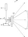
- FIG. 1 shows the basic configuration of the optical scanning apparatus according to the first embodiment of the present invention.
- the optical scanning apparatus is composed of a light source 151 made of a semiconductor laser, a diffraction element 161 composed of a support 131 and a liquid crystal diffraction element 121 arranged on at least one surface of the support 131, and a light source. It is provided with an optical deflector 101 that deflects the emitted light source.
- the diffraction element 161 and the light deflector 101 correspond to the light deflector in the present invention.
- the liquid crystal diffraction element 121 corresponds to the optically anisotropic layer in the present invention.
- FIG. 1 is an example of an optical scanning device that uses a MEMS (Micro Electro Mechanical Systems) optical deflector as the optical deflector 101.
- MEMS Micro Electro Mechanical Systems
- the liquid crystal diffusing element 121 is a cured layer of the liquid crystal composition, the optical axis of the liquid crystal compound contained in the liquid crystal composition is parallel to the main surface of the liquid crystal diffusing element, and the liquid crystal diffusing element is in the plane thereof. It is a liquid crystal alignment pattern arranged along at least one direction, and has a liquid crystal alignment pattern in which the orientation of the optical axis of the liquid crystal compound is continuously changed by rotation.
- the liquid crystal diffraction element diffracts the incident light by having a liquid crystal orientation pattern.
- the diffraction angle of light by the liquid crystal diffraction element is the length of one cycle p in which the direction of the optical axis of the liquid crystal compound is rotated by 180 ° in the liquid crystal alignment pattern (hereinafter, also simply referred to as “one cycle p”).
- one cycle p the longer the period p, the larger the diffraction angle.
- the laser beam emitted from the light source 151 is deflected in the direction of the diffraction element 161 by the optical deflector 101.
- the deflected light enters any place of the diffraction element 161 and is diffracted in a desired direction such as by expanding the deflection angle of the light by the diffraction element 161 to function as the optical scanning device 100.
- the optical deflector 101 controls the deflection angle incident on the diffraction element by the controller 141.
- a reflection mirror, a condenser lens, a deflector, a retardation plate, etc. may be appropriately inserted in the optical path.
- the optical scanning device 100 deflects the light emitted by the light source 151 by an optical deflector 101 at a predetermined angle.
- the polarization angle by the optical deflector 101 is appropriately changed by the controller 141, the traveling direction of the light is changed, and scanning using the light is performed.
- the light deflected by the light deflector 101 is diffracted by the diffraction element 161 to expand the deflection angle as shown in the illustrated example. Therefore, the scanning range is expanded.
- the wavelength of the laser beam mainly used as a light source has a temperature dependence, and generally has a characteristic that the oscillation wavelength shifts to the long wavelength side due to a temperature rise.
- the degree of change is about +8 nm with an increase of 40 ° C. That is, when a 940 nm laser is used and the temperature of the light source rises by 40 ° C., the oscillation wavelength of the light source becomes about 948 nm.
- the diffraction angle by the diffraction element changes depending on the wavelength of light.
- the diffraction angle of light by the liquid crystal diffraction element depends on one cycle p of the liquid crystal alignment pattern. Therefore, when the liquid crystal diffraction element expands in the plane direction due to the temperature rise, one cycle p becomes longer and the diffraction angle becomes smaller. Therefore, it is conceivable that the increase in the deflection angle due to the increase in the oscillation wavelength of the light source is offset by the decrease in the diffraction angle due to the expansion of the liquid crystal diffraction element to make the deflection angle constant regardless of the temperature.
- the liquid crystal diffraction element is formed by polymerizing a liquid crystal compound, and its thickness is several microns to several tens of microns.
- a support having a liquid crystal diffraction element on at least one surface has a size of several hundred microns or more, and has a higher elastic modulus than a liquid crystal diffraction element obtained by polymerizing a liquid crystal compound. Therefore, when the liquid crystal diffraction element and the support expand and contract with the temperature fluctuation, the expansion and contraction of the liquid crystal diffraction element is regulated by the support, and the state of the liquid crystal diffraction element is mainly controlled by the expansion and contraction of the support. ..
- the diffraction angle of the diffraction element due to the temperature fluctuation is mainly controlled by the thermal characteristics of the support that the liquid crystal diffraction element follows, not the thermal characteristics of the liquid crystal diffraction element itself.
- the coefficient of linear expansion of the support is related to the following conditional expression (1), the influence of the wavelength increment of the light source can be suppressed.
- This conditional expression (1) stipulates that the deviation of the scanning angle is less than 0.3 °.
- the support satisfies this conditional expression (1), the scanning angle deviation due to temperature fluctuation can be reduced.
- the scanning angle deviation will be described by giving specific numerical values.
- the linear expansion coefficient of the support is small, for example, when it is zero, the emission angle with respect to the incident angle of 30 °. Is changed from 60 ° to 60.4 °, and the scanning angle deviation is 0.4 °.
- the coefficient of linear expansion of the support is zero, the left side of the conditional expression (1) is about 2.1 ⁇ 10 -4 , which does not satisfy the conditional expression (1).
- the scanning angle deviation is 0.3 ° or less, and when the coefficient of linear expansion is 100 ppm / ° C, the scanning angle deviation is 0.2 ° or less.
- the scanning angle deviation is approximately 0. This makes it possible to realize an optical scanning device that is resistant to temperature fluctuations.
- the coefficient of linear expansion of the support is 50 ppm / ° C.
- the left side of the conditional expression (1) is about 1.6 ⁇ 10 -4 , which satisfies the conditional expression (1).
- the left side of the conditional expression (1) is about 1.1 ⁇ 10 -4 , which satisfies the conditional expression (1).
- the coefficient of linear expansion of the support is 200 ppm / ° C.
- the left side of the conditional expression (1) is about 0.1 ⁇ 10 -4 , which satisfies the conditional expression (1).
- the configuration is such that the MEMS optical deflector is provided as the optical deflector 101, but the present invention is not limited to this, and the optical deflector 101 deflects the incident light by a predetermined angle and deflects the incident light. Anything that can change the angle will do.
- a liquid crystal optical phase modulation element is provided as the optical deflector 101.
- the optical scanning device 100 includes a light source (not shown) arranged on the left side of the optical deflector 101 in the figure, an optical deflector 101, a diffraction element 161 and a controller 141.
- the liquid crystal optical phase modulation element controls the deflection direction of incident light by applying a voltage to the liquid crystal layer to control the orientation of the liquid crystal in the liquid crystal layer.
- FIG. 3 is a conceptual diagram for explaining the operation of the optical scanning device 100 shown in FIG.
- the liquid crystal optical phase modulation element 101 deflects the light emitted from a light source (not shown) by a predetermined angle (see the solid arrow).
- the polarization angle of the liquid crystal optical phase modulation element 101 is changed by the controller 141. That is, as shown by the arrow of the broken line in FIG. 3, the polarization angle by the liquid crystal optical phase modulation element 101 is appropriately changed by the controller 141 to change the traveling direction of the light. As a result, the traveling direction of the light is changed, and the optical scanning device 100 performs scanning using the light.
- the light deflected by the light deflector 101 is diffracted by the diffraction element 161 to expand the deflection angle as shown in the illustrated example. Therefore, the scanning range is expanded.
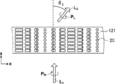
- the liquid crystal diffraction element 120 of the diffraction element 161 has a region (120a to 120e) in which one cycle of the liquid crystal alignment pattern is different in the plane.
- the smaller one cycle of the liquid crystal alignment pattern the larger the diffraction angle.
- the diffraction angle of the liquid crystal diffraction element 120 is gradually increased from the center of the deflection by the optical deflector 101 toward the outside (both ends). .. This means that, in FIG.
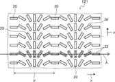
- FIG. 4 conceptually shows an example of the diffraction element 161.
- FIG. 4 is a view of the diffraction grating 161 viewed in the same direction as FIGS. 1 to 3, and is a side view of the diffraction grating 161.
- the diffraction element 161 is in the form of a sheet, and has a support 131, an alignment film 13, and an optically anisotropic layer (liquid crystal diffraction element) 121.
- the liquid crystal diffraction element 121 further deflects the light deflected by the optical deflector 101 by diffracting the light deflected by the optical deflector 101 in the deflection direction by the optical deflector 101.
- the sheet surface direction of the liquid crystal diffraction element 121 is defined as the xy direction, and the thickness direction is defined as the z direction. In FIG.
- the horizontal direction in the figure is the direction in which the optic axis derived from the liquid crystal compound rotates in one direction (axis A direction described later), and this direction is defined as the x direction. Therefore, the y direction is a direction orthogonal to the paper surface of FIG.
- the liquid crystal diffraction element 121 is planar, but the liquid crystal diffraction element 121 is not limited to a planar shape and may be a curved surface.
- ⁇ Support> As the support 131, various sheet-like materials (films, plate-like materials) can be used as long as the coefficient of thermal expansion satisfies a predetermined condition and the alignment film and the optically anisotropic layer can be supported.
- a transparent support is preferable, and examples thereof include a polyacrylic resin film such as polymethylmethacrylate, a cellulosic resin film such as cellulose triacetate, and a cycloolefin polymer film.
- the cycloolefin polymer-based film include the trade name "Arton” manufactured by JSR Corporation and the trade name "Zeonoa” manufactured by Zeon Corporation.
- the coefficient of linear expansion is a constant peculiar to the material, and the value of the coefficient of linear expansion can be adjusted as a composite material by mixing a plurality of materials or forming a laminated structure.
- the support 131 has anisotropy in the thermal expansion direction, it is desirable that the support 131 be parallel or perpendicular to the periodic direction of the diffraction element.
- the linear expansion coefficient may be high in the stretching direction. In that case, it is desirable that the stretching direction and the periodic direction of the diffraction element be parallel. In the opposite case, it is desirable that the stretching direction and the periodic direction of the diffraction element are orthogonal to each other.
- an alignment film 13 is formed on the surface of the support 131.
- the alignment film 13 is an alignment film for orienting the liquid crystal compound 20 in a predetermined liquid crystal alignment pattern when forming the optically anisotropic layer 121.
- the optically anisotropic layer 121 changes the orientation of the optical axis 22 derived from the liquid crystal compound 20 while continuously rotating along one direction in the plane. Has a pattern. Therefore, the alignment film 13 is formed so that the optically anisotropic layer 121 can form this liquid crystal alignment pattern.
- the direction of the optical axis 22 rotates 180 ° in one direction (direction along the axis A described later) in which the direction of the optical axis 22 changes while continuously rotating in the liquid crystal alignment pattern.
- the length to be used is one cycle (rotation cycle p of the optic axis 22).
- one cycle of the optically anisotropic layer 121 is gradually shortened from the center of the deflection (deflection direction (deflection direction)) by the optical deflector 101 toward the outside. Further, the rotation direction of the optical axis of the liquid crystal compound 20 is reversed at the center of deflection by the optical deflector 101 in the direction along the axis A (arrow x direction). Therefore, the alignment film 13 is formed so that the optically anisotropic layer 121 can form this liquid crystal alignment pattern.
- the alignment film 13 various known ones can be used.
- the alignment film 13 include a rubbing-treated film made of an organic compound such as a polymer, an oblique vapor-deposited film of an inorganic compound, a film having microgrooves, and ⁇ -tricosanoic acid, dioctadecylmethylammonium chloride, and methyl stearylate.
- Examples thereof include a membrane obtained by accumulating LB (Langmuir-Blodgett) membranes obtained by the Langmuir-Blodget method of organic compounds.
- Examples of the alignment film 13 include those formed by rubbing the surface of the polymer layer. The rubbing treatment is carried out by rubbing the surface of the polymer layer with paper or cloth several times in a certain direction.
- the types of polymers used for the alignment film are polyimide, polyvinyl alcohol, polymers having a polymerizable group described in JP-A-9-152509, JP-A-2005-97377, JP-A-2005-99228, and JP-A-2005-99228.
- the alignment film described in JP-A-2005-128503 can be preferably used.
- the orthogonal alignment film referred to in the present invention means an alignment film in which the major axis of the molecule of the polymerizable rod-shaped liquid crystal compound is oriented so as to be substantially orthogonal to the rubbing direction of the orthogonal alignment film.
- the thickness of the alignment film does not have to be thick as long as it can provide the alignment function, and is preferably 0.01 to 5 ⁇ m, more preferably 0.05 to 2 ⁇ m.
- a so-called photo-alignment film in which a photo-alignable material is irradiated with polarized light or non-polarized light to form an alignment film can also be used. That is, a light alignment material may be applied onto the support 131 to form a photoalignment film.
- Polarized light irradiation can be performed from a vertical direction or an oblique direction with respect to the photoalignment film, and non-polarized light irradiation can be performed from an oblique direction with respect to the photoalignment film.
- Examples of the photoalignment material used for the photoalignment film that can be used in the present invention include JP-A-2006-285197, JP-A-2007-76839, JP-A-2007-138138, and JP-A-2007-94071.
- JP-A-9-118717 JP-A-10-506420, JP-A-2003-505561, WO2010 / 150748, JP-A-2013-177561, and JP-A-2014.
- Preferred examples thereof include photodimerizable compounds described in JP-A-12823, particularly cinnamate compounds, chalcone compounds and coumarin compounds.
- Particularly preferred are azo compounds, photocrosslinkable polyimides, polyamides, esters, cinnamate compounds, and chalcone compounds.
- FIG. 8 shows a schematic view of an alignment film exposure apparatus in which the photoalignment material is applied onto the support 131 and dried, and then the alignment film is exposed to form an alignment pattern.
- the exposure apparatus 50 is arranged on the light path 54 of the light source 54 provided with the laser 52, the polarization beam splitter 56 that separates the laser beam 70 from the laser 52 into two, and the two separated rays 72A and 72B, respectively.
- Mirrors 58A, 58B and ⁇ / 4 plates 60A, 60B are provided.
- the light source 54 emits linearly polarized light P 0 .
- lambda / 4 plate 60A is linearly polarized light P 0 on the right circularly polarized light P R
- lambda / 4 plate 60B converts the linearly polarized light P 0 to the left circularly polarized light P L.
- a support 131 having an alignment film 13 before the alignment pattern is formed is arranged in the exposed portion, and two light rays 72A and 72B are crossed and interfered with each other on the alignment film 13, and the interference light is transmitted to the alignment film 13. Irradiate and expose. Due to the interference at this time, the polarization state of the light applied to the alignment film 13 changes periodically in the form of interference fringes. As a result, an orientation pattern in which the orientation state changes periodically can be obtained. In the exposure apparatus 50, the period of the orientation pattern can be changed by changing the intersection angle ⁇ of the two rays 72A and 72B.
- the optic axis 22 rotates in one direction.
- the optically anisotropic layer 121 which will be described later, on the alignment film 13 having the alignment pattern in which the orientation state changes periodically in this way, the optical anisotropy provided with the liquid crystal alignment pattern corresponding to this period.
- Layer 121 can be formed.
- the rotation direction of the optical shaft 22 can be reversed by rotating the optical axes of the ⁇ / 4 plate 60A and the ⁇ / 4 plate 60B by 90 °, respectively.
- the exposure apparatus 80 shown in FIG. 9 is an exposure apparatus that is also used when forming a concentric liquid crystal alignment pattern as shown in FIG. 7.
- the exposure apparatus 80 includes a light source 84 provided with a laser 82, a polarization beam splitter 86 that splits the laser beam M from the laser 82 into S-polarized light MS and P-polarized light MP, and a mirror 90A arranged in the optical path of the P-polarized light MP.
- the P-polarized MP divided by the polarizing beam splitter 86 is reflected by the mirror 90A and incident on the polarizing beam splitter 94.
- the S-polarized light MS split by the polarizing beam splitter 86 is reflected by the mirror 90B, focused by the lens 92, and incident on the polarizing beam splitter 94.
- the P-polarized MP and the S-polarized MS are combined by a polarizing beam splitter 94 and become right-circularly polarized light and left-handed circularly polarized light according to the polarization direction by the ⁇ / 4 plate 96, and the alignment film 13 on the support 131. It is incident on.
- the polarization state of the light applied to the alignment film 13 periodically changes in an interference fringe pattern. Since the intersection angle of the left-handed circularly polarized light and the right-handed circularly polarized light changes from the inside to the outside of the concentric circles, an exposure pattern in which the pitch changes from the inside to the outside can be obtained. As a result, in the alignment film 13, a concentric alignment pattern in which the alignment state changes periodically can be obtained.
- the length of one cycle (rotation cycle p) in which the optical axis 22 of the liquid crystal compound 20 continuously rotates 180 ° along one direction is the refractive power of the lens 92 (F number of the lens 92). It can be controlled by changing the focal length of the lens 92, the distance between the lens 92 and the alignment film 13, and the like.
- the length of one cycle in which the optic axis 22 rotates 180 ° in one direction in which the optic axis 22 continuously rotates can be changed.
- the length of one cycle in which the optic axis 22 rotates 180 ° can be changed depending on the degree of focusing of the light transmitted through the lens 92 that interferes with the parallel light. More specifically, when the refractive power of the lens 92 is weakened, it approaches parallel light, so that the length of one cycle in which the optic axis 22 rotates 180 ° gradually shortens from the inside to the outside, and the F number becomes growing.
- the refractive power of the lens 92 is increased, the length of one cycle in which the optical axis 22 rotates by 180 ° suddenly shortens from the inside to the outside, and the F number becomes small.
- the configuration in which one cycle (rotation cycle p) in which the optic axis 22 rotates 180 ° in one direction in which the optic axis 22 continuously rotates is changed, the liquid crystal compound 20 is formed in only one direction in the direction of arrow X. It can also be used in a configuration in which the optical shaft 22 continuously rotates and changes. For example, by gradually shortening one cycle in which the optical axis 22 rotates by 180 ° in the direction of the arrow X, an optical element that transmits light so as to be focused can be obtained.
- liquid crystal alignment pattern by reversing the direction in which the optical axis 22 rotates by 180 °, it is possible to obtain an optical element that transmits light so as to diffuse only in the direction of arrow X. By reversing the turning direction of the incident circularly polarized light, it is possible to obtain an optical element that transmits light so as to diffuse only in the X direction of the arrow.
- one cycle in which the optical axis 22 rotates 180 ° in the arrow X direction is not gradually changed depending on the application of the optical element, but in the arrow X direction. It is also possible to use a configuration in which the optical axis 22 is partially rotated by 180 ° and has regions having different cycles. For example, as a method of partially changing one cycle in which the optic axis 22 rotates 180 °, a method of scanning and exposing a photoalignment film and patterning while arbitrarily changing the polarization direction of the focused laser light is used. be able to.
- the alignment film 13 is provided as a preferable embodiment, and is not an indispensable constituent requirement.
- the optically anisotropic layer 121 is derived from the liquid crystal compound 20 by forming an orientation pattern on the support 131 by a method of rubbing the support 131, a method of processing the support 131 with a laser beam, or the like. It is also possible to have a configuration having a liquid crystal orientation pattern in which the orientation of the optical axis 22 is changing while continuously rotating along at least one direction in the plane.
- an optically anisotropic layer (liquid crystal diffraction element) 121 which is a cured layer of the liquid crystal composition containing the liquid crystal compound 20, is provided on the surface of the alignment film 13.
- the optical axes (slow-phase axes) of the liquid crystal compound are liquid crystal patterns arranged along at least one direction in the plane of the optically anisotropic layer, and the optics of the liquid crystal compound 20
- the axis 22 has a liquid crystal orientation pattern in which the orientation changes in one direction.
- the retardation R is preferably 0.4 ⁇ to 0.6 ⁇ , more preferably 0.45 ⁇ to 0.55 ⁇ , and particularly preferably 0.5 ⁇ .
- ⁇ n is the birefringence of the optically anisotropic layer 121
- d1 is the thickness.
- the liquid crystal diffraction element 121 functions as a transmission type diffraction grating.
- the principle of functioning as a diffraction grating will be described with reference to FIGS. 4 to 6.
- FIG. 5 is a schematic plan view of the optically anisotropic layer 121, that is, FIG. 4 is a view of FIG. 4 viewed from above in the drawing.
- the liquid crystal compound 20 is immobilized in a liquid crystal orientation pattern in which the optical axis 22 is continuously rotated in one direction.
- the optic axis 22 continuously changes in rotation in the direction along the axis A in FIG. 5, which coincides with the arrow x direction. That is, the liquid crystal compound 20 is oriented so that the angle formed by the in-plane component of the long axis (axis of abnormal light: director) of the liquid crystal compound 20 defined as the optical axis 22 and the axis A changes in rotation. ..
- FIG. As shown in FIG.
- the direction of the optical axis 22 of the liquid crystal compound 20 coincides with that of the liquid crystal compound 20 arranged in the direction orthogonal to the axis A, that is, in the direction of the arrow y.
- the optically anisotropic layer 121 exhibits the function as a general ⁇ / 2 plate as described above for each region where the directions of the optical axes 22 of the liquid crystal compound 20 in the y direction coincide with each other.
- the angle formed by the optical axis 22 and the axis A of the liquid crystal compound 20 arranged along the axis A differs depending on the position in the axis A direction. It is a pattern oriented and fixed so that the angle formed by the optic axis 22 and the axis A gradually changes from ⁇ to ⁇ + 180 ° or ⁇ -180 ° along the axis A.
- the optical axis 22 of the liquid crystal compound 20 is parallel to the plane of the optically anisotropic layer 121, and the direction of the optical axis 22 is constant.
- a local region that is, a region in which the liquid crystal compound 20 is arranged in the y direction of the arrow is arranged in the x direction orthogonal to the y direction of the arrow, and is arranged among a plurality of local regions arranged in the x direction of the arrow.
- a liquid crystal alignment pattern in which the direction of the optical axis 22 is continuously rotationally changed in one direction (direction along the axis A) is referred to as horizontal rotational orientation.
- the angle change of the optic axis 22 toward the axis A direction may be a thing that rotates at a non-uniform angle interval instead of a constant angle interval.
- the average value of the orientation of the optical axis 22 in the unit region changes linearly at a constant rate, it means that the value gradually changes.
- the change in the inclination of the optical axis between the unit regions adjacent to the axis A direction in which the optical axes 22 have different inclinations is preferably 45 ° or less. It is preferable that the change in the slope of the adjacent unit region is smaller.
- the distance at which the angle formed by the optical axis 22 and the axis A changes from ⁇ to ⁇ + 180 ° (returns to the original) toward the axis A direction that is, the period during which the optical axis 22 rotates 180 °.
- the rotation cycle (1 cycle) p is preferably 0.1 to 5 ⁇ m. The shorter the rotation period p, the larger the diffraction angle by the optically anisotropic layer 121, that is, the liquid crystal diffraction element 121. Therefore, the rotation period p may be determined according to the wavelength of the incident light on the liquid crystal diffraction element 121 and the desired emission angle.
- the diffraction element 161 gives a phase difference of ⁇ / 2 with respect to the incident light, and emits the incident light incident at an incident angle of 0 °, that is, the vertically incident incident light at an emission angle ⁇ . Emit with 2. That is, as shown in FIG. 6, the optical when the perpendicular plane of the anisotropic layer 121 with light L 1 of the right circularly polarized light P R is incident, left circular polarization P L in the direction forming an normal direction and the angle theta 2 Light L 2 is emitted.
- injecting light perpendicularly to the surface of the optically anisotropic layer 121 means, in other words, injecting light along the normal of the surface.
- injecting light perpendicularly to the surface of the optically anisotropic layer 121 means, in other words, injecting light along the normal of the surface.
- incident light L 1 light L 1 of the right circularly polarized light P R that is incident on the optically anisotropic layer 121.
- emitted light L 2 light L 2 of the left-handed circularly polarized light P L emitted from the optical anisotropic layer.
- the exit angle of the outgoing light L 2 is the angle formed by the normal direction of the optically anisotropic layer 121 and the outgoing light L 2 is.
- the diffraction direction of the light L 2 emitted from the liquid crystal diffraction element 121 is the circularly polarized light of the light incident on the liquid crystal diffraction element 121.
- the state is controlled to cause incident. That is, as shown in the illustrated example, when the incident light is linearly polarized light, the direction of diffraction of the light is either by inserting a ⁇ / 4 plate, converting it to circularly polarized light on either the left or right side, and then incident light. Can only be.
- the wavelength ⁇ of the light that causes the diffraction action by the liquid crystal diffraction element (optically anisotropic layer) 121 may be from ultraviolet to visible light, infrared light, or even an electromagnetic wave level.
- the liquid crystal compound 20 a rod-shaped liquid crystal compound and a disk-shaped liquid crystal compound can be used.
- the rotation cycle may be designed so that a desired diffraction angle ⁇ 2 can be obtained so as to satisfy the above equation (1) in consideration of the incident angle ⁇ 1.
- the light deflected by the optical deflector 101 is diffracted by the diffraction element 161 (optical anisotropic layer 121), so that the maximum deflection angle ⁇ of the optical deflector 101 is ⁇ . It enables the deflection of light by the deflection angle of the maximum emission angle ⁇ max out, which is much larger than max.
- the diffraction angle of light by the optically anisotropic layer 121 increases as one cycle in which the optical axis 22 of the liquid crystal compound 20 rotates by 180 °, that is, the rotation cycle p is shorter.
- the deflection direction (swirl direction) of the incident circular polarization is the same, the diffraction direction of the light by the optically anisotropic layer 121 is opposite depending on the rotation direction of the optical axis 22 of the liquid crystal compound 20. That is, when the incident light L 1 is a right circularly polarized light P R, as viewed from the exit surface side, the rotational direction of the optical axis 22, in the axial direction A (direction of arrow x) as shown in FIGS. 4 to 6 When clockwise, the emitted light L 2 is diffracted, for example, in the axis A direction.
- the incident light L 1 is a right circularly polarized light P R, as viewed from the exit side, when the rotation direction of the optical axis 22 is a counterclockwise toward the axis A direction, The emitted light L 2 is diffracted in the direction opposite to the axis A direction (direction of the arrow).
- the optically anisotropic layer 121 deflects the rotation period p of the optical axis 22 of the liquid crystal compound 20 toward the axis A direction by the optical deflector 101 (deflection direction). ) Gradually shorten from the center to the outside. That is, the diffraction angle of light by the optically anisotropic layer 121 increases toward the outside in the deflection direction.
- the optically anisotropic layer 121 reverses the rotation direction of the optical axis 22 of the liquid crystal compound 20 toward the axis A direction at the center of deflection by the optical deflector 101. ..
- the rotation direction of the optical axis 22 toward the axis A direction is counterclockwise from the upstream side in the axis A direction to the center in the deflection direction toward the axis A direction, and the center of deflection.
- the rotation direction of the optical shaft 22 is reversed, and the rotation direction of the optical shaft 22 toward the axis A direction is clockwise from the center of deflection toward the downstream in the axis A direction.
- the rotation direction of the optical axis 22 is usually reversed at the center of the optically anisotropic layer 121 in the axis A direction (arrow x direction), that is, in one direction in which the optical axis 22 rotates. That is, in the optical scanning apparatus 100, the center of deflection in the optical deflector 101 is usually aligned with the center of the optically anisotropic layer 121 in the axis A direction.
- the rotation period p may be continuously shortened from the center of deflection toward the outside, or may be gradually shortened.
- the optically anisotropic layer 121 is formed, for example, by a liquid crystal composition containing a liquid crystal compound.
- the liquid crystal composition containing the liquid crystal compound for forming the optically anisotropic layer 121 contains other components such as a leveling agent, an orientation control agent, a polymerization initiator and an orientation aid in addition to the liquid crystal compound. You may.
- the optically anisotropic layer 121 is composed of a cured layer of a liquid crystal composition containing a rod-shaped liquid crystal compound or a disk-shaped liquid crystal compound, and the optical axis of the rod-shaped liquid crystal compound or the optical axis of the disk-shaped liquid crystal compound is oriented as described above. It has a liquid crystal orientation pattern.
- the present invention includes an embodiment in which a laminate integrally provided with a support 131 and an alignment film functions as a ⁇ / 2 plate.
- the liquid crystal composition for forming the optically anisotropic layer contains a rod-shaped liquid crystal compound or a disk-shaped liquid crystal compound, and further contains other components such as a leveling agent, an orientation control agent, a polymerization initiator, and an orientation aid. May be contained.
- the optically anisotropic layer preferably has a wide band with respect to the wavelength of the incident light, and is preferably formed by using a liquid crystal material having a birefringence of inverse dispersion. Further, it is also preferable to impart a twisting component to the liquid crystal composition and to laminate different retardation layers so that the optically anisotropic layer has a substantially wide band with respect to the wavelength of the incident light.
- a method of realizing a wide-band patterned ⁇ / 2 plate by laminating two layers of liquid crystals having different twist directions is shown in Japanese Patent Application Laid-Open No. 2014-089476 and the like. , Can be preferably used in the present invention.
- rod-shaped liquid crystal compound examples include azomethines, azoxys, cyanobiphenyls, cyanophenyl esters, benzoic acid esters, cyclohexanecarboxylic acid phenyl esters, cyanophenylcyclohexanes, cyano-substituted phenylpyrimidines, alkoxy-substituted phenylpyrimidines, and the like. Phenyldioxans, trans, and alkenylcyclohexylbenzonitriles are preferably used. Not only low molecular weight liquid crystal molecules as described above, but also high molecular weight liquid crystal molecules can be used.
- the polymerizable rod-shaped liquid crystal compound examples include Makromol. Chem., 190, 2255 (1989), Advanced Materials 5, 107 (1993).
- US Pat. Nos. 4,683,327, 562,648, 5770107, International Publication 95/22586, 95/24455, 97/00600, 98/23580, 98/52905 , JP-A No. 1-272551, No. 6-16616, No. 7-110469, No. 11-8801, and Japanese Patent Application No. 2001-64627 can be used.
- the rod-shaped liquid crystal compound for example, those described in JP-A No. 11-513019 and JP-A-2007-279688 can also be preferably used.
- the disk-shaped liquid crystal compound for example, those described in JP-A-2007-108732 and JP-A-2010-244038 can be preferably used.
- the liquid crystal compound 20 rises in the thickness direction in the optically anisotropic layer, and the optical axis 22 derived from the liquid crystal compound has a disk surface. It is defined as the axis perpendicular to, the so-called phase-advancing axis.
- the optically anisotropic layer 121 can be formed by coating a liquid crystal composition on the alignment film 13 in multiple layers.
- a liquid crystal composition is applied on an alignment film, heated, cooled, and then cured by ultraviolet rays to prepare a first liquid crystal immobilization layer, and then the second and subsequent layers are fixed to the liquid crystal. It refers to repeating the process of overcoating the liquid crystal layer, applying it, heating it in the same manner, cooling it, and then curing it with ultraviolet rays.
- the optically anisotropic layer 121 by coating the layers as described above, even when the total thickness of the optically anisotropic layer 121 is increased, the orientation direction of the alignment film 13 can be changed to the optically anisotropic layer 121. It can be reflected from the lower surface to the upper surface of.
- FIG. 7 is a schematic plan view of the optically anisotropic layer in the design modification example of the liquid crystal diffraction element.
- the liquid crystal alignment pattern in the optically anisotropic layer 122 shown in FIG. 7 is different from the liquid crystal alignment pattern in the optically anisotropic layer 121 described above. In FIG. 7, only the optical axis 22 is shown.
- the optically anisotropic layer 122 of FIG. 7 is a liquid crystal in which the direction of the optical axis 22 gradually rotates and changes along multiple directions from the center side to the outside, for example, axes A 1 , A 2 , A 3, and so on. It has an orientation pattern. That is, the liquid crystal alignment pattern of the optically anisotropic layer 122 shown in FIG.
- the liquid crystal alignment pattern of the optically anisotropic layer 122 shown in FIG. 7 is a concentric pattern having one direction in which the direction of the optical axis changes while continuously rotating, in a concentric pattern from the inside to the outside. Is. Due to the liquid crystal alignment pattern shown in FIG. 7, the absolute phase of the incident light changes by a different amount of change between the local regions in which the directions of the optical axes 22 are different. If a liquid crystal orientation pattern in which the optical axis rotates in a radial manner as shown in FIG. 7 is provided, the incident light can be transmitted as divergent light or condensed light. That is, the function as a concave lens or a convex lens can be realized by the liquid crystal alignment pattern in the optically anisotropic layer 121.
- the function of the concave lens of the optically anisotropic layer 122 shown in FIG. 7 is used for the diffraction element 161.
- the maximum deflection angle ⁇ max emitted from the optical deflector 101 can be spread most efficiently.
- the value is finite to the extent that there is no practical problem depending on the beam diameter of the laser beam to be irradiated. May be good. For example, it may be about 10 to several hundred ⁇ m.
- the liquid crystal compound of the liquid crystal diffraction element is oriented in one direction in the thickness direction, but the present invention is not limited to this.
- the optically anisotropic layer constituting the liquid crystal diffraction element may have a liquid crystal compound twisted or oriented along a spiral axis extending along the thickness direction. Further, a plurality of liquid crystal layers having different twist orientation directions may be laminated. In this case, the tolerance for the incident angle and wavelength of light is widened.
- a diffraction element 162 having an optically anisotropic layer 122 functioning as a concave lens and an optical deflector that deflects light radially as an optical deflector A vessel 102 is used.
- the light deflector 102 deflects light at, for example, an orientation of 360 ° and a polar angle of 0 to 35 °.
- the optical scanning device may preferably include a condenser lens 110 as a condenser element, a ⁇ / 4 plate 111, and a condenser lens 112.
- the condensing lens 110 is a known condensing lens that slightly condenses the light incident on the liquid crystal diffraction element. By having the condenser lens 110, the light (light beam) emitted from the optical scanning device 100 (liquid crystal diffraction element 122) can be made into appropriate parallel light, and the straightness can be improved.
- a MEMS optical deflector described in Japanese Patent Application Laid-Open No. 2012-208352, Japanese Patent Application Laid-Open No. 2014- Light is emitted by swinging a mirror using a piezoelectric actuator or the like, such as the MEMS optical deflector described in Japanese Patent Application Laid-Open No. 134642 and the MEMS optical deflector described in Japanese Patent Application Laid-Open No. 2015-22064.
- the optical scanning apparatus of the present invention has a simple structure, a simple drive, and a large angle deflection, it can be applied to all applications for scanning light for which light weight and miniaturization are desired.
- a drawing device using a beam scan, a beam scan type projection display, a beam scan type head-up display, a beam scan type AR glass, and the like In this case, it can be applied as a device that deflects light in a wide wavelength range including visible light.
- the optical deflector is not limited to the above-mentioned MEMS optical deflector and liquid crystal optical phase modulator, and is a galvano mirror, a polygon mirror, and an optical phased array deflector (optical phase modulator). ) Etc., various known light deflectors can be used. Among them, the MEMS optical deflection element and the optical phased array deflection element described above are preferably used as the optical deflector in that the mechanical movable portion is small and the mechanical movable portion is small.
- Coating liquid for forming an alignment film ⁇ Material for photo-alignment A 1.00 parts by mass Water 16.00 parts by mass Butoxyethanol 42.00 parts by mass Propylene glycol monomethyl ether 42.00 parts by mass ⁇ ⁇
- the alignment film was exposed using the exposure apparatus shown in FIG. 9 to form an alignment film P-1 having an alignment pattern.
- a laser that emits laser light having a wavelength (405 nm) was used.
- the exposure amount due to the interference light was set to 100 mJ / cm 2 .
- the refractive power of the lens (convex lens) is adjusted and the optically anisotropic layer is formed thereafter, the period of rotation of the optical axis of the liquid crystal compound in the optically anisotropic layer gradually increases from the center to the outside. , I tried to shorten it.
- composition A-1 was prepared as a liquid crystal composition for forming an optically anisotropic layer.
- Composition A-1 Liquid Crystal Compound L-1 100.00 parts by mass Polymerization initiator (BASF, Irgacure (registered trademark) 907) 3.00 parts by mass Photosensitizer (manufactured by Nippon Kayaku Co., Ltd., KAYACURE DETX-S) 1.00 parts by mass Leveling agent T-1 0.08 parts by mass Methyl ethyl ketone 313.0 parts by mass ⁇ ⁇
- the optically anisotropic layer was formed by coating the composition A-1 on the alignment film P-1 in multiple layers.
- multi-layer coating first, the composition A-1 of the first layer is coated on the alignment film, heated, cooled, and then cured by ultraviolet rays to prepare a liquid crystal-immobilized layer, and then the second and subsequent layers are immobilized with the liquid crystal. It refers to repeating the process of overcoating the layers, applying them, and then heating and cooling them in the same way, followed by UV curing.
- the orientation direction of the alignment film is reflected from the lower surface to the upper surface of the optically anisotropic layer even when the total thickness of the optically anisotropic layer is increased.
- the composition A-1 is applied on the alignment film P-1, the coating film is heated to 70 ° C. on a hot plate, then cooled to 25 ° C., and then pressed under a nitrogen atmosphere.
- the orientation of the liquid crystal compound was fixed by irradiating the coating film with an ultraviolet ray having a wavelength of 365 nm using a mercury lamp at an irradiation amount of 100 mJ / cm 2.
- the film thickness of the first liquid crystal immobilization layer was 0.2 ⁇ m.
- the second and subsequent layers were overcoated on the liquid crystal immobilization layer, heated under the same conditions as above, cooled, and then cured by ultraviolet rays to prepare a liquid crystal immobilization layer.
- the diffraction element having the support, the alignment film, and the optically anisotropic layer by repeatedly coating the grating until the total thickness reaches a desired film thickness to form the optically anisotropic layer.
- the optically anisotropic layer finally has a liquid crystal ⁇ n 940 ⁇ thickness (Re (940)) of 470 nm, and is optically anisotropic from the center to the outside in one direction in which the optic axis rotates.
- the rotation cycle of the optical axis of the liquid crystal compound in the layer was gradually shortened and that the rotation direction of the optical axis was reversed at the center.
- the rotation cycle (1 cycle) in which the optical axis of the liquid crystal compound rotates by 180 ° has a very large rotation cycle in the central portion (the inverse number of the rotation cycle is 0).
- the rotation cycle at a distance of 2.5 mm from the center is 10.6 ⁇ m
- the rotation cycle at a distance of 5.0 mm from the center is 5.3 ⁇ m
- the rotation cycle gradually shortens from the center to the outside. It was a liquid crystal orientation pattern.
- a 940 nm semiconductor laser was prepared as the light source laser. Further, a ⁇ / 4 plate (circular polarizing plate, Edmund) was prepared in order to convert the linearly polarized light of the laser into circularly polarized light and incident it on the liquid crystal diffraction element. ⁇ n 940 ⁇ d (Re (940)) was 470 nm. Further, a micromirror device was produced by the method described in Japanese Patent Application Laid-Open No. 2014-134642. The diameter of the mirror portion was 4 mm, and the deflection angle was ⁇ 35 °. These were configured as shown in FIG. 1 to produce an optical scanning device.
- the polarization direction of the laser beam and the in-plane slow-phase axis of the ⁇ / 4 plate were intersected at 45 ° so that they were converted into circularly polarized light.
- a condenser lens (convex lens) is arranged between the light source and the light deflector.
- the characteristic values of each optical component are as follows. The light diameter of the laser beam was 3 mm, the focal length of the condenser lens was 35 mm, the distance between the condenser lens and the MEMS was 16 mm, and the distance between the MEMS and the liquid crystal diffractometer was 7 mm.
- the range of the deflection angle of the emitted light by MEMS was ⁇ 35 °.
- the diameter of the liquid crystal diffraction element is 20 mm.
- the liquid crystal diffractometer has a very large rotation cycle at the center (the reciprocal of the rotation cycle is 0), the rotation cycle at a position with a radius of 5 mm is 4.8 ⁇ m, and the rotation cycle at a position with a radius of 10 mm is 2.6 ⁇ m.
- the center wavelength ⁇ 0 of the light source at 25 ° C. is 940 nm, and the increment d ⁇ of the center wavelength when the temperature rises by 40 ° C. is 8 nm. Since the coefficient of linear expansion of the support is 3 ppm / ° C., the left side of the conditional expression (1) is 2.07 ⁇ 10 -4 , which does not satisfy the conditional expression (1).
- Example 1 The liquid crystal diffraction grating of Example 1 was produced under the same conditions as in Comparative Example 1 except that the support of Comparative Example 1 was changed to Technoroy S001G manufactured by Sumika Acrylic Sales Co., Ltd., which is PMMA (polymethyl methacrylate resin). , An optical scanning device was manufactured. The coefficient of thermal expansion of PMMA was 70 ppm / ° C. In the configuration of the first embodiment, the left side of the conditional expression (1) is 1.4 ⁇ 10 -4 , which satisfies the conditional expression (1).
- Example 2 The liquid crystal diffraction grating of Example 2 was produced under the same conditions as in Example 1 except that the support of Example 1 was changed to ZF-4 manufactured by Nippon Zeon Corporation, which is a cycloolefin polymer (COP), and light scanning was performed. The device was made. The coefficient of thermal expansion of COP was 70 ppm / ° C. In the configuration of the second embodiment, the left side of the conditional expression (1) is 1.4 ⁇ 10 -4 , which satisfies the conditional expression (1).
- ZF-4 cycloolefin polymer
- Example 3 The liquid crystal diffraction grating of Example 3 was produced under the same conditions as in Example 1 except that the support of Example 1 was changed to V-1, manufactured by Tamapoli, which is a low-density polyethylene, and an optical scanning device was produced. ..
- the coefficient of thermal expansion of the low-density polyethylene was 180 ppm / ° C.
- the left side of the conditional expression (1) is 0.3 ⁇ 10 -4 , which satisfies the conditional expression (1).
- the deflection angle by the micromirror device is in the range of the angle of incidence on the diffraction element of -30 ° to + 30 °, and the light incident on the diffraction element is greatly expanded by the liquid crystal diffraction element from the range of the angle of incidence of -30 ° to + 30 °. It was confirmed that the light was emitted at a deflection angle of 60 °.
- the values obtained by measuring the linear expansion coefficient of the diffraction element of this device at room temperature of 25 ° and 65 ° are shown in the table below. In order to confirm the influence of the temperature fluctuation of this device, the change of the emission angle of 60 ° at the incident angle of 30 ° was evaluated by changing the temperature.
Abstract
Le but de la présente invention est de fournir un dispositif de balayage optique qui a une direction de balayage stable en fonction de la fluctuation de température d'un laser à semi-conducteur en étant pourvu d'un élément optique à cristaux liquides prédéterminé utilisant la caractéristique d'un coefficient de dilatation linéaire d'un support d'un élément de diffraction à cristaux liquides. Ce dispositif de balayage optique est pourvu d'une source de lumière (151) et d'un élément de déviation optique. L'élément de déviation optique comprend un support (131) et une couche optiquement anisotrope (121) étant une couche durcie d'une composition de cristaux liquides, et a un motif d'orientation de cristaux liquides dans lequel l'axe optique d'un composé de cristaux liquides inclus dans la composition de cristaux liquides est parallèle à une surface de la couche optiquement anisotrope, et la couche optiquement anisotrope (121) est disposée le long d'au moins une direction dans la surface de la couche optiquement anisotrope, et dans laquelle la direction de l'axe optique du composé à cristaux liquides change de façon continue. Le support (131) satisfait l'expression conditionnelle (1) : |dλ/(dt×λ0)-α| < 2×10⁻⁴.
Priority Applications (2)
| Application Number | Priority Date | Filing Date | Title |
|---|---|---|---|
| JP2021567713A JP7367064B2 (ja) | 2019-12-26 | 2020-12-25 | 光走査装置 |
| US17/849,167 US11860504B2 (en) | 2019-12-26 | 2022-06-24 | Optical scanning device |
Applications Claiming Priority (2)
| Application Number | Priority Date | Filing Date | Title |
|---|---|---|---|
| JP2019-236320 | 2019-12-26 | ||
| JP2019236320 | 2019-12-26 |
Related Child Applications (1)
| Application Number | Title | Priority Date | Filing Date |
|---|---|---|---|
| US17/849,167 Continuation US11860504B2 (en) | 2019-12-26 | 2022-06-24 | Optical scanning device |
Publications (1)
| Publication Number | Publication Date |
|---|---|
| WO2021132646A1 true WO2021132646A1 (fr) | 2021-07-01 |
Family
ID=76574741
Family Applications (1)
| Application Number | Title | Priority Date | Filing Date |
|---|---|---|---|
| PCT/JP2020/048962 WO2021132646A1 (fr) | 2019-12-26 | 2020-12-25 | Dispositif de balayage optique |
Country Status (3)
| Country | Link |
|---|---|
| US (1) | US11860504B2 (fr) |
| JP (1) | JP7367064B2 (fr) |
| WO (1) | WO2021132646A1 (fr) |
Citations (4)
| Publication number | Priority date | Publication date | Assignee | Title |
|---|---|---|---|---|
| JP2000002847A (ja) * | 1998-06-12 | 2000-01-07 | Canon Inc | 走査光学装置及びマルチビーム走査光学装置 |
| JP2002116314A (ja) * | 2000-10-06 | 2002-04-19 | Sankyo Seiki Mfg Co Ltd | 回折素子および光ピックアップ装置 |
| US20080292358A1 (en) * | 2007-05-25 | 2008-11-27 | Samsung Electronics Co., Ltd. | Optical scanning unit and electro-photographic image forming apparatus including the same |
| WO2019189675A1 (fr) * | 2018-03-29 | 2019-10-03 | 富士フイルム株式会社 | Dispositif de déviation de lumière et dispositif optique |
Family Cites Families (2)
| Publication number | Priority date | Publication date | Assignee | Title |
|---|---|---|---|---|
| JP3432085B2 (ja) | 1996-08-28 | 2003-07-28 | キヤノン株式会社 | 走査光学装置 |
| US8982313B2 (en) | 2009-07-31 | 2015-03-17 | North Carolina State University | Beam steering devices including stacked liquid crystal polarization gratings and related methods of operation |
-
2020
- 2020-12-25 JP JP2021567713A patent/JP7367064B2/ja active Active
- 2020-12-25 WO PCT/JP2020/048962 patent/WO2021132646A1/fr active Application Filing
-
2022
- 2022-06-24 US US17/849,167 patent/US11860504B2/en active Active
Patent Citations (4)
| Publication number | Priority date | Publication date | Assignee | Title |
|---|---|---|---|---|
| JP2000002847A (ja) * | 1998-06-12 | 2000-01-07 | Canon Inc | 走査光学装置及びマルチビーム走査光学装置 |
| JP2002116314A (ja) * | 2000-10-06 | 2002-04-19 | Sankyo Seiki Mfg Co Ltd | 回折素子および光ピックアップ装置 |
| US20080292358A1 (en) * | 2007-05-25 | 2008-11-27 | Samsung Electronics Co., Ltd. | Optical scanning unit and electro-photographic image forming apparatus including the same |
| WO2019189675A1 (fr) * | 2018-03-29 | 2019-10-03 | 富士フイルム株式会社 | Dispositif de déviation de lumière et dispositif optique |
Also Published As
| Publication number | Publication date |
|---|---|
| JP7367064B2 (ja) | 2023-10-23 |
| US11860504B2 (en) | 2024-01-02 |
| US20220326565A1 (en) | 2022-10-13 |
| JPWO2021132646A1 (fr) | 2021-07-01 |
Similar Documents
| Publication | Publication Date | Title |
|---|---|---|
| US20210208316A1 (en) | Optical element and light deflection device | |
| JP7015380B2 (ja) | 光偏向装置および光学装置 | |
| JP6968190B2 (ja) | 光学素子 | |
| US11480716B2 (en) | Optical element that functions as a liquid crystal diffraction lattice | |
| US7375887B2 (en) | Method and apparatus for correcting a visible light beam using a wire-grid polarizer | |
| JP6893553B2 (ja) | 光学素子および光学装置 | |
| JP7174041B2 (ja) | 光照射装置およびセンサー | |
| JPWO2020022504A1 (ja) | 光学素子の製造方法および光学素子 | |
| CN115605785A (zh) | 透射型液晶衍射元件 | |
| US20220179197A1 (en) | Light deflection device and optical device | |
| WO2019163944A1 (fr) | Élément optique | |
| WO2021157585A1 (fr) | Élément optique et dispositif d'affichage d'image | |
| WO2021132646A1 (fr) | Dispositif de balayage optique | |
| JP7425912B2 (ja) | 光偏向装置および光学装置 | |
| US20240027783A1 (en) | Beam combiner, method of forming alignment film, and method of manufacturing optical element | |
| WO2021157598A1 (fr) | Élément optique et dispositif d'affichage d'image | |
| WO2024048276A1 (fr) | Feuille et procédé de production d'élément optique à cristaux liquides |
Legal Events
| Date | Code | Title | Description |
|---|---|---|---|
| 121 | Ep: the epo has been informed by wipo that ep was designated in this application |
Ref document number: 20906475 Country of ref document: EP Kind code of ref document: A1 |
|
| ENP | Entry into the national phase |
Ref document number: 2021567713 Country of ref document: JP Kind code of ref document: A |
|
| NENP | Non-entry into the national phase |
Ref country code: DE |
|
| 122 | Ep: pct application non-entry in european phase |
Ref document number: 20906475 Country of ref document: EP Kind code of ref document: A1 |