WO2021157585A1 - Élément optique et dispositif d'affichage d'image - Google Patents
Élément optique et dispositif d'affichage d'image Download PDFInfo
- Publication number
- WO2021157585A1 WO2021157585A1 PCT/JP2021/003811 JP2021003811W WO2021157585A1 WO 2021157585 A1 WO2021157585 A1 WO 2021157585A1 JP 2021003811 W JP2021003811 W JP 2021003811W WO 2021157585 A1 WO2021157585 A1 WO 2021157585A1
- Authority
- WO
- WIPO (PCT)
- Prior art keywords
- liquid crystal
- diffraction element
- light
- light guide
- incident
- Prior art date
Links
Images


Classifications
-
- G—PHYSICS
- G02—OPTICS
- G02B—OPTICAL ELEMENTS, SYSTEMS OR APPARATUS
- G02B6/00—Light guides; Structural details of arrangements comprising light guides and other optical elements, e.g. couplings
- G02B6/0001—Light guides; Structural details of arrangements comprising light guides and other optical elements, e.g. couplings specially adapted for lighting devices or systems
- G02B6/0011—Light guides; Structural details of arrangements comprising light guides and other optical elements, e.g. couplings specially adapted for lighting devices or systems the light guides being planar or of plate-like form
- G02B6/0033—Means for improving the coupling-out of light from the light guide
- G02B6/005—Means for improving the coupling-out of light from the light guide provided by one optical element, or plurality thereof, placed on the light output side of the light guide
- G02B6/0051—Diffusing sheet or layer
-
- G—PHYSICS
- G02—OPTICS
- G02B—OPTICAL ELEMENTS, SYSTEMS OR APPARATUS
- G02B5/00—Optical elements other than lenses
- G02B5/30—Polarising elements
- G02B5/3016—Polarising elements involving passive liquid crystal elements
-
- G—PHYSICS
- G02—OPTICS
- G02B—OPTICAL ELEMENTS, SYSTEMS OR APPARATUS
- G02B27/00—Optical systems or apparatus not provided for by any of the groups G02B1/00 - G02B26/00, G02B30/00
- G02B27/01—Head-up displays
- G02B27/017—Head mounted
- G02B27/0172—Head mounted characterised by optical features
-
- G—PHYSICS
- G02—OPTICS
- G02B—OPTICAL ELEMENTS, SYSTEMS OR APPARATUS
- G02B30/00—Optical systems or apparatus for producing three-dimensional [3D] effects, e.g. stereoscopic images
-
- G—PHYSICS
- G02—OPTICS
- G02B—OPTICAL ELEMENTS, SYSTEMS OR APPARATUS
- G02B5/00—Optical elements other than lenses
- G02B5/18—Diffraction gratings
-
- G—PHYSICS
- G02—OPTICS
- G02B—OPTICAL ELEMENTS, SYSTEMS OR APPARATUS
- G02B5/00—Optical elements other than lenses
- G02B5/18—Diffraction gratings
- G02B5/1876—Diffractive Fresnel lenses; Zone plates; Kinoforms
-
- G—PHYSICS
- G02—OPTICS
- G02B—OPTICAL ELEMENTS, SYSTEMS OR APPARATUS
- G02B5/00—Optical elements other than lenses
- G02B5/32—Holograms used as optical elements
-
- G—PHYSICS
- G02—OPTICS
- G02B—OPTICAL ELEMENTS, SYSTEMS OR APPARATUS
- G02B27/00—Optical systems or apparatus not provided for by any of the groups G02B1/00 - G02B26/00, G02B30/00
- G02B27/01—Head-up displays
- G02B27/017—Head mounted
- G02B27/0172—Head mounted characterised by optical features
- G02B2027/0174—Head mounted characterised by optical features holographic
-
- G—PHYSICS
- G02—OPTICS
- G02B—OPTICAL ELEMENTS, SYSTEMS OR APPARATUS
- G02B6/00—Light guides; Structural details of arrangements comprising light guides and other optical elements, e.g. couplings
- G02B6/0001—Light guides; Structural details of arrangements comprising light guides and other optical elements, e.g. couplings specially adapted for lighting devices or systems
- G02B6/0011—Light guides; Structural details of arrangements comprising light guides and other optical elements, e.g. couplings specially adapted for lighting devices or systems the light guides being planar or of plate-like form
Definitions
- the present invention relates to an optical element and an image display device.
- Patent Document 1 is a spatial image display device provided with a flat-plate-shaped reflective plane-symmetric imaging element that reflects light from an object toward an observer.
- the reflective plane-symmetric imaging element is composed of a light-transmitting rectangular body having four planes extending in the longitudinal direction, and has a longitudinal member having one of the four planes as a light-reflecting plane having a predetermined thickness.
- the first mirror sheet and the second mirror sheet formed side by side so that the reflecting surfaces are in the same direction are provided, and in the first mirror sheet and the second mirror sheet, the light reflecting surface of one rectangular body and the adjacent rectangular body are provided.
- the rectangular bodies are arranged so that the surfaces facing the light reflecting surface of the first mirror sheet are in contact with each other, and the first mirror sheet is orthogonal to the first light reflecting surface of the first mirror sheet and the second light reflecting surface of the second mirror sheet.
- the sheet and the second mirror sheet are superposed in a direction parallel to the light reflecting surface, and the light from the object is reflected once each on the light reflecting surface of the first mirror sheet and the second mirror sheet to form a real image.
- the spatial image display device to be used is described.
- a first reflection plate having a plurality of first reflection surfaces arranged in parallel and a second reflection plate having a plurality of second reflection surfaces arranged in parallel are described as first reflection.
- an optical device comprising a reflector array optical element in which a surface and a second reflecting surface are vertically arranged and stacked, and a surface light emitting body arranged so as to face the back surface or the front surface of the reflector array optical element.
- a display panel is arranged on one surface side of the optical device, and the light emitted by the display panel is retroreflected in the surface direction by the optical device (reflector array optical element), so that the light is reflected back to the surface on the display panel side of the optical device.
- the light emitted by the display element is retroreflected by the reflective plane-symmetrical imaging element (reflector array) in the plane direction, and the opposite side of the imaging element.
- An aerial image is formed by forming an image at a position that is plane-symmetrical. Therefore, the display element is arranged so that its surface is inclined with respect to the optical device. Therefore, there is a problem that the volume of the entire image display device becomes large.
- An object of the present invention is to solve such a problem of the prior art, and in an optical element and an image display device for displaying an aerial image, the volume of the entire device is small, the size can be reduced, and the background can be visually recognized. It is an object of the present invention to provide a possible optical element and an image display device.
- the present invention has the following configuration.
- the incident diffraction element diffracts the incident light and causes it to enter the light guide plate.
- the emission diffraction element emits light propagating in the light guide plate from the light guide plate.
- a reflective lens is an optical element that collects light emitted from a light guide plate by an outgoing diffraction element.
- the reflective lens is a varifocal lens.
- the optical element according to any one of [1] to [4], wherein the reflecting lens is any one of a curved half mirror, a surface relief type diffraction element, a volume hologram type diffraction element, and a polarization diffraction element.
- the light guide element has an intermediate diffraction element arranged on the main surface of the light guide plate, and has an intermediate diffraction element.
- the optical element according to any one of [1] to [5], wherein the intermediate diffraction element is diffracted by the incident diffraction element, enters the light guide plate, and diffracts the light propagating in the light guide plate toward the exit diffraction element. .. [7] The optical element according to [6], wherein the period of the diffraction structure of the intermediate diffraction element is 0.1 ⁇ m to 1 ⁇ m.
- the light guide element further includes a second incident diffraction element and a second exit diffraction element arranged on the main surface of the light guide plate.
- the second incident diffraction element diffracts the incident light and causes it to enter the light guide plate.
- the second exit diffractive element emits light propagating in the light guide plate from the light guide plate, and emits light in a direction opposite to the emission direction of the exit diffractive element [1] to [9].
- the optical element according to. [11] The light guide element has a second intermediate diffraction element arranged on the main surface of the light guide plate.
- the optical element according to [10] wherein the second intermediate diffraction element is diffracted by the second incident diffraction element, enters the light guide plate, and diffracts the light propagating in the light guide plate toward the second exit diffraction element.
- the second incident diffraction element and the second exit diffraction element are any of [10] to [12], which are any of a surface relief type diffraction element, a volume hologram type diffraction element, and a polarization diffraction element, respectively.
- the polarization diffraction element is a liquid crystal diffraction element having a liquid crystal layer containing a liquid crystal compound.
- the liquid crystal layer has a liquid crystal orientation pattern in which the orientation of the optical axis derived from the liquid crystal compound changes while continuously rotating along at least one direction in the plane [8], [9], [12] and [ 13]
- the optical element according to any one of. [15] The optical element according to [14], which has a region in the liquid crystal layer in which the direction of the optical axis of the liquid crystal compound is twisted and rotated in the thickness direction. [16] The optical element according to [14] or [15], wherein the liquid crystal layer is a cholesteric liquid crystal layer in which the cholesteric liquid crystal phase is fixed.
- the liquid crystal diffraction element When the in-plane grating is measured from the normal direction of the main surface of the liquid crystal diffraction element and the direction inclined with respect to the normal, the liquid crystal diffraction element is either in the slow phase axial plane or in the phase advance axial plane.
- the optical element according to any one of [14] to [16], wherein the direction in which the in-plane retardation is minimized is inclined from the normal direction.
- the liquid crystal diffraction element has two or more liquid crystal layers, and the liquid crystal diffraction element has two or more liquid crystal layers.
- the bright part and the dark part derived from the liquid crystal phase are inclined with respect to the main surface of the liquid crystal layer, and the bright part to the bright part are bright.
- the liquid crystal diffraction element has a first liquid crystal layer and a second liquid crystal layer. Assuming that the pitch of the first liquid crystal layer is P1, one cycle is ⁇ 1, the pitch of the second liquid crystal layer is P2, and one cycle is ⁇ 2. P1 ⁇ P2 ⁇ 1 ⁇ 2 The optical element according to [19]. [21] The optical element according to any one of [1] to [20], wherein the period of the diffraction structure of the incident diffraction element and the outgoing diffraction element is 0.1 ⁇ m to 1 ⁇ m.
- an optical element and an image display device for displaying an aerial image it is possible to provide an optical element and an image display device in which the volume of the entire device is small, the size can be reduced, and the background can be visually recognized.
- FIG. 22 It is a figure which conceptually shows another example of the cholesteric liquid crystal layer used as a liquid crystal diffraction element. It is a conceptual diagram of an example of an exposure apparatus which exposes an alignment film. It is a figure which conceptually shows an example of the liquid crystal layer which a transmission type liquid crystal diffraction element has. It is a top view of the liquid crystal layer shown in FIG. It is a conceptual diagram for demonstrating the operation of the liquid crystal layer shown in FIG. It is a conceptual diagram for demonstrating the operation of the liquid crystal layer shown in FIG. It is a figure which conceptually shows another example of a liquid crystal layer. It is a figure which conceptually shows an example of the reflection lens using a diffraction element. It is a conceptual diagram for demonstrating the operation of the reflective lens shown in FIG. 22. It is a conceptual diagram of another example of an exposure apparatus which exposes an alignment film. It is a conceptual diagram for demonstrating the optical element of an Example.
- the selective reflection center wavelength is the half-value transmittance expressed by the following formula: T1 / 2 (%), where Tmin (%) is the minimum value of the transmittance of the target object (member). ) Is the average value of the two wavelengths.
- T1 / 2 100- (100-Tmin) / 2
- equal to the selective reflection center wavelengths of a plurality of objects means that the difference between the selective reflection center wavelengths of each object is 20 nm or less, and this difference may be 15 nm or less. It is preferably 10 nm or less, and more preferably 10 nm or less.
- the optical element of the present invention Light guide plate and An incident diffraction element arranged on the main surface of the light guide plate and A light guide element having an emission diffraction element arranged on the main surface of the light guide plate, and a light guide element. It has a reflective lens that is placed at a position that overlaps with the emission diffraction element when viewed from a direction perpendicular to the main surface of the light guide plate.
- the incident diffraction element diffracts the incident light and causes it to enter the light guide plate.
- the emission diffraction element emits light propagating in the light guide plate from the light guide plate.
- a reflective lens is an optical element that collects light emitted from a light guide plate by an outgoing diffraction element.
- Image display device The image display device of the present invention with the above-mentioned optical elements
- An image display device including a display element that irradiates an incident diffraction element of an optical element with an image.
- FIG. 1 conceptually shows an example of the image display device of the present invention having the optical element of the present invention.
- the image display device 10 shown in FIG. 1 includes a display element 12, a light guide plate 16, an incident diffraction element 18, a light guide element 14 having an exit diffraction element 24, and an optical element 13 having a reflection lens 26.
- the incident diffraction element 18 and the outgoing diffraction element 24 are respectively arranged on the main surface of the light guide plate 16.
- the incident diffraction element 18 and the outgoing diffraction element 24 are arranged at different positions in the surface direction of the main surface of the light guide plate 16. Further, in the example shown in FIG. 1, the incident diffraction element 18 is arranged on one main surface of the light guide plate 16, and the exit diffraction element 24 is the same main surface of the light guide plate 16 on which the incident diffraction element 18 is arranged. It is placed on the surface.
- the main surface is the maximum surface of a sheet-like object (plate-like object, film, etc.).
- the incident diffraction element 18 and the outgoing diffraction element 24 are reflection type diffraction elements that reflect the incident light in a direction different from the specular reflection direction, respectively.
- the reflective lens 26 is arranged at a position overlapping the emission diffraction element 24 when viewed from a direction perpendicular to the main surface of the light guide plate 16.
- the light guide plate 16 is arranged on the main surface side opposite to the main surface on the side where the emission diffraction element 24 is arranged.
- the display element 12 is arranged at a position overlapping the incident diffraction element 18 when viewed from a direction perpendicular to the main surface of the light guide plate 16.
- the light guide plate 16 is arranged on the main surface side opposite to the main surface on the side where the incident diffraction element 18 is arranged.
- the reflective lens is a reflector having a lens function of reflecting the incident light and condensing the reflected light.
- the display element 12 emits an image (light corresponding to the image) toward the incident diffraction element 18.
- the incident diffraction element 18 diffracts the incident light at an angle that totally reflects the inside of the light guide plate 16 and causes the incident light to enter the light guide plate 16.
- the incident diffraction element 18 diffracts the light in the direction in which the traveling direction of the diffracted light is toward the exit diffraction element 24.
- the incident diffraction element 18 diffracts the incident light in the downward direction in FIG.
- the diffracted light from the incident diffraction element 18 is totally reflected inside the light guide plate 16 and propagates, and is incident on the exit diffraction element 24.
- the emission diffraction element 24 diffracts the incident light so as to deviate from the angle totally reflected inside the light guide plate 16.
- the exit diffraction element 24 diffracts the incident light toward the right in FIG. That is, as shown in FIG. 1, the exit diffraction element 24 diffracts the incident light in a direction substantially perpendicular to the main surface of the light guide plate 16.
- the exit pupil is enlarged by diffracting a part of the light at a plurality of places of the exit diffraction element 24.
- the light diffracted by the exit diffraction element 24 is emitted from the light guide plate 16 and incident on the reflecting lens 26.
- the exit diffraction element 24 enlarges the exit pupil, light is incident on the reflecting lens from a plurality of different positions of the exit diffraction element 24.
- the reflective lens 26 reflects and collects light incident from different positions and forms an image in the air. The light formed in the air is observed by the user U as an aerial image.
- the exit pupil is enlarged by diffracting a part of the light at a plurality of places of the emission diffraction element 24. Therefore, as shown in FIG. 2, the light at a certain point of the image irradiated by the display element 12 is diffracted at a plurality of different positions of the exit diffraction element 24. At that time, the light emitted from the display element 12 at a certain angle is emitted from the light guide plate 16 as light parallel to each other from a plurality of positions of the emission diffraction element 24.
- the reflecting lens 26 forms an image of light at an imaging point K1 on a focal plane H1 separated from the reflecting lens 26 by a focal length f.
- the light emitted from the display element 12 at an angle different from the example of FIG. 2 is diffracted by the emission diffraction element 24 and emitted from the light guide plate 16 at an angle different from that of the example of FIG. Become.
- Such light is also diffracted at a plurality of different positions of the exit diffraction element 24, and is emitted from the light guide plate 16 as light parallel to each other from the plurality of positions of the exit diffraction element 24.
- the reflecting lens 26 forms an image of light on the focal plane H1 at an imaging point K2 different from the imaging point K1.
- the display element and the member such as the reflective plane-symmetrical imaging element (reflector array) at a relative inclination. There was a problem that the total volume became large.
- the display element 12, the light guide plate 16, the incident diffraction element 18, the exit diffraction element 24, and the reflecting lens 26 are arranged substantially in parallel. Can be done. Therefore, since there is no limitation on the relative inclination of the display element and the member such as the retroreflector, the thickness of the entire image display device can be reduced and the volume can be reduced.
- the reflective plane symmetric imaging element (reflector array) exists in the background of the aerial image
- the background behind the reflective plane symmetric imaging element (reflector array)
- the light guide plate is transparent in the visible light region, and the emission diffraction element and the reflecting lens are configured to be capable of transmitting at least a part of light in the visible light region. Therefore, the user U can visually recognize the background behind the image. Therefore, the image display device of the present invention can perform AR display in which the background and the aerial image are superimposed and displayed.
- the size of the main surface of the light guide plate 16 in the surface direction (hereinafter, also simply referred to as “plane direction”) is larger than that of the emission diffraction element 24, and the size of the reflective lens 26 is larger in the surface direction.
- the configuration is arranged so as to include the emission diffraction element 24.
- the present invention is not limited to this, and it is sufficient that at least a part of the reflecting lens 26 overlaps with the emitting diffraction element 24 in the plane direction.
- the size of the reflective lens may be smaller than that of the emission diffraction element, and the reflection lens may be arranged so as to cover a part of the emission diffraction element in the plane direction.
- the size of the reflective lens may be larger than that of the emission diffraction element, and the reflection lens may be arranged so as to cover a part of the emission diffraction element in the plane direction.
- the incident diffraction element 18 and the outgoing diffraction element 24 are arranged on the same main surface of the light guide plate 16, but the present invention is not limited to this.
- the incident diffraction element 18 and the outgoing diffraction element 24 may be arranged on different main surfaces of the light guide plate 16.
- the display element 12 and the reflective lens 26 face different main surfaces of the light guide plate 16. Is placed.
- another layer may be provided between the incident diffraction element 18 and the display element 12.
- a layer for converting the incident light into circularly polarized light may be provided between the incident diffraction element 18 and the display element 12.
- a ⁇ / 4 plate is provided between the incident diffraction element 18 and the light guide plate 16. It may be configured.
- the linearly polarized light emitted from the display element 12 (or converted by the linear polarizing plate) is converted into circularly polarized light by the ⁇ / 4 plate and incident on the incident diffraction element 18.
- the ⁇ / 4 plate is arranged so as to convert the linearly polarized light emitted from the display element 12 into circularly polarized light in the turning direction reflected by the incident diffraction element 18.
- the incident diffraction element and the exit diffraction element are not limited to a configuration having circular polarization selectivity, the light guided in the light guide plate is linearly polarized light, and the incident diffraction element and the exit diffraction element are linearly polarized light selectivity. It may be configured to have.
- the incident diffraction element 18 is configured to use a reflection type diffraction element that diffracts and reflects the incident light, but the present invention is not limited to this, and the incident light is incident as an incident diffraction element.
- a transmission type diffracting element that diffracts and transmits light may be used.
- a reflective diffractive element that diffracts and reflects the incident light is used as the outgoing diffractive element 24, but the present invention is not limited to this, and the incident light is incident as the outgoing diffractive element.
- a transmission type diffractive element that diffracts and transmits the light may be used.
- the image display device 10b shown in FIG. 4 includes a display element 12, a light guide plate 16, an incident diffraction element 18b, a light guide element 14b having an emission diffraction element 24b, and an optical element 13b having a reflection lens 26.
- the incident diffraction element 18b and the outgoing diffraction element 24b are transmission-type diffraction elements that diffract and transmit the incident light, respectively.
- the incident diffraction element 18b and the outgoing diffraction element 24b are arranged at different positions in the surface direction of the main surface of the light guide plate 16, respectively. Further, in the example shown in FIG. 4, the incident diffraction element 18b is arranged on the main surface of the light guide plate 16 on the side facing the display element 12. Further, the emission diffraction element 24b is arranged on the main surface of the light guide plate 16 on the side facing the reflecting lens 26.
- the display element 12 emits an image (light corresponding to the image) toward the incident diffraction element 18b.
- the incident diffraction element 18b transmits and diffracts the incident light at an angle that totally reflects the inside of the light guide plate 16 and causes the incident light to enter the light guide plate 16. At that time, the incident diffraction element 18b diffracts the light in the direction in which the traveling direction of the diffracted light is toward the exit diffraction element 24.
- the diffracted light from the incident diffraction element 18b is totally reflected inside the light guide plate 16 and propagated, and is incident on the exit diffraction element 24b.
- the emission diffraction element 24b diffracts the incident light so as to deviate from the angle totally reflected inside the light guide plate 16.
- the exit diffraction element 24b also expands the exit pupil by diffracting a part of the light at a plurality of locations of the emission diffraction element 24b when diffracting the light.
- the light diffracted by the exit diffraction element 24b is emitted from the light guide plate 16 and incident on the reflecting lens 26. Since the exit diffraction element 24b expands the exit pupil, light is incident on the reflecting lens from a plurality of different positions of the exit diffraction element 24.
- the reflective lens 26 collects light incident from different positions and forms an image in the air. As a result, the image display device 10b forms (displays) an aerial image.
- the reflective lens 26 and the light guide element 14 are separated from each other.
- the exit diffraction element 24 enlarges the exit pupil by diffracting a part of the light at a plurality of places. Therefore, a part of the light is not diffracted but totally reflected and guided in the light guide plate 16.
- the reflective lens 26 and the light guide element 14 are in contact with each other, a part of the light that is not diffracted by the exit diffraction element 24 and is guided through the light guide plate 16 is reflected at the interface with the reflective lens 26.
- the path of the light changes. Therefore, when the light is subsequently emitted, the light does not become parallel light, and the reflective lens 26 may not be able to form an image properly. Therefore, it is preferable that the reflective lens 26 and the light guide element 14 are separated from each other.
- the reflective lens is a varifocal lens whose focal length can be changed.
- the focal length of the reflective lens variable it is possible to change the distance from the image display device to the position (focal plane) where the aerial image is displayed.
- variable focus lens for example, a lens formed by using a medium whose optical characteristics such as a refractive index change when a voltage is applied can be used. This lens can change the focal length by applying a voltage to change the refractive index distribution in the medium.
- the optical element of the present invention may have an intermediate diffraction element arranged on the main surface of the light guide plate.
- the intermediate diffraction element is diffracted by the incident diffraction element, enters the light guide plate, and diffracts the light propagating in the light guide plate toward the exit diffraction element.
- the light guide element 14c shown in FIG. 6 includes a light guide plate 16, an incident diffraction element 18, an intermediate diffraction element 20, and an exit diffraction element 24.
- the incident diffraction element 18, the intermediate diffraction element 20, and the exit diffraction element 24 are arranged at different positions in the surface direction of the main surface of the light guide plate 16.
- the intermediate diffraction element 20 is arranged on the left side of FIG. 1 of the incident diffraction element 18, and the exit diffraction element 24 is arranged on the lower side of FIG. 1 of the intermediate diffraction element 20.
- the traveling direction of the diffracted light is the direction toward the intermediate diffraction element 20. Diffracts light.
- the incident diffraction element 18 diffracts the incident light toward the left in FIG.
- the diffracted light from the incident diffraction element 18 is totally reflected inside the light guide plate 16 and propagated, and is incident on the intermediate diffraction element 20.
- the intermediate diffraction element 20 diffracts the light so that the traveling direction of the incident light is directed toward the exit diffraction element 24. In the example shown in FIG. 6, the intermediate diffraction element 20 diffracts the incident light in the downward direction in FIG.
- the light diffracted by the intermediate diffraction element 20 is totally reflected inside the light guide plate 16 and propagates, and is incident on the exit diffraction element 24.
- the emission diffraction element 24 diffracts the incident light so as to deviate from the angle totally reflected inside the light guide plate 16.
- the light diffracted by the exit diffraction element 24 is emitted from the light guide plate 16 and incident on a reflecting lens (not shown) to form an image in the air.
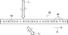
- the ejection pupil can be enlarged by diffracting a part of the light at a plurality of places of the intermediate diffraction element. can.
- each of the intermediate diffraction element 20 and the exit diffraction element 24 can enlarge the exit pupil.
- the intermediate diffraction element 20 can expand the exit pupil in the left-right direction
- the exit diffraction element 24 can expand the exit pupil in the vertical direction.
- the light guide element further diffracts light in a wavelength range different from the wavelength of the light diffracted by the incident diffraction element and the exit diffraction element. It may have an element.
- FIG. 5 shows an image display device having another example of the optical element of the present invention.
- the image display device 10c shown in FIG. 5 is a light guide element 14c having a display element 12, a light guide plate 16, an incident diffraction element 18, an exit diffraction element 24, a second incident diffraction element 19, and a second exit diffraction element 25.
- an optical element 13c having a reflecting lens 26. Since the image display device 10c has the same configuration as the image display device 10 shown in FIG. 1 except that the light guide element has the incident diffraction element 18 and the exit diffraction element 24, the following description is mainly different. conduct.
- the second incident diffraction element 19 is arranged on the main surface of the light guide plate 16 so as to be superimposed on the incident diffraction element 18.
- the second emission diffraction element 25 is arranged on the main surface of the light guide plate 16 opposite to the main surface on which the emission diffraction element 24 is arranged.
- the second emission diffraction element 25 is arranged at a position where it overlaps with the emission diffraction element 24 in the plane direction.
- the incident diffraction element 18, the exit diffraction element 24, the second incident diffraction element 19, and the second exit diffraction element 25 have wavelength selectivity for selectively diffracting light in a specific wavelength range.
- the wavelength of the light diffracted by the incident diffraction element 18 and the exit diffraction element 24 is different from the wavelength of the light diffracted by the second incident diffraction element 19 and the second exit diffraction element 25.
- the wavelength of the light diffracted by the incident diffracting element 18 and the outgoing diffracting element 24 is also referred to as a first wavelength
- the wavelength of the light diffracted by the second incident diffracting element 19 and the second outgoing diffractive element 25 is also referred to as a second wavelength.
- examples of the diffraction element having wavelength selectivity include a polarization diffraction element using a cholesteric liquid crystal layer.
- the second incident diffraction element diffracts the incident light of the second wavelength and causes it to enter the light guide plate 16.
- the second emission diffraction element emits light of the second wavelength propagating in the light guide plate 16 from the light guide plate 16, and is in a direction opposite to the emission direction of the light of the first wavelength by the emission diffraction element 24. To emit light of a second wavelength.
- the display element 12 is arranged at a position overlapping the incident diffraction element 18 and the second incident diffraction element 19 when viewed from a direction perpendicular to the main surface of the light guide plate 16.
- the display element 12 irradiates an image with light of the first wavelength diffracted by the incident diffraction element 18 and an image with light of the second wavelength diffracted by the second incident diffraction element 19.
- the display element 12 may simultaneously irradiate the image of the light of the first wavelength and the image of the light of the second wavelength, or may irradiate the image alternately.
- the configuration may include a display element that irradiates an image with light of the first wavelength and a display element that irradiates an image with light of the second wavelength.
- the display element 12 emits an image with a first wavelength and an image with a second wavelength toward the incident diffraction element 18 and the second incident diffraction element 19.
- the incident diffraction element 18 diffracts the light of the first wavelength of the incident light at an angle that totally reflects the inside of the light guide plate 16 and causes the light to enter the light guide plate 16.
- the incident diffraction element 18 diffracts the light in the direction in which the traveling direction of the diffracted light is toward the exit diffraction element 24.
- the diffracted light of the first wavelength by the incident diffraction element 18 is totally reflected in the light guide plate 16 and propagated, and is incident on the exit diffraction element 24.
- the emission diffraction element 24 diffracts the incident light of the first wavelength so as to deviate from the angle totally reflected inside the light guide plate 16. That is, as shown in FIG. 5, the exit diffraction element 24 diffracts the incident light of the first wavelength in a direction substantially perpendicular to the main surface of the light guide plate 16.
- the light of the first wavelength is incident on the second emission diffraction element 25
- the light of the first wavelength is not diffracted by the second emission diffraction element 25 and is totally reflected in the light guide plate 16.
- the light of the first wavelength diffracted by the exit diffraction element 24 is emitted from the light guide plate 16 and incident on the reflecting lens 26.
- the reflective lens 26 reflects and condenses the incident light of the first wavelength, and forms an image in the air.
- the light formed in the air is observed by the user U as an aerial image.
- the second incident diffraction element 19 diffracts the light of the second wavelength of the incident light at an angle that totally reflects the inside of the light guide plate 16 and causes the light to enter the light guide plate 16. At that time, the second incident diffraction element 19 diffracts the light in the direction in which the traveling direction of the diffracted light is toward the second exit diffraction element 25.
- the diffracted light of the second wavelength by the second incident diffraction element 19 is totally reflected in the light guide plate 16 and propagated, and is incident on the second exit diffraction element 25.
- the second emission diffraction element 25 diffracts the incident light of the second wavelength so as to deviate from the angle totally reflected inside the light guide plate 16. That is, as shown in FIG. 5, the second emitting diffraction element 25 diffracts the incident light of the second wavelength in a direction substantially perpendicular to the main surface of the light guide plate 16. Further, the second emission diffraction element 25 emits light in the direction opposite to the direction in which the light is emitted by the emission diffraction element 24, that is, in the direction opposite to the side on which the reflection lens 26 is arranged. Further, even if the light of the second wavelength is incident on the exit diffraction element 24, the light of the second wavelength is not diffracted by the exit diffraction element 24 and is totally reflected in the light guide plate 16.
- the light of the second wavelength diffracted by the second exit diffraction element 25 is emitted from the light guide plate 16 and observed by the user U.
- the image of the light of the second wavelength diffracted by the second emission diffraction element 25 is an image of the back side (infinity) of the light guide plate 16 to the user U (hereinafter, also referred to as a rear virtual image). Is recognized as. Therefore, the image display device 10c can display an aerial image displayed on the front side of the light guide plate 16 and a rear virtual image displayed on the back side of the light guide plate 16 having different display depths.
- the light of the second wavelength that is diffracted by the second incident diffraction element enters the light guide plate, and propagates in the light guide plate is directed toward the second exit diffraction element.
- It may be configured to have a second intermediate diffraction element that diffracts. That is, an incident diffraction element, an intermediate diffraction element, and an exit diffraction element that diffract the light of the first wavelength, and a second incident diffraction element, a second intermediate diffraction element, and a second exit diffraction element that diffract the light of the second wavelength. It may be configured to have and.
- the display element 12 irradiates an image (still image or moving image) to be projected in the air.
- the display element 12 is not limited, and for example, various known displays used in the image display device can be used.
- the display element 12 is not limited, and various known display elements (display devices, projectors) used in various image display devices can be used.
- display element 12 a display element having a display and a projection lens is exemplified.
- the display is not limited, and for example, various known displays used for various image display devices can be used.
- displays include liquid crystal displays (LCOS: including Liquid Crystal On Silicon), organic electroluminescence displays, and scanning display using DLP (Digital Light Processing) and MEMS (Micro Electro Mechanical Systems) mirrors. Is exemplified.
- each diffraction element has a plurality of liquid crystal layers having different selective reflection wavelengths
- a display that displays a multicolor image using light having a wavelength reflected by each liquid crystal layer is used.
- the projection lens is also a known projection lens (colimating lens) used in various image display devices.
- the display image by the display element 12 that is, the light emitted by the display element 12 is not limited, but polarized light, particularly circularly polarized light, is preferable.
- the display element 12 irradiates a circularly polarized light and the display irradiates an unpolarized image
- the display element 12 preferably has, for example, a circularly polarizing plate composed of a linear polarizing element and a ⁇ / 4 plate. ..
- the display element 12 when the display illuminates a linearly polarized image, the display element 12 preferably has, for example, a ⁇ / 4 plate.
- the light emitted by the display element 12 may be other polarized light (for example, linearly polarized light).
- the light guide plate 16 guides the incident light internally.
- the light guide plate 16 is not particularly limited, and a conventionally known light guide plate used in an image display device or the like can be used.
- the thickness of the light guide plate 16 is not particularly limited, but from the viewpoint of reducing the volume of the entire image display device, 0.01 mm to 500 mm is preferable, 0.05 mm to 100 mm is more preferable, and 0.1 mm to 10 mm is further preferable. preferable.
- the size of the main surface of the light guide plate 16 is not particularly limited, and may be appropriately set according to the size of the aerial image G1 displayed by the image display device, the size of the display surface of the display element 12, and the like.
- the incident diffraction element 18 As the incident diffraction element 18, the intermediate diffraction element 20, the exit diffraction element 24, and the second incident diffraction element 19, the second intermediate diffraction element, and the second exit diffraction element 25, conventionally known diffraction elements are appropriately used. Can be used. In the following description, when it is not necessary to distinguish the incident diffraction element 18, the intermediate diffraction element 20, the exit diffraction element 24, the second incident diffraction element 19, the second intermediate diffraction element, and the second exit diffraction element 25. Are collectively referred to as diffraction elements.
- any one of a surface relief type diffraction element, a volume hologram type diffraction element, and a polarization diffraction element is preferable.
- the polarized diffraction element is preferably a liquid crystal diffraction element formed by using a composition containing a liquid crystal compound. Further, it is also preferable that the liquid crystal diffraction element has a cholesteric liquid crystal layer in which the cholesteric liquid crystal phase is fixed. Further, the diffraction element may be a transmission type diffraction element or a reflection type diffraction element.
- the configuration of each diffraction element will be described.
- the surface relief type diffraction element As the surface relief type diffraction element, a known surface relief type diffraction element can be used. As shown in D1 illustrated in FIG. 7, the surface relief type diffraction element is configured such that fine linear irregularities are alternately arranged in parallel at a predetermined period on the surface. The period of the diffraction structure, the material, the height of the convex portion, and the like may be appropriately set according to the wavelength range to be diffracted.
- the surface relief type diffraction element may have a diffraction structure (concavo-convex structure) formed on the surface of a film-like material made of resin or the like, or a diffraction structure (concavo-convex structure) may be directly formed on the surface of the light guide plate. It may be formed.
- the concavo-convex structure formed on the surface is the diffractive structure
- the period of the concavo-convex structure is the period of the diffractive structure
- the arrangement direction of the concavo-convex structure indicated by the arrow D in FIG. 7 is the diffraction structure. It is the periodic direction.
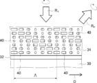
- volume hologram type diffraction element As the volume hologram type diffraction element, a known volume hologram type diffraction element can be used. As shown in D2 illustrated in FIG. 8, the volume hologram type diffraction element is configured such that a linear region 110 having a high refractive index and a linear region 112 having a low refractive index are alternately arranged in parallel at a predetermined period. It is a thing. The period of the diffraction structure, the material, the refractive index of each region, and the like may be appropriately set according to the wavelength range to be diffracted.
- the structure in which the linear region 110 having a high refractive index and the linear region 112 having a low refractive index are alternately formed is a diffraction structure, and the period of the arrangement of the region 110 and the region 112 is It is the period of the diffraction structure, and the arrangement direction of the region 110 and the region 112 shown by the arrow D in FIG. 8 is the periodic direction of the diffraction structure.
- the polarized light diffracting element is a diffracting element that controls the diffraction direction, the polarization state, and the diffracted light intensity of the emitted light according to the polarization state of the incident light by controlling the polarization state in a fine region.
- a polarized diffraction element for example, the structural double refraction described in "Erez Hasman et al., Polarization dependent focusing lens by use of quantized Pancharatnm-Berry phase diffractive optics, Applied Physics Letters, Volume 82, Number 3 pp.328-330"
- Examples thereof include a polarized diffraction element having a diffraction structure formed by using the same, a polarized diffraction element having a diffraction structure formed by using the compound refraction material described in Patent No. 5276847, and the like.
- the polarization diffraction element is formed by using a composition containing a liquid crystal compound, and has a liquid crystal orientation pattern in which the direction of the optical axis derived from the liquid crystal compound changes while continuously rotating along at least one direction in the plane.
- a liquid crystal diffraction element having a liquid crystal layer having the liquid crystal layer.
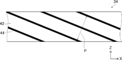
- FIG. 9 is a plan view of the cholesteric liquid crystal layer included in the reflective liquid crystal diffraction element.
- FIG. 10 is a diagram schematically showing an example of a reflective liquid crystal diffraction element.
- the reflective liquid crystal diffractive element shown in FIGS. 9 and 10 has a fixed cholesteric liquid crystal phase, and the orientation of the optical axis derived from the liquid crystal compound changes while continuously rotating along at least one direction in the plane. It has a cholesteric liquid crystal layer 34 having a liquid crystal orientation pattern.
- the cholesteric liquid crystal layer reflects one circularly polarized light of the selective reflection wavelength and transmits light in the other wavelength range and the other circularly polarized light. Therefore, the diffraction element having the cholesteric liquid crystal layer is a reflection type diffraction element.
- the reflective liquid crystal diffraction element has a support 30, an alignment film 32, and a cholesteric liquid crystal layer 34.
- the reflective liquid crystal diffraction element of the example shown in FIG. 10 has a support 30, an alignment film 32, and a cholesteric liquid crystal layer 34, but the present invention is not limited thereto.
- the reflective liquid crystal diffraction element may have, for example, only the alignment film 32 and the cholesteric liquid crystal layer 34 from which the support 30 has been peeled off after being attached to the light guide plate 16.
- the reflective liquid crystal diffraction element may have, for example, only a cholesteric liquid crystal layer 34 in which the support 30 and the alignment film 32 are peeled off after being attached to the light guide plate 16.
- the support 30 supports the alignment film 32 and the cholesteric liquid crystal layer 34.
- various sheet-like materials film, plate-like material
- the support 30 has a transmittance of 50% or more, more preferably 70% or more, and further preferably 85% or more with respect to the corresponding light.
- the thickness of the support 30 is not limited, and the thickness capable of holding the alignment film 32 and the cholesteric liquid crystal layer 34 is appropriately set according to the application of the reflective liquid crystal diffraction element, the forming material of the support 30, and the like. do it.
- the thickness of the support 30 is preferably 1 to 2000 ⁇ m, more preferably 3 to 500 ⁇ m, and even more preferably 5 to 250 ⁇ m.
- the support 30 may be single-layered or multi-layered.
- Examples of the support 30 in the case of a single layer include a support 30 made of glass, triacetyl cellulose (TAC), polyethylene terephthalate (PET), polycarbonate, polyvinyl chloride, acrylic, polyolefin, and the like.
- Examples of the support 30 in the case of a multi-layer structure include those including any of the above-mentioned single-layer supports as a substrate and providing another layer on the surface of the substrate.
- an alignment film 32 is formed on the surface of the support 30.
- the alignment film 32 is an alignment film for orienting the liquid crystal compound 40 in a predetermined liquid crystal alignment pattern when forming the cholesteric liquid crystal layer 34.
- the orientation of the optical axis 40A (see FIG. 9) derived from the liquid crystal compound 40 changes while continuously rotating along one direction in the plane. It has a liquid crystal orientation pattern. Therefore, the alignment film 32 is formed so that the cholesteric liquid crystal layer 34 can form this liquid crystal alignment pattern.
- “the direction of the optic axis 40A rotates” is also simply referred to as "the optical axis 40A rotates”.
- a rubbing-treated film made of an organic compound such as a polymer, an oblique vapor-deposited film of an inorganic compound, a film having a microgroove, and Langmuir of an organic compound such as ⁇ -tricosanoic acid, dioctadecylmethylammonium chloride and methyl stearylate examples thereof include a membrane obtained by accumulating LB (Langmuir-Blodgett) membranes produced by the Brodget method.
- the alignment film 32 by the rubbing treatment can be formed by rubbing the surface of the polymer layer with paper or cloth several times in a certain direction.
- Materials used for the alignment film 32 include polyimide, polyvinyl alcohol, polymers having a polymerizable group described in JP-A-9-152509, JP-A-2005-97377, JP-A-2005-99228, and JP-A-2005-99228. , JP-A-2005-128503, the material used for forming the alignment film 32 and the like described in JP-A-2005-128503 is preferable.
- a so-called photo-alignment film 32 which is obtained by irradiating a photo-alignable material with polarized light or non-polarized light to form the alignment film 32, is preferably used as the alignment film 32. That is, in the reflective liquid crystal diffraction element, as the alignment film 32, a photoalignment film formed by applying a photoalignment material on the support 30 is preferably used. Polarized light irradiation can be performed from a vertical direction or an oblique direction with respect to the photoalignment film, and non-polarized light irradiation can be performed from an oblique direction with respect to the photoalignment film.
- Examples of the photoalignment material used for the alignment film that can be used in the present invention include JP-A-2006-285197, JP-A-2007-76839, JP-A-2007-138138, and JP-A-2007-94071. , JP-A-2007-121721, JP-A-2007-140465, JP-A-2007-156439, JP-A-2007-133184, JP-A-2009-109831, Patent No. 3883848 and Patent No. 4151746.
- the azo compound described in JP-A the aromatic ester compound described in JP-A-2002-229039, the maleimide having the photoorientation unit described in JP-A-2002-265541 and JP-A-2002-317013, and / Alternatively, an alkenyl-substituted nadiimide compound, a photobridgeable silane derivative described in Japanese Patent No. 4205195 and Japanese Patent No. 4205198, a photocrossbable property described in Japanese Patent Application Laid-Open No. 2003-520878, Japanese Patent Application Laid-Open No. 2004-522220, and Japanese Patent No. 4162850.
- Photodimerizable compounds described in Japanese Patent Application Laid-Open No. -177561 and Japanese Patent Application Laid-Open No. 2014-12823, particularly cinnamate compounds, chalcone compounds, coumarin compounds and the like are exemplified as preferable examples.
- azo compounds, photocrosslinkable polyimides, photocrosslinkable polyamides, photocrosslinkable polyesters, synnamate compounds, and chalcone compounds are preferably used.
- the thickness of the alignment film 32 is not limited, and the thickness at which the required alignment function can be obtained may be appropriately set according to the material for forming the alignment film 32.
- the thickness of the alignment film 32 is preferably 0.01 to 5 ⁇ m, more preferably 0.05 to 2 ⁇ m.
- the method for forming the alignment film 32 there is no limitation on the method for forming the alignment film 32, and various known methods depending on the material for forming the alignment film 32 can be used. As an example, a method in which the alignment film 32 is applied to the surface of the support 30 and dried, and then the alignment film 32 is exposed with a laser beam to form an alignment pattern is exemplified.
- FIG. 16 conceptually shows an example of an exposure apparatus that exposes the alignment film 32 to form an alignment pattern.
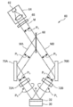
- the exposure apparatus 60 shown in FIG. 16 uses a light source 64 provided with a laser 62, a ⁇ / 2 plate 65 for changing the polarization direction of the laser beam M emitted by the laser 62, and a light beam MA and the laser beam M emitted by the laser 62. It includes a polarizing beam splitter 68 that separates the MB into two, mirrors 70A and 70B arranged on the optical paths of the two separated rays MA and MB, respectively, and ⁇ / 4 plates 72A and 72B.
- the light source 64 emits linearly polarized light P 0 .
- lambda / 4 plate 72A is linearly polarized light P 0 (the ray MA) to the right circularly polarized light P R
- lambda / 4 plate 72B is linearly polarized light P 0 (the rays MB) to the left circularly polarized light P L, converts respectively.
- a support 30 having the alignment film 32 before the alignment pattern is formed is arranged in the exposed portion, and the two light rays MA and the light rays MB are crossed and interfered with each other on the alignment film 32, and the interference light is made to interfere with the alignment film 32. Is exposed to light. Due to the interference at this time, the polarization state of the light applied to the alignment film 32 periodically changes in the form of interference fringes. As a result, an alignment film having an orientation pattern in which the orientation state changes periodically (hereinafter, also referred to as a pattern alignment film) can be obtained.
- the period of the orientation pattern can be adjusted by changing the intersection angle ⁇ of the two rays MA and MB. That is, in the exposure apparatus 60, in an orientation pattern in which the optical axis 40A derived from the liquid crystal compound 40 continuously rotates along one direction by adjusting the crossing angle ⁇ , the optical axis 40A rotates in one direction. , The length of one cycle in which the optic axis 40A rotates 180 ° can be adjusted.
- the optical axis 40A derived from the liquid crystal compound 40 is aligned along one direction, as will be described later.
- the cholesteric liquid crystal layer 34 having a continuously rotating liquid crystal orientation pattern can be formed. Further, the rotation direction of the optical shaft 40A can be reversed by rotating the optical axes of the ⁇ / 4 plates 72A and 72B by 90 °, respectively.
- the direction of the optical axis of the liquid crystal compound in the cholesteric liquid crystal layer formed on the pattern alignment film changes while continuously rotating along at least one direction in the plane. It has an orientation pattern that orients the liquid crystal compound so that it becomes a liquid crystal alignment pattern.
- the axis of the pattern alignment film is the axis along the direction in which the liquid crystal compound is oriented
- the direction of the alignment axis of the pattern alignment film changes while continuously rotating along at least one direction in the plane. It can be said that it has an orientation pattern.
- the orientation axis of the pattern alignment film can be detected by measuring the absorption anisotropy. For example, when the pattern alignment film is irradiated with rotating linearly polarized light and the amount of light transmitted through the pattern alignment film is measured, the direction in which the amount of light becomes maximum or minimum gradually changes along one direction in the plane. It changes and is observed.
- the alignment film 32 is provided as a preferred embodiment and is not an essential constituent requirement.
- the cholesteric liquid crystal layer 34 is made of optics derived from the liquid crystal compound 40. It is also possible to have a configuration having a liquid crystal orientation pattern in which the orientation of the axis 40A changes while continuously rotating along at least one direction in the plane. That is, in the present invention, the support 30 may act as an alignment film.
- the cholesteric liquid crystal layer 34 is formed on the surface of the alignment film 32.
- the cholesteric liquid crystal layer is a cholesteric liquid crystal layer in which the cholesteric liquid crystal phase is fixed, and the direction of the optic axis derived from the liquid crystal compound changes while continuously rotating along at least one direction in the plane. It is a cholesteric liquid crystal layer having a liquid crystal orientation pattern.
- a cholesteric liquid crystal layer having a liquid crystal orientation pattern in which the orientation of the optic axis derived from the liquid crystal compound changes while continuously rotating along at least one direction in the plane is SEM in a cross section perpendicular to the main surface of the cholesteric liquid crystal layer.
- the arrangement direction of the bright part and the dark part derived from the cholesteric liquid crystal phase observed in 1 is inclined with respect to the main surface of the cholesteric liquid crystal layer.
- the cholesteric liquid crystal layer 34 has a spiral structure in which liquid crystal compounds 40 are spirally swirled and stacked, similar to the cholesteric liquid crystal layer formed by fixing a normal cholesteric liquid crystal phase.
- the liquid crystal compound 40 which is spirally swirled, has a structure in which the liquid crystal compounds 40 are stacked at a plurality of pitches, with the configuration in which the liquid crystal compounds 40 are spirally rotated once (rotated 360 °) and stacked as one spiral pitch.
- the cholesteric liquid crystal layer in which the cholesteric liquid crystal phase is fixed has wavelength selective reflectivity.
- the selective reflection wavelength range of the cholesteric liquid crystal layer depends on the length of the spiral 1 pitch in the thickness direction described above.
- the spiral pitch substantially coincides with the inclined surface pitch P shown in FIG.
- the spiral pitch deviates slightly from the inclined surface pitch P shown in FIG. 11, but in the following description, the spiral pitch The explanation will be given without distinguishing between the pitch and the pitch of the inclined surface.
- the pitch P of the cholesteric liquid crystal layer is adjusted for each liquid crystal diffraction element to make the cholesteric.
- the selective reflection wavelength range of the liquid crystal layer may be appropriately set.
- the liquid crystal compounds 40 are arranged along a plurality of array axes D parallel to each other in the XY plane, and the respective array axes D.
- the orientation of the optic axis 40A of the liquid crystal compound 40 changes while continuously rotating in one direction in the plane along the array axis D.
- the array axis D is oriented in the X direction.
- the liquid crystal compounds 40 having the same orientation of the optical axis 40A are oriented at equal intervals.
- the direction of the optical axis 40A of the liquid crystal compound 40 changes while continuously rotating in one direction in the plane along the array axis D
- the optical axis 40A and the array axis D of the liquid crystal compound 40 change.
- the angle formed by the optic axis D differs depending on the position in the direction of the array axis D, and the angle formed by the optic axis 40A and the array axis D gradually changes from ⁇ to ⁇ + 180 ° or ⁇ -180 ° along the array axis D. It means that you are. That is, as shown in FIG. 3, the plurality of liquid crystal compounds 40 arranged along the array axis D change while the optical axis 40A rotates by a constant angle along the array axis D.
- the difference in angle between the optical axes 40A of the liquid crystal compounds 40 adjacent to each other in the array axis D direction is preferably 45 ° or less, more preferably 15 ° or less, and further preferably a smaller angle. preferable.
- the optical axis 40A of the liquid crystal compound 40 is intended to be the molecular major axis of the rod-shaped liquid crystal compound.
- the optical axis 40A of the liquid crystal compound 40 is intended to be an axis parallel to the normal direction of the disk-shaped liquid crystal compound with respect to the disk surface.
- the optical axis 40A of the liquid crystal compound 40 is 180 ° in the arrangement axis D direction in which the optical axis 40A continuously rotates and changes in the plane.
- the length (distance) of rotation be the length ⁇ of one cycle in the liquid crystal alignment pattern. That is, the distance between the centers of the two liquid crystal compounds 40 having the same angle with respect to the array axis D direction in the array axis D direction is defined as the length ⁇ of one cycle.
- the distance between the centers of the two liquid crystal compounds 40 in which the direction of the arrangement axis D and the direction of the optical axis 40A coincide with each other in the direction of the arrangement axis D is the length of one cycle ⁇ . And. In the following description, the length ⁇ of this one cycle is also referred to as "one cycle ⁇ ".
- the liquid crystal orientation pattern of the cholesteric liquid crystal layer 34 repeats this one cycle ⁇ in one direction in which the direction of the array axis D, that is, the direction of the optic axis 40A is continuously rotated and changed.
- the liquid crystal compound 40 forming the cholesteric liquid crystal layer 34 is in the direction orthogonal to the arrangement axis D direction (Y direction in FIG. 9), that is, in the Y direction orthogonal to one direction in which the optical axis 40A continuously rotates.
- the directions of the optical axes 40A are equal.
- the liquid crystal compound 40 forming the cholesteric liquid crystal layer 34 has the same angle formed by the optical axis 40A of the liquid crystal compound 40 and the arrangement axis D direction in the Y direction.
- the arrangement direction in which the bright portions 42 and the dark portions 44 are alternately arranged as shown in FIG. 11 is the main.
- a striped pattern that is inclined at a predetermined angle with respect to the plane (XY plane) is observed.
- the distance between the adjacent bright portion 42 to the bright portion 42 or the dark portion 44 to the dark portion 44 in the normal direction of the line formed by the bright portion 42 or the dark portion 44 corresponds to 1/2 pitch.
- the spiral axis derived from the cholesteric liquid crystal phase is perpendicular to the main surface (XY plane), and its reflecting surface is a plane parallel to the main surface (XY plane).
- the optical axis of the liquid crystal compound is not inclined with respect to the main surface (XY plane).
- the optic axis is parallel to the main plane (XY plane). Therefore, when the XX plane of the conventional cholesteric liquid crystal layer is observed by SEM, the arrangement direction in which the bright portion and the dark portion are alternately arranged is perpendicular to the main plane (XY plane). Since the cholesteric liquid crystal phase is specularly reflective, for example, when light is incident on the cholesteric liquid crystal layer from the normal direction, the light is reflected in the normal direction.
- the cholesteric liquid crystal layer 34 having a configuration in which the arrangement directions of the bright part and the dark part are inclined reflects the incident light by tilting it in the arrangement axis D direction with respect to specular reflection.
- the cholesteric liquid crystal layer 34 has a liquid crystal orientation pattern in which the optical axis 40A changes while continuously rotating along the arrangement axis D direction (a predetermined one direction) in the plane.
- the cholesteric liquid crystal layer 34 is a cholesteric liquid crystal layer that selectively reflects the right-handed circularly polarized light R R of red light. Therefore, when light is incident on the cholesteric liquid crystal layer 34, the cholesteric liquid crystal layer 34 reflects only right circularly polarized light R R of the red light, and transmits light of other wavelengths.
- the optical axis 40A of the liquid crystal compound 40 changes while rotating along the array axis D direction (one direction).
- the liquid crystal orientation pattern formed on the cholesteric liquid crystal layer 34 is a periodic pattern in the arrangement axis D direction. Therefore, the right circularly polarized light R R of the red light incident on the cholesteric liquid crystal layer 34, as shown conceptually in FIG 12, is reflected (diffracted) in the direction corresponding to the period of the liquid crystal orientation pattern, reflected red right circularly polarized light R R of the light is reflected (diffracted) in a direction inclined to the array axis direction D with respect to the XY plane (major surface of the cholesteric liquid crystal layer).
- the light reflection direction (diffraction angle) can be adjusted by appropriately setting the array axis D direction, which is one direction in which the optic axis 40A rotates.
- the reflection direction of the circularly polarized light can be reversed by reversing the rotation direction of the optical axis 40A of the liquid crystal compound 40 toward the array axis D direction. ..
- the rotation direction of the optical axis 40A toward the arrangement axis D direction is clockwise, and a certain circularly polarized light is reflected by tilting it in the arrangement axis D direction, which is counterclockwise.
- a certain circularly polarized light is reflected by tilting in the direction opposite to the direction of the array axis D.
- the reflection direction is reversed depending on the spiral turning direction of the liquid crystal compound 40, that is, the turning direction of the reflected circularly polarized light.
- the spiral turning direction of the liquid crystal compound 40 that is, the turning direction of the reflected circularly polarized light.
- the optical axis 40A has a liquid crystal alignment pattern that rotates clockwise along the arrangement axis D direction to the right. Circularly polarized light is reflected by tilting it in the direction of the array axis D.
- the liquid crystal layer has a liquid crystal orientation pattern in which the optical axis 40A rotates clockwise along the arrangement axis D direction. Reflects the left circularly polarized light tilted in the direction opposite to the arrangement axis D direction.
- the shorter one cycle ⁇ is, the larger the angle of the reflected light with respect to the incident light is. That is, the shorter one cycle ⁇ is, the more the reflected light can be tilted and reflected with respect to the incident light. Therefore, one cycle of the liquid crystal alignment pattern in the liquid crystal layer of each diffraction element may be appropriately set according to the diffraction angle, arrangement, and the like of each diffraction element.
- the period (1 period ⁇ ) of the diffraction structure of these diffraction elements is preferably 0.1 ⁇ m to 10 ⁇ m, more preferably 0.1 ⁇ m to 1 ⁇ m, further preferably 0.1 ⁇ m to 0.8 ⁇ m, and propagates through the light guide plate by total reflection. From the viewpoint of causing the light to occur, it is more preferable that the wavelength of the incident light is ⁇ or less.
- the liquid crystal compound 40 in the XX plane of the cholesteric liquid crystal layer 34, has an optical axis 40A oriented parallel to the main plane (XY plane).
- the liquid crystal compound 40 is oriented with its optical axis 40A inclined with respect to the main plane (XY plane). It may be.
- the inclination angle (tilt angle) with respect to the main plane (XY plane) of the liquid crystal compound 40 is uniform in the thickness direction (Z direction).
- the cholesteric liquid crystal layer 34 may have regions in which the tilt angles of the liquid crystal compounds 40 differ in the thickness direction.
- the optical axis 40A of the liquid crystal compound 40 is parallel to the main surface (the pretilt angle is 0) at the interface on the alignment film 32 side of the cholesteric liquid crystal layer, and the interface on the alignment film 32 side.
- the tilt angle of the liquid crystal compound 40 increases as the distance from the liquid crystal compound 40 increases in the thickness direction, and then the liquid crystal compound is oriented at a constant tilt angle to the other interface (air interface) side.
- the cholesteric liquid crystal layer may have a configuration in which the optical axis of the liquid crystal compound has a pretilt angle at one interface of the upper and lower interfaces, and has a configuration having a pretilt angle at both interfaces. May be good. Further, the pretilt angle may be different at both interfaces. Since the liquid crystal compound has a tilt angle (tilt) in this way, the birefringence of the liquid crystal compound that is effective when light is diffracted becomes high, and the diffraction efficiency can be improved.
- the average angle (average tilt angle) formed by the optical axis 40A of the liquid crystal compound 40 and the main surface (XY plane) is preferably 5 to 80 °, more preferably 10 to 50 °.
- the average tilt angle can be measured by observing the XX plane of the cholesteric liquid crystal layer 34 with a polarizing microscope. Above all, in the XX plane of the cholesteric liquid crystal layer 34, it is preferable that the optical axis 40A of the liquid crystal compound 40 is inclined or oriented in the same direction with respect to the main plane (XY plane).
- the tilt angle is a value obtained by measuring the angle formed by the optical axis 40A of the liquid crystal compound 40 and the main surface at any five or more points in the polarization microscope observation of the cross section of the cholesteric liquid crystal layer and arithmetically averaging them. be.
- cholesteric liquid crystal layer Light vertically incident on the diffraction element (cholesteric liquid crystal layer) travels diagonally in the cholesteric liquid crystal layer with a bending force applied.
- a diffraction loss occurs because a deviation from conditions such as a diffraction period originally set so as to obtain a desired diffraction angle with respect to vertical incidence occurs.
- the liquid crystal compound is tilted, there is an orientation in which a higher birefringence is generated with respect to the orientation in which the light is diffracted, as compared with the case where the liquid crystal compound is not tilted.
- the effective abnormal light refractive index becomes large, so that the double refractive index, which is the difference between the abnormal light refractive index and the normal light refractive index, becomes high.
- the direction of the tilt angle according to the target diffraction direction, it is possible to suppress the deviation from the original diffraction condition in that direction, and as a result, a liquid crystal compound having a tilt angle was used. In this case, it is considered that higher diffraction efficiency can be obtained.
- the tilt angle is controlled by the treatment of the interface of the liquid crystal layer.
- the tilt angle of the liquid crystal compound can be controlled by performing a pre-tilt treatment on the alignment film. For example, when the alignment film is formed by exposing the alignment film to ultraviolet rays from the front and then diagonally exposing the alignment film, a pretilt angle can be generated in the liquid crystal compound in the cholesteric liquid crystal layer formed on the alignment film. In this case, the liquid crystal compound is pre-tilted in a direction in which the uniaxial side of the liquid crystal compound can be seen with respect to the second irradiation direction.
- liquid crystal compound in the direction perpendicular to the second irradiation direction does not pre-tilt, there are an in-plane pre-tilt region and a non-pre-tilt region. This is suitable for increasing the diffraction efficiency because it contributes to the highest birefringence in that direction when the light is diffracted in the target direction.
- an additive that promotes the pretilt angle can be added in the cholesteric liquid crystal layer or the alignment film. In this case, an additive can be used as a factor for further increasing the diffraction efficiency. This additive can also be used to control the pretilt angle of the interface on the air side.
- the cholesteric liquid crystal layer is in-plane retardation in either the slow phase axis plane or the phase advance axis plane.
- the direction in which Re is minimized is inclined from the normal direction.
- the absolute value of the measurement angle formed by the normal in the direction in which the in-plane retardation Re is minimized is 5 ° or more.
- the liquid crystal compound of the cholesteric liquid crystal layer is inclined with respect to the main surface, and the inclination direction substantially coincides with the bright part and the dark part of the cholesteric liquid crystal layer.
- the normal direction is a direction perpendicular to the main surface. Since the cholesteric liquid crystal layer has such a configuration, circularly polarized light can be diffracted with higher diffraction efficiency as compared with the cholesteric liquid crystal layer in which the liquid crystal compound is parallel to the main surface.
- the liquid crystal compound of the cholesteric liquid crystal layer is inclined with respect to the main surface and the inclination direction substantially coincides with the bright part and the dark part
- the bright part and the dark part corresponding to the reflecting surface and the optical axis of the liquid crystal compound are used.
- the action of the liquid crystal compound on the reflection (diffraction) of light is increased, and the diffraction efficiency can be improved.
- the amount of reflected light with respect to the incident light can be further improved.
- the absolute value of the optical axis tilt angle of the cholesteric liquid crystal layer is preferably 5 ° or more, more preferably 15 ° or more, still more preferably 20 ° or more.
- the absolute value of the optical axis tilt angle is preferably 5 ° or more, more preferably 15 ° or more, still more preferably 20 ° or more.
- the shape of the light-dark line composed of the bright portion 42 and the dark portion 44 derived from the cholesteric liquid crystal phase observed by SEM on the XX plane is wavy (wavy structure). It is also possible to use the cholesteric liquid crystal layer of. Since the cholesteric liquid crystal layer having a wavy light and dark line shape can diffuse light, the viewing angle of the image displayed in the projection type image display system can be increased.
- the cholesteric liquid crystal layer shown in FIG. 15 has the same configuration as the cholesteric liquid crystal layer shown in FIG. 11 except that the shape of the light-dark line composed of the bright portion 42 and the dark portion 44 is wavy. That is, the cholesteric liquid crystal layer shown in FIG. 15 is a layer having a cholesteric liquid crystal structure and having a structure in which the angle formed by the spiral axis and the surface of the reflective layer changes periodically. In other words, the cholesteric liquid crystal layer has a cholesteric liquid crystal structure, and the cholesteric liquid crystal structure gives a striped pattern of bright and dark parts in the cross-sectional view observed by SEM, and the normal and reflective layers of the lines formed by the dark parts. It is a layer in which the angle formed with the surface changes periodically.
- the wavy structure means that at least one region M in which the absolute value of the inclination angle with respect to the plane of the cholesteric liquid crystal layer is 5 ° or more exists in the continuous line of the bright or dark portion forming the striped pattern, and the region It is a structure in which peaks or valleys with an inclination angle of 0 ° are specified at the positions closest to each other with M in the plane direction.
- a peak or valley having an inclination angle of 0 ° includes convex and concave points, but if the inclination angle is 0 °, it also includes steps and shelves.
- a region M in which the absolute value of the inclination angle is 5 ° or more and a mountain or a valley sandwiching the region M are repeated in a plurality of continuous lines in a bright part or a dark part of a striped pattern.
- the cholesteric liquid crystal layer having a wavy structure can be formed by forming the cholesteric liquid crystal layer on a forming surface that is not subjected to an orientation treatment such as rubbing.
- the cholesteric liquid crystal layer can be formed by fixing the cholesteric liquid crystal phase in a layered manner.
- the structure in which the cholesteric liquid crystal phase is fixed may be a structure in which the orientation of the liquid crystal compound that is the cholesteric liquid crystal phase is maintained, and typically, the polymerizable liquid crystal compound is placed in the orientation state of the cholesteric liquid crystal phase. Therefore, it is preferable that the structure is polymerized and cured by irradiation with ultraviolet rays, heating, etc. to form a non-fluid layer, and at the same time, the structure is changed to a state in which the orientation form is not changed by an external field or an external force.
- the polymerizable liquid crystal compound may lose its liquid crystal property by increasing its molecular weight by a curing reaction.
- a liquid crystal composition containing a liquid crystal compound can be mentioned.
- the liquid crystal compound is preferably a polymerizable liquid crystal compound.
- the liquid crystal composition used for forming the cholesteric liquid crystal layer may further contain a surfactant and a chiral agent.
- the polymerizable liquid crystal compound may be a rod-shaped liquid crystal compound or a disk-shaped liquid crystal compound.
- the rod-shaped polymerizable liquid crystal compound forming the cholesteric liquid crystal phase include a rod-shaped nematic liquid crystal compound.
- rod-shaped nematic liquid crystal compounds examples include azomethines, azoxys, cyanobiphenyls, cyanophenyl esters, benzoic acid esters, cyclohexanecarboxylic acid phenyl esters, cyanophenylcyclohexanes, cyano-substituted phenylpyrimidines, and alkoxy-substituted phenylpyrimidines.
- Phenyldioxans, trans, alkenylcyclohexylbenzonitriles and the like are preferably used. Not only low molecular weight liquid crystal compounds but also high molecular weight liquid crystal compounds can be used.
- the polymerizable liquid crystal compound is obtained by introducing a polymerizable group into the liquid crystal compound.
- the polymerizable group include an unsaturated polymerizable group, an epoxy group, and an aziridinyl group, and an unsaturated polymerizable group is preferable, and an ethylenically unsaturated polymerizable group is more preferable.
- the polymerizable group can be introduced into the molecule of the liquid crystal compound by various methods.
- the number of polymerizable groups contained in the polymerizable liquid crystal compound is preferably 1 to 6, more preferably 1 to 3.
- Examples of polymerizable liquid crystal compounds include Makromol. Chem. , 190, 2255 (1989), Advanced Materials 5, 107 (1993), US Pat. No.
- a cyclic organopolysiloxane compound having a cholesteric phase as disclosed in Japanese Patent Application Laid-Open No. 57-165480 can be used.
- a polymer liquid crystal compound a polymer having a mesogen group exhibiting a liquid crystal introduced at the main chain, a side chain, or both the main chain and the side chain, and a polymer cholesteric having a cholesteryl group introduced into the side chain.
- Liquid crystals, liquid crystal polymers as disclosed in JP-A-9-133810, liquid crystal polymers as disclosed in JP-A-11-293252, and the like can be used.
- disk-shaped liquid crystal compound As the disk-shaped liquid crystal compound, for example, those described in JP-A-2007-108732 and JP-A-2010-244038 can be preferably used.
- the amount of the polymerizable liquid crystal compound added to the liquid crystal composition is preferably 75 to 99.9% by mass, preferably 80 to 99% by mass, based on the solid content mass (mass excluding the solvent) of the liquid crystal composition. It is more preferably mass%, and even more preferably 85-90 mass%.
- the liquid crystal composition used for forming the cholesteric liquid crystal layer may contain a surfactant.
- the surfactant is preferably a compound capable of stably or rapidly functioning as an orientation control agent that contributes to the orientation of the cholesteric liquid crystal phase.
- examples of the surfactant include silicone-based surfactants and fluorine-based surfactants, and fluorine-based surfactants are preferably exemplified.
- the surfactant include the compounds described in paragraphs [2002] to [0090] of JP2014-119605A, and the compounds described in paragraphs [0031] to [0034] of JP2012-203237A. , The compounds exemplified in paragraphs [0092] and [093] of JP-A-2005-999248, paragraphs [0076] to [0078] and paragraphs [0083] to [0085] of JP-A-2002-129162. Examples thereof include the compounds exemplified therein, and the fluorine (meth) acrylate-based polymers described in paragraphs [0018] to [0043] of JP-A-2007-272185.
- the surfactant one type may be used alone, or two or more types may be used in combination.
- the fluorine-based surfactant the compounds described in paragraphs [2002] to [0090] of JP-A-2014-119605 are preferable.
- the amount of the surfactant added to the liquid crystal composition is preferably 0.01 to 10% by mass, more preferably 0.01 to 5% by mass, and 0.02 to 1% by mass with respect to the total mass of the liquid crystal compound. Is even more preferable.
- the chiral agent has a function of inducing a helical structure of a cholesteric liquid crystal phase. Since the twist direction or spiral pitch of the spiral induced by the compound differs depending on the compound, the chiral agent may be selected according to the purpose.
- the chiral agent is not particularly limited, and is a known compound (for example, Liquid Crystal Device Handbook, Chapter 3, Section 4-3, TN (twisted nematic), STN (Super Twisted Nematic) chiral agent, page 199, Japan Society for the Promotion of Science. (Described in 1989, edited by the 142nd Committee of the Society), isosorbide, isomannide derivatives and the like can be used.
- the chiral agent generally contains an asymmetric carbon atom, but an axial asymmetric compound or a surface asymmetric compound that does not contain an asymmetric carbon atom can also be used as the chiral agent.
- axial or surface asymmetric compounds include binaphthyl, helicene, paracyclophane, and derivatives thereof.
- the chiral agent may have a polymerizable group. When both the chiral agent and the liquid crystal compound have a polymerizable group, the repeating unit derived from the polymerizable liquid crystal compound and the repeating unit derived from the chiral agent are derived by the polymerization reaction between the polymerizable chiral agent and the polymerizable liquid crystal compound. Polymers with repeating units can be formed.
- the polymerizable group of the polymerizable chiral agent is preferably a group of the same type as the polymerizable group of the polymerizable liquid crystal compound. Therefore, the polymerizable group of the chiral agent is preferably an unsaturated polymerizable group, an epoxy group or an aziridinyl group, more preferably an unsaturated polymerizable group, and preferably an ethylenically unsaturated polymerizable group. More preferred. Moreover, the chiral agent may be a liquid crystal compound.
- the chiral auxiliary has a photoisomeric group
- a pattern of a desired reflection wavelength corresponding to the emission wavelength can be formed by irradiating a photomask such as an active ray after coating and orientation.
- a photomask such as an active ray after coating and orientation.
- an isomerization site of a compound exhibiting photochromic properties, an azo group, an azoxy group, or a cinnamoyl group is preferable.
- Specific compounds include JP-A-2002-80478, JP-A-2002-80851, JP-A-2002-179668, JP-A-2002-179669, JP-A-2002-179670, and JP-A-2002.
- the content of the chiral agent in the liquid crystal composition is preferably 0.01 to 200 mol%, more preferably 1 to 30 mol%, based on the molar content of the liquid crystal compound.
- the liquid crystal composition contains a polymerizable compound, it preferably contains a polymerization initiator.
- the polymerization initiator used is preferably a photopolymerization initiator capable of initiating the polymerization reaction by irradiation with ultraviolet rays.
- photopolymerization initiators include ⁇ -carbonyl compounds (described in U.S. Pat. No. 2,376,661 and U.S. Pat. No. 2,376,670), acidoin ethers (described in U.S. Pat. No. 2,448,828), and ⁇ -hydrogen.
- Substituted aromatic acidoine compounds (described in US Pat. No. 2722512), polynuclear quinone compounds (described in US Pat. Nos. 3046127 and US Pat. No. 2951758), triarylimidazole dimers and p-aminophenyl ketone. Combinations (described in US Pat. No. 3,549,677), aclysine and phenazine compounds (Japanese Patent Laid-Open No. 60-105667, described in US Pat. No. 4,239,850), and oxadiazole compounds (US Pat. No. 421,970). Description) and the like.
- the content of the photopolymerization initiator in the liquid crystal composition is preferably 0.1 to 20% by mass, more preferably 0.5 to 12% by mass, based on the content of the liquid crystal compound.
- the liquid crystal composition may optionally contain a cross-linking agent in order to improve the film strength and durability after curing.
- a cross-linking agent those that are cured by ultraviolet rays, heat, humidity and the like can be preferably used.
- the cross-linking agent is not particularly limited and may be appropriately selected depending on the intended purpose. For example, a polyfunctional acrylate compound such as trimethylolpropane tri (meth) acrylate and pentaerythritol tri (meth) acrylate; glycidyl (meth) acrylate.
- epoxy compounds such as ethylene glycol diglycidyl ether; aziridine compounds such as 2,2-bishydroxymethylbutanol-tris [3- (1-aziridinyl) propionate] and 4,4-bis (ethyleneiminocarbonylamino) diphenylmethane; hexa Isocyanate compounds such as methylenediisocyanate and biuret-type isocyanate; polyoxazoline compounds having an oxazoline group in the side chain; and alkoxysilane compounds such as vinyltrimethoxysilane and N- (2-aminoethyl) 3-aminopropyltrimethoxysilane. Can be mentioned.
- a known catalyst can be used depending on the reactivity of the cross-linking agent, and the productivity can be improved in addition to the improvement of the film strength and the durability. These may be used alone or in combination of two or more.
- the content of the cross-linking agent is preferably 3 to 20% by mass, more preferably 5 to 15% by mass, based on the solid content mass of the liquid crystal composition. When the content of the cross-linking agent is within the above range, the effect of improving the cross-linking density can be easily obtained, and the stability of the cholesteric liquid crystal phase is further improved.
- a polymerization inhibitor an antioxidant, an ultraviolet absorber, a light stabilizer, a coloring material, metal oxide fine particles, etc. are added to the liquid crystal composition within a range that does not deteriorate the optical performance and the like. Can be added with.
- the liquid crystal composition is preferably used as a liquid when forming a cholesteric liquid crystal layer.
- the liquid crystal composition may contain a solvent.
- the solvent is not limited and may be appropriately selected depending on the intended purpose, but an organic solvent is preferable.
- the organic solvent is not limited and may be appropriately selected depending on the intended purpose.
- the liquid crystal composition When forming the cholesteric liquid crystal layer, the liquid crystal composition is applied to the forming surface of the cholesteric liquid crystal layer, the liquid crystal compound is oriented in the state of the cholesteric liquid crystal phase, and then the liquid crystal compound is cured to form the cholesteric liquid crystal layer.
- the liquid crystal composition is applied to the alignment film 32, the liquid crystal compound is oriented in the state of the cholesteric liquid crystal phase, and then the liquid crystal compound is cured to form cholesteric. It is preferable to form a cholesteric liquid crystal layer in which the liquid crystal phase is fixed.
- printing methods such as inkjet and scroll printing, and known methods such as spin coating, bar coating and spray coating that can uniformly apply the liquid to a sheet-like material can be used.
- the applied liquid crystal composition is dried and / or heated as needed and then cured to form a cholesteric liquid crystal layer.
- the liquid crystal compound in the liquid crystal composition may be oriented to the cholesteric liquid crystal phase.
- the heating temperature is preferably 200 ° C. or lower, more preferably 130 ° C. or lower.
- the oriented liquid crystal compound is further polymerized, if necessary.
- the polymerization may be either thermal polymerization or photopolymerization by light irradiation, but photopolymerization is preferable.
- the irradiation energy is preferably 20mJ / cm 2 ⁇ 50J / cm 2, more preferably 50 ⁇ 1500mJ / cm 2.
- light irradiation may be carried out under heating conditions or a nitrogen atmosphere.
- the wavelength of the ultraviolet rays to be irradiated is preferably 250 to 430 nm.
- a composition containing a disk-shaped liquid crystal compound is used to form an inclined liquid crystal layer in which the molecular axis of the disk-shaped liquid crystal compound is inclined with respect to the surface, and the inclined liquid crystal layer is formed.
- a method of forming a cholesteric liquid crystal layer using a composition containing a liquid crystal compound is also preferably used.
- a method for forming a cholesteric liquid crystal layer using such a tilted liquid crystal layer is described in paragraphs [0049] to [0194] of International Publication 2019/181247.
- the thickness of the cholesteric liquid crystal layer there is no limit to the thickness of the cholesteric liquid crystal layer, and the required amount of light depends on the application of the reflective liquid crystal diffraction element, the light reflectance required for the cholesteric liquid crystal layer, the material for forming the cholesteric liquid crystal layer, and the like.
- the thickness at which the reflectance can be obtained may be appropriately set.
- each diffraction element has one liquid crystal layer having wavelength selectivity. It may have a structure having layers, or it may have a structure having two or more layers.
- the diffraction element has two or more liquid crystal layers, in each of the two or more liquid crystal layers, in the cross section of the liquid crystal layer observed by SEM, the bright part and the dark part derived from the liquid crystal phase are relative to the main surface of the liquid crystal layer. It is preferable that the pitch Ps of the liquid crystal layers are different from each other when the distance in the normal direction from the bright portion to the bright portion or from the dark portion to the inclined surface in the dark portion is set to 1/2 pitch. That is, it is preferable that the two or more liquid crystal layers have different wavelength selectivity.
- the diffractive element may have two liquid crystal layers, that is, a liquid crystal layer that selectively reflects red light and a liquid crystal layer that selectively reflects green light, and the liquid crystal layer that selectively reflects red light. It may have three liquid crystal layers, that is, a liquid crystal layer that selectively reflects green light and a liquid crystal layer that selectively reflects blue light.
- each liquid crystal layer reflects three colors of light, red light, green light, and blue light, so that the light guide element can be colored.
- the image can be guided.
- the diffractive element has three liquid crystal layers having different selective reflection center wavelengths, and has one or two colors selected from visible light such as red light, green light, and blue light, and infrared rays and / or. It may be configured to reflect ultraviolet rays, or may be configured to reflect only light other than visible light.
- the diffraction element may have two or four or more liquid crystal layers having different selective reflection center wavelengths.
- the diffractive element may be configured to reflect light other than visible light such as infrared light and / or ultraviolet light in addition to visible light such as red light, green light and blue light, or each liquid crystal layer may be composed of infrared light and light. / Or a configuration that reflects light other than visible light such as ultraviolet light may be used.
- each of the two or more liquid crystal layers has a length in which the direction of the optical axis derived from the liquid crystal compound in the liquid crystal orientation pattern rotates 180 ° in the in-plane direction, that is, diffraction. It is preferable that one cycle ⁇ of the structure is different from each other. Specifically, when the pitches P of the liquid crystal layers are different from each other, the permutation of the pitch P (length of the selective reflection center wavelength) and the permutation of the length of one cycle ⁇ in the liquid crystal orientation pattern of the liquid crystal layer are equal. Is preferable.
- each liquid crystal layer can be substantially matched, and the diffraction angles of the selective reflection wavelength of each liquid crystal layer with respect to light can be substantially matched. That is, light having different wavelengths can be diffracted in substantially the same direction.
- the pitch of the first liquid crystal layer is P1
- one cycle is ⁇ 1
- the pitch of the second liquid crystal layer is P2.
- one cycle is ⁇ 2
- the transmissive liquid crystal diffraction element has a liquid crystal orientation pattern that is continuously rotated along at least one direction in the plane, and the liquid crystal compound does not form a cholesteric liquid crystal phase in the thickness direction. It is an element.
- the liquid crystal diffraction element may have a configuration in which the liquid crystal compound is twisted and rotated in the thickness direction to the extent that the liquid crystal compound does not become a cholesteric liquid crystal phase.
- FIGS. 17 and 18 show an example of a transmissive liquid crystal diffraction grating.
- the transmissive liquid crystal diffraction element shown in FIGS. 17 and 18 includes a support 30, an alignment film 32, and a liquid crystal layer 36.
- the liquid crystal layer 36 of the transmissive liquid crystal diffraction element also has a liquid crystal orientation pattern in which the optical axis 40A of the liquid crystal compound 40 continuously rotates along the array axis D direction, similarly to the cholesteric liquid crystal layer 34.
- FIG. 18 also shows only the liquid crystal compound on the surface of the alignment film 32, as in FIG. 9 described above.
- the liquid crystal compound 40 forming the liquid crystal layer 36 is not spirally twisted and rotated in the thickness direction, and the optic axis 40A is located at the same position in the plane direction.
- Such a liquid crystal layer can be formed by not adding a chiral agent to the liquid crystal composition in the formation of the cholesteric liquid crystal layer described above.
- the liquid crystal layer 36 has a liquid crystal orientation pattern in which the orientation of the optical axis 40A derived from the liquid crystal compound 40 changes while continuously rotating along the array axis D direction.
- the liquid crystal compound 40 forming the liquid crystal layer 36 has the same orientation of the optical axes 40A in the Y direction orthogonal to the arrangement axis D direction, that is, in the Y direction orthogonal to one direction in which the optical axis 40A continuously rotates.
- Compounds 40 are arranged at equal intervals. In other words, in the liquid crystal compounds 40 forming the liquid crystal layer 36, the angles formed by the direction of the optical axis 40A and the direction of the arrangement axis D are equal between the liquid crystal compounds 40 arranged in the Y direction.
- the liquid crystal compounds arranged in the Y direction have the same angle formed by the optical axis 40A and the arrangement axis D direction (one direction in which the direction of the optical axis of the liquid crystal compound 40 rotates).
- the region in which the liquid crystal compound 40 having the same angle formed by the optical axis 40A and the arrangement axis D direction is arranged in the Y direction is defined as a region R.
- the value of the in-plane retardation (Re) in each region R is preferably half wavelength, that is, ⁇ / 2.
- the difference in refractive index due to the refractive index anisotropy of the region R in the optically anisotropic layer is the refractive index in the direction of the slow axis in the plane of the region R and the direction orthogonal to the direction of the slow axis. It is a refractive index difference defined by the difference from the refractive index of.
- the refractive index difference ⁇ n due to the refractive index anisotropy of the region R is the refractive index of the liquid crystal compound 40 in the direction of the optical axis 40A and the liquid crystal compound 40 in the plane of the region R in the direction perpendicular to the optical axis 40A. Equal to the difference from the refractive index. That is, the refractive index difference ⁇ n is equal to the refractive index difference of the liquid crystal compound 40.
- the incident light L 1 When 1 is incident, the incident light L 1 is given a phase difference of 180 ° by passing through the liquid crystal layer 36, and the transmitted light L 2 is converted into right-handed circularly polarized light. Further, since the liquid crystal alignment pattern formed on the liquid crystal layer 36 is a periodic pattern in the arrangement axis D direction, the transmitted light L 2 travels in a direction different from the traveling direction of the incident light L 1. In this way, the left circularly polarized incident light L 1 is converted into the right circularly polarized transmitted light L 2 tilted by a certain angle in the array axis D direction with respect to the incident direction.
- the incident light L of right-handed circularly polarized light L in the liquid crystal layer 36 when the value of the product of the difference in refractive index of the liquid crystal compound in the liquid crystal layer 36 and the thickness of the optically anisotropic layer is ⁇ / 2, the incident light L of right-handed circularly polarized light L in the liquid crystal layer 36.
- the incident light L 4 passes through the liquid crystal layer 36, is given a phase difference of 180 °, and is converted into left circularly polarized transmitted light L 5.
- the liquid crystal alignment pattern formed on the liquid crystal layer 36 is a periodic pattern in the arrangement axis D direction, the transmitted light L 5 travels in a direction different from the traveling direction of the incident light L 4.
- the transmitted light L 5 travels in a direction different from that of the transmitted light L 2 , that is, in the direction opposite to the arrow X direction with respect to the incident direction.
- the incident light L 4 is converted into the transmitted light L 5 of left circularly polarized light tilted by a certain angle in the direction opposite to the direction of the array axis D with respect to the incident direction.
- the liquid crystal layer 36 can also adjust the refraction angles of the transmitted lights L 2 and L 5 by changing one cycle ⁇ of the formed liquid crystal alignment pattern. Specifically, as the liquid crystal layer 36 also has a shorter one cycle ⁇ of the liquid crystal orientation pattern, the light passing through the liquid crystal compounds 40 adjacent to each other strongly interferes with each other, so that the transmitted lights L 2 and L 5 are greatly refracted. Can be done. Further, by reversing the rotation direction of the optical axis 40A of the liquid crystal compound 40, which rotates along the arrangement axis D direction, the refraction direction of the transmitted light can be reversed. That is, in the examples shown in FIGS. 17 to 18, the rotation direction of the optical axis 40A toward the arrangement axis D direction is clockwise, but by making this rotation direction counterclockwise, the direction of refraction of transmitted light can be changed. , Can be done in the opposite direction.
- the liquid crystal diffraction element having a region in which the liquid crystal compound is twisted and rotated (twist angle is less than 360 °) is used. It is preferable to use it.
- a liquid crystal diffraction element having a region in which the liquid crystal compound twists and rotates can be preferably used from the viewpoint of diffraction efficiency.
- liquid crystal diffraction elements having different twisting and rotating angles of the liquid crystal compound are laminated and used, or the liquid crystal diffraction elements having different directions of twisting and rotating the liquid crystal compound are laminated and used. ..
- such a liquid crystal diffraction element having a region in which the liquid crystal compound is not cholesterically oriented and is twisted and rotated (twist angle is less than 360 °) can be used as the reflection type diffraction element.
- the diffracted light is reflected at the interface of the liquid crystal diffracting element and emitted from the incident side of the light, and the light is diffracted while being reflected, so that it can function as a reflection type diffracting element. ..
- each diffraction element different types may be used in combination as each diffraction element.
- a transmission type liquid crystal diffraction element may be used as the incident diffraction element
- a reflective type liquid crystal diffraction element may be used as the intermediate diffraction element and the exit diffraction element.
- a reflective lens is a lens that reflects incident light so that it is condensed.
- a curved half mirror in which the half mirror is curved and a reflective diffraction element can be used.
- the curved half mirror is a half mirror in which a curved shape is given, and the curved shape focuses light reflected at each position of the half mirror at a predetermined point.
- the focal length of the curved half mirror can be adjusted by adjusting the curved shape such as the radius of curvature.
- the diffraction structure of the diffraction element may be configured to collect light.
- the diffraction element it is preferable to use any of the above-mentioned surface relief type diffraction element, volume hologram type diffraction element, and polarization diffraction element.
- FIG. 22 shows a conceptual diagram of a reflective lens using a liquid crystal diffraction element.
- the reflective lens shown in FIG. 22 has a cholesteric liquid crystal layer 27.
- FIG. 22 is a front view of the cholesteric liquid crystal layer 27.
- the cholesteric liquid crystal layer 27 shown in FIG. 22 has a liquid crystal orientation pattern in which the direction of the optical axis of the liquid crystal compound 40 changes while continuously rotating, similar to the liquid crystal layer of the liquid crystal diffractometer described above.
- the cholesteric liquid crystal layer 27 having such a concentric liquid crystal orientation pattern can transmit incident light as focused light according to the direction of rotation of the optical axis of the liquid crystal compound 40 and the direction of incident circularly polarized light. That is, by making the liquid crystal orientation pattern of the cholesteric liquid crystal layer 27 concentric, the function as a convex lens is exhibited.
- one cycle ⁇ in which the optical axis rotates 180 ° in the liquid crystal alignment pattern is set outward from the center of the liquid crystal layer. It is preferable to gradually shorten the length. As described above, the angle at which the incident light is refracted increases as the one cycle ⁇ in the liquid crystal alignment pattern becomes shorter. Therefore, by gradually shortening one cycle ⁇ in the liquid crystal orientation pattern from the center of the liquid crystal layer toward the outside, as shown in FIG. 23, the light incident on the vicinity of the center of the cholesteric liquid crystal layer 27 is refracted.
- the angle of light is small, and the angle of refracting the incident light is increased toward the outside of the cholesteric liquid crystal layer 27 to further improve the light focusing force of the cholesteric liquid crystal layer 27 and improve the performance as a convex lens. can.
- FIG. 24 conceptually shows an example of an exposure apparatus that forms such a concentric alignment pattern on the alignment film.
- the exposure apparatus 80 includes a light source 84 provided with a laser 82, a polarization beam splitter 86 that splits the laser beam M from the laser 82 into S-polarized light MS and P-polarized light MP, and a mirror 90A arranged in the optical path of the P-polarized light MP. It has a mirror 90B arranged in the optical path of the S-polarized light MS, a lens 92 arranged in the optical path of the S-polarized light MS, a polarization beam splitter 94, and a ⁇ / 4 plate 96.
- the P-polarized MP divided by the polarizing beam splitter 86 is reflected by the mirror 90A and incident on the polarizing beam splitter 94.
- the S-polarized light MS split by the polarizing beam splitter 86 is reflected by the mirror 90B, focused by the lens 92, and incident on the polarizing beam splitter 94.
- the P-polarized MP and the S-polarized MS are combined by a polarizing beam splitter 94 and become right-circularly polarized light and left-handed circularly polarized light according to the polarization direction by the ⁇ / 4 plate 96, and the alignment film 32 on the support 30. It is incident on.
- the polarization state of the light applied to the alignment film 32 periodically changes in an interference fringe pattern. Since the intersection angle of the left-handed circularly polarized light and the right-handed circularly polarized light changes from the inside to the outside of the concentric circles, an exposure pattern in which the pitch changes from the inside to the outside can be obtained. As a result, in the alignment film 32, a concentric alignment pattern in which the alignment state changes periodically can be obtained.
- the length ⁇ of one cycle of the liquid crystal orientation pattern in which the optical axis of the liquid crystal compound 40 continuously rotates by 180 ° is the refractive power of the lens 92 (F number of the lens 92) and the focal length of the lens 92.
- the distance between the lens 92 and the alignment film 32 can be changed.
- the refractive power of the lens 92 F number of the lens 92
- the length ⁇ of one cycle of the liquid crystal alignment pattern can be changed in one direction in which the optical axis continuously rotates.
- the length ⁇ of one cycle of the liquid crystal alignment pattern can be changed in one direction in which the optical axis continuously rotates depending on the spreading angle of the light spread by the lens 92 that interferes with the parallel light. More specifically, when the refractive power of the lens 92 is weakened, it approaches parallel light, so that the length ⁇ of one cycle of the liquid crystal alignment pattern gradually shortens from the inside to the outside, and the F number becomes large. On the contrary, when the refractive power of the lens 92 is increased, the length ⁇ of one cycle of the liquid crystal alignment pattern suddenly shortens from the inside to the outside, and the F number becomes small.
- the configuration in which the one cycle ⁇ in which the optic axis rotates 180 ° in one direction in which the optic axis rotates continuously is changed is the configuration of the liquid crystal compound 40 in only one direction in the arrangement axis D direction shown in FIG. It can also be used in a configuration in which the optic axis 40A continuously rotates and changes. For example, by gradually shortening the one cycle ⁇ of the liquid crystal orientation pattern toward the array axis D direction, a caustic liquid crystal layer that reflects light so as to condense light can be obtained.
- Example 1 ⁇ Manufacturing of incident diffraction element> (Formation of alignment film)
- a glass substrate was prepared as a support.
- the following coating liquid for forming an alignment film was applied onto the support by spin coating.
- the support on which the coating film of the coating film for forming the alignment film was formed was dried on a hot plate at 60 ° C. for 60 seconds to form the alignment film.
- Coating liquid for forming an alignment film ⁇ The following materials for photo-alignment 1.00 parts by mass Water 16.00 parts by mass Butoxyethanol 42.00 parts by mass Propylene glycol monomethyl ether 42.00 parts by mass ⁇ ⁇
- the alignment film was exposed using the exposure apparatus shown in FIG. 16 to form an alignment film P-1 having an alignment pattern.
- a laser that emits laser light having a wavelength (325 nm) was used.
- the exposure amount due to the interference light was set to 300 mJ / cm 2 .
- One cycle (the length of rotation of the optic axis by 180 °) of the orientation pattern formed by the interference between the two laser beams was controlled by changing the intersection angle (intersection angle ⁇ ) of the two lights.
- the following liquid crystal composition AB-1 was prepared as a liquid crystal composition for forming a cholesteric liquid crystal layer.
- This liquid crystal composition AB-1 is a liquid crystal composition that forms a cholesteric liquid crystal layer (cholesteric liquid crystal phase) that reflects right-handed circularly polarized light.
- Liquid crystal composition AB-1 ⁇
- the above liquid crystal composition AB-1 was applied onto the alignment film P-1 using a spin coater.
- the coating film of the liquid crystal composition AB-1 was heated on a hot plate at 80 ° C. for 3 minutes (180 sec). Then, at 80 ° C., as a first exposure step under an atmospheric atmosphere, exposure was performed using a high-pressure mercury lamp through a 300 nm long bath filter and a 350 nm short pass filter. The first exposure step was carried out so that the irradiation amount of light measured at a wavelength of 315 nm was 10 mJ / cm 2.
- the liquid crystal composition AB-1 was obtained by irradiating the coating film with ultraviolet rays having a wavelength of 365 nm at an irradiation amount of 600 mJ / cm 2 at 80 ° C. in a nitrogen atmosphere using a high-pressure mercury lamp (second exposure step). It was cured to fix the orientation of the liquid crystal compound and form a cholesteric liquid crystal layer. As a result, a liquid crystal diffraction element having a support, an alignment film, and a cholesteric liquid crystal layer was produced.
- the cholesteric liquid crystal layer had a periodically oriented surface as shown in FIG.
- the cholesteric liquid crystal layer was cut in a direction along the rotation direction of the optical axis, and the cross section was observed by SEM.
- the pitch P of the bright and dark areas continuously increases in the thickness direction, and the inclination angle ⁇ hp also continuously increases.
- the inclination angle ⁇ hp (inclination angle ⁇ hp of the bright part / dark part) is an angle formed by the bright part and the dark part with respect to the main surface of the cholesteric liquid crystal layer.
- the cholesteric liquid crystal phase had 8 pitches.
- the pitch (average value in the thickness direction) of the inclined surfaces of the bright and dark areas with respect to the main surface was 0.39 ⁇ m.
- one period in which the optical axis of the liquid crystal compound was rotated by 180 ° was 0.42 ⁇ m.
- the in-plane retardation Re (in-plane Re) in the phase-advancing and slow-phase axial planes was measured by changing the incident angle of the measurement light.
- the measurement wavelength was 750 nm.
- the incident angle of the measurement light was in the range of 70 ° to 70 °.
- the direction in which the in-plane retardation of the cholesteric liquid crystal layer was minimized was inclined with respect to the normal line. This result suggests that the major axis direction of each liquid crystal molecule is oriented with respect to the main surface of the cholesteric liquid crystal layer.
- the produced cholesteric liquid crystal phase had 2 pitches.
- the pitch (average value in the thickness direction) of the inclined surfaces of the bright and dark areas with respect to the main surface was 0.44 ⁇ m.
- one period in which the optical axis of the liquid crystal compound was rotated by 180 ° was 0.30 ⁇ m.
- the produced cholesteric liquid crystal phase had 2 pitches.
- the pitch (average value in the thickness direction) of the inclined surfaces of the bright and dark areas with respect to the main surface was 0.39 ⁇ m.
- one period in which the optical axis of the liquid crystal compound was rotated by 180 ° was 0.42 ⁇ m.
- a glass light guide plate having a size of 60 mm ⁇ 70 mm and a thickness of 1 mm was used as the light guide plate.
- the incident diffraction element was cut out into a circle having a diameter of 6 mm and used.
- the intermediate diffraction element was cut out into a trapezoid having a short side of 6 mm, a long side of 15 mm and a height of 40 mm.
- the emission diffraction element was cut out into a square having a size of 40 mm ⁇ 40 mm and used.
- the cutting direction and the diffraction structure are set so that the periodic direction of the diffraction structure becomes a predetermined direction when each diffraction element is arranged on the light guide plate. It was cut out by adjusting the periodic direction.
- each of the produced diffraction elements was bonded to one main surface of the light guide plate using an adhesive.
- the incident diffraction element is arranged on the upper right side of the main surface of the light guide plate
- the intermediate diffraction element is arranged on the left side of the incident diffraction element
- the exit diffraction element is arranged on the lower side of the intermediate diffraction element. ..
- the incident diffraction element and the intermediate diffraction element are arranged at a distance of 1 mm in the left-right direction.
- the intermediate diffraction element and the exit diffraction element were arranged at a distance of 8 mm in the vertical direction.
- An optical element was manufactured by arranging a reflective lens on the main surface side opposite to the main surface on which the emission diffraction element of the manufactured light guide element is arranged.
- a reflective lens a curved half mirror in which the half mirror was curved was used.
- the reflective lens was ⁇ 50 mm.
- the focal length of this reflective lens was +150 mm.
- the distance between the reflective lens and the light guide element was set to 1 mm at the closest position.
- Example 2 An optical element was produced in the same manner as in Example 1 except that a reflective lens composed of a polarized diffraction element produced below was used as the reflective lens.
- the alignment film P-2 was formed in the same manner as the alignment film P-1 except that the exposure device shown in FIG. 24 was used as the exposure apparatus for exposing the alignment film.
- the exposure apparatus shown in FIG. 24 By using the exposure apparatus shown in FIG. 24, a concentric alignment pattern was formed in which one cycle of the alignment pattern gradually shortened in the outward direction.
- Example 1 except that the liquid crystal composition was adjusted in the same manner and applied onto the alignment film P-2 except that 0.08 parts by mass of the following leveling agent T-1 was added to the liquid crystal composition AB-1.
- a cholesteric liquid crystal layer was formed in the same manner as the emission diffraction element of the above, and a reflective lens was produced. It was confirmed by a polarizing microscope that the cholesteric liquid crystal layer of the reflective lens had a concentric (radial) periodic orientation surface as shown in FIG. 22. The focal length of the produced reflective lens was +150 mm.
- Example 3 The focal lengths are +70 mm and +100 mm in the same manner as in Example 2 except that the F number of the lens 92 when exposing the alignment film, the focal length of the lens 92, and the distance between the lens 92 and the alignment film 32 are changed. , + 150 mm and + 200 mm, four types of reflective lenses were produced. By exchanging these four types of reflective lenses, an optical element was produced in the same manner as in Example 2 except that the focus variable lens was imitated.
- An image display device was produced by arranging a display element for irradiating an image on the incident diffraction element of the produced optical element, and the aerial image and the background image were evaluated.
- a display that emits a right-handed circularly polarized image was used as the display element.
- This display is a projection type liquid crystal display element in which a reflection type liquid crystal display element is combined with a projection light source and a convex lens. The linearly polarized light emitted from the reflective liquid crystal display element is converted to right-handed circularly polarized light by a ⁇ / 4 plate.
- An image was displayed using the produced image display device, and whether or not the aerial image could be displayed and the visibility of the background image were evaluated. As a result, the aerial image could be visually recognized in each of the examples. At that time, the background image was also visible. Further, in each embodiment, the reflectance of the reflecting lens was adjusted so that the brightness of the aerial image was the same. The background image was brighter and more visible when the reflective lenses of Examples 2 and 3 were polarized diffraction elements.
- Example 4 ⁇ Manufacturing of diffraction element> An alignment film is formed on the support in the same manner as in the incident diffraction element of Example 1 except that the intersection angle of the two lights when the alignment film is exposed by the exposure apparatus shown in FIG. 16 is changed, and the liquid crystal composition is formed.
- the incident diffraction element is the same as that of the incident diffraction element of Example 1 except that the liquid crystal composition is prepared in the same manner except that the amount of the chiral agent Ch-1 and the amount of the methyl ethyl ketone are appropriately changed.
- An intermediate diffraction element, an exit diffraction element, a second incident diffraction element, a second intermediate diffraction element, and a second exit diffraction element were manufactured.
- the pitch P and one cycle ⁇ of each of the produced diffraction elements are as shown in Table 2.
- the incident diffraction element, the intermediate diffraction element, and the exit diffraction element have wavelength selectivity in the red wavelength region.
- the second incident diffraction element, the second intermediate diffraction element, and the second exit diffraction element have wavelength selectivity in the blue wavelength region.
- the light in the red wavelength region corresponds to the light in the first wavelength region
- the light in the blue wavelength region corresponds to the light in the second wavelength region.
- the second incident diffraction element is laminated on the incident diffraction element, and the second intermediate diffraction element is arranged on the main surface opposite to the main surface on which the intermediate diffraction element is arranged so as to face the intermediate diffraction element.
- a light guide element was produced in the same manner as in Example 1 except that the two emission diffraction elements were arranged on the main surface opposite to the main surface on which the emission diffraction elements were arranged so as to face the emission diffraction elements.
- the second incident diffraction element was cut out into a circle having a diameter of 6 mm and used.
- the second intermediate diffraction element was cut out into a trapezoid having a short side of 6 mm and a long side of 15 mm ⁇ 40 mm.
- the second emission diffraction element was cut out into a square having a size of 40 mm ⁇ 40 mm and used.
- An optical element was manufactured by arranging a reflective lens on the main surface side opposite to the main surface on which the emission diffraction element of the produced light guide element is arranged in the same manner as in Example 1.
- An image display device was produced by arranging an incident diffraction element of the produced optical element and a display element for irradiating an image on the second incident diffraction element, and the aerial image and the rear virtual image were evaluated.
- a display that emits a right-handed circularly polarized image was used as the display element.
- This display is a projection type liquid crystal display element in which a reflection type liquid crystal display element is combined with a projection light source and a convex lens. The linearly polarized light emitted from the reflective liquid crystal display element is converted to right-handed circularly polarized light by a ⁇ / 4 plate.
- an image with red light (image with the first wavelength) and an image with blue light (image with the second wavelength) are displayed, and whether or not an aerial image can be displayed and the rear virtual image are displayed.
Landscapes
- Physics & Mathematics (AREA)
- General Physics & Mathematics (AREA)
- Optics & Photonics (AREA)
- Chemical & Material Sciences (AREA)
- Crystallography & Structural Chemistry (AREA)
- Diffracting Gratings Or Hologram Optical Elements (AREA)
Abstract
L'invention concerne un élément optique et un dispositif d'affichage d'image pour afficher une image en l'air, l'élément optique et le dispositif d'affichage d'image étant tels que le volume de dispositif global de ceux-ci est faible, la taille du dispositif peut être réduite, et des fonds arrière peuvent être visuellement confirmés. La présente invention a : un élément de guidage de lumière ayant une plaque de guidage de lumière, un élément de diffraction d'impact disposé sur une surface principale de la plaque de guidage de lumière, et un élément de diffraction d'émission disposé sur la surface principale de la plaque de guidage de lumière ; et une lentille réfléchissante disposée à une position qui chevauche l'élément de diffraction d'émission lorsqu'elle est vue depuis une direction perpendiculaire à la surface principale de la plaque de guidage de lumière. L'élément de diffraction d'impact diffracte la lumière et permet à la lumière de heurter la plaque de guidage de lumière. L'élément de diffraction d'émission permet à la lumière qui s'est propagée à l'intérieur de la plaque de guidage de lumière d'être émise à partir de la plaque de guidage de lumière. La lentille réfléchissante condense la lumière émise par la plaque de guidage de lumière par l'élément de diffraction d'émission.
Priority Applications (3)
| Application Number | Priority Date | Filing Date | Title |
|---|---|---|---|
| JP2021575813A JP7343623B2 (ja) | 2020-02-04 | 2021-02-03 | 光学素子および画像表示装置 |
| US17/880,068 US20220390663A1 (en) | 2020-02-04 | 2022-08-03 | Optical element and image display apparatus |
| JP2023140969A JP7483111B2 (ja) | 2020-02-04 | 2023-08-31 | 光学素子および画像表示装置 |
Applications Claiming Priority (2)
| Application Number | Priority Date | Filing Date | Title |
|---|---|---|---|
| JP2020-016830 | 2020-02-04 | ||
| JP2020016830 | 2020-02-04 |
Related Child Applications (1)
| Application Number | Title | Priority Date | Filing Date |
|---|---|---|---|
| US17/880,068 Continuation US20220390663A1 (en) | 2020-02-04 | 2022-08-03 | Optical element and image display apparatus |
Publications (1)
| Publication Number | Publication Date |
|---|---|
| WO2021157585A1 true WO2021157585A1 (fr) | 2021-08-12 |
Family
ID=77199402
Family Applications (1)
| Application Number | Title | Priority Date | Filing Date |
|---|---|---|---|
| PCT/JP2021/003811 WO2021157585A1 (fr) | 2020-02-04 | 2021-02-03 | Élément optique et dispositif d'affichage d'image |
Country Status (3)
| Country | Link |
|---|---|
| US (1) | US20220390663A1 (fr) |
| JP (2) | JP7343623B2 (fr) |
| WO (1) | WO2021157585A1 (fr) |
Cited By (2)
| Publication number | Priority date | Publication date | Assignee | Title |
|---|---|---|---|---|
| CN114573599A (zh) * | 2022-02-24 | 2022-06-03 | 苏州大学 | 光致异构手性分子及其在实现彩色液晶膜图案化中的应用 |
| WO2024048276A1 (fr) * | 2022-08-31 | 2024-03-07 | 富士フイルム株式会社 | Feuille et procédé de production d'élément optique à cristaux liquides |
Citations (6)
| Publication number | Priority date | Publication date | Assignee | Title |
|---|---|---|---|---|
| JP2003337298A (ja) * | 2002-05-17 | 2003-11-28 | Sony Corp | 画像表示装置 |
| CN107390380A (zh) * | 2017-05-12 | 2017-11-24 | 上海誉沛光电科技有限公司 | 一种显示装置、导光平板及多层悬浮显示设备 |
| US20180113309A1 (en) * | 2016-10-26 | 2018-04-26 | Microsoft Technology Licensing, Llc | Field of view tiling in waveguide-based near-eye displays |
| WO2019060741A1 (fr) * | 2017-09-21 | 2019-03-28 | Magic Leap, Inc. | Affichage à réalité augmentée comportant un guide d'ondes configuré pour capturer des images de l'œil et/ou de l'environnement |
| WO2019189586A1 (fr) * | 2018-03-29 | 2019-10-03 | 富士フイルム株式会社 | Élément optique |
| WO2019221294A1 (fr) * | 2018-05-18 | 2019-11-21 | 富士フイルム株式会社 | Élément optique |
-
2021
- 2021-02-03 JP JP2021575813A patent/JP7343623B2/ja active Active
- 2021-02-03 WO PCT/JP2021/003811 patent/WO2021157585A1/fr active Application Filing
-
2022
- 2022-08-03 US US17/880,068 patent/US20220390663A1/en active Pending
-
2023
- 2023-08-31 JP JP2023140969A patent/JP7483111B2/ja active Active
Patent Citations (6)
| Publication number | Priority date | Publication date | Assignee | Title |
|---|---|---|---|---|
| JP2003337298A (ja) * | 2002-05-17 | 2003-11-28 | Sony Corp | 画像表示装置 |
| US20180113309A1 (en) * | 2016-10-26 | 2018-04-26 | Microsoft Technology Licensing, Llc | Field of view tiling in waveguide-based near-eye displays |
| CN107390380A (zh) * | 2017-05-12 | 2017-11-24 | 上海誉沛光电科技有限公司 | 一种显示装置、导光平板及多层悬浮显示设备 |
| WO2019060741A1 (fr) * | 2017-09-21 | 2019-03-28 | Magic Leap, Inc. | Affichage à réalité augmentée comportant un guide d'ondes configuré pour capturer des images de l'œil et/ou de l'environnement |
| WO2019189586A1 (fr) * | 2018-03-29 | 2019-10-03 | 富士フイルム株式会社 | Élément optique |
| WO2019221294A1 (fr) * | 2018-05-18 | 2019-11-21 | 富士フイルム株式会社 | Élément optique |
Cited By (2)
| Publication number | Priority date | Publication date | Assignee | Title |
|---|---|---|---|---|
| CN114573599A (zh) * | 2022-02-24 | 2022-06-03 | 苏州大学 | 光致异构手性分子及其在实现彩色液晶膜图案化中的应用 |
| WO2024048276A1 (fr) * | 2022-08-31 | 2024-03-07 | 富士フイルム株式会社 | Feuille et procédé de production d'élément optique à cristaux liquides |
Also Published As
| Publication number | Publication date |
|---|---|
| JP2023160888A (ja) | 2023-11-02 |
| JPWO2021157585A1 (fr) | 2021-08-12 |
| US20220390663A1 (en) | 2022-12-08 |
| JP7483111B2 (ja) | 2024-05-14 |
| JP7343623B2 (ja) | 2023-09-12 |
Similar Documents
| Publication | Publication Date | Title |
|---|---|---|
| JP7030847B2 (ja) | 光学素子、導光素子および画像表示装置 | |
| JP6980901B2 (ja) | 光学素子、導光素子および画像表示装置 | |
| CN113168016B (zh) | 导光元件、图像显示装置及传感装置 | |
| JP7483111B2 (ja) | 光学素子および画像表示装置 | |
| WO2021235416A1 (fr) | Élément diffractif à cristaux liquides transmissifs | |
| US20220236587A1 (en) | Image display apparatus | |
| US20220057638A1 (en) | Light guide element and image display apparatus | |
| US11796854B2 (en) | Optical member and image display apparatus | |
| JP6931417B2 (ja) | 光学素子 | |
| WO2022070799A1 (fr) | Élément de diffraction à cristaux liquides transmissif | |
| WO2021200228A1 (fr) | Élément de guidage de lumière | |
| WO2020226080A1 (fr) | Élément de diffraction à cristaux liquides et élément de diffraction en couches | |
| JP2021107871A (ja) | 投映型画像表示システム | |
| WO2021131709A1 (fr) | Système d'affichage d'image de projection | |
| WO2021132015A1 (fr) | Procédé de fabrication d'un élément optique et élément optique | |
| WO2021157598A1 (fr) | Élément optique et dispositif d'affichage d'image | |
| WO2021256453A1 (fr) | Élément optique et dispositif d'affichage d'image | |
| WO2021201218A1 (fr) | Élément optique et dispositif d'affichage d'image | |
| WO2021106875A1 (fr) | Élément de guidage de lumière et dispositif d'affichage d'image | |
| JP7470714B2 (ja) | 導光素子および画像表示装置 | |
| JP7303326B2 (ja) | 導光素子および画像表示装置 | |
| WO2021132063A1 (fr) | Appareil d'affichage d'image et verre ar | |
| WO2021106766A1 (fr) | Élément optique et dispositif d'affichage d'image | |
| WO2021040045A1 (fr) | Dispositif de déviation de lumière et dispositif optique | |
| JP2022074858A (ja) | 画像表示システム |
Legal Events
| Date | Code | Title | Description |
|---|---|---|---|
| 121 | Ep: the epo has been informed by wipo that ep was designated in this application |
Ref document number: 21751316 Country of ref document: EP Kind code of ref document: A1 |
|
| ENP | Entry into the national phase |
Ref document number: 2021575813 Country of ref document: JP Kind code of ref document: A |
|
| NENP | Non-entry into the national phase |
Ref country code: DE |
|
| 122 | Ep: pct application non-entry in european phase |
Ref document number: 21751316 Country of ref document: EP Kind code of ref document: A1 |