WO2019176384A1 - Élément d'électroluminescence organique, matériau pour électroluminescence organique, dispositif d'affichage et dispositif d'éclairage - Google Patents
Élément d'électroluminescence organique, matériau pour électroluminescence organique, dispositif d'affichage et dispositif d'éclairage Download PDFInfo
- Publication number
- WO2019176384A1 WO2019176384A1 PCT/JP2019/004099 JP2019004099W WO2019176384A1 WO 2019176384 A1 WO2019176384 A1 WO 2019176384A1 JP 2019004099 W JP2019004099 W JP 2019004099W WO 2019176384 A1 WO2019176384 A1 WO 2019176384A1
- Authority
- WO
- WIPO (PCT)
- Prior art keywords
- organic
- ring
- layer
- cathode
- compound
- Prior art date
Links
Images


Classifications
-
- G—PHYSICS
- G09—EDUCATION; CRYPTOGRAPHY; DISPLAY; ADVERTISING; SEALS
- G09F—DISPLAYING; ADVERTISING; SIGNS; LABELS OR NAME-PLATES; SEALS
- G09F9/00—Indicating arrangements for variable information in which the information is built-up on a support by selection or combination of individual elements
- G09F9/30—Indicating arrangements for variable information in which the information is built-up on a support by selection or combination of individual elements in which the desired character or characters are formed by combining individual elements
-
- H—ELECTRICITY
- H05—ELECTRIC TECHNIQUES NOT OTHERWISE PROVIDED FOR
- H05B—ELECTRIC HEATING; ELECTRIC LIGHT SOURCES NOT OTHERWISE PROVIDED FOR; CIRCUIT ARRANGEMENTS FOR ELECTRIC LIGHT SOURCES, IN GENERAL
- H05B33/00—Electroluminescent light sources
- H05B33/12—Light sources with substantially two-dimensional radiating surfaces
- H05B33/26—Light sources with substantially two-dimensional radiating surfaces characterised by the composition or arrangement of the conductive material used as an electrode
-
- H—ELECTRICITY
- H10—SEMICONDUCTOR DEVICES; ELECTRIC SOLID-STATE DEVICES NOT OTHERWISE PROVIDED FOR
- H10K—ORGANIC ELECTRIC SOLID-STATE DEVICES
- H10K50/00—Organic light-emitting devices
-
- H—ELECTRICITY
- H10—SEMICONDUCTOR DEVICES; ELECTRIC SOLID-STATE DEVICES NOT OTHERWISE PROVIDED FOR
- H10K—ORGANIC ELECTRIC SOLID-STATE DEVICES
- H10K59/00—Integrated devices, or assemblies of multiple devices, comprising at least one organic light-emitting element covered by group H10K50/00
Definitions
- the present invention relates to an organic electroluminescence element, a material for organic electroluminescence, a display device, and a lighting device.
- An organic electroluminescence element (hereinafter also referred to as an organic EL element) has a structure in which a light emitting layer containing a light emitting compound is sandwiched between a cathode and an anode. When an electric field is applied thereto, holes injected from the anode and electrons injected from the cathode are recombined in the light emitting layer, thereby generating excitons.
- the organic EL element is a light-emitting element utilizing light emission (fluorescence / phosphorescence) when the exciton is deactivated.
- An organic EL element is an all-solid-state element composed of an organic material film having a thickness of only a submicron between electrodes, and can emit light at a voltage of about several volts to several tens of volts. . Therefore, it is expected to be used for next-generation flat displays and lighting.
- organic EL elements are expected to improve performance.
- Various organic electroluminescent materials (hereinafter also referred to as organic EL materials) have been developed for improving the performance of organic EL elements.
- Patent Document 1 and Patent Document 2 describe the use of pyrimidine compounds.
- a compound that can further improve the performance of the organic EL device for example, a compound that can lower the driving voltage or improve the stability during high-temperature storage is demanded.
- the present invention has been made in view of the above-described problems and circumstances, and a solution to the problem is an organic electroluminescence element having improved driving voltage and stability during high-temperature storage, and organic electroluminescence used in the organic electroluminescence element. Materials, display devices, and lighting devices.
- An organic electroluminescence device having an anode, a plurality of organic functional layers including a light emitting layer, and a cathode in this order, and having a structure represented by the following general formula (1) between the light emitting layer and the cathode
- the organic electroluminescent element which has the said organic functional layer containing the compound which has.
- Ar 1 , Ar 2 , Ar 5 , Ar 6 each independently represents an aromatic hydrocarbon ring or a heterocyclic ring, and may further have a substituent.
- Ar 3 , Ar 4 each independently represents a hydrogen atom, an aromatic hydrocarbon ring or a heterocyclic ring, and may further have a substituent, n represents an integer of 3 or more, and L represents each independently an aromatic carbon (It represents a hydrogen ring or a heterocyclic ring, and may further have a substituent, provided that when L is a single ring, they are linked by at least one of an ortho bond and a para bond.)
- Ar 1 , Ar 2 , Ar 5 and Ar 6 each independently represent a phenyl ring, a naphthyl ring, a pyridine ring, a pyrimidine ring, a quinoline ring or an isoquinoline ring, and further have a substituent. 3.
- each L independently represents a phenyl ring, a pyridine ring, a pyrimidine ring, or a pyrazine ring, and further may have a substituent.
- Organic electroluminescence element independently represents a phenyl ring, a pyridine ring, a pyrimidine ring, or a pyrazine ring, and further may have a substituent.
- the organic functional layer containing the compound having the structure represented by the general formula (1), the electron injection layer containing an electron injection material, and the cathode are laminated in this order, any one of 1 to 7 above
- the organic electroluminescent element of description any one of 1 to 7 above
- Ar 1 , Ar 2 , Ar 5 , Ar 6 each independently represents an aromatic hydrocarbon ring or a heterocyclic ring, and may further have a substituent.
- Ar 3 , Ar 4 each independently represents a hydrogen atom, an aromatic hydrocarbon ring or a heterocyclic ring, and may further have a substituent, n represents an integer of 3 or more, and L represents each independently an aromatic carbon (It represents a hydrogen ring or a heterocyclic ring, and may further have a substituent, provided that when L is a single ring, they are linked by at least one of an ortho bond and a para bond.)
- a display device comprising the organic electroluminescence element according to any one of 1 to 8 above.
- a lighting device comprising the organic electroluminescence element according to any one of 1 to 8 above.
- an organic electroluminescence device having improved driving voltage and stability during high-temperature storage, and an organic electroluminescence material used for the organic electroluminescence device.
- a display device and a lighting device with improved driving voltage and stability at high temperature storage.
- the organic electroluminescence device of the present invention is an organic electroluminescence device having an anode, a plurality of organic functional layers including a light emitting layer, and a cathode in this order, and the following general formula is provided between the light emitting layer and the cathode. It has the said organic functional layer containing the compound which has a structure represented by (1), It is characterized by the above-mentioned. This feature is a technical feature common to the inventions according to claims 1 to 8.
- Ar 1 , Ar 2 , Ar 5 , Ar 6 each independently represents an aromatic hydrocarbon ring or a heterocyclic ring, and may further have a substituent. That is, Ar 1 , Ar 2 , Ar 5 and Ar 6 each independently represent a substituted or unsubstituted aromatic hydrocarbon ring or a substituted or unsubstituted heterocyclic ring.
- aromatic hydrocarbon ring are not particularly limited, and examples thereof include a phenyl ring, a naphthyl ring, an anthracene ring, and a pyrene ring.
- Specific examples of the heterocyclic ring are not particularly limited.
- a part of carbon atoms in the aromatic hydrocarbon ring is substituted with a hetero atom (oxygen atom, nitrogen atom or sulfur atom).
- a hetero atom oxygen atom, nitrogen atom or sulfur atom.
- Ar 1 , Ar 2 , Ar 5 , Ar 6 are preferably each independently a phenyl ring, naphthyl ring, pyridine ring, pyrimidine ring, quinoline ring or isoquinoline ring. These may further have a substituent.
- Ar 3 and Ar 4 each independently represent a hydrogen atom, an aromatic hydrocarbon ring or a heterocyclic ring, and may further have a substituent. That is, Ar 3 and Ar 4 each independently represent a hydrogen atom, a substituted or unsubstituted aromatic hydrocarbon ring, or a substituted or unsubstituted heterocycle.
- aromatic hydrocarbon ring are not particularly limited, and examples thereof include a phenyl ring, a naphthyl ring, an anthracene ring, and a pyrene ring.
- Specific examples of the heterocyclic ring are not particularly limited.
- a part of carbon atoms in the aromatic hydrocarbon ring is substituted with a hetero atom (oxygen atom, nitrogen atom or sulfur atom).
- a hetero atom oxygen atom, nitrogen atom or sulfur atom.
- Ar 3 and Ar 4 are preferably hydrogen atoms.
- n represents an integer of 3 or more.
- each L independently represents an aromatic hydrocarbon ring or a heterocyclic ring, and may further have a substituent. That is, each L independently represents a substituted or unsubstituted aromatic hydrocarbon ring or a substituted or unsubstituted heterocycle. Specific examples of L are not particularly limited.
- each L independently represents a phenyl ring, a pyridine ring, a pyrimidine ring or a pyrazine ring. These may further have a substituent.
- L is a single ring
- L is connected by at least one of an ortho bond and a para bond.
- an alkyl group for example, a methyl group, an ethyl group, a trifluoromethyl group, an isopropyl group, etc.
- an aryl group for example, a phenyl group etc.
- Heteroaryl groups eg, pyridyl group, carbazolyl group, etc.
- halogen atoms eg, fluorine atom, etc.
- cyano groups fluorinated alkyl groups, etc.
- the organic electroluminescent material of the present invention is characterized by containing a compound having a structure represented by the general formula (1).
- General formula (1) is as described above.
- the spread of the LUMO electron density distribution can be increased in the compound having the structure represented by the general formula (1).
- the electron hopping between molecules can be accelerated and the electron mobility can be increased.
- the drive voltage can be lowered, and the voltage rise during high temperature storage can be suppressed.
- the calculation of LUMO by molecular orbital calculation of the compound having the structure represented by the general formula (1) is performed using molecular orbital calculation software using B3LYP as a functional and 6-31G (d) as a basis function as a calculation method.
- molecular orbital calculation software using B3LYP as a functional and 6-31G (d) as a basis function as a calculation method.
- B3LYP molecular orbital calculation software
- 6-31G (d) as a basis function as a calculation method.
- Gaussian 09 Revision C.01, MJ Frisch, et al, Gaussian, Inc., 2010. manufactured by Gaussian, USA was used as molecular orbital calculation software.
- a plurality of nitrogen-containing heterocycles interact with silver, the diffusion distance of silver atoms is reduced, and silver aggregation can be suppressed. Thereby, a uniform film of an electrode mainly composed of silver can be achieved. Moreover, since this invention compound can suppress crystallinity, it can be laminated
- the light emitting layer unit may have a non-light emitting intermediate layer between a plurality of light emitting layers, and may have a multi-photon unit configuration in which the intermediate layer is a charge generation layer.
- the charge generating layer ITO (indium tin oxide), IZO (indium zinc oxide), ZnO 2, TiN, ZrN , HfN, TiOx, VOx, CuI, InN, GaN, CuAlO 2, CuGaO 2 , conductive inorganic compound layers such as SrCu 2 O 2 , LaB 6 , and RuO 2 , two-layer films such as Au / Bi 2 O 3 , SnO 2 / Ag / SnO 2 , ZnO / Ag / ZnO, Bi 2 Multilayer films such as O 3 / Au / Bi 2 O 3 , TiO 2 / TiN / TiO 2 , TiO 2 / ZrN / TiO 2 , fullerenes such as C
- the organic EL device of the present invention has an anode, a plurality of organic functional layers including a light emitting layer, and a cathode in this order. That is, the organic functional layer according to the present invention is located between the anode and the cathode.
- the organic EL element of the present invention has a plurality of organic functional layers, and the organic functional layer includes a light emitting layer. There may be one or more light emitting layers.
- the electron injection layer contains a compound having a structure represented by the general formula (1).
- the organic functional layer containing a compound having a structure represented by the general formula (1), the electron injection layer containing an electron injection material, and the cathode are laminated in this order.
- the light emitting layer used in the present invention is a layer that emits light by recombination of electrons and holes injected from the electrode or the electron transport layer and the hole transport layer, and the light emitting portion is in the layer of the light emitting layer. May be the interface between the light emitting layer and the adjacent layer.
- the total thickness of the light emitting layer is not particularly limited, but from the viewpoint of improving the stability of the emission color against the drive current and the uniformity of the film, preventing unnecessary application of high voltage during light emission. Preferably, it is adjusted in the range of 2 nm to 5 ⁇ m.
- the total thickness of the light emitting layers is more preferably adjusted in the range of 2 to 200 nm, and particularly preferably in the range of 5 to 100 nm.
- the light-emitting layer can be formed by using a light-emitting dopant or a host compound, which will be described later, by forming a film by, for example, a vacuum deposition method or a wet method.
- the wet method is also called a wet process.
- a spin coating method for example, a spin coating method, a casting method, a die coating method, a blade coating method, a roll coating method, an ink jet method, a printing method, a spray coating method, a curtain coating method, an LB method (Langmuir Brodgett). (Langmuir Broadgett method)) and the like.
- the light emitting layer of the organic EL device of the present invention preferably contains a light emitting dopant (such as a phosphorescent light emitting dopant or a fluorescent light emitting dopant) compound and a host compound.
- Luminescent dopant A luminescent dopant (a luminescent dopant, a dopant compound, or simply a dopant) will be described.
- a phosphorescent dopant also referred to as a phosphorescent dopant, a phosphorescent compound, a phosphorescent compound, or the like
- a fluorescent dopant also referred to as a fluorescent dopant, a fluorescent compound, or a fluorescent compound.
- a phosphorescent dopant is a compound in which light emission from an excited triplet is observed, specifically, a compound that emits phosphorescence at room temperature (25 ° C.).
- the phosphorescence dopant is defined as a compound having a phosphorescence quantum yield of 0.01 or more at 25 ° C., but a preferred phosphorescence quantum yield is 0.1 or more.
- the phosphorescence quantum yield can be measured by the method described in Spectroscopic II, page 398 (1992 edition, Maruzen) of Experimental Chemistry Course 4 of the 4th edition.
- the phosphorescence quantum yield in a solution can be measured using various solvents. However, the phosphorescence dopant used by this invention should just achieve the said phosphorescence quantum yield (0.01 or more) in any solvent.
- the energy transfer type In the energy transfer type, recombination of carriers occurs on the host compound to which carriers are transported to generate an excited state of the luminescent host compound, and light is emitted from the phosphorescent dopant by transferring this energy to the phosphorescent dopant. Is.
- the other is a carrier trap type. In the carrier trap type, the phosphorescent dopant becomes a carrier trap, carrier recombination occurs on the phosphorescent dopant, and light emission from the phosphorescent dopant is obtained. In any case, it is a condition that the excited state energy of the phosphorescent dopant is lower than the excited state energy of the host compound.
- Fluorescent dopant examples include coumarin dyes, pyran dyes, cyanine dyes, croconium dyes, squalium dyes, oxobenzanthracene dyes, fluorescein dyes, rhodamine dyes, pyrylium dyes, Examples include perylene dyes, stilbene dyes, polythiophene dyes, rare-earth complex phosphors, and compounds having high fluorescence quantum yields typified by laser dyes.
- the light emitting dopant used in the present invention may be used in combination of a plurality of types of compounds, a combination of phosphorescent dopants having different structures, or a combination of a phosphorescent dopant and a fluorescent dopant.
- the light-emitting dopant conventionally known compounds described in International Publication No. 2013/061850 can be preferably used, but the present invention is not limited thereto.
- a host compound (also referred to as a light-emitting host or a light-emitting host compound) that can be used in the present invention has a mass ratio in the layer of 20% or more among the compounds contained in the light-emitting layer, and a room temperature ( 25 ° C.) is defined as a compound having a phosphorescence quantum yield of phosphorescence of less than 0.1.
- the phosphorescence quantum yield is preferably less than 0.01.
- the mass ratio in the layer is 20% or more among the compounds contained in a light emitting layer.
- the host compound that can be used in the present invention is not particularly limited, and a compound used in a conventional organic EL device can be used.
- a compound that has a hole transporting ability and an electron transporting ability, prevents the emission of light from being increased in wavelength, and has a high Tg (glass transition temperature) is preferable.
- a conventionally well-known host compound may be used independently, and may be used in combination of multiple types. By using a plurality of types of host compounds, it is possible to adjust the movement of charges, and the organic EL element can be made highly efficient. In addition, by using a plurality of conventionally known compounds, it is possible to mix different light emission, thereby obtaining an arbitrary emission color.
- the host compound used in the present invention may be a low molecular compound, a high molecular compound having a repeating unit, or a low molecular compound (polymerizable host compound) having a polymerizable group such as a vinyl group or an epoxy group. Good. Moreover, as a host compound used for this invention, you may use 1 type or multiple types of such a compound.
- host compounds include compounds described in the following documents. JP-A-2001-257076, 2002-308855, 2001-313179, 2002-319491, 2001-357777, 2002-334786, 2002-8860, 2002-334787, 2002-15871, 2002-334788, 2002-43056, 2002-334789, 2002-75645, 2002-338579, 2002-105445 gazette, 2002-343568 gazette, 2002-141173 gazette, 2002-352957 gazette, 2002-203683 gazette, 2002-363227 gazette, 2002-231453 gazette, No. 003-3165, No. 2002-234888, No. 2003-27048, No. 2002-255934, No. 2002-260861, No. 2002-280183, No. 2002-299060, No. 2002. -302516, 2002-305083, 2002-305084, 2002-308837, and the like.
- cathode As the cathode, a metal having a low work function (4 eV or less) metal (referred to as an electron injecting metal), an alloy, an electrically conductive compound, and a mixture thereof may be used.
- electrode materials include aluminum, sodium, sodium-potassium alloy, magnesium, lithium, magnesium / copper mixture, magnesium / silver mixture, magnesium / aluminum mixture, magnesium / indium mixture, aluminum / aluminum oxide (Al 2 O 3 ) mixtures, indium, lithium / aluminum mixtures, rare earth metals and the like.
- a mixture of an electron injecting metal and a second metal which is a stable metal having a larger work function than this for example, a magnesium / silver mixture, Magnesium / aluminum mixtures, magnesium / indium mixtures, aluminum / aluminum oxide (Al 2 O 3 ) mixtures, lithium / aluminum mixtures, aluminum and the like are preferred.
- the cathode is particularly preferably composed mainly of silver.
- the alloy mainly containing silver include silver magnesium (AgMg), silver copper (AgCu), silver palladium (AgPd), silver palladium copper (AgPdCu), silver indium (AgIn), and the like.
- the “main component” in the present invention means that 50% by mass or more in the film or layer is contained, preferably 80% by mass or more, and more preferably 90% by mass or more. .
- the cathode using an alloy containing silver as a main component may have a structure in which a plurality of layers are laminated as necessary.
- the film thickness of the cathode is usually selected in the range of 10 nm to 5 ⁇ m, preferably 50 to 200 nm.
- the film thickness is preferably 15 nm or less, and more preferably 12 nm or less.
- it is preferable that a film thickness is 4 nm or more. That is, when an alloy containing silver as a main component is used, the film thickness is more preferably in the range of 4 to 12 nm.
- the film thickness is within the range, the light component absorbed or reflected by the film can be further reduced, the light transmittance can be further maintained, and the conductivity of the layer can be further ensured.
- the cathode when it is mainly composed of silver, it is preferably adjacent to the organic functional layer containing the compound having the structure represented by the general formula (1).
- the organic functional layer containing the compound having the structure represented by the general formula (1) is preferably adjacent to the cathode, and even when the cathode is formed on the organic functional layer, The organic functional layer may be formed.
- a structure in which a cathode is formed on the organic functional layer, an organic functional layer is further formed on the cathode, and the cathode is sandwiched between two organic functional layers may be employed.
- the film is formed by film growth of (Frank-van der Merwe: FM type).
- the silver atoms constituting the cathode interact with the atoms having an affinity for the silver atoms contained in the organic functional layer, and the mobility is suppressed. It is conceivable that. Thereby, irregular reflection can be suppressed by improving the surface smoothness of the cathode, and the light transmittance can be improved. It is presumed that such an interaction suppresses changes in the film quality of the cathode in response to physical stimuli such as heat and temperature, thereby improving durability.
- the cathode can be produced by forming a thin film by vapor deposition, sputtering or the like using a general electrode material in addition to an alloy containing silver as a main component.
- the sheet resistance value as the cathode is preferably several hundred ⁇ / sq ( ⁇ / ⁇ ) or less, more preferably 50 ⁇ / sq or less. In particular, it is preferably 25 ⁇ / sq or less.
- the lower limit is not particularly specified, but can be, for example, 1 ⁇ / sq or more.
- the emission luminance is advantageously improved.
- the light transmittance of the cathode is preferably 30% or more, and more preferably 50% or more. More preferably, it is 70% or more.
- the upper limit is not particularly specified, but can be 95% or less, for example.
- a transparent or semi-transparent cathode can be produced by producing a conductive transparent material mentioned in the explanation of the anode described later on the cathode after producing the metal with a thickness of 1 to 20 nm on the cathode. . By applying this, an element in which both the anode and the cathode are transmissive can be manufactured.
- the electron transport layer is made of a material having a function of transporting electrons, and preferably contains a compound having a structure represented by the general formula (1) as described above.
- an electron injection layer and a hole blocking layer are also included in the electron transport layer.
- the electron transport layer can be provided with a single layer or a plurality of layers. Furthermore, you may provide the electron injection transport layer which also contains the material contained in the electron injection layer mentioned later.
- the electron transport layer only needs to have a function of transmitting electrons injected from the cathode to the light emitting layer.
- any one of conventionally known compounds may be selected and used in combination. Is also possible.
- electron transport materials examples include polycyclic aromatic hydrocarbons such as nitro-substituted fluorene derivatives, diphenylquinone derivatives, thiopyran dioxide derivatives, naphthalene perylene, Heterocyclic tetracarboxylic anhydride, carbodiimide, fluorenylidenemethane derivative, anthraquinodimethane and anthrone derivative, oxadiazole derivative, carboline derivative, or carbon atom of the hydrocarbon ring constituting the carboline ring of the carboline derivative Derivatives having a ring structure in which at least one is substituted with a nitrogen atom, hexaazatriphenylene derivatives, and the like can be mentioned.
- polycyclic aromatic hydrocarbons such as nitro-substituted fluorene derivatives, diphenylquinone derivatives, thiopyran dioxide derivatives, naphthalene perylene, Heterocyclic tetrac
- a thiadiazole derivative in which the oxygen atom of the oxadiazole ring is substituted with a sulfur atom, and a quinoxaline derivative having a quinoxaline ring known as an electron-withdrawing group can also be used as an electron transport material. It is also possible to use a polymer material in which these materials are introduced into a polymer chain or these materials are used as a polymer main chain.
- metal complexes of 8-quinolinol derivatives such as tris (8-quinolinol) aluminum (Alq), tris (5,7-dichloro-8-quinolinol) aluminum, tris (5,7-dibromo-8-quinolinol) aluminum Tris (2-methyl-8-quinolinol) aluminum, tris (5-methyl-8-quinolinol) aluminum, bis (8-quinolinol) zinc (Znq), and the like, and the central metals of these metal complexes are In, Mg, Metal complexes replaced with Cu, Ca, Sn, Ga, or Pb can also be used as the electron transport material.
- metal-free or metal phthalocyanine or those having a terminal substituted with an alkyl group or a sulfonic acid group can be used as the electron transport material.
- An inorganic semiconductor such as n-type-Si and n-type-SiC can also be used as an electron transport material.
- the electron transport layer is preferably formed by thinning an electron transport material by, for example, a vacuum deposition method or a wet method.
- the wet method is also called a wet process.
- a spin coating method for example, a casting method, a die coating method, a blade coating method, a roll coating method, an ink jet method, a printing method, a spray coating method, a curtain coating method, an LB method (Langmuir Brodgett). (Langmuir Brodgett method)) and the like.
- the thickness of the electron transport layer is not particularly limited, but is usually about 5 to 5000 nm, preferably 5 to 200 nm.
- the electron transport layer may have a single layer structure composed of one or more of the above materials.
- an n-type dopant such as a metal compound such as a metal complex or a metal halide may be doped.
- the compounds described in International Publication No. 2013/061850 can be preferably used. It is not limited to.
- Injection layer electron injection layer (cathode buffer layer), hole injection layer >>
- the injection layer is provided as necessary, and there are an electron injection layer and a hole injection layer, and may exist between the anode and the light emitting layer or the hole transport layer, and between the cathode and the light emitting layer or the electron transport layer. .
- the injection layer is a layer provided between the electrode and the organic functional layer in order to lower the driving voltage and improve the light emission luminance.
- the injection layer is described in detail in the second chapter, Chapter 2, “Electrode Materials” (pages 123 to 166) of “Organic EL devices and their forefront of industrialization” (issued on November 30, 1998 by NTT).
- anode buffer layer (hole injection layer) is also described in JP-A-9-45479, JP-A-9-260062, JP-A-8-288069 and the like.
- Specific examples of the anode buffer layer include a phthalocyanine buffer layer typified by copper phthalocyanine, a hexaazatriphenylene derivative buffer layer described in JP-T-2003-519432, JP-A-2006-135145, and the like.
- Typical examples include oxide buffer layers typified by vanadium oxide, amorphous carbon buffer layers, polymer buffer layers using conductive polymers such as polyaniline (emeraldine) and polythiophene, and tris (2-phenylpyridine) iridium complexes. Or ortho-metalated complex layer.
- cathode buffer layer electro injection layer
- a metal buffer layer typified by strontium or aluminum
- an alkali metal compound buffer layer typified by lithium fluoride or potassium fluoride
- a magnesium fluoride or a cesium fluoride examples thereof include an alkaline earth metal compound buffer layer and an oxide buffer layer typified by aluminum oxide.
- the buffer layer (injection layer) is preferably a very thin film, and the film thickness is preferably in the range of 0.1 nm to 5 ⁇ m, although it depends on the material.
- ⁇ Blocking layer hole blocking layer, electron blocking layer>
- the blocking layer is provided as necessary in addition to the basic constituent layer of the organic compound thin film. For example, it is described in JP-A Nos. 11-204258 and 11-204359, and “Organic EL elements and the forefront of industrialization (published by NTT Corporation on November 30, 1998)” on page 237. There is a hole blocking (hole blocking) layer.
- the hole blocking layer has a function of an electron transporting layer in a broad sense, and is made of a hole blocking material having a function of transporting electrons and an extremely small ability to transport holes.
- the hole blocking layer can improve the recombination probability of electrons and holes by blocking holes while transporting electrons.
- the structure of the electron carrying layer mentioned above can be used as a hole-blocking layer as needed.
- the hole blocking layer of the organic EL device of the present invention is preferably provided adjacent to the light emitting layer.
- the hole blocking layer includes a carbazole derivative, a carboline derivative, a diazacarbazole derivative (the diazacarbazole derivative is a nitrogen atom in which any one of carbon atoms constituting the carboline ring is cited as the host compound described above. It is preferable to contain the thing replaced by.
- the electron blocking layer has a function of a hole transport layer in a broad sense, and is made of a material having a function of transporting holes and an extremely small ability to transport electrons.
- the electron blocking layer can improve the recombination probability of electrons and holes by blocking electrons while transporting holes.
- the structure of the positive hole transport layer mentioned later can be used as an electron blocking layer as needed.
- the thickness of the hole blocking layer and the electron transporting layer according to the present invention is preferably 3 to 100 nm, and more preferably 5 to 30 nm.
- the hole transport layer is made of a hole transport material having a function of transporting holes, and in a broad sense, a hole injection layer and an electron blocking layer are also included in the hole transport layer.
- the hole transport layer can be provided as a single layer or a plurality of layers.
- the hole transport material has any of hole injection or transport and electron barrier properties, and may be either organic or inorganic.
- triazole derivatives for example, triazole derivatives, oxadiazole derivatives, imidazole derivatives, polyarylalkane derivatives, pyrazoline derivatives and pyrazolone derivatives, phenylenediamine derivatives, arylamine derivatives, amino-substituted chalcone derivatives, oxazole derivatives, styrylanthracene derivatives, fluorenone derivatives, hydrazone derivatives, Examples thereof include stilbene derivatives, silazane derivatives, aniline copolymers, conductive polymer oligomers, particularly thiophene oligomers.
- azatriphenylene derivatives such as those described in JP-T-2003-519432 and JP-A-2006-135145 can also be used as hole transport materials.
- the above-mentioned materials can be used as the hole transport material, but it is preferable to use a porphyrin compound, an aromatic tertiary amine compound and a styrylamine compound, particularly an aromatic tertiary amine compound.
- aromatic tertiary amine compounds and styrylamine compounds include N, N, N ′, N′-tetraphenyl-4,4′-diaminophenyl; N, N′-diphenyl-N, N′— Bis (3-methylphenyl)-[1,1′-biphenyl] -4,4′-diamine (TPD); 2,2-bis (4-di-p-tolylaminophenyl) propane; 1,1-bis (4-di-p-tolylaminophenyl) cyclohexane; N, N, N ′, N′-tetra-p-tolyl-4,4′-diaminobiphenyl; 1,1-bis (4-di-p-tolyl) Aminophenyl) -4-phenylcyclohexane; bis (4-dimethylamino-2-methylphenyl) phenylmethane; bis (4-di-p-tolylaminoph
- a polymer material in which these materials are introduced into a polymer chain or these materials are used as a polymer main chain can also be used.
- inorganic compounds such as p-type-Si and p-type-SiC can also be used as the hole injection material and the hole transport material.
- JP-A-11-251067, J. Org. Huang et. al. A so-called p-type hole transport material as described in a book (Applied Physics Letters 80 (2002), p. 139) can also be used. In the present invention, these materials are preferably used because a light-emitting element with higher efficiency can be obtained.
- the hole transport layer can be formed by thinning the hole transport material by a known method such as a vacuum deposition method, a spin coating method, a casting method, a printing method including an ink jet method, or an LB method. it can.
- the layer thickness of the hole transport layer is not particularly limited, but is usually about 5 nm to 5 ⁇ m, preferably 5 to 200 nm.
- This hole transport layer may have a single layer structure composed of one or more of the above materials.
- a hole transport layer having a high p property doped with impurities can be used.
- examples thereof include JP-A-4-297076, JP-A-2000-196140, JP-A-2001-102175, J. Pat. Appl. Phys. 95, 5773 (2004), and the like.
- an electrode material made of a metal, an alloy, an electrically conductive compound, or a mixture thereof having a high work function (4 eV or more) is preferably used.
- an electrode substance include metals such as Au, and conductive transparent materials such as CuI, ITO, SnO 2 , and ZnO.
- an amorphous material such as IDIXO (In 2 O 3 —ZnO) capable of forming a transparent conductive film may be used.
- a thin film may be formed by depositing these electrode materials by a method such as vapor deposition or sputtering, and a pattern having a desired shape may be formed by a photolithography method.
- a pattern may be formed through a mask having a desired shape at the time of vapor deposition or sputtering of the electrode material.
- wet film-forming methods such as a printing system and a coating system, can also be used.
- the light transmittance is desirably greater than 10%
- the sheet resistance as the anode is preferably several hundred ⁇ / sq or less.
- the film thickness depends on the material, it is usually selected in the range of 10 to 1000 nm, preferably 10 to 200 nm.
- the support substrate (hereinafter also referred to as a substrate, substrate, substrate, support, etc.) that can be used in the organic EL device of the present invention is not particularly limited in the type of glass, plastic, etc., and is transparent. Or opaque. When extracting light from the support substrate side, the support substrate is preferably transparent. Examples of the transparent support substrate preferably used include glass, quartz, and a transparent resin film. A particularly preferable support substrate is a resin film capable of giving flexibility to the organic EL element.
- polyesters such as polyethylene terephthalate (PET) and polyethylene naphthalate (PEN), polyethylene, polypropylene, cellophane, cellulose diacetate, cellulose triacetate (TAC), cellulose acetate butyrate, cellulose acetate propionate ( CAP), cellulose esters such as cellulose acetate phthalate, cellulose nitrate or derivatives thereof, polyvinylidene chloride, polyvinyl alcohol, polyethylene vinyl alcohol, syndiotactic polystyrene, polycarbonate, norbornene resin, polymethylpentene, polyether ketone, polyimide , Polyethersulfone (PES), polyphenylene sulfide, polysulfones Cycloolefin resins such as polyetherimide, polyetherketoneimide, polyamide, fluororesin, nylon, polymethylmethacrylate, acrylic or polyarylates, Arton (trade name, manufactured by JSR) or Appel (
- the hybrid coating is a gas having a water vapor transmission rate (25 ⁇ 0.5 ° C., relative humidity (90 ⁇ 2)%) of 0.01 g / m 2 ⁇ 24 h or less, measured by a method according to JIS K 7129-1992.
- a barrier film is preferred.
- the hybrid film has an oxygen permeability measured by a method according to JIS K 7126-1987 of 1 ⁇ 10 ⁇ 3 mL / m 2 ⁇ 24 h ⁇ atm or less, and a water vapor permeability of 1 ⁇ 10 ⁇ 5.
- a high gas barrier film of g / m 2 ⁇ 24 h or less is preferable.
- the material for forming the gas barrier layer may be any material as long as it has a function of suppressing intrusion of elements that cause deterioration of elements such as moisture and oxygen.
- silicon oxide, silicon dioxide, silicon nitride, or the like can be used.
- the method for forming the gas barrier layer is not particularly limited.
- the vacuum deposition method, sputtering method, reactive sputtering method, molecular beam epitaxy method, cluster ion beam method, ion plating method, plasma polymerization method, atmospheric pressure plasma weight A combination method, a plasma CVD method, a laser CVD method, a thermal CVD method, a coating method, or the like can be used.
- an atmospheric pressure plasma polymerization method as described in JP-A-2004-68143 is particularly preferable.
- the opaque support substrate include metal plates such as aluminum and stainless steel, films, opaque resin substrates, and ceramic substrates.
- the external extraction yield at room temperature for light emission of the organic EL device of the present invention is preferably 1% or more, and more preferably 5% or more.
- the external extraction quantum yield (%) the number of photons emitted to the outside of the organic EL element / the number of electrons sent to the organic EL element ⁇ 100.
- a hue improvement filter such as a color filter may be used in combination, or a color conversion filter that converts the emission color from the organic EL element into multiple colors using a phosphor may be used in combination.
- the ⁇ max of light emission of the organic EL element is preferably 480 nm or less.
- a device comprising an anode / hole injection layer / hole transport layer / light emitting layer / hole blocking layer / electron transport layer / cathode buffer layer (electron injection layer) / cathode Will be described.
- a desired electrode material for example, a thin film made of an anode material is formed on a suitable substrate so as to have a thickness of 1 ⁇ m or less, preferably 10 to 200 nm, and an anode is manufactured.
- a thin film containing an organic compound such as a hole injection layer, a hole transport layer, a light emitting layer, a hole blocking layer, an electron transport layer, or a cathode buffer layer, which is an element material, is formed thereon.
- a thin film can be formed by a vacuum deposition method, a wet method (also referred to as a wet process) or the like.
- the wet method include a spin coating method, a casting method, a die coating method, a blade coating method, a roll coating method, an ink jet method, a printing method, a spray coating method, a curtain coating method, and an LB method.
- a method having high suitability for a roll-to-roll method such as a die coating method, a roll coating method, an ink jet method, and a spray coating method is preferable from the viewpoint of forming a precise thin film and high productivity.
- Different film formation methods may be applied for each layer.
- liquid medium for dissolving or dispersing the organic EL material such as a luminescent dopant used in the present invention include, for example, ketones such as methyl ethyl ketone and cyclohexanone, fatty acid esters such as ethyl acetate, halogenated hydrocarbons such as dichlorobenzene, Aromatic hydrocarbons such as toluene, xylene, mesitylene and cyclohexylbenzene, aliphatic hydrocarbons such as cyclohexane, decalin and dodecane, and organic solvents such as dimethylformamide (DMF) and DMSO can be used.
- a dispersion method it can disperse
- a thin film made of a cathode material is formed thereon so as to have a thickness of 1 ⁇ m or less, preferably in the range of 50 to 200 nm, and a desired organic EL device can be obtained by providing a cathode.
- the order can be reversed, and the cathode, cathode buffer layer, electron transport layer, hole blocking layer, light emitting layer, hole transport layer, hole injection layer, and anode can be formed in this order.
- the organic EL device of the present invention is preferably produced from the hole injection layer to the cathode consistently by a single evacuation, but it may be taken out halfway and subjected to different film forming methods. At that time, it is preferable to perform the work in a dry inert gas atmosphere.
- the sealing member may be disposed so as to cover the display area of the organic EL element, and may be a concave plate shape or a flat plate shape. Further, transparency and electrical insulation are not particularly limited.
- Specific examples include a glass plate, a polymer plate / film, and a metal plate / film.
- the glass plate include soda-lime glass, barium / strontium-containing glass, lead glass, aluminosilicate glass, borosilicate glass, barium borosilicate glass, and quartz.
- the polymer plate include those formed from polycarbonate, acrylic, polyethylene terephthalate, polyether sulfide, polysulfone and the like.
- Examples of the metal plate include those made of one or more metals or alloys selected from the group consisting of stainless steel, iron, copper, aluminum, magnesium, nickel, zinc, chromium, titanium, molybdenum, silicon, germanium, and tantalum.
- a polymer film and a metal film can be preferably used because the element can be thinned.
- the polymer film has an oxygen permeability measured by a method according to JIS K 7126-1987 of 1 ⁇ 10 ⁇ 3 mL / m 2 ⁇ 24 h ⁇ atm or less, and measured by a method according to JIS K 7129-1992.
- the water vapor permeability (25 ⁇ 0.5 ° C., relative humidity (90 ⁇ 2)%) is preferably 1 ⁇ 10 ⁇ 3 g / m 2 ⁇ 24 h or less.
- the adhesive include photocuring and thermosetting adhesives having reactive vinyl groups of acrylic acid oligomers and methacrylic acid oligomers, and moisture curing adhesives such as 2-cyanoacrylates. be able to.
- hot-melt type polyamide, polyester, and polyolefin can be mentioned.
- a cationic curing type ultraviolet curing epoxy resin adhesive can be mentioned.
- an organic EL element may deteriorate by heat processing, what can be adhesively cured from room temperature to 80 ° C. is preferable.
- a desiccant may be dispersed in the adhesive.
- coating of the adhesive agent to a sealing part may use commercially available dispenser, and may print like screen printing.
- the electrode and the organic functional layer are coated on the outside of the electrode facing the support substrate with the organic functional layer interposed therebetween, and an inorganic or organic layer is formed in contact with the support substrate to form a sealing film.
- a material for forming the film any material may be used as long as it has a function of suppressing intrusion of elements that cause deterioration of elements such as moisture and oxygen.
- silicon oxide, silicon dioxide, silicon nitride, or the like may be used. it can.
- vacuum deposition method sputtering method, reactive sputtering method, molecular beam epitaxy method, cluster ion beam method, ion plating method, plasma polymerization method, atmospheric pressure plasma
- a polymerization method a plasma CVD method, a laser CVD method, a thermal CVD method, a coating method, or the like can be used.
- an inert gas such as nitrogen or argon, or an inert liquid such as fluorinated hydrocarbon or silicon oil can be injected in the gas phase and liquid phase.
- a vacuum is also possible.
- a hygroscopic compound can also be enclosed inside. Examples of the hygroscopic compound include metal oxides (for example, sodium oxide, potassium oxide, calcium oxide, barium oxide, magnesium oxide, aluminum oxide) and sulfates (for example, sodium sulfate, calcium sulfate, magnesium sulfate, cobalt sulfate).
- metal halides eg calcium chloride, magnesium chloride, cesium fluoride, tantalum fluoride, cerium bromide, magnesium bromide, barium iodide, magnesium iodide etc.
- perchloric acids eg perchloric acid Barium, magnesium perchlorate, and the like
- anhydrous salts are preferably used in sulfates, metal halides, and perchloric acids.
- a protective film or a protective plate may be provided on the outer side of the sealing film on the side facing the support substrate with the organic functional layer interposed therebetween, or the sealing film.
- the mechanical strength is not necessarily high, and thus it is preferable to provide such a protective film and a protective plate.
- the same glass plate, polymer plate / film, metal plate / film, etc. used for the sealing can be used, but the polymer film is light and thin. Is preferably used.
- the organic EL element emits light inside a layer having a refractive index higher than that of air (refractive index is about 1.7 to 2.1) and can extract only about 15 to 20% of the light generated in the light emitting layer. Is generally said. This is because light incident on the interface (transparent substrate-air interface) at an angle ⁇ greater than the critical angle causes total reflection and cannot be extracted outside the device. Further, light is totally reflected between the transparent electrode or light emitting layer and the transparent substrate, and the light is guided through the transparent electrode or light emitting layer, and as a result, the light escapes in the side surface direction of the element.
- a method for improving the light extraction efficiency for example, a method of forming irregularities on the surface of the transparent substrate to prevent total reflection at the interface between the transparent substrate and the air (US Pat. No. 4,774,435), condensing on the substrate.
- a method of improving the efficiency by imparting a property Japanese Patent Laid-Open No. 63-314795
- a method of forming a reflective surface on the side surface of the element Japanese Patent Laid-Open No. 1-220394
- Japanese Patent Laid-Open No. 1-220394 Japanese Patent Laid-Open No. 1-220394
- Japanese Patent Laid-Open No. 1-220394 Japanese Patent Laid-Open No. 1-220394
- these methods can be used in combination with the organic EL device of the present invention.
- the method of forming can be used suitably. In the present invention, by combining these means, it is possible to obtain an element having higher brightness or durability.
- the low refractive index layer include aerogel, porous silica, magnesium fluoride, and a fluorine-based polymer. Since the refractive index of the transparent substrate is generally about 1.5 to 1.7, the low refractive index layer preferably has a refractive index of about 1.5 or less. Further, it is preferably 1.35 or less. Further, the thickness of the low refractive index medium is preferably at least twice the wavelength in the medium. This is because the effect of the low refractive index layer is diminished when the thickness of the low refractive index medium is about the wavelength of light and the electromagnetic wave that has exuded by evanescent enters the substrate.
- the method of introducing a diffraction grating into an interface or any medium that causes total reflection is characterized by a high effect of improving light extraction efficiency.
- This method utilizes the property that the diffraction grating can change the direction of light to a specific direction different from refraction by so-called Bragg diffraction such as primary diffraction or secondary diffraction.
- This method introduces a diffraction grating into any layer or medium (inside a transparent substrate or in a transparent electrode) of light generated from the light-emitting layer that cannot go out due to total internal reflection between layers. By doing so, the light is diffracted and the light is taken out.
- the introduced diffraction grating desirably has a two-dimensional periodic refractive index. This is because light emitted from the light-emitting layer is randomly generated in all directions, so in a general one-dimensional diffraction grating having a periodic refractive index distribution only in a certain direction, only light traveling in a specific direction is diffracted. Therefore, the light extraction efficiency does not increase so much. However, by making the refractive index distribution a two-dimensional distribution, light traveling in all directions is diffracted, and light extraction efficiency is increased.
- the position where the diffraction grating is introduced may be in any one of the layers or in the medium (in the transparent substrate or the transparent electrode), but is preferably in the vicinity of the organic light emitting layer where light is generated.
- the period of the diffraction grating is preferably about 1/2 to 3 times the wavelength of light in the medium.
- the arrangement of the diffraction grating is preferably two-dimensionally repeated such as a square lattice, a triangular lattice, or a honeycomb lattice.
- the organic EL device of the present invention is processed on the light extraction side of the substrate, for example, so as to provide a microlens array-like structure, or in combination with a so-called condensing sheet, for example, with respect to a specific direction, for example, the device light emitting surface.
- a specific direction for example, the device light emitting surface.
- the luminance in a specific direction can be increased.
- quadrangular pyramids having a side of 30 ⁇ m and an apex angle of 90 degrees are arranged two-dimensionally on the light extraction side of the substrate.
- One side is preferably 10 to 100 ⁇ m. If it becomes smaller than this, the effect of diffraction will generate
- the condensing sheet for example, a sheet that is put into practical use in an LED backlight of a liquid crystal display device can be used.
- a brightness enhancement film (BEF) manufactured by Sumitomo 3M Limited can be used.
- the shape of the prism sheet for example, the base material may be formed by forming a ⁇ -shaped stripe having a vertex angle of 90 degrees and a pitch of 50 ⁇ m, or the vertex angle is rounded and the pitch is changed randomly. Other shapes may be used.
- a light diffusing plate and a film with a condensing sheet for example, a diffusion film (light-up) manufactured by Kimoto Co., Ltd. can be used.
- the organic EL element of the present invention can be used as an electronic device, a display device, a display, and various light emitting devices.
- light emitting devices include lighting devices (home lighting, interior lighting), clocks and backlights for liquid crystals, billboard advertisements, traffic lights, light sources of optical storage media, light sources of electrophotographic copying machines, light sources of optical communication processors, light Examples include, but are not limited to, a sensor light source. In particular, it can be effectively used as a backlight of a liquid crystal display device and a light source for illumination.
- patterning may be performed by a metal mask, an ink jet printing method, or the like during film formation, if necessary.
- patterning only the electrode may be patterned, or the electrode and the light emitting layer may be patterned.
- the entire layer of the element may be patterned, and a conventionally known method can be used for manufacturing the element.
- the light emission color of the organic EL device of the present invention and the compound according to the present invention is shown in FIG. 7.16 on page 108 of “New Color Science Handbook” (edited by the Japan Color Society, University of Tokyo Press, 1985). It is determined by the color when the result measured with a total of CS-1000 (manufactured by Konica Minolta Co., Ltd.) is applied to the CIE chromaticity coordinates.
- CS-1000 manufactured by Konica Minolta Co., Ltd.
- the organic EL element of the present invention can also be used for a display device.
- the display device of the present invention includes the organic EL element of the present invention.
- the display device may be single color or multicolor, but here, the multicolor display device will be described.
- a shadow mask is provided only at the time of forming a light emitting layer, and a film can be formed on one surface by vapor deposition, casting, spin coating, ink jet, printing, or the like.
- the method is not limited. However, the vapor deposition method, the ink jet method, the spin coating method, and the printing method are preferable.
- the configuration of the organic EL element provided in the display device is selected from the above-described configuration examples of the organic EL element as necessary.
- the manufacturing method of an organic EL element is as having shown to the one aspect
- the multicolor display device can be used as a display device, a display, and various light emission sources.
- a display device or display full-color display is possible by using three types of organic EL elements of blue, red, and green light emission.
- the display device and display include a television, a personal computer, a mobile device, an AV device, a character broadcast display, and an information display in an automobile.
- the driving method when used as a display device for reproducing moving images may be either a simple matrix (passive matrix) method or an active matrix method.
- Light sources include home lighting, interior lighting, clock and liquid crystal backlights, billboard advertisements, traffic lights, light sources for optical storage media, light sources for electrophotographic copying machines, light sources for optical communication processors, light sources for optical sensors, etc.
- the present invention is not limited to these examples.
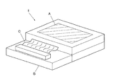
- FIG. 1 is a schematic view showing an example of a display device composed of organic EL elements. It is a schematic diagram of a display such as a mobile phone that displays image information by light emission of an organic EL element.
- the display 1 includes a display unit A having a plurality of pixels, a control unit B that performs image scanning of the display unit A based on image information, a wiring unit C that electrically connects the display unit A and the control unit B, and the like.
- the control unit B is electrically connected via the display unit A and the wiring unit C, and sends a scanning signal and an image data signal to each of a plurality of pixels based on image information from the outside. Then, the pixels for each scanning line sequentially emit light in accordance with the image data signal by the scanning signal, and image scanning is performed to display image information on the display unit A.
- FIG. 2 is a schematic diagram of a display device using an active matrix system, and is a schematic diagram of a display unit A.
- the display unit A includes a wiring unit C including a plurality of scanning lines 5 and data lines 6, a plurality of pixels 3 and the like on a substrate. The main members of the display unit A will be described below.
- FIG. 2 shows a case where the light emitted from the pixel 3 (the emitted light L) is extracted in the white arrow direction (downward).
- the scanning line 5 and the plurality of data lines 6 in the wiring portion are each made of a conductive material, and the scanning lines 5 and the data lines 6 are orthogonal to each other in a grid pattern and are connected to the pixels 3 at the orthogonal positions (details are illustrated Not)
- the pixel 3 receives an image data signal from the data line 6 and emits light according to the received image data.
- Full-color display is possible by appropriately arranging pixels in the red region, the green region, and the blue region on the same substrate.
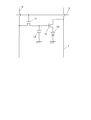
- FIG. 3 is a schematic diagram showing a pixel circuit.
- the pixel includes an organic EL element 10, a switching transistor 11, a driving transistor 12, a capacitor 13, and the like.
- a full color display can be performed by using red, green, and blue light emitting organic EL elements as the organic EL elements 10 in a plurality of pixels, and juxtaposing them on the same substrate.
- an image data signal is applied from the control unit B to the drain of the switching transistor 11 via the data line 6.
- the scanning signal is applied from the control unit B to the gate of the switching transistor 11 through the scanning line 5
- the driving of the switching transistor 11 is turned on. Then, the image data signal applied to the drain is transmitted to the capacitor 13 and the gate of the driving transistor 12.
- the capacitor 13 is charged according to the potential of the image data signal, and the drive transistor 12 is turned on.
- the drive transistor 12 has a drain connected to the power supply line 7 and a source connected to the electrode of the organic EL element 10, and the power supply line 7 connects to the organic EL element 10 according to the potential of the image data signal applied to the gate. Current is supplied.
- the driving of the switching transistor 11 is turned off. However, even if the driving of the switching transistor 11 is turned off, the capacitor 13 holds the potential of the charged image data signal, so that the driving of the driving transistor 12 is kept on. The light emission of the organic EL element 10 continues until the next scanning signal is applied.
- the driving transistor 12 is driven according to the potential of the next image data signal synchronized with the scanning signal, and the organic EL element 10 emits light.
- the organic EL element 10 emits light by the switching transistor 11 and the drive transistor 12 that are active elements for the organic EL element 10 of each of the plurality of pixels, and the light emission of the organic EL element 10 of each of the plurality of pixels 3. It is carried out.
- Such a light emitting method is called an active matrix method.
- the light emission of the organic EL element 10 may be light emission of a plurality of gradations by a multi-value image data signal having a plurality of gradation potentials, or by turning on / off a predetermined light emission amount by a binary image data signal. Good.
- the potential of the capacitor 13 may be held continuously until the next scanning signal is applied, or may be discharged immediately before the next scanning signal is applied.
- a passive matrix light emission drive in which the organic EL element emits light according to the data signal only when the scanning signal is scanned.
- FIG. 4 is a schematic view of a passive matrix display device.
- a plurality of scanning lines 5 and a plurality of image data lines 6 are provided in a lattice shape so as to face each other with the pixel 3 interposed therebetween.
- the scanning signal of the scanning line 5 is applied by sequential scanning, the pixels 3 connected to the applied scanning line 5 emit light according to the image data signal.
- the pixel 3 has no active element, and the manufacturing cost can be reduced.
- the organic EL element of the present invention By using the organic EL element of the present invention, a display device with improved luminous efficiency was obtained.
- the organic EL element of the present invention can also be used for a lighting device.
- the lighting device of the present invention includes the organic EL element of the present invention.
- the organic EL element of the present invention may be used as an organic EL element having a resonator structure. Examples of the purpose of use of the organic EL element having such a resonator structure include a light source of an optical storage medium, a light source of an electrophotographic copying machine, a light source of an optical communication processing machine, and a light source of an optical sensor. It is not limited. Moreover, you may use for the said use by making a laser oscillation.
- the organic EL element of the present invention may be used as a kind of lamp for illumination or exposure light source, a projection device for projecting an image, or a type for directly viewing a still image or a moving image. It may be used as a display device (display).
- the driving method when used as a display device for reproducing a moving image may be either a passive matrix method or an active matrix method. Alternatively, it is possible to produce a full-color display device by using two or more organic EL elements of the present invention having different emission colors.
- white light emission can be obtained by simultaneously emitting a plurality of light emission colors and mixing the colors.
- the light emission may include three light emission maximum wavelengths of three primary colors of red, green and blue, or two light emission utilizing a complementary color relationship such as blue and yellow, blue green and orange, etc. It may contain a maximum wavelength.
- the method for forming the organic EL device of the present invention may be simply arranged by providing a mask only when forming a light emitting layer, a hole transport layer, an electron transport layer, or the like, and separately coating with the mask. Since the other layers are common, patterning of a mask or the like is unnecessary, and for example, an electrode film can be formed on one surface by a vapor deposition method, a cast method, a spin coating method, an ink jet method, a printing method, or the like, and productivity is improved. According to this method, unlike a white organic EL device in which light emitting elements of a plurality of colors are arranged in parallel in an array, the elements themselves are luminescent white.
- the non-light-emitting surface of the organic EL element of the present invention is covered with a glass case, and a glass substrate having a thickness of 300 ⁇ m is used as a sealing substrate.
- An epoxy photo-curing adhesive (Lux Track LC0629B manufactured by Toagosei Co., Ltd.) is applied as a sealant around the periphery, and this is stacked on the cathode and brought into close contact with the transparent support substrate. Then, UV light is irradiated from the glass substrate side to be cured and sealed, and an illumination device as shown in FIGS. 5 and 6 can be formed.
- FIG. 5 and 6 An illumination device as shown in FIGS. 5 and 6 can be formed.
- FIG. 5 shows a schematic diagram of the lighting device, and the organic EL element of the present invention (organic EL element 101 in the lighting device) is covered with a glass cover 102 (note that the sealing operation with the glass cover is performed by lighting. This was performed in a glove box under a nitrogen atmosphere (in an atmosphere of high-purity nitrogen gas having a purity of 99.999% or more) without bringing the organic EL element 101 in the apparatus into contact with the air.
- 6 shows a cross-sectional view of the lighting device.
- reference numeral 105 denotes a cathode
- 106 denotes an organic functional layer
- 107 denotes a glass substrate with a transparent electrode.
- the glass cover 102 is filled with nitrogen gas 108 and a water catching agent 109 is provided.
- Example 1 (Production of organic EL element) ⁇ Preparation of organic EL element 1-1> An ITO (indium tin oxide) film having a thickness of 150 nm was formed as an anode on a glass substrate having a size of 50 mm ⁇ 50 mm and a thickness of 0.7 mm. After patterning, the transparent substrate with the ITO transparent electrode was ultrasonically cleaned with isopropyl alcohol. Subsequently, it dried with dry nitrogen gas and performed UV ozone cleaning for 5 minutes. Thereafter, this transparent substrate was fixed to a substrate holder of a commercially available vacuum deposition apparatus.
- ITO indium tin oxide
- Each of the vapor deposition crucibles in the vacuum vapor deposition apparatus was filled with the constituent material of each layer in an amount optimal for device fabrication.
- the evaporation crucible used was made of a resistance heating material made of molybdenum or tungsten. After reducing the pressure to 1 ⁇ 10 ⁇ 4 Pa, the evaporation crucible containing HAT-CN (1,4,5,8,9,12-hexaazatriphenylenehexacarbonitrile) was energized and heated. And it vapor-deposited on the ITO transparent electrode with the vapor deposition rate of 0.1 nm / sec, and formed the 10-nm-thick hole injection layer.
- ⁇ -NPD 4,4′-bis [N- (1-naphthyl) -N-phenylamino] biphenyl
- the hole transport layer was formed.
- CBP 4,4′-Bis (carbazol-9-yl) biphenyl) as the host compound and Ir (ppy) 3 as the luminescent dopant were deposited at a deposition rate of 0.1 nm / min so as to be 90% and 10% by volume, respectively.
- Co-evaporation was performed in seconds to form a light emitting layer having a layer thickness of 30 nm.
- the deposition rate was 0.1 nm / second so that the comparative compound 1 (electron transport layer (1)) and LiQ (8-hydroxyquinolinato lithium) (electron transport layer (2)) were 50% and 50% by volume, respectively.
- the comparative compound 1 (electron transport layer (1)) and LiQ (8-hydroxyquinolinato lithium) (electron transport layer (2)) were 50% and 50% by volume, respectively.
- 100 nm of aluminum was vapor-deposited to form a cathode.
- the non-light-emitting surface side of the above element was covered with a can-shaped glass case in an atmosphere of high purity nitrogen gas having a purity of 99.999% or more, and an electrode lead-out wiring was installed to prepare an organic EL element 1-1.
- organic EL elements 1-2 to 1-30 were prepared in the same manner as the organic EL element 1-1 except that the compounds contained in the electron transport layers (1) and (2) and the electron injection layer were changed as shown in Table 1. 30 was produced. In Table 1, “-” indicates that no component is contained.
- Example 2 (Production of organic EL element) ⁇ Preparation of organic EL element 2-1> A transparent substrate with an ITO (Indium Tin Oxide) film having a thickness of 150 nm formed on a glass substrate of 50 mm ⁇ 50 mm and a thickness of 0.7 mm, patterned, and this ITO transparent electrode was attached After ultrasonic cleaning with isopropyl alcohol, drying with dry nitrogen gas and UV ozone cleaning for 5 minutes, this transparent substrate was fixed to a substrate holder of a commercially available vacuum deposition apparatus.
- ITO Indium Tin Oxide
- Each of the vapor deposition crucibles in the vacuum vapor deposition apparatus was filled with the constituent material of each layer in an amount optimal for device fabrication.
- the evaporation crucible used was made of a resistance heating material made of molybdenum or tungsten. After reducing the vacuum to 1 ⁇ 10 ⁇ 4 Pa, energize and heat the evaporation crucible containing HAT-CN (1,4,5,8,9,12-hexaazatriphenylenehexacarbonitrile) to evaporate Vapor deposition was performed on the ITO transparent electrode at a rate of 0.1 nm / second to form a hole injection layer having a layer thickness of 10 nm.
- ⁇ -NPD 4,4′-bis [N- (1-naphthyl) -N-phenylamino] biphenyl
- the hole transport layer was formed.
- CBP as a host compound and Ir (ppy) 3 as a light emitting dopant were co-deposited at a deposition rate of 0.1 nm / second so as to be 90% and 10% by volume, respectively, to form a light emitting layer having a layer thickness of 30 nm.
- Comparative Compound 2 and KF were co-deposited at a deposition rate of 0.1 nm / second so as to be 85% and 15% by volume, respectively, to form an electron transport layer having a layer thickness of 30 nm.
- silver was deposited at a deposition rate of 0.1 nm / second to form a cathode having a thickness of 15 nm.
- the non-light-emitting surface side of the above element was covered with a can-shaped glass case in an atmosphere of high purity nitrogen gas having a purity of 99.999% or more, and an electrode lead-out wiring was installed to produce an organic EL element 2-1.
- organic EL elements 2-2 to 2-21 were the same as the organic EL element 2-1, except that the compound of the electron transport layer, the ratio of silver and magnesium of the cathode, and the film thickness of the cathode were changed as shown in Table 2. 21 was produced.
- the electron transport layer contains 15% KF, but in Table 2, the notation of KF is omitted.
- Example 3 (Production of organic EL element) ⁇ Preparation of organic EL element 3-1> An ITO (indium tin oxide) film having a thickness of 150 nm was formed as an anode on a glass substrate having a size of 50 mm ⁇ 50 mm and a thickness of 0.7 mm. After patterning, the transparent substrate with the ITO transparent electrode was ultrasonically cleaned with isopropyl alcohol. Subsequently, it dried with dry nitrogen gas and performed UV ozone cleaning for 5 minutes. Thereafter, this transparent substrate was fixed to a substrate holder of a commercially available vacuum deposition apparatus.
- ITO indium tin oxide
- Each of the vapor deposition crucibles in the vacuum vapor deposition apparatus was filled with the constituent material of each layer in an amount optimal for device fabrication.
- the evaporation crucible used was made of a resistance heating material made of molybdenum or tungsten. After reducing the pressure to 1 ⁇ 10 ⁇ 4 Pa, the evaporation crucible containing HAT-CN (1,4,5,8,9,12-hexaazatriphenylenehexacarbonitrile) was energized and heated. And it vapor-deposited on the ITO transparent electrode with the vapor deposition rate of 0.1 nm / sec, and formed the 10-nm-thick hole injection layer.
- ⁇ -NPD 4,4′-bis [N- (1-naphthyl) -N-phenylamino] biphenyl
- the hole transport layer was formed.
- CBP as a host compound and Ir (ppy) 3 as a light emitting dopant were co-deposited at a deposition rate of 0.1 nm / second so as to be 90% and 10% by volume, respectively, to form a light emitting layer having a layer thickness of 30 nm.
- Alq 3 was deposited as an electron transport layer at a deposition rate of 0.1 nm / second to form an electron transport layer having a layer thickness of 30 nm.
- Comparative Compound 3 and LiQ were co-deposited at a deposition rate of 0.1 nm / second so as to be 50% and 50% by volume, respectively, to form an electron injection layer having a layer thickness of 2 nm.
- silver and magnesium were co-deposited at a deposition rate of 0.1 nm / second and 0.01 nm / second, respectively, to form a cathode having a thickness of 8 nm.
- the non-light-emitting surface side of the above element was covered with a can-shaped glass case in an atmosphere of high purity nitrogen gas with a purity of 99.999% or more, and an electrode lead-out wiring was installed to prepare an organic EL element 3-1.
- the organic EL devices 3-2 to 3-3 were the same as the organic EL device 3-1, except that the compound of the electron injection layer, the ratio of silver and magnesium of the cathode, and the thickness of the cathode were changed as shown in Table 3. 17 was produced.
- 50% of LiQ is contained in the electron injection layer, but the LiQ notation is omitted in Table 3.
- the organic EL device of the present invention has a lower relative driving voltage than the organic EL device of the comparative example and a smaller change in the relative driving voltage under high temperature storage, so that it has excellent stability during high temperature storage and durability. I found it excellent.
Abstract
La présente invention aborde le problème consistant à fournir un élément d'électroluminescence organique dans lequel une stabilité pendant le stockage à haute température et la tension d'attaque sont améliorées ; un matériau pour électroluminescence organique utilisé dans l'élément d'électroluminescence organique, un dispositif d'affichage et un dispositif d'éclairage. Cet élément d'électroluminescence organique a une électrode positive, une pluralité de couches fonctionnelles organiques comprenant une couche électroluminescente, et une électrode négative dans l'ordre indiqué, l'élément d'électroluminescence organique ayant, entre la couche électroluminescente et l'électrode négative, une couche fonctionnelle organique contenant un composé qui a une structure représentée par la formule générale (1).
Applications Claiming Priority (2)
| Application Number | Priority Date | Filing Date | Title |
|---|---|---|---|
| JP2018-048544 | 2018-03-15 | ||
| JP2018048544 | 2018-03-15 |
Publications (1)
| Publication Number | Publication Date |
|---|---|
| WO2019176384A1 true WO2019176384A1 (fr) | 2019-09-19 |
Family
ID=67908276
Family Applications (1)
| Application Number | Title | Priority Date | Filing Date |
|---|---|---|---|
| PCT/JP2019/004099 WO2019176384A1 (fr) | 2018-03-15 | 2019-02-05 | Élément d'électroluminescence organique, matériau pour électroluminescence organique, dispositif d'affichage et dispositif d'éclairage |
Country Status (1)
| Country | Link |
|---|---|
| WO (1) | WO2019176384A1 (fr) |
Citations (9)
| Publication number | Priority date | Publication date | Assignee | Title |
|---|---|---|---|---|
| CN103570629A (zh) * | 2012-07-27 | 2014-02-12 | 昆山维信诺显示技术有限公司 | 一种含有嘧啶或吡嗪或三嗪基团的苯并蒽衍生物及应用 |
| CN103665014A (zh) * | 2012-08-30 | 2014-03-26 | 昆山维信诺显示技术有限公司 | 一种6-三甲苯基-6H-6-硼杂苯并[cd]芘衍生物及其应用 |
| JP2015504422A (ja) * | 2011-11-10 | 2015-02-12 | ビーエーエスエフ ソシエタス・ヨーロピアBasf Se | エレクトロニクス用途のための4H−イミダゾ[1,2−a]イミダゾール |
| KR20150037318A (ko) * | 2013-09-30 | 2015-04-08 | 주식회사 엘지화학 | 헤테로환 화합물 및 이를 포함하는 유기 발광 소자 |
| JP2015524797A (ja) * | 2012-07-13 | 2015-08-27 | エルジー・ケム・リミテッド | ヘテロ環化合物およびこれを用いた有機電子素子 |
| KR20160041019A (ko) * | 2014-10-06 | 2016-04-15 | 희성소재 (주) | 헤테로고리 화합물 및 이를 이용한 유기 발광 소자 |
| JP2016538238A (ja) * | 2013-09-24 | 2016-12-08 | エルジー・ケム・リミテッド | ヘテロ環化合物およびこれを含む有機発光素子 |
| KR20180044832A (ko) * | 2016-10-24 | 2018-05-03 | 주식회사 엘지화학 | 유기 발광 소자 |
| KR20180115558A (ko) * | 2017-04-13 | 2018-10-23 | 주식회사 엘지화학 | 신규한 헤테로 고리 화합물 및 이를 이용한 유기발광 소자 |
-
2019
- 2019-02-05 WO PCT/JP2019/004099 patent/WO2019176384A1/fr active Application Filing
Patent Citations (9)
| Publication number | Priority date | Publication date | Assignee | Title |
|---|---|---|---|---|
| JP2015504422A (ja) * | 2011-11-10 | 2015-02-12 | ビーエーエスエフ ソシエタス・ヨーロピアBasf Se | エレクトロニクス用途のための4H−イミダゾ[1,2−a]イミダゾール |
| JP2015524797A (ja) * | 2012-07-13 | 2015-08-27 | エルジー・ケム・リミテッド | ヘテロ環化合物およびこれを用いた有機電子素子 |
| CN103570629A (zh) * | 2012-07-27 | 2014-02-12 | 昆山维信诺显示技术有限公司 | 一种含有嘧啶或吡嗪或三嗪基团的苯并蒽衍生物及应用 |
| CN103665014A (zh) * | 2012-08-30 | 2014-03-26 | 昆山维信诺显示技术有限公司 | 一种6-三甲苯基-6H-6-硼杂苯并[cd]芘衍生物及其应用 |
| JP2016538238A (ja) * | 2013-09-24 | 2016-12-08 | エルジー・ケム・リミテッド | ヘテロ環化合物およびこれを含む有機発光素子 |
| KR20150037318A (ko) * | 2013-09-30 | 2015-04-08 | 주식회사 엘지화학 | 헤테로환 화합물 및 이를 포함하는 유기 발광 소자 |
| KR20160041019A (ko) * | 2014-10-06 | 2016-04-15 | 희성소재 (주) | 헤테로고리 화합물 및 이를 이용한 유기 발광 소자 |
| KR20180044832A (ko) * | 2016-10-24 | 2018-05-03 | 주식회사 엘지화학 | 유기 발광 소자 |
| KR20180115558A (ko) * | 2017-04-13 | 2018-10-23 | 주식회사 엘지화학 | 신규한 헤테로 고리 화합물 및 이를 이용한 유기발광 소자 |
Similar Documents
| Publication | Publication Date | Title |
|---|---|---|
| JP5810529B2 (ja) | 有機エレクトロルミネッセンス素子、表示装置及び照明装置 | |
| JP5747736B2 (ja) | 有機エレクトロルミネッセンス素子、表示装置及び照明装置 | |
| JP5493309B2 (ja) | 有機エレクトロルミネッセンス素子材料、有機エレクトロルミネッセンス素子、表示装置及び照明装置 | |
| WO2013168688A1 (fr) | Élément à électroluminescence organique, dispositif d'éclairage et dispositif d'affichage | |
| CN109863614B (zh) | 有机电致发光元件及有机电致发光用材料 | |
| JP6146415B2 (ja) | 有機エレクトロルミネッセンス素子、照明装置及び表示装置 | |
| JP6011542B2 (ja) | 有機エレクトロルミネッセンス素子、表示装置及び照明装置 | |
| JP2015213119A (ja) | 有機エレクトロルミネッセンス素子用材料、有機エレクトロルミネッセンス素子、照明装置及び表示装置 | |
| WO2016175068A1 (fr) | Matériau pour éléments électroluminescents organiques, élément électroluminescent organique, dispositif d'affichage et dispositif d'éclairage | |
| WO2016056562A1 (fr) | Complexe d'iridium, matériau électroluminescent organique, élément électroluminescent organique, dispositif d'affichage et dispositif d'éclairage | |
| WO2015046452A1 (fr) | Complexe d'iridium, procédé de production de complexe d'iridium, élément électroluminescent organique, dispositif d'affichage et dispositif d'éclairage | |
| JP4941291B2 (ja) | 有機エレクトロルミネッセンス素子 | |
| JP6020466B2 (ja) | 有機エレクトロルミネッセンス素子、表示装置及び照明装置 | |
| JP7173145B2 (ja) | 薄膜、電子デバイス、有機エレクトロルミネッセンス素子、有機エレクトロルミネッセンス用材料、表示装置、及び、照明装置 | |
| WO2019107424A1 (fr) | Élément électroluminescent organique, matériau électroluminescent organique, dispositif d'affichage, et dispositif d'éclairage | |
| WO2019176384A1 (fr) | Élément d'électroluminescence organique, matériau pour électroluminescence organique, dispositif d'affichage et dispositif d'éclairage | |
| JP7029404B2 (ja) | 有機エレクトロルミネッセンス素子及び有機エレクトロルミネッセンス用材料 | |
| WO2013161468A1 (fr) | Élément électroluminescent organique | |
| WO2013137162A1 (fr) | Élément électroluminescent organique, dispositif d'éclairage et dispositif d'affichage | |
| JP5930005B2 (ja) | 有機エレクトロルミネッセンス素子材料、有機エレクトロルミネッセンス素子及びその製造方法、表示装置並びに照明装置 | |
| JP5708759B2 (ja) | 有機エレクトロルミネッセンス素子材料、有機エレクトロルミネッセンス素子、表示装置及び照明装置 | |
| JP5673746B2 (ja) | 有機エレクトロルミネッセンス素子 | |
| JP5359441B2 (ja) | 有機エレクトロルミネッセンス素子材料、有機エレクトロルミネッセンス素子、表示装置及び照明装置 |
Legal Events
| Date | Code | Title | Description |
|---|---|---|---|
| 121 | Ep: the epo has been informed by wipo that ep was designated in this application |
Ref document number: 19767663 Country of ref document: EP Kind code of ref document: A1 |
|
| NENP | Non-entry into the national phase |
Ref country code: DE |
|
| 122 | Ep: pct application non-entry in european phase |
Ref document number: 19767663 Country of ref document: EP Kind code of ref document: A1 |
|
| NENP | Non-entry into the national phase |
Ref country code: JP |