WO2019171204A1 - 表示装置および電子機器 - Google Patents
表示装置および電子機器 Download PDFInfo
- Publication number
- WO2019171204A1 WO2019171204A1 PCT/IB2019/051513 IB2019051513W WO2019171204A1 WO 2019171204 A1 WO2019171204 A1 WO 2019171204A1 IB 2019051513 W IB2019051513 W IB 2019051513W WO 2019171204 A1 WO2019171204 A1 WO 2019171204A1
- Authority
- WO
- WIPO (PCT)
- Prior art keywords
- transistor
- electrode
- electrically connected
- wiring
- node
- Prior art date
Links
- 230000008878 coupling Effects 0.000 claims abstract description 12
- 238000010168 coupling process Methods 0.000 claims abstract description 12
- 238000005859 coupling reaction Methods 0.000 claims abstract description 12
- 239000003990 capacitor Substances 0.000 claims description 86
- 230000006870 function Effects 0.000 claims description 72
- 239000004973 liquid crystal related substance Substances 0.000 claims description 65
- 230000015572 biosynthetic process Effects 0.000 claims description 13
- 229910044991 metal oxide Inorganic materials 0.000 claims description 11
- 150000004706 metal oxides Chemical class 0.000 claims description 11
- 229910052733 gallium Inorganic materials 0.000 claims description 9
- 229910052738 indium Inorganic materials 0.000 claims description 9
- 229910052719 titanium Inorganic materials 0.000 claims description 8
- 229910052782 aluminium Inorganic materials 0.000 claims description 7
- 229910052725 zinc Inorganic materials 0.000 claims description 6
- 229910052684 Cerium Inorganic materials 0.000 claims description 5
- 229910052779 Neodymium Inorganic materials 0.000 claims description 5
- 229910052735 hafnium Inorganic materials 0.000 claims description 5
- 229910052746 lanthanum Inorganic materials 0.000 claims description 5
- 229910052727 yttrium Inorganic materials 0.000 claims description 5
- 229910052726 zirconium Inorganic materials 0.000 claims description 5
- 229910052732 germanium Inorganic materials 0.000 claims description 4
- 229910052718 tin Inorganic materials 0.000 claims description 3
- 239000010410 layer Substances 0.000 description 243
- 239000004065 semiconductor Substances 0.000 description 133
- 238000000034 method Methods 0.000 description 49
- 239000000758 substrate Substances 0.000 description 48
- 239000000463 material Substances 0.000 description 39
- 239000011701 zinc Substances 0.000 description 33
- 239000010408 film Substances 0.000 description 30
- 229920005989 resin Polymers 0.000 description 23
- 239000011347 resin Substances 0.000 description 23
- 238000003860 storage Methods 0.000 description 20
- 239000013078 crystal Substances 0.000 description 16
- 230000001965 increasing effect Effects 0.000 description 16
- 229910052760 oxygen Inorganic materials 0.000 description 16
- 229910052751 metal Inorganic materials 0.000 description 15
- 238000000149 argon plasma sintering Methods 0.000 description 14
- QVGXLLKOCUKJST-UHFFFAOYSA-N atomic oxygen Chemical compound [O] QVGXLLKOCUKJST-UHFFFAOYSA-N 0.000 description 14
- 239000002131 composite material Substances 0.000 description 14
- 239000001301 oxygen Substances 0.000 description 14
- 125000004429 atom Chemical group 0.000 description 12
- 239000012535 impurity Substances 0.000 description 12
- 239000002184 metal Substances 0.000 description 12
- 150000001875 compounds Chemical class 0.000 description 10
- IJGRMHOSHXDMSA-UHFFFAOYSA-N Atomic nitrogen Chemical compound N#N IJGRMHOSHXDMSA-UHFFFAOYSA-N 0.000 description 9
- 238000009792 diffusion process Methods 0.000 description 9
- 239000001257 hydrogen Substances 0.000 description 9
- 229910052739 hydrogen Inorganic materials 0.000 description 9
- UFHFLCQGNIYNRP-UHFFFAOYSA-N Hydrogen Chemical compound [H][H] UFHFLCQGNIYNRP-UHFFFAOYSA-N 0.000 description 8
- XLOMVQKBTHCTTD-UHFFFAOYSA-N Zinc monoxide Chemical compound [Zn]=O XLOMVQKBTHCTTD-UHFFFAOYSA-N 0.000 description 8
- 238000004519 manufacturing process Methods 0.000 description 8
- 238000004088 simulation Methods 0.000 description 8
- 239000010936 titanium Substances 0.000 description 8
- PXHVJJICTQNCMI-UHFFFAOYSA-N Nickel Chemical compound [Ni] PXHVJJICTQNCMI-UHFFFAOYSA-N 0.000 description 7
- 239000000969 carrier Substances 0.000 description 7
- 230000007547 defect Effects 0.000 description 7
- 238000001514 detection method Methods 0.000 description 7
- 230000005684 electric field Effects 0.000 description 7
- 230000003287 optical effect Effects 0.000 description 7
- 239000000565 sealant Substances 0.000 description 7
- XUIMIQQOPSSXEZ-UHFFFAOYSA-N Silicon Chemical compound [Si] XUIMIQQOPSSXEZ-UHFFFAOYSA-N 0.000 description 6
- RTAQQCXQSZGOHL-UHFFFAOYSA-N Titanium Chemical compound [Ti] RTAQQCXQSZGOHL-UHFFFAOYSA-N 0.000 description 6
- 239000000203 mixture Substances 0.000 description 6
- 229910052710 silicon Inorganic materials 0.000 description 6
- 239000010703 silicon Substances 0.000 description 6
- GYHNNYVSQQEPJS-UHFFFAOYSA-N Gallium Chemical compound [Ga] GYHNNYVSQQEPJS-UHFFFAOYSA-N 0.000 description 5
- XAGFODPZIPBFFR-UHFFFAOYSA-N aluminium Chemical compound [Al] XAGFODPZIPBFFR-UHFFFAOYSA-N 0.000 description 5
- 239000003086 colorant Substances 0.000 description 5
- 230000005669 field effect Effects 0.000 description 5
- APFVFJFRJDLVQX-UHFFFAOYSA-N indium atom Chemical compound [In] APFVFJFRJDLVQX-UHFFFAOYSA-N 0.000 description 5
- 230000007246 mechanism Effects 0.000 description 5
- 125000006850 spacer group Chemical group 0.000 description 5
- XKRFYHLGVUSROY-UHFFFAOYSA-N Argon Chemical compound [Ar] XKRFYHLGVUSROY-UHFFFAOYSA-N 0.000 description 4
- XEEYBQQBJWHFJM-UHFFFAOYSA-N Iron Chemical compound [Fe] XEEYBQQBJWHFJM-UHFFFAOYSA-N 0.000 description 4
- 239000010949 copper Substances 0.000 description 4
- 238000010894 electron beam technology Methods 0.000 description 4
- 238000000295 emission spectrum Methods 0.000 description 4
- 238000002149 energy-dispersive X-ray emission spectroscopy Methods 0.000 description 4
- 230000002349 favourable effect Effects 0.000 description 4
- 239000000945 filler Substances 0.000 description 4
- 239000011521 glass Substances 0.000 description 4
- VBJZVLUMGGDVMO-UHFFFAOYSA-N hafnium atom Chemical compound [Hf] VBJZVLUMGGDVMO-UHFFFAOYSA-N 0.000 description 4
- 229910003437 indium oxide Inorganic materials 0.000 description 4
- PJXISJQVUVHSOJ-UHFFFAOYSA-N indium(iii) oxide Chemical compound [O-2].[O-2].[O-2].[In+3].[In+3] PJXISJQVUVHSOJ-UHFFFAOYSA-N 0.000 description 4
- 239000002105 nanoparticle Substances 0.000 description 4
- 229910052757 nitrogen Inorganic materials 0.000 description 4
- 238000005192 partition Methods 0.000 description 4
- 230000002093 peripheral effect Effects 0.000 description 4
- 239000011241 protective layer Substances 0.000 description 4
- 238000001004 secondary ion mass spectrometry Methods 0.000 description 4
- 239000000126 substance Substances 0.000 description 4
- 239000010409 thin film Substances 0.000 description 4
- WFKWXMTUELFFGS-UHFFFAOYSA-N tungsten Chemical compound [W] WFKWXMTUELFFGS-UHFFFAOYSA-N 0.000 description 4
- 229910052721 tungsten Inorganic materials 0.000 description 4
- 239000010937 tungsten Substances 0.000 description 4
- 239000011787 zinc oxide Substances 0.000 description 4
- OKTJSMMVPCPJKN-UHFFFAOYSA-N Carbon Chemical compound [C] OKTJSMMVPCPJKN-UHFFFAOYSA-N 0.000 description 3
- RYGMFSIKBFXOCR-UHFFFAOYSA-N Copper Chemical compound [Cu] RYGMFSIKBFXOCR-UHFFFAOYSA-N 0.000 description 3
- MYMOFIZGZYHOMD-UHFFFAOYSA-N Dioxygen Chemical compound O=O MYMOFIZGZYHOMD-UHFFFAOYSA-N 0.000 description 3
- ZOKXTWBITQBERF-UHFFFAOYSA-N Molybdenum Chemical compound [Mo] ZOKXTWBITQBERF-UHFFFAOYSA-N 0.000 description 3
- 239000004983 Polymer Dispersed Liquid Crystal Substances 0.000 description 3
- QCWXUUIWCKQGHC-UHFFFAOYSA-N Zirconium Chemical compound [Zr] QCWXUUIWCKQGHC-UHFFFAOYSA-N 0.000 description 3
- 229910052799 carbon Inorganic materials 0.000 description 3
- ZMIGMASIKSOYAM-UHFFFAOYSA-N cerium Chemical compound [Ce][Ce][Ce][Ce][Ce][Ce][Ce][Ce][Ce][Ce][Ce][Ce][Ce][Ce][Ce][Ce][Ce][Ce][Ce][Ce][Ce][Ce][Ce][Ce][Ce][Ce][Ce][Ce][Ce][Ce][Ce][Ce][Ce][Ce][Ce][Ce][Ce][Ce] ZMIGMASIKSOYAM-UHFFFAOYSA-N 0.000 description 3
- 229920001940 conductive polymer Polymers 0.000 description 3
- 239000004020 conductor Substances 0.000 description 3
- 229910052802 copper Inorganic materials 0.000 description 3
- 229910001882 dioxygen Inorganic materials 0.000 description 3
- GNPVGFCGXDBREM-UHFFFAOYSA-N germanium atom Chemical compound [Ge] GNPVGFCGXDBREM-UHFFFAOYSA-N 0.000 description 3
- 229910010272 inorganic material Inorganic materials 0.000 description 3
- FZLIPJUXYLNCLC-UHFFFAOYSA-N lanthanum atom Chemical compound [La] FZLIPJUXYLNCLC-UHFFFAOYSA-N 0.000 description 3
- 229910052750 molybdenum Inorganic materials 0.000 description 3
- 239000011733 molybdenum Substances 0.000 description 3
- QEFYFXOXNSNQGX-UHFFFAOYSA-N neodymium atom Chemical compound [Nd] QEFYFXOXNSNQGX-UHFFFAOYSA-N 0.000 description 3
- 229910052759 nickel Inorganic materials 0.000 description 3
- BASFCYQUMIYNBI-UHFFFAOYSA-N platinum Chemical compound [Pt] BASFCYQUMIYNBI-UHFFFAOYSA-N 0.000 description 3
- 229920000642 polymer Polymers 0.000 description 3
- 230000001681 protective effect Effects 0.000 description 3
- 238000005477 sputtering target Methods 0.000 description 3
- 229910052715 tantalum Inorganic materials 0.000 description 3
- GUVRBAGPIYLISA-UHFFFAOYSA-N tantalum atom Chemical compound [Ta] GUVRBAGPIYLISA-UHFFFAOYSA-N 0.000 description 3
- VWQVUPCCIRVNHF-UHFFFAOYSA-N yttrium atom Chemical compound [Y] VWQVUPCCIRVNHF-UHFFFAOYSA-N 0.000 description 3
- YVTHLONGBIQYBO-UHFFFAOYSA-N zinc indium(3+) oxygen(2-) Chemical compound [O--].[Zn++].[In+3] YVTHLONGBIQYBO-UHFFFAOYSA-N 0.000 description 3
- PAYRUJLWNCNPSJ-UHFFFAOYSA-N Aniline Chemical compound NC1=CC=CC=C1 PAYRUJLWNCNPSJ-UHFFFAOYSA-N 0.000 description 2
- ZOXJGFHDIHLPTG-UHFFFAOYSA-N Boron Chemical compound [B] ZOXJGFHDIHLPTG-UHFFFAOYSA-N 0.000 description 2
- CURLTUGMZLYLDI-UHFFFAOYSA-N Carbon dioxide Chemical compound O=C=O CURLTUGMZLYLDI-UHFFFAOYSA-N 0.000 description 2
- FYYHWMGAXLPEAU-UHFFFAOYSA-N Magnesium Chemical compound [Mg] FYYHWMGAXLPEAU-UHFFFAOYSA-N 0.000 description 2
- KAESVJOAVNADME-UHFFFAOYSA-N Pyrrole Chemical compound C=1C=CNC=1 KAESVJOAVNADME-UHFFFAOYSA-N 0.000 description 2
- 229910052581 Si3N4 Inorganic materials 0.000 description 2
- YTPLMLYBLZKORZ-UHFFFAOYSA-N Thiophene Chemical compound C=1C=CSC=1 YTPLMLYBLZKORZ-UHFFFAOYSA-N 0.000 description 2
- GWEVSGVZZGPLCZ-UHFFFAOYSA-N Titan oxide Chemical compound O=[Ti]=O GWEVSGVZZGPLCZ-UHFFFAOYSA-N 0.000 description 2
- 238000002441 X-ray diffraction Methods 0.000 description 2
- HCHKCACWOHOZIP-UHFFFAOYSA-N Zinc Chemical compound [Zn] HCHKCACWOHOZIP-UHFFFAOYSA-N 0.000 description 2
- 229910052783 alkali metal Inorganic materials 0.000 description 2
- 150000001340 alkali metals Chemical class 0.000 description 2
- 229910052784 alkaline earth metal Inorganic materials 0.000 description 2
- 150000001342 alkaline earth metals Chemical class 0.000 description 2
- 229910052786 argon Inorganic materials 0.000 description 2
- 229910052790 beryllium Inorganic materials 0.000 description 2
- ATBAMAFKBVZNFJ-UHFFFAOYSA-N beryllium atom Chemical compound [Be] ATBAMAFKBVZNFJ-UHFFFAOYSA-N 0.000 description 2
- 229910052796 boron Inorganic materials 0.000 description 2
- DQXBYHZEEUGOBF-UHFFFAOYSA-N but-3-enoic acid;ethene Chemical compound C=C.OC(=O)CC=C DQXBYHZEEUGOBF-UHFFFAOYSA-N 0.000 description 2
- 230000008859 change Effects 0.000 description 2
- 239000011651 chromium Substances 0.000 description 2
- 238000000576 coating method Methods 0.000 description 2
- 238000004891 communication Methods 0.000 description 2
- PMHQVHHXPFUNSP-UHFFFAOYSA-M copper(1+);methylsulfanylmethane;bromide Chemical compound Br[Cu].CSC PMHQVHHXPFUNSP-UHFFFAOYSA-M 0.000 description 2
- 238000000151 deposition Methods 0.000 description 2
- 230000008021 deposition Effects 0.000 description 2
- 239000002274 desiccant Substances 0.000 description 2
- 230000006866 deterioration Effects 0.000 description 2
- 238000010586 diagram Methods 0.000 description 2
- 230000000694 effects Effects 0.000 description 2
- 230000005611 electricity Effects 0.000 description 2
- 239000005038 ethylene vinyl acetate Substances 0.000 description 2
- 230000005281 excited state Effects 0.000 description 2
- 239000000284 extract Substances 0.000 description 2
- 239000007789 gas Substances 0.000 description 2
- 238000003384 imaging method Methods 0.000 description 2
- AMGQUBHHOARCQH-UHFFFAOYSA-N indium;oxotin Chemical compound [In].[Sn]=O AMGQUBHHOARCQH-UHFFFAOYSA-N 0.000 description 2
- 239000011261 inert gas Substances 0.000 description 2
- 150000002484 inorganic compounds Chemical class 0.000 description 2
- 239000011810 insulating material Substances 0.000 description 2
- 229910052742 iron Inorganic materials 0.000 description 2
- 229910052749 magnesium Inorganic materials 0.000 description 2
- 239000011777 magnesium Substances 0.000 description 2
- 238000005259 measurement Methods 0.000 description 2
- 238000002156 mixing Methods 0.000 description 2
- 239000000178 monomer Substances 0.000 description 2
- 239000010955 niobium Substances 0.000 description 2
- QGLKJKCYBOYXKC-UHFFFAOYSA-N nonaoxidotritungsten Chemical compound O=[W]1(=O)O[W](=O)(=O)O[W](=O)(=O)O1 QGLKJKCYBOYXKC-UHFFFAOYSA-N 0.000 description 2
- 150000002894 organic compounds Chemical class 0.000 description 2
- 230000003071 parasitic effect Effects 0.000 description 2
- 239000002245 particle Substances 0.000 description 2
- 229920001200 poly(ethylene-vinyl acetate) Polymers 0.000 description 2
- 229920002037 poly(vinyl butyral) polymer Polymers 0.000 description 2
- 229920000915 polyvinyl chloride Polymers 0.000 description 2
- 239000004800 polyvinyl chloride Substances 0.000 description 2
- 230000008569 process Effects 0.000 description 2
- 239000002096 quantum dot Substances 0.000 description 2
- 238000011160 research Methods 0.000 description 2
- 239000003566 sealing material Substances 0.000 description 2
- HQVNEWCFYHHQES-UHFFFAOYSA-N silicon nitride Chemical compound N12[Si]34N5[Si]62N3[Si]51N64 HQVNEWCFYHHQES-UHFFFAOYSA-N 0.000 description 2
- 239000002356 single layer Substances 0.000 description 2
- 238000004544 sputter deposition Methods 0.000 description 2
- 230000003068 static effect Effects 0.000 description 2
- 229920001187 thermosetting polymer Polymers 0.000 description 2
- OGIDPMRJRNCKJF-UHFFFAOYSA-N titanium oxide Inorganic materials [Ti]=O OGIDPMRJRNCKJF-UHFFFAOYSA-N 0.000 description 2
- 238000002834 transmittance Methods 0.000 description 2
- 229910001930 tungsten oxide Inorganic materials 0.000 description 2
- 229910052720 vanadium Inorganic materials 0.000 description 2
- GPPXJZIENCGNKB-UHFFFAOYSA-N vanadium Chemical compound [V]#[V] GPPXJZIENCGNKB-UHFFFAOYSA-N 0.000 description 2
- 238000007740 vapor deposition Methods 0.000 description 2
- NIXOWILDQLNWCW-UHFFFAOYSA-M Acrylate Chemical compound [O-]C(=O)C=C NIXOWILDQLNWCW-UHFFFAOYSA-M 0.000 description 1
- 239000004925 Acrylic resin Substances 0.000 description 1
- 229920000178 Acrylic resin Polymers 0.000 description 1
- VYZAMTAEIAYCRO-UHFFFAOYSA-N Chromium Chemical compound [Cr] VYZAMTAEIAYCRO-UHFFFAOYSA-N 0.000 description 1
- 206010052128 Glare Diseases 0.000 description 1
- 206010021143 Hypoxia Diseases 0.000 description 1
- CERQOIWHTDAKMF-UHFFFAOYSA-M Methacrylate Chemical compound CC(=C)C([O-])=O CERQOIWHTDAKMF-UHFFFAOYSA-M 0.000 description 1
- 239000004988 Nematic liquid crystal Substances 0.000 description 1
- 239000004642 Polyimide Substances 0.000 description 1
- VYPSYNLAJGMNEJ-UHFFFAOYSA-N Silicium dioxide Chemical compound O=[Si]=O VYPSYNLAJGMNEJ-UHFFFAOYSA-N 0.000 description 1
- BQCADISMDOOEFD-UHFFFAOYSA-N Silver Chemical compound [Ag] BQCADISMDOOEFD-UHFFFAOYSA-N 0.000 description 1
- ATJFFYVFTNAWJD-UHFFFAOYSA-N Tin Chemical compound [Sn] ATJFFYVFTNAWJD-UHFFFAOYSA-N 0.000 description 1
- 239000000654 additive Substances 0.000 description 1
- 230000000996 additive effect Effects 0.000 description 1
- 229910045601 alloy Inorganic materials 0.000 description 1
- 239000000956 alloy Substances 0.000 description 1
- 229910021417 amorphous silicon Inorganic materials 0.000 description 1
- 230000008901 benefit Effects 0.000 description 1
- 239000011230 binding agent Substances 0.000 description 1
- 230000000903 blocking effect Effects 0.000 description 1
- 239000006229 carbon black Substances 0.000 description 1
- 229910002092 carbon dioxide Inorganic materials 0.000 description 1
- 239000001569 carbon dioxide Substances 0.000 description 1
- 229910052800 carbon group element Inorganic materials 0.000 description 1
- 230000015556 catabolic process Effects 0.000 description 1
- 238000006243 chemical reaction Methods 0.000 description 1
- 229910052804 chromium Inorganic materials 0.000 description 1
- 239000011248 coating agent Substances 0.000 description 1
- 229910017052 cobalt Inorganic materials 0.000 description 1
- 239000010941 cobalt Substances 0.000 description 1
- GUTLYIVDDKVIGB-UHFFFAOYSA-N cobalt atom Chemical compound [Co] GUTLYIVDDKVIGB-UHFFFAOYSA-N 0.000 description 1
- 238000004040 coloring Methods 0.000 description 1
- 239000000470 constituent Substances 0.000 description 1
- 229920001577 copolymer Polymers 0.000 description 1
- 238000012937 correction Methods 0.000 description 1
- 229910021419 crystalline silicon Inorganic materials 0.000 description 1
- 238000007872 degassing Methods 0.000 description 1
- 125000004386 diacrylate group Chemical group 0.000 description 1
- 229910003460 diamond Inorganic materials 0.000 description 1
- 239000010432 diamond Substances 0.000 description 1
- 229910001873 dinitrogen Inorganic materials 0.000 description 1
- 238000009826 distribution Methods 0.000 description 1
- 230000009977 dual effect Effects 0.000 description 1
- 239000000975 dye Substances 0.000 description 1
- 238000005401 electroluminescence Methods 0.000 description 1
- 239000003822 epoxy resin Substances 0.000 description 1
- 238000005530 etching Methods 0.000 description 1
- 238000000605 extraction Methods 0.000 description 1
- 238000007667 floating Methods 0.000 description 1
- 230000005283 ground state Effects 0.000 description 1
- 230000012447 hatching Effects 0.000 description 1
- 150000002431 hydrogen Chemical class 0.000 description 1
- 230000001771 impaired effect Effects 0.000 description 1
- 230000006872 improvement Effects 0.000 description 1
- 230000001939 inductive effect Effects 0.000 description 1
- 239000011147 inorganic material Substances 0.000 description 1
- 230000001678 irradiating effect Effects 0.000 description 1
- 238000013507 mapping Methods 0.000 description 1
- 239000011159 matrix material Substances 0.000 description 1
- 238000000691 measurement method Methods 0.000 description 1
- 239000012528 membrane Substances 0.000 description 1
- 229910021645 metal ion Inorganic materials 0.000 description 1
- 239000007769 metal material Substances 0.000 description 1
- 150000002739 metals Chemical class 0.000 description 1
- -1 moisture Chemical compound 0.000 description 1
- 229910021421 monocrystalline silicon Inorganic materials 0.000 description 1
- 239000002159 nanocrystal Substances 0.000 description 1
- 229910052758 niobium Inorganic materials 0.000 description 1
- GUCVJGMIXFAOAE-UHFFFAOYSA-N niobium atom Chemical compound [Nb] GUCVJGMIXFAOAE-UHFFFAOYSA-N 0.000 description 1
- 150000004767 nitrides Chemical class 0.000 description 1
- 239000012788 optical film Substances 0.000 description 1
- TWNQGVIAIRXVLR-UHFFFAOYSA-N oxo(oxoalumanyloxy)alumane Chemical compound O=[Al]O[Al]=O TWNQGVIAIRXVLR-UHFFFAOYSA-N 0.000 description 1
- 238000000016 photochemical curing Methods 0.000 description 1
- 239000000049 pigment Substances 0.000 description 1
- 229910052697 platinum Inorganic materials 0.000 description 1
- 229920000767 polyaniline Polymers 0.000 description 1
- 229910021420 polycrystalline silicon Inorganic materials 0.000 description 1
- 229920000647 polyepoxide Polymers 0.000 description 1
- 229920001721 polyimide Polymers 0.000 description 1
- 229920000128 polypyrrole Polymers 0.000 description 1
- 229920005591 polysilicon Polymers 0.000 description 1
- 229920000123 polythiophene Polymers 0.000 description 1
- 238000007639 printing Methods 0.000 description 1
- 230000006798 recombination Effects 0.000 description 1
- 238000005215 recombination Methods 0.000 description 1
- 238000002310 reflectometry Methods 0.000 description 1
- 239000000523 sample Substances 0.000 description 1
- VSZWPYCFIRKVQL-UHFFFAOYSA-N selanylidenegallium;selenium Chemical compound [Se].[Se]=[Ga].[Se]=[Ga] VSZWPYCFIRKVQL-UHFFFAOYSA-N 0.000 description 1
- 229910052814 silicon oxide Inorganic materials 0.000 description 1
- 229920002050 silicone resin Polymers 0.000 description 1
- 229910052709 silver Inorganic materials 0.000 description 1
- 239000004332 silver Substances 0.000 description 1
- 239000006104 solid solution Substances 0.000 description 1
- 235000013599 spices Nutrition 0.000 description 1
- 238000010897 surface acoustic wave method Methods 0.000 description 1
- 229930192474 thiophene Natural products 0.000 description 1
- XOLBLPGZBRYERU-UHFFFAOYSA-N tin dioxide Chemical compound O=[Sn]=O XOLBLPGZBRYERU-UHFFFAOYSA-N 0.000 description 1
- 229910001887 tin oxide Inorganic materials 0.000 description 1
- 238000012546 transfer Methods 0.000 description 1
- 230000007704 transition Effects 0.000 description 1
- LEONUFNNVUYDNQ-UHFFFAOYSA-N vanadium atom Chemical compound [V] LEONUFNNVUYDNQ-UHFFFAOYSA-N 0.000 description 1
- XLYOFNOQVPJJNP-UHFFFAOYSA-N water Substances O XLYOFNOQVPJJNP-UHFFFAOYSA-N 0.000 description 1
Images


Classifications
-
- G—PHYSICS
- G09—EDUCATION; CRYPTOGRAPHY; DISPLAY; ADVERTISING; SEALS
- G09G—ARRANGEMENTS OR CIRCUITS FOR CONTROL OF INDICATING DEVICES USING STATIC MEANS TO PRESENT VARIABLE INFORMATION
- G09G3/00—Control arrangements or circuits, of interest only in connection with visual indicators other than cathode-ray tubes
- G09G3/20—Control arrangements or circuits, of interest only in connection with visual indicators other than cathode-ray tubes for presentation of an assembly of a number of characters, e.g. a page, by composing the assembly by combination of individual elements arranged in a matrix no fixed position being assigned to or needed to be assigned to the individual characters or partial characters
-
- G—PHYSICS
- G02—OPTICS
- G02F—OPTICAL DEVICES OR ARRANGEMENTS FOR THE CONTROL OF LIGHT BY MODIFICATION OF THE OPTICAL PROPERTIES OF THE MEDIA OF THE ELEMENTS INVOLVED THEREIN; NON-LINEAR OPTICS; FREQUENCY-CHANGING OF LIGHT; OPTICAL LOGIC ELEMENTS; OPTICAL ANALOGUE/DIGITAL CONVERTERS
- G02F1/00—Devices or arrangements for the control of the intensity, colour, phase, polarisation or direction of light arriving from an independent light source, e.g. switching, gating or modulating; Non-linear optics
- G02F1/01—Devices or arrangements for the control of the intensity, colour, phase, polarisation or direction of light arriving from an independent light source, e.g. switching, gating or modulating; Non-linear optics for the control of the intensity, phase, polarisation or colour
- G02F1/13—Devices or arrangements for the control of the intensity, colour, phase, polarisation or direction of light arriving from an independent light source, e.g. switching, gating or modulating; Non-linear optics for the control of the intensity, phase, polarisation or colour based on liquid crystals, e.g. single liquid crystal display cells
- G02F1/133—Constructional arrangements; Operation of liquid crystal cells; Circuit arrangements
- G02F1/136—Liquid crystal cells structurally associated with a semi-conducting layer or substrate, e.g. cells forming part of an integrated circuit
- G02F1/1362—Active matrix addressed cells
- G02F1/136286—Wiring, e.g. gate line, drain line
-
- G—PHYSICS
- G02—OPTICS
- G02F—OPTICAL DEVICES OR ARRANGEMENTS FOR THE CONTROL OF LIGHT BY MODIFICATION OF THE OPTICAL PROPERTIES OF THE MEDIA OF THE ELEMENTS INVOLVED THEREIN; NON-LINEAR OPTICS; FREQUENCY-CHANGING OF LIGHT; OPTICAL LOGIC ELEMENTS; OPTICAL ANALOGUE/DIGITAL CONVERTERS
- G02F1/00—Devices or arrangements for the control of the intensity, colour, phase, polarisation or direction of light arriving from an independent light source, e.g. switching, gating or modulating; Non-linear optics
- G02F1/01—Devices or arrangements for the control of the intensity, colour, phase, polarisation or direction of light arriving from an independent light source, e.g. switching, gating or modulating; Non-linear optics for the control of the intensity, phase, polarisation or colour
- G02F1/13—Devices or arrangements for the control of the intensity, colour, phase, polarisation or direction of light arriving from an independent light source, e.g. switching, gating or modulating; Non-linear optics for the control of the intensity, phase, polarisation or colour based on liquid crystals, e.g. single liquid crystal display cells
- G02F1/133—Constructional arrangements; Operation of liquid crystal cells; Circuit arrangements
- G02F1/1333—Constructional arrangements; Manufacturing methods
- G02F1/13338—Input devices, e.g. touch panels
-
- G—PHYSICS
- G02—OPTICS
- G02F—OPTICAL DEVICES OR ARRANGEMENTS FOR THE CONTROL OF LIGHT BY MODIFICATION OF THE OPTICAL PROPERTIES OF THE MEDIA OF THE ELEMENTS INVOLVED THEREIN; NON-LINEAR OPTICS; FREQUENCY-CHANGING OF LIGHT; OPTICAL LOGIC ELEMENTS; OPTICAL ANALOGUE/DIGITAL CONVERTERS
- G02F1/00—Devices or arrangements for the control of the intensity, colour, phase, polarisation or direction of light arriving from an independent light source, e.g. switching, gating or modulating; Non-linear optics
- G02F1/01—Devices or arrangements for the control of the intensity, colour, phase, polarisation or direction of light arriving from an independent light source, e.g. switching, gating or modulating; Non-linear optics for the control of the intensity, phase, polarisation or colour
- G02F1/13—Devices or arrangements for the control of the intensity, colour, phase, polarisation or direction of light arriving from an independent light source, e.g. switching, gating or modulating; Non-linear optics for the control of the intensity, phase, polarisation or colour based on liquid crystals, e.g. single liquid crystal display cells
- G02F1/133—Constructional arrangements; Operation of liquid crystal cells; Circuit arrangements
- G02F1/136—Liquid crystal cells structurally associated with a semi-conducting layer or substrate, e.g. cells forming part of an integrated circuit
- G02F1/1362—Active matrix addressed cells
- G02F1/136213—Storage capacitors associated with the pixel electrode
-
- G—PHYSICS
- G02—OPTICS
- G02F—OPTICAL DEVICES OR ARRANGEMENTS FOR THE CONTROL OF LIGHT BY MODIFICATION OF THE OPTICAL PROPERTIES OF THE MEDIA OF THE ELEMENTS INVOLVED THEREIN; NON-LINEAR OPTICS; FREQUENCY-CHANGING OF LIGHT; OPTICAL LOGIC ELEMENTS; OPTICAL ANALOGUE/DIGITAL CONVERTERS
- G02F1/00—Devices or arrangements for the control of the intensity, colour, phase, polarisation or direction of light arriving from an independent light source, e.g. switching, gating or modulating; Non-linear optics
- G02F1/01—Devices or arrangements for the control of the intensity, colour, phase, polarisation or direction of light arriving from an independent light source, e.g. switching, gating or modulating; Non-linear optics for the control of the intensity, phase, polarisation or colour
- G02F1/13—Devices or arrangements for the control of the intensity, colour, phase, polarisation or direction of light arriving from an independent light source, e.g. switching, gating or modulating; Non-linear optics for the control of the intensity, phase, polarisation or colour based on liquid crystals, e.g. single liquid crystal display cells
- G02F1/133—Constructional arrangements; Operation of liquid crystal cells; Circuit arrangements
- G02F1/136—Liquid crystal cells structurally associated with a semi-conducting layer or substrate, e.g. cells forming part of an integrated circuit
- G02F1/1362—Active matrix addressed cells
- G02F1/13624—Active matrix addressed cells having more than one switching element per pixel
-
- G—PHYSICS
- G09—EDUCATION; CRYPTOGRAPHY; DISPLAY; ADVERTISING; SEALS
- G09F—DISPLAYING; ADVERTISING; SIGNS; LABELS OR NAME-PLATES; SEALS
- G09F9/00—Indicating arrangements for variable information in which the information is built-up on a support by selection or combination of individual elements
- G09F9/30—Indicating arrangements for variable information in which the information is built-up on a support by selection or combination of individual elements in which the desired character or characters are formed by combining individual elements
-
- G—PHYSICS
- G09—EDUCATION; CRYPTOGRAPHY; DISPLAY; ADVERTISING; SEALS
- G09G—ARRANGEMENTS OR CIRCUITS FOR CONTROL OF INDICATING DEVICES USING STATIC MEANS TO PRESENT VARIABLE INFORMATION
- G09G3/00—Control arrangements or circuits, of interest only in connection with visual indicators other than cathode-ray tubes
- G09G3/20—Control arrangements or circuits, of interest only in connection with visual indicators other than cathode-ray tubes for presentation of an assembly of a number of characters, e.g. a page, by composing the assembly by combination of individual elements arranged in a matrix no fixed position being assigned to or needed to be assigned to the individual characters or partial characters
- G09G3/22—Control arrangements or circuits, of interest only in connection with visual indicators other than cathode-ray tubes for presentation of an assembly of a number of characters, e.g. a page, by composing the assembly by combination of individual elements arranged in a matrix no fixed position being assigned to or needed to be assigned to the individual characters or partial characters using controlled light sources
- G09G3/30—Control arrangements or circuits, of interest only in connection with visual indicators other than cathode-ray tubes for presentation of an assembly of a number of characters, e.g. a page, by composing the assembly by combination of individual elements arranged in a matrix no fixed position being assigned to or needed to be assigned to the individual characters or partial characters using controlled light sources using electroluminescent panels
- G09G3/32—Control arrangements or circuits, of interest only in connection with visual indicators other than cathode-ray tubes for presentation of an assembly of a number of characters, e.g. a page, by composing the assembly by combination of individual elements arranged in a matrix no fixed position being assigned to or needed to be assigned to the individual characters or partial characters using controlled light sources using electroluminescent panels semiconductive, e.g. using light-emitting diodes [LED]
- G09G3/3208—Control arrangements or circuits, of interest only in connection with visual indicators other than cathode-ray tubes for presentation of an assembly of a number of characters, e.g. a page, by composing the assembly by combination of individual elements arranged in a matrix no fixed position being assigned to or needed to be assigned to the individual characters or partial characters using controlled light sources using electroluminescent panels semiconductive, e.g. using light-emitting diodes [LED] organic, e.g. using organic light-emitting diodes [OLED]
- G09G3/3225—Control arrangements or circuits, of interest only in connection with visual indicators other than cathode-ray tubes for presentation of an assembly of a number of characters, e.g. a page, by composing the assembly by combination of individual elements arranged in a matrix no fixed position being assigned to or needed to be assigned to the individual characters or partial characters using controlled light sources using electroluminescent panels semiconductive, e.g. using light-emitting diodes [LED] organic, e.g. using organic light-emitting diodes [OLED] using an active matrix
- G09G3/3233—Control arrangements or circuits, of interest only in connection with visual indicators other than cathode-ray tubes for presentation of an assembly of a number of characters, e.g. a page, by composing the assembly by combination of individual elements arranged in a matrix no fixed position being assigned to or needed to be assigned to the individual characters or partial characters using controlled light sources using electroluminescent panels semiconductive, e.g. using light-emitting diodes [LED] organic, e.g. using organic light-emitting diodes [OLED] using an active matrix with pixel circuitry controlling the current through the light-emitting element
-
- G—PHYSICS
- G09—EDUCATION; CRYPTOGRAPHY; DISPLAY; ADVERTISING; SEALS
- G09G—ARRANGEMENTS OR CIRCUITS FOR CONTROL OF INDICATING DEVICES USING STATIC MEANS TO PRESENT VARIABLE INFORMATION
- G09G3/00—Control arrangements or circuits, of interest only in connection with visual indicators other than cathode-ray tubes
- G09G3/20—Control arrangements or circuits, of interest only in connection with visual indicators other than cathode-ray tubes for presentation of an assembly of a number of characters, e.g. a page, by composing the assembly by combination of individual elements arranged in a matrix no fixed position being assigned to or needed to be assigned to the individual characters or partial characters
- G09G3/34—Control arrangements or circuits, of interest only in connection with visual indicators other than cathode-ray tubes for presentation of an assembly of a number of characters, e.g. a page, by composing the assembly by combination of individual elements arranged in a matrix no fixed position being assigned to or needed to be assigned to the individual characters or partial characters by control of light from an independent source
- G09G3/36—Control arrangements or circuits, of interest only in connection with visual indicators other than cathode-ray tubes for presentation of an assembly of a number of characters, e.g. a page, by composing the assembly by combination of individual elements arranged in a matrix no fixed position being assigned to or needed to be assigned to the individual characters or partial characters by control of light from an independent source using liquid crystals
- G09G3/3611—Control of matrices with row and column drivers
- G09G3/3648—Control of matrices with row and column drivers using an active matrix
-
- H—ELECTRICITY
- H05—ELECTRIC TECHNIQUES NOT OTHERWISE PROVIDED FOR
- H05B—ELECTRIC HEATING; ELECTRIC LIGHT SOURCES NOT OTHERWISE PROVIDED FOR; CIRCUIT ARRANGEMENTS FOR ELECTRIC LIGHT SOURCES, IN GENERAL
- H05B33/00—Electroluminescent light sources
- H05B33/12—Light sources with substantially two-dimensional radiating surfaces
-
- H—ELECTRICITY
- H10—SEMICONDUCTOR DEVICES; ELECTRIC SOLID-STATE DEVICES NOT OTHERWISE PROVIDED FOR
- H10K—ORGANIC ELECTRIC SOLID-STATE DEVICES
- H10K59/00—Integrated devices, or assemblies of multiple devices, comprising at least one organic light-emitting element covered by group H10K50/00
-
- H—ELECTRICITY
- H10—SEMICONDUCTOR DEVICES; ELECTRIC SOLID-STATE DEVICES NOT OTHERWISE PROVIDED FOR
- H10K—ORGANIC ELECTRIC SOLID-STATE DEVICES
- H10K59/00—Integrated devices, or assemblies of multiple devices, comprising at least one organic light-emitting element covered by group H10K50/00
- H10K59/10—OLED displays
- H10K59/12—Active-matrix OLED [AMOLED] displays
- H10K59/121—Active-matrix OLED [AMOLED] displays characterised by the geometry or disposition of pixel elements
-
- H—ELECTRICITY
- H10—SEMICONDUCTOR DEVICES; ELECTRIC SOLID-STATE DEVICES NOT OTHERWISE PROVIDED FOR
- H10K—ORGANIC ELECTRIC SOLID-STATE DEVICES
- H10K59/00—Integrated devices, or assemblies of multiple devices, comprising at least one organic light-emitting element covered by group H10K50/00
- H10K59/10—OLED displays
- H10K59/12—Active-matrix OLED [AMOLED] displays
- H10K59/131—Interconnections, e.g. wiring lines or terminals
-
- H—ELECTRICITY
- H10—SEMICONDUCTOR DEVICES; ELECTRIC SOLID-STATE DEVICES NOT OTHERWISE PROVIDED FOR
- H10K—ORGANIC ELECTRIC SOLID-STATE DEVICES
- H10K59/00—Integrated devices, or assemblies of multiple devices, comprising at least one organic light-emitting element covered by group H10K50/00
- H10K59/60—OLEDs integrated with inorganic light-sensitive elements, e.g. with inorganic solar cells or inorganic photodiodes
- H10K59/65—OLEDs integrated with inorganic image sensors
-
- G—PHYSICS
- G09—EDUCATION; CRYPTOGRAPHY; DISPLAY; ADVERTISING; SEALS
- G09G—ARRANGEMENTS OR CIRCUITS FOR CONTROL OF INDICATING DEVICES USING STATIC MEANS TO PRESENT VARIABLE INFORMATION
- G09G2300/00—Aspects of the constitution of display devices
- G09G2300/08—Active matrix structure, i.e. with use of active elements, inclusive of non-linear two terminal elements, in the pixels together with light emitting or modulating elements
- G09G2300/0809—Several active elements per pixel in active matrix panels
- G09G2300/0842—Several active elements per pixel in active matrix panels forming a memory circuit, e.g. a dynamic memory with one capacitor
- G09G2300/0857—Static memory circuit, e.g. flip-flop
-
- G—PHYSICS
- G09—EDUCATION; CRYPTOGRAPHY; DISPLAY; ADVERTISING; SEALS
- G09G—ARRANGEMENTS OR CIRCUITS FOR CONTROL OF INDICATING DEVICES USING STATIC MEANS TO PRESENT VARIABLE INFORMATION
- G09G2310/00—Command of the display device
- G09G2310/02—Addressing, scanning or driving the display screen or processing steps related thereto
- G09G2310/0262—The addressing of the pixel, in a display other than an active matrix LCD, involving the control of two or more scan electrodes or two or more data electrodes, e.g. pixel voltage dependent on signals of two data electrodes
-
- H—ELECTRICITY
- H10—SEMICONDUCTOR DEVICES; ELECTRIC SOLID-STATE DEVICES NOT OTHERWISE PROVIDED FOR
- H10K—ORGANIC ELECTRIC SOLID-STATE DEVICES
- H10K59/00—Integrated devices, or assemblies of multiple devices, comprising at least one organic light-emitting element covered by group H10K50/00
- H10K59/10—OLED displays
- H10K59/12—Active-matrix OLED [AMOLED] displays
- H10K59/121—Active-matrix OLED [AMOLED] displays characterised by the geometry or disposition of pixel elements
- H10K59/1213—Active-matrix OLED [AMOLED] displays characterised by the geometry or disposition of pixel elements the pixel elements being TFTs
-
- H—ELECTRICITY
- H10—SEMICONDUCTOR DEVICES; ELECTRIC SOLID-STATE DEVICES NOT OTHERWISE PROVIDED FOR
- H10K—ORGANIC ELECTRIC SOLID-STATE DEVICES
- H10K59/00—Integrated devices, or assemblies of multiple devices, comprising at least one organic light-emitting element covered by group H10K50/00
- H10K59/10—OLED displays
- H10K59/12—Active-matrix OLED [AMOLED] displays
- H10K59/121—Active-matrix OLED [AMOLED] displays characterised by the geometry or disposition of pixel elements
- H10K59/1216—Active-matrix OLED [AMOLED] displays characterised by the geometry or disposition of pixel elements the pixel elements being capacitors
Landscapes
- Physics & Mathematics (AREA)
- Engineering & Computer Science (AREA)
- General Physics & Mathematics (AREA)
- Nonlinear Science (AREA)
- Chemical & Material Sciences (AREA)
- Theoretical Computer Science (AREA)
- Microelectronics & Electronic Packaging (AREA)
- Crystallography & Structural Chemistry (AREA)
- Computer Hardware Design (AREA)
- Mathematical Physics (AREA)
- Optics & Photonics (AREA)
- Geometry (AREA)
- Inorganic Chemistry (AREA)
- Sustainable Development (AREA)
- Life Sciences & Earth Sciences (AREA)
- Power Engineering (AREA)
- Thin Film Transistor (AREA)
- Liquid Crystal (AREA)
- Electroluminescent Light Sources (AREA)
- Liquid Crystal Display Device Control (AREA)
- Transforming Electric Information Into Light Information (AREA)
- Control Of Indicators Other Than Cathode Ray Tubes (AREA)
- Control Of El Displays (AREA)
Abstract
Description
本実施の形態では、本発明の一態様である表示装置について、図面を参照して説明する。
本実施の形態では、液晶素子を用いた表示装置の構成例と、EL素子を用いた表示装置の構成例について説明する。なお、本実施の形態においては、実施の形態1で説明した表示装置の要素、動作および機能の説明は省略する。
本実施の形態では、上記実施の形態に示した各トランジスタに置き換えて用いることのできるトランジスタの一例について、図面を用いて説明する。
図19(A1)は、ボトムゲート型のトランジスタの一種であるチャネル保護型のトランジスタ810のチャネル長方向の断面図である。図19(A1)において、トランジスタ810は基板771上に形成されている。また、トランジスタ810は、基板771上に絶縁層772を介して電極746を有する。また、電極746上に絶縁層726を介して半導体層742を有する。電極746はゲート電極として機能できる。絶縁層726はゲート絶縁層として機能できる。
図21(A1)に例示するトランジスタ842は、トップゲート型のトランジスタの1つである。電極744aおよび電極744bは、絶縁層728および絶縁層729に形成した開口部において半導体層742と電気的に接続する。
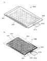
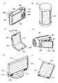
本発明の一態様に係る表示装置を用いることができる電子機器として、表示機器、パーソナルコンピュータ、記録媒体を備えた画像記憶装置または画像再生装置、携帯電話、携帯型を含むゲーム機、携帯データ端末、電子書籍端末、ビデオカメラ、デジタルスチルカメラ等のカメラ、ゴーグル型ディスプレイ(ヘッドマウントディスプレイ)、ナビゲーションシステム、音響再生装置(カーオーディオ、デジタルオーディオプレイヤー等)、複写機、ファクシミリ、プリンタ、プリンタ複合機、現金自動預け入れ払い機(ATM)、自動販売機などが挙げられる。これら電子機器の具体例を図23に示す。
Claims (9)
- 第1のノードと、第2のノードと、第3のノードと、表示素子と、が設けられた画素を有し、
前記第1のノードおよび前記第2のノードに第1のデータを書き込む機能と、
前記第2のノードに保持されている前記第1のデータを前記第3のノードに読み出す機能と、
前記第1のノードに保持されている前記第1のデータと前記第3のノードに読み出された前記第1のデータとの容量結合によって前記第1のノードに第2のデータを生成する機能と、
前記第2のデータを前記表示素子に供給して表示を行う機能と、
を有する表示装置。 - 第1の画素と、第2の画素と、第1の配線と、第2の配線と、を有し、
前記第1の画素および前記第2の画素のそれぞれには、第1のノードと、第2のノードと、第3のノードと、表示素子と、が設けられ、
前記第1の配線は前記第1の画素と電気的に接続され、
前記第2の配線は前記第1の画素と電気的に接続され、
前記第2の配線は前記第2の画素と電気的に接続され、
前記第1のノードおよび前記第2のノードに第1のデータを書き込む第1の機能と、
前記第2のノードに保持されている前記第1のデータを前記第3のノードに読み出す第2の機能と、
前記第1のノードに保持されている前記第1のデータと前記第3のノードに読み出された前記第1のデータとの容量結合によって、前記第1のノードに第2のデータを生成する第3の機能と、
前記第2のデータを前記表示素子に供給して表示を行う第4の機能と、を有し、
前記第1の配線に第1の信号が供給されたとき、前記第1の画素では前記第1の機能が働き、
前記第2の配線に第2の信号が供給されたとき、前記第1の画素では前記第2乃至前記第4の機能が働き、前記第2の画素では前記第1の機能が働く表示装置。 - 第1の画素と、第2の画素と、第1の配線と、第2の配線と、第3の配線と、第4の配線と、を有し、
前記第1の画素および前記第2の画素は、第1のトランジスタと、第2のトランジスタと、第3のトランジスタと、第4のトランジスタと、第1の容量素子と、第2の容量素子と、回路ブロックと、を有し、
前記第1のトランジスタのソースまたはドレインの一方は、前記第1の容量素子の一方の電極と電気的に接続され、
前記第1の容量素子の一方の電極は、前記第2のトランジスタのソースまたはドレインの一方と電気的に接続され、
前記第2のトランジスタのソースまたはドレインの他方は、前記第3のトランジスタのソースまたはドレインの一方と電気的に接続され、
前記第3のトランジスタのソースまたはドレインの一方は、前記第2の容量素子の一方の電極と電気的に接続され、
前記第2の容量素子の他方の電極は、前記第4のトランジスタのソースまたはドレインの一方と電気的に接続され、
前記第4のトランジスタのソースまたはドレインの一方は、前記回路ブロックと電気的に接続され、
前記第1の画素において、
前記第1のトランジスタのソースまたはドレインの他方は、前記第1の配線に電気的に接続され、
前記第4のトランジスタのソースまたはドレインの他方は、前記第1の配線に電気的に接続され、
前記第1のトランジスタのゲートは、前記第2の配線と電気的に接続され、
前記第2のトランジスタのゲートは、前記第3の配線と電気的に接続され、
前記第3のトランジスタのゲートは、前記第2の配線と電気的に接続され、
前記第4のトランジスタのゲートは、前記第2の配線と電気的に接続され、
前記第2の画素において、
前記第1のトランジスタのソースまたはドレインの他方は、前記第1の配線に電気的に接続され、
前記第4のトランジスタのソースまたはドレインの他方は、前記第1の配線に電気的に接続され、
前記第1のトランジスタのゲートは、前記第3の配線と電気的に接続され、
前記第2のトランジスタのゲートは、前記第4の配線と電気的に接続され、
前記第3のトランジスタのゲートは、前記第3の配線と電気的に接続され、
前記第4のトランジスタのゲートは、前記第3の配線と電気的に接続され、
前記回路ブロックは、表示素子を有する表示装置。 - 請求項3において、
前記回路ブロックは、第5のトランジスタと、第6のトランジスタと、第3の容量素子と、前記表示素子として有機EL素子と、を有し、
前記有機EL素子の一方の電極は、前記第6のトランジスタのソースまたはドレインの一方と電気的に接続され、
前記第6のトランジスタのソースまたはドレインの他方は、前記第3の容量素子の一方の電極と電気的に接続され、
前記第3の容量素子の一方の電極は、前記第5のトランジスタのソースまたはドレインの一方と電気的に接続され、
前記第5のトランジスタのゲートは、前記第3の容量素子の他方の電極と電気的に接続され、
前記第3の容量素子の他方の電極は、前記第2の容量素子の他方の電極と電気的に接続されている表示装置。 - 請求項4において、
前記第5のトランジスタのソースまたはドレインの他方は、前記第3のトランジスタのソースまたはドレインの他方と電気的に接続されている表示装置。 - 請求項3において、
前記回路ブロックは、第7のトランジスタと、第4の容量素子と、前記表示素子として液晶素子と、を有し、
前記液晶素子の一方の電極は、前記第4の容量素子の一方の電極と電気的に接続され、
前記第4の容量素子の一方の電極は、前記第7のトランジスタのソースまたはドレインの一方と電気的に接続され、
前記第7のトランジスタのソースまたはドレインの他方は、前記第2の容量素子の他方の電極と電気的に接続されている表示装置。 - 請求項6において、
前記第4の容量素子の他方の電極は、前記第3のトランジスタのソースまたはドレインの他方と電気的に接続されている表示装置。 - 請求項3乃至7のいずれか一項において、
前記第4のトランジスタは、チャネル形成領域に金属酸化物を有し、前記金属酸化物は、Inと、Znと、M(MはAl、Ti、Ga、Ge、Sn、Y、Zr、La、Ce、NdまたはHf)と、を有する表示装置。 - 請求項1乃至8のいずれか一項に記載の表示装置と、カメラと、を有する電子機器。
Priority Applications (6)
| Application Number | Priority Date | Filing Date | Title |
|---|---|---|---|
| CN201980017023.4A CN111837172A (zh) | 2018-03-06 | 2019-02-26 | 显示装置以及电子设备 |
| KR1020207028015A KR20200126408A (ko) | 2018-03-06 | 2019-02-26 | 표시 장치 및 전자 기기 |
| JP2020504472A JP7246365B2 (ja) | 2018-03-06 | 2019-02-26 | 表示装置および電子機器 |
| US16/977,937 US11204533B2 (en) | 2018-03-06 | 2019-02-26 | Display device and electronic device |
| US17/552,641 US11822198B2 (en) | 2018-03-06 | 2021-12-16 | Display device and electronic device |
| JP2023039283A JP2023073280A (ja) | 2018-03-06 | 2023-03-14 | 表示装置 |
Applications Claiming Priority (2)
| Application Number | Priority Date | Filing Date | Title |
|---|---|---|---|
| JP2018039185 | 2018-03-06 | ||
| JP2018-039185 | 2018-03-06 |
Related Child Applications (2)
| Application Number | Title | Priority Date | Filing Date |
|---|---|---|---|
| US16/977,937 A-371-Of-International US11204533B2 (en) | 2018-03-06 | 2019-02-26 | Display device and electronic device |
| US17/552,641 Continuation US11822198B2 (en) | 2018-03-06 | 2021-12-16 | Display device and electronic device |
Publications (1)
| Publication Number | Publication Date |
|---|---|
| WO2019171204A1 true WO2019171204A1 (ja) | 2019-09-12 |
Family
ID=67846964
Family Applications (1)
| Application Number | Title | Priority Date | Filing Date |
|---|---|---|---|
| PCT/IB2019/051513 WO2019171204A1 (ja) | 2018-03-06 | 2019-02-26 | 表示装置および電子機器 |
Country Status (5)
| Country | Link |
|---|---|
| US (2) | US11204533B2 (ja) |
| JP (2) | JP7246365B2 (ja) |
| KR (1) | KR20200126408A (ja) |
| CN (1) | CN111837172A (ja) |
| WO (1) | WO2019171204A1 (ja) |
Families Citing this family (1)
| Publication number | Priority date | Publication date | Assignee | Title |
|---|---|---|---|---|
| KR20210027110A (ko) | 2019-08-29 | 2021-03-10 | 가부시키가이샤 한도오따이 에네루기 켄큐쇼 | 표시 장치 |
Citations (10)
| Publication number | Priority date | Publication date | Assignee | Title |
|---|---|---|---|---|
| US6107980A (en) * | 1998-02-27 | 2000-08-22 | Geo-Centers, Inc. | Cell circuit for active matrix liquid crystal displays using high polarization, analog response liquid crystals |
| JP2001281634A (ja) * | 2000-03-31 | 2001-10-10 | Canon Inc | 液晶素子の駆動方法 |
| JP2002277898A (ja) * | 2001-01-09 | 2002-09-25 | Sharp Corp | 電子装置およびその駆動方法 |
| JP2009037230A (ja) * | 2007-07-11 | 2009-02-19 | Semiconductor Energy Lab Co Ltd | アクティブマトリクス型表示装置及びそれを用いた電子機器 |
| JP2009109600A (ja) * | 2007-10-29 | 2009-05-21 | Hitachi Displays Ltd | 液晶表示装置 |
| JP2009128900A (ja) * | 2007-11-26 | 2009-06-11 | Samsung Electronics Co Ltd | 液晶表示装置 |
| JP2011145447A (ja) * | 2010-01-14 | 2011-07-28 | Seiko Epson Corp | 表示素子駆動回路、電気光学装置及び電子機器 |
| US20120249509A1 (en) * | 2011-03-29 | 2012-10-04 | Samsung Electronics Co., Ltd. | Pixel circuit and method of operating the same |
| JP2016206659A (ja) * | 2015-04-16 | 2016-12-08 | 株式会社半導体エネルギー研究所 | 表示装置および電子機器、並びに表示装置の駆動方法 |
| JP2017134240A (ja) * | 2016-01-28 | 2017-08-03 | セイコーエプソン株式会社 | 電気光学装置、及び、電気光学装置の制御方法 |
Family Cites Families (20)
| Publication number | Priority date | Publication date | Assignee | Title |
|---|---|---|---|---|
| JPH0470820A (ja) * | 1990-07-12 | 1992-03-05 | Matsushita Electric Ind Co Ltd | アクティブ・マトリックス型平板表示装置 |
| JP2001282201A (ja) | 2000-03-31 | 2001-10-12 | Internatl Business Mach Corp <Ibm> | 表示装置、液晶表示パネル、液晶表示装置および液晶表示装置の駆動方法 |
| JP5078246B2 (ja) | 2005-09-29 | 2012-11-21 | 株式会社半導体エネルギー研究所 | 半導体装置、及び半導体装置の作製方法 |
| EP1995787A3 (en) | 2005-09-29 | 2012-01-18 | Semiconductor Energy Laboratory Co, Ltd. | Semiconductor device having oxide semiconductor layer and manufacturing method therof |
| JP5587336B2 (ja) | 2008-12-31 | 2014-09-10 | イー・アイ・デュポン・ドウ・ヌムール・アンド・カンパニー | 曇り度が低く防水性の高いアイオノマー組成物及びそれを含む物品 |
| CN102598249B (zh) | 2009-10-30 | 2014-11-05 | 株式会社半导体能源研究所 | 半导体装置 |
| JP2011150009A (ja) | 2010-01-19 | 2011-08-04 | Seiko Epson Corp | 電気光学装置、電気光学装置の駆動方法、電子機器 |
| JP2011150010A (ja) | 2010-01-19 | 2011-08-04 | Seiko Epson Corp | 電気光学装置、電気光学装置の駆動方法、電子機器 |
| JP2012145655A (ja) | 2011-01-07 | 2012-08-02 | Canon Inc | 画像表示装置及びその制御方法 |
| JP2012168226A (ja) | 2011-02-10 | 2012-09-06 | Seiko Epson Corp | 電気光学装置の駆動回路、電気光学装置及び電子機器 |
| JP5804732B2 (ja) | 2011-03-04 | 2015-11-04 | 株式会社Joled | 駆動方法、表示装置および電子機器 |
| KR20120120761A (ko) * | 2011-04-25 | 2012-11-02 | 삼성디스플레이 주식회사 | 액정 표시 장치 |
| KR20130133501A (ko) * | 2012-05-29 | 2013-12-09 | 삼성디스플레이 주식회사 | 평판표시장치 |
| JP6394171B2 (ja) * | 2013-10-30 | 2018-09-26 | 株式会社リコー | 電界効果型トランジスタ、表示素子、画像表示装置、及びシステム |
| US10140940B2 (en) | 2015-07-24 | 2018-11-27 | Japan Display Inc. | Display device |
| JP2017027012A (ja) | 2015-07-24 | 2017-02-02 | 株式会社ジャパンディスプレイ | 表示装置 |
| KR20200053522A (ko) | 2017-09-14 | 2020-05-18 | 가부시키가이샤 한도오따이 에네루기 켄큐쇼 | 이차 전지의 이상 검지 시스템 및 이차 전지의 이상 검출 방법 |
| CN111052213A (zh) | 2017-09-15 | 2020-04-21 | 株式会社半导体能源研究所 | 显示装置及电子设备 |
| WO2019087010A1 (ja) | 2017-11-02 | 2019-05-09 | 株式会社半導体エネルギー研究所 | 給電装置及び電子機器、並びに給電装置の動作方法 |
| JP7245788B2 (ja) | 2018-02-01 | 2023-03-24 | 株式会社半導体エネルギー研究所 | 表示装置 |
-
2019
- 2019-02-26 CN CN201980017023.4A patent/CN111837172A/zh active Pending
- 2019-02-26 JP JP2020504472A patent/JP7246365B2/ja active Active
- 2019-02-26 KR KR1020207028015A patent/KR20200126408A/ko not_active Application Discontinuation
- 2019-02-26 WO PCT/IB2019/051513 patent/WO2019171204A1/ja active Application Filing
- 2019-02-26 US US16/977,937 patent/US11204533B2/en active Active
-
2021
- 2021-12-16 US US17/552,641 patent/US11822198B2/en active Active
-
2023
- 2023-03-14 JP JP2023039283A patent/JP2023073280A/ja active Pending
Patent Citations (10)
| Publication number | Priority date | Publication date | Assignee | Title |
|---|---|---|---|---|
| US6107980A (en) * | 1998-02-27 | 2000-08-22 | Geo-Centers, Inc. | Cell circuit for active matrix liquid crystal displays using high polarization, analog response liquid crystals |
| JP2001281634A (ja) * | 2000-03-31 | 2001-10-10 | Canon Inc | 液晶素子の駆動方法 |
| JP2002277898A (ja) * | 2001-01-09 | 2002-09-25 | Sharp Corp | 電子装置およびその駆動方法 |
| JP2009037230A (ja) * | 2007-07-11 | 2009-02-19 | Semiconductor Energy Lab Co Ltd | アクティブマトリクス型表示装置及びそれを用いた電子機器 |
| JP2009109600A (ja) * | 2007-10-29 | 2009-05-21 | Hitachi Displays Ltd | 液晶表示装置 |
| JP2009128900A (ja) * | 2007-11-26 | 2009-06-11 | Samsung Electronics Co Ltd | 液晶表示装置 |
| JP2011145447A (ja) * | 2010-01-14 | 2011-07-28 | Seiko Epson Corp | 表示素子駆動回路、電気光学装置及び電子機器 |
| US20120249509A1 (en) * | 2011-03-29 | 2012-10-04 | Samsung Electronics Co., Ltd. | Pixel circuit and method of operating the same |
| JP2016206659A (ja) * | 2015-04-16 | 2016-12-08 | 株式会社半導体エネルギー研究所 | 表示装置および電子機器、並びに表示装置の駆動方法 |
| JP2017134240A (ja) * | 2016-01-28 | 2017-08-03 | セイコーエプソン株式会社 | 電気光学装置、及び、電気光学装置の制御方法 |
Also Published As
| Publication number | Publication date |
|---|---|
| US20220107538A1 (en) | 2022-04-07 |
| CN111837172A (zh) | 2020-10-27 |
| US11822198B2 (en) | 2023-11-21 |
| US11204533B2 (en) | 2021-12-21 |
| JP7246365B2 (ja) | 2023-03-27 |
| KR20200126408A (ko) | 2020-11-06 |
| JP2023073280A (ja) | 2023-05-25 |
| JPWO2019171204A1 (ja) | 2021-04-08 |
| US20210011347A1 (en) | 2021-01-14 |
Similar Documents
| Publication | Publication Date | Title |
|---|---|---|
| US11626082B2 (en) | Display device and electronic device | |
| WO2019207440A1 (ja) | 表示装置および電子機器 | |
| JP2024045230A (ja) | 表示装置 | |
| JP2024050929A (ja) | 表示装置 | |
| US11436993B2 (en) | Display apparatus and electronic device | |
| JP7374896B2 (ja) | 表示装置および電子機器 | |
| JP2023073280A (ja) | 表示装置 | |
| JP7315572B2 (ja) | 表示装置および電子機器 | |
| WO2020136494A1 (ja) | 表示装置および電子機器 | |
| JP7412360B2 (ja) | 表示装置および電子機器 | |
| WO2020240329A1 (ja) | 表示装置および電子機器 |
Legal Events
| Date | Code | Title | Description |
|---|---|---|---|
| 121 | Ep: the epo has been informed by wipo that ep was designated in this application |
Ref document number: 19763945 Country of ref document: EP Kind code of ref document: A1 |
|
| ENP | Entry into the national phase |
Ref document number: 2020504472 Country of ref document: JP Kind code of ref document: A |
|
| NENP | Non-entry into the national phase |
Ref country code: DE |
|
| ENP | Entry into the national phase |
Ref document number: 20207028015 Country of ref document: KR Kind code of ref document: A |
|
| 122 | Ep: pct application non-entry in european phase |
Ref document number: 19763945 Country of ref document: EP Kind code of ref document: A1 |