WO2019171198A1 - 半導体装置 - Google Patents
半導体装置 Download PDFInfo
- Publication number
- WO2019171198A1 WO2019171198A1 PCT/IB2019/051406 IB2019051406W WO2019171198A1 WO 2019171198 A1 WO2019171198 A1 WO 2019171198A1 IB 2019051406 W IB2019051406 W IB 2019051406W WO 2019171198 A1 WO2019171198 A1 WO 2019171198A1
- Authority
- WO
- WIPO (PCT)
- Prior art keywords
- transistor
- oxide
- conductor
- insulator
- region
- Prior art date
- Legal status (The legal status is an assumption and is not a legal conclusion. Google has not performed a legal analysis and makes no representation as to the accuracy of the status listed.)
- Ceased
Links
Images










Classifications
-
- H—ELECTRICITY
- H10—SEMICONDUCTOR DEVICES; ELECTRIC SOLID-STATE DEVICES NOT OTHERWISE PROVIDED FOR
- H10D—INORGANIC ELECTRIC SEMICONDUCTOR DEVICES
- H10D84/00—Integrated devices formed in or on semiconductor substrates that comprise only semiconducting layers, e.g. on Si wafers or on GaAs-on-Si wafers
- H10D84/80—Integrated devices formed in or on semiconductor substrates that comprise only semiconducting layers, e.g. on Si wafers or on GaAs-on-Si wafers characterised by the integration of at least one component covered by groups H10D12/00 or H10D30/00, e.g. integration of IGFETs
- H10D84/82—Integrated devices formed in or on semiconductor substrates that comprise only semiconducting layers, e.g. on Si wafers or on GaAs-on-Si wafers characterised by the integration of at least one component covered by groups H10D12/00 or H10D30/00, e.g. integration of IGFETs of only field-effect components
- H10D84/83—Integrated devices formed in or on semiconductor substrates that comprise only semiconducting layers, e.g. on Si wafers or on GaAs-on-Si wafers characterised by the integration of at least one component covered by groups H10D12/00 or H10D30/00, e.g. integration of IGFETs of only field-effect components of only insulated-gate FETs [IGFET]
-
- G—PHYSICS
- G09—EDUCATION; CRYPTOGRAPHY; DISPLAY; ADVERTISING; SEALS
- G09F—DISPLAYING; ADVERTISING; SIGNS; LABELS OR NAME-PLATES; SEALS
- G09F9/00—Indicating arrangements for variable information in which the information is built-up on a support by selection or combination of individual elements
- G09F9/30—Indicating arrangements for variable information in which the information is built-up on a support by selection or combination of individual elements in which the desired character or characters are formed by combining individual elements
-
- H—ELECTRICITY
- H10—SEMICONDUCTOR DEVICES; ELECTRIC SOLID-STATE DEVICES NOT OTHERWISE PROVIDED FOR
- H10B—ELECTRONIC MEMORY DEVICES
- H10B12/00—Dynamic random access memory [DRAM] devices
-
- H—ELECTRICITY
- H10—SEMICONDUCTOR DEVICES; ELECTRIC SOLID-STATE DEVICES NOT OTHERWISE PROVIDED FOR
- H10D—INORGANIC ELECTRIC SEMICONDUCTOR DEVICES
- H10D30/00—Field-effect transistors [FET]
- H10D30/60—Insulated-gate field-effect transistors [IGFET]
- H10D30/67—Thin-film transistors [TFT]
- H10D30/6729—Thin-film transistors [TFT] characterised by the electrodes
- H10D30/673—Thin-film transistors [TFT] characterised by the electrodes characterised by the shapes, relative sizes or dispositions of the gate electrodes
- H10D30/6733—Multi-gate TFTs
- H10D30/6734—Multi-gate TFTs having gate electrodes arranged on both top and bottom sides of the channel, e.g. dual-gate TFTs
-
- H—ELECTRICITY
- H10—SEMICONDUCTOR DEVICES; ELECTRIC SOLID-STATE DEVICES NOT OTHERWISE PROVIDED FOR
- H10D—INORGANIC ELECTRIC SEMICONDUCTOR DEVICES
- H10D30/00—Field-effect transistors [FET]
- H10D30/60—Insulated-gate field-effect transistors [IGFET]
- H10D30/67—Thin-film transistors [TFT]
- H10D30/674—Thin-film transistors [TFT] characterised by the active materials
- H10D30/6741—Group IV materials, e.g. germanium or silicon carbide
-
- H—ELECTRICITY
- H10—SEMICONDUCTOR DEVICES; ELECTRIC SOLID-STATE DEVICES NOT OTHERWISE PROVIDED FOR
- H10D—INORGANIC ELECTRIC SEMICONDUCTOR DEVICES
- H10D30/00—Field-effect transistors [FET]
- H10D30/60—Insulated-gate field-effect transistors [IGFET]
- H10D30/67—Thin-film transistors [TFT]
- H10D30/674—Thin-film transistors [TFT] characterised by the active materials
- H10D30/6755—Oxide semiconductors, e.g. zinc oxide, copper aluminium oxide or cadmium stannate
-
- H—ELECTRICITY
- H10—SEMICONDUCTOR DEVICES; ELECTRIC SOLID-STATE DEVICES NOT OTHERWISE PROVIDED FOR
- H10D—INORGANIC ELECTRIC SEMICONDUCTOR DEVICES
- H10D62/00—Semiconductor bodies, or regions thereof, of devices having potential barriers
- H10D62/80—Semiconductor bodies, or regions thereof, of devices having potential barriers characterised by the materials
-
- H—ELECTRICITY
- H10—SEMICONDUCTOR DEVICES; ELECTRIC SOLID-STATE DEVICES NOT OTHERWISE PROVIDED FOR
- H10D—INORGANIC ELECTRIC SEMICONDUCTOR DEVICES
- H10D64/00—Electrodes of devices having potential barriers
- H10D64/01—Manufacture or treatment
- H10D64/017—Manufacture or treatment using dummy gates in processes wherein at least parts of the final gates are self-aligned to the dummy gates, i.e. replacement gate processes
-
- H—ELECTRICITY
- H10—SEMICONDUCTOR DEVICES; ELECTRIC SOLID-STATE DEVICES NOT OTHERWISE PROVIDED FOR
- H10D—INORGANIC ELECTRIC SEMICONDUCTOR DEVICES
- H10D84/00—Integrated devices formed in or on semiconductor substrates that comprise only semiconducting layers, e.g. on Si wafers or on GaAs-on-Si wafers
-
- H—ELECTRICITY
- H10—SEMICONDUCTOR DEVICES; ELECTRIC SOLID-STATE DEVICES NOT OTHERWISE PROVIDED FOR
- H10D—INORGANIC ELECTRIC SEMICONDUCTOR DEVICES
- H10D84/00—Integrated devices formed in or on semiconductor substrates that comprise only semiconducting layers, e.g. on Si wafers or on GaAs-on-Si wafers
- H10D84/01—Manufacture or treatment
- H10D84/0123—Integrating together multiple components covered by H10D12/00 or H10D30/00, e.g. integrating multiple IGBTs
- H10D84/0126—Integrating together multiple components covered by H10D12/00 or H10D30/00, e.g. integrating multiple IGBTs the components including insulated gates, e.g. IGFETs
-
- H—ELECTRICITY
- H10—SEMICONDUCTOR DEVICES; ELECTRIC SOLID-STATE DEVICES NOT OTHERWISE PROVIDED FOR
- H10D—INORGANIC ELECTRIC SEMICONDUCTOR DEVICES
- H10D84/00—Integrated devices formed in or on semiconductor substrates that comprise only semiconducting layers, e.g. on Si wafers or on GaAs-on-Si wafers
- H10D84/01—Manufacture or treatment
- H10D84/02—Manufacture or treatment characterised by using material-based technologies
- H10D84/03—Manufacture or treatment characterised by using material-based technologies using Group IV technology, e.g. silicon technology or silicon-carbide [SiC] technology
- H10D84/038—Manufacture or treatment characterised by using material-based technologies using Group IV technology, e.g. silicon technology or silicon-carbide [SiC] technology using silicon technology, e.g. SiGe
-
- H—ELECTRICITY
- H10—SEMICONDUCTOR DEVICES; ELECTRIC SOLID-STATE DEVICES NOT OTHERWISE PROVIDED FOR
- H10P—GENERIC PROCESSES OR APPARATUS FOR THE MANUFACTURE OR TREATMENT OF DEVICES COVERED BY CLASS H10
- H10P14/00—Formation of materials, e.g. in the shape of layers or pillars
- H10P14/20—Formation of materials, e.g. in the shape of layers or pillars of semiconductor materials
- H10P14/34—Deposited materials, e.g. layers
- H10P14/3402—Deposited materials, e.g. layers characterised by the chemical composition
- H10P14/3434—Deposited materials, e.g. layers characterised by the chemical composition being oxide semiconductor materials
Definitions
- One embodiment of the present invention relates to a semiconductor material and a semiconductor device.
- a semiconductor device refers to all devices that can function by utilizing semiconductor characteristics.
- a semiconductor element such as a transistor, a semiconductor circuit, an arithmetic device, and a memory device are one embodiment of the semiconductor device.
- a display device (a liquid crystal display device, a light-emitting display device, or the like), a projection device, a lighting device, an electro-optical device, a power storage device, a memory device, a semiconductor circuit, an imaging device, an electronic device, or the like may have a semiconductor device. .
- one embodiment of the present invention is not limited to the above technical field.
- One embodiment of the invention disclosed in this specification and the like relates to an object, a method, or a manufacturing method.
- one embodiment of the present invention relates to a process, a machine, a manufacture, or a composition (composition of matter).
- oxide semiconductors As a semiconductor thin film applicable to a transistor, a silicon-based semiconductor material is widely known, but an oxide semiconductor has attracted attention as another material.
- oxide semiconductors for example, not only single-component metal oxides such as indium oxide and zinc oxide but also multi-component metal oxides are known.
- IGZO In—Ga—Zn oxide
- Non-Patent Document 1 and Non-Patent Document 2 also disclose a technique for manufacturing a transistor using an oxide semiconductor having a CAAC structure. Furthermore, Non-Patent Document 4 and Non-Patent Document 5 show that even an oxide semiconductor having lower crystallinity than the CAAC structure and the nc structure has a minute crystal.
- Non-Patent Document 6 a transistor using IGZO as an active layer has extremely low off-state current (see Non-Patent Document 6), and an LSI and a display using the characteristics have been reported (see Non-Patent Document 7 and Non-Patent Document 8). .
- One of the problems is to suppress the charging phenomenon that leads to dielectric breakdown.
- the thickness of various insulating films such as a gate insulating film is reduced, so that dielectric breakdown due to abnormal charging is a more serious problem.
- An object of one embodiment of the present invention is to provide a semiconductor device capable of retaining data for a long period of time.
- An object of one embodiment of the present invention is to provide a semiconductor device in which electrical characteristics and reliability of a transistor including an oxide semiconductor are stable.
- An object of one embodiment of the present invention is to provide a semiconductor device having favorable electrical characteristics.
- An object of one embodiment of the present invention is to provide a semiconductor device that can be miniaturized or highly integrated.
- An object of one embodiment of the present invention is to provide a semiconductor device with high productivity.
- An object of one embodiment of the present invention is to provide a semiconductor device with high design freedom.
- An object of one embodiment of the present invention is to provide a semiconductor device capable of suppressing power consumption.
- An object of one embodiment of the present invention is to provide a semiconductor device with high information writing speed.
- An object of one embodiment of the present invention is to provide a novel semiconductor device.
- One embodiment of the present invention is a semiconductor device including a first region and a second region on the same plane, the first region including a transistor, and the second region including a dummy transistor.
- the transistor includes: a first wiring layer; a semiconductor layer including an oxide disposed above the first wiring layer; a second wiring layer disposed above the semiconductor layer; And a dummy transistor is selected from the first wiring layer, the second wiring layer, the semiconductor layer, and the third wiring layer. Have the same area as the one or more.
- One embodiment of the present invention includes a first region and a second region over a substrate, the first region includes a plurality of first transistors and dummy transistors, and the second region includes The pattern density of the plurality of second transistors and the combination of the first transistor and the dummy transistor in the first region is equal to the pattern density of the second transistor in the second region.
- the first transistor and the second transistor have the same structure, and the structure included in the first transistor is made of the same material as the structure included in the dummy transistor and is disposed in the same layer. .
- the first transistor includes a first oxide and a first conductor
- the dummy transistor includes a second oxide
- the first transistor and the dummy transistor are adjacent to each other.
- the first conductor has a region overlapping with the first oxide and the second oxide.
- the first conductor is in contact with the first oxide and the second oxide.
- the first transistor includes a first oxide
- the first oxide includes a high resistance region and a low resistance region
- the dummy transistor includes a second oxide.
- the resistance of the second oxide is reduced.
- each of the first oxide and the second oxide includes In, an element M (M is Al, Ga, Y, or Sn), and Zn.
- a semiconductor device in which variations in electrical characteristics and shape are suppressed in a plurality of elements can be provided.
- a semiconductor device in which deterioration of elements or dielectric breakdown is suppressed can be provided.
- a semiconductor device in which electrical characteristics and reliability of a transistor including an oxide semiconductor are stable can be provided.
- a semiconductor device capable of holding data for a long period can be provided.
- a semiconductor device having favorable electrical characteristics can be provided.
- a semiconductor device that can be miniaturized or highly integrated can be provided.
- a highly productive semiconductor device can be provided.
- a semiconductor device with high design freedom can be provided.
- a semiconductor device with high information writing speed can be provided.
- a semiconductor device that can reduce power consumption can be provided.
- a novel semiconductor device can be provided.
- 4A and 4B are a top view and a cross-sectional view of a semiconductor device according to one embodiment of the present invention.
- 4A and 4B are a top view and a cross-sectional view of a semiconductor device according to one embodiment of the present invention.
- 4A and 4B are a top view and a cross-sectional view of a semiconductor device according to one embodiment of the present invention.
- 4A and 4B are a top view and a cross-sectional view of a semiconductor device according to one embodiment of the present invention.
- 4A and 4B are a top view and a cross-sectional view of a semiconductor device according to one embodiment of the present invention.
- 4A and 4B are a top view and a cross-sectional view of a semiconductor device according to one embodiment of the present invention.
- FIG. 4A and 4B are a top view and a cross-sectional view of a semiconductor device according to one embodiment of the present invention.
- FIG. 6 is a cross-sectional view of a semiconductor device according to one embodiment of the present invention.
- 6A and 6B illustrate a structural example of a transistor according to one embodiment of the present invention.
- 6A and 6B illustrate a structural example of a transistor according to one embodiment of the present invention.
- 6A and 6B illustrate a structural example of a transistor according to one embodiment of the present invention.
- 6A and 6B illustrate a structural example of a transistor according to one embodiment of the present invention.
- 6A and 6B illustrate a structural example of a transistor according to one embodiment of the present invention.
- FIG. 6A and 6B illustrate a structural example of a transistor according to one embodiment of the present invention.
- FIG. 10 is a block diagram illustrating a structure example of a memory device according to one embodiment of the present invention.
- FIG. 10 is a circuit diagram illustrating a structural example of a memory device according to one embodiment of the present invention.
- FIG. 10 is a schematic view of a semiconductor device according to one embodiment of the present invention.
- FIG. 3 is a schematic diagram of a memory device according to one embodiment of the present invention.
- 10A and 10B each illustrate an example of a display device and a circuit configuration example of a pixel.
- 8A and 8B illustrate a circuit configuration example of a pixel.
- FIG. 6 illustrates a configuration example of a driver circuit.
- FIG. 6 illustrates a configuration example of a driver circuit.
- FIG. 6 illustrates an example of a display device.
- FIG. 6 illustrates an example of a display device.
- FIG. 6 illustrates an example of a display module.
- FIG. 14 illustrates an electronic device according to one embodiment of the present invention.
- 4A and 4B illustrate a structure of a semiconductor device according to an embodiment.
- 3A and 3B illustrate a structure and electrical characteristics of a semiconductor device according to an embodiment.
- 3A and 3B illustrate a structure and electrical characteristics of a semiconductor device according to an embodiment.
- 3A and 3B illustrate a structure and electrical characteristics of a semiconductor device according to an embodiment.
- 6A and 6B illustrate electrical characteristics of a semiconductor device according to an embodiment.
- a transistor is an element having at least three terminals including a gate, a drain, and a source.
- a channel is formed between the drain (drain terminal, drain region or drain electrode) and the source (source terminal, source region or source electrode), and the region and source where the drain and channel are formed.
- a current can be passed through the.
- a region where a channel is formed refers to a region where current mainly flows.
- the functions of the source and drain may be switched when transistors with different polarities are used or when the direction of current changes during circuit operation. Therefore, in this specification and the like, the terms source and drain can be used interchangeably.
- “electrically connected” includes a case of being connected via “something having an electric action”.
- the “thing having some electric action” is not particularly limited as long as it can exchange electric signals between connection targets.
- “thing having some electric action” includes electrodes, wiring, switching elements such as transistors, resistance elements, inductors, capacitors, and other elements having various functions.
- a nitrided oxide refers to a compound having a higher nitrogen content than oxygen.
- oxynitride refers to a compound having a higher oxygen content than nitrogen.
- content of each element can be measured using Rutherford backscattering method (RBS: Rutherford Backscattering Spectrometry) etc., for example.
- parallel means a state in which two straight lines are arranged at an angle of ⁇ 10 ° to 10 °. Therefore, the case of ⁇ 5 ° to 5 ° is also included.
- substantially parallel means a state in which two straight lines are arranged at an angle of ⁇ 30 ° to 30 °.
- Vertical refers to a state in which two straight lines are arranged at an angle of 80 ° to 100 °. Therefore, the case of 85 ° to 95 ° is also included.
- substantially vertical means a state in which two straight lines are arranged at an angle of 60 ° to 120 °.
- a barrier film refers to a film having a function of suppressing permeation of impurities such as hydrogen or oxygen, and when the barrier film has conductivity, the barrier film is referred to as a conductive barrier film.
- impurities such as hydrogen or oxygen
- normally on characteristic of a transistor means that the transistor is on when no potential is applied by a power supply (0 V).
- normally-on characteristics of a transistor may refer to an electric characteristic in which a current (Id) flows between a drain and a source when a voltage (Vg) applied to the gate of the transistor is 0V.
- an oxide semiconductor is a kind of metal oxide.
- a metal oxide refers to an oxide having a metal element. Metal oxides may exhibit insulating properties, semiconductivity, and conductivity depending on the composition and formation method.
- a metal oxide exhibiting semiconductivity is referred to as a metal oxide semiconductor or an oxide semiconductor (also referred to as an oxide semiconductor or simply OS).
- a metal oxide exhibiting insulating properties is referred to as a metal oxide insulator or an oxide insulator.
- a metal oxide exhibiting conductivity is referred to as a metal oxide conductor or an oxide conductor. That is, a metal oxide used for a channel formation region or the like of a transistor can be called an oxide semiconductor.
- Examples of the element using the oxide semiconductor include a switching element (such as a transistor), a capacitor element, an inductance element, a memory element, a display element (such as a light emitting element), and the like.
- a metal oxide containing indium is preferably used.
- an In-M-Zn oxide (the element M is aluminum, gallium, yttrium, copper, vanadium, beryllium, boron, titanium, iron, nickel, germanium, zirconium, molybdenum, lanthanum, hafnium, tantalum, tungsten, or magnesium.
- a metal oxide such as one or more selected from the above can be used.
- an In—Ga oxide or an In—Zn oxide may be used as the oxide semiconductor.
- a transistor using an oxide semiconductor in a region where a channel is formed has a very small leakage current in a non-conduction state, so that a semiconductor device with low power consumption can be provided.
- an oxide semiconductor various elements can be stacked and three-dimensionally integrated.
- an oxide semiconductor can be formed by a sputtering method or the like, a three-dimensional integrated circuit (three-dimensional integrated circuit) in which a circuit is developed not only on the plane of the substrate but also in the vertical direction is used. Can do.
- a transistor including an oxide semiconductor has a normally-on characteristic (a voltage is applied to the gate electrode) due to impurities (typically hydrogen, water, and the like) in the oxide semiconductor and oxygen vacancies. Even if it is not applied, a channel is present and a current flows through the transistor). In addition, when the transistor is driven in an oxide semiconductor with excess oxygen exceeding an appropriate amount, the valence of excess oxygen changes, and the electrical characteristics of the transistor fluctuate. , Reliability may be worse.
- an oxide semiconductor used for the transistor is a high-purity intrinsic oxide semiconductor which does not have impurities, oxygen vacancies, and oxygen more than stoichiometric composition (hereinafter also referred to as excess oxygen). It is preferable.
- oxygen in the oxide semiconductor is absorbed by a conductor included in the transistor or a conductor used for a plug or a wiring connected to the transistor. May cause defects.
- oxygen in the oxide semiconductor may be absorbed by a conductor included in the transistor by the heat treatment.
- oxygen deficiency may occur in the oxide semiconductor due to process damage in manufacturing the transistor. Further, oxygen in the oxide semiconductor is absorbed by a conductor included in the transistor or a plug or wiring connected to the transistor due to a heating step or the like at the time of manufacturing the transistor, and the oxide semiconductor Oxygen deficiency may occur.
- the oxide preferably has a region where oxygen is present in excess of the stoichiometric composition (hereinafter also referred to as an excess oxygen region).
- an excess oxygen region is preferably provided in an interlayer film or the like located above and below the transistor.
- oxygen vacancies in the oxide semiconductor can be compensated for by diffusing excess oxygen in the structure having the excess oxygen region into oxygen vacancies generated in the oxide semiconductor.
- excess oxygen in the structure including the excess oxygen region diffuses beyond an appropriate amount, the excessively supplied oxygen may change the structure of the oxide semiconductor.
- a plurality of circuits having different functions may be arranged on the same substrate.
- the density of necessary elements or wirings constituting the circuit varies depending on the required circuit configuration. Specifically, in a circuit region that is regularly arranged and highly integrated, represented by a memory cell, a pixel region, and the like, and a circuit region whose layout is determined as necessary, such as a drive circuit and a correction circuit, elements and wiring A difference in density occurs in the arrangement (hereinafter also referred to as a layout in the circuit area).
- FIG. 5A is a top view of the semiconductor device.
- FIG. 5B is a cross-sectional view taken along dashed-dotted line A1-A2 in FIG. In FIG. 5, some elements are omitted for clarity of illustration.
- the substrate 10 has a region 12 and a region 11.
- Region 12 has elements 16 arranged at a low density.
- the region 11 has a plurality of elements 16 arranged at high density. Note that an element 16 in the drawing is a simplified element having an oxide semiconductor.
- a structure 13 including an oxide containing more oxygen than the stoichiometric composition is disposed.
- the amount of oxygen diffused into one device 16 between the device 16 disposed in the region 12 and the plurality of devices 16 disposed in the region 11. May be different.
- the excess oxygen region of the structure 13 is designed on the basis of the characteristics of the element 16 in the region 12
- the element 16 in the region 11 has a high probability that the excess oxygen is insufficient.
- the excess oxygen region of the structure 13 is designed on the basis of the characteristics of the element 16 in the region 11, the element 16 in the region 12 has a high probability that excess oxygen will diffuse beyond an appropriate amount.
- an element including an oxide semiconductor when the elements are arranged at different densities, there is a problem that it is difficult to uniformly control the excess oxygen region.
- the structure 13 In order to solve the above problem, it is conceivable to make the structure 13 separately in the region 11 and the region 12.
- the number of steps increases, and in particular, the number of steps accompanied by heat treatment that promotes diffusion of excess oxygen increases, thereby making the process design complicated.
- process damage in manufacturing a transistor increases, and oxygen vacancies may be generated in the oxide semiconductor.
- each structure of the element can be manufactured by repeatedly performing film formation using a material suitable for each structure and processing and forming the film.
- the film is formed by, for example, a sputtering method, a chemical vapor deposition (CVD) method, a molecular beam epitaxy (MBE) method, a pulsed laser deposition (PLD: Pulsed Laser Deposition) method, or an ALDAtom (ALDA) method. Film formation is performed using a Layer Deposition method or the like.
- CVD chemical vapor deposition
- MBE molecular beam epitaxy
- PLD Pulsed Laser Deposition
- ALDAtom ALDA
- the CVD method can be classified into a plasma CVD (PECVD: Plasma Enhanced CVD) method using plasma, a thermal CVD (TCVD: Thermal CVD) method using heat, and a photo CVD (Photo CVD) method using light. Furthermore, it can be divided into a metal CVD (MCVD: Metal CVD) method and an organic metal CVD (MOCVD: Metal Organic CVD) method depending on the source gas used.
- PECVD Plasma Enhanced CVD
- TCVD Thermal CVD
- Photo CVD Photo CVD
- MCVD Metal CVD
- MOCVD Metal Organic CVD
- the plasma CVD method can obtain a high-quality film at a relatively low temperature.
- wiring, electrodes, elements (transistors, capacitors, etc.) included in a semiconductor device may receive a charge from plasma generated at the time of film formation to cause a charging phenomenon (charging state). This is also known as charging up.)
- a wiring, an electrode, an element, or the like included in the semiconductor device may be destroyed by the accumulated charge.
- each wiring is likely to be in an electrically floating state by dividing the wiring.
- Each wiring after being divided is charged up even in a later process, and causes electrostatic breakdown (ESD) of the element.
- ESD electrostatic breakdown
- each electrode of the transistor is charged with a different potential, there is a high probability that the gate insulator is destroyed.
- the number of film forming steps and processing steps for the film increases as the vertical integration degree increases. That is, the probability of electrostatic breakdown due to charge-up tends to increase in proportion to the number of film forming steps and the number of steps for forming the film.
- the plasma is uniformly distributed on the substrate. If a uniform plasma charge is induced on the substrate, one of the elements in the element layout region arranged at a high density and one of the elements in the element layout region arranged at a low density There is a problem that the charge amount is different.
- FIG. 7A is a top view of the semiconductor device.
- 7B and 7C are cross-sectional views taken along dashed-dotted line A1-A2 in FIG. 7A. In FIG. 7, some elements are omitted for clarity of illustration.
- the substrate 10 has a region 12 and a region 11.
- Region 12 has elements 16 arranged at a low density.
- the region 11 has a plurality of elements 16 arranged at high density. Note that an element 16 in the drawing is a simplified element having an oxide semiconductor.
- FIG. 7B schematically shows a process of forming a film 15 that is a structure constituting the element 16 over the substrate 10 and processing the film 15 by a dry etching method using the mask 17.
- FIG. 7C schematically shows a state where the film 15 is divided by the processing. A plurality of elements 16 are formed by dividing the film 15.
- ions accelerated by the plasma 19 selectively remove a part of the film 15 by sputtering and removing the surface of the film 15.
- the film 15 is a conductive film
- the film 15 has a uniform potential while being exposed to plasma.
- the film 15 is divided to form a plurality of elements 16.
- the amount of plasma charge per element 16 in the region 11 is smaller than that in the region 12. That is, the element 16 disposed in the region 12 is charged up, and the probability of causing electrostatic breakdown of the element 16 increases.
- the charge-up that occurs during the etching process may cause an element shape abnormality or a microloading phenomenon.
- the narrower the pattern width the higher the probability that the vicinity of the mask surface will be charged up.
- the speed of the ions reaching the vicinity of the surface of the mask changes according to the charged potential, and the in-plane etching rate varies, resulting in a shape abnormality.
- FIG. 8A is a cross-sectional view taken along dashed-dotted line A1-A2 in FIG.
- FIG. 8A schematically illustrates a process in which a film 15 that is a structure constituting the element 16 is formed over the substrate 10 and the film 15 is processed by a dry etching method using the mask 17. Is shown.
- region 11 since a thin groove accompanied by a deposition reaction is processed, a deposited film 14 is generated, and the deposited film 14 reduces the processing speed.
- the deposited film 14 is hardly formed, and the decrease in the processing speed is small. Therefore, the region 11 and the region 12 vary in element shape and characteristics.
- a dummy element (hereinafter also referred to as a sacrificial element) is provided so that the density of elements or wirings is equal in a sparse circuit area, so that the layout density in the circuit area can be reduced. Reduce the difference.
- the plasma damage of the element, electrostatic breakdown, and shape Abnormalities can be suppressed.
- the pattern density is an area ratio of a structure formed in an arbitrary region. For example, when a conductive film is formed on the entire surface in an arbitrary region, the pattern density is 100%. On the other hand, when a part of the conductive film is removed to form a plurality of conductors, the pattern density of the conductors can be obtained by dividing the area of the remaining conductors by the area of an arbitrary region.
- the pattern density of the entire substrate is 40 percent for a certain structure, the pattern density may be 70 percent in one region of the substrate and the pattern density may be 10 percent in another region. Therefore, since the region having a pattern density of 10% is a sparse region, it is preferable to form dummy elements so that the pattern density is approximately 70%. That is, in the case where no dummy element is disposed, the average pattern density of the entire substrate is d ave percent, the pattern density of a region denser than d ave percent is d high percent, and the pattern density of a region sparser than d ave percent is d low percent. By providing a dummy element in a region where the pattern density is d low percent, it may be d ave percent or more, preferably d high percent.
- the dummy element is manufactured in the same process as the element having a circuit function. Therefore, the dummy element is provided in the same layer as the element having a circuit function. At least one of the structures constituting the dummy element is a structure made of the same material as the structure constituting the element having a circuit function.
- the dummy element may have the same structure as the element having a circuit function. Moreover, the dummy element should just have at least 1 structure same as the element which has a circuit function. Therefore, the number of structures constituting the dummy element may be smaller than the number of structures constituting the element having a circuit function.
- an element forming a circuit may include a conductor, an insulator, a semiconductor, or the like in addition to a structure forming a dummy element.
- Capacitance elements inductance elements, resistance elements (switching elements, light emitting elements, memory elements, etc.) can be used as elements having a circuit function.
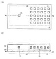
- FIG. 4A is a top view of the semiconductor device.
- 4B is a cross-sectional view taken along dashed-dotted line A1-A2 in FIG. In FIG. 4, some elements are omitted for clarity of illustration.
- the substrate 10 has a region 12 and a region 11.
- the region 12 has elements 16 arranged at a low density and a plurality of dummy elements 18.
- a plurality of structures showing the dummy elements 18 are hatched.
- the region 11 has a plurality of elements 16 arranged at high density.
- a structure 13 including an oxide containing oxygen in excess of the stoichiometric composition is disposed over the region 11 and the region 12.
- the dummy element 18 by disposing the dummy element 18, impurities (typically hydrogen, water, and the like) in the oxide semiconductor are absorbed by the conductor included in the dummy element 18 due to thermal history in the process of forming the transistor. There is a case. That is, the dummy element 18 can suppress the diffusion of the impurity into the element 16 by capturing the impurity. Therefore, the reliability of the element 16 can be improved.
- impurities typically hydrogen, water, and the like
- FIG. 6A is a top view of the semiconductor device.
- 6B and 6C are cross-sectional views of a portion indicated by dashed-dotted line A1-A2 in FIG. In FIG. 6, some elements are omitted for clarity of illustration.
- the substrate 10 has a region 12 and a region 11.
- the region 12 has elements 16 arranged at a low density and a plurality of dummy elements 18.
- a plurality of structures showing the dummy elements 18 are hatched.
- the region 11 has a plurality of elements 16 arranged at high density.
- FIG. 6B a film 15 serving as a structure constituting the element 16 and the dummy element 18 is formed over the substrate 10, and the film 15 is processed by a dry etching method using the mask 17.
- the process is shown schematically.
- FIG. 6C schematically shows the moment when the film 15 is divided by the processing. It is assumed that a plurality of elements 16 and a plurality of dummy elements 18 are formed by dividing the film 15.
- ions accelerated by the plasma 19 selectively remove a part of the film 15 by sputter removing the surface of the film 15.
- the film 15 is divided, and a plurality of elements 16 and a plurality of dummy elements 18 are formed.
- the region 12 and the region 11 are the elements 16 per one.
- the plasma charge amount is equal. That is, plasma charge is induced not only in the element 16 but also in the dummy element 18 in the region 12, so that the plasma charge amount of the element 16 per one is reduced. Accordingly, plasma damage of the element 16 in the region 12 can be reduced and electrostatic breakdown can be suppressed.
- FIG. 8B is a cross-sectional view taken along dashed-dotted line A1-A2 in FIG.
- FIG. 8B schematically illustrates a process in which a film 15 which is a structure constituting the element 16 is formed over the substrate 10 and the film 15 is processed by a dry etching method using the mask 17. Is shown.
- the arrow in a figure shows the accelerated ion.
- region 11 and region 12 a thin film accompanied by a deposition reaction is processed, so that a deposited film 14 is formed.
- processing is performed at an equivalent processing speed, so that the shape of the element In addition, variations in characteristics can be suppressed.
- FIGS. 1 to 3 show a part of a region corresponding to the region 12 shown in FIG. Therefore, the semiconductor device has a region 11 in which elements are arranged at a high density in addition to the region 12 shown in FIGS.
- the region 12 includes a dummy transistor in addition to a transistor functioning as a transistor, and thus has an element pattern density equivalent to that of the region 11.
- the element density is equivalent to the region 11 in which the elements are arranged at high density.
- a transistor functioning as a transistor and a transistor functioning as a sacrificial element (hereinafter also referred to as a dummy transistor) are arranged.
- FIG. 1D is an example of a schematic diagram of a transistor 200 according to one embodiment of the present invention. Note that in FIG. 1D, some elements are omitted for clarity of illustration.
- the transistor 200 includes at least a conductor 260 functioning as a first gate, an oxide 230 having a region where a channel is formed (hereinafter also referred to as a channel formation region), It has a conductor 240s functioning as a source and a conductor 240d functioning as a drain.
- the transistor 200 may include a conductor 205 functioning as a second gate below the oxide 230.
- the threshold voltage of the transistor 200 can be controlled by changing the potential applied to the conductor 205 independently of the potential applied to the conductor 260 without being linked.
- the threshold voltage of the transistor 200 can be made higher than 0 V and the off-state current can be reduced. Therefore, when a negative potential is applied to the conductor 205, the drain current when the potential applied to the conductor 260 is 0 V can be made smaller than when a negative potential is not applied.
- the conductor 205 and the conductor 260 so as to overlap with each other, when the same potential is applied to the conductor 260 and the conductor 205, the electric field generated from the conductor 260 and the conductor 205 are generated.
- the channel formation region formed in the oxide 230 can be covered with an electric field.
- the channel formation region can be electrically surrounded by the electric field of the conductor 260 functioning as the first gate electrode and the electric field of the conductor 205 functioning as the second gate electrode.
- a transistor structure that electrically surrounds a channel formation region by an electric field of the first gate electrode and the second gate electrode is referred to as a surrounded channel (S-channel) structure.
- a metal oxide containing indium is preferably used as the oxide 230.
- an In-M-Zn oxide (the element M1 is aluminum, gallium, yttrium, copper, vanadium, beryllium, boron, titanium, iron, nickel, germanium, zirconium, molybdenum, lanthanum, hafnium, tantalum, tungsten, or magnesium.
- a metal oxide such as one or more selected from the above can be used.
- an In—Ga oxide or an In—Zn oxide may be used as the oxide 230.
- the transistor 200 using an oxide semiconductor in a region where a channel is formed has extremely small leakage current in a non-conduction state, a low power consumption semiconductor device can be provided.
- the transistor 200 can be stacked and integrated three-dimensionally by using an oxide semiconductor as an active layer.
- n and m are natural numbers
- arbitrary transistors 200 are assigned coordinates, and the transistor 200 (I, j).
- the region 12 only needs to have an element pattern density equivalent to at least the region where the elements are arranged at a higher density than the region 12 (the region 11 shown in FIGS. 4 and 6). Accordingly, FIGS. 1 to 3 show an example in which they are arranged in a matrix for convenience of explanation, but the layout including dummy elements is not limited to a matrix. What is necessary is just to design suitably according to the circuit to request
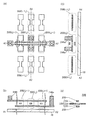
- FIG. 1A illustrates a transistor located in the i-th row and j-th column among n ⁇ m transistors or dummy transistors arranged in a matrix in the region 12 of the semiconductor device according to one embodiment of the present invention.
- FIG. 11 is a top view of a region including a transistor 200 (i, j + 1).
- dummy transistors are arranged on the four sides of the transistor 200 (i, j) for the sake of simplicity of explanation, but the present invention is not limited to this structure. At least one of the elements adjacent to the transistor 200 (i, j) may be a dummy transistor.
- FIG. 1B is a cross-sectional view of a portion indicated by alternate long and short dash line A1-A2 in FIG.
- FIG. 1C is a cross-sectional view taken along dashed-dotted line A3-A4 in FIG. In FIG. 1, some elements are omitted for clarity of illustration.
- the transistor 200 (i, j), the dummy transistor 200 (i-1, j), the dummy transistor 200 (i + 1, j), the dummy transistor 200 (i, j-1), and the dummy transistor 200 (i, j + 1) ) Is formed in the same step, and thus is disposed in the same layer. Accordingly, the dummy transistor 200 (i ⁇ 1, j), the dummy transistor 200 (i + 1, j), the dummy transistor 200 (i, j ⁇ 1), and the dummy transistor 200 (i, j + 1) are the same as the transistor 200 (i, j). And a transistor having the same structure may be used as a dummy transistor.
- the transistor 200 includes at least a conductor 260 functioning as a first gate and a region where a channel is formed (hereinafter also referred to as a channel formation region). And the conductor 240s functioning as a source and the conductor 240d functioning as a drain.
- the dummy transistor 200 (i ⁇ 1, j), the dummy transistor 200 (i + 1, j), the dummy transistor 200 (i, j ⁇ 1), and the dummy transistor 200 (i, j + 1) are not necessarily limited to the transistor 200 (i , J) need not have the same structure.
- the dummy transistor 200 (i ⁇ 1, j), the dummy transistor 200 (i + 1, j), the dummy transistor 200 (i, j ⁇ 1), and the dummy transistor 200 (i, j + 1) include a structure made of a conductor, and At least one of the structures made of a semiconductor is included.
- the conductor included in the dummy transistor is a conductor formed in the same step as the conductor included in the transistor 200 (i, j).
- the semiconductor included in the dummy transistor is a semiconductor formed in the same step as the conductor included in the transistor 200 (i, j).
- the dummy transistor 200 (i ⁇ 1, j), the dummy transistor 200 (i + 1, j), the dummy transistor 200 (i, j ⁇ 1), and the dummy transistor 200 (i, j + 1) , Oxide 230, conductor 240s, and conductor 240d.
- the dummy transistor 200 (i, j ⁇ 1) and the dummy transistor 200 (i, j + 1) further include a conductor 260 and a conductor 205.
- the conductor 260 and the conductor 205 included in the dummy transistor 200 (i, j ⁇ 1) and the dummy transistor 200 (i, j + 1) are electrically connected to the conductor 260 and the conductor 205 of the transistor 200 (i, j). It may have a function as a wiring by connecting them electrically.
- the conductor 260 and the conductor 205 can be electrically connected to an external terminal through the plug 246t and the plug 246b.
- the conductor 240s and the conductor 240d are electrically connected to the plug 246s and the plug 246d.
- the conductor 240s and the conductor 240d of the dummy transistor are in a floating state, but the plug 246s and the plug 246d connected to the transistor 200 (i, j) and the plug are provided in the same process, so that the external You may electrically connect with a terminal.
- the semiconductor device illustrated in FIG. 1 includes a dummy transistor 200 (i ⁇ 1, j), a dummy transistor 200 (i + 1, j), a dummy transistor 200 (i, j ⁇ 1), and a dummy transistor 200 (i, j + 1).
- a dummy transistor 200 i ⁇ 1, j
- a dummy transistor 200 i + 1, j
- a dummy transistor 200 i, j ⁇ 1
- a dummy transistor 200 i, j + 1
- the dummy transistor 200 (i ⁇ 1, j) and the dummy transistor are formed when the oxide 230 of the transistor 200 (i, j) or the conductor 240 s and the conductor 240 d are formed.
- 200 (i + 1, j), dummy transistor 200 (i, j-1), and dummy transistor 200 (i, j + 1) oxide 230, conductor 240s, and conductor 240d are formed simultaneously, thereby forming a shape by processing. Abnormalities can be suppressed.
- by suppressing the oxide 230 of the transistor 200 (i, j) from being charged up electrostatic breakdown of the insulator disposed between the oxide 230 and the conductor 205 can be prevented.
- the conductor 260 may be provided in the dummy transistor 200 (i + 1, j) and the dummy transistor 200 (i-1, j). With this structure, the amount of excess oxygen diffused from the oxide having excess oxygen arranged in the vicinity of the transistor 200 (i, j) to the transistor 200 (i, j) can be controlled.
- the dummy transistor 200 (i + 1, j) and the dummy transistor 200 (i-1, j) are provided with the conductor 260, whereby the transistor The charge-up of the 200 (i, j) conductor 260 can be suppressed. Therefore, electrostatic breakdown of the insulator disposed between the conductor 260 and the oxide 230 can be prevented.
- FIG. 2A is a top view of a region 12 included in a semiconductor device including an element including an oxide semiconductor which is one embodiment of the present invention.
- FIG. 2B is a cross-sectional view taken along dashed-dotted line A1-A2 in FIG.
- FIG. 2C is a cross-sectional view taken along dashed-dotted line A3-A4 in FIG.
- some elements are omitted for clarity of illustration.
- the semiconductor device illustrated in FIG. 2 is different from the semiconductor device illustrated in FIG. 1 in that the dummy transistor 200 (i ⁇ 1, j), the dummy transistor 200 (i + 1, j), the dummy transistor 200 (i, j ⁇ 1), and the dummy
- the shapes of the conductors 240s and 240d of the transistor 200 (i, j + 1) are different.
- the dummy transistor 200 (i-1, j) the dummy transistor 200 (i + 1, j), the dummy transistor 200 (i, j-1), and the dummy transistor 200 (i, j + 1)
- the body 240s and the conductor 240d do not need to be divided.
- the conductors 240s and 240d of the dummy transistor may overlap with a region corresponding to the channel formation region.
- the structure of the dummy transistor and the structure of the transistor 200 (i, j) may be made common.
- the conductor 240s of the transistor 200 (i, j) overlaps with the oxide 230 of the dummy transistor 200 (i + 1, j). Also good.
- the conductor 240d of the transistor 200 (i, j) may overlap with the oxide 230 of the dummy transistor 200 (i-1, j).
- the conductor 240s and the conductor 240d can be formed sufficiently wide. Therefore, the amount of excess oxygen diffused can be adjusted as appropriate.
- the conductor 240s and the conductor 240d can be formed sufficiently wide, so that charge-up during the manufacturing process can be reduced.
- the conductor 240s and the conductor 240d are sufficiently larger than the transistor 200 (i, j), and thus potential fluctuation is less likely to occur due to charges absorbed by the conductor 240s and the conductor 240d.
- the conductor 240s and the conductor 240d can be used as wiring.
- FIG. 3A is a top view of a region 12 included in a semiconductor device including an element including an oxide semiconductor which is one embodiment of the present invention.
- FIG. 3B is a cross-sectional view taken along dashed-dotted line A1-A2 in FIG.
- FIG. 3C is a cross-sectional view taken along dashed-dotted line A3-A4 in FIG.
- some elements are omitted for clarity of illustration.
- the addition of an element that forms oxygen vacancies or an element that combines with oxygen vacancies may increase carrier density and reduce resistance.
- the source region or the drain region can be provided by selectively reducing the resistance of the oxide 230.
- an element that lowers the resistance of an oxide semiconductor typically, boron or phosphorus can be given.
- hydrogen, carbon, nitrogen, fluorine, sulfur, chlorine, titanium, rare gas, or the like may be used.
- the rare gas include helium, neon, argon, krypton, and xenon.
- an ion implantation method in which an ionized source gas is added by mass separation an ion doping method in which an ionized source gas is added without mass separation, a plasma immersion ion implantation method, or the like can be used.
- the dummy transistors 200 (i ⁇ 1, j), the dummy transistors 200 (i + 1, j), the dummy transistors 200 (i, j ⁇ 1), and the dummy transistors 200 (i, j + 1) Unlike the transistor 200 (i, j), the entire surface of the oxide 230 may have a low resistance.
- the oxide 230 with a reduced resistance of the dummy transistor is extended so that the source region or the drain region of the oxide 230 in the transistor 200 (i, j) is integrated. May be.
- the conductor 240s and the conductor 240d can be formed sufficiently wide. Therefore, the amount of excess oxygen diffused can be adjusted as appropriate. Further, with this structure, the source region and the drain region of the transistor 200 (i, j) can be formed sufficiently wide, so that charge-up during the manufacturing process can be reduced.
- the source region and the drain region of the transistor 200 can be used as wirings.
- a highly integrated semiconductor device can be easily used.
- a semiconductor device including a transistor with high on-state current can be provided.
- a semiconductor device including a transistor with low off-state current can be provided.
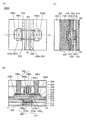
- FIG. 9A is a top view of the transistor 200A.
- FIG. 9B is a cross-sectional view taken along dashed-dotted line L1-L2 in FIG.
- FIG. 9C is a cross-sectional view taken along dashed-dotted line W1-W2 in FIG. Note that in the top view of FIG. 9A, some elements are omitted for clarity.
- the transistor 200A the insulator 210 functioning as an interlayer film, the insulator 212, the insulator 214, the insulator 216, the insulator 280, the insulator 282, and the insulator 284; Is shown.
- a plug 246 (a plug 246s and a plug 246d) that is electrically connected to the transistor 200A and functions as a contact plug, and a conductor 203 that functions as a wiring are illustrated.
- the transistor 200A includes a conductor 260 (also referred to as a conductor 260a and a conductor 260b) that functions as a first gate (also referred to as a top gate) electrode and a conductor that functions as a second gate (also referred to as a bottom gate) electrode.
- a conductor 260 also referred to as a conductor 260a and a conductor 260b
- first gate also referred to as a top gate
- a second gate also referred to as a bottom gate
- Body 205 (conductor 205a and conductor 205b), insulator 250 functioning as a first gate insulator, insulator 220, insulator 222, and insulator 224 functioning as a second gate insulator ,
- An oxide 230 having a region where a channel is formed (oxide 230a, oxide 230b, and oxide 230c), a conductor 240s functioning as one of a source or a drain, and a conductivity functioning as the other of a source or a drain
- the insulator 210 and the insulator 212 function as an interlayer film.
- An insulator such as TiO 3 (BST) can be used in a single layer or a stacked layer.
- aluminum oxide, bismuth oxide, germanium oxide, niobium oxide, silicon oxide, titanium oxide, tungsten oxide, yttrium oxide, or zirconium oxide may be added to these insulators.
- these insulators may be nitrided. Silicon insulator, silicon oxynitride, or silicon nitride may be stacked over the above insulator.
- the insulator 210 preferably functions as a barrier film that suppresses impurities such as water and hydrogen from entering the transistor 200A from the substrate side. Therefore, the insulator 210 is preferably formed using an insulating material having a function of suppressing the diffusion of impurities such as hydrogen atoms, hydrogen molecules, water molecules, and copper atoms (the impurities are difficult to transmit). Alternatively, it is preferable to use an insulating material having a function of suppressing diffusion of oxygen (for example, at least one of an oxygen atom and an oxygen molecule) (the oxygen hardly transmits). For example, as the insulator 210, aluminum oxide, silicon nitride, or the like may be used. With this structure, impurities such as water and hydrogen can be prevented from diffusing from the substrate side to the transistor 200A side with respect to the insulator 210.
- the insulator 212 preferably has a lower dielectric constant than the insulator 210.
- parasitic capacitance generated between the wirings can be reduced.
- the conductor 203 is formed so as to be embedded in the insulator 212.
- the height of the upper surface of the conductor 203 and the height of the upper surface of the insulator 212 can be approximately the same.
- the conductor 203 has a single-layer structure, the present invention is not limited to this.
- the conductor 203 may have a multilayer film structure of two or more layers.
- the conductor 203 is preferably formed using a conductive material having tungsten, copper, or aluminum as its main component and having relatively high conductivity.
- the conductor 260 may function as a first gate electrode.
- the conductor 205 may function as a second gate electrode.
- the threshold voltage of the transistor 200 ⁇ / b> A can be controlled by changing the potential applied to the conductor 205 independently of the potential applied to the conductor 260 without being interlocked with the potential applied to the conductor 260.
- the threshold voltage of the transistor 200A can be higher than 0 V and the off-state current can be reduced. Therefore, when a negative potential is applied to the conductor 205, the drain current when the potential applied to the conductor 260 is 0 V can be made smaller than when a negative potential is not applied.
- the conductor 205 and the conductor 260 are provided so as to overlap with each other, when an electric potential is applied to the conductor 260 and the conductor 205, an electric field generated from the conductor 260 and an electric field generated from the conductor 205 , And a channel formation region formed in the oxide 230 can be covered.
- the channel formation region can be electrically surrounded by the electric field of the conductor 260 functioning as the first gate electrode and the electric field of the conductor 205 functioning as the second gate electrode.
- a transistor structure that electrically surrounds a channel formation region by an electric field of the first gate electrode and the second gate electrode is referred to as a surrounded channel (S-channel) structure.
- the insulator 214 and the insulator 216 function as an interlayer film like the insulator 210 or the insulator 212.
- the insulator 214 preferably functions as a barrier film that suppresses impurities such as water and hydrogen from entering the transistor 200A from the substrate side. With this structure, impurities such as water and hydrogen can be prevented from diffusing from the substrate side to the transistor 200A side with respect to the insulator 214.
- the insulator 216 preferably has a lower dielectric constant than the insulator 214. By using a material having a low dielectric constant as the interlayer film, parasitic capacitance generated between the wirings can be reduced.
- a conductor 205a is formed in contact with the inner walls of the openings of the insulator 214 and the insulator 216, and a conductor 205b is further formed inside.
- the heights of the upper surfaces of the conductors 205a and 205b and the height of the upper surface of the insulator 216 can be approximately the same.
- the transistor 200A shows a structure in which the conductors 205a and 205b are stacked, the present invention is not limited to this.
- the conductor 205 may be provided as a single layer or a stacked structure including three or more layers.
- the conductor 205a be made of a conductive material having a function of suppressing diffusion of impurities such as hydrogen atoms, hydrogen molecules, water molecules, and copper atoms (the impurities are difficult to permeate).
- impurities such as hydrogen atoms, hydrogen molecules, water molecules, and copper atoms
- a conductive material having a function of suppressing diffusion of oxygen for example, at least one of oxygen atoms and oxygen molecules
- the oxygen hardly transmits.
- the function of suppressing diffusion of impurities or oxygen is a function of suppressing diffusion of any one or all of the impurities or oxygen.
- the conductor 205a has a function of suppressing the diffusion of oxygen, it is possible to suppress the conductivity of the conductor 205b from being reduced due to oxidation.
- the conductor 205b is preferably formed using a highly conductive material containing tungsten, copper, or aluminum as a main component. In that case, the conductor 203 is not necessarily provided. Note that although the conductor 205b is illustrated as a single layer, it may have a stacked structure, for example, a stack of titanium, titanium nitride, and the above-described conductive material.
- the insulator 220, the insulator 222, and the insulator 224 function as a second gate insulator.
- the insulator 224 in contact with the oxide 230 desorbs oxygen by heating.
- oxygen that is desorbed by heating may be referred to as excess oxygen.
- the insulator 224 may be formed using silicon oxide, silicon oxynitride, or the like as appropriate.
- an oxide material from which part of oxygen is released by heating is preferably used as the insulator 224.
- the oxide that desorbs oxygen by heating means that the amount of desorbed oxygen in terms of oxygen atom is 1.0 ⁇ 10 18 atoms / cm 3 or more, preferably 1 in TDS (Thermal Desorption Spectroscopy) analysis.
- the oxide is 0.0 ⁇ 10 19 atoms / cm 3 or more, more preferably 2.0 ⁇ 10 19 atoms / cm 3 or more, or 3.0 ⁇ 10 20 atoms / cm 3 or more.
- the surface temperature of the film at the time of the TDS analysis is preferably in the range of 100 ° C. to 700 ° C.
- the insulator 222 preferably has a barrier property.
- the insulator 222 functions as a layer that suppresses entry of impurities such as hydrogen from the peripheral portion of the transistor 200A to the transistor 200A.
- the insulator 222 includes, for example, aluminum oxide, hafnium oxide, aluminum and an oxide containing hafnium (hafnium aluminate), tantalum oxide, zirconium oxide, lead zirconate titanate (PZT), strontium titanate (SrTiO 3 ), (
- An insulator including a so-called high-k material such as Ba, Sr) TiO 3 (BST) is preferably used in a single layer or a stacked layer.
- problems such as leakage current may occur due to thinning of the gate insulator.
- a high-k material for the insulator functioning as a gate insulator the gate potential during transistor operation can be reduced while maintaining the physical film thickness.
- the insulator 220 is thermally stable.
- silicon oxide and silicon oxynitride are thermally stable, by combining with an insulator 222 using an insulator of a high-k material, a stacked structure having a high thermal stability and a high relative dielectric constant can be obtained. can do.
- FIG. 9 illustrates a three-layer stacked structure as the second gate insulator, a single-layered, two-layered, or four-layered stacked structure may be used. In that case, the present invention is not limited to a laminated structure made of the same material, and may be a laminated structure made of different materials.
- the oxide 230 having a region functioning as a channel formation region includes the oxide 230a, the oxide 230b over the oxide 230a, and the oxide 230c over the oxide 230b.
- the oxide 230a under the oxide 230b diffusion of impurities from the structure formed below the oxide 230a to the oxide 230b can be suppressed.
- the oxide 230c over the oxide 230b diffusion of impurities from the structure formed above the oxide 230c to the oxide 230b can be suppressed.
- the oxide 230 an oxide semiconductor which is a kind of metal oxide described below can be used.
- the transistor 200A illustrated in FIG. 9 includes a region where the conductor 240 (the conductor 240s and the conductor 240d) overlaps with the oxide 230c, the insulator 250, and the conductor 260.
- a transistor with high on-state current can be provided.
- a transistor with high controllability can be provided.
- One of the conductors 240 functions as a source electrode, and the other functions as a drain electrode.
- a metal such as aluminum, titanium, chromium, nickel, copper, yttrium, zirconium, molybdenum, silver, tantalum, or tungsten, or an alloy containing the metal as a main component can be used.
- a metal nitride film such as tantalum nitride is preferable because it has a barrier property against hydrogen or oxygen and has high oxidation resistance.
- the conductor 240 may have a laminated structure of two or more layers.
- a tantalum nitride film and a tungsten film are preferably stacked.
- a titanium film and an aluminum film may be stacked.
- a two-layer structure in which an aluminum film is stacked on a tungsten film a two-layer structure in which a copper film is stacked on a copper-magnesium-aluminum alloy film, a two-layer structure in which a copper film is stacked on a titanium film, and a tungsten film
- a two-layer structure in which copper films are stacked may be used.
- a transparent conductive material containing indium oxide, tin oxide, or zinc oxide may be used.
- a barrier layer may be provided on the conductor 240.
- the barrier layer is preferably formed using a substance having a barrier property against oxygen or hydrogen. With this structure, oxidation of the conductor 240 can be suppressed when the insulator 274 is formed.
- a metal oxide for example, a metal oxide can be used.
- an insulating film having a barrier property against oxygen and hydrogen such as aluminum oxide, hafnium oxide, and gallium oxide, is preferably used.
- silicon nitride formed by a CVD method may be used.
- the material selection range of the conductor 240 can be expanded.
- a material having high conductivity while having low oxidation resistance such as tungsten or aluminum, can be used for the conductor 240.
- a conductor that can be easily formed or processed can be used.
- the insulator 250 functions as a first gate insulator.
- the insulator 250 may have a stacked structure similar to the second gate insulator.
- the insulator that functions as a gate insulator has a stacked structure of a high-k material and a thermally stable material, so that the gate potential during transistor operation can be reduced while maintaining the physical film thickness. It becomes.
- the conductor 260 functioning as the first gate electrode includes a conductor 260a and a conductor 260b over the conductor 260a.
- the conductor 260a is preferably formed using a conductive material having a function of suppressing diffusion of impurities such as a hydrogen atom, a hydrogen molecule, a water molecule, and a copper atom, like the conductor 205a.
- a conductive material having a function of suppressing diffusion of oxygen for example, at least one of oxygen atoms and oxygen molecules).
- the conductor 260a has a function of suppressing the diffusion of oxygen, the material selectivity of the conductor 260b can be improved. That is, by including the conductor 260a, oxidation of the conductor 260b can be suppressed and the conductivity can be prevented from decreasing.
- tantalum, tantalum nitride, ruthenium, ruthenium oxide, or the like is preferably used as the conductive material having a function of suppressing oxygen diffusion.
- the conductor 260a an oxide semiconductor that can be used as the oxide 230 can be used. In that case, by forming the conductor 260b by a sputtering method, the electrical resistance value of the oxide semiconductor to be the conductor 260a can be reduced, whereby the conductor can be obtained. This can be called an OC (Oxide Conductor) electrode.
- the conductor 260 functions as a wiring, it is preferable to use a conductor having high conductivity.
- the conductor 260b can be formed using a conductive material containing tungsten, copper, or aluminum as a main component.
- the conductor 260b may have a stacked structure, for example, a stack of titanium, titanium nitride, and the above conductive material.
- the insulator 274 is preferably provided so as to cover the top surface and the side surface of the conductor 260, the side surface of the insulator 250, and the side surface of the oxide 230c.
- the insulator 274 may be formed using an insulating material having a function of suppressing diffusion of impurities such as water and hydrogen, and oxygen.
- aluminum oxide or hafnium oxide is preferably used.
- metal oxides such as magnesium oxide, gallium oxide, germanium oxide, yttrium oxide, zirconium oxide, lanthanum oxide, neodymium oxide, and tantalum oxide, silicon nitride oxide, silicon nitride, and the like can be used.
- oxidation of the conductor 260 can be suppressed.
- impurities such as water and hydrogen included in the insulator 280 can be prevented from diffusing into the transistor 200A.
- the insulator 280, the insulator 282, and the insulator 284 function as an interlayer film.
- the insulator 282 preferably functions as a barrier insulating film that suppresses impurities such as water and hydrogen from entering the transistor 200A from the outside.
- the insulator 280 and the insulator 284 preferably have a dielectric constant lower than that of the insulator 282.
- parasitic capacitance generated between the wirings can be reduced.
- the transistor 200A may be electrically connected to another structure through a plug or a wiring such as the insulator 280, the insulator 282, and the plug 246 embedded in the insulator 284.
- a conductive material such as a metal material, an alloy material, a metal nitride material, or a metal oxide material can be used as a single layer or a stacked layer.
- a high melting point material such as tungsten or molybdenum that has both heat resistance and conductivity.
- a low-resistance conductive material such as aluminum or copper. Wiring resistance can be lowered by using a low-resistance conductive material.
- the plug 246 for example, by using a stacked structure of tantalum nitride which is a conductor having a barrier property against hydrogen and oxygen and tungsten having high conductivity, conductivity as a wiring is maintained. Thus, diffusion of impurities from the outside can be suppressed.
- an insulator 276 having a barrier property may be disposed between the plug 246 and the insulator 280.
- the plug 246 can be provided with a semiconductor device with low power consumption by using a metal material that absorbs oxygen but has high conductivity.
- a material having low conductivity but high conductivity such as tungsten or aluminum can be used.
- a conductor that can be easily formed or processed can be used.
- a semiconductor device including a transistor with high on-state current can be provided.
- a semiconductor device including a transistor with low off-state current can be provided.
- the material used for the substrate it is necessary that the substrate have heat resistance enough to withstand at least heat treatment performed later.
- a single crystal semiconductor substrate using a material such as silicon or silicon carbide, a polycrystalline semiconductor substrate, a compound semiconductor substrate using silicon germanium, or the like as the substrate can be used.
- an SOI substrate or a semiconductor substrate provided with a semiconductor element such as a strain transistor or a FIN transistor can be used.
- gallium arsenide, aluminum gallium arsenide, indium gallium arsenide, gallium nitride, indium phosphide, silicon germanium, or the like that can be used for a high electron mobility transistor (HEMT) may be used. That is, the substrate is not limited to a simple support substrate, and may be a substrate on which other devices such as transistors are formed.
- a glass substrate such as barium borosilicate glass or alumino borosilicate glass, a ceramic substrate, a quartz substrate, a sapphire substrate, or the like can be used as the substrate.
- a flexible substrate flexible substrate
- a transistor, a capacitor, or the like may be directly formed over the flexible substrate, or a transistor, a capacitor, or the like is formed over another manufacturing substrate, and then the flexible substrate is formed. You may peel and transpose.
- a separation layer may be provided between the manufacturing substrate and a transistor, a capacitor, or the like in order to separate and transfer from the manufacturing substrate to the flexible substrate.
- the flexible substrate for example, metal, alloy, resin or glass, or fiber thereof can be used.
- the flexible substrate used for the substrate is preferably as the linear expansion coefficient is low because deformation due to the environment is suppressed.
- a material having a linear expansion coefficient of 1 ⁇ 10 ⁇ 3 / K or less, 5 ⁇ 10 ⁇ 5 / K or less, or 1 ⁇ 10 ⁇ 5 / K or less may be used.
- the resin include polyester, polyolefin, polyamide (such as nylon and aramid), polyimide, polycarbonate, and acrylic.
- aramid has a low coefficient of linear expansion, it is suitable as a flexible substrate.
- the insulator is aluminum nitride, aluminum oxide, aluminum nitride oxide, aluminum oxynitride, magnesium oxide, silicon nitride, silicon oxide, silicon nitride oxide, silicon oxynitride, gallium oxide, germanium oxide, yttrium oxide, zirconium oxide, lanthanum oxide,
- a material selected from neodymium oxide, hafnium oxide, tantalum oxide, aluminum silicate, or the like is used as a single layer or a stacked layer.
- a material obtained by mixing a plurality of materials among oxide materials, nitride materials, oxynitride materials, and nitride oxide materials may be used.
- a nitrided oxide refers to a compound having a higher nitrogen content than oxygen.
- oxynitride refers to a compound having a higher oxygen content than nitrogen.
- content of each element can be measured using Rutherford backscattering method (RBS: Rutherford Backscattering Spectrometry) etc., for example.
- the hydrogen concentration in the insulator is set to 2 ⁇ 10 20 atoms / cm 3 or less, preferably 5 ⁇ 10 19 atoms / cm 3 or less in Secondary Ion Mass Spectrometry (SIMS). More preferably, it is 1 ⁇ 10 19 atoms / cm 3 or less, and further preferably 5 ⁇ 10 18 atoms / cm 3 or less. In particular, it is preferable to reduce the hydrogen concentration of the insulator in contact with the semiconductor layer.
- SIMS Secondary Ion Mass Spectrometry
- the nitrogen concentration in the insulator is 5 ⁇ 10 19 atoms / cm 3 or less, preferably 5 ⁇ 10 18 atoms / cm 3 or less, more preferably 1 ⁇ 10 18 atoms / cm 3 or less in SIMS, More preferably, it is 5 ⁇ 10 17 atoms / cm 3 or less.
- the signal described above includes the E ′ center where the g value is observed at 2.001.
- the E ′ center is caused by silicon dangling bonds.
- the spin density due to the E ′ center is 3 ⁇ 10 17 spins / cm 3 or less, preferably 5 ⁇ 10 16 spins / cm 3 or less.
- a silicon oxide layer or a silicon oxynitride layer may be used.
- a signal due to nitrogen dioxide (NO 2 ) may be observed.
- the signal is split into three signals by the nuclear spin of nitrogen, each having a g value of 2.037 to 2.039 (referred to as the first signal), and a g value of 2.001 to 2.003.
- the g value is observed below (referred to as a second signal), and the g value is observed from 1.964 to 1.966 (referred to as a third signal).
- NO 2 nitrogen dioxide
- nitrogen oxide (NO x ) containing nitrogen dioxide (NO 2 ) forms a level in the insulator.
- the level is located in the energy gap of the oxide semiconductor layer. Therefore, when nitrogen oxide (NO x ) diffuses to the interface between the insulator and the oxide semiconductor layer, the level may trap electrons on the insulator side. As a result, trapped electrons remain in the vicinity of the interface between the insulator and the oxide semiconductor layer, so that the threshold voltage of the transistor is shifted in the positive direction. Therefore, when a film with a low content of nitrogen oxide is used as the insulator, a shift in threshold voltage of the transistor can be reduced.
- a silicon oxynitride layer can be used as the insulator that releases less nitrogen oxide (NO x ).
- the silicon oxynitride layer is a film in which the amount of ammonia released is larger than the amount of nitrogen oxide (NO x ) released in a temperature programmed desorption gas analysis (TDS: Thermal Desorption Spectroscopy).
- TDS Thermal Desorption Spectroscopy
- the discharge amount is 1 ⁇ 10 18 pieces / cm 3 or more and 5 ⁇ 10 19 pieces / cm 3 or less.
- the amount of ammonia released is the total amount when the temperature of the heat treatment in TDS is 50 ° C. or higher and 650 ° C. or lower, or 50 ° C. or higher and 550 ° C. or lower.
- nitrogen oxide (NO x ) reacts with ammonia and oxygen in heat treatment, nitrogen oxide (NO x ) is reduced by using an insulator that releases a large amount of ammonia.
- At least one of the insulators in contact with the oxide semiconductor layer is preferably formed using an insulator from which oxygen is released by heating.
- the amount of desorbed oxygen converted to oxygen atoms is 1.0 in TDS performed by heat treatment at a surface temperature of the insulator of 100 ° C. to 700 ° C., preferably 100 ° C. to 500 ° C.
- An insulator having ⁇ 10 18 atoms / cm 3 or more, 1.0 ⁇ 10 19 atoms / cm 3 or more, or 1.0 ⁇ 10 20 atoms / cm 3 or more is preferably used. Note that in this specification and the like, oxygen released by heating is also referred to as “excess oxygen”.
- An insulator containing excess oxygen can also be formed by performing treatment for adding oxygen to the insulator.
- the treatment for adding oxygen can be performed by heat treatment or plasma treatment in an oxidizing atmosphere.
- oxygen may be added by an ion implantation method, an ion doping method, a plasma immersion ion implantation method, or the like.
- a gas used for the process of adding oxygen an oxygen gas such as 16 O 2 or 18 O 2 , a gas containing oxygen such as a nitrous oxide gas, and an ozone gas can be given.
- oxygen doping treatment may be performed by heating the substrate.
- a heat-resistant organic material such as polyimide, acrylic resin, benzocyclobutene resin, polyamide, or epoxy resin can be used.
- a low dielectric constant material low-k material
- a siloxane resin PSG (phosphorus glass), BPSG (phosphorus boron glass), or the like can be used.
- the insulator may be formed by stacking a plurality of insulators formed using these materials.
- siloxane-based resin corresponds to a resin including a Si—O—Si bond formed using a siloxane-based material as a starting material.
- Siloxane resins may use organic groups (for example, alkyl groups and aryl groups) and fluoro groups as substituents.
- the organic group may have a fluoro group.
- the method for forming the insulator is not particularly limited. Note that depending on the material used for the insulator, a baking step may be required. In this case, the transistor can be efficiently manufactured by combining the baking process of the insulator and the other heat treatment process.
- Electrodes examples include aluminum, chromium, copper, silver, gold, platinum, tantalum, nickel, titanium, molybdenum, tungsten, hafnium, vanadium, niobium, manganese, magnesium, zirconium, beryllium, indium, etc.
- a material containing one or more metal elements selected from the above can be used.
- a semiconductor with high electrical conductivity typified by polycrystalline silicon containing an impurity element such as phosphorus, or silicide such as nickel silicide may be used.
- a conductive material containing the above metal element and oxygen may be used.
- a conductive material containing the above metal element and nitrogen may be used.
- a conductive material containing nitrogen such as titanium nitride or tantalum nitride may be used.
- Indium tin oxide ITO: Indium Tin Oxide
- indium oxide containing tungsten oxide indium zinc oxide containing tungsten oxide
- indium oxide containing titanium oxide indium tin oxide containing titanium oxide
- indium tin oxide containing titanium oxide indium zinc An oxide
- indium gallium zinc oxide, or indium tin oxide to which silicon is added may be used.
- indium gallium zinc oxide containing nitrogen may be used.
- a plurality of conductors formed of the above materials may be used.
- a stacked structure in which the above-described material containing a metal element and a conductive material containing oxygen may be combined.
- a stacked structure in which the above-described material containing a metal element and a conductive material containing nitrogen are combined may be employed.
- a stacked structure of a combination of the above-described material containing a metal element, a conductive material containing oxygen, and a conductive material containing nitrogen may be employed.
- a stacked structure of a conductive material containing nitrogen and a conductive material containing oxygen may be used.
- the conductive material containing oxygen is used as a semiconductor. It is good to provide on the layer side. By providing a conductive material containing oxygen on the semiconductor layer side, oxygen released from the conductive material can be easily supplied to the semiconductor layer.
- a highly embedded conductive material such as tungsten or polysilicon may be used.
- a conductive material with high embeddability and a barrier layer (diffusion prevention layer) such as a titanium layer, a titanium nitride layer, or a tantalum nitride layer may be used in combination.
- the electrode may be referred to as a “contact plug”.
- a conductive material that does not easily allow impurities to pass through the electrode in contact with the gate insulator is tantalum nitride.
- the reliability of the transistor can be further increased. That is, the reliability of the storage device can be further improved.
- semiconductor layer a single crystal semiconductor, a polycrystalline semiconductor, a microcrystalline semiconductor, an amorphous semiconductor, or the like can be used alone or in combination.
- semiconductor material for example, silicon, germanium, or the like can be used.
- a compound semiconductor such as silicon germanium, silicon carbide, gallium arsenide, an oxide semiconductor, or a nitride semiconductor, an organic semiconductor, or the like can be used.
- a low molecular organic material having an aromatic ring, a ⁇ -electron conjugated conductive polymer, or the like can be used.
- a low molecular organic material having an aromatic ring, a ⁇ -electron conjugated conductive polymer, or the like can be used.
- rubrene, tetracene, pentacene, perylene diimide, tetracyanoquinodimethane, polythiophene, polyacetylene, polyparaphenylene vinylene, and the like can be used.
- a semiconductor layer may be stacked.
- semiconductors having different crystal states may be used, or different semiconductor materials may be used.
- the band gap of an oxide semiconductor which is a kind of metal oxide is 2 eV or more
- the off-current per channel width of 1 ⁇ m is less than 1 ⁇ 10 ⁇ 20 A and 1 ⁇ 10 ⁇ 22 A at a source-drain voltage of 3.5 V and room temperature (typically 25 ° C.). Or less than 1 ⁇ 10 ⁇ 24 A. That is, the on / off ratio can be 20 digits or more.
- a transistor using an oxide semiconductor for a semiconductor layer (OS transistor) has high withstand voltage between a source and a drain.
- a highly reliable transistor can be provided.
- a transistor with a large output voltage and high withstand voltage can be provided.
- a highly reliable storage device or the like can be provided.
- a memory device with a large output voltage and high withstand voltage can be provided.
- a transistor using crystalline silicon for a semiconductor layer in which a channel is formed is also referred to as a “crystalline Si transistor”.
- a crystalline Si transistor is easier to obtain a relatively higher mobility than an OS transistor.
- a crystalline Si transistor is difficult to realize an extremely small off-state current like an OS transistor. Therefore, it is important that the semiconductor material used for the semiconductor layer is properly used depending on the purpose and application.
- an OS transistor and a crystalline Si transistor may be used in combination depending on the purpose and application.
- the oxide semiconductor layer is preferably formed by a sputtering method.
- the oxide semiconductor layer is preferably formed by a sputtering method because the density of the oxide semiconductor layer can be increased.
- a rare gas typically argon
- oxygen or a mixed gas of a rare gas and oxygen may be used as a sputtering gas.
- a gas highly purified to have a dew point of ⁇ 60 ° C. or lower, preferably ⁇ 100 ° C. or lower is used.
- the oxide semiconductor layer is formed by a sputtering method
- Metal oxide An oxide semiconductor which is a kind of metal oxide preferably contains at least indium or zinc. In particular, it is preferable to contain indium and zinc. In addition to these, aluminum, gallium, yttrium, tin, and the like are preferably included. One or more kinds selected from boron, titanium, iron, nickel, germanium, zirconium, molybdenum, lanthanum, cerium, neodymium, hafnium, tantalum, tungsten, magnesium, and the like may be included.
- the oxide semiconductor includes indium, element M, and zinc
- the element M is aluminum, gallium, yttrium, tin, or the like.
- other elements applicable to the element M include boron, titanium, iron, nickel, germanium, zirconium, molybdenum, lanthanum, cerium, neodymium, hafnium, tantalum, tungsten, and magnesium.
- the element M may be a combination of a plurality of the aforementioned elements.
- metal oxides containing nitrogen may be collectively referred to as metal oxides.
- a metal oxide containing nitrogen may be referred to as a metal oxynitride.
- An oxide semiconductor which is a kind of metal oxide is classified into a single crystal oxide semiconductor and a non-single-crystal oxide semiconductor.
- the non-single-crystal oxide semiconductor include a CAAC-OS (c-axis aligned crystal oxide semiconductor), a polycrystalline oxide semiconductor, an nc-OS (nanocrystalline oxide semiconductor), and a pseudo-amorphous oxide semiconductor (a-like oxide semiconductor).
- OS amorphous-like oxide semiconductor
- amorphous oxide semiconductors amorphous oxide semiconductors.
- the CAAC-OS has a c-axis orientation and a crystal structure in which a plurality of nanocrystals are connected in the ab plane direction and has a strain.
- the strain refers to a portion where the orientation of the lattice arrangement changes between a region where the lattice arrangement is aligned and a region where another lattice arrangement is aligned in a region where a plurality of nanocrystals are connected.
- Nanocrystals are based on hexagons, but are not limited to regular hexagons and may be non-regular hexagons.
- a lattice arrangement such as a pentagon and a heptagon in the distortion.
- it is difficult to check a clear crystal grain boundary also referred to as a grain boundary
- the formation of crystal grain boundaries is suppressed by the distortion of the lattice arrangement. This is because the CAAC-OS can tolerate distortion due to the fact that the arrangement of oxygen atoms is not dense in the ab plane direction and the bond distance between atoms changes due to substitution of metal elements. Because.
- the CAAC-OS is a layered crystal in which a layer containing indium and oxygen (hereinafter referred to as an In layer) and a layer including elements M, zinc, and oxygen (hereinafter referred to as (M, Zn) layers) are stacked.
- In layer a layer containing indium and oxygen
- M, Zn elements M, zinc, and oxygen
- indium and the element M can be replaced with each other, and when the element M in the (M, Zn) layer is replaced with indium, it can also be expressed as an (In, M, Zn) layer. Further, when indium in the In layer is replaced with the element M, it can also be expressed as an (In, M) layer.
- CAAC-OS is a highly crystalline metal oxide.
- the CAAC-OS since it is difficult to confirm a clear crystal grain boundary in the CAAC-OS, it can be said that a decrease in electron mobility due to the crystal grain boundary hardly occurs.
- the CAAC-OS since the crystallinity of the metal oxide may be reduced due to entry of impurities, generation of defects, or the like, the CAAC-OS can be said to be a metal oxide with few impurities and defects (such as oxygen vacancies). Therefore, the physical properties of the metal oxide including a CAAC-OS are stable. Therefore, a metal oxide including a CAAC-OS is resistant to heat and has high reliability.
- Nc-OS has periodicity in atomic arrangement in a minute region (for example, a region of 1 nm to 10 nm, particularly a region of 1 nm to 3 nm).
- the nc-OS has no regularity in crystal orientation between different nanocrystals. Therefore, orientation is not seen in the whole film. Therefore, the nc-OS may not be distinguished from an a-like OS or an amorphous oxide semiconductor depending on an analysis method.
- A-like OS is a metal oxide having a structure between nc-OS and an amorphous oxide semiconductor.
- the a-like OS has a void or a low density region. That is, the a-like OS has lower crystallinity than the nc-OS and the CAAC-OS.
- Oxide semiconductors have various structures and have different characteristics.
- the oxide semiconductor may include two or more of an amorphous oxide semiconductor, a polycrystalline oxide semiconductor, an a-like OS, an nc-OS, and a CAAC-OS.
- a transistor with high field-effect mobility can be realized by using the metal oxide for a channel formation region of the transistor.
- a highly reliable transistor can be realized.
- a metal oxide with low carrier density is preferably used.
- the impurity concentration in the metal oxide film may be lowered and the defect level density may be lowered.
- a low impurity concentration and a low density of defect states are referred to as high purity intrinsic or substantially high purity intrinsic.
- the metal oxide has a carrier density of less than 8 ⁇ 10 11 / cm 3 , preferably less than 1 ⁇ 10 11 / cm 3 , more preferably less than 1 ⁇ 10 10 / cm 3 , and 1 ⁇ 10 ⁇ 9 / What is necessary is just to be cm 3 or more.
- the trap level density may also be low.
- the charge trapped in the trap level of the metal oxide takes a long time to disappear, and may behave as if it were a fixed charge. Therefore, a transistor including a metal oxide with a high trap state density in a channel formation region may have unstable electrical characteristics.
- Impurities include hydrogen, nitrogen, alkali metal, alkaline earth metal, iron, nickel, silicon, and the like.
- the concentration of silicon and carbon in the metal oxide and the concentration of silicon and carbon in the vicinity of the interface with the metal oxide are 2 ⁇ 10 18 atoms / cm 3 or less, preferably 2 ⁇ 10 17 atoms / cm 3 or less.
- the metal oxide contains an alkali metal or an alkaline earth metal
- a defect level is formed and carriers may be generated. Therefore, a transistor in which a metal oxide containing an alkali metal or an alkaline earth metal is used for a channel formation region is likely to be normally on. Therefore, it is preferable to reduce the concentration of alkali metal or alkaline earth metal in the metal oxide.
- the concentration of the alkali metal or alkaline earth metal in the metal oxide obtained by SIMS is set to 1 ⁇ 10 18 atoms / cm 3 or less, preferably 2 ⁇ 10 16 atoms / cm 3 or less.
- the nitrogen in the channel formation region is preferably reduced as much as possible.
- the nitrogen concentration in the metal oxide is less than 5 ⁇ 10 19 atoms / cm 3 , preferably 5 ⁇ 10 18 atoms / cm 3 or less, more preferably 1 ⁇ 10 18 atoms / cm 3 or less in SIMS, Preferably, it is 5 ⁇ 10 17 atoms / cm 3 or less.
- hydrogen contained in the metal oxide reacts with oxygen bonded to the metal atom to become water, so that oxygen vacancies may be formed.
- oxygen vacancies When hydrogen enters the oxygen vacancies, electrons serving as carriers may be generated.
- a part of hydrogen may be combined with oxygen bonded to a metal atom to generate electrons as carriers. Therefore, a transistor in which a metal oxide containing hydrogen is used for a channel formation region is likely to be normally on. For this reason, it is preferable that hydrogen in the metal oxide is reduced as much as possible.
- the hydrogen concentration obtained by SIMS is less than 1 ⁇ 10 20 atoms / cm 3 , preferably less than 1 ⁇ 10 19 atoms / cm 3 , more preferably 5 ⁇ 10 18 atoms / cm 3. Less than 3 , more preferably less than 1 ⁇ 10 18 atoms / cm 3 .
- Stable electrical characteristics can be imparted by using a metal oxide in which impurities are sufficiently reduced for a channel formation region of a transistor.
- a thin film with high crystallinity As a metal oxide used for a semiconductor of a transistor.
- the stability or reliability of the transistor can be improved.
- the thin film include a single crystal metal oxide thin film and a polycrystalline metal oxide thin film.
- a high temperature or laser heating process is required in order to form a single crystal metal oxide thin film or a polycrystalline metal oxide thin film on a substrate. Therefore, the cost of the manufacturing process increases and the throughput also decreases.
- Non-Patent Document 1 and Non-Patent Document 2 an In—Ga—Zn oxide having a CAAC structure (referred to as CAAC-IGZO) was discovered in 2009.
- CAAC-IGZO In—Ga—Zn oxide having a CAAC structure
- CAAC-IGZO can be formed on a substrate at a low temperature with c-axis orientation, crystal grain boundaries are not clearly confirmed.
- a transistor using CAAC-IGZO has excellent electrical characteristics and reliability.
- nc-IGZO In 2013, an In—Ga—Zn oxide having an nc structure (referred to as nc-IGZO) was discovered (see Non-Patent Document 3). Here, it is reported that nc-IGZO has periodicity in atomic arrangement in a minute region (for example, a region of 1 nm or more and 3 nm or less), and regularity is not observed in crystal orientation between different regions. Yes.
- Non-Patent Document 4 and Non-Patent Document 5 show the transition of the average crystal size due to the electron beam irradiation on the thin films of CAAC-IGZO, nc-IGZO, and IGZO having low crystallinity.
- a CAAC-IGZO thin film or an nc-IGZO thin film is preferably used as a semiconductor of the transistor.
- a transistor using a metal oxide has extremely small leakage current in a non-conducting state. Specifically, an off-current per 1 ⁇ m channel width of the transistor is on the order of yA / ⁇ m (10 ⁇ 24 A / ⁇ m).
- yA / ⁇ m 10 ⁇ 24 A / ⁇ m.
- Non-Patent Document 8 application of the transistor using a metal oxide to a display device utilizing the characteristic that the leakage current of the transistor is low has been reported (see Non-Patent Document 8).
- the displayed image is switched several tens of times per second.
- the number of switching of images per second is called a refresh rate.
- the refresh rate may be referred to as a drive frequency.
- Such high-speed screen switching that is difficult for human eyes to perceive is considered as a cause of eye fatigue.
- it has been proposed to reduce the number of times of image rewriting by lowering the refresh rate of the display device.
- power consumption of the display device can be reduced by driving at a reduced refresh rate.
- Such a driving method is called idling stop (IDS) driving.
- IDS idling stop
- the discovery of the CAAC structure and the nc structure contributes to the improvement of the electrical characteristics and reliability of the transistor using the metal oxide having the CAAC structure or the nc structure, and the cost reduction and the throughput of the manufacturing process.
- research on application of the transistor to a display device and an LSI utilizing the characteristic that the leakage current of the transistor is low is underway.
- An insulating material for forming an insulator, a conductive material for forming an electrode, or a semiconductor material for forming a semiconductor layer can be formed by a sputtering method, a spin coating method, a CVD (Chemical Vapor Deposition) method (thermal CVD).
- MOCVD Metal Organic Chemical Deposition
- PECVD Pasma Enhanced CVD
- High Density Plasma CVD LPD
- LPCVD Low Pressure CVD
- APCVD Pure CVD
- ALD Atomic Layer Deposition
- MBE Molecular Beam Epitaxy
- P An LD Pulsed Laser Deposition
- a dipping method a spray coating method, a droplet discharge method (such as an ink jet method), a printing method (such as screen printing or offset printing) can be used.
- the plasma CVD method can obtain a high-quality film at a relatively low temperature.
- a film formation method that does not use plasma at the time of film formation such as an MOCVD method, an ALD method, or a thermal CVD method
- damage to the formation surface is unlikely to occur.
- a wiring, an electrode, an element (a transistor, a capacitor, or the like) included in the memory device may be charged up by receiving an electric charge from plasma.
- a wiring, an electrode, an element, or the like included in the memory device may be destroyed by the accumulated charge.
- plasma damage does not occur, so that the yield of the memory device can be increased.
- plasma damage during film formation does not occur, a film with few defects can be obtained.
- the CVD method and the ALD method are film forming methods in which a film is formed by a reaction on the surface of an object to be processed, unlike a film forming method in which particles emitted from a target or the like are deposited. Therefore, it is a film forming method that is not easily affected by the shape of the object to be processed and has good step coverage.
- the ALD method has excellent step coverage and excellent thickness uniformity, and thus is suitable for covering the surface of an opening having a high aspect ratio.
- the ALD method since the ALD method has a relatively low film formation rate, it may be preferable to use it in combination with another film formation method such as a CVD method with a high film formation rate.
- the composition of the obtained film can be controlled by the flow rate ratio of the source gases.
- a film having an arbitrary composition can be formed by adjusting the flow rate ratio of the source gases.
- a film whose composition is continuously changed can be formed by changing the flow rate ratio of the source gas while forming the film.
- the gas which does not contain chlorine it is preferable to use the gas which does not contain chlorine as material gas.
- FIG. 10A is a top view of the transistor 200B.
- FIG. 10B is a cross-sectional view taken along dashed-dotted line L1-L2 in FIG.
- FIG. 10C is a cross-sectional view taken along dashed-dotted line W1-W2 in FIG. Note that in the top view of FIG. 10A, some elements are omitted for clarity.
- the transistor 200B is a modification of the transistor 200A. Therefore, in order to prevent repeated description, differences from the transistor 200A are mainly described.
- the oxide 230c, the insulator 250, and the conductor 260 are arranged in the opening provided in the insulator 280 with the insulator 274 interposed therebetween.
- the oxide 230c, the insulator 250, and the conductor 260 are disposed between the conductor 240s and the conductor 240d.
- the oxide 230 c is preferably provided in the opening provided in the insulator 280 through the insulator 274. In the case where the insulator 274 has barrier properties, diffusion of impurities from the insulator 280 into the oxide 230 can be suppressed.
- the insulator 250 functions as a first gate insulator.
- the insulator 250 is preferably provided in the opening provided in the insulator 280 with the oxide 230c and the insulator 274 interposed therebetween.
- An insulator 274 is provided between the insulator 280 and the transistor 200B.
- an insulating material having a function of suppressing diffusion of impurities such as water and hydrogen and oxygen is preferably used.
- aluminum oxide or hafnium oxide is preferably used.
- metal oxides such as magnesium oxide, gallium oxide, germanium oxide, yttrium oxide, zirconium oxide, lanthanum oxide, neodymium oxide, and tantalum oxide, silicon nitride oxide, silicon nitride, and the like can be used.
- impurities such as water and hydrogen included in the insulator 280 can be prevented from diffusing into the oxide 230b through the oxide 230c and the insulator 250. Further, the conductor 260 can be prevented from being oxidized by excess oxygen which the insulator 280 has.
- FIG. 11A is a top view of the transistor 200B2.
- FIG. 11B is a cross-sectional view taken along dashed-dotted line L1-L2 in FIG.
- FIG. 11C is a cross-sectional view illustrating a portion indicated by dashed-dotted line W1-W2 in FIG. Note that in the top view of FIG. 11A, some elements are omitted for clarity.
- the transistor 200B2 is a modification of the transistor 200B. Therefore, in order to prevent repetition of the description, points different from the transistor 200B are mainly described.
- the insulator 274 is not necessarily provided. Accordingly, the oxide 230 c, the insulator 250, and the conductor 260 are disposed in the opening provided in the insulator 280. The oxide 230c, the insulator 250, and the conductor 260 are disposed between the conductor 240s and the conductor 240d.
- the oxide 230 c is preferably provided in contact with the insulator 280 in an opening provided in the insulator 280.
- excess oxygen from the insulator 280 diffuses into the oxide 230, so that oxygen vacancies in the channel formation region can be compensated.
- FIG. 12 illustrates an example of a semiconductor device including the transistor 200C.
- FIG. 12A illustrates the top surface of the semiconductor device. Note that some films are omitted in FIG. 12A for clarity.
- 12B is a cross-sectional view corresponding to the dashed-dotted line L1-L2 illustrated in FIG. 12A
- FIG. 12C is a cross-sectional view corresponding to the dashed-dotted line W1-W2.
- the conductor 240 is not provided, and a region 231s and a region 231d are provided on part of the exposed surface of the oxide 230b.
- One of the region 231s and the region 231d functions as a source region, and the other functions as a drain region.
- An insulator 273 is provided between the oxide 230b and the insulator 274.
- a region 231 (a region 231s and a region 231d) illustrated in FIG. 12 is a region in which the above element is added to the oxide 230b.
- the region 231 can be formed by using, for example, a dummy gate.
- a dummy gate may be provided over the oxide 230b, and the dummy gate may be used as a mask to add an element that reduces the resistance of the oxide 230b. That is, the element 230 is added to a region where the oxide 230 does not overlap with the dummy gate, so that the region 231 is formed.
- an ion implantation method in which an ionized source gas is added by mass separation an ion doping method in which an ionized source gas is added without mass separation, a plasma immersion ion implantation method, or the like can be used.
- boron or phosphorus can be given as an element for reducing the resistance of the oxide 230.
- hydrogen, carbon, nitrogen, fluorine, sulfur, chlorine, titanium, rare gas, or the like may be used as an element for reducing the resistance of the oxide 230.
- the rare gas include helium, neon, argon, krypton, and xenon. What is necessary is just to measure the density
- boron and phosphorus are preferable because an amorphous silicon or low-temperature polysilicon production line apparatus can be used. Existing equipment can be diverted, and capital investment can be suppressed.
- an insulating film to be the insulator 273 and an insulating film to be the insulator 274 may be formed over the oxide 230b and the dummy gate.
- a CMP (Chemical Mechanical Polishing) process is performed on the insulating film to be the insulator 280.
- a part of the insulating film is removed to expose the dummy gate.
- part of the insulator 273 in contact with the dummy gate may be removed. Therefore, the insulator 274 and the insulator 273 are exposed on the side surface of the opening provided in the insulator 280, and a part of the region 231 provided in the oxide 230b is exposed on the bottom surface of the opening.
- an oxide film to be the oxide 230c an insulating film to be the insulator 250, and a conductive film to be the conductor 260 are sequentially formed in the opening, CMP treatment or the like is performed until the insulator 280 is exposed.
- CMP treatment or the like is performed until the insulator 280 is exposed.
- the insulator 273 and the insulator 274 are not essential components. What is necessary is just to design suitably according to the transistor characteristic to request
- the transistor shown in FIG. 12 can use an existing device, and further, the conductor 240 is not provided, so that the cost can be reduced.
- FIG. 13A is a top view of the transistor 200D.
- FIG. 13B is a cross-sectional view taken along dashed-dotted line L1-L2 in FIG.
- FIG. 13C is a cross-sectional view taken along dashed-dotted line W1-W2 in FIG. Note that in the top view of FIG. 13A, some elements are omitted for clarity.
- the transistor 200D is a modification of the transistor 200B. Therefore, in order to prevent repetition of the description, points different from the transistor 200B are mainly described.
- the conductor 242s is disposed between the conductor 240s and the oxide 230b, and the conductor 242d is disposed between the conductor 240d and the oxide 230b.
- the conductor 240s extends beyond the upper surface of the conductor 242s (conductor 242d) and the side surface on the conductor 260 side, and has a region in contact with the upper surface of the oxide 230b.
- the conductor 242 may be a conductor that can be used for the conductor 240.
- the thickness of the conductor 242 be at least thicker than that of the conductor 240.
- the conductor 240 can be made closer to the conductor 260 than the transistor 200B.
- the conductor 260 can overlap the end of the conductor 240s and the end of the conductor 240d. Accordingly, the substantial channel length of the transistor 200D can be shortened, and the on-state current and the operating frequency can be improved.
- the conductor 242s (conductor 242d) is preferably provided so as to overlap with the conductor 240s (conductor 240d). With such a structure, in etching for forming an opening for embedding the plug 246s (plug 246d), the conductor 242s (conductor 242d) functions as a stopper and prevents the oxide 230b from being over-etched. Can do.
- the transistor 200D illustrated in FIG. 13 may have a structure in which the insulator 245 is provided in contact with the insulator 244.
- the insulator 244 preferably functions as a barrier insulating film which suppresses entry of impurities such as water and hydrogen and excess oxygen into the transistor 200D from the insulator 280 side.
- an insulator that can be used for the insulator 244 can be used.
- a nitride insulator such as aluminum nitride, titanium nitride, silicon nitride, or silicon nitride oxide may be used.
- the transistor 200D illustrated in FIG. 13 may include the conductor 205 having a single-layer structure.
- an insulating film to be the insulator 216 is formed over the patterned conductor 205, and the upper portion of the insulating film is subjected to a chemical mechanical polishing (CMP) method or the like until the upper surface of the conductor 205 is exposed.
- CMP chemical mechanical polishing
- the flatness of the upper surface of the conductor 205 is preferably improved.
- the average surface roughness (Ra) of the upper surface of the conductor 205 may be 1 nm or less, preferably 0.5 nm or less, more preferably 0.3 nm or less. Accordingly, the flatness of the insulator formed over the conductor 205 can be improved, and the crystallinity of the oxide 230b and the oxide 230c can be improved.
- FIG. 14A is a top view of the transistor 200E.
- FIG. 14B is a cross-sectional view taken along dashed-dotted line L1-L2 in FIG.
- FIG. 14C is a cross-sectional view taken along dashed-dotted line W1-W2 in FIG. Note that in the top view of FIG. 14A, some elements are omitted for clarity.
- the transistor 200E is a modification of the above transistor. Therefore, in order to prevent the description from being repeated, differences from the above transistor will be mainly described.
- the conductor 205 functioning as the second gate is also functioned as a wiring without providing the conductor 203.
- the insulator 250 is provided over the oxide 230 c, and the metal oxide 252 is provided over the insulator 250.
- the conductor 260 is provided over the metal oxide 252, and the insulator 270 is provided over the conductor 260.
- the insulator 271 is provided over the insulator 270.
- the metal oxide 252 preferably has a function of suppressing oxygen diffusion.
- the metal oxide 252 that suppresses diffusion of oxygen between the insulator 250 and the conductor 260 diffusion of oxygen into the conductor 260 is suppressed. That is, a decrease in the amount of oxygen supplied to the oxide 230 can be suppressed. Further, oxidation of the conductor 260 due to oxygen can be suppressed.
- the metal oxide 252 may function as part of the first gate electrode.
- an oxide semiconductor that can be used as the oxide 230 can be used as the metal oxide 252.
- the conductor 260 by forming the conductor 260 by a sputtering method, the electric resistance value of the metal oxide 252 can be reduced, whereby the conductor can be obtained.
- the metal oxide 252 may function as a part of the first gate insulator. Therefore, in the case where silicon oxide, silicon oxynitride, or the like is used for the insulator 250, the metal oxide 252 is preferably a metal oxide that is a high-k material with a high relative dielectric constant. By setting it as the said laminated structure, it can be set as the laminated structure stable with respect to a heat
- EOT equivalent oxide thickness
- the metal oxide 252 is shown as a single layer; however, a stacked structure including two or more layers may be used.
- a metal oxide that functions as part of the first gate electrode and a metal oxide that functions as part of the first gate insulator may be stacked.
- the on-state current of the transistor 200E can be improved without weakening the influence of the electric field from the conductor 260.
- the distance between the conductor 260 and the oxide 230 is kept depending on the physical thickness of the insulator 250 and the metal oxide 252, so that Leakage current between the body 260 and the oxide 230 can be suppressed. Therefore, by providing a stacked structure of the insulator 250 and the metal oxide 252, the physical distance between the conductor 260 and the oxide 230 and the electric field strength applied from the conductor 260 to the oxide 230 can be easily increased. Can be adjusted appropriately.
- an oxide semiconductor that can be used for the oxide 230 can be used as the metal oxide 252 by reducing resistance.
- a metal oxide containing one or more selected from hafnium, aluminum, gallium, yttrium, zirconium, tungsten, titanium, tantalum, nickel, germanium, magnesium, and the like can be used.
- hafnium oxide an oxide containing aluminum and hafnium (hafnium aluminate), which is an insulator containing one or both of aluminum and hafnium.
- hafnium aluminate has higher heat resistance than hafnium oxide. Therefore, it is preferable because crystallization is difficult in a process in which heat is applied in a later process.
- the metal oxide 252 is not an essential component. What is necessary is just to design suitably according to the transistor characteristic to request
- an insulating material having a function of suppressing permeation of impurities such as water and hydrogen and oxygen may be used.
- aluminum oxide or hafnium oxide is preferably used. Accordingly, it is possible to suppress the conductor 260 from being oxidized by oxygen from above the insulator 270.
- impurities such as water and hydrogen from above the insulator 270 can be prevented from entering the oxide 230 through the conductor 260 and the insulator 250.
- the insulator 271 functions as a hard mask.
- the side surface of the conductor 260 is substantially vertical, specifically, the angle between the side surface of the conductor 260 and the substrate surface is 75 degrees or more and 100 degrees or less, Preferably, it can be set to 80 degrees or more and 95 degrees or less.
- the insulator 271 may also function as a barrier layer by using an insulating material having a function of suppressing permeation of impurities such as water and hydrogen and oxygen. In that case, the insulator 270 is not necessarily provided.
- the insulator 271 As a hard mask and selectively removing portions of the insulator 270, the conductor 260, the metal oxide 252, the insulator 250, and the oxide 230c, these side surfaces are made substantially coincident. In addition, a part of the surface of the oxide 230b can be exposed.
- the transistor 200E includes a region 231s and a region 231d in part of the exposed oxide 230b surface.
- One of the region 231s and the region 231d functions as a source region, and the other functions as a drain region.
- the regions 231s and 231d are formed by introducing an impurity element such as phosphorus or boron into the exposed surface of the oxide 230b by using, for example, an ion implantation method, an ion doping method, a plasma immersion ion implantation method, a plasma treatment, or the like. Can be realized.
- an impurity element such as phosphorus or boron
- an ion implantation method an ion doping method
- a plasma immersion ion implantation method a plasma treatment, or the like.
- the “impurity element” in this embodiment and the like refers to an element other than the main component elements.
- a metal film is formed after part of the surface of the oxide 230b is exposed, and then heat treatment is performed, so that the elements included in the metal film are diffused into the oxide 230b to form the regions 231s and 231d.
- the region 231s and the region 231d may be referred to as “impurity region” or “low resistance region”.
- the region 231s and the region 231d can be formed in a self-alignment manner. Accordingly, the region 231s or the region 231d and the conductor 260 do not overlap with each other, so that parasitic capacitance can be reduced. In addition, no offset region is formed between the channel formation region and the source or drain region (region 231s or region 231d).
- a self-aligned manner self-alignment
- an increase in on-state current, a reduction in threshold voltage, an improvement in operating frequency, and the like can be realized.
- an offset region may be provided between the channel formation region and the source or drain region in order to further reduce the off-state current.
- the offset region is a region having a high electrical resistivity and is a region where the impurity element is not introduced.
- the offset region can be formed by introducing the impurity element described above after the insulator 275 is formed.
- the insulator 275 also functions as a mask like the insulator 271 and the like. Therefore, the impurity element is not introduced into the region of the oxide 230b overlapping with the insulator 275, and the electrical resistivity of the region can be kept high.
- the transistor 200E includes the insulator 270 on the side surfaces of the insulator 270, the conductor 260, the metal oxide 252, the insulator 250, and the oxide 230c.
- the insulator 275 is preferably an insulator having a low relative dielectric constant.
- silicon oxide, silicon oxynitride, silicon nitride oxide, or silicon oxide having holes for the insulator 275 because an excess oxygen region can be easily formed in the insulator 275 in a later step. Silicon oxide and silicon oxynitride are preferable because they are thermally stable.
- the insulator 275 preferably has a function of diffusing oxygen.
- the transistor 200E includes the insulator 275 and the insulator 274 over the oxide 230.
- the insulator 274 is preferably formed by a sputtering method. By using a sputtering method, an insulator with few impurities such as water and hydrogen can be formed. For example, aluminum oxide may be used as the insulator 274.
- an oxide film formed by a sputtering method may extract hydrogen from a deposition target structure. Therefore, the insulator 274 absorbs hydrogen and water from the oxide 230 and the insulator 275, whereby the hydrogen concentration of the oxide 230 and the insulator 275 can be reduced.
- an OS transistor including an oxide used for a semiconductor (hereinafter sometimes referred to as an OS transistor) and a capacitor according to one embodiment of the present invention are used with reference to FIGS.
- the storage device (hereinafter sometimes referred to as an OS memory device) is described.
- An OS memory device is a storage device that includes at least a capacitor and an OS transistor that controls charging and discharging of the capacitor. Since the off-state current of the OS transistor is extremely small, the OS memory device has excellent retention characteristics and can function as a nonvolatile memory.
- FIG. 15A illustrates an example of a structure of the OS memory device.
- the memory device 1400 includes a peripheral circuit 1411 and a memory cell array 1470.
- the peripheral circuit 1411 includes a row circuit 1420, a column circuit 1430, an output circuit 1440, and a control logic circuit 1460.
- the column circuit 1430 includes, for example, a column decoder, a precharge circuit, a sense amplifier, a write circuit, and the like.
- the precharge circuit has a function of precharging the wiring.
- the sense amplifier has a function of amplifying a data signal read from the memory cell.
- the wiring is a wiring connected to a memory cell included in the memory cell array 1470, which will be described in detail later.
- the amplified data signal is output to the outside of the storage device 1400 through the output circuit 1440 as the data signal RDATA.
- the row circuit 1420 includes, for example, a row decoder, a word line driver circuit, and the like, and can select a row to be accessed.
- the storage device 1400 is supplied with a low power supply voltage (VSS), a high power supply voltage (VDD) for the peripheral circuit 1411, and a high power supply voltage (VIL) for the memory cell array 1470 as power supply voltages from the outside.
- control signals CE, WE, RE
- an address signal ADDR and a data signal WDATA are input to the storage device 1400 from the outside.
- the address signal ADDR is input to the row decoder and the column decoder, and WDATA is input to the write circuit.
- the control logic circuit 1460 processes external input signals (CE, WE, RE) to generate control signals for the row decoder and the column decoder.
- CE is a chip enable signal
- WE is a write enable signal
- RE is a read enable signal.
- the signal processed by the control logic circuit 1460 is not limited to this, and other control signals may be input as necessary.
- the memory cell array 1470 includes a plurality of memory cells MC and a plurality of wirings arranged in a matrix. Note that the number of wirings connecting the memory cell array 1470 and the row circuit 1420 is determined by the configuration of the memory cells MC, the number of memory cells MC included in one column, and the like. The number of wirings connecting the memory cell array 1470 and the column circuit 1430 is determined by the configuration of the memory cells MC, the number of memory cells MC in one row, and the like.
- FIG. 15A illustrates an example in which the peripheral circuit 1411 and the memory cell array 1470 are formed on the same plane, this embodiment is not limited thereto.
- the memory cell array 1470 may be provided over a part of the peripheral circuit 1411.
- a sense amplifier may be provided so as to overlap below the memory cell array 1470.
- FIG. 16 illustrates a configuration example of a memory cell applicable to the memory cell MC described above.
- [DOSRAM] 16A to 16C show circuit configuration examples of DRAM memory cells.
- a DRAM using a 1OS transistor / capacitor element type memory cell may be referred to as DOSRAM.
- a memory cell 1471 illustrated in FIG. 16A includes a transistor M1 and a capacitor CA.
- the transistor M1 includes a gate (sometimes referred to as a top gate) and a back gate.
- the first terminal of the transistor M1 is connected to the first terminal of the capacitor CA, the second terminal of the transistor M1 is connected to the wiring BIL, the gate of the transistor M1 is connected to the wiring WOL, and the back gate of the transistor M1 Is connected to the wiring BGL.
- a second terminal of the capacitor element CA is connected to the wiring CAL.
- the wiring BIL functions as a bit line
- the wiring WOL functions as a word line.
- the wiring CAL functions as a wiring for applying a predetermined potential to the second terminal of the capacitor CA.
- a low-level potential is preferably applied to the wiring CAL at the time of data writing and data reading.
- the wiring BGL functions as a wiring for applying a potential to the back gate of the transistor M1. By applying an arbitrary potential to the wiring BGL, the threshold voltage of the transistor M1 can be increased or decreased.
- the memory cell MC is not limited to the memory cell 1471, and the circuit configuration can be changed.
- the memory cell MC may have a structure in which the back gate of the transistor M1 is connected to the wiring WOL instead of the wiring BGL as in the memory cell 1472 illustrated in FIG.
- the memory cell MC may be a memory cell including a single-gate transistor, that is, a transistor M1 having no back gate, like the memory cell 1473 illustrated in FIG.
- the transistor described in the above embodiment can be used as the transistor M1.
- the leakage current of the transistor M1 can be very low. That is, since the written data can be held for a long time by the transistor M1, the frequency of refreshing the memory cells can be reduced. Also, the refresh operation of the memory cell can be made unnecessary.
- leakage current is extremely low, multi-value data or analog data can be held in the memory cell 1471, the memory cell 1472, and the memory cell 1473.
- the bit line can be shortened. As a result, the bit line capacitance is reduced, and the storage capacity of the memory cell can be reduced.
- FIGS. 16D to 16G show circuit configuration examples of a gain cell type memory cell having two transistors and one capacitor.
- a memory cell 1474 illustrated in FIG. 16D includes a transistor M2, a transistor M3, and a capacitor CB.
- the transistor M2 includes a top gate (sometimes simply referred to as a gate) and a back gate.
- NOSRAM Nonvolatile Oxide Semiconductor RAM
- the first terminal of the transistor M2 is connected to the first terminal of the capacitor CB, the second terminal of the transistor M2 is connected to the wiring WBL, the gate of the transistor M2 is connected to the wiring WOL, and the back gate of the transistor M2 Is connected to the wiring BGL.
- a second terminal of the capacitor CB is connected to the wiring CAL.
- the first terminal of the transistor M3 is connected to the wiring RBL, the second terminal of the transistor M3 is connected to the wiring SL, and the gate of the transistor M3 is connected to the first terminal of the capacitor CB.
- the wiring WBL functions as a write bit line
- the wiring RBL functions as a read bit line
- the wiring WOL functions as a word line.
- the wiring CAL functions as a wiring for applying a predetermined potential to the second terminal of the capacitor CB. It is preferable to apply a low-level potential to the wiring CAL during data writing, during data holding, and during data reading.
- the wiring BGL functions as a wiring for applying a potential to the back gate of the transistor M2. By applying an arbitrary potential to the wiring BGL, the threshold voltage of the transistor M2 can be increased or decreased.
- the memory cell MC is not limited to the memory cell 1474, and the configuration of the circuit can be changed as appropriate.
- the memory cell MC may have a structure in which the back gate of the transistor M2 is connected to the wiring WOL instead of the wiring BGL as in the memory cell 1475 illustrated in FIG.
- the memory cell MC may be a single-gate transistor, that is, a memory cell including a transistor M2 having no back gate, like the memory cell 1476 illustrated in FIG.
- the memory cell MC may have a structure in which the wiring WBL and the wiring RBL are combined into one wiring BIL as in the memory cell 1477 illustrated in FIG.
- the transistor described in the above embodiment can be used as the transistor M2.
- the leakage current of the transistor M2 can be very low.
- the written data can be held for a long time by the transistor M2, so that the frequency of refreshing the memory cell can be reduced.
- the refresh operation of the memory cell can be made unnecessary.
- the leakage current is very low, multi-value data or analog data can be held in the memory cell 1474. The same applies to the memory cells 1475 to 1477.
- the transistor M3 may be a transistor having silicon in a channel formation region (hereinafter sometimes referred to as a Si transistor).
- the conductivity type of the Si transistor may be an n-channel type or a p-channel type.
- the Si transistor may have higher field effect mobility than the OS transistor. Therefore, a Si transistor may be used as the transistor M3 functioning as a reading transistor. Further, by using a Si transistor as the transistor M3, the transistor M2 can be provided over the transistor M3, so that the area occupied by the memory cells can be reduced and the storage device can be highly integrated.
- the transistor M3 may be an OS transistor.
- OS transistors are used as the transistors M2 and M3, the memory cell array 1470 can be configured using only n-type transistors.
- FIG. 16H shows an example of a gain cell type memory cell having three transistors and one capacitor.
- a memory cell 1478 illustrated in FIG. 16H includes the transistors M4 to M6 and the capacitor CC.
- the capacitor element CC is provided as appropriate.
- the memory cell 1478 is electrically connected to the wiring BIL, the wiring RWL, the wiring WWL, the wiring BGL, and the wiring GNDL.
- the wiring GNDL is a wiring that applies a low level potential. Note that the memory cell 1478 may be electrically connected to the wiring RBL and the wiring WBL instead of the wiring BIL.
- the transistor M4 is an OS transistor having a back gate, and the back gate is electrically connected to the wiring BGL. Note that the back gate and the gate of the transistor M4 may be electrically connected to each other. Alternatively, the transistor M4 may not have a back gate.
- the transistor M5 and the transistor M6 may each be an n-channel Si transistor or a p-channel Si transistor.
- the transistors M4 to M6 may be OS transistors.
- the memory cell array 1470 can be configured using only n-type transistors.
- the transistor described in the above embodiment can be used as the transistor M4.
- the leakage current of the transistor M4 can be very low.
- peripheral circuit 1411 the memory cell array 1470, and the like described in this embodiment are not limited to the above.
- the arrangement or function of these circuits, wirings connected to the circuits, circuit elements, and the like may be changed, deleted, or added as necessary.
- FIG. 4 An example of a chip 1200 on which the semiconductor device of the present invention is mounted is shown with reference to FIG.
- a plurality of circuits (systems) are mounted on the chip 1200.
- SoC system on chip
- a chip 1200 includes a CPU (Central Processing Unit) 1211, a GPU (Graphics Processing Unit) 1212, one or more analog operation units 1213, one or more memory controllers 1214, one or more. Interface 1215, one or a plurality of network circuits 1216, and the like.
- CPU Central Processing Unit
- GPU Graphics Processing Unit
- Interface 1215 one or a plurality of network circuits 1216, and the like.
- the chip 1200 is provided with bumps (not shown), and is connected to a first surface of a printed circuit board (PCB) 1201 as shown in FIG.
- a plurality of bumps 1202 are provided on the back surface of the first surface of the PCB 1201 and connected to the motherboard 1203.
- the motherboard 1203 may be provided with storage devices such as a DRAM 1221 and a flash memory 1222.
- storage devices such as a DRAM 1221 and a flash memory 1222.
- the DOSRAM described in the above embodiment can be used as the DRAM 1221.
- the NOSRAM described in the above embodiment can be used for the flash memory 1222.
- the CPU 1211 preferably has a plurality of CPU cores.
- the GPU 1212 preferably has a plurality of GPU cores. Further, each of the CPU 1211 and the GPU 1212 may have a memory for temporarily storing data. Alternatively, a memory common to the CPU 1211 and the GPU 1212 may be provided in the chip 1200. As the memory, the above-described NOSRAM or DOSRAM can be used.
- the GPU 1212 is suitable for parallel calculation of a large number of data, and can be used for image processing and product-sum operation. By providing the GPU 1212 with an image processing circuit using the oxide semiconductor of the present invention or a product-sum operation circuit, image processing and product-sum operation can be executed with low power consumption.
- the wiring between the CPU 1211 and the GPU 1212 can be shortened, data transfer from the CPU 1211 to the GPU 1212, data transfer between the memories of the CPU 1211 and the GPU 1212, After the calculation in the GPU 1212, the calculation result can be transferred from the GPU 1212 to the CPU 1211 at high speed.
- the analog operation unit 1213 has one or both of an A / D (analog / digital) conversion circuit and a D / A (digital / analog) conversion circuit. Further, the product-sum operation circuit may be provided in the analog operation unit 1213.
- the memory controller 1214 has a circuit that functions as a controller for the DRAM 1221 and a circuit that functions as an interface for the flash memory 1222.
- the interface 1215 has an interface circuit with external devices such as a display device, a speaker, a microphone, a camera, and a controller.
- the controller includes a mouse, a keyboard, a game controller, and the like.
- USB Universal Serial Bus
- HDMI registered trademark
- High-Definition Multimedia Interface or the like can be used.
- the network circuit 1216 has a network circuit such as a LAN (Local Area Network).
- a network security circuit may be included.
- the above circuit (system) can be formed on the chip 1200 by the same manufacturing process. Therefore, even if the number of circuits necessary for the chip 1200 increases, it is not necessary to increase the manufacturing process, and the chip 1200 can be manufactured at low cost.
- the PCB 1201 provided with the chip 1200 having the GPU 1212, the DRAM 1221, and the motherboard 1203 provided with the flash memory 1222 can be referred to as a GPU module 1204.
- the GPU module 1204 includes the chip 1200 using the SoC technology, the size of the GPU module 1204 can be reduced. In addition, since it is excellent in image processing, it is preferably used for portable electronic devices such as smartphones, tablet terminals, laptop PCs, and portable (carry-out) game machines.
- the product-sum operation circuit used in the GPU 1212 allows deep neural network (DNN), convolutional neural network (CNN), recursive neural network (RNN), self-encoder, deep Boltzmann machine (DBM), deep belief network ( DBN) or the like can be executed, so that the chip 1200 can be used as an AI chip or the GPU module 1204 can be used as an AI system module.
- DNN deep neural network
- CNN convolutional neural network
- RNN recursive neural network
- DBM deep Boltzmann machine
- DBN deep belief network
- the semiconductor device described in the above embodiment is, for example, a storage device of various electronic devices (for example, an information terminal, a computer, a smartphone, an electronic book terminal, a digital camera (including a video camera), a recording / playback device, a navigation system, and the like).
- the computer includes a tablet computer, a notebook computer, a desktop computer, and a large computer such as a server system.
- the semiconductor device described in any of the above embodiments is applied to various types of removable storage devices such as a memory card (for example, an SD card), a USB memory, and an SSD (solid state drive).
- FIG. 18 schematically shows some configuration examples of the removable storage device.
- the semiconductor device described in any of the above embodiments is processed into a packaged memory chip and used for various storage devices and removable memories.
- FIG. 18A is a schematic diagram of a USB memory.
- the USB memory 1100 includes a housing 1101, a cap 1102, a USB connector 1103, and a substrate 1104.
- the substrate 1104 is housed in the housing 1101.
- a memory chip 1105 and a controller chip 1106 are attached to the substrate 1104.
- the semiconductor device described in any of the above embodiments can be incorporated in the memory chip 1105 or the like of the substrate 1104.
- FIG. 18B is a schematic diagram of the appearance of the SD card
- FIG. 18C is a schematic diagram of the internal structure of the SD card.
- the SD card 1110 includes a housing 1111, a connector 1112, and a substrate 1113.
- the substrate 1113 is housed in the housing 1111.
- a memory chip 1114 and a controller chip 1115 are attached to the substrate 1113.
- a wireless chip having a wireless communication function may be provided on the substrate 1113.
- data can be read from and written to the memory chip 1114 by wireless communication between the host device and the SD card 1110.
- the semiconductor device described in any of the above embodiments can be incorporated in the memory chip 1114 of the substrate 1113 or the like.
- FIG. 18D is a schematic diagram of the external appearance of the SSD
- FIG. 18E is a schematic diagram of the internal structure of the SSD.
- the SSD 1150 includes a housing 1151, a connector 1152, and a substrate 1153.
- the substrate 1153 is housed in the housing 1151.
- a memory chip 1154, a memory chip 1155, and a controller chip 1156 are attached to the substrate 1153.
- the memory chip 1155 is a work memory of the controller chip 1156.
- a DOSRAM chip may be used.
- the semiconductor device described in any of the above embodiments can be incorporated in the memory chip 1154 or the like of the substrate 1153.
- a transistor including an oxide semiconductor described using the transistor 200 or the like may be referred to as an OS transistor below.
- FIG. 19A is a block diagram illustrating a configuration example of the display device 500.
- a display device 500 illustrated in FIG. 19A includes a driver circuit 511, a driver circuit 521a, a driver circuit 521b, and a display region 531.
- the drive circuit 511, the drive circuit 521a, and the drive circuit 521b may be collectively referred to as a “drive circuit” or a “peripheral drive circuit”.
- the drive circuit 521a and the drive circuit 521b can function as a scanning line drive circuit, for example.
- the driver circuit 511 can function as a signal line driver circuit, for example. Note that only one of the driving circuit 521a and the driving circuit 521b may be used. Further, some circuit may be provided at a position facing the driving circuit 511 with the display region 531 interposed therebetween.
- the display device 500 illustrated in FIG. 19A includes p wirings 535 each of which is arranged substantially in parallel and whose potential is controlled by the driver circuit 521a and / or the driver circuit 521b. And q wirings 536 whose potentials are controlled by the drive circuit 511 (p and q are both natural numbers of 1 or more).
- the display region 531 includes a plurality of pixels 532 arranged in a matrix.
- the pixel 532 includes a pixel circuit 534 and a display element.
- full color display can be realized by causing the three pixels 532 to function as one pixel.
- Each of the three pixels 532 controls the transmittance, reflectance, or amount of emitted light of red light, green light, or blue light.
- the color of light controlled by the three pixels 532 is not limited to a combination of red, green, and blue, and may be yellow, cyan, and magenta.
- a pixel 532 that controls white light may be added to a pixel that controls red light, green light, and blue light, and the four pixels 532 may be combined to function as one pixel.
- the luminance of the display region can be increased.
- the reproducible color gamut can be expanded.
- a display device 500 that can display at a resolution of so-called full high vision (also referred to as “2K resolution”, “2K1K”, “2K”, etc.) can be realized.
- a display device 500 that can display at a resolution of so-called ultra high vision also referred to as “4K resolution”, “4K2K”, “4K”, etc.
- 4K resolution also referred to as “4K2K”, “4K”, etc.
- a display device 500 that can display at a resolution of so-called Super Hi-Vision (also referred to as “8K resolution”, “8K4K”, “8K”, etc.) is realized. be able to. By increasing the number of pixels, it is possible to realize the display device 500 that can display at a resolution of 16K or 32K.
- the wiring 535_g in the g-th row (g is a natural number greater than or equal to 1 and less than or equal to p) includes q pixels arranged in the g-row among the plurality of pixels 532 arranged in the p-row and the q-column in the display region 531. 532 is electrically connected.
- the wiring 536_h in the h-th column (h is a natural number greater than or equal to 1 and less than or equal to q) is electrically connected to p pixels 532 arranged in the h column among the pixels 532 arranged in the p row and the q column. Connected to.
- the display device 500 can use various modes or have various display elements.
- display elements include EL (electroluminescence) elements (organic EL elements, inorganic EL elements, or EL elements including organic and inorganic substances), LEDs (white LEDs, red LEDs, green LEDs, blue LEDs, etc.), transistors (Transistor that emits light in response to current), electron-emitting device, liquid crystal device, electronic ink, electrophoretic device, grating light valve (GLV), display device using MEMS (micro electro mechanical system), digital micromirror Device (DMD), DMS (digital micro shutter), MIRASOL (registered trademark), IMOD (interferometric modulation) element, shutter type MEMS display element, optical interference type MEMS display element, electrowetting Child, piezoceramic display, display using carbon nanotubes, etc., by electrical or magnetic action, those having contrast, brightness, reflectance, a display medium such as transmittance changes. Further, quantum dots may be used as the display element.
- EL
- An example of a display device using an EL element is an EL display.
- a display device using an electron-emitting device there is a field emission display (FED), a SED type flat display (SED: Surface-conduction Electron-emitter Display) or the like.
- An example of a display device using quantum dots is a quantum dot display.
- a display device using a liquid crystal element there is a liquid crystal display (a transmissive liquid crystal display, a transflective liquid crystal display, a reflective liquid crystal display, a direct view liquid crystal display, a projection liquid crystal display) and the like.
- An example of a display device using electronic ink, electronic powder fluid (registered trademark), or an electrophoretic element is electronic paper.
- the display device may be a plasma display panel (PDP).
- the display device may be a retinal scanning type projection device.
- a part or all of the pixel electrode may have a function as a reflective electrode.
- part or all of the pixel electrode may have aluminum, silver, or the like.
- a memory circuit such as an SRAM can be provided under the reflective electrode. Thereby, power consumption can be further reduced.
- Graphene or graphite may be a multilayer film in which a plurality of layers are stacked.
- a nitride semiconductor for example, an n-type GaN semiconductor layer having a crystal can be easily formed thereon.
- a p-type GaN semiconductor layer having a crystal or the like can be provided thereon to form an LED.
- an AlN layer may be provided between graphene or graphite and an n-type GaN semiconductor layer having a crystal.
- the GaN semiconductor layer of the LED may be formed by MOCVD.
- the GaN semiconductor layer of the LED can be formed by a sputtering method.
- FIGS. 19B, 19C, 20A, and 20B illustrate circuit configuration examples that can be used for the pixel 532.
- FIG. 19B, 19C, 20A, and 20B illustrate circuit configuration examples that can be used for the pixel 532.
- a pixel circuit 534 illustrated in FIG. 19B includes a transistor 461, a capacitor 463, a transistor 468, and a transistor 464.
- the pixel circuit 534 illustrated in FIG. 19B is electrically connected to a light-emitting element 469 that can function as a display element.
- OS transistors can be used as the transistor 461, the transistor 468, and the transistor 464.
- an OS transistor is preferably used as the transistor 461.
- One of the source and the drain of the transistor 461 is electrically connected to the wiring 536_h. Further, the gate of the transistor 461 is electrically connected to the wiring 535 — g. A video signal is supplied from the wiring 536_h.
- the transistor 461 has a function of controlling writing of the video signal to the node 465.
- One of the pair of electrodes of the capacitor 463 is electrically connected to the node 465, and the other is electrically connected to the node 467.
- the other of the source and the drain of the transistor 461 is electrically connected to the node 465.
- the capacitor 463 functions as a storage capacitor that stores data written in the node 465.
- One of a source and a drain of the transistor 468 is electrically connected to the potential supply line VL_a, and the other is electrically connected to the node 467. Further, the gate of the transistor 468 is electrically connected to the node 465.
- One of a source and a drain of the transistor 464 is electrically connected to the potential supply line V0, and the other is electrically connected to the node 467. Further, the gate of the transistor 464 is electrically connected to the wiring 535 — g.
- One of the anode and the cathode of the light-emitting element 469 is electrically connected to the potential supply line VL_b, and the other is electrically connected to the node 467.
- the light-emitting element 469 for example, an organic electroluminescence element (also referred to as an organic EL element) or the like can be used.
- the light-emitting element 469 is not limited thereto, and for example, an inorganic EL element made of an inorganic material may be used.
- one of the potential supply line VL_a and the potential supply line VL_b is supplied with the high power supply potential VDD, and the other is supplied with the low power supply potential VSS.
- the pixel 532 in each row is sequentially selected by the driver circuit 521a and / or the driver circuit 521b, the transistor 461 and the transistor 464 are turned on, and a video signal is received. Write to node 465.
- the pixel 532 in which data is written to the node 465 is in a holding state when the transistor 461 and the transistor 464 are turned off. Further, the amount of current flowing between the source electrode and the drain electrode of the transistor 468 is controlled in accordance with the potential of data written to the node 465, and the light-emitting element 469 emits light with luminance corresponding to the amount of flowing current. By sequentially performing this for each row, an image can be displayed.
- a transistor having a back gate may be used as the transistor 461, the transistor 464, and the transistor 468.
- a gate of the transistor 461 and the transistor 464 illustrated in FIG. 20A is electrically connected to the back gate. Therefore, the gate and the back gate are always at the same potential.
- the back gate of the transistor 468 is electrically connected to the node 467. Therefore, the back gate is always at the same potential as the node 467.
- the above-described OS transistor can be used as at least one of the transistor 461, the transistor 468, and the transistor 464.
- a pixel circuit 534 illustrated in FIG. 19C includes a transistor 461 and a capacitor 463.
- a pixel circuit 534 illustrated in FIG. 19C is electrically connected to a liquid crystal element 462 that can function as a display element.
- An OS transistor is preferably used as the transistor 461.
- One potential of the pair of electrodes of the liquid crystal element 462 is appropriately set according to the specification of the pixel circuit 534.
- a common potential may be applied to one of the pair of electrodes of the liquid crystal element 462, or the potential may be the same as that of a capacitor line CL described later.
- a different potential may be applied to one of the pair of electrodes of the liquid crystal element 462 for each pixel 532.
- the other of the pair of electrodes of the liquid crystal element 462 is electrically connected to the node 466.
- the alignment state of the liquid crystal element 462 is set by data written to the node 466.
- a driving method of a display device including the liquid crystal element 462 for example, a TN (Twisted Nematic) mode, a STN (Super Twisted Nematic) mode, a VA mode, an ASM (Axially Symmetrical Micro-cell) mode, and an OCB (Oclide) mode.
- a TN (Twisted Nematic) mode for example, a TN (Twisted Nematic) mode, a STN (Super Twisted Nematic) mode, a VA mode, an ASM (Axially Symmetrical Micro-cell) mode, and an OCB (Oclide) mode.
- FLC Ferroelectric Liquid Crystal
- AFLC Antiferroelectric Liquid Crystal
- ECB Electrode Controlled Birefringence
- PDLC Polymer Dispersed Liquid Crystal
- PNLC Polymer Network Liquid Crystal mode
- the present invention is not limited to this, and various methods for driving the display device can be used.
- thermotropic liquid crystal When a liquid crystal element is used as the display element, a thermotropic liquid crystal, a low molecular liquid crystal, a polymer liquid crystal, a polymer dispersed liquid crystal, a ferroelectric liquid crystal, an antiferroelectric liquid crystal, or the like can be used. These liquid crystal materials exhibit a cholesteric phase, a smectic phase, a cubic phase, a chiral nematic phase, an isotropic phase, and the like depending on conditions.
- a liquid crystal exhibiting a blue phase without using an alignment film may be used.
- the blue phase is one of the liquid crystal phases.
- a liquid crystal composition mixed with 5% by weight or more of a chiral agent is used for the liquid crystal layer in order to improve the temperature range.
- a liquid crystal composition containing a liquid crystal exhibiting a blue phase and a chiral agent has a response speed as short as 1 msec or less, is optically isotropic, does not require alignment treatment, and has a small viewing angle dependency.
- pixels are divided into several regions (sub-pixels) and the molecules are tilted in different directions.
- the specific resistance of the liquid crystal material is 1 ⁇ 10 9 ⁇ ⁇ cm or more, preferably 1 ⁇ 10 11 ⁇ ⁇ cm or more, and more preferably 1 ⁇ 10 12 ⁇ ⁇ cm or more.
- the value of the specific resistance in this specification shall be the value measured at 20 degreeC.
- one of a source and a drain of the transistor 461 is electrically connected to the wiring 536 — h and the other is electrically connected to the node 466.
- a gate of the transistor 461 is electrically connected to the wiring 535 — g.
- a video signal is supplied from the wiring 536_h.
- the transistor 461 has a function of controlling writing of a video signal to the node 466.
- One of the pair of electrodes of the capacitor 463 is electrically connected to a wiring (hereinafter referred to as a capacitor line CL) to which a specific potential is supplied, and the other is electrically connected to the node 466.
- a capacitor line CL a wiring to which a specific potential is supplied
- the value of the potential of the capacitor line CL is set as appropriate in accordance with the specifications of the pixel circuit 534.
- the capacitor 463 has a function as a storage capacitor that stores data written to the node 466.
- the pixel circuits 534 in each row are sequentially selected by the driver circuit 521a and / or the driver circuit 521b, the transistors 461 are turned on, and video is supplied to the node 466. Write signal.
- the pixel circuit 534 in which the video signal is written to the node 466 enters the holding state when the transistor 461 is turned off. By sequentially performing this for each row, an image can be displayed in the display area 531.
- a transistor having a back gate may be used as the transistor 461.
- a gate of the transistor 461 illustrated in FIG. 20B is electrically connected to the back gate. Therefore, the gate and the back gate are always at the same potential.
- FIG. 21A illustrates a configuration example of the driver circuit 511.
- the driver circuit 511 includes a shift register 512, a latch circuit 513, and a buffer 514.
- FIG. 21B illustrates a configuration example of the driver circuit 521a.
- the driver circuit 521a includes a shift register 522 and a buffer 523.
- the drive circuit 521b can have a structure similar to that of the drive circuit 521a.
- the start pulse SP, the clock signal CLK, and the like are input to the shift register 512 and the shift register 522.
- part or the whole of a driver circuit including a shift register can be formed over the same substrate as the pixel portion to form a system-on-panel.
- a sealant 4005 is provided so as to surround the pixel portion 4002 provided over the first substrate 4001, and the pixel portion 4002 is sealed with the sealant 4005 and the second substrate 4006. .
- a driver circuit 4003 and a scanning line driver circuit 4004 are mounted.
- a variety of signals and potentials are supplied to the signal line driver circuit 4003, the scan line driver circuit 4004, or the pixel portion 4002 from an FPC 4018a (FPC: Flexible Printed Circuit) or an FPC 4018b.
- a sealant 4005 is provided so as to surround the pixel portion 4002 provided over the first substrate 4001 and the scan line driver circuit 4004.
- a second substrate 4006 is provided over the pixel portion 4002 and the scan line driver circuit 4004. Therefore, the pixel portion 4002 and the scan line driver circuit 4004 are sealed together with the display element by the first substrate 4001, the sealant 4005, and the second substrate 4006.
- 22B and 22C a single crystal semiconductor or a polycrystalline semiconductor is provided over a separately prepared substrate in a region different from the region surrounded by the sealant 4005 over the first substrate 4001.
- a signal line driver circuit 4003 formed in (1) is mounted. 22B and 22C, a variety of signals and potentials are supplied to the signal line driver circuit 4003, the scan line driver circuit 4004, or the pixel portion 4002 from an FPC 4018.
- 22B and 22C illustrate an example in which the signal line driver circuit 4003 is separately formed and mounted on the first substrate 4001, the invention is not limited to this structure.
- the scan line driver circuit may be separately formed and then mounted, or only part of the signal line driver circuit or part of the scan line driver circuit may be separately formed and then mounted.
- connection method of a separately formed drive circuit is not particularly limited, and wire bonding, COG (Chip On Glass), TCP (Tape Carrier Package), COF (Chip On Film), or the like can be used.
- 22A shows an example in which the signal line driver circuit 4003 and the scanning line driver circuit 4004 are mounted by COG
- FIG. 22B shows an example in which the signal line driver circuit 4003 is mounted by COG
- (C) is an example in which the signal line driver circuit 4003 is mounted by TCP.
- the display device may include a panel in which the display element is sealed and a module in which an IC including a controller is mounted on the panel.
- the pixel portion and the scan line driver circuit provided over the first substrate include a plurality of transistors, and the OS transistors described in the above embodiments can be used.
- FIGS. 23A and 23B are cross-sectional views illustrating a cross-sectional configuration of a portion indicated by a chain line N1-N2 in FIG. 22B.
- FIG. 23A illustrates an example of a liquid crystal display device using a liquid crystal element as a display element.
- FIG. 23B illustrates an example of a light-emitting display device using a light-emitting element as a display element (also referred to as an “EL display device”).
- the display device illustrated in FIGS. 23A and 23B includes an electrode 4015, and the electrode 4015 is electrically connected to a terminal included in the FPC 4018 through an anisotropic conductor 4019.
- the electrode 4015 is electrically connected to the wiring 4014 in an opening formed in the insulator 4112, the insulator 4111, and the insulator 4110.
- the electrode 4015 is formed from the same conductor as the first electrode layer 4030, and the wiring 4014 is formed from the same conductor as the source and drain electrodes of the transistor 4010 and the transistor 4011.
- the pixel portion 4002 and the scan line driver circuit 4004 provided over the first substrate 4001 include a plurality of transistors, which are included in the pixel portion 4002 in FIGS. 23A and 23B.
- the transistor 4010 and the transistor 4011 included in the scan line driver circuit 4004 are illustrated.
- an insulator 4112 is provided over the transistors 4010 and 4011.
- a partition wall 4510 is formed over the insulator 4112.
- the transistor 4010 and the transistor 4011 are provided over the insulator 4102.
- the transistor 4010 and the transistor 4011 each include an electrode 4017 formed over the insulator 4103, and the insulator 4112 is formed over the electrode 4017.
- the electrode 4017 can function as a back gate electrode.
- the transistor described in the above embodiment can be used as the transistor 4010 and the transistor 4011.
- OS transistors are preferably used as the transistor 4010 and the transistor 4011.
- the OS transistor is electrically stable because fluctuations in electrical characteristics are suppressed. Therefore, the display device of this embodiment illustrated in FIGS. 23A and 23B can be a highly reliable display device.
- the OS transistor can reduce the current value in the off state (off-current value). Therefore, the holding time of an electric signal such as an image signal can be increased, and the writing interval can be set longer in the power-on state. Therefore, since the frequency of the refresh operation can be reduced, there is an effect of suppressing power consumption.
- the OS transistor can obtain a relatively high field effect mobility, it can be driven at high speed. Therefore, by using the OS transistor in the driver circuit portion or the pixel portion of the display device, a high-quality image can be provided. In addition, since the driver circuit portion or the pixel portion can be separately manufactured over the same substrate, the number of components of the display device can be reduced.
- the display device illustrated in FIGS. 23A and 23B includes a capacitor 4020.
- the capacitor 4020 includes an electrode 4021 formed in the same step as the gate electrode of the transistor 4010 and an electrode formed in the same step as the source electrode and the drain electrode.
- the respective electrodes overlap with each other with an insulator 4103 interposed therebetween.
- the capacitance of a capacitor element provided in a pixel portion of a display device is set so that a charge can be held for a predetermined period in consideration of a leakage current of a transistor disposed in the pixel portion.
- the capacity of the capacitor may be set in consideration of the off-state current of the transistor.
- the capacitance of the capacitor can be reduced to 1/3 or less, more preferably 1/5 or less of the liquid crystal capacitance.
- the formation of the capacitor can be omitted.
- a liquid crystal element 4013 which is a display element includes a first electrode layer 4030, a second electrode layer 4031, and a liquid crystal layer 4008.
- a liquid crystal layer 4030 which is a display element includes a first electrode layer 4030, a second electrode layer 4031, and a liquid crystal layer 4008.
- an insulator 4032 and an insulator 4033 which function as alignment films are provided so as to sandwich the liquid crystal layer 4008.
- the second electrode layer 4031 is provided on the second substrate 4006 side, and the first electrode layer 4030 and the second electrode layer 4031 overlap with each other with the liquid crystal layer 4008 interposed therebetween.
- the spacer 4035 is a columnar spacer obtained by selectively etching an insulator, and is provided to control the distance (cell gap) between the first electrode layer 4030 and the second electrode layer 4031. Yes.
- a spherical spacer may be used.
- an optical member such as a black matrix (light shielding layer), a polarizing member, a retardation member, or an antireflection member may be provided as appropriate.
- a black matrix light shielding layer
- a polarizing member such as a polarizing member
- a retardation member such as a retardation member
- an antireflection member such as a polarizing member, a retardation member, or an antireflection member
- circularly polarized light using a polarizing substrate and a retardation substrate may be used.
- a backlight, a sidelight, or the like may be used as the light source.
- the display device illustrated in FIGS. 23A and 23B includes an insulator 4111 and an insulator 4104.
- an insulator which does not easily transmit an impurity element is used as the insulator 4111 and the insulator 4104.
- the semiconductor layer of the transistor By inserting the semiconductor layer of the transistor between the insulator 4111 and the insulator 4104, entry of impurities from the outside can be prevented.
- the insulator 4111 and the insulator 4104 are in contact with each other outside the pixel portion 4002, an effect of preventing entry of impurities from the outside can be increased.
- the insulator 4104 may be formed using the same material and method as the insulator 222, for example.
- the insulator 4111 may be formed using a material and a method similar to those of the insulator 274, for example.
- a light-emitting element using electroluminescence also referred to as an “EL element”
- An EL element includes a layer containing a light-emitting compound (also referred to as an “EL layer”) between a pair of electrodes.
- a potential difference larger than the threshold voltage of the EL element is generated between the pair of electrodes, holes are injected into the EL layer from the anode side and electrons are injected from the cathode side. The injected electrons and holes are recombined in the EL layer, and the light-emitting substance contained in the EL layer emits light.
- EL elements are distinguished depending on whether the light emitting material is an organic compound or an inorganic compound, and the former is generally called an organic EL element and the latter is called an inorganic EL element.
- the organic EL element by applying a voltage, electrons from one electrode and holes from the other electrode are injected into the EL layer. Then, these carriers (electrons and holes) recombine, whereby the light-emitting organic compound forms an excited state, and emits light when the excited state returns to the ground state. Due to such a mechanism, such a light-emitting element is referred to as a current-excitation light-emitting element.
- the EL layer includes a substance having a high hole-injecting property, a substance having a high hole-transporting property, a hole blocking material, a substance having a high electron-transporting property, a substance having a high electron-injecting property, or a bipolar layer.
- Material a material having a high electron transporting property and a high hole transporting property may be included.
- the EL layer can be formed by a method such as a vapor deposition method (including a vacuum vapor deposition method), a transfer method, a printing method, an ink jet method, or a coating method.
- the inorganic EL element is classified into a dispersion type inorganic EL element and a thin film type inorganic EL element depending on the element structure.
- the dispersion-type inorganic EL element has a light-emitting layer in which particles of a light-emitting material are dispersed in a binder, and the light emission mechanism is donor-acceptor recombination light emission using a donor level and an acceptor level.
- the thin-film inorganic EL element has a structure in which a light emitting layer is sandwiched between dielectric layers and further sandwiched between electrodes, and the light emission mechanism is localized light emission utilizing inner-shell electron transition of metal ions. Note that description is made here using an organic EL element as a light-emitting element.
- At least one of the pair of electrodes may be transparent. Then, a transistor and a light emitting element are formed over the substrate, and a top emission structure that extracts light from a surface opposite to the substrate, a bottom emission structure that extracts light from a surface on the substrate side, There is a light emitting element having a dual emission structure in which light emission is extracted from both sides, and any light emitting element having an emission structure can be applied.
- a light emitting element 4513 which is a display element is electrically connected to a transistor 4010 provided in the pixel portion 4002.
- the structure of the light-emitting element 4513 is a stacked structure of the first electrode layer 4030, the light-emitting layer 4511, and the second electrode layer 4031; however, the structure is not limited to this structure.
- the structure of the light-emitting element 4513 can be changed as appropriate depending on the direction in which light is extracted from the light-emitting element 4513, or the like.
- the partition wall 4510 is formed using an organic insulating material or an inorganic insulating material.
- a photosensitive resin material it is preferable to use a photosensitive resin material and form an opening on the first electrode layer 4030 so that the side surface of the opening is an inclined surface formed with a continuous curvature.
- the light emitting layer 4511 may be composed of a single layer or a plurality of layers stacked.
- a protective layer may be formed over the second electrode layer 4031 and the partition wall 4510 so that oxygen, hydrogen, moisture, carbon dioxide, or the like does not enter the light-emitting element 4513.
- the protective layer silicon nitride, silicon nitride oxide, aluminum oxide, aluminum nitride, aluminum oxynitride, aluminum nitride oxide, DLC (Diamond Like Carbon), or the like can be formed.
- a filler 4514 is provided and sealed in a space sealed by the first substrate 4001, the second substrate 4006, and the sealant 4005.
- the protective film As described above, it is preferable to package (enclose) the protective film with a protective film (bonded film, ultraviolet curable resin film, or the like) or a cover material that has high hermeticity and little degassing so as not to be exposed to the outside air.
- a protective film bonded film, ultraviolet curable resin film, or the like
- a cover material that has high hermeticity and little degassing so as not to be exposed to the outside air.
- an ultraviolet curable resin or a thermosetting resin can be used as the filler 4514.
- PVC polyvinyl chloride
- acrylic resin polyimide
- epoxy resin epoxy resin
- silicone resin PVB polyvinyl butyral
- EVA ethylene vinyl acetate
- the filler 4514 may contain a desiccant.
- a glass material such as glass frit, a resin material such as a two-component mixed resin, a curable resin that cures at room temperature, a photo-curable resin, and a thermosetting resin can be used.
- the sealing material 4005 may contain a desiccant.
- an optical film such as a polarizing plate, a circularly polarizing plate (including an elliptical polarizing plate), a retardation plate ( ⁇ / 4 plate, ⁇ / 2 plate), a color filter, or the like is provided on the emission surface of the light emitting element. You may provide suitably.
- an antireflection film may be provided on the polarizing plate or the circularly polarizing plate. For example, anti-glare treatment can be performed that diffuses reflected light due to surface irregularities and reduces reflection.
- light with high color purity can be extracted by using a light emitting element with a microcavity structure. Further, by combining the microcavity structure and the color filter, the reflection can be reduced and the visibility of the display image can be improved.
- first electrode layer and the second electrode layer (also referred to as a pixel electrode layer, a common electrode layer, a counter electrode layer, and the like) that apply a voltage to the display element, a direction of light to be extracted, a place where the electrode layer is provided, and What is necessary is just to select translucency and reflectivity by the pattern structure of an electrode layer.
- the first electrode layer 4030 and the second electrode layer 4031 include indium oxide containing tungsten oxide, indium zinc oxide containing tungsten oxide, indium oxide containing titanium oxide, indium tin oxide, and indium containing titanium oxide.
- a light-transmitting conductive material such as tin oxide, indium zinc oxide, or indium tin oxide to which silicon oxide is added can be used.
- the first electrode layer 4030 and the second electrode layer 4031 are tungsten (W), molybdenum (Mo), zirconium (Zr), hafnium (Hf), vanadium (V), niobium (Nb), and tantalum (Ta). , Chromium (Cr), cobalt (Co), nickel (Ni), titanium (Ti), platinum (Pt), aluminum (Al), copper (Cu), silver (Ag) and other metals, or alloys thereof, or One or more metal nitrides can be used.
- the first electrode layer 4030 and the second electrode layer 4031 can be formed using a conductive composition containing a conductive high molecule (also referred to as a conductive polymer).
- a conductive polymer a so-called ⁇ -electron conjugated conductive polymer can be used.
- polyaniline or a derivative thereof, polypyrrole or a derivative thereof, polythiophene or a derivative thereof, a copolymer of two or more of aniline, pyrrole, and thiophene or a derivative thereof can be given.
- the protection circuit is preferably configured using a non-linear element.
- a highly reliable display device can be provided. Further, by using the transistor described in the above embodiment, the reliability of the display device can be further improved. Further, with the use of the transistor described in any of the above embodiments, a display device with high display quality and high definition can be provided. In addition, a display device with reduced power consumption can be provided.
- a display module will be described as an example of a semiconductor device using the OS transistor described above.
- a display module 6000 illustrated in FIG. 24 includes a touch sensor 6004 connected to the FPC 6003, a display panel 6006 connected to the FPC 6005, a backlight unit 6007, a frame 6009, and a printed board 6010 between the upper cover 6001 and the lower cover 6002.
- the battery 6011 is included. Note that the backlight unit 6007, the battery 6011, the touch sensor 6004, and the like may not be provided.
- the semiconductor device of one embodiment of the present invention can be used for, for example, a touch sensor 6004, a display panel 6006, an integrated circuit mounted on a printed circuit board 6010, and the like.
- a touch sensor 6004 a display panel 6006, an integrated circuit mounted on a printed circuit board 6010, and the like.
- the display device described above can be used for the display panel 6006.
- the shape and dimensions of the upper cover 6001 and the lower cover 6002 can be changed as appropriate in accordance with the sizes of the touch sensor 6004, the display panel 6006, and the like.
- a resistive film type or capacitive type touch sensor can be used by being superimposed on the display panel 6006. It is also possible to add a touch sensor function to the display panel 6006. For example, a touch sensor electrode may be provided in each pixel of the display panel 6006 to add a capacitive touch panel function. Alternatively, an optical sensor can be provided in each pixel of the display panel 6006 to add an optical touch sensor function. Further, when it is not necessary to provide the touch sensor 6004, the touch sensor 6004 can be omitted.
- the backlight unit 6007 has a light source 6008.
- the light source 6008 may be provided at the end of the backlight unit 6007 and a light diffusing plate may be used. In the case where a light-emitting display device or the like is used for the display panel 6006, the backlight unit 6007 can be omitted.
- the frame 6009 has a function as an electromagnetic shield for blocking electromagnetic waves generated from the printed board 6010 side, in addition to a protective function of the display panel 6006.
- the frame 6009 may have a function as a heat sink.
- the printed circuit board 6010 includes a power supply circuit, a signal processing circuit for outputting a video signal and a clock signal, and the like.
- the power source for supplying power to the power supply circuit may be a battery 6011 or a commercial power source. Note that the battery 6011 can be omitted when a commercial power source is used as the power source.
- the display module 6000 may be additionally provided with a member such as a polarizing plate, a retardation plate, or a prism sheet.
- the semiconductor device can be used for a processor such as a CPU or a GPU, or a chip.
- FIG. 25 illustrates a specific example of an electronic device including a processor such as a CPU or a GPU, or a chip according to one embodiment of the present invention.
- the GPU or the chip according to one embodiment of the present invention can be mounted on various electronic devices.
- electronic devices include relatively large game machines such as television devices, desktop or notebook personal computers, monitors for computers, digital signage (digital signage), and pachinko machines.
- electronic devices including a screen, a digital camera, a digital video camera, a digital photo frame, a mobile phone, a portable game machine, a portable information terminal, a sound reproducing device, and the like can be given.
- artificial intelligence can be mounted on the electronic device.
- the electronic device of one embodiment of the present invention may have an antenna. By receiving a signal with an antenna, video, information, and the like can be displayed on the display unit.
- the antenna may be used for non-contact power transmission.
- the electronic device of one embodiment of the present invention includes a sensor (force, displacement, position, velocity, acceleration, angular velocity, rotation speed, distance, light, liquid, magnetism, temperature, chemical substance, sound, time, hardness, electric field, current, It may have a function of measuring voltage, power, radiation, flow rate, humidity, gradient, vibration, odor, or infrared).
- the electronic device of one embodiment of the present invention can have various functions. For example, a function for displaying various information (still images, moving images, text images, etc.) on the display unit, a touch panel function, a function for displaying a calendar, date or time, a function for executing various software (programs), and wireless communication A function, a function of reading a program or data recorded on a recording medium, and the like can be provided.
- FIG. 25 illustrates an example of an electronic device.
- FIG. 25A illustrates a mobile phone (smart phone) which is a kind of information terminal.
- the information terminal 5500 includes a housing 5510 and a display portion 5511. As an input interface, a touch panel is provided in the display portion 5511 and a button is provided in the housing 5510.
- the information terminal 5500 can execute an application using artificial intelligence by applying the chip of one embodiment of the present invention.
- an application using artificial intelligence for example, an application for recognizing a conversation and displaying the content of the conversation on the display unit 5511, a character or a figure input by the user on the touch panel provided in the display unit 5511, Examples thereof include an application displayed on the display unit 5511 and an application for performing biometric authentication such as a fingerprint and a voiceprint.
- FIG. 25B illustrates a desktop information terminal 5300.
- the desktop information terminal 5300 includes an information terminal main body 5301, a display 5302, and a keyboard 5303.
- the desktop information terminal 5300 can execute an application using artificial intelligence by applying the chip of one embodiment of the present invention, similarly to the information terminal 5500 described above.
- Examples of the application using artificial intelligence include design support software, sentence correction software, menu automatic generation software, and the like. Further, by using the desktop information terminal 5300, new artificial intelligence can be developed.
- a smartphone and a desktop information terminal are illustrated as examples of electronic devices in FIGS. 25A and 25B, respectively.
- information terminals other than the smartphone and the desktop information terminal may be applied. it can.
- Examples of information terminals other than smartphones and desktop information terminals include PDAs (Personal Digital Assistants), notebook information terminals, and workstations.
- FIG. 25C illustrates an electric refrigerator-freezer 5800 that is an example of an electrical appliance.
- An electric refrigerator-freezer 5800 includes a housing 5801, a refrigerator compartment door 5802, a refrigerator compartment door 5803, and the like.
- an electric refrigerator-freezer 5800 having artificial intelligence can be realized.
- the electric refrigerator-freezer 5800 is stored in the electric refrigerator-freezer 5800, a function for automatically generating menus based on the ingredients stored in the electric refrigerator-freezer 5800, the expiration date of the ingredients, and the like. It can have a function of automatically adjusting the temperature to the food material.
- an electric refrigerator-freezer has been described as an electrical appliance.
- other electrical appliances include, for example, a vacuum cleaner, microwave oven, microwave oven, rice cooker, water heater, IH cooker, water server, and air conditioner. Examples include appliances, washing machines, dryers, and audiovisual equipment.
- FIG. 25D illustrates a portable game machine 5200 which is an example of a game machine.
- the portable game machine includes a housing 5201, a display portion 5202, a button 5203, and the like.
- the portable game machine 5200 By applying the GPU or chip of one embodiment of the present invention to the portable game machine 5200, the portable game machine 5200 with low power consumption can be realized. Further, since heat generation from the circuit can be reduced with low power consumption, the influence of the heat generation on the circuit itself, peripheral circuits, and modules can be reduced.
- the portable game machine 5200 having artificial intelligence can be realized.
- expressions such as the progress of a game, the behavior of a person appearing in the game, and a phenomenon occurring in the game are determined by the program of the game, but by applying artificial intelligence to the portable game machine 5200
- Expressions that are not limited to game programs are possible. For example, it is possible to express that the behavior of a person appearing on the game changes according to the content that the player asks, the progress of the game, the time, and the like.
- a game player when a game that requires a plurality of players is played on the portable game machine 5200, a game player can be formed artificially by artificial intelligence. Therefore, even if one player is made a game player using artificial intelligence, Can play games.
- FIG. 25D illustrates a portable game machine as an example of a game machine, but a game machine to which the GPU or the chip of one embodiment of the present invention is applied is not limited thereto.
- a game machine to which the GPU or the chip of one embodiment of the present invention is applied for example, a stationary game machine for home use, an arcade game machine installed in an entertainment facility (game center, amusement park, etc.), and a sports facility are installed. Pitching machine for batting practice.
- the GPU or the chip of one embodiment of the present invention can be applied to an automobile that is a moving body and the vicinity of a driver's seat of the automobile.
- FIG. 25 (E1) shows an automobile 5700 which is an example of a moving body
- FIG. 25 (E2) is a view showing the periphery of the windshield in the interior of the automobile.
- FIG. 25E2 illustrates a display panel 5704 attached to a pillar in addition to the display panel 5701, the display panel 5702, and the display panel 5703 attached to the dashboard.
- Display panels 5701 to 5703 can display various other information such as a speedometer, a tachometer, a travel distance, a fuel gauge, a gear state, and an air conditioner setting.
- the display items, layout, and the like displayed on the display panel can be changed as appropriate according to the user's preference, and the design can be improved.
- the display panels 5701 to 5703 can also be used as lighting devices.
- the field of view (dead angle) blocked by the pillar can be complemented. That is, by displaying an image from an imaging device provided outside the automobile 5700, the blind spot can be compensated for and safety can be improved. Also, by displaying a video that complements the invisible part, it is possible to confirm the safety more naturally and without a sense of incongruity.
- the display panel 5704 can also be used as a lighting device.
- the GPU or chip of one embodiment of the present invention can be applied as a component of artificial intelligence, for example, the chip can be used in an automatic driving system of an automobile 5700. Moreover, the chip can be used in a system for performing road guidance, risk prediction, and the like.
- the display panels 5701 to 5704 may be configured to display information such as road guidance and danger prediction.
- the automobile is described as an example of the moving body, but the moving body is not limited to the automobile.
- the moving object include a train, a monorail, a ship, and a flying object (helicopter, unmanned aerial vehicle (drone), airplane, rocket).
- the chip of one embodiment of the present invention is applied to these moving objects.
- a system using artificial intelligence can be provided.
- the GPU or the chip of one embodiment of the present invention can be applied to a broadcasting system.
- FIG. 25 (F) schematically shows data transmission in the broadcasting system. Specifically, FIG. 25F shows a route through which a radio wave (broadcast signal) transmitted from the broadcasting station 5680 reaches the television receiver (TV) 5600 in each home.
- the TV 5600 includes a receiving device (not shown), and a broadcast signal received by the antenna 5650 is transmitted to the TV 5600 through the receiving device.
- the antenna 5650 is a UHF (Ultra High Frequency) antenna, but as the antenna 5650, a BS / 110 ° CS antenna, a CS antenna, or the like can also be applied.
- UHF Ultra High Frequency
- Radio wave 5675A and radio wave 5675B are broadcast signals for terrestrial broadcasting, and radio tower 5670 amplifies received radio wave 5675A and transmits radio wave 5675B.
- the terrestrial TV broadcast can be viewed on the TV 5600 by receiving the radio wave 5675B with the antenna 5650.
- the broadcasting system is not limited to the terrestrial broadcasting illustrated in FIG. 25F, and may be satellite broadcasting using an artificial satellite, data broadcasting using an optical line, or the like.
- the above-described broadcasting system may be a broadcasting system using artificial intelligence by applying the chip of one embodiment of the present invention.
- the broadcast data is transmitted from the broadcast station 5680 to the TV 5600 of each home, the broadcast data is compressed by the encoder.
- the decoder of the receiving device included in the TV 5600 stores the broadcast data. Restoration is performed.
- artificial intelligence for example, in motion compensated prediction, which is one of encoder compression methods, a display pattern included in a display image can be recognized.
- intra-frame prediction using artificial intelligence can also be performed. For example, when broadcast data with a low resolution is received and the broadcast data is displayed on the TV 5600 with a high resolution, an image interpolation process such as up-conversion can be performed in the restoration of the broadcast data by the decoder.
- the above-described broadcasting system using artificial intelligence is suitable for ultra-high definition television (UHDTV: 4K, 8K) broadcasting in which the amount of broadcast data increases.
- a TV 5600 may be provided with a recording device having artificial intelligence.
- a recording device having artificial intelligence By adopting such a configuration, it is possible to automatically record a program that meets the user's preference by causing the recording device to learn the user's preference using artificial intelligence.
- the electronic device described in this embodiment the function of the electronic device, the application example of artificial intelligence, the effect, and the like can be combined with the description of other electronic devices as appropriate.
- a semiconductor device in which a dummy pattern 900D (a dummy pattern 905D, a dummy pattern 930D, a dummy pattern 960D, a dummy pattern 948D, and a dummy pattern 946D) is arranged around the transistor 900 is manufactured. Measurements were made. Note that the channel length of the transistor 900 was 60 nm and the channel width was 60 nm. Note that four transistors 900 were formed in the same step.
- FIG. 26 shows a schematic diagram of the transistor 900 and the dummy pattern 900D.
- an upper schematic view of the transistor 900 is shown in the upper stage, and a schematic view in the L length direction is shown in the lower stage.
- the transistor 900 includes an oxide 930 including at least a conductor 960 functioning as a first gate, a conductor 905 functioning as a second gate, and a region where a channel is formed (hereinafter also referred to as a channel formation region).
- a conductor 946 (conductor 946s and conductor 946d) electrically connected to the oxide 930
- a conductor 948 conductor 948s and conductor 948d
- the dummy pattern 900D includes at least one of a conductor 905D, an oxide 930D, a conductor 960D, a conductor 948D, and a conductor 946D.
- a schematic diagram in the L-length direction of the conductor 905D, the oxide 930D, the conductor 960D, the conductor 948D, and the conductor 946D is shown in the lower part of the first to fifth columns from the right in FIG. In the upper row of the first to fifth columns from the right in FIG. 26, the conductor 905D, the oxide 930D, the conductor 960D, the conductor 948D, and the conductor 946D are arranged around the transistor 900.
- a schematic diagram of the layout is shown.
- the structure included in the dummy pattern 900D was manufactured using the same process and shape as the structure included in the transistor 900.
- the conductor 905D is formed in the same process as the conductor 905 and has the same shape.
- the oxide 930D, the conductor 960D, the conductor 948D, and the conductor 946D are formed in the same process as the oxide 930, the conductor 960, the conductor 948, and the conductor 946, and have the same shape. Have.
- 19 types of dummy patterns 900D were manufactured by combining the conductor 905D, the oxide 930D, the conductor 960D, the conductor 948D, and the conductor 946D.
- a dummy pattern 900D having the same structure is arranged around the transistor 900, and 19 semiconductor devices are manufactured.
- a semiconductor device without the dummy pattern 900D was manufactured.
- the density of the transistor 900 is set to 0.88 / ⁇ m 2 .
- the table below shows materials used for the structures of the transistor 900 and the dummy pattern 900D.
- the conductor 905 was formed by forming and processing a tungsten film by a sputtering method.
- the oxide 930 has a stacked structure including four layers.
- the conductor 960 was formed by continuously forming and processing a titanium nitride film and a tungsten film by a CVD method.
- the conductor 946 was formed by continuously forming and processing a titanium nitride film and a tungsten film by a CVD method.
- the conductor 948 was formed by forming and processing a tungsten film by a sputtering method.
- the transistor 900 and the dummy pattern 900D were manufactured.
- FIGS. 27 and 28 are schematic diagrams in the L-length direction of the dummy pattern 900D included in each semiconductor device.
- the second stage and the fourth stage show the initial characteristics of the Id-Vg characteristics and the field effect mobility for the six transistors included in each of the 19 semiconductor devices. .
- a graph of electrical characteristics of the semiconductor device included in the dummy pattern 900D shown in the first stage is shown in a second stage, and a graph of electrical characteristics of the semiconductor device included in the dummy pattern 900D shown in the third stage is shown in the fourth stage.
- the upper left part of FIG. 27 and the leftmost end show electrical characteristics of a semiconductor device not provided with the dummy pattern 900D as a comparative example.
- the conductivity when the potential applied to the conductor 960 of the transistor 900 (hereinafter also referred to as a gate potential (Vg)) is changed from the first value to the second value.
- a change in current (hereinafter also referred to as drain current (Id)) between the body 946s and the conductor 946d is measured.
- a voltage which is a difference between a potential applied to the conductor 946s (hereinafter also referred to as a source potential Vs) and a potential applied to the conductor 946d (hereinafter also referred to as a drain potential Vd).
- a drain voltage which is a difference between a potential applied to the conductor 946s (hereinafter also referred to as a source potential Vs) and a potential applied to the conductor 946d (hereinafter also referred to as a drain potential Vd).
- Id drain current
- the gate voltage when the voltage that is the difference between the source potential and the gate potential (hereinafter also referred to as the gate voltage) is changed from ⁇ 4.0V to + 4.0V. Changes were measured.
- the potential of the conductor 905 functioning as the second gate electrode (hereinafter also referred to as a back gate potential (Vbg)) was set to 0.00V.
- the alternate long and short dash line indicates Id when Vd is 1.2 V
- the solid line indicates Id when Vd is 0.1 V
- a broken line shows field effect mobility.
- the first vertical axis represents Id [A]
- the second vertical axis represents field-effect mobility ( ⁇ FE [cm 2 / Vs])
- the horizontal axis represents Vg [V]. .
- the field effect mobility was calculated from a value measured with Vd of 1.2V.
- the electrical characteristics of the transistor 900 can be controlled by arranging the dummy pattern 900D.
- a semiconductor device in which a dummy pattern 800D was arranged around the transistor 800 was manufactured, and the electrical characteristics of the transistor 800 were measured.
- the designed value of the channel length of the transistor 800 was 60 nm and the designed value of the channel width was 60 nm.
- example 2A As the semiconductor device manufactured in this example, four types of semiconductor devices (sample 2A, sample 2B, sample 2C, and sample 2D) having different layouts of the dummy pattern 800D arranged around the transistor 800 were manufactured. Further, as the transistor 800 and the dummy pattern 800D, the transistor 200B2 described in FIG. 10 was manufactured.
- the structure included in the dummy pattern 800D was manufactured using the same process and shape as the structure included in the transistor 800.
- Sample 2A and Sample 2B have a layout having a space between the transistor 800 and the dummy pattern 800D.
- Sample 2C and Sample 2D have a layout that does not have a space between the transistor 800 and the dummy pattern 800D.
- Sample 2B and Sample 2D have a layout in which the transistor 800 and the dummy pattern 800D are short-circuited in order to arrange the transistors 800 or the dummy patterns 800D with high density.
- the short circuit in this embodiment is that the conductor 260 and the conductor 205 of the transistor 800 and the dummy pattern 800D are formed of the same structure.
- the oxide 230 has a stacked structure including four layers.
- the transistor 800 and the dummy pattern 800D were manufactured.
- the potential applied to the conductor 260 functioning as the gate electrode of the transistor 800 (hereinafter also referred to as a gate potential (Vg)) is changed from a first value to a second value.
- the change in current between the conductors 242s and 242d (hereinafter also referred to as drain current (Id)) is measured.
- drain voltage a voltage which is a difference between a potential applied to the conductor 242s (hereinafter also referred to as source potential Vs) and a potential applied to the conductor 242d (hereinafter also referred to as drain potential Vd).
- source potential Vs a potential applied to the conductor 242s
- drain potential Vd a potential applied to the conductor 242d
- Id drain current
- the potential of the conductor 205 functioning as the second gate electrode (back gate electrode) (hereinafter also referred to as a back gate potential (Vbg)) was set to 0.00V.
- the first vertical axis represents Id [A]
- the second vertical axis represents field-effect mobility ( ⁇ FE [cm 2 / Vs])
- the horizontal axis represents Vg [V]. .
- the field effect mobility was calculated from a value measured with Vd of 1.2V.
- 29 is a plan view showing the layout of the samples 2A to 2D. 29 shows the initial characteristics of the Id-Vg characteristics and the field effect mobility of each sample. Note that in the graph of electrical characteristics, the alternate long and short dash line indicates Id when Vd is 1.2 V, and the solid line indicates Id when Vd is 0.1 V. Moreover, a broken line shows field effect mobility.
- a GBT (Gate Bias Temperature) stress test was performed on any one of the plurality of transistors included in the samples 2A to 2D.
- the GBT stress test is a kind of reliability test and can evaluate a change in characteristics of a transistor caused by long-term use.
- the substrate on which the transistor is formed is maintained at a constant temperature, the source potential and the drain potential of the transistor are set to the same potential, and the first gate potential is set to a potential different from the source potential and the drain potential.
- the acceleration test was performed by maintaining the temperature of the substrate on which the samples 2A to 2D are formed at 150 degrees.
- the source potential and drain potential of the transistor were set to 0.00V, and the first gate potential was set to + 3.63V.
- the Id-Vg characteristic was measured under the above-described conditions when an arbitrary time passed. Note that the back gate potential was set to 0.00V.
- the GBT stress test was stopped after 12 hours. Specifically, the Id-Vg characteristics were measured under the above-mentioned conditions when an arbitrary period of time had elapsed with the application of a potential to each electrode stopped and the substrate temperature maintained at 150 degrees. .
- FIG. 30 shows the result of the GBT stress test in this example.
- the initial characteristics (solid line) of the Id-Vg characteristics of each sample, the Id-Vg characteristics after 12 hours (one-dot chain line), and the GBT stress test 14 hours after the start of the test are shown.
- the Id-Vg characteristic (broken line) after 2 hours after stopping is shown.
- the second row of FIG. 30 shows the result of the GBT stress test.
- ⁇ Vsh the change over time (hereinafter also referred to as ⁇ Vsh) of the threshold voltage (hereinafter also referred to as Vsh) of the transistor was used as an index of the variation amount of the electrical characteristics of the transistor.
- ⁇ Vsh is, for example, Vsh at the start of the stress test is +0.50 V, and Vsh at the time of 100 sec after the start of the stress test is ⁇ 0.55 V, ⁇ Vsh at the time of 100 sec after the stress is -1.05V.
- the electrical characteristics of the transistor 800 can be controlled by arranging the dummy pattern 800D.
Landscapes
- Physics & Mathematics (AREA)
- General Physics & Mathematics (AREA)
- Engineering & Computer Science (AREA)
- Theoretical Computer Science (AREA)
- Thin Film Transistor (AREA)
- Metal-Oxide And Bipolar Metal-Oxide Semiconductor Integrated Circuits (AREA)
- Design And Manufacture Of Integrated Circuits (AREA)
- Semiconductor Memories (AREA)
- Semiconductor Integrated Circuits (AREA)
Priority Applications (4)
| Application Number | Priority Date | Filing Date | Title |
|---|---|---|---|
| JP2020504471A JP7209692B2 (ja) | 2018-03-06 | 2019-02-21 | 半導体装置 |
| CN201980016069.4A CN111788697B (zh) | 2018-03-06 | 2019-02-21 | 半导体装置 |
| KR1020207027597A KR20200127004A (ko) | 2018-03-06 | 2019-02-21 | 반도체 장치 |
| US16/975,309 US12300752B2 (en) | 2018-03-06 | 2019-02-21 | Semiconductor device |
Applications Claiming Priority (6)
| Application Number | Priority Date | Filing Date | Title |
|---|---|---|---|
| JP2018-039854 | 2018-03-06 | ||
| JP2018039854 | 2018-03-06 | ||
| JP2018-075977 | 2018-04-11 | ||
| JP2018075977 | 2018-04-11 | ||
| JP2018149313 | 2018-08-08 | ||
| JP2018-149313 | 2018-08-08 |
Publications (1)
| Publication Number | Publication Date |
|---|---|
| WO2019171198A1 true WO2019171198A1 (ja) | 2019-09-12 |
Family
ID=67847019
Family Applications (1)
| Application Number | Title | Priority Date | Filing Date |
|---|---|---|---|
| PCT/IB2019/051406 Ceased WO2019171198A1 (ja) | 2018-03-06 | 2019-02-21 | 半導体装置 |
Country Status (5)
| Country | Link |
|---|---|
| US (1) | US12300752B2 (https=) |
| JP (1) | JP7209692B2 (https=) |
| KR (1) | KR20200127004A (https=) |
| CN (1) | CN111788697B (https=) |
| WO (1) | WO2019171198A1 (https=) |
Cited By (2)
| Publication number | Priority date | Publication date | Assignee | Title |
|---|---|---|---|---|
| CN111834413A (zh) * | 2020-04-17 | 2020-10-27 | 昆山国显光电有限公司 | 显示面板以及显示装置 |
| JP2022186615A (ja) * | 2021-06-03 | 2022-12-15 | シャープ株式会社 | 光電変換装置およびx線撮像装置 |
Families Citing this family (4)
| Publication number | Priority date | Publication date | Assignee | Title |
|---|---|---|---|---|
| JP7679305B2 (ja) | 2019-11-08 | 2025-05-19 | 株式会社半導体エネルギー研究所 | 半導体装置 |
| CN112289796B (zh) * | 2020-10-28 | 2021-09-28 | 长江存储科技有限责任公司 | 三维存储器的制造方法及三维存储器 |
| KR102895845B1 (ko) * | 2020-12-02 | 2025-12-04 | 삼성디스플레이 주식회사 | 표시 장치의 검사 방법 |
| CN114339313B (zh) * | 2021-12-28 | 2024-09-13 | 维沃移动通信有限公司 | 插帧方法、装置及电子设备 |
Citations (5)
| Publication number | Priority date | Publication date | Assignee | Title |
|---|---|---|---|---|
| JP2006270077A (ja) * | 2005-02-25 | 2006-10-05 | Semiconductor Energy Lab Co Ltd | 半導体装置およびその作製方法 |
| JP2008004796A (ja) * | 2006-06-23 | 2008-01-10 | Matsushita Electric Ind Co Ltd | 半導体装置および回路素子レイアウト方法 |
| JP2011205049A (ja) * | 2010-03-26 | 2011-10-13 | Toshiba Corp | 半導体集積回路 |
| JP2013247142A (ja) * | 2012-05-23 | 2013-12-09 | Semiconductor Energy Lab Co Ltd | 半導体膜の形成方法、半導体装置の作製方法、及び半導体装置 |
| JP2015181159A (ja) * | 2014-03-07 | 2015-10-15 | 株式会社半導体エネルギー研究所 | 半導体装置 |
Family Cites Families (7)
| Publication number | Priority date | Publication date | Assignee | Title |
|---|---|---|---|---|
| US7566633B2 (en) | 2005-02-25 | 2009-07-28 | Semiconductor Energy Laboratory Co., Ltd. | Semiconductor device and method for manufacturing the same |
| KR101291384B1 (ko) * | 2008-11-21 | 2013-07-30 | 가부시키가이샤 한도오따이 에네루기 켄큐쇼 | 반도체 장치 |
| KR20120004774A (ko) | 2010-07-07 | 2012-01-13 | 주식회사 하이닉스반도체 | 더미 패턴을 포함하는 반도체 장치 및 레이아웃 |
| US8643008B2 (en) | 2011-07-22 | 2014-02-04 | Semiconductor Energy Laboratory Co., Ltd. | Semiconductor device |
| US9336348B2 (en) | 2014-09-12 | 2016-05-10 | Taiwan Semiconductor Manufacturing Company, Ltd. | Method of forming layout design |
| KR20160093749A (ko) * | 2015-01-29 | 2016-08-09 | 삼성디스플레이 주식회사 | 표시 기판, 이의 제조 방법 및 이를 포함하는 표시 장치 |
| CN113314545B (zh) | 2015-04-20 | 2024-10-29 | 株式会社半导体能源研究所 | 半导体装置及电子设备 |
-
2019
- 2019-02-21 WO PCT/IB2019/051406 patent/WO2019171198A1/ja not_active Ceased
- 2019-02-21 CN CN201980016069.4A patent/CN111788697B/zh active Active
- 2019-02-21 KR KR1020207027597A patent/KR20200127004A/ko not_active Ceased
- 2019-02-21 JP JP2020504471A patent/JP7209692B2/ja active Active
- 2019-02-21 US US16/975,309 patent/US12300752B2/en active Active
Patent Citations (5)
| Publication number | Priority date | Publication date | Assignee | Title |
|---|---|---|---|---|
| JP2006270077A (ja) * | 2005-02-25 | 2006-10-05 | Semiconductor Energy Lab Co Ltd | 半導体装置およびその作製方法 |
| JP2008004796A (ja) * | 2006-06-23 | 2008-01-10 | Matsushita Electric Ind Co Ltd | 半導体装置および回路素子レイアウト方法 |
| JP2011205049A (ja) * | 2010-03-26 | 2011-10-13 | Toshiba Corp | 半導体集積回路 |
| JP2013247142A (ja) * | 2012-05-23 | 2013-12-09 | Semiconductor Energy Lab Co Ltd | 半導体膜の形成方法、半導体装置の作製方法、及び半導体装置 |
| JP2015181159A (ja) * | 2014-03-07 | 2015-10-15 | 株式会社半導体エネルギー研究所 | 半導体装置 |
Cited By (5)
| Publication number | Priority date | Publication date | Assignee | Title |
|---|---|---|---|---|
| CN111834413A (zh) * | 2020-04-17 | 2020-10-27 | 昆山国显光电有限公司 | 显示面板以及显示装置 |
| US12213341B2 (en) | 2020-04-17 | 2025-01-28 | Kunshan Go-Visionox Opto-Electronics Co., Ltd. | Display panel and display apparatus for improved display uniformity |
| JP2022186615A (ja) * | 2021-06-03 | 2022-12-15 | シャープ株式会社 | 光電変換装置およびx線撮像装置 |
| US11784208B2 (en) | 2021-06-03 | 2023-10-10 | Sharp Kabushiki Kaisha | Photoelectric conversion device and X-ray imaging device |
| JP7393471B2 (ja) | 2021-06-03 | 2023-12-06 | シャープ株式会社 | 光電変換装置およびx線撮像装置 |
Also Published As
| Publication number | Publication date |
|---|---|
| US20210367078A1 (en) | 2021-11-25 |
| JPWO2019171198A1 (ja) | 2021-02-12 |
| US12300752B2 (en) | 2025-05-13 |
| CN111788697B (zh) | 2024-06-28 |
| JP7209692B2 (ja) | 2023-01-20 |
| KR20200127004A (ko) | 2020-11-09 |
| CN111788697A (zh) | 2020-10-16 |
Similar Documents
| Publication | Publication Date | Title |
|---|---|---|
| JP7341125B2 (ja) | 半導体装置 | |
| JP7209692B2 (ja) | 半導体装置 | |
| JP7715884B2 (ja) | 半導体装置 | |
| JP2022033160A (ja) | 半導体装置 | |
| KR20170034318A (ko) | 반도체 장치 및 전자 기기 | |
| JPWO2020008304A1 (ja) | 半導体装置、および半導体装置の作製方法 | |
| JP7371201B2 (ja) | 半導体装置 | |
| WO2019145819A1 (ja) | 半導体装置 | |
| JP2024102079A (ja) | 半導体装置 | |
| JPWO2020074999A1 (ja) | 半導体装置、および半導体装置の作製方法 | |
| JP7391875B2 (ja) | 半導体装置 | |
| WO2020208457A1 (ja) | 半導体装置、および半導体装置の作製方法 | |
| JP2019087713A (ja) | 半導体装置、および半導体装置の作製方法 |
Legal Events
| Date | Code | Title | Description |
|---|---|---|---|
| 121 | Ep: the epo has been informed by wipo that ep was designated in this application |
Ref document number: 19764332 Country of ref document: EP Kind code of ref document: A1 |
|
| ENP | Entry into the national phase |
Ref document number: 2020504471 Country of ref document: JP Kind code of ref document: A |
|
| NENP | Non-entry into the national phase |
Ref country code: DE |
|
| ENP | Entry into the national phase |
Ref document number: 20207027597 Country of ref document: KR Kind code of ref document: A |
|
| 122 | Ep: pct application non-entry in european phase |
Ref document number: 19764332 Country of ref document: EP Kind code of ref document: A1 |
|
| WWR | Wipo information: refused in national office |
Ref document number: 1020207027597 Country of ref document: KR |
|
| WWG | Wipo information: grant in national office |
Ref document number: 16975309 Country of ref document: US |