WO2019163539A1 - コネクタ - Google Patents
コネクタ Download PDFInfo
- Publication number
- WO2019163539A1 WO2019163539A1 PCT/JP2019/004484 JP2019004484W WO2019163539A1 WO 2019163539 A1 WO2019163539 A1 WO 2019163539A1 JP 2019004484 W JP2019004484 W JP 2019004484W WO 2019163539 A1 WO2019163539 A1 WO 2019163539A1
- Authority
- WO
- WIPO (PCT)
- Prior art keywords
- rotation axis
- main surface
- distance
- actuator
- cable
- Prior art date
Links
Images


Classifications
-
- H—ELECTRICITY
- H01—ELECTRIC ELEMENTS
- H01R—ELECTRICALLY-CONDUCTIVE CONNECTIONS; STRUCTURAL ASSOCIATIONS OF A PLURALITY OF MUTUALLY-INSULATED ELECTRICAL CONNECTING ELEMENTS; COUPLING DEVICES; CURRENT COLLECTORS
- H01R12/00—Structural associations of a plurality of mutually-insulated electrical connecting elements, specially adapted for printed circuits, e.g. printed circuit boards [PCB], flat or ribbon cables, or like generally planar structures, e.g. terminal strips, terminal blocks; Coupling devices specially adapted for printed circuits, flat or ribbon cables, or like generally planar structures; Terminals specially adapted for contact with, or insertion into, printed circuits, flat or ribbon cables, or like generally planar structures
- H01R12/70—Coupling devices
- H01R12/82—Coupling devices connected with low or zero insertion force
- H01R12/85—Coupling devices connected with low or zero insertion force contact pressure producing means, contacts activated after insertion of printed circuits or like structures
- H01R12/88—Coupling devices connected with low or zero insertion force contact pressure producing means, contacts activated after insertion of printed circuits or like structures acting manually by rotating or pivoting connector housing parts
-
- H—ELECTRICITY
- H01—ELECTRIC ELEMENTS
- H01R—ELECTRICALLY-CONDUCTIVE CONNECTIONS; STRUCTURAL ASSOCIATIONS OF A PLURALITY OF MUTUALLY-INSULATED ELECTRICAL CONNECTING ELEMENTS; COUPLING DEVICES; CURRENT COLLECTORS
- H01R12/00—Structural associations of a plurality of mutually-insulated electrical connecting elements, specially adapted for printed circuits, e.g. printed circuit boards [PCB], flat or ribbon cables, or like generally planar structures, e.g. terminal strips, terminal blocks; Coupling devices specially adapted for printed circuits, flat or ribbon cables, or like generally planar structures; Terminals specially adapted for contact with, or insertion into, printed circuits, flat or ribbon cables, or like generally planar structures
- H01R12/70—Coupling devices
- H01R12/71—Coupling devices for rigid printing circuits or like structures
-
- H—ELECTRICITY
- H01—ELECTRIC ELEMENTS
- H01R—ELECTRICALLY-CONDUCTIVE CONNECTIONS; STRUCTURAL ASSOCIATIONS OF A PLURALITY OF MUTUALLY-INSULATED ELECTRICAL CONNECTING ELEMENTS; COUPLING DEVICES; CURRENT COLLECTORS
- H01R12/00—Structural associations of a plurality of mutually-insulated electrical connecting elements, specially adapted for printed circuits, e.g. printed circuit boards [PCB], flat or ribbon cables, or like generally planar structures, e.g. terminal strips, terminal blocks; Coupling devices specially adapted for printed circuits, flat or ribbon cables, or like generally planar structures; Terminals specially adapted for contact with, or insertion into, printed circuits, flat or ribbon cables, or like generally planar structures
- H01R12/70—Coupling devices
- H01R12/77—Coupling devices for flexible printed circuits, flat or ribbon cables or like structures
- H01R12/79—Coupling devices for flexible printed circuits, flat or ribbon cables or like structures connecting to rigid printed circuits or like structures
-
- H—ELECTRICITY
- H01—ELECTRIC ELEMENTS
- H01R—ELECTRICALLY-CONDUCTIVE CONNECTIONS; STRUCTURAL ASSOCIATIONS OF A PLURALITY OF MUTUALLY-INSULATED ELECTRICAL CONNECTING ELEMENTS; COUPLING DEVICES; CURRENT COLLECTORS
- H01R13/00—Details of coupling devices of the kinds covered by groups H01R12/70 or H01R24/00 - H01R33/00
- H01R13/62—Means for facilitating engagement or disengagement of coupling parts or for holding them in engagement
- H01R13/639—Additional means for holding or locking coupling parts together, after engagement, e.g. separate keylock, retainer strap
-
- H—ELECTRICITY
- H01—ELECTRIC ELEMENTS
- H01R—ELECTRICALLY-CONDUCTIVE CONNECTIONS; STRUCTURAL ASSOCIATIONS OF A PLURALITY OF MUTUALLY-INSULATED ELECTRICAL CONNECTING ELEMENTS; COUPLING DEVICES; CURRENT COLLECTORS
- H01R13/00—Details of coupling devices of the kinds covered by groups H01R12/70 or H01R24/00 - H01R33/00
- H01R13/64—Means for preventing incorrect coupling
- H01R13/641—Means for preventing incorrect coupling by indicating incorrect coupling; by indicating correct or full engagement
Definitions
- the present invention relates to a connector.
- a connector is used to connect a flexible circuit board (Flexible Printed Circuit: FPC) or a flexible flat cable (Flexible Flat Cable: FFC) (hereinafter referred to as a cable) to the board.
- FPC Flexible Printed Circuit
- FFC Flexible Flat Cable
- Patent Document 1 describes an example of a connector.
- the cover member that can rotate with respect to the housing covers the ear portion of the cable, thereby preventing the cable from coming out of the housing.
- the connector which concerns on 1 aspect of embodiment electrically connects the insulator provided with the 1st main surface which is the surface which faces a cable, and the back surface which is a surface on the opposite side to the said 1st main surface, and the said cable and a board
- an actuator that can rotate around a rotation axis parallel to the substrate.
- the actuator includes a plate-like side wall that intersects the rotation axis.
- the side wall includes a base portion including a second main surface that is a surface facing the first main surface when the actuator is rotated in a direction approaching the cable, and a recognition portion protruding from the base portion. The distance from the rotation axis to the tip of the recognition unit in the direction orthogonal to the second main surface is larger than the distance from the rotation axis to the back surface.
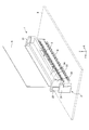
- FIG. 1 is a perspective view of a connector and a cable according to the embodiment.
- FIG. 2 is a perspective view of the connector according to the embodiment.
- FIG. 3 is a perspective view of the connector and cable of the embodiment.
- FIG. 4 is a perspective view of the connector according to the embodiment.
- FIG. 5 is a left side view of the connector and cable of the embodiment.
- FIG. 6 is a plan view of the connector and cable of the embodiment.
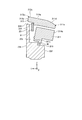
- 7 is a cross-sectional view taken along the line AA in FIG.
- FIG. 8 is a plan view of the side wall with the actuator properly closed.
- FIG. 9 is a plan view of the side wall with the actuator not properly closed.
- 10 is a cross-sectional view taken along the line BB of FIG.
- FIG. 11 is a perspective view of a modified connector.
- FIG. 12 is a cross-sectional view of a modified connector.
- FIG. 1 is a perspective view of a connector and a cable according to the embodiment.
- FIG. 2 is a perspective view of the connector according to the embodiment.
- FIG. 3 is a perspective view of the connector and cable of the embodiment.
- FIG. 4 is a perspective view of the connector according to the embodiment.
- the connector 1 of the embodiment is a device for connecting a cable 8 and a substrate 9.
- the connector 1 is fixed to the substrate 9.
- the cable 8 is a flexible circuit board (Flexible Printed Circuit: FPC) or a flexible flat cable (Flexible Flat Cable: FFC).
- the cable 8 is a flexible thin plate-like cable.
- the board 9 is a printed board and includes a plurality of electronic components.
- an XYZ orthogonal coordinate system is used.
- the Z axis is orthogonal to the substrate 9.
- the X axis is parallel to the longitudinal direction of the connector 1.
- the Y axis is orthogonal to both the X axis and the Z axis.
- the direction along the X axis is described as the X direction
- the direction along the Y axis is described as the Y direction
- the direction along the Z axis is described as the Z direction.
- a direction from the substrate 9 toward the connector 1 in the Z direction is defined as a + Z direction.
- a direction from the cable 8 toward an insulator 2 described later is defined as a + Y direction.
- the + X direction is the right direction when the + Y direction is viewed from the + Y direction.
- a plurality of contacts 4, an insulator 2, and an actuator 3 are provided.
- the plurality of contacts 4 are held by the insulator 2.
- the plurality of contacts 4 are arranged at a predetermined interval in the X direction.
- the contact 4 is fixed to the substrate 9.
- the contact 4 holds the cable 8.
- the contact 4 electrically connects the substrate 9 and the cable 8.
- FIG. 5 is a left side view of the connector and cable of the embodiment.
- FIG. 6 is a plan view of the connector and cable of the embodiment.
- 7 is a cross-sectional view taken along the line AA in FIG.
- the insulator 2 includes two end walls 21 and a rear wall 23.
- the end wall 21 has a plate shape orthogonal to the X axis.
- the rear wall 23 has a plate shape orthogonal to the Y axis.
- the two end walls 21 are connected by a rear wall 23.
- the rear wall 23 includes an upper surface 23a, a first main surface 23c, a back surface 23b, and a front surface 23f.
- the upper surface 23a is a surface that is orthogonal to the Z axis and faces the + Z direction.
- the first major surface 23c is a surface that is orthogonal to the Y axis and faces the -Y direction.
- the first main surface 23 c is a surface facing the cable 8.
- the back surface 23b is a surface that is orthogonal to the Y axis and faces the + Y direction.
- the back surface 23b is a surface opposite to the first main surface 23c.
- the front surface 23f is a surface that is orthogonal to the Y axis and faces the -Y direction.
- the front surface 23f is the surface farthest from the back surface 23b.
- the rear wall 23 includes two recesses 235.
- the recess 235 is a groove provided in the upper surface 23a.
- Actuator 3 is attached to insulator 2.
- the actuator 3 can rotate with respect to the insulator 2.
- the actuator 3 rotates around the rotation axis R shown in FIG.
- the rotation axis R is parallel to the X axis. That is, the rotation axis R is parallel to the substrate 9.
- the actuator 3 includes two side walls 31, a first plate 33, and a second plate 34.
- the side wall 31 has a plate shape orthogonal to the X axis.
- the first plate 33 has a plate shape orthogonal to the side wall 31.
- the second plate 34 has a plate shape orthogonal to the side wall 31 and the first plate 33.
- the two side walls 31 are connected by a first plate 33 and a second plate 34. The first plate 33 and the second plate 34 improve the strength of the actuator 3.
- the two side walls 31 When viewed from the Z direction, the two side walls 31 are arranged at positions displaced from the contacts 4. That is, the two side walls 31 do not overlap the contact 4 in plan view.
- the side wall 31 on the + X direction side is located in the + X direction with respect to the contact 4 located at the end on the + X direction side among the plurality of contacts 4.
- the side wall 31 on the ⁇ X direction side is located in the ⁇ X direction with respect to the contact 4 located at the end on the ⁇ X direction side among the plurality of contacts 4.
- the side wall 31 includes a base portion 311, a shaft 319, a recognition portion 313, and a convex portion 315.
- the base 311 includes an upper surface 311a, a second main surface 311c, a second end surface 311b, a curved surface 311d, and a second ridgeline 311e.
- the second main surface 311c is a surface that faces the first main surface 23c when the actuator 3 is rotated in a direction approaching the cable 8.
- the second end surface 311b is a surface located on the opposite side to the second main surface 311c.
- the second end surface 311b is parallel to the second main surface 311c.
- the curved surface 311d connects the second end surface 311b and the upper surface 311a. When viewed from the X direction, the curved surface 311d draws an arc centered on the rotation axis R.
- the second ridge line 311e is formed at a position where the curved surface 311d and the second end surface 311b intersect. That is, the second ridge line 311e is located at the end of the curved surface 311d and the end of the second end surface 311b.
- a state in which the second main surface 311c is parallel to the first main surface 23c is described as a first state.
- the state in which the second main surface 311c is orthogonal to the first main surface 23c is described as a second state.
- FIG. 2 and FIGS. 5 to 7 show the first state.
- the first state can also be said to be a state in which the actuator 3 is closed. 3 and 4 show the second state.
- the second state can also be said to be a state where the actuator 3 is opened.
- the cable 8 can be inserted between the insulator 2 and the actuator 3. After the cable 8 is inserted between the insulator 2 and the actuator 3, the actuator 3 is rotated in a direction approaching the cable 8.
- the actuator 3 rotates to a predetermined position, the actuator 3 is positioned by a lock mechanism provided in the insulator 2.
- the upper surface 311a of the base 311 is orthogonal to the Z axis and faces the + Z direction.
- the second main surface 311c of the base 311 is orthogonal to the Y axis and faces the + Y direction.
- the second main surface 311 c faces the ear portion 81 of the cable 8.
- the second end surface 311b of the base 311 is orthogonal to the Y axis and faces the ⁇ Y direction.
- the second ridge line 311e is located at the end of the side wall 31 in the ⁇ Y direction.
- the distance L5 is larger than the distance L6.
- the distance L5 is a distance from the rotation axis R to the second end surface 311b in a direction orthogonal to the second main surface 311c (Y direction in the first state shown in FIG. 7).
- the distance L6 is a distance from the rotation axis R to the front surface 23f.
- the shaft 319 projects from the base 311 in the X direction.
- the shaft 319 is attached to the end wall 21 of the insulator 2.
- the actuator 3 rotates around the shaft 319.
- the rotation axis R is a straight line passing through the center of a cross section obtained by cutting the shaft 319 along a plane orthogonal to the X axis.
- the recognition part 313 protrudes from the base 311 in a direction orthogonal to the second main surface 311c.
- the recognition unit 313 protrudes from the base 311 in the + Y direction.
- the recognition unit 313 is positioned in the + Y direction with respect to the first main surface 23 c of the insulator 2 and fits into the recess 235.
- the recognition unit 313 protrudes from the back surface 23b of the insulator 2 in the + Y direction.
- the recognition unit 313 includes an upper surface 313a, a first end surface 313b, and a first ridge line 313e.
- the upper surface 313a is a surface on the side opposite to the rear wall 23 of the insulator 2 and has a planar shape.
- the upper surface 313a is connected to the upper surface 311a of the base 311.
- the first end surface 313b is a surface farthest from the rotation axis R in a direction orthogonal to the second main surface 311c.
- the angle formed by the upper surface 313a and the first end surface 313b is 90 °.
- the first ridge line 313e is formed at a position where the upper surface 313a and the first end surface 313b intersect.
- the first ridge line 313e is located at the end of the upper surface 313a and the end of the first end surface 313b.
- the distance from the second end surface 311b to the first end surface 313b (the length in the Y direction of the side wall 31 in the first state) is larger than the length in the Y direction of the end wall 21 of the insulator 2.
- the distance from the second end surface 311b to the first end surface 313b is desirably as large as possible.
- the upper surface 313a is orthogonal to the Z axis and faces the + Z direction.
- the first end face 313b is orthogonal to the Y axis and faces the + Y direction.
- the first ridge line 313e is located at the end of the side wall 31 in the + Y direction.
- the distance L1 is larger than the distance L2.
- the distance L1 is a distance from the rotation axis R to the tip of the recognition unit 313 (first end surface 313b) in a direction orthogonal to the second main surface 311c (Y direction in the first state shown in FIG. 7).
- the distance L2 is a distance from the rotation axis R to the back surface 23b.
- the upper surface 313a of the recognition unit 313 is displaced in the Z direction with respect to the upper surface 23a of the insulator 2.
- the distance L3 is larger than the distance L4.
- the distance L3 is from the rotation axis R in the direction orthogonal to the rotation axis R and parallel to the second main surface 311c (Z direction in the first state shown in FIG. 7) to the tip of the recognition unit 313 (upper surface 313a).
- the distance L4 is a distance from the rotation axis R to the upper surface 23a of the rear wall 23 in a direction perpendicular to the rotation axis R and parallel to the back surface 23b (Z direction in the first state shown in FIG. 7).
- the convex portion 315 protrudes from the base portion 311 in a direction orthogonal to the second main surface 311 c.
- the convex portion 315 In the first state, the convex portion 315 is located in the ⁇ Y direction with respect to the first main surface 23 c of the insulator 2 and is located in the ⁇ Z direction with respect to the concave portion 235.
- the convex portion 315 faces the first main surface 23c with a gap.
- the convex portion 315 covers the + Z direction side of the ear portion 81 of the cable 8. Thereby, the cable 8 is prevented from coming off.
- the first plate 33 is a member extending from one side wall 31 to the other side wall 31.
- the first plate 33 has a plate shape orthogonal to the second main surface 311c.
- the first plate 33 In the first state, the first plate 33 has a plate shape orthogonal to the Z axis.
- the first plate 33 includes a notch 331.
- the notch 331 overlaps at least one of the contacts 4 in the Z direction in the first state. Thereby, it becomes possible to confirm the mounting state of the contact 4 from the Z direction.
- the second plate 34 is a member extending from one side wall 31 to the other side wall 31.
- the second plate 34 has a plate shape orthogonal to the first plate 33.
- the second plate 34 In the first state, has a plate shape orthogonal to the Y axis.
- the first plate 33 and the second plate 34 improve the strength of the actuator 3.
- FIG. 8 is a plan view of the side wall with the actuator properly closed.
- FIG. 9 is a plan view of the side wall with the actuator not properly closed.
- 10 is a cross-sectional view taken along the line BB of FIG. 1 and 5 to 8 show a state in which the actuator 3 is correctly closed.
- the state in which the actuator 3 is properly closed is a state in which the convex portion 315 of the side wall 31 is positioned in the + Z direction with respect to the ear portion 81 of the cable 8 as shown in FIG.
- the state where the actuator 3 is not properly closed is a state where the convex portion 315 rides on the ⁇ Y direction of the ear portion 81 as shown in FIG.
- the actuator 3 may not be properly closed due to interference between the actuator 3 and the ear 81 of the cable 8 or the like.
- the actuator 3 that is not properly closed needs to be detected by product inspection or the like. For this reason, it is desirable that the connector 1 can easily determine whether or not the actuator 3 is properly closed by inspection.
- the convex portion 315 of the side wall 31 is positioned in the + Z direction with respect to the ear portion 81 of the cable 8 as shown in FIG.
- the second main surface 311c is parallel to the first main surface 23c.
- the recognition unit 313 protrudes in the + Y direction from the back surface 23 b of the insulator 2.
- the convex portion 315 of the side wall 31 interferes with the ear portion 81 of the cable 8. That is, the convex portion 315 rides on the ear portion 81 in the ⁇ Y direction.
- the second main surface 311c is not parallel to the first main surface 23c.
- the recognition unit 313 does not protrude from the back surface 23 b of the insulator 2. Or even if the recognition part 313 protrudes in + Y direction rather than the back surface 23b, compared with the case of FIG. 8, the protrusion amount becomes small.
- the connector 1 is automatically inspected by an inspection device.
- the inspection device is, for example, an automatic optical inspection device (AOI).
- the inspection apparatus scans the connector 1 with the camera from the + Z direction side.
- the inspection device determines whether or not the cable 8 is correctly connected based on the position of the recognition unit 313. For example, the inspection apparatus detects the position of the first ridge line 313e of the recognition unit 313 with respect to a predetermined reference line S1, as shown in FIGS.
- the reference line S1 is a straight line that overlaps the back surface 23b of the insulator 2, for example.
- the inspection apparatus determines that the cable 8 is correctly connected.
- FIG. 9 when the first ridge line 313e is located on the ⁇ Y direction side of the reference line S1, the inspection apparatus determines that the cable 8 is not correctly connected.
- the reference line S1 is not necessarily a straight line that overlaps the back surface 23b.
- the position of the reference line S1 is not particularly limited.
- the inspection apparatus may detect the protrusion amount of the recognition unit 313 with respect to the reference line S1. The inspection apparatus may determine whether or not the cable 8 is correctly connected based on the area occupied by the recognition unit 313 in an arbitrary region A1 as illustrated in FIGS.
- the inspection device determines whether the cable 8 is correctly connected based on the position of the base 311. For example, the inspection apparatus detects the position of the second ridge line 311e of the base 311 with respect to a predetermined reference line S2, as shown in FIGS. As shown in FIG. 8, when the second ridge line 311e is located on the + Y direction side of the reference line S1, the inspection apparatus determines that the cable 8 is correctly connected. As shown in FIG. 9, when the second ridge line 311e is located on the ⁇ Y direction side of the reference line S2, the inspection apparatus determines that the cable 8 is not correctly connected.
- the inspection apparatus may detect the protruding amount of the base 311 with respect to the reference line S2.
- the inspection apparatus may determine whether or not the cable 8 is correctly connected based on the area occupied by the base 311 in an arbitrary region A2 as shown in FIGS.
- the insulator 2 does not necessarily have to include the recess 235. However, it is desirable that the insulator 2 includes the recess 235 in that the recognition unit 313 is less likely to be displaced in the X direction from a predetermined position. Since the recognition unit 313 is positioned by the recess 235, the determination accuracy of the inspection apparatus is improved.
- the second end surface 311b may not be parallel to the second main surface 311c.
- the angle which the 2nd end surface 311b makes with respect to the upper surface 311a should just be 90 degrees or less.
- the angle formed between the upper surface 313a and the first end surface 313b may not be 90 °, but may be 90 ° or less.
- the two side walls 31 may overlap the contact 4 in plan view. However, it is preferable that the two side walls 31 do not overlap with the contact 4 in plan view in that it is easy to check the mounting state of the contact 4.
- the connector 1 may include an elastic member that pushes the actuator 3 away from the insulator 2.
- the elastic member is, for example, a spring formed of metal.
- the connector 1 includes the insulator 2, the contact 4, and the actuator 3.
- the insulator 2 includes a first main surface 23c that is a surface facing the cable 8, and a back surface 23b that is a surface opposite to the first main surface 23c.
- the contact 4 electrically connects the cable 8 and the substrate 9.
- the actuator 3 can rotate around a rotation axis R parallel to the substrate 9.
- the actuator 3 includes a plate-like side wall 31 that intersects the rotation axis R.
- the side wall 31 includes a base 311 provided with a second main surface 311c that is a surface facing the first main surface 23c when the actuator 3 is rotated in a direction approaching the cable 8, and a recognition unit 313 protruding from the base 311. Is provided.
- a distance L1 from the rotation axis R to the tip (first end surface 313b) of the recognition unit 313 in a direction orthogonal to the second main surface 311c is larger than a distance L2 from the rotation axis R to the back surface 23b.
- the recognition unit 313 protrudes from the insulator 2 in a plan view.
- the recognition unit 313 does not protrude from the insulator 2 in a plan view, or the amount of protrusion of the recognition unit 313 is small. Therefore, according to the connector 1, it can be easily determined by inspection whether or not the actuator 3 is properly closed.
- a distance L3 from the rotation axis R to the tip (upper surface 313a) of the recognition unit 313 in a direction orthogonal to the rotation axis R and parallel to the second main surface 311c is orthogonal to the rotation axis R.
- the distance L4 from the rotation axis R to the upper surface 23a of the insulator 2 in a direction parallel to the rear surface 23b is different.
- a distance L3 from the rotation axis R to the tip (upper surface 313a) of the recognition unit 313 in a direction orthogonal to the rotation axis R and parallel to the second main surface 311c is orthogonal to the rotation axis R.
- the distance L4 is larger than the distance L4 from the rotation axis R to the upper surface 23a of the insulator 2 in the direction parallel to the rear surface 23b.
- the recognition unit 313 includes a first end surface 313b that is a surface farthest from the rotation axis R in a direction orthogonal to the second main surface 311c, and a first ridge line 313e that is positioned at the end of the first end surface 313b. And comprising. Thereby, the position of the front-end
- the recognition unit 313 includes a top surface 313a that is a surface opposite to the insulator 2 and is planar. Thereby, the reflection in the recognition part 313 of the light irradiated from an inspection apparatus tends to become uniform. For this reason, according to the connector 1, it becomes easier to check whether or not the actuator 3 is properly closed.
- the insulator 2 includes a front surface 23f that is the surface farthest from the back surface 23b.
- the base 311 includes a second end surface 311b which is a surface located on the opposite side of the rotation axis R from the second main surface 311c.
- a distance L5 from the rotation axis R to the second end surface 311b in a direction orthogonal to the second main surface 311c is larger than a distance L6 from the rotation axis R to the front surface 23f.
- the connector 1 includes an insulator 2, a contact 4, and an actuator 3.
- the insulator 2 includes a first main surface 23c that is a surface facing the cable 8, a back surface 23b that is a surface opposite to the first main surface 23c, and a front surface 23f that is a surface farthest from the back surface 23b.
- the contact 4 electrically connects the cable 8 and the substrate 9.
- the actuator 3 can rotate around a rotation axis R parallel to the substrate 9.
- the actuator 3 includes a plate-like side wall 31 that intersects the rotation axis R.
- the side wall 31 is opposite to the second main surface 311c with respect to the rotation axis R and the second main surface 311c, which is the surface facing the first main surface 23c when the actuator 3 is rotated in the direction approaching the cable 8. And a second end face 311b which is a surface located on the side.
- a distance L5 from the rotation axis R to the second end surface 311b in a direction orthogonal to the second main surface 311c is larger than a distance L6 from the rotation axis R to the front surface 23f.
- the base 311 protrudes from the insulator 2 in a plan view.
- the actuator 3 is not properly closed, the base 311 does not protrude from the insulator 2 in a plan view or the protruding amount of the recognition unit 313 becomes small. Therefore, according to the connector 1, it can be easily determined by inspection whether or not the actuator 3 is properly closed.
- the base 311 includes a second ridgeline 311e located at the end of the second end surface 311b. Thereby, the position of the front-end
- the base 311 includes a curved surface 311d connected to the second end surface 311b.
- the curved surface 311d draws an arc centered on the rotation axis R.
- the curved surface 311d is an arc centered on the rotation axis R, so that the position from the camera to the photographing target portion is constant even if the actuator 3 is tilted to some extent. For this reason, even if the focus position of the camera is constant, the captured image tends to be clear. Therefore, the inspection accuracy as to whether or not the actuator 3 is properly closed is improved.
- FIG. 11 is a perspective view of a modified connector.
- FIG. 12 is a cross-sectional view of a modified connector. Note that the same components as those described in the above-described embodiment are denoted by the same reference numerals, and redundant description is omitted.
- the actuator 3A of the connector 1A includes a side wall 31A having a shape different from that of the side wall 31 described above.
- the base 311A of the side wall 31A includes a curved surface 311dA.
- the curved surface 311dA connects the second end surface 311b and the upper surface 311a.
- the base 311A does not include the second ridge line 311e described above at the end of the curved surface 311dA. That is, the curved surface 311dA and the second end surface 311b are smoothly connected.
- the base 311A may not include the second ridge line 311e. Even in such a case, the base 311A can be used for checking whether the actuator 3 is properly closed.
Abstract
コネクタは、ケーブルに面する表面である第1主面、及び第1主面とは反対側の表面である背面を備えるインシュレータと、ケーブルと基板とを電気的に接続するコンタクトと、基板に平行な回転軸を中心に回転できるアクチュエータと、を備える。アクチュエータは、回転軸に対して交差する板状の側壁を備える。側壁は、前記アクチュエータが前記ケーブルに近付く方向に回転させられた時に前記第1主面に面する表面である第2主面を備える基部と、基部から突出する認識部と、を備える。第2主面に対して直交する方向における、回転軸から認識部の先端までの距離は、回転軸から背面までの距離よりも大きい。
Description
本出願は、2018年2月26日に日本国に特許出願された特願2018-032234の優先権を主張するものであり、この出願の開示全体をここに参照のために取り込む。
本発明は、コネクタに関する。
フレキシブル回路基板(Flexible Printed Circuit:FPC)又はフレキシブルフラットケーブル(Flexible Flat Cable:FFC)等(以下、ケーブルという)を基板に接続するためにコネクタが用いられる。特許文献1にはコネクタの一例が記載されている。特許文献1のコネクタにおいては、ハウジングに対して回転できるカバー部材がケーブルの耳部を覆うことによって、ケーブルがハウジングから抜け出ることが防止される。
実施形態の一態様に係るコネクタは、ケーブルに面する表面である第1主面、及び前記第1主面とは反対側の表面である背面を備えるインシュレータと、前記ケーブルと基板とを電気的に接続するコンタクトと、前記基板に平行な回転軸を中心に回転できるアクチュエータと、を備える。前記アクチュエータは、前記回転軸に対して交差する板状の側壁を備える。前記側壁は、前記アクチュエータが前記ケーブルに近付く方向に回転させられた時に前記第1主面に面する表面である第2主面を備える基部と、前記基部から突出する認識部と、を備える。前記第2主面に対して直交する方向における、前記回転軸から前記認識部の先端までの距離は、前記回転軸から前記背面までの距離よりも大きい。
以下、本開示のコネクタの実施形態を図面に基づいて説明する。なお、この実施形態により発明が限定されるものではない。また、下記実施形態における構成要素には、当業者が置換可能かつ容易なもの、あるいは実質的に同一のものが含まれる。
(実施形態)
図1は、実施形態のコネクタ及びケーブルの斜視図である。図2は、実施形態のコネクタの斜視図である。図3は、実施形態のコネクタ及びケーブルの斜視図である。図4は、実施形態のコネクタの斜視図である。
図1は、実施形態のコネクタ及びケーブルの斜視図である。図2は、実施形態のコネクタの斜視図である。図3は、実施形態のコネクタ及びケーブルの斜視図である。図4は、実施形態のコネクタの斜視図である。
図1に示すように、実施形態のコネクタ1は、ケーブル8と基板9とを接続するための装置である。コネクタ1は、基板9に固定される。ケーブル8は、フレキシブル回路基板(Flexible Printed Circuit:FPC)又はフレキシブルフラットケーブル(Flexible Flat Cable:FFC)等である。ケーブル8は、可撓性を有する薄い板状のケーブルである。基板9は、プリント基板であり、複数の電子部品を備える。
以下の説明において、XYZ直交座標系が用いられる。Z軸は、基板9に対して直交する。X軸は、コネクタ1の長手方向に平行である。Y軸は、X軸及びZ軸の両方に対して直交する。X軸に沿う方向はX方向と記載され、Y軸に沿う方向はY方向と記載され、Z軸に沿う方向はZ方向と記載される。Z方向のうち、基板9からコネクタ1に向かう方向を+Z方向とする。Y方向のうち、ケーブル8から後述するインシュレータ2に向かう方向を+Y方向とする。+Z方向を上として+Y方向を見た場合の右方向を+X方向とする。
図2に示すように、複数のコンタクト4と、インシュレータ2と、アクチュエータ3と、を備える。複数のコンタクト4は、インシュレータ2に保持される。複数のコンタクト4は、X方向に所定の間隔を空けて並べられる。コンタクト4は、基板9に固定される。コンタクト4は、ケーブル8を把持する。コンタクト4は、基板9とケーブル8とを電気的に接続する。
図5は、実施形態のコネクタ及びケーブルの左側面図である。図6は、実施形態のコネクタ及びケーブルの平面図である。図7は、図6のA-A断面図である。
図4に示すように、インシュレータ2は、2つの端壁21と、後壁23と、を備える。端壁21は、X軸に対して直交する板状である。後壁23は、Y軸に対して直交する板状である。2つの端壁21は、後壁23によって接続されている。
図7に示すように、後壁23は、上面23aと、第1主面23cと、背面23bと、前面23fと、を備える。上面23aは、Z軸に対して直交し且つ+Z方向を向く表面である。第1主面23cは、Y軸に対して直交し且つ-Y方向を向く表面である。第1主面23cは、ケーブル8に面する表面である。背面23bは、Y軸に対して直交し且つ+Y方向を向く表面である。背面23bは、第1主面23cとは反対側の表面である。前面23fは、Y軸に対して直交し且つ-Y方向を向く表面である。前面23fは、背面23bから最も遠い表面である。また、図4及び図7に示すように、後壁23は、2つの凹部235を備える。凹部235は、上面23aに設けられた溝である。
アクチュエータ3は、インシュレータ2に取り付けられる。アクチュエータ3は、インシュレータ2に対して回転できる。アクチュエータ3は、図5に示す回転軸Rを中心に回転する。回転軸Rは、X軸と平行である。すなわち、回転軸Rは、基板9と平行である。
図2に示すように、アクチュエータ3は、2つの側壁31と、第1プレート33と、第2プレート34と、を備える。側壁31は、X軸に対して直交する板状である。第1プレート33は、側壁31に対して直交する板状である。第2プレート34は、側壁31及び第1プレート33に対して直交する板状である。2つの側壁31は、第1プレート33及び第2プレート34によって接続されている。第1プレート33及び第2プレート34によって、アクチュエータ3の強度が向上する。
Z方向から見て、2つの側壁31は、コンタクト4からずれた位置に配置されている。すなわち、2つの側壁31は、平面視でコンタクト4に重ならない。+X方向側の側壁31は、複数のコンタクト4のうち+X方向側の端部に位置するコンタクト4に対して、+X方向に位置する。-X方向側の側壁31は、複数のコンタクト4のうち-X方向側の端部に位置するコンタクト4に対して、-X方向に位置する。
図5及び図7に示すように、側壁31は、基部311と、シャフト319と、認識部313と、凸部315と、を備える。図7に示すように、基部311は、上面311aと、第2主面311cと、第2端面311bと、曲面311dと、第2稜線311eと、を備える。第2主面311cは、アクチュエータ3がケーブル8に近付く方向に回転させられた時に第1主面23cに面する表面である。第2端面311bは、第2主面311cとは反対側に位置する表面である。第2端面311bは、第2主面311cと平行である。曲面311dは、第2端面311b及び上面311aを繋ぐ。X方向から見て、曲面311dは、回転軸Rを中心とした円弧を描く。第2稜線311eは、曲面311dと第2端面311bとが交差する位置に形成される。すなわち、第2稜線311eは、曲面311dの端部及び第2端面311bの端部に位置する。
以下の説明において、第2主面311cが第1主面23cに平行である状態は、第1状態と記載される。第2主面311cが第1主面23cに対して直交する状態は、第2状態と記載される。図1、図2及び図5から図7は、第1状態を示す。第1状態は、アクチュエータ3が閉じた状態ともいえる。図3及び図4は、第2状態を示す。第2状態は、アクチュエータ3が開いた状態ともいえる。第2状態では、ケーブル8をインシュレータ2とアクチュエータ3との間に挿入することが可能である。ケーブル8がインシュレータ2とアクチュエータ3との間に挿入された後、アクチュエータ3がケーブル8に近付く方向へ回転させられる。アクチュエータ3が所定の位置まで回転すると、インシュレータ2に設けられたロック機構によってアクチュエータ3が位置決めされる。
図7に示すように、第1状態で、基部311の上面311aは、Z軸に対して直交し且つ+Z方向を向く。第1状態で、基部311の第2主面311cは、Y軸に対して直交し且つ+Y方向を向く。第1状態で、第2主面311cは、ケーブル8の耳部81に面する。第1状態で、基部311の第2端面311bは、Y軸に対して直交し且つ-Y方向を向く。第1状態で、第2稜線311eは、側壁31のうち-Y方向の端部に位置する。
図7に示すように、距離L5は、距離L6よりも大きい。距離L5は、第2主面311cに対して直交する方向(図7に示す第1状態でY方向)における、回転軸Rから第2端面311bまでの距離である。距離L6は、回転軸Rから前面23fまでの距離である。
図6に示すように、シャフト319は、基部311からX方向に突出する。シャフト319は、インシュレータ2の端壁21に取り付けられる。アクチュエータ3は、シャフト319を中心に回転する。回転軸Rは、シャフト319をX軸に対して直交する平面で切った断面の中心を通る直線である。
図7に示すように、認識部313は、基部311から、第2主面311cに対して直交する方向に突出する。図7に示すように、第1状態で、認識部313は、基部311から+Y方向に突出する。第1状態で、認識部313は、インシュレータ2の第1主面23cに対して+Y方向に位置し、凹部235に嵌まる。第1状態で、認識部313は、インシュレータ2の背面23bから+Y方向に突出する。
図7に示すように、認識部313は、上面313aと、第1端面313bと、第1稜線313eと、を備える。上面313aは、インシュレータ2の後壁23とは反対側の表面であって、平面状である。上面313aは、基部311の上面311aと繋がっている。第1端面313bは、第2主面311cに対して直交する方向で回転軸Rから最も遠い表面である。上面313aと第1端面313bとがなす角度は、90°である。第1稜線313eは、上面313aと第1端面313bとが交差する位置に形成される。すなわち、第1稜線313eは、上面313aの端部及び第1端面313bの端部に位置する。第2端面311bから第1端面313bまでの距離(第1状態での側壁31のY方向の長さ)は、インシュレータ2の端壁21のY方向の長さよりも大きい。第2端面311bから第1端面313bまでの距離は、できるだけ大きい方が望ましい。
図7に示すように、第1状態で、上面313aは、Z軸に対して直交し且つ+Z方向を向く。第1状態で、第1端面313bは、Y軸に対して直交し且つ+Y方向を向く。第1状態で、第1稜線313eは、側壁31のうち+Y方向の端部に位置する。
図7に示すように、距離L1は、距離L2よりも大きい。距離L1は、第2主面311cに対して直交する方向(図7に示す第1状態でY方向)における、回転軸Rから認識部313の先端(第1端面313b)までの距離である。距離L2は、回転軸Rから背面23bまでの距離である。
図7に示すように、認識部313の上面313aは、インシュレータ2の上面23aに対してZ方向にずれている。図7に示すように、距離L3は、距離L4よりも大きい。距離L3は、回転軸Rに対して直交し且つ第2主面311cと平行な方向(図7に示す第1状態でZ方向)における回転軸Rから認識部313の先端(上面313a)までの距離である。距離L4は、回転軸Rに対して直交し且つ背面23bと平行な方向(図7に示す第1状態でZ方向)における、回転軸Rから後壁23の上面23aまでの距離である。
図7に示すように、凸部315は、基部311から、第2主面311cに対して直交する方向に突出する。第1状態で、凸部315は、インシュレータ2の第1主面23cに対して-Y方向に位置し、且つ凹部235に対して-Z方向に位置する。第1状態で、凸部315は、第1主面23cに隙間を空けて対向する。第1状態で、凸部315は、ケーブル8の耳部81の+Z方向側を覆う。これにより、ケーブル8が抜け止めされる。
図2に示すように、第1プレート33は、一方の側壁31から他方の側壁31に亘る部材である。第1プレート33は、第2主面311cに対して直交する板状である。第1状態で、第1プレート33は、Z軸に対して直交する板状である。図6に示すように、第1プレート33は、は、切欠き331を備える。切欠き331は、第1状態においてZ方向でコンタクト4の少なくとも1つに重なる。これにより、Z方向からコンタクト4の実装状態を確認することが可能となる。
第2プレート34は、一方の側壁31から他方の側壁31に亘る部材である。第2プレート34は、第1プレート33に対して直交する板状である。第1状態で、第2プレート34は、Y軸に対して直交する板状である。第1プレート33及び第2プレート34によってアクチュエータ3の強度が向上する。
図8は、アクチュエータが正しく閉じられている状態の側壁の平面図である。図9は、アクチュエータが正しく閉じられていない状態の側壁の平面図である。図10は、図9のB-B断面図である。図1及び図5から図8は、アクチュエータ3が正しく閉じられている状態を示す。アクチュエータ3が正しく閉じられている状態とは、図7に示すように、側壁31の凸部315がケーブル8の耳部81よりも+Z方向に位置する状態である。アクチュエータ3が正しく閉じられていない状態とは、図10に示すように、凸部315が耳部81の-Y方向に乗り上げた状態である。
ケーブル8が正しい位置に配置されなかった場合、アクチュエータ3とケーブル8の耳部81との干渉等によってアクチュエータ3が正しく閉まらないことがある。正しく閉まっていないアクチュエータ3は、製品検査等で検出する必要がある。このため、コネクタ1においては、アクチュエータ3が正しく閉まっているか否かを検査で容易に判定できることが望ましい。
ケーブル8が正しい位置に配置された場合、図7に示すように、側壁31の凸部315がケーブル8の耳部81よりも+Z方向に位置する。この場合、第2主面311cが第1主面23cと平行になる。このため、図8に示すように、認識部313が、インシュレータ2の背面23bよりも+Y方向に突出する。
一方、ケーブル8が正しい位置に配置されなかった場合、側壁31の凸部315がケーブル8の耳部81と干渉する。すなわち、凸部315が耳部81の-Y方向に乗り上げる。この場合、第2主面311cが第1主面23cと平行にならない。このため、例えば図9に示すように、認識部313が、インシュレータ2の背面23bから突出しない。又は、認識部313が背面23bよりも+Y方向に突出したとしても、図8の場合と比較して突出量が小さくなる。
ケーブル8が接続されたコネクタ1に対して、ケーブル8が正しく接続されているか否かを判定する製品検査が行われる。コネクタ1は、検査装置によって自動的に検査される。検査装置は、例えば自動光学検査装置(Automated Optical Inspection:AOI)である。検査装置は、+Z方向側からコネクタ1をカメラでスキャンする。
検査装置は、認識部313の位置に基づいて、ケーブル8が正しく接続されているか否かを判定する。例えば、検査装置は、図8及び図9に示すように所定の基準線S1に対する認識部313の第1稜線313eの位置を検出する。基準線S1は、例えばインシュレータ2の背面23bに重なる直線である。図8に示すように第1稜線313eが基準線S1よりも+Y方向側に位置する場合に、検査装置は、ケーブル8が正しく接続されていると判定する。図9に示すように第1稜線313eが基準線S1よりも-Y方向側に位置する場合に、検査装置は、ケーブル8が正しく接続されていないと判定する。
なお、基準線S1は、必ずしも背面23bに重なる直線でなくてもよい。基準線S1の位置は、特に限定されない。また、検査装置は、基準線S1に対する認識部313の突出量を検出してもよい。検査装置は、図8及び図9に示すような任意の領域A1において認識部313が占める面積に基づいて、ケーブル8が正しく接続されているか否かを判定してもよい。
検査装置は、基部311の位置に基づいて、ケーブル8が正しく接続されているか否かを判定する。例えば、検査装置は、図8及び図9に示すように所定の基準線S2に対する基部311の第2稜線311eの位置を検出する。図8に示すように第2稜線311eが基準線S1よりも+Y方向側に位置する場合に、検査装置は、ケーブル8が正しく接続されていると判定する。図9に示すように第2稜線311eが基準線S2よりも-Y方向側に位置する場合に、検査装置は、ケーブル8が正しく接続されていないと判定する。
なお、基準線S2の位置は、特に限定されない。また、検査装置は、基準線S2に対する基部311の突出量を検出してもよい。検査装置は、図8及び図9に示すような任意の領域A2において基部311が占める面積に基づいて、ケーブル8が正しく接続されているか否かを判定してもよい。
インシュレータ2は、必ずしも凹部235を備えていなくてもよい。ただし、認識部313が所定の位置からX方向にずれにくくなる点で、インシュレータ2が凹部235を備える方が望ましい。認識部313が凹部235によって位置決めされることによって、検査装置の判定精度が向上する。
アクチュエータ3の基部311において、第2端面311bは、第2主面311cと平行でなくてもよい。第2端面311bが上面311aに対してなす角度が90°以下であればよい。認識部313において、上面313aと第1端面313bとがなす角度は、90°でなくてもよく、90°以下であればよい。
2つの側壁31は、平面視でコンタクト4と重なっていてもよい。ただし、コンタクト4の実装状態を確認しやすくなる点で、2つの側壁31が平面視でコンタクト4と重なっていない方が望ましい。
コネクタ1は、アクチュエータ3をインシュレータ2から遠ざかる方向に押す弾性部材を備えていてもよい。弾性部材は、例えば金属で形成されたバネである。
以上で説明したように、コネクタ1は、インシュレータ2と、コンタクト4と、アクチュエータ3と、を備える。インシュレータ2は、ケーブル8に面する表面である第1主面23c、及び第1主面23cとは反対側の表面である背面23bを備える。コンタクト4は、ケーブル8と基板9とを電気的に接続する。アクチュエータ3は、基板9と平行な回転軸Rを中心に回転できる。アクチュエータ3は、回転軸Rに対して交差する板状の側壁31を備える。側壁31は、アクチュエータ3がケーブル8に近付く方向に回転させられた時に第1主面23cに面する表面である第2主面311cを備える基部311と、基部311から突出する認識部313と、を備える。第2主面311cに対して直交する方向における、回転軸Rから認識部313の先端(第1端面313b)までの距離L1は、回転軸Rから背面23bまでの距離L2よりも大きい。
これにより、アクチュエータ3が正しく閉まっていれば、平面視で認識部313がインシュレータ2から突出する。一方、アクチュエータ3が正しく閉まっていなければ、平面視で認識部313がインシュレータ2から突出しないか、認識部313の突出量が小さくなる。したがって、コネクタ1によれば、アクチュエータ3が正しく閉まっているか否かを検査で容易に判定できる。
コネクタ1において、回転軸Rに対して直交し且つ第2主面311cと平行な方向における、回転軸Rから認識部313の先端(上面313a)までの距離L3は、回転軸Rに対して直交し且つ背面23bと平行な方向における、回転軸Rからインシュレータ2の上面23aまでの距離L4とは異なる。これにより、検査装置のカメラのピントを認識部313に合わせ且つインシュレータ2の上面23aからずらすことが可能となる。このため、検査装置がインシュレータ2の上面23aを認識部313と誤認識することが抑制される。
コネクタ1において、回転軸Rに対して直交し且つ第2主面311cと平行な方向における、回転軸Rから認識部313の先端(上面313a)までの距離L3は、回転軸Rに対して直交し且つ背面23bと平行な方向における、回転軸Rからインシュレータ2の上面23aまでの距離L4よりも大きい。これにより、回転軸Rから認識部313までの距離が大きくなる。このため、アクチュエータ3が正しく閉まっていない場合の認識部313の位置ずれが大きくなりやすい。したがって、コネクタ1によれば、アクチュエータ3が正しく閉まっているか否かの検査がより容易になる。
コネクタ1において、認識部313は、第2主面311cに対して直交する方向において回転軸Rから最も遠い表面である第1端面313bと、第1端面313bの端部に位置する第1稜線313eと、を備える。これにより、平面視において認識部313の先端の位置が明確になる。このため、コネクタ1によれば、アクチュエータ3が正しく閉まっているか否かの検査がより容易になる。
コネクタ1において、認識部313は、インシュレータ2とは反対側の表面であって平面状である上面313aを備える。これにより、検査装置から照射される光の認識部313での反射が一様になりやすい。このため、コネクタ1によれば、アクチュエータ3が正しく閉まっているか否かの検査がより容易になる。
コネクタ1において、インシュレータ2は、背面23bから最も遠い表面である前面23fを備える。基部311は、回転軸Rに対して第2主面311cとは反対側に位置する表面である第2端面311bを備える。第2主面311cに対して直交する方向における、回転軸Rから第2端面311bまでの距離L5は、回転軸Rから前面23fまでの距離L6よりも大きい。
言い換えると、以下の通りである。コネクタ1は、インシュレータ2と、コンタクト4と、アクチュエータ3と、を備える。インシュレータ2は、ケーブル8に面する表面である第1主面23c、第1主面23cとは反対側の表面である背面23b、及び背面23bから最も遠い表面である前面23fを備える。コンタクト4は、ケーブル8と基板9とを電気的に接続する。アクチュエータ3は、基板9と平行な回転軸Rを中心に回転できる。アクチュエータ3は、回転軸Rに対して交差する板状の側壁31を備える。側壁31は、アクチュエータ3がケーブル8に近付く方向に回転させられた時に第1主面23cに面する表面である第2主面311cと、回転軸Rに対して第2主面311cとは反対側に位置する表面である第2端面311bと、を備える。第2主面311cに対して直交する方向における、回転軸Rから第2端面311bまでの距離L5は、回転軸Rから前面23fまでの距離L6よりも大きい。
これにより、アクチュエータ3が正しく閉まっていれば、平面視で基部311がインシュレータ2から突出する。一方、アクチュエータ3が正しく閉まっていなければ、平面視で基部311がインシュレータ2から突出しないか、認識部313の突出量が小さくなる。したがって、コネクタ1によれば、アクチュエータ3が正しく閉まっているか否かを検査で容易に判定できる。
コネクタ1において、基部311は、第2端面311bの端部に位置する第2稜線311eを備える。これにより、平面視において基部311の先端の位置が明確になる。このため、コネクタ1によれば、アクチュエータ3が正しく閉まっているか否かの検査がより容易になる。
コネクタ1において、基部311は、第2端面311bに繋がる曲面311dを備える。回転軸Rと平行な方向から見て、曲面311dは、回転軸Rを中心とした円弧を描く。これにより、アクチュエータ3の回転角度に関わらず、検査装置から照射される光の曲面311dでの反射が一定となる。したがって、コネクタ1によれば、アクチュエータ3が正しく閉まっているか否かの検査がより容易になる。また、検査装置のカメラのピント位置は、一定であることが望ましい。例えばカメラが曲面311dの一部を撮影する場合、曲面311dが回転軸Rを中心とした円弧であることによって、アクチュエータ3がある程度傾いていてもカメラから撮影対象部分までの位置が一定となる。このため、カメラのピント位置が一定であっても、撮影した画像が鮮明になりやすい。したがって、アクチュエータ3が正しく閉まっているか否かの検査精度が向上する。
本開示の実施形態は、発明の要旨及び範囲を逸脱しない範囲で変更することができる。さらに、本開示の実施形態及びその変形例は、適宜組み合わせることができる。例えば、上記の実施形態は、以下のように変形してもよい。
図11は、変形例のコネクタの斜視図である。図12は、変形例のコネクタの断面図である。なお、上述した実施形態で説明したものと同じ構成要素には同一の符号を付して重複する説明は省略する。
図11及び図12に示すように、変形例のコネクタ1Aのアクチュエータ3Aは、上述した側壁31とは異なる形状を有する側壁31Aを備える。図12に示すように、側壁31Aの基部311Aは、曲面311dAを備える。曲面311dAは、第2端面311b及び上面311aを繋ぐ。基部311Aは、曲面311dAの端部に上述した第2稜線311eを備えない。すなわち、曲面311dAと第2端面311bとが滑らかに繋がっている。このように、基部311Aは、第2稜線311eを備えなくてもよい。このような場合であっても、アクチュエータ3が正しく閉まっているか否かの検査に基部311Aを用いることは可能である。
1、1A コネクタ
2 インシュレータ
21 端壁
23 後壁
235 凹部
23a 上面
23b 背面
23c 第1主面
23f 前面
3、3A アクチュエータ
31、31A 側壁
311 基部
311a 上面
311b 第2端面
311c 第2主面
311d 曲面
311e 第2稜線
313 認識部
313a 上面
313b 第1端面
313e 第1稜線
315 凸部
319 シャフト
33 第1プレート
34 第2プレート
4 コンタクト
8 ケーブル
81 耳部
9 基板
2 インシュレータ
21 端壁
23 後壁
235 凹部
23a 上面
23b 背面
23c 第1主面
23f 前面
3、3A アクチュエータ
31、31A 側壁
311 基部
311a 上面
311b 第2端面
311c 第2主面
311d 曲面
311e 第2稜線
313 認識部
313a 上面
313b 第1端面
313e 第1稜線
315 凸部
319 シャフト
33 第1プレート
34 第2プレート
4 コンタクト
8 ケーブル
81 耳部
9 基板
Claims (8)
- ケーブルに面する表面である第1主面、及び前記第1主面とは反対側の表面である背面を備えるインシュレータと、
前記ケーブルと基板とを電気的に接続するコンタクトと、
前記基板に平行な回転軸を中心に回転できるアクチュエータと、
を備え、
前記アクチュエータは、前記回転軸に対して交差する板状の側壁を備え、
前記側壁は、前記アクチュエータが前記ケーブルに近付く方向に回転させられた時に前記第1主面に面する表面である第2主面を備える基部と、前記基部から突出する認識部と、を備え、
前記第2主面に対して直交する方向における、前記回転軸から前記認識部の先端までの距離は、前記回転軸から前記背面までの距離よりも大きい
コネクタ。 - 前記回転軸に対して直交し且つ前記第2主面と平行な方向における、前記回転軸から前記認識部の先端までの距離は、前記回転軸に対して直交し且つ前記背面と平行な方向における、前記回転軸から前記インシュレータの上面までの距離とは異なる
請求項1に記載のコネクタ。 - 前記回転軸に対して直交し且つ前記第2主面と平行な方向における、前記回転軸から前記認識部の先端までの距離は、前記回転軸に対して直交し且つ前記背面と平行な方向における、前記回転軸から前記インシュレータの上面までの距離よりも大きい
請求項1に記載のコネクタ。 - 前記認識部は、前記第2主面に対して直交する方向において前記回転軸から最も遠い表面である第1端面と、前記第1端面の端部に位置する第1稜線と、を備える
請求項1から3のいずれか1項に記載のコネクタ。 - 前記認識部は、前記インシュレータとは反対側の表面であって平面状である上面を備える
請求項1から4のいずれか1項に記載のコネクタ。 - 前記インシュレータは、前記背面から最も遠い表面である前面を備え、
前記基部は、前記回転軸に対して前記第2主面とは反対側に位置する表面である第2端面を備え、
前記第2主面に対して直交する方向における、前記回転軸から前記第2端面までの距離は、前記回転軸から前記前面までの距離よりも大きい
請求項1から5のいずれか1項に記載のコネクタ。 - 前記基部は、前記第2端面の端部に位置する第2稜線を備える
請求項6に記載のコネクタ。 - 前記基部は、前記第2端面に繋がる曲面を備え、
前記回転軸と平行な方向から見て、前記曲面は、前記回転軸を中心とした円弧を描く
請求項6又は7に記載のコネクタ。
Priority Applications (4)
| Application Number | Priority Date | Filing Date | Title |
|---|---|---|---|
| CN201980012860.8A CN111712972B (zh) | 2018-02-26 | 2019-02-07 | 连接器 |
| EP19757344.7A EP3761457B1 (en) | 2018-02-26 | 2019-02-07 | Connector |
| KR1020207024522A KR102390861B1 (ko) | 2018-02-26 | 2019-02-07 | 커넥터 |
| US16/975,569 US11245211B2 (en) | 2018-02-26 | 2019-02-07 | Connector having an actuator |
Applications Claiming Priority (2)
| Application Number | Priority Date | Filing Date | Title |
|---|---|---|---|
| JP2018-032234 | 2018-02-26 | ||
| JP2018032234A JP6552659B1 (ja) | 2018-02-26 | 2018-02-26 | コネクタ |
Publications (1)
| Publication Number | Publication Date |
|---|---|
| WO2019163539A1 true WO2019163539A1 (ja) | 2019-08-29 |
Family
ID=67473246
Family Applications (1)
| Application Number | Title | Priority Date | Filing Date |
|---|---|---|---|
| PCT/JP2019/004484 WO2019163539A1 (ja) | 2018-02-26 | 2019-02-07 | コネクタ |
Country Status (6)
| Country | Link |
|---|---|
| US (1) | US11245211B2 (ja) |
| EP (1) | EP3761457B1 (ja) |
| JP (1) | JP6552659B1 (ja) |
| KR (1) | KR102390861B1 (ja) |
| CN (1) | CN111712972B (ja) |
| WO (1) | WO2019163539A1 (ja) |
Citations (5)
| Publication number | Priority date | Publication date | Assignee | Title |
|---|---|---|---|---|
| JPH01315976A (ja) * | 1988-05-05 | 1989-12-20 | Amp Inc | 無挿入力電気コネクタ |
| US5795172A (en) * | 1996-12-18 | 1998-08-18 | Intel Corporation | Production printed circuit board (PCB) edge connector test connector |
| JP2005005210A (ja) * | 2003-06-13 | 2005-01-06 | Taiko Denki Co Ltd | 縦型コネクタ |
| JP2005135679A (ja) * | 2003-10-29 | 2005-05-26 | Taiko Denki Co Ltd | 扁平導体用コネクタ |
| JP2014026765A (ja) * | 2012-07-25 | 2014-02-06 | Molex Inc | コネクタ |
Family Cites Families (13)
| Publication number | Priority date | Publication date | Assignee | Title |
|---|---|---|---|---|
| US6790074B1 (en) * | 2003-03-14 | 2004-09-14 | P-Two Industries Inc. | Electrical power connector for flexible circuit board |
| TWM288981U (en) * | 2005-06-28 | 2006-03-21 | Compal Electronics Inc | Connector |
| JP4542525B2 (ja) * | 2005-07-07 | 2010-09-15 | 山一電機株式会社 | ケーブル用コネクタ |
| US20070054558A1 (en) * | 2005-09-03 | 2007-03-08 | Harlan Tod M | Connector with improved pulling portion |
| JP5020899B2 (ja) * | 2008-06-20 | 2012-09-05 | モレックス インコーポレイテド | 電気コネクタ |
| US7854625B1 (en) * | 2010-06-15 | 2010-12-21 | Cheng Uei Precision Industry Co., Ltd. | Connector for flexible printed circuit board |
| TW201324975A (zh) * | 2011-12-13 | 2013-06-16 | Aces Electronic Co Ltd | 電連接器 |
| JP2013178892A (ja) * | 2012-02-28 | 2013-09-09 | Kyocera Connector Products Corp | ケーブル用コネクタ |
| JP5571837B1 (ja) * | 2013-08-21 | 2014-08-13 | イリソ電子工業株式会社 | 電気コネクタ |
| US9680244B1 (en) * | 2014-09-09 | 2017-06-13 | Universal Lighting Technologies, Inc | Header apparatus for providing electrical connection to a printed circuit board, and daughter card and circuit assembly incorporating the header apparatus |
| JP6282565B2 (ja) * | 2014-09-22 | 2018-02-21 | 京セラ株式会社 | ケーブル用コネクタ |
| JP6336941B2 (ja) * | 2015-04-01 | 2018-06-06 | モレックス エルエルシー | コネクタ及びその製造方法 |
| JP6308197B2 (ja) * | 2015-11-10 | 2018-04-11 | 第一精工株式会社 | 電気コネクタ |
-
2018
- 2018-02-26 JP JP2018032234A patent/JP6552659B1/ja active Active
-
2019
- 2019-02-07 WO PCT/JP2019/004484 patent/WO2019163539A1/ja unknown
- 2019-02-07 CN CN201980012860.8A patent/CN111712972B/zh active Active
- 2019-02-07 KR KR1020207024522A patent/KR102390861B1/ko active IP Right Grant
- 2019-02-07 EP EP19757344.7A patent/EP3761457B1/en active Active
- 2019-02-07 US US16/975,569 patent/US11245211B2/en active Active
Patent Citations (5)
| Publication number | Priority date | Publication date | Assignee | Title |
|---|---|---|---|---|
| JPH01315976A (ja) * | 1988-05-05 | 1989-12-20 | Amp Inc | 無挿入力電気コネクタ |
| US5795172A (en) * | 1996-12-18 | 1998-08-18 | Intel Corporation | Production printed circuit board (PCB) edge connector test connector |
| JP2005005210A (ja) * | 2003-06-13 | 2005-01-06 | Taiko Denki Co Ltd | 縦型コネクタ |
| JP2005135679A (ja) * | 2003-10-29 | 2005-05-26 | Taiko Denki Co Ltd | 扁平導体用コネクタ |
| JP2014026765A (ja) * | 2012-07-25 | 2014-02-06 | Molex Inc | コネクタ |
Non-Patent Citations (1)
| Title |
|---|
| See also references of EP3761457A4 * |
Also Published As
| Publication number | Publication date |
|---|---|
| EP3761457A4 (en) | 2021-11-24 |
| KR102390861B1 (ko) | 2022-04-26 |
| EP3761457A1 (en) | 2021-01-06 |
| KR20200110434A (ko) | 2020-09-23 |
| US11245211B2 (en) | 2022-02-08 |
| CN111712972A (zh) | 2020-09-25 |
| CN111712972B (zh) | 2021-12-28 |
| US20200403339A1 (en) | 2020-12-24 |
| JP6552659B1 (ja) | 2019-07-31 |
| EP3761457B1 (en) | 2024-01-03 |
| JP2019149253A (ja) | 2019-09-05 |
Similar Documents
| Publication | Publication Date | Title |
|---|---|---|
| JP4562538B2 (ja) | モジュール用ソケット | |
| US8310536B2 (en) | Shape measurement apparatus and shape measurement method | |
| JP2007122966A (ja) | コネクタ | |
| JP2006073206A (ja) | Ffc用コネクタ | |
| KR101862009B1 (ko) | 고속 신호 전송용 플렉시블 케이블 커넥터 | |
| US7165991B2 (en) | Connector | |
| US20190343375A1 (en) | Three-dimensional wiring substrate and imaging unit | |
| JP2011097158A (ja) | カメラモジュール実装構造 | |
| WO2019163539A1 (ja) | コネクタ | |
| US6287021B1 (en) | Apparatus for coupling electronic components within electronic devices such as cameras | |
| US8526070B2 (en) | Document reading apparatus | |
| JP2021039175A (ja) | ドラムカートリッジ及び画像形成装置 | |
| CN109752814B (zh) | 镜头驱动装置、摄影模块与电子装置 | |
| US6912300B1 (en) | Irregular pattern reader | |
| KR102340537B1 (ko) | 멀티 카메라 모듈 | |
| JP2012037336A (ja) | 検査装置 | |
| US20040001304A1 (en) | Mechanism for inserting and removing electronic circuit unit | |
| KR20210098722A (ko) | 인쇄 회로 기판을 포함하는 전자 장치 | |
| JP2004213934A (ja) | 接続部品、及びコネクタ装置 | |
| US10608360B2 (en) | Circuit board-mounted electrical connector | |
| US20230180416A1 (en) | Sensor provided with plurality of circuit boards | |
| KR20030071533A (ko) | 위치검출방법, 위치검출장치 및 프린트 기판의 위치결정방법 | |
| TWI584053B (zh) | Aperture devices and cameras | |
| US20240012266A1 (en) | Optical unit with shake correction function | |
| JP6833579B2 (ja) | 操作部品および電子機器 |
Legal Events
| Date | Code | Title | Description |
|---|---|---|---|
| 121 | Ep: the epo has been informed by wipo that ep was designated in this application |
Ref document number: 19757344 Country of ref document: EP Kind code of ref document: A1 |
|
| ENP | Entry into the national phase |
Ref document number: 20207024522 Country of ref document: KR Kind code of ref document: A |
|
| NENP | Non-entry into the national phase |
Ref country code: DE |
|
| ENP | Entry into the national phase |
Ref document number: 2019757344 Country of ref document: EP Effective date: 20200928 |