WO2019155709A1 - 固体撮像素子、電子装置、および、電子装置の製造方法 - Google Patents
固体撮像素子、電子装置、および、電子装置の製造方法 Download PDFInfo
- Publication number
- WO2019155709A1 WO2019155709A1 PCT/JP2018/042049 JP2018042049W WO2019155709A1 WO 2019155709 A1 WO2019155709 A1 WO 2019155709A1 JP 2018042049 W JP2018042049 W JP 2018042049W WO 2019155709 A1 WO2019155709 A1 WO 2019155709A1
- Authority
- WO
- WIPO (PCT)
- Prior art keywords
- layer
- surface layer
- state imaging
- solid
- light
- Prior art date
- Legal status (The legal status is an assumption and is not a legal conclusion. Google has not performed a legal analysis and makes no representation as to the accuracy of the status listed.)
- Ceased
Links
Images














Classifications
-
- H—ELECTRICITY
- H10—SEMICONDUCTOR DEVICES; ELECTRIC SOLID-STATE DEVICES NOT OTHERWISE PROVIDED FOR
- H10F—INORGANIC SEMICONDUCTOR DEVICES SENSITIVE TO INFRARED RADIATION, LIGHT, ELECTROMAGNETIC RADIATION OF SHORTER WAVELENGTH OR CORPUSCULAR RADIATION
- H10F39/00—Integrated devices, or assemblies of multiple devices, comprising at least one element covered by group H10F30/00, e.g. radiation detectors comprising photodiode arrays
- H10F39/80—Constructional details of image sensors
- H10F39/804—Containers or encapsulations
-
- G—PHYSICS
- G02—OPTICS
- G02B—OPTICAL ELEMENTS, SYSTEMS OR APPARATUS
- G02B1/00—Optical elements characterised by the material of which they are made; Optical coatings for optical elements
- G02B1/10—Optical coatings produced by application to, or surface treatment of, optical elements
- G02B1/11—Anti-reflection coatings
-
- G—PHYSICS
- G02—OPTICS
- G02B—OPTICAL ELEMENTS, SYSTEMS OR APPARATUS
- G02B5/00—Optical elements other than lenses
- G02B5/008—Surface plasmon devices
-
- G—PHYSICS
- G02—OPTICS
- G02B—OPTICAL ELEMENTS, SYSTEMS OR APPARATUS
- G02B5/00—Optical elements other than lenses
- G02B5/20—Filters
- G02B5/26—Reflecting filters
-
- G—PHYSICS
- G02—OPTICS
- G02B—OPTICAL ELEMENTS, SYSTEMS OR APPARATUS
- G02B5/00—Optical elements other than lenses
- G02B5/20—Filters
- G02B5/28—Interference filters
- G02B5/284—Interference filters of etalon type comprising a resonant cavity other than a thin solid film, e.g. gas, air, solid plates
-
- G—PHYSICS
- G06—COMPUTING OR CALCULATING; COUNTING
- G06T—IMAGE DATA PROCESSING OR GENERATION, IN GENERAL
- G06T7/00—Image analysis
- G06T7/0002—Inspection of images, e.g. flaw detection
- G06T7/0012—Biomedical image inspection
-
- G—PHYSICS
- G06—COMPUTING OR CALCULATING; COUNTING
- G06V—IMAGE OR VIDEO RECOGNITION OR UNDERSTANDING
- G06V10/00—Arrangements for image or video recognition or understanding
- G06V10/10—Image acquisition
- G06V10/12—Details of acquisition arrangements; Constructional details thereof
- G06V10/14—Optical characteristics of the device performing the acquisition or on the illumination arrangements
- G06V10/143—Sensing or illuminating at different wavelengths
-
- G—PHYSICS
- G06—COMPUTING OR CALCULATING; COUNTING
- G06V—IMAGE OR VIDEO RECOGNITION OR UNDERSTANDING
- G06V10/00—Arrangements for image or video recognition or understanding
- G06V10/10—Image acquisition
- G06V10/12—Details of acquisition arrangements; Constructional details thereof
- G06V10/14—Optical characteristics of the device performing the acquisition or on the illumination arrangements
- G06V10/147—Details of sensors, e.g. sensor lenses
-
- H—ELECTRICITY
- H04—ELECTRIC COMMUNICATION TECHNIQUE
- H04N—PICTORIAL COMMUNICATION, e.g. TELEVISION
- H04N25/00—Circuitry of solid-state image sensors [SSIS]; Control thereof
- H04N25/70—SSIS architectures; Circuits associated therewith
-
- H—ELECTRICITY
- H10—SEMICONDUCTOR DEVICES; ELECTRIC SOLID-STATE DEVICES NOT OTHERWISE PROVIDED FOR
- H10F—INORGANIC SEMICONDUCTOR DEVICES SENSITIVE TO INFRARED RADIATION, LIGHT, ELECTROMAGNETIC RADIATION OF SHORTER WAVELENGTH OR CORPUSCULAR RADIATION
- H10F39/00—Integrated devices, or assemblies of multiple devices, comprising at least one element covered by group H10F30/00, e.g. radiation detectors comprising photodiode arrays
- H10F39/011—Manufacture or treatment of image sensors covered by group H10F39/12
-
- H—ELECTRICITY
- H10—SEMICONDUCTOR DEVICES; ELECTRIC SOLID-STATE DEVICES NOT OTHERWISE PROVIDED FOR
- H10F—INORGANIC SEMICONDUCTOR DEVICES SENSITIVE TO INFRARED RADIATION, LIGHT, ELECTROMAGNETIC RADIATION OF SHORTER WAVELENGTH OR CORPUSCULAR RADIATION
- H10F39/00—Integrated devices, or assemblies of multiple devices, comprising at least one element covered by group H10F30/00, e.g. radiation detectors comprising photodiode arrays
- H10F39/011—Manufacture or treatment of image sensors covered by group H10F39/12
- H10F39/024—Manufacture or treatment of image sensors covered by group H10F39/12 of coatings or optical elements
-
- H—ELECTRICITY
- H10—SEMICONDUCTOR DEVICES; ELECTRIC SOLID-STATE DEVICES NOT OTHERWISE PROVIDED FOR
- H10F—INORGANIC SEMICONDUCTOR DEVICES SENSITIVE TO INFRARED RADIATION, LIGHT, ELECTROMAGNETIC RADIATION OF SHORTER WAVELENGTH OR CORPUSCULAR RADIATION
- H10F39/00—Integrated devices, or assemblies of multiple devices, comprising at least one element covered by group H10F30/00, e.g. radiation detectors comprising photodiode arrays
- H10F39/10—Integrated devices
- H10F39/12—Image sensors
- H10F39/18—Complementary metal-oxide-semiconductor [CMOS] image sensors; Photodiode array image sensors
- H10F39/182—Colour image sensors
-
- H—ELECTRICITY
- H10—SEMICONDUCTOR DEVICES; ELECTRIC SOLID-STATE DEVICES NOT OTHERWISE PROVIDED FOR
- H10F—INORGANIC SEMICONDUCTOR DEVICES SENSITIVE TO INFRARED RADIATION, LIGHT, ELECTROMAGNETIC RADIATION OF SHORTER WAVELENGTH OR CORPUSCULAR RADIATION
- H10F39/00—Integrated devices, or assemblies of multiple devices, comprising at least one element covered by group H10F30/00, e.g. radiation detectors comprising photodiode arrays
- H10F39/10—Integrated devices
- H10F39/12—Image sensors
- H10F39/199—Back-illuminated image sensors
-
- H—ELECTRICITY
- H10—SEMICONDUCTOR DEVICES; ELECTRIC SOLID-STATE DEVICES NOT OTHERWISE PROVIDED FOR
- H10F—INORGANIC SEMICONDUCTOR DEVICES SENSITIVE TO INFRARED RADIATION, LIGHT, ELECTROMAGNETIC RADIATION OF SHORTER WAVELENGTH OR CORPUSCULAR RADIATION
- H10F39/00—Integrated devices, or assemblies of multiple devices, comprising at least one element covered by group H10F30/00, e.g. radiation detectors comprising photodiode arrays
- H10F39/80—Constructional details of image sensors
- H10F39/805—Coatings
-
- H—ELECTRICITY
- H10—SEMICONDUCTOR DEVICES; ELECTRIC SOLID-STATE DEVICES NOT OTHERWISE PROVIDED FOR
- H10F—INORGANIC SEMICONDUCTOR DEVICES SENSITIVE TO INFRARED RADIATION, LIGHT, ELECTROMAGNETIC RADIATION OF SHORTER WAVELENGTH OR CORPUSCULAR RADIATION
- H10F39/00—Integrated devices, or assemblies of multiple devices, comprising at least one element covered by group H10F30/00, e.g. radiation detectors comprising photodiode arrays
- H10F39/80—Constructional details of image sensors
- H10F39/805—Coatings
- H10F39/8057—Optical shielding
-
- H—ELECTRICITY
- H10—SEMICONDUCTOR DEVICES; ELECTRIC SOLID-STATE DEVICES NOT OTHERWISE PROVIDED FOR
- H10F—INORGANIC SEMICONDUCTOR DEVICES SENSITIVE TO INFRARED RADIATION, LIGHT, ELECTROMAGNETIC RADIATION OF SHORTER WAVELENGTH OR CORPUSCULAR RADIATION
- H10F39/00—Integrated devices, or assemblies of multiple devices, comprising at least one element covered by group H10F30/00, e.g. radiation detectors comprising photodiode arrays
- H10F39/80—Constructional details of image sensors
- H10F39/806—Optical elements or arrangements associated with the image sensors
-
- H—ELECTRICITY
- H10—SEMICONDUCTOR DEVICES; ELECTRIC SOLID-STATE DEVICES NOT OTHERWISE PROVIDED FOR
- H10F—INORGANIC SEMICONDUCTOR DEVICES SENSITIVE TO INFRARED RADIATION, LIGHT, ELECTROMAGNETIC RADIATION OF SHORTER WAVELENGTH OR CORPUSCULAR RADIATION
- H10F39/00—Integrated devices, or assemblies of multiple devices, comprising at least one element covered by group H10F30/00, e.g. radiation detectors comprising photodiode arrays
- H10F39/80—Constructional details of image sensors
- H10F39/811—Interconnections
-
- G—PHYSICS
- G06—COMPUTING OR CALCULATING; COUNTING
- G06T—IMAGE DATA PROCESSING OR GENERATION, IN GENERAL
- G06T2207/00—Indexing scheme for image analysis or image enhancement
- G06T2207/10—Image acquisition modality
- G06T2207/10032—Satellite or aerial image; Remote sensing
-
- G—PHYSICS
- G06—COMPUTING OR CALCULATING; COUNTING
- G06T—IMAGE DATA PROCESSING OR GENERATION, IN GENERAL
- G06T2207/00—Indexing scheme for image analysis or image enhancement
- G06T2207/30—Subject of image; Context of image processing
- G06T2207/30181—Earth observation
- G06T2207/30188—Vegetation; Agriculture
-
- G—PHYSICS
- G06—COMPUTING OR CALCULATING; COUNTING
- G06V—IMAGE OR VIDEO RECOGNITION OR UNDERSTANDING
- G06V20/00—Scenes; Scene-specific elements
- G06V20/10—Terrestrial scenes
- G06V20/188—Vegetation
-
- G—PHYSICS
- G06—COMPUTING OR CALCULATING; COUNTING
- G06V—IMAGE OR VIDEO RECOGNITION OR UNDERSTANDING
- G06V2201/00—Indexing scheme relating to image or video recognition or understanding
- G06V2201/03—Recognition of patterns in medical or anatomical images
Definitions
- the present technology relates to a solid-state imaging device, an electronic device, and a method for manufacturing the electronic device.
- the present invention relates to a solid-state imaging device that performs spectroscopy using an optical filter, an electronic device, and a method for manufacturing the electronic device.
- an optical filter that allows a desired wavelength to pass when separating light into a plurality of colors (ie, spectroscopy) has been used.
- a solid-state imaging device in which an organic photoelectric conversion layer, a color filter, and an inorganic photoelectric conversion layer are arranged has been proposed (see, for example, Patent Document 1).
- the organic photoelectric conversion layer photoelectrically converts incident light to generate light reception data having a certain wavelength.
- the color filter transmits light of a desired wavelength
- the inorganic photoelectric conversion layer photoelectrically converts the transmitted light, and received light data having a wavelength different from that of the organic photoelectric conversion layer. Is generated.
- a spectral spectrum that is a distribution of intensity (spectrum) for each wavelength is obtained from the received light data.
- the locus of the spectrum may wave (in other words, vibrate), and the vibration is called ripple.
- This technology has been created in view of such a situation, and aims to suppress ripples in a solid-state imaging device for obtaining a spectral spectrum.
- the present technology has been made to solve the above-described problems.
- the first side surface of the present technology includes a surface layer having a thickness exceeding half the coherence length of incident light, and the above-described input that has passed through the above-described surface layer.
- a solid-state imaging device comprising: a filter layer that transmits predetermined target light out of incident light and reflects the remainder to the surface layer; and a photoelectric conversion layer that photoelectrically converts the predetermined target light transmitted through the filter layer. .
- the optical path difference between the reflected light reflected by the light receiving surface of the surface layer and the reflected light reflected by the interface between the surface layer and the filter layer is less than the coherence length.
- the surface layer may include an antireflection film. This brings about the effect
- the surface layer may further include a silicon dioxide layer. This brings about the effect that the optical path difference between the reflected light reflected by the light receiving surface of the silicon dioxide layer and the reflected light reflected by the interface between the silicon dioxide layer and the filter layer becomes less than the coherence length.
- the surface layer may further include a transparent resin layer.
- the surface layer may further include a stress relaxation resin layer. This brings about the effect
- the filter layer may include a surface plasmon resonance filter.
- the filter layer may include a Fabry-Perot resonator.
- the incident light may include natural light, and the thickness of the surface layer may not be less than 2.0 micrometers. This brings about the effect that the ripple is reduced.
- the second aspect of the present technology includes a surface layer having a thickness exceeding half of the coherence length of incident light and a predetermined target light among the incident light transmitted through the surface layer and the remainder remaining on the surface.
- a filter layer that reflects to the layer; a photoelectric conversion layer that photoelectrically converts the predetermined target light that has passed through the filter layer to generate a pixel signal; and a signal processing unit that performs predetermined signal processing on the pixel signal
- an electronic device comprising the same.
- a cover glass may be further provided, and the incident light may be incident on the surface layer through the cover glass and a predetermined gas. This brings about the effect that spectroscopy is performed in a solid-state imaging device without an on-chip lens.
- the normalized vegetation index may be obtained in the signal processing. This brings about the effect that vegetation is investigated.
- the signal processing unit can also perform biometric authentication in the signal processing. This brings about the effect that security is improved.
- 1 is an example of a cross-sectional view of a pixel according to a first embodiment of the present technology. It is an example of the top view of the surface plasmon resonance filter in 1st Embodiment of this technique. It is a figure showing an example of a diameter and a period for every pixel in a 1st embodiment of this art.
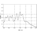
- FIG. 3 is a flowchart illustrating an example of a method for manufacturing an electronic device according to the first embodiment of the present technology. It is an example of sectional drawing of the pixel in a 2nd embodiment of this art. It is a graph which shows an example of the spectral sensitivity characteristic in a 2nd embodiment of this art. It is a graph which shows an example of the spectral sensitivity characteristic at the time of changing the cycle and diameter in a 2nd embodiment of this art.
- First embodiment (example in which the thickness of the surface layer is larger than half the coherence length) 2.
- Second Embodiment Example in which the thickness of the surface layer containing the transparent resin is made larger than half the coherence length) 3.
- Third Embodiment Example in which the thickness of the surface layer including the stress relaxation resin layer is made larger than half of the coherence length
- Fourth Embodiment Example in which the thickness of the surface layer is made larger than half of the coherence length, and a Fabry-Perot resonator is arranged below the coherence length 5).
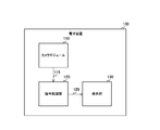
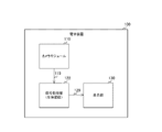
- FIG. 1 is a block diagram illustrating a configuration example of the electronic device 100 according to the first embodiment of the present technology.
- the electronic device 100 is a device for splitting light, and includes a camera module 110, a signal processing unit 120, and a display unit 130.
- a smartphone having a biometric authentication function, a camera mounted on a drone, or the like is assumed.
- the camera module 110 captures image data in synchronization with a vertical scanning signal or the like.
- the camera module 110 supplies image data to the signal processing unit 120 via a signal line 119.
- the signal processing unit 120 performs predetermined signal processing on the image data.
- the signal processing unit 120 obtains a spectral spectrum in signal processing. This spectrum is used for biometric authentication.
- the signal processing unit 120 supplies the processing result to the display unit 130 via the signal line 129.
- the display unit 130 displays the processing result.
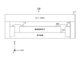
- FIG. 2 is an example of a cross-sectional view of the camera module 110 according to the first embodiment of the present technology.
- the camera module 110 includes a cover glass 111, a solid-state image sensor 200, and a support substrate 113.
- a predetermined direction parallel to the light receiving surface of the cover glass 111 or the solid-state imaging device 200 is defined as an X direction
- a direction perpendicular to the light receiving surface is defined as a Z direction
- a direction perpendicular to the X direction and the Z direction is taken as a Y direction.
- the cross-sectional view of the same figure is a view seen from the Y direction.
- the cover glass 111 protects the light receiving surface of the solid-state imaging device 200.
- a predetermined gas such as air or dry nitrogen gas is filled between the cover glass 111 and the solid-state imaging device 200.
- the solid-state imaging element 200 is connected to the support substrate 113 via the wire 112.
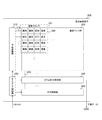
- FIG. 3 is a block diagram illustrating a configuration example of the solid-state imaging device 200 according to the first embodiment of the present technology.
- the solid-state imaging device 200 includes a vertical driving unit 210, a pixel array unit 220, a timing control unit 230, a column signal processing unit 240, and a horizontal driving unit 250.
- a plurality of pixels 300 are arranged in a two-dimensional grid.
- a set of pixels 300 arranged in the horizontal direction is referred to as “row”, and a set of pixels 300 arranged in the direction perpendicular to the row is referred to as “column”.
- the pixel array unit 220 is divided into a plurality of pixel blocks 221 each consisting of a predetermined number of pixels 300.
- each pixel block 221 includes 16 pixels 300 of 4 rows ⁇ 4 columns.
- Each of the pixels 300 in the pixel block 221 receives light having different wavelengths, generates a pixel signal, and supplies the pixel signal to the column signal processing unit 240.
- the timing control unit 230 controls the operation timings of the vertical drive unit 210, the column signal processing unit 240, and the horizontal drive unit 250 in synchronization with the vertical synchronization signal VSYNC.
- the vertical driving unit 210 sequentially drives the rows and outputs pixel signals.
- the column signal processing unit 240 performs AD (Analog-to-Digital) conversion processing, CDS (Correlated Double-Sampling) processing, and the like on the pixel signal from the pixel array unit 220 for each column.
- the column signal processing unit 240 outputs the processed pixel signal to the signal processing unit 120 according to the control of the vertical driving unit 210.
- the horizontal driving unit 250 sequentially selects a column and outputs a pixel signal of the column.
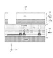
- FIG. 4 is an example of a cross-sectional view of the pixel 300 according to the first embodiment of the present technology.
- a surface layer 310 is disposed on the uppermost layer of the pixel 300 with the direction from the support substrate 113 to the cover glass 111 (in other words, the light receiving side) as the upward direction.
- the surface layer 310 is the first layer in which light is incident through air having a refractive index of 1, and is provided to protect the surface of the solid-state imaging device 200.
- the refractive index of the surface layer 310 is larger than 1, for example.
- a silicon dioxide (SiO 2 ) layer 311 is used as the surface layer 310.
- the filter layer 320 is disposed below the surface layer 310.
- an antireflection film may be further disposed to form the surface layer 310 with a two-layer structure.
- the filter layer 320 transmits predetermined target light out of incident light transmitted through the surface layer 310 and reflects the rest to the surface layer 310.
- the filter layer 320 includes a silicon oxynitride (SiON) layer 321, a silicon nitride (Si 3 N 4 ) layer 322, a silicon oxynitride layer 323, a silicon dioxide layer 324, and a surface plasmon resonance filter 340 in order from the top.
- the refractive indexes of the silicon oxynitride layer 321, the silicon nitride layer 322, and the silicon oxynitride layer 323 are different, and the reflectance of the filter layer 320 can be adjusted by changing the thicknesses of these layers.
- the silicon nitride layer 322 functions as a passivation layer that prevents oxidation of aluminum used for the surface plasmon resonance filter 340.
- the surface plasmon resonance filter 340 transmits light having a predetermined wavelength using a surface plasmon resonance phenomenon in which surface plasmon and light resonate.
- plasmon means a state in which light hits a metal fine particle and the electric electrons inside the metal fine particle are shaken to change the electric field, and free electrons are biased.
- Surface plasmon is a plasmon generated on the metal surface. Point to. Details of the structure of the surface plasmon resonance filter 340 will be described later.
- a silicon dioxide layer 331 is disposed below the filter layer 320.
- a light shielding film 332 is disposed in the vicinity of the outer periphery of the silicon dioxide layer 331. The light shielding film 332 shields light from adjacent pixels and is provided to prevent color mixing.
- An antireflection film 333 is disposed below the silicon dioxide layer 331, and a photoelectric conversion layer 334 is disposed below the antireflection film 333.
- the photoelectric conversion layer 334 photoelectrically converts the target light transmitted through the filter layer 320 to generate a pixel signal.
- a silicon substrate on which a pn junction photodiode is formed is used.
- a wiring layer is further disposed below the photoelectric conversion layer 334, the wiring layer is omitted for convenience of description.
- the cause of the ripple is described. Since the refractive indexes of air and the surface layer 310 are different from each other, when incident light is incident on the surface layer 310, a part of the incident light is transmitted through the light receiving surface p1 of the surface layer 310 and the rest is reflected. A thick solid line in FIG. 4 indicates incident light and reflected light r1 partially reflected.
- the refractive index of each of the surface layer 310 and the filter layer 320 is different, a part of the transmitted light that has passed through the light receiving surface p1 is transmitted through the interface p2 between the surface layer 310 and the filter layer 320, and the rest Is reflected.
- the dashed-dotted line in FIG. 4 shows the transmitted light that has passed through the light receiving surface p1 and the reflected light r2 that is partially reflected.
- the phase difference between the reflected light beams r1 and r2 is determined based on the difference between the optical path lengths of the reflected lights r1 and r2 and the presence or absence of phase inversion due to reflection.
- the phase difference is an integral multiple of the wavelength, it is strengthened, and when it is shifted by half a wavelength, it is weakened. Due to this interference, the reflectance of the pixel 300 varies. Similarly, the transmittance varies.
- the wavelength interval ⁇ when the m (m is an integer) order and the m + 1 order are strengthened is expressed by the following equation.
- ⁇ ⁇ / (4n 1 ) ⁇ (4 ⁇ n + ⁇ / d) Equation 1
- ⁇ represents the wavelength of incident light (natural light or the like), and the unit is, for example, micrometers ( ⁇ m).
- n 1 represents the refractive index of the surface layer 310.
- ⁇ n is a difference in refractive index with respect to the wavelength of the surface layer 310 and indicates refractive index wavelength dispersion.
- d indicates the thickness of the surface layer 310, and the unit is, for example, micrometers ( ⁇ m).
- the interference phenomenon occurs when 2d, which is the optical path difference between the reflected lights r1 and r2, is less than or equal to the coherence length. That is, interference occurs when the following equation is established. 2d ⁇ Lc Formula 2
- Lc is the coherence length of incident light and is represented by the following equation. Lc ⁇ 2 / ⁇
- ⁇ is the spectrum half width, and the unit is, for example, micrometers ( ⁇ m). In natural light, the coherence length Lc is about several micrometers ( ⁇ m).
- the thickness d of the surface layer 310 is set to a value satisfying the following expression from Equation 2, the coherence can be lost. That is, the ripple can be reduced by making the thickness d of the surface layer 310 larger than half of the coherence length Lc. d> Lc / 2 Formula 3
- the ripple can be reduced, but this configuration is not preferable.
- OCL On-Chip micro-Lenses
- the OCL When the OCL is provided, light vertically incident near the center of the lens is directly incident on the surface layer 310 as it is, but light incident on a position shifted from the center is incident on the surface layer 310 in an oblique direction. . At this time, the light incident in the oblique direction changes the optical path length with respect to the vertically incident light, so that the ripple causes a wavelength shift. Therefore, since different lights are incident on one photoelectric conversion layer 334 at the same time, they appear to be integrated to reduce the ripple, and the interference effect itself is not reduced.
- the obliquely incident component causes a demerit that the peak wavelength causes a long wavelength shift and changes to broad spectrum.
- the solid-state imaging device 200 has an OCL-less structure as illustrated in FIG. For this reason, it is possible to narrow the signal processing as compared with the case where the OCL is provided.
- OCL-less means that the uppermost surface layer 310 has no OCL and is flat.
- “Flat” means a state in which there is no unevenness larger than the wavelength of light and it can be regarded as optically flat.
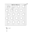
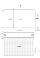
- FIG. 5 is an example of a plan view of the surface plasmon resonance filter 340 according to the first embodiment of the present technology.
- the surface plasmon resonance filter 340 is a thin film made of aluminum (Al) or the like in which a plurality of holes 341 are formed at regular intervals. The interval between adjacent holes 341 is called a “period”. By changing the diameter D of the hole 341 and the period P, the transmission spectrum and its peak wavelength can be adjusted.
- a thin film of gold (Au) or silver (Ag) can be used instead of aluminum.
- a dielectric such as an oxide film may be disposed in the upper or lower layer of the surface plasmon resonance filter 340 or in the hole 341.
- FIG. 6 is a diagram illustrating an example of a diameter and a period for each pixel according to the first embodiment of the present technology. For each pixel 300 in the pixel block 221, at least one of the diameter and period of the surface plasmon resonance filter 340 of the pixel is different.
- x is set to “0” to “3”
- y is set to “0” to “3”.
- the relative coordinates of the pixel 300 are represented by (x, y).
- P0 is set to the period of the pixel 300 having the x coordinate “0”
- P1 is set to the period of the pixel 300 having the x coordinate “1”.
- P2 is set to the period of the pixel 300 having the x coordinate “2”
- P3 is set to the period of the pixel 300 having the x coordinate “3”.
- D0 is set to the diameter of the pixel 300 at the y coordinate “0”
- D1 is set to the diameter of the pixel 300 at the y coordinate “1”.
- D2 is set to the diameter of the pixel 300 at the y coordinate “2”
- D3 is set to the diameter of the pixel 300 at the y coordinate “3”.
- incident light can be split into 16 wavelengths.
- a spectral spectrum is obtained. This spectral spectrum can be used in various applications such as biometric authentication and vegetation survey. If ripples occur in the spectral spectrum, the performance of the application may be degraded. However, by setting the thickness d to satisfy Equation 3, ripples can be reduced and performance degradation can be suppressed.
- the number of pixels in the pixel block 221 is not limited to 16, and may be 9 of 3 ⁇ 3 or 25 of 5 ⁇ 5, for example. If the number of pixels in the pixel block 221 is n (n is an integer), the light can be divided into n wavelength components.
- the spectral sensitivity characteristics when various thicknesses d were set were estimated using a three-dimensional FDTD (Finite-Difference Time-Domain) method.
- FIG. 7 is a graph showing an example of the spectral sensitivity characteristic when the thickness d is 0.1 micrometers ( ⁇ m).
- FIG. 8 is a graph showing an example of spectral sensitivity characteristics when the thickness d is 1.0 micrometer ( ⁇ m).
- FIG. 9 is a graph showing an example of spectral sensitivity characteristics when the thickness d is 1.5 micrometers ( ⁇ m).
- FIG. 10 is a graph showing an example of spectral sensitivity characteristics when the thickness d is 2.0 micrometers ( ⁇ m).
- FIG. 11 is a graph showing an example of the spectral sensitivity characteristic when the thickness d is 2.5 micrometers ( ⁇ m). 7 to 11, the vertical axis indicates the spectral sensitivity, and the horizontal axis indicates the wavelength.
- FIG. 12 is a graph showing the measurement result of the spectral amplitude in the first embodiment of the present technology.
- the vertical axis indicates the spectral amplitude obtained from FIGS. 7 to 11, and the horizontal axis indicates the thickness d.
- This spectral amplitude represents the magnitude of the ripple.
- the thickness d is less than 2.0 micrometers ( ⁇ m)
- the thinner the thickness d the smaller the spectral amplitude (ripple) and the greater the reduction effect.
- the thickness d is 2.0 micrometers ( ⁇ m) or more
- the spectral amplitude is saturated.
- incident light is natural light, d is preferably 2.0 micrometers ( ⁇ m) or more.
- the solid-state image sensor 200 is formed on the support substrate 113 by the manufacturing system of the electronic device 100.
- FIG. 13 is an example of a cross-sectional view of the electronic device 100 in which the solid-state imaging element 200 according to the first embodiment of the present technology is formed.
- the surface layer 310 to the photoelectric conversion layer 334 are provided in order from the top, and the wiring layer 410 is provided below the photoelectric conversion layer 334.
- the wiring layer 410 is provided with a pad 411.
- a resist that is partially opened is applied to the surface layer 310 of the solid-state imaging device 200.
- FIG. 14 is an example of a cross-sectional view of the electronic device 100 coated with a resist according to the first embodiment of the present technology.
- a resist 501 is opened at the connection portion of the pad 411.
- an initial etch is performed using lithographic techniques. In lithography, mask exposure and development are sequentially performed. Then, the resist 501 is removed. Etching may be either dry etching or wet etching.
- FIG. 15 is an example of a cross-sectional view of the electronic device 100 that has performed the first etching according to the first embodiment of the present technology.
- the first etching part of the surface layer 310 and the filter layer 320 are opened, and the photoelectric conversion layer 334 in the part is exposed.
- a resist is applied again to the solid-state imaging device 200.
- FIG. 16 is an example of a cross-sectional view of the electronic device 100 in which a resist 502 is applied after etching according to the first embodiment of the present technology.
- a part of the resist 502 is opened, and the area of the part is narrower than the opening part of the resist 501 in the first etching. Thereby, damage to the solid-state imaging device 200 during the second etching can be reduced.
- a second etching is performed using a lithography technique. Then, the resist 502 is removed.
- FIG. 17 is an example of a cross-sectional view of the electronic device 100 that has been subjected to the second etching according to the first embodiment of the present technology.
- the second etching a part of the photoelectric conversion layer 334 and the wiring layer 410 is opened, and the connection portion of the pad 411 is exposed.
- This connection location is connected to the electrode of the support substrate 113 by wire bonding.
- the solid-state imaging device 200 and the support substrate 113 are electrically connected.
- various processes are executed to complete the electronic device 100.
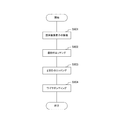
- FIG. 18 is a flowchart illustrating an example of a method for manufacturing the electronic device 100 according to the first embodiment of the present technology.
- the manufacturing system manufactures the solid-state imaging device 200 on the support substrate 113 (step S901), and performs the first etching (step S902). Then, the manufacturing system performs the second etching (step S903), and electrically connects the solid-state imaging device 200 and the support substrate 113 by wire bonding (step S904). After step S904, the manufacturing system executes various processes and ends the manufacturing of the electronic device 100.
- the thickness of the surface layer 310 is larger than half of the coherence length, the reflected light reflected by the light receiving surface of the surface layer 310 and the interface below the reflected light. Interference with reflected reflected light can be suppressed. Thereby, the ripple in a spectral spectrum can be reduced.
- the silicon dioxide layer 311 is used as the surface layer 310.
- the silicon wafer may be warped during heat treatment due to the difference in thermal expansion coefficient between them.
- the warpage of the silicon wafer may increase.
- the solid-state imaging device 200 of the second embodiment is different from the first embodiment in that a transparent resin layer is provided instead of the silicon dioxide layer 311.
- FIG. 19 is an example of a cross-sectional view of the pixel 300 according to the second embodiment of the present technology.
- the pixel 300 according to the second embodiment differs from the first embodiment in that an antireflection film 312 and a transparent resin layer 313 are arranged in order from the top instead of the silicon dioxide layer 311 in the surface layer 310. .
- the thickness d of the surface layer 310 shall satisfy Formula 3 as in the first embodiment.
- the antireflection film 312 is a film for reducing the reflectance of the surface layer 310, and silicon dioxide (SiO 2 ) or the like is used. This antireflection film 312 is much thinner than the transparent resin layer 313. Note that the antireflection film 312 may not be formed.
- the transparent resin layer 313 for example, a resin having a difference in coefficient of thermal expansion from that of a silicon wafer is smaller than that of silicon dioxide. By using such a resin, warpage of the silicon wafer due to heat treatment can be suppressed.
- the transparent resin layer 313 is formed by, for example, a spin coating method. By using the spin coating method, the surface layer 310 can be formed at a higher speed than when the silicon dioxide layer 311 is formed.
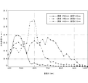
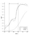
- FIG. 20 is a graph illustrating an example of spectral sensitivity characteristics according to the second embodiment of the present technology.
- the vertical axis indicates spectral sensitivity
- the horizontal axis indicates wavelength.
- the thickness d was set to 3.0 micrometers ( ⁇ m), which is a value satisfying Equation 3, and was obtained by simulation using the FDTD method.
- 3.0 micrometers (micrometer) is the thickness of the grade which can be produced
- the solid line in the figure shows the spectral sensitivity characteristics when the thickness d is 3.0 micrometers ( ⁇ m).
- the same simulation was performed with the thickness d set to 0.4 ⁇ m, which does not satisfy Equation 3.
- the dotted line in the figure shows the spectral sensitivity characteristics of the comparative example.
- the amplitude (ripple) can be made smaller than that of the comparative example not satisfying Expression 3 by setting the thickness to satisfy Expression 3.
- FIG. 21 is a graph showing an example of spectral sensitivity characteristics when the period and diameter are changed in the second embodiment of the present technology.
- the vertical axis indicates the spectral sensitivity
- the horizontal axis indicates the wavelength.
- the solid line indicates the spectral sensitivity characteristics of the pixel in which the period of the surface plasmon resonance filter 340 is 250 nanometers (nm) and the diameter is 140 nanometers (nm).
- a one-dot chain line indicates a spectral sensitivity characteristic of a pixel in which the period of the surface plasmon resonance filter 340 is 350 nanometers (nm) and the diameter is 210 nanometers (nm).
- a dotted line indicates the spectral sensitivity characteristic of a pixel in which the period of the surface plasmon resonance filter 340 is 450 nanometers (nm) and the diameter is 270 nanometers (nm). As illustrated in the figure, different spectral sensitivity characteristics can be obtained by changing at least one of the period and the diameter.
- the transparent resin layer 313 whose thermal expansion coefficient difference from the silicon wafer is smaller than that of silicon dioxide is disposed as the surface layer having a thickness larger than half of the coherence length. Therefore, warpage of the silicon wafer due to heat treatment can be suppressed.
- the transparent resin layer 313 is formed on the silicon oxynitride layer 321. However, in this configuration, the transparent resin layer 313 may be peeled off when dicing is performed.
- the solid-state imaging device 200 of the third embodiment is different from the second embodiment in that a stress relaxation resin layer is formed in order to improve the adhesion of the transparent resin layer 313.
- FIG. 22 is an example of a cross-sectional view of the pixel 300 according to the third embodiment of the present technology.
- the pixel 300 according to the third embodiment differs from the second embodiment in that a stress relaxation resin layer 314 is further formed below the transparent resin layer 313 in the surface layer 310.
- the stress relaxation resin layer 314 is a layer that relieves stress applied to the transparent resin layer 313. Further, the thickness of the surface layer 310 including the stress relaxation resin layer 314 satisfies the expression 3 as in the first embodiment.
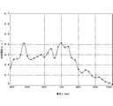
- FIG. 23 is a graph illustrating an example of spectral sensitivity characteristics according to the third embodiment of the present technology.
- the vertical axis indicates the spectral sensitivity
- the horizontal axis indicates the wavelength.
- the solid line in the figure shows the spectral sensitivity characteristics of the pixel 300 of the third embodiment having the stress relaxation resin layer 314.
- the dotted line in the figure shows the spectral sensitivity characteristics of the pixel 300 of the second embodiment that does not have the stress relaxation resin layer 314.
- the absence of the stress relaxation resin layer 314 is considered to reduce the ripple because the number of interfaces is smaller.
- the spectral sensitivity actually depends on the presence or absence of the stress relaxation resin layer 314. There is no significant difference in characteristics. Therefore, the formation of the stress relaxation resin layer 314 does not increase the ripple.
- the stress relaxation resin layer 314 since the stress relaxation resin layer 314 is further formed, the stress applied to the transparent resin layer 313 can be relaxed to prevent the transparent resin layer 313 from peeling off. it can.
- a desired wavelength is transmitted by the surface plasmon resonance filter 340 in which fine holes 341 are formed.
- the solid-state imaging device 200 according to the fourth embodiment differs from the first embodiment in that a Fabry-Perot resonator that does not require a hole is used instead of the surface plasmon resonance filter 340.
- FIG. 24 is an example of a cross-sectional view of the pixel 300 according to the fourth embodiment of the present technology.
- the pixel 300 according to the fourth embodiment is the first embodiment in that a Fabry-Perot resonator 350 is arranged in the filter layer 320 instead of the layers from the silicon oxynitride layer 321 to the surface plasmon resonance filter 340.
- the form is different.
- the Fabry-Perot resonator 350 transmits two light beams having a predetermined wavelength by using two half mirrors facing each other and utilizing resonance between light reflected in a multiple manner between the half mirrors. is there. These half mirrors do not have holes and do not require fine processing such as a surface plasmon resonance filter.
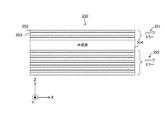
- FIG. 25 is an example of a cross-sectional view of a Fabry-Perot resonator 350 according to the fourth embodiment of the present technology.
- the Fabry-Perot resonator 350 includes a half mirror 351, a resonator 354, and a half mirror 355 in order from the top.
- the half mirror 351 transmits a part of incident light and reflects the rest, and is constituted by a multilayer film in which titanium oxide (TiO 2 ) layers 352 and silicon dioxide layers 353 are alternately arranged. The same applies to the half mirror 355.
- the multilayer film is used as the half mirrors 351 and 355, other than the multilayer film such as a metal thin film can be used as the half mirror as long as a part of the multilayer film can be reflected.
- the resonator 354 is formed of, for example, a silicon dioxide layer. By changing the thickness of the resonator 354, the wavelength to be transmitted can be adjusted. In the pixel block 221, the thicknesses of the resonators 354 of the 16 pixels 300 are different. Thereby, incident light can be split into 16 wavelengths.
- the transparent resin layer 313 may be disposed as the surface layer 310 as in the second embodiment. Further, a stress relaxation resin layer 314 may be further disposed as in the third embodiment.
- the Fabry-Perot resonator 350 is disposed as the filter layer 320, compared with the configuration in which the surface plasmon resonance filter 340 is disposed, microfabrication is not required, and the manufacturing is performed. Becomes easier.
- the electronic device 100 performs only the spectroscopy of incident light. However, when investigating the plant growth state (ie, vegetation), it is desirable to calculate a normalized vegetation index (NDVI) after spectroscopy.
- NDVI is a numerical value indicating the state of vegetation, and the more positive NDVI is, the darker the vegetation is.
- the solid-state imaging device 200 according to the fifth embodiment is different from the first embodiment in that NDVI is calculated.
- FIG. 26 is a block diagram illustrating a configuration example of the electronic device 100 according to the fifth embodiment of the present technology.
- the electronic device 100 of the fifth embodiment is different from the first embodiment in that it further includes a solid-state imaging device 201 and a signal processing unit 121 instead of the signal processing unit 120.
- a camera mounted on a drone such as a small unmanned helicopter is assumed.
- the solid-state imaging device 200 splits visible light and supplies image data to the signal processing unit 121.
- the solid-state imaging device 201 separates invisible light such as infrared light and supplies image data to the signal processing unit 121.
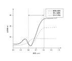
- FIG. 27 is a graph illustrating an example of the reflectance for each wavelength according to the fifth embodiment of the present technology.
- the vertical axis indicates the reflectance of a subject (such as a plant), and the horizontal axis indicates the wavelength.
- the solid line shows the reflectance characteristics of healthy plants, and the alternate long and short dash line shows the reflectance characteristics of weak plants.
- the dotted line indicates the reflectance characteristics of withered plants.
- the difference in reflectance for each state of the plant becomes large. Further, the difference is further increased in the infrared light region longer than 0.8 micrometers ( ⁇ m).
- the vegetation state can be determined by detecting the signal levels of the visible light region and the infrared light region by the solid-state imaging devices 200 and 201. Then, by placing such an electronic device 100 on a drone and observing the growing state (vegetation) of the crop from above, the user can efficiently grow the crop.
- the transparent resin layer 313 may be disposed as the surface layer 310 as in the second embodiment. Further, a stress relaxation resin 314 may be further arranged as in the third embodiment. Further, a Fabry-Perot resonator 350 may be arranged as in the fourth embodiment.
- the electronic apparatus 100 obtains the normalized vegetation index (NDVI) by obtaining the reflectance of the subject with respect to visible light and the reflectance of the subject with respect to invisible light. Can be calculated.
- NDVI normalized vegetation index
- the electronic device 100 performs only the spectroscopy of incident light. However, when using the electronic device 100 for biometric authentication, it is desirable to further determine whether the skin is human skin by analyzing the spectral spectrum.
- the electronic device 100 according to the sixth embodiment is different from the first embodiment in that biometric authentication is performed using a spectral spectrum.
- FIG. 28 is a block diagram illustrating a configuration example of the electronic device 100 according to the sixth embodiment of the present technology.
- the electronic device 100 according to the sixth embodiment is different from the first embodiment in that a signal processing unit 122 is provided instead of the signal processing unit 120.
- a signal processing unit 122 is provided instead of the signal processing unit 120.
- an apparatus or a device such as a smartphone having a biometric authentication function is assumed.
- the signal processing unit 122 performs biometric authentication.
- biometric authentication the signal processing unit 122 analyzes the spectral spectrum and determines whether the subject is human skin.
- matching is performed between the biological pattern (face, fingerprint, iris, etc.) of the subject and a registered pattern registered in advance, and the result is supplied to the display unit 130. In this way, by determining whether or not the subject is human skin using the spectral spectrum, the authentication accuracy can be improved as compared with the case where this determination is not performed.
- FIG. 29 is a graph illustrating an example of the reflectance for each wavelength according to the sixth embodiment of the present technology.
- the vertical axis in the figure is the reflectance of the subject, and the horizontal axis is the wavelength.
- the solid line in the figure shows the reflectance characteristics of the Mongoloid skin, and the dotted line shows the reflectance characteristics of the Caucasian skin.
- the alternate long and short dash line indicates the reflectance characteristics of the negroid skin.
- the reflectance varies greatly in the wavelength region of 450 to 650 nanometers (nm). For this reason, for example, the signal processing unit 122 can determine whether or not the subject is human skin by analyzing the spectral spectrum in this wavelength region.
- the transparent resin layer 313 may be disposed as the surface layer 310 as in the second embodiment. Further, a stress relaxation resin 314 may be further arranged as in the third embodiment. Further, a Fabry-Perot resonator 350 may be arranged as in the fourth embodiment.
- the electronic device 100 determines whether the skin is human skin using the spectral spectrum in the biometric authentication.
- the accuracy of authentication can be improved.
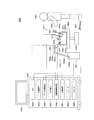
- FIG. 30 is a diagram illustrating an example of a schematic configuration of an endoscopic surgery system 5000 to which the technology according to the present disclosure can be applied.
- FIG. 30 shows a state where an operator (doctor) 5067 is performing surgery on a patient 5071 on a patient bed 5069 using an endoscopic surgery system 5000.
- an endoscopic surgery system 5000 includes an endoscope 5001, other surgical tools 5017, a support arm device 5027 that supports the endoscope 5001, and various devices for endoscopic surgery. And a cart 5037 on which is mounted.
- trocars 5025a to 5025d are punctured into the abdominal wall.
- the lens barrel 5003 of the endoscope 5001 and other surgical tools 5017 are inserted into the body cavity of the patient 5071 from the trocars 5025a to 5025d.
- an insufflation tube 5019, an energy treatment tool 5021, and forceps 5023 are inserted into the body cavity of the patient 5071.
- the energy treatment device 5021 is a treatment device that performs tissue incision and separation, blood vessel sealing, or the like by high-frequency current or ultrasonic vibration.
- the illustrated surgical tool 5017 is merely an example, and as the surgical tool 5017, for example, various surgical tools generally used in endoscopic surgery such as a lever and a retractor may be used.
- the image of the surgical site in the body cavity of the patient 5071 captured by the endoscope 5001 is displayed on the display device 5041.
- the surgeon 5067 performs a treatment such as excision of the affected part, for example, using the energy treatment tool 5021 and the forceps 5023 while viewing the image of the surgical part displayed on the display device 5041 in real time.
- the pneumoperitoneum tube 5019, the energy treatment tool 5021, and the forceps 5023 are supported by an operator 5067 or an assistant during surgery.
- the support arm device 5027 includes an arm portion 5031 extending from the base portion 5029.
- the arm portion 5031 includes joint portions 5033a, 5033b, and 5033c and links 5035a and 5035b, and is driven by control from the arm control device 5045.
- the endoscope 5001 is supported by the arm unit 5031, and the position and posture thereof are controlled. Thereby, the stable position fixing of the endoscope 5001 can be realized.
- the endoscope 5001 includes a lens barrel 5003 in which a region having a predetermined length from the distal end is inserted into the body cavity of the patient 5071, and a camera head 5005 connected to the proximal end of the lens barrel 5003.
- a lens barrel 5003 in which a region having a predetermined length from the distal end is inserted into the body cavity of the patient 5071, and a camera head 5005 connected to the proximal end of the lens barrel 5003.
- an endoscope 5001 configured as a so-called rigid mirror having a rigid lens barrel 5003 is illustrated, but the endoscope 5001 is configured as a so-called flexible mirror having a flexible lens barrel 5003. Also good.
- An opening into which an objective lens is fitted is provided at the tip of the lens barrel 5003.
- a light source device 5043 is connected to the endoscope 5001, and light generated by the light source device 5043 is guided to the tip of the lens barrel by a light guide extending inside the lens barrel 5003. Irradiation is performed toward the observation target in the body cavity of the patient 5071 through the lens.
- the endoscope 5001 may be a direct endoscope, a perspective mirror, or a side endoscope.
- An optical system and an image sensor are provided inside the camera head 5005, and reflected light (observation light) from the observation target is condensed on the image sensor by the optical system. Observation light is photoelectrically converted by the imaging element, and an electrical signal corresponding to the observation light, that is, an image signal corresponding to the observation image is generated.
- the image signal is transmitted to a camera control unit (CCU) 5039 as RAW data.
- CCU camera control unit
- the camera head 5005 is equipped with a function of adjusting the magnification and the focal length by appropriately driving the optical system.
- a plurality of imaging elements may be provided in the camera head 5005 in order to cope with, for example, stereoscopic viewing (3D display).
- a plurality of relay optical systems are provided inside the lens barrel 5003 in order to guide observation light to each of the plurality of imaging elements.
- the CCU 5039 is configured by a CPU (Central Processing Unit), a GPU (Graphics Processing Unit), and the like, and comprehensively controls operations of the endoscope 5001 and the display device 5041. Specifically, the CCU 5039 performs various types of image processing for displaying an image based on the image signal, such as development processing (demosaic processing), for example, on the image signal received from the camera head 5005. The CCU 5039 provides the display device 5041 with the image signal subjected to the image processing. Further, the CCU 5039 transmits a control signal to the camera head 5005 to control the driving thereof.
- the control signal can include information regarding imaging conditions such as magnification and focal length.
- the display device 5041 displays an image based on an image signal subjected to image processing by the CCU 5039 under the control of the CCU 5039.
- the endoscope 5001 is compatible with high-resolution imaging such as 4K (horizontal pixel number 3840 ⁇ vertical pixel number 2160) or 8K (horizontal pixel number 7680 ⁇ vertical pixel number 4320), and / or 3D display
- the display device 5041 may be a display device capable of high-resolution display and / or 3D display.
- 4K or 8K high-resolution imaging a more immersive feeling can be obtained by using a display device 5041 having a size of 55 inches or more.
- a plurality of display devices 5041 having different resolutions and sizes may be provided depending on applications.
- the light source device 5043 is composed of a light source such as an LED (light emitting diode), for example, and supplies irradiation light to the endoscope 5001 when photographing a surgical site.
- a light source such as an LED (light emitting diode)
- the arm control device 5045 is configured by a processor such as a CPU, for example, and operates according to a predetermined program to control driving of the arm portion 5031 of the support arm device 5027 according to a predetermined control method.
- the input device 5047 is an input interface for the endoscopic surgery system 5000.
- the user can input various information and instructions to the endoscopic surgery system 5000 via the input device 5047.
- the user inputs various types of information related to the operation, such as the patient's physical information and information about the surgical technique, via the input device 5047.
- the user instructs the arm unit 5031 to be driven via the input device 5047 or the instruction to change the imaging conditions (type of irradiation light, magnification, focal length, etc.) by the endoscope 5001. Then, an instruction to drive the energy treatment instrument 5021 is input.
- the type of the input device 5047 is not limited, and the input device 5047 may be various known input devices.
- the input device 5047 for example, a mouse, a keyboard, a touch panel, a switch, a foot switch 5057, and / or a lever can be applied.
- the touch panel may be provided on the display surface of the display device 5041.
- the input device 5047 is a device worn by the user, such as a glasses-type wearable device or an HMD (Head Mounted Display), and various types of input are performed according to the user's gesture and line of sight detected by these devices. Is done.
- the input device 5047 includes a camera capable of detecting the user's movement, and various inputs are performed according to the user's gesture and line of sight detected from the video captured by the camera.
- the input device 5047 includes a microphone that can pick up a user's voice, and various inputs are performed by voice through the microphone.
- the input device 5047 is configured to be able to input various information without contact, so that a user belonging to a clean area (for example, an operator 5067) can operate a device belonging to an unclean area without contact. Is possible.
- a user belonging to a clean area for example, an operator 5067
- the user can operate the device without releasing his / her hand from the surgical tool he / she has, the convenience for the user is improved.
- the treatment instrument control device 5049 controls the drive of the energy treatment instrument 5021 for tissue cauterization, incision, or blood vessel sealing.
- the pneumoperitoneum device 5051 gas is introduced into the body cavity via the pneumoperitoneum tube 5019.
- the recorder 5053 is an apparatus capable of recording various types of information related to surgery.
- the printer 5055 is a device that can print various types of information related to surgery in various formats such as text, images, or graphs.
- the support arm device 5027 includes a base portion 5029 as a base and an arm portion 5031 extending from the base portion 5029.
- the arm portion 5031 includes a plurality of joint portions 5033a, 5033b, and 5033c and a plurality of links 5035a and 5035b connected by the joint portion 5033b.
- FIG. The configuration of the arm portion 5031 is shown in a simplified manner. Actually, the shape, number and arrangement of the joint portions 5033a to 5033c and the links 5035a and 5035b, the direction of the rotation axis of the joint portions 5033a to 5033c, etc. are appropriately set so that the arm portion 5031 has a desired degree of freedom. obtain.
- the arm portion 5031 can be preferably configured to have 6 degrees of freedom or more. Accordingly, the endoscope 5001 can be freely moved within the movable range of the arm portion 5031. Therefore, the barrel 5003 of the endoscope 5001 can be inserted into the body cavity of the patient 5071 from a desired direction. It becomes possible.
- the joint portions 5033a to 5033c are provided with actuators, and the joint portions 5033a to 5033c are configured to be rotatable around a predetermined rotation axis by driving the actuators.
- the arm control device 5045 By controlling the driving of the actuator by the arm control device 5045, the rotation angles of the joint portions 5033a to 5033c are controlled, and the driving of the arm portion 5031 is controlled. Thereby, control of the position and orientation of the endoscope 5001 can be realized.
- the arm control device 5045 can control the driving of the arm unit 5031 by various known control methods such as force control or position control.
- the arm control device 5045 appropriately controls the driving of the arm unit 5031 according to the operation input.
- the position and posture of the endoscope 5001 may be controlled.
- the endoscope 5001 at the tip of the arm portion 5031 can be moved from an arbitrary position to an arbitrary position, and then fixedly supported at the position after the movement.
- the arm portion 5031 may be operated by a so-called master slave method.
- the arm unit 5031 can be remotely operated by the user via the input device 5047 installed at a location away from the operating room.
- the arm control device 5045 When force control is applied, the arm control device 5045 receives the external force from the user and moves the actuators of the joint portions 5033a to 5033c so that the arm portion 5031 moves smoothly according to the external force. You may perform what is called power assist control to drive. Accordingly, when the user moves the arm unit 5031 while directly touching the arm unit 5031, the arm unit 5031 can be moved with a relatively light force. Therefore, the endoscope 5001 can be moved more intuitively and with a simpler operation, and user convenience can be improved.
- an endoscope 5001 is supported by a doctor called a scopist.
- the position of the endoscope 5001 can be more reliably fixed without relying on human hands, so that an image of the surgical site can be stably obtained. It becomes possible to perform the operation smoothly.
- the arm control device 5045 is not necessarily provided in the cart 5037. Further, the arm control device 5045 is not necessarily a single device. For example, the arm control device 5045 may be provided in each joint portion 5033a to 5033c of the arm portion 5031 of the support arm device 5027, and the plurality of arm control devices 5045 cooperate with each other to drive the arm portion 5031. Control may be realized.
- the light source device 5043 supplies irradiation light to the endoscope 5001 when photographing a surgical site.
- the light source device 5043 is composed of a white light source composed of, for example, an LED, a laser light source, or a combination thereof.
- a white light source is configured by a combination of RGB laser light sources, the output intensity and output timing of each color (each wavelength) can be controlled with high accuracy. Adjustments can be made.
- each RGB light source is controlled by irradiating the observation target with laser light from each of the RGB laser light sources in a time-sharing manner and controlling the driving of the image sensor of the camera head 5005 in synchronization with the irradiation timing. It is also possible to take the images that have been taken in time division. According to this method, a color image can be obtained without providing a color filter in the image sensor.
- the driving of the light source device 5043 may be controlled so as to change the intensity of the output light every predetermined time.
- the driving of the image sensor of the camera head 5005 is controlled to acquire images in a time-sharing manner, and the images are synthesized, so that high dynamics without so-called blackout and overexposure are obtained. A range image can be generated.
- the light source device 5043 may be configured to be able to supply light of a predetermined wavelength band corresponding to special light observation.
- special light observation for example, by utilizing the wavelength dependence of light absorption in body tissue, the surface of the mucous membrane is irradiated by irradiating light in a narrow band compared to irradiation light (ie, white light) during normal observation.
- narrow band imaging is performed in which a predetermined tissue such as a blood vessel is imaged with high contrast.
- fluorescence observation may be performed in which an image is obtained by fluorescence generated by irradiating excitation light.
- the body tissue is irradiated with excitation light to observe fluorescence from the body tissue (autofluorescence observation), or a reagent such as indocyanine green (ICG) is locally administered to the body tissue and applied to the body tissue.
- a reagent such as indocyanine green (ICG) is locally administered to the body tissue and applied to the body tissue.
- ICG indocyanine green
- the light source device 5043 can be configured to be able to supply narrowband light and / or excitation light corresponding to such special light observation.
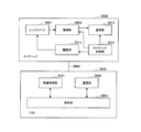
- FIG. 31 is a block diagram showing an example of the functional configuration of the camera head 5005 and CCU 5039 shown in FIG.
- the camera head 5005 includes a lens unit 5007, an imaging unit 5009, a drive unit 5011, a communication unit 5013, and a camera head control unit 5015 as its functions.
- the CCU 5039 includes a communication unit 5059, an image processing unit 5061, and a control unit 5063 as its functions.
- the camera head 5005 and the CCU 5039 are connected to each other via a transmission cable 5065 so that they can communicate with each other.
- the lens unit 5007 is an optical system provided at a connection portion with the lens barrel 5003. Observation light captured from the tip of the lens barrel 5003 is guided to the camera head 5005 and enters the lens unit 5007.
- the lens unit 5007 is configured by combining a plurality of lenses including a zoom lens and a focus lens. The optical characteristics of the lens unit 5007 are adjusted so that the observation light is condensed on the light receiving surface of the image sensor of the imaging unit 5009. Further, the zoom lens and the focus lens are configured such that their positions on the optical axis are movable in order to adjust the magnification and focus of the captured image.
- the imaging unit 5009 is configured by an imaging element, and is disposed in the subsequent stage of the lens unit 5007.
- the observation light that has passed through the lens unit 5007 is collected on the light receiving surface of the image sensor, and an image signal corresponding to the observation image is generated by photoelectric conversion.
- the image signal generated by the imaging unit 5009 is provided to the communication unit 5013.
- CMOS Complementary Metal Oxide Semiconductor
- the imaging element for example, an element capable of capturing a high-resolution image of 4K or more may be used.
- the image sensor that configures the image capturing unit 5009 is configured to include a pair of image sensors for acquiring right-eye and left-eye image signals corresponding to 3D display. By performing the 3D display, the operator 5067 can more accurately grasp the depth of the living tissue in the surgical site.
- the imaging unit 5009 is configured as a multi-plate type, a plurality of lens units 5007 are also provided corresponding to each imaging element.
- the imaging unit 5009 is not necessarily provided in the camera head 5005.
- the imaging unit 5009 may be provided inside the lens barrel 5003 immediately after the objective lens.
- the driving unit 5011 includes an actuator, and moves the zoom lens and the focus lens of the lens unit 5007 by a predetermined distance along the optical axis under the control of the camera head control unit 5015. Thereby, the magnification and focus of the image captured by the imaging unit 5009 can be adjusted as appropriate.
- the communication unit 5013 is configured by a communication device for transmitting and receiving various types of information to and from the CCU 5039.
- the communication unit 5013 transmits the image signal obtained from the imaging unit 5009 as RAW data to the CCU 5039 via the transmission cable 5065.
- the image signal is preferably transmitted by optical communication.
- the surgeon 5067 performs the surgery while observing the state of the affected area with the captured image, so that a moving image of the surgical site is displayed in real time as much as possible for safer and more reliable surgery. Because it is required.
- the communication unit 5013 is provided with a photoelectric conversion module that converts an electrical signal into an optical signal.
- the image signal is converted into an optical signal by the photoelectric conversion module, and then transmitted to the CCU 5039 via the transmission cable 5065.
- the communication unit 5013 receives a control signal for controlling driving of the camera head 5005 from the CCU 5039.
- the control signal includes, for example, information for designating the frame rate of the captured image, information for designating the exposure value at the time of imaging, and / or information for designating the magnification and focus of the captured image. Contains information about the condition.
- the communication unit 5013 provides the received control signal to the camera head control unit 5015.
- the control signal from the CCU 5039 may also be transmitted by optical communication.
- the communication unit 5013 is provided with a photoelectric conversion module that converts an optical signal into an electric signal.
- the control signal is converted into an electric signal by the photoelectric conversion module, and then provided to the camera head control unit 5015.
- the imaging conditions such as the frame rate, exposure value, magnification, and focus are automatically set by the control unit 5063 of the CCU 5039 based on the acquired image signal. That is, a so-called AE (Auto Exposure) function, AF (Auto Focus) function, and AWB (Auto White Balance) function are mounted on the endoscope 5001.
- AE Auto Exposure
- AF Automatic Focus
- AWB Automatic White Balance
- the camera head control unit 5015 controls driving of the camera head 5005 based on a control signal from the CCU 5039 received via the communication unit 5013. For example, the camera head control unit 5015 controls driving of the imaging element of the imaging unit 5009 based on information indicating that the frame rate of the captured image is specified and / or information indicating that the exposure at the time of imaging is specified. For example, the camera head control unit 5015 appropriately moves the zoom lens and the focus lens of the lens unit 5007 via the drive unit 5011 based on information indicating that the magnification and focus of the captured image are designated.
- the camera head control unit 5015 may further have a function of storing information for identifying the lens barrel 5003 and the camera head 5005.
- the camera head 5005 can be resistant to autoclave sterilization by arranging the lens unit 5007, the imaging unit 5009, and the like in a sealed structure with high airtightness and waterproofness.
- the communication unit 5059 is configured by a communication device for transmitting and receiving various types of information to and from the camera head 5005.
- the communication unit 5059 receives an image signal transmitted from the camera head 5005 via the transmission cable 5065.
- the image signal can be suitably transmitted by optical communication.
- the communication unit 5059 is provided with a photoelectric conversion module that converts an optical signal into an electric signal.
- the communication unit 5059 provides the image processing unit 5061 with the image signal converted into the electrical signal.
- the communication unit 5059 transmits a control signal for controlling the driving of the camera head 5005 to the camera head 5005.
- the control signal may also be transmitted by optical communication.
- the image processing unit 5061 performs various types of image processing on the image signal that is RAW data transmitted from the camera head 5005. Examples of the image processing include development processing, high image quality processing (band enhancement processing, super-resolution processing, NR (Noise reduction) processing and / or camera shake correction processing, etc.), and / or enlargement processing (electronic zoom processing). Various known signal processing is included.
- the image processing unit 5061 performs detection processing on the image signal for performing AE, AF, and AWB.
- the image processing unit 5061 is configured by a processor such as a CPU or a GPU, and the above-described image processing and detection processing can be performed by the processor operating according to a predetermined program.
- the image processing unit 5061 is configured by a plurality of GPUs, the image processing unit 5061 appropriately divides information related to the image signal, and performs image processing in parallel by the plurality of GPUs.
- the control unit 5063 performs various controls relating to imaging of the surgical site by the endoscope 5001 and display of the captured image. For example, the control unit 5063 generates a control signal for controlling driving of the camera head 5005. At this time, when the imaging condition is input by the user, the control unit 5063 generates a control signal based on the input by the user. Alternatively, when the endoscope 5001 is equipped with the AE function, the AF function, and the AWB function, the control unit 5063 determines the optimum exposure value, focal length, and the like according to the detection processing result by the image processing unit 5061. A white balance is appropriately calculated and a control signal is generated.
- control unit 5063 causes the display device 5041 to display an image of the surgical site based on the image signal subjected to the image processing by the image processing unit 5061.
- the control unit 5063 recognizes various objects in the surgical unit image using various image recognition techniques. For example, the control unit 5063 detects the shape and color of the edge of the object included in the surgical part image, thereby removing surgical tools such as forceps, specific biological parts, bleeding, mist when using the energy treatment tool 5021, and the like. Can be recognized.
- the control unit 5063 displays various types of surgery support information on the image of the surgical site using the recognition result. Surgery support information is displayed in a superimposed manner and presented to the operator 5067, so that the surgery can be performed more safely and reliably.
- the transmission cable 5065 for connecting the camera head 5005 and the CCU 5039 is an electric signal cable corresponding to electric signal communication, an optical fiber corresponding to optical communication, or a composite cable thereof.
- communication is performed by wire using the transmission cable 5065, but communication between the camera head 5005 and the CCU 5039 may be performed wirelessly.
- communication between the two is performed wirelessly, there is no need to install the transmission cable 5065 in the operating room, so that the situation where the movement of the medical staff in the operating room is hindered by the transmission cable 5065 can be eliminated.
- the endoscopic surgery system 5000 to which the technology according to the present disclosure can be applied has been described.
- the endoscopic surgery system 5000 has been described as an example, but a system to which the technology according to the present disclosure can be applied is not limited to such an example.
- the technology according to the present disclosure may be applied to a testing flexible endoscope system or a microscope operation system.
- the technology according to the present disclosure can be suitably applied to the imaging unit 5009 and the image processing unit 5061 among the configurations described above.
- the solid-state imaging device 200 in FIG. 2 can be applied to the imaging unit 5009 and the signal processing unit 120 in FIG. 1 can be applied to the image processing unit 5061.
- this technique can also take the following structures.
- a surface layer having a thickness exceeding half the coherence length of incident light A filter layer that transmits predetermined target light out of the incident light transmitted through the surface layer and reflects the remainder to the surface layer;
- a solid-state imaging device comprising: a photoelectric conversion layer that photoelectrically converts the predetermined target light transmitted through the filter layer.
- the surface layer further includes a silicon dioxide layer.
- the surface layer further includes a transparent resin layer.
- the filter layer includes a surface plasmon resonance filter.
- the incident light includes natural light,
- the thickness of the said surface layer is a solid-state image sensor in any one of said (1) to (7) which is not less than 2.0 micrometers.
- a surface layer having a thickness exceeding half the coherence length of the incident light A filter layer that transmits predetermined target light out of the incident light transmitted through the surface layer and reflects the remainder to the surface layer; A photoelectric conversion layer that photoelectrically converts the predetermined target light transmitted through the filter layer to generate a pixel signal; and
- An electronic apparatus comprising: a signal processing unit that performs predetermined signal processing on the pixel signal. (10) further comprising a cover glass; The electronic device according to (9), wherein the incident light is incident on the surface layer through the cover glass and a predetermined gas. (11) The electronic device according to (9) or (10), wherein the signal processing unit obtains a normalized vegetation index in the signal processing.
Landscapes
- Physics & Mathematics (AREA)
- Engineering & Computer Science (AREA)
- General Physics & Mathematics (AREA)
- Optics & Photonics (AREA)
- Theoretical Computer Science (AREA)
- Multimedia (AREA)
- Health & Medical Sciences (AREA)
- General Health & Medical Sciences (AREA)
- Vascular Medicine (AREA)
- Medical Informatics (AREA)
- Nuclear Medicine, Radiotherapy & Molecular Imaging (AREA)
- Radiology & Medical Imaging (AREA)
- Quality & Reliability (AREA)
- Computer Vision & Pattern Recognition (AREA)
- Spectroscopy & Molecular Physics (AREA)
- Signal Processing (AREA)
- Solid State Image Pick-Up Elements (AREA)
- Optical Filters (AREA)
- Surface Treatment Of Optical Elements (AREA)
- Transforming Light Signals Into Electric Signals (AREA)
- Color Television Image Signal Generators (AREA)
Abstract
分光スペクトルを求める固体撮像素子において、リップルを抑制する。 固体撮像素子は、表面層、フィルタ層、および、光電変換層を具備する。この固体撮像素子において、表面層の厚さは、入射光のコヒーレンス長の半分を越える。また、固体撮像素子においてフィルタ層は、表面層を透過した入射光のうち所定の対象光を透過して残りを前記表面層へ反射する。また、固体撮像素子において光電変換層は、フィルタ層を透過した所定の対象光を光電変換する。
Description
本技術は、固体撮像素子、電子装置、および、電子装置の製造方法に関する。詳しくは、光学フィルタを用いて分光を行う固体撮像素子、電子装置、および、電子装置の製造方法に関する。
従来より、光を複数の色に分解(すなわち、分光)する際に、所望の波長を通過させる光学フィルタが用いられている。例えば、有機光電変換層、カラーフィルタおよび無機光電変換層を配置した固体撮像素子が提案されている(例えば、特許文献1参照。)。この固体撮像素子において、有機光電変換層は入射光を光電変換して、ある波長の受光データを生成する。その有機光電変換層を透過した光のうち所望の波長の光をカラーフィルタが透過し、無機光電変換層が、その透過光を光電変換して、有機光電変換層とは別の波長の受光データを生成する。そして、それらの受光データから、波長ごとの強度(スペクトル)の分布である分光スペクトルが求められる。この分光スペクトルにおいて、スペクトルの軌跡が波打つ(言い換えれば、振動する)ことがあり、その振動はリップルと呼ばれる。
上述の従来技術では、分光スペクトルを解析することにより、生体認証や植生調査などの様々な処理を行うことができる。しかしながら、上述の構成では、固体撮像素子の受光面で反射した光とカラーフィルタで反射した光とが干渉することにより、リップルが大きくなるおそれがある。リップルが大きいと、生体認証などの処理において精度が低下するため、リップルを抑制することが望ましい。
本技術はこのような状況に鑑みて生み出されたものであり、分光スペクトルを求める固体撮像素子において、リップルを抑制することを目的とする。
本技術は、上述の問題点を解消するためになされたものであり、その第1の側面は、入射光のコヒーレンス長の半分を越える厚さの表面層と、上記表面層を透過した上記入射光のうち所定の対象光を透過して残りを上記表面層へ反射するフィルタ層と、上記フィルタ層を透過した上記所定の対象光を光電変換する光電変換層とを具備する固体撮像素子である。これにより、表面層の受光面で反射した反射光と、表面層およびフィルタ層の界面で反射した反射光との光路差がコヒーレンス長未満になるという作用をもたらす。
また、この第1の側面において、上記表面層は、反射防止膜を備えてもよい。これにより、表面層の反射率が低減するという作用をもたらす。
また、この第1の側面において、上記表面層は、二酸化ケイ素の層をさらに備えてもよい。これにより、二酸化ケイ素層の受光面で反射した反射光と、二酸化ケイ素層およびフィルタ層の界面で反射した反射光との光路差がコヒーレンス長未満になるという作用をもたらす。
また、この第1の側面において、上記表面層は、透明樹脂の層をさらに備えてもよい。これにより、シリコンウェハの反りが抑制されるという作用をもたらす。
また、この第1の側面において、上記表面層は、応力緩和樹脂の層をさらに備えてもよい。これにより、透明樹脂層の剥離が防止されるという作用をもたらす。
また、この第1の側面において、上記フィルタ層は、表面プラズモン共鳴フィルタを備えてもよい。これにより、所望の波長の光がフィルタ層を透過するという作用をもたらす。
また、この第1の側面において、上記フィルタ層は、ファブリぺロ共振器を備えてもよい。これにより、所望の波長の光がフィルタ層を透過するという作用をもたらす。
また、この第1の側面において、上記入射光は、自然光を含み、上記表面層の厚さは、2.0マイクロメートルを下回らない構成とすることもできる。これにより、リップルが低減するという作用をもたらす。
また、本技術の第2の側面は、入射光のコヒーレンス長の半分を越える厚さの表面層と、上記表面層を透過した上記入射光のうち所定の対象光を透過して残りを上記表面層へ反射するフィルタ層と、上記フィルタ層を透過した上記所定の対象光を光電変換して画素信号を生成する光電変換層と、上記画素信号に対して所定の信号処理を実行する信号処理部とを具備する電子装置、および、その製造方法である。これにより、リップルの低減した分光スペクトルが求められるという作用をもたらす。
また、この第2の側面において、カバーガラスをさらに具備し、上記入射光は、上記カバーガラスと所定の気体とを介して上記表面層に入射されてもよい。これにより、オンチップレンズ無しの固体撮像素子において分光が行われるという作用をもたらす。
また、この第2の側面において、上記信号処理において正規化植生指数を求めてもよい。これにより、植生が調査されるという作用をもたらす。
また、この第2の側面において、上記信号処理部は、上記信号処理において生体認証を行うこともできる。これにより、セキュリティが向上するという作用をもたらす。
本技術によれば、分光スペクトルを求める固体撮像素子において、リップルを抑制することができるという優れた効果を奏し得る。なお、ここに記載された効果は必ずしも限定されるものではなく、本開示中に記載されたいずれかの効果であってもよい。
以下、本技術を実施するための形態(以下、実施の形態と称する)について説明する。説明は以下の順序により行う。
1.第1の実施の形態(表面層の厚さをコヒーレンス長の半分より大きくする例)
2.第2の実施の形態(透明樹脂を含む表面層の厚さをコヒーレンス長の半分より大きくする例)
3.第3の実施の形態(応力緩和樹脂層を含む表面層の厚さをコヒーレンス長の半分より大きくする例)
4.第4の実施の形態(表面層の厚さをコヒーレンス長の半分より大きくし、その下方にファブリぺロ共振器を配置する例)
5.第5の実施の形態(表面層の厚さをコヒーレンス長の半分より大きくして植生調査を行う例)
6.第6の実施の形態(表面層の厚さをコヒーレンス長の半分より大きくして生体認証を行う例)
7.内視鏡手術システムへの応用例
1.第1の実施の形態(表面層の厚さをコヒーレンス長の半分より大きくする例)
2.第2の実施の形態(透明樹脂を含む表面層の厚さをコヒーレンス長の半分より大きくする例)
3.第3の実施の形態(応力緩和樹脂層を含む表面層の厚さをコヒーレンス長の半分より大きくする例)
4.第4の実施の形態(表面層の厚さをコヒーレンス長の半分より大きくし、その下方にファブリぺロ共振器を配置する例)
5.第5の実施の形態(表面層の厚さをコヒーレンス長の半分より大きくして植生調査を行う例)
6.第6の実施の形態(表面層の厚さをコヒーレンス長の半分より大きくして生体認証を行う例)
7.内視鏡手術システムへの応用例
<1.第1の実施の形態>
[電子装置の構成例]
図1は、本技術の第1の実施の形態における電子装置100の一構成例を示すブロック図である。この電子装置100は、光を分光するための装置であり、カメラモジュール110、信号処理部120および表示部130を備える。電子装置100としては、生体認証機能を持つスマートフォンや、ドローンに搭載されるカメラなどが想定される。
[電子装置の構成例]
図1は、本技術の第1の実施の形態における電子装置100の一構成例を示すブロック図である。この電子装置100は、光を分光するための装置であり、カメラモジュール110、信号処理部120および表示部130を備える。電子装置100としては、生体認証機能を持つスマートフォンや、ドローンに搭載されるカメラなどが想定される。
カメラモジュール110は、垂直走査信号などに同期して画像データを撮像するものである。このカメラモジュール110は、画像データを信号処理部120に信号線119を介して供給する。
信号処理部120は、画像データに対して所定の信号処理を実行するものである。この信号処理部120は、信号処理において、分光スペクトルを求める。この分光スペクトルは、生体認証などに用いられる。信号処理部120は、処理結果を表示部130に信号線129を介して供給する。表示部130は、処理結果を表示するものである。
[カメラモジュールの構成例]
図2は、本技術の第1の実施の形態におけるカメラモジュール110の断面図の一例である。このカメラモジュール110は、カバーガラス111、固体撮像素子200および支持基板113を備える。
図2は、本技術の第1の実施の形態におけるカメラモジュール110の断面図の一例である。このカメラモジュール110は、カバーガラス111、固体撮像素子200および支持基板113を備える。
ここで、カバーガラス111や固体撮像素子200の受光面に平行な所定方向をX方向とし、受光面に垂直な方向をZ方向とする。また、X方向およびZ方向に垂直な方向をY方向とする。同図の断面図は、Y方向から見た図である。
カバーガラス111は、固体撮像素子200の受光面を保護するものである。カバーガラス111と固体撮像素子200との間には、空気や乾燥窒素ガスなどの所定の気体が充填されている。また、固体撮像素子200は、ワイヤ112を介して支持基板113に接続されている。
[固体撮像素子の構成例]
図3は、本技術の第1の実施の形態における固体撮像素子200の一構成例を示すブロック図である。この固体撮像素子200は、垂直駆動部210、画素アレイ部220、タイミング制御部230、カラム信号処理部240および水平駆動部250を備える。
図3は、本技術の第1の実施の形態における固体撮像素子200の一構成例を示すブロック図である。この固体撮像素子200は、垂直駆動部210、画素アレイ部220、タイミング制御部230、カラム信号処理部240および水平駆動部250を備える。
画素アレイ部220には、二次元格子状に複数の画素300が配列される。以下、水平方向に配列された画素300の集合を「行」と称し、行に垂直な方向に配列された画素300の集合を「列」と称する。
また、画素アレイ部220は、それぞれが所定数の画素300からなる複数の画素ブロック221に分割される。例えば、画素ブロック221のそれぞれは、4行×4列の16個の画素300から構成される。画素ブロック221内の画素300のそれぞれは、互いに異なる波長の光を受光して画素信号を生成し、カラム信号処理部240に供給する。
タイミング制御部230は、垂直同期信号VSYNCに同期して垂直駆動部210、カラム信号処理部240および水平駆動部250のそれぞれの動作タイミングを制御するものである。垂直駆動部210は、行を順に駆動して画素信号を出力させるものである。
カラム信号処理部240は、画素アレイ部220からの画素信号に対して、列ごとに、AD(Analog to Digital)変換処理や、CDS(Correlated Double Sampling)処理などを実行するものである。このカラム信号処理部240は、処理後の画素信号を垂直駆動部210の制御に従って信号処理部120に出力する。水平駆動部250は、列を順に選択して、その列の画素信号を出力させるものである。
[画素の構成例]
図4は、本技術の第1の実施の形態における画素300の断面図の一例である。支持基板113からカバーガラス111(言い換えれば、受光側)への方向を上方向として、画素300の最上層には、表面層310が配置される。
図4は、本技術の第1の実施の形態における画素300の断面図の一例である。支持基板113からカバーガラス111(言い換えれば、受光側)への方向を上方向として、画素300の最上層には、表面層310が配置される。
表面層310は、屈折率が1の空気を介して光が入射される最初の層であり、固体撮像素子200の表面を保護するために設けられる。この表面層310の屈折率は例えば、1より大きい。表面層310として、例えば、二酸化ケイ素(SiO2)層311が用いられる。また、表面層の310の下層にフィルタ層320が配置される。
なお、表面層310に二酸化ケイ素層311のみを配置しているが、後述するように、さらに反射防止膜を配置して表面層310を2層構造としてもよい。
フィルタ層320は、表面層310を透過した入射光のうち所定の対象光を透過し、残りを表面層310へ反射するものである。このフィルタ層320は、上から順に酸窒化ケイ素(SiON)層321、窒化ケイ素(Si3N4)層322、酸窒化ケイ素層323、二酸化ケイ素層324および表面プラズモン共鳴フィルタ340を備える。
酸窒化ケイ素層321、窒化ケイ素層322および酸窒化ケイ素層323のそれぞれの屈折率は異なり、それらの層の厚さを変更することにより、フィルタ層320の反射率を調整することができる。また、窒化ケイ素層322は、表面プラズモン共鳴フィルタ340に用いられるアルミの酸化を防止するパッシベーション層として機能する。
表面プラズモン共鳴フィルタ340は、表面プラズモンと光とが共鳴する表面プラズモン共鳴現象を利用して所定の波長の光を透過するものである。ここで、プラズモンとは、金属微粒子に光が当たって、その内部の電子が揺さぶられて電場に変化が生じ、自由電子が偏った状態を意味し、表面プラズモンとは、金属表面で生じたプラズモンを指す。この表面プラズモン共鳴フィルタ340の構造の詳細については後述する。
フィルタ層320の下方には二酸化ケイ素層331が配置される。この二酸化ケイ素層331の外周の近傍には、遮光膜332が配置される。遮光膜332は、隣接する画素からの光を遮光するものであり、混色を防止するために設けられる。
二酸化ケイ素層331の下方には、反射防止膜333が配置され、その反射防止膜333の下方には光電変換層334が配置される。
光電変換層334は、フィルタ層320を透過した対象光を光電変換して画素信号を生成するものである。光電変換層334として、例えば、pn接合のフォトダイオードが形成されたシリコン基板が用いられる。光電変換層334の下方には、配線層がさらに配置されているが、記載の便宜上、配線層は省略されている。
ここで、リップルの発生要因について述べる。空気と表面層310とのそれぞれの屈折率が異なるため、表面層310に入射光が入射されると、表面層310の受光面p1において入射光の一部が透過し、残りが反射する。図4における太い実線は、入射光と、その一部が反射した反射光r1とを示す。
また、表面層310とフィルタ層320とのそれぞれの屈折率が異なるため、受光面p1を透過した透過光は、表面層310およびフィルタ層320の界面p2において透過光の一部が透過し、残りが反射する。図4における一点鎖線は、受光面p1を透過した透過光と、その一部が反射した反射光r2とを示す。
これらの反射光r1と反射光r2との重ね合わせにより干渉が生じる。このときに、反射光r1およびr2のそれぞれの光路長の差と、反射による位相反転の有無とにより、それらの光の位相差が決定される。位相差が波長の整数倍の場合には強めあい、半波長ずれる場合には弱めあうことになる。この干渉により、画素300の反射率が変動する。同様に透過率も変動する。
また、干渉においては、m(mは整数)次と、m+1次とが強めあう際の波長間隔Δλは、次の式により表される。
Δλ=λ/(4n1)×(4Δn+λ/d) ・・・式1
上式において、λは、入射光(自然光など)の波長を示し、単位は、例えば、マイクロメートル(μm)である。n1は、表面層310の屈折率を示す。Δnは、表面層310の波長に対する屈折率の差であり、屈折率波長分散を示す。dは、表面層310の厚さを示し、単位は、例えば、マイクロメートル(μm)である。
Δλ=λ/(4n1)×(4Δn+λ/d) ・・・式1
上式において、λは、入射光(自然光など)の波長を示し、単位は、例えば、マイクロメートル(μm)である。n1は、表面層310の屈折率を示す。Δnは、表面層310の波長に対する屈折率の差であり、屈折率波長分散を示す。dは、表面層310の厚さを示し、単位は、例えば、マイクロメートル(μm)である。
式1より、厚さdが大きくなるほど、また、屈折率分散Δnが小さくなるほど、スペクトルの振動(リップル)の周期を表す波長間隔Δλが短くなる。このように、リップルは、反射光r1およびr2の干渉により生じる。したがって、リップルを小さくするには、干渉を弱めればよい。
ここで、干渉現象は、反射光r1およびr2の光路差である2dがコヒーレンス長以下のときに生じる。すなわち、次の式が成立する際に干渉が生じる。
2d≦Lc ・・・式2
上式においてLcは入射光のコヒーレンス長であり、次の式により表される。
Lc≒λ2/δλ
上式において、δλは、スペクトル半値幅であり、単位は、例えば、マイクロメートル(μm)である。自然光では、コヒーレンス長Lcは、数マイクロメートル(μm)程度である。
2d≦Lc ・・・式2
上式においてLcは入射光のコヒーレンス長であり、次の式により表される。
Lc≒λ2/δλ
上式において、δλは、スペクトル半値幅であり、単位は、例えば、マイクロメートル(μm)である。自然光では、コヒーレンス長Lcは、数マイクロメートル(μm)程度である。
したがって、式2より、表面層310の厚さdを、次の式を満たす値とすれば、可干渉性を喪失させることができる。すなわち、表面層310の厚さdをコヒーレンス長Lcの半分より大きくすることにより、リップルを低減することができる。
d>Lc/2 ・・・式3
d>Lc/2 ・・・式3
なお、画素300ごとにOCL(On-Chip micro-Lenses)を設ける構成としても、リップルを緩和することができるが、この構成は好ましくない。OCLを設けると、そのレンズの中心付近で垂直入射した光は、そのまま表面層310に垂直入射するが、中心からずれた位置に入射した光は、表面層310において斜め方向に入射することになる。このときに、斜め方向に入射した光は、垂直入射した光に対して、光路長が変化するため、リップルが波長シフトを起こす。したがって、1つの光電変換層334に異なる光が同時に入射されるために積算されてリップルが緩和されたように見えるのであり、干渉効果自体は緩和されていない。そして、その斜め入射の成分により、ピーク波長が長波長シフトを起こしてブロードな分光に変化してしまうというデメリットが生じる。
これに対して固体撮像素子200では、図2に例示したようにOCLレスの構造である。このため、OCLを設けた場合と比較して信号処理のナロー化が可能となる。ここで、OCLレスは、最上層の表面層310にOCLが無く、平坦であることを意味する。なお、「平坦」とは、光の波長より大きな凹凸が無く、光学的に平坦と見なせる状態を意味する。
[フィルタの構成例]
図5は、本技術の第1の実施の形態における表面プラズモン共鳴フィルタ340の平面図の一例である。この表面プラズモン共鳴フィルタ340は、アルミ(Al)などの薄膜に複数の孔341を一定間隔で空けたものである。隣接する孔341の間隔は、「周期」と呼ばれる。孔341の直径Dと、周期Pとを変更することにより、透過分光スペクトルと、そのピーク波長とを調整することができる。なお、アルミの代わりに、金(Au)や銀(Ag)の薄膜を用いることもできる。また、表面プラズモン共鳴フィルタ340の上層や下層、あるいは孔341の中に、酸化膜等の誘電体を配置してもよい。
図5は、本技術の第1の実施の形態における表面プラズモン共鳴フィルタ340の平面図の一例である。この表面プラズモン共鳴フィルタ340は、アルミ(Al)などの薄膜に複数の孔341を一定間隔で空けたものである。隣接する孔341の間隔は、「周期」と呼ばれる。孔341の直径Dと、周期Pとを変更することにより、透過分光スペクトルと、そのピーク波長とを調整することができる。なお、アルミの代わりに、金(Au)や銀(Ag)の薄膜を用いることもできる。また、表面プラズモン共鳴フィルタ340の上層や下層、あるいは孔341の中に、酸化膜等の誘電体を配置してもよい。
図6は、本技術の第1の実施の形態における画素毎の直径および周期の一例を示す図である。画素ブロック221内の画素300ごとに、その画素の表面プラズモン共鳴フィルタ340の直径および周期の少なくとも一方が異なる。
画素ブロック221には4行×4列に16個の画素300が配列されるため、例えば、xを「0」乃至「3」とし、yを「0」乃至「3」として、画素ブロック221内の画素300の相対座標は(x,y)により表される。
例えば、x座標「0」の画素300の周期にはP0が設定され、x座標「1」の画素300の周期にはP1が設定される。また、x座標「2」の画素300の周期にはP2が設定され、x座標「3」の画素300の周期にはP3が設定される。そして、y座標「0」の画素300の直径にはD0が設定され、y座標「1」の画素300の直径にはD1が設定される。また、y座標「2」の画素300の直径にはD2が設定され、y座標「3」の画素300の直径にはD3が設定される。
上述したように、画素ブロック221ごとに、16通りの直径および周期の組合せを設定することにより、入射光を16波長に分光することができる。これらの波長ごとの信号レベルをプロットすることにより、分光スペクトルが得られる。この分光スペクトルは、生体認証や植生調査などの様々なアプリケーションにおいて利用することができる。分光スペクトルにおいてリップルが生じると、アプリケーションの性能が低下するおそれがあるが、式3を満たす厚さdとすることにより、リップルを低減して性能低下を抑制することができる。
なお、画素ブロック221内の画素数は、16個に限定されず、例えば、3×3の9個や5×5の25個であってもよい。画素ブロック221内の画素数をn(nは、整数)個とすると、n個の波長成分に分光することができる。
リップル低減の効果を検証するために、様々な厚さdを設定した場合の分光感度特性を3次元のFDTD(Finite-Difference Time-Domain)法を用いて見積もった。
図7は、厚さdを0.1マイクロメートル(μm)とした際の分光感度特性の一例を示すグラフである。
図8は、厚さdを1.0マイクロメートル(μm)とした際の分光感度特性の一例を示すグラフである。
図9は、厚さdを1.5マイクロメートル(μm)とした際の分光感度特性の一例を示すグラフである。
図10は、厚さdを2.0マイクロメートル(μm)とした際の分光感度特性の一例を示すグラフである。
図11は、厚さdを2.5マイクロメートル(μm)とした際の分光感度特性の一例を示すグラフである。図7乃至図11において、縦軸は、分光感度を示し、横軸は波長を示す。
図12は、本技術の第1の実施の形態における分光振幅の測定結果を示すグラフである。同図において、縦軸は、図7乃至図11から得られた分光振幅を示し、横軸は、厚さdを示す。この分光振幅は、リップルの大きさを表す。
厚さdが2.0マイクロメートル(μm)未満の場合には、厚さdを小さくするほど分光振幅(リップル)が小さくなり、低減効果が大きい。一方、厚さdが2.0マイクロメートル(μm)以上の場合には、分光振幅が飽和する。このため、入射光を自然光とする場合、dは2.0マイクロメートル(μm)以上であることが望ましい。
[電子装置の製造方法]
次に、電子装置100の製造方法について説明する。電子装置100の製造システムにより、まず、支持基板113上に、固体撮像素子200が形成される。
次に、電子装置100の製造方法について説明する。電子装置100の製造システムにより、まず、支持基板113上に、固体撮像素子200が形成される。
図13は、本技術の第1の実施の形態における固体撮像素子200を形成した電子装置100の断面図の一例である。固体撮像素子200には、前述したように、上から順に、表面層310から光電変換層334までが設けられ、光電変換層334の下方に配線層410が設けられる。この配線層410には、パッド411が設けられる。次いで、固体撮像素子200の表面層310において、一部を開口させたレジストが塗布される。
図14は、本技術の第1の実施の形態におけるレジストを塗布した電子装置100の断面図の一例である。パッド411の接続箇所においてレジスト501が開口している。次に、リソグラフィ技術を用いて最初のエッチングが実行される。リソグラフィにおいては、マスク露光および現像が順に実行される。そして、レジスト501が取り除かれる。なお、エッチングはドライエッチングおよびウェットエッチングのいずれであってもよい。
図15は、本技術の第1の実施の形態における最初のエッチングを行った電子装置100の断面図の一例である。最初のエッチングにより、表面層310およびフィルタ層320の一部が開口し、その部分の光電変換層334が露出している。この固体撮像素子200に再度レジストが塗布される。
図16は、本技術の第1の実施の形態におけるエッチング後にレジスト502を塗布した電子装置100の断面図の一例である。同図に例示するように、レジスト502の一部が開口しており、その部分の面積は、最初のエッチングのレジスト501の開口部分よりも狭い。これにより、2回目のエッチングの際の固体撮像素子200へのダメージを軽減することができる。次に、リソグラフィ技術を用いて2回目のエッチングが実行される。そして、レジスト502が取り除かれる。
図17は、本技術の第1の実施の形態における2回目のエッチングを行った電子装置100の断面図の一例である。2回目のエッチングにより、光電変換層334および配線層410の一部が開口し、パッド411の接続箇所が露出している。この接続箇所は、ワイヤボンディングにより、支持基板113の電極と接続される。これにより、固体撮像素子200と支持基板113とが電気的に接続される。その他、各種の処理が実行されて電子装置100が完成する。
図18は、本技術の第1の実施の形態における電子装置100の製造方法の一例を示すフローチャートである。製造システムは、支持基板113上に固体撮像素子200を製造し(ステップS901)、最初のエッチングを行う(ステップS902)。そして、製造システムは、2回目のエッチングを行い(ステップS903)、ワイヤボンディングにより固体撮像素子200と支持基板113とを電気的に接続する(ステップS904)。ステップS904の後に製造システムは、各種の処理が実行して電子装置100の製造を終了する。
このように、本技術の第1の実施の形態によれば、表面層310の厚さをコヒーレンス長の半分より大きくしたため、表面層310の受光面で反射した反射光と、その下方の界面で反射した反射光との干渉を抑制することができる。これにより、分光スペクトルにおけるリップルを低減することができる。
<2.第2の実施の形態>
上述の第1の実施の形態では、表面層310として二酸化ケイ素層311を用いていた。しかし、フィルタ層320などを形成するシリコンウェハに二酸化ケイ素層311を形成すると、それらの熱膨張率の差異に起因して熱処理時においてシリコンウェハに反りが生じることがある。特に、二酸化ケイ素層311を厚くするほど、シリコンウェハの反りが大きくなるおそれがある。この第2の実施の形態の固体撮像素子200は、二酸化ケイ素層311の代わりに、透明樹脂層を設けた点において第1の実施の形態と異なる。
上述の第1の実施の形態では、表面層310として二酸化ケイ素層311を用いていた。しかし、フィルタ層320などを形成するシリコンウェハに二酸化ケイ素層311を形成すると、それらの熱膨張率の差異に起因して熱処理時においてシリコンウェハに反りが生じることがある。特に、二酸化ケイ素層311を厚くするほど、シリコンウェハの反りが大きくなるおそれがある。この第2の実施の形態の固体撮像素子200は、二酸化ケイ素層311の代わりに、透明樹脂層を設けた点において第1の実施の形態と異なる。
図19は、本技術の第2の実施の形態における画素300の断面図の一例である。この第2の実施の形態の画素300は、表面層310において、二酸化ケイ素層311の代わりに、上から順に反射防止膜312および透明樹脂層313を配置した点において第1の実施の形態と異なる。表面層310の厚さdは、第1の実施の形態と同様に式3を満たすものとする。
反射防止膜312は、表面層310の反射率を低下させるための膜であり、二酸化ケイ素(SiO2)などが用いられる。この反射防止膜312は、透明樹脂層313よりも遥かに薄いものとする。なお、反射防止膜312を形成しない構成としてもよい。
透明樹脂層313として、例えば、シリコンウェハとの熱膨張率の差が二酸化ケイ素よりも小さい樹脂が用いられる。このような樹脂を用いることにより、熱処理によるシリコンウェハの反りを抑制することができる。また、この透明樹脂層313は、例えば、スピンコート法により形成される。スピンコート法を用いることにより、二酸化ケイ素層311を形成する場合よりも高速に表面層310を形成することができる。
図20は、本技術の第2の実施の形態における分光感度特性の一例を示すグラフである。同図における縦軸は、分光感度を示し、横軸は波長を示す。厚さdを、式3を満たす値である3.0マイクロメートル(μm)とし、FDTD法を用いてシミュレーションにより求めた。なお、3.0マイクロメートル(μm)はスピンコート法により1回の塗布で生成することができる程度の厚さである。同図における実線は、厚さdを3.0マイクロメートル(μm)とした際の分光感度特性を示す。
また、比較のために、厚さdを式3を満たさない値である0.4マイクロメートルとし、同様のシミュレーションを行った。同図における点線は、比較例の分光感度特性を示す。同図に例示するように、式3を満たす厚さとすることにより、式3を満たさない比較例よりも振幅(リップル)を小さくすることができる。
図21は、本技術の第2の実施の形態における周期および直径を変更した際の分光感度特性の一例を示すグラフである。同図における縦軸は分光感度を示し、横軸は波長を示す。また、実線は、表面プラズモン共鳴フィルタ340の周期を250ナノメートル(nm)、直径を140ナノメートル(nm)とした画素の分光感度特性を示す。一点鎖線は、表面プラズモン共鳴フィルタ340の周期を350ナノメートル(nm)、直径を210ナノメートル(nm)とした画素の分光感度特性を示す。点線は、表面プラズモン共鳴フィルタ340の周期を450ナノメートル(nm)、直径を270ナノメートル(nm)とした画素の分光感度特性を示す。同図に例示するように、周期および直径の少なくとも一方を変更することにより、異なる分光感度特性が得られる。
このように、本技術の第2の実施の形態によれば、コヒーレンス長の半分より大きな厚さの表面層として、シリコンウェハとの熱膨張率の差が二酸化ケイ素より小さい透明樹脂層313を配置したため、熱処理によるシリコンウェハの反りを抑制することができる。
<3.第3の実施の形態>
上述の第2の実施の形態では、酸窒化ケイ素層321上に透明樹脂層313を形成していたが、この構成では、ダイシングを行う際に透明樹脂層313が剥がれてしまうおそれがある。この第3の実施の形態の固体撮像素子200は、透明樹脂層313の密着性を向上させるために、応力緩和樹脂層を形成した点において第2の実施の形態と異なる。
上述の第2の実施の形態では、酸窒化ケイ素層321上に透明樹脂層313を形成していたが、この構成では、ダイシングを行う際に透明樹脂層313が剥がれてしまうおそれがある。この第3の実施の形態の固体撮像素子200は、透明樹脂層313の密着性を向上させるために、応力緩和樹脂層を形成した点において第2の実施の形態と異なる。
図22は、本技術の第3の実施の形態における画素300の断面図の一例である。この第3の実施の形態の画素300は、表面層310において、透明樹脂層313の下方に応力緩和樹脂層314がさらに形成される点において第2の実施の形態と異なる。
応力緩和樹脂層314は、透明樹脂層313にかかる応力を緩和する層である。また、応力緩和樹脂層314を含む表面層310の厚さは、第1の実施の形態と同様に式3を満たす。
図23は、本技術の第3の実施の形態における分光感度特性の一例を示すグラフである。同図における縦軸は分光感度を示し、横軸は波長を示す。また、同図における実線は、応力緩和樹脂層314のある第3の実施の形態の画素300の分光感度特性を示す。一方、同図における点線は、応力緩和樹脂層314を有さない第2の実施の形態の画素300の分光感度特性を示す。光学的には応力緩和樹脂層314の無いほうが界面の数が少ないため、リップルが小さくなると考えられるが、同図に例示するように、実際のところは、応力緩和樹脂層314の有無により分光感度特性に大きな差は生じない。したがって、応力緩和樹脂層314の形成により、却ってリップルが大きくなることは無い。
このように、本技術の第3の実施の形態によれば、応力緩和樹脂層314をさらに形成したため、透明樹脂層313にかかる応力を緩和して、透明樹脂層313の剥離を防止することができる。
<4.第4の実施の形態>
上述の第1の実施の形態では、微細な孔341を空けた表面プラズモン共鳴フィルタ340により所望の波長を透過させていたが、孔341を空ける微細加工が困難となるおそれがある。この第4の実施の形態の固体撮像素子200は、表面プラズモン共鳴フィルタ340の代わりに、孔を空ける必要のないファブリぺロ共振器を用いた点において第1の実施の形態と異なる。
上述の第1の実施の形態では、微細な孔341を空けた表面プラズモン共鳴フィルタ340により所望の波長を透過させていたが、孔341を空ける微細加工が困難となるおそれがある。この第4の実施の形態の固体撮像素子200は、表面プラズモン共鳴フィルタ340の代わりに、孔を空ける必要のないファブリぺロ共振器を用いた点において第1の実施の形態と異なる。
図24は、本技術の第4の実施の形態における画素300の断面図の一例である。この第4の実施の形態の画素300は、フィルタ層320において、酸窒化ケイ素層321から表面プラズモン共鳴フィルタ340までの各層の代わりに、ファブリぺロ共振器350を配置した点において第1の実施の形態と異なる。このファブリぺロ共振器350とは、2枚のハーフミラーを対向させて、それらのハーフミラーの間で多重に反射された光同士の共振を利用して所定の波長の光を透過するものである。これらのハーフミラーには孔が空いておらず、表面プラズモン共鳴フィルタのような微細加工は不要である。
図25は、本技術の第4の実施の形態におけるファブリぺロ共振器350の断面図の一例である。このファブリぺロ共振器350は、上から順に、ハーフミラー351、共振器354およびハーフミラー355を備える。ハーフミラー351は、入射光の一部を透過し、残りを反射するものであり、酸化チタン(TiO2)層352と二酸化ケイ素層353とを交互に配置した多層膜により構成される。ハーフミラー355についても同様である。なお、多層膜をハーフミラー351および355として用いているが、一部を反射することができるのであれば、金属薄膜など、多層膜以外をハーフミラーとして用いることができる。
共振器354は、例えば、二酸化ケイ素の層により構成される。この共振器354の厚さを変更することにより、透過させる波長を調整することができる。画素ブロック221において、16個の画素300のそれぞれの共振器354の厚さは異なるものとする。これにより、入射光を16波長に分光することができる。
なお、第4の実施の形態において、第2の実施の形態のように表面層310として透明樹脂層313を配置してもよい。また、第3の実施の形態のように応力緩和樹脂層314をさらに配置してもよい。
このように、本技術の第4の実施の形態では、ファブリぺロ共振器350をフィルタ層320として配置したため、表面プラズモン共鳴フィルタ340を配置する構成と比較して、微細加工が不要となり、製造が容易になる。
<5.第5の実施の形態>
上述の第1の実施の形態では、電子装置100は、入射光の分光のみを行っていた。しかしながら、植物の育成状態(すなわち、植生)の調査を行う際には、分光後に正規化植生指数(NDVI:Normalized Difference Vegetation Index)を算出することが望ましい。ここで、NDVIは、植生の状態を示す数値であり、NDVIが正の大きな値であるほど、植生が濃いことを表す。この第5の実施の形態の固体撮像素子200は、NDVIを算出する点において第1の実施の形態と異なる。
上述の第1の実施の形態では、電子装置100は、入射光の分光のみを行っていた。しかしながら、植物の育成状態(すなわち、植生)の調査を行う際には、分光後に正規化植生指数(NDVI:Normalized Difference Vegetation Index)を算出することが望ましい。ここで、NDVIは、植生の状態を示す数値であり、NDVIが正の大きな値であるほど、植生が濃いことを表す。この第5の実施の形態の固体撮像素子200は、NDVIを算出する点において第1の実施の形態と異なる。
図26は、本技術の第5の実施の形態における電子装置100の一構成例を示すブロック図である。この第5の実施の形態の電子装置100は、固体撮像素子201をさらに備え、信号処理部120の代わりに信号処理部121を備える点において第1の実施の形態と異なる。第5の実施の形態の電子装置100として、例えば、ドローン(小型無人ヘリコプターなど)に搭載されるカメラが想定される。
固体撮像素子200は、可視光を分光して画像データを信号処理部121に供給する。一方、固体撮像素子201は、赤外光などの不可視光を分光して画像データを信号処理部121に供給する。
信号処理部121は、固体撮像素子200の画像データから、赤色の可視光に対する被写体の反射率を反射率Rとして求め、固体撮像素子201の画像データから、近赤外光に対する被写体の反射率を反射率IRとして求める。そして、信号処理部121は、次の式によりNDVIを算出して表示部130に供給する。
NDVI=(IR-R)/(IR+R)
NDVI=(IR-R)/(IR+R)
図27は、本技術の第5の実施の形態における波長ごとの反射率の一例を示すグラフである。同図における縦軸は、被写体(植物など)の反射率を示し、横軸は、波長を示す。実線は、健康な植物の反射率特性を示し、一点鎖線は、弱った植物の反射率特性を示す。また、点線は枯れた植物の反射率特性を示す。同図に例示するように、0.6乃至0.8マイクロメートル(μm)の可視光域において、植物の状態ごとの反射率の相違が大きくなる。また、0.8マイクロメートル(μm)より長い赤外光域では差異がさらに大きくなる。このため、固体撮像素子200および201により、可視光域と赤外光域との信号レベルを検出することによって植生の状態を判断することができる。そして、このような電子装置100をドローンに乗せて上空から農作物の育成状態(植生)を観測することにより、ユーザは、作物を効率的に育成することができる。
なお、互いに光電変換する波長域の異なる固体撮像素子を3つ以上配置して、3つ以上の波長域から信号レベルを検出してNDVIを算出することもできる。
また、第5の実施の形態において、第2の実施の形態のように表面層310として透明樹脂層313を配置してもよい。また、第3の実施の形態のように応力緩和樹脂314をさらに配置してもよい。また、第4の実施の形態のようにファブリぺロ共振器350を配置してもよい。
このように、本技術の第5の実施の形態によれば、可視光に対する被写体の反射率と不可視光に対する被写体の反射率とを求めることにより、電子装置100は、正規化植生指数(NDVI)を算出することができる。
<6.第6の実施の形態>
上述の第1の実施の形態では、電子装置100は、入射光の分光のみを行っていた。しかしながら、生体認証に電子装置100を利用する際には、分光スペクトルを解析して人肌か否かの判断をさらに行うことが望ましい。この第6の実施の形態の電子装置100は、分光スペクトルを用いて生体認証を行う点において第1の実施の形態と異なる。
上述の第1の実施の形態では、電子装置100は、入射光の分光のみを行っていた。しかしながら、生体認証に電子装置100を利用する際には、分光スペクトルを解析して人肌か否かの判断をさらに行うことが望ましい。この第6の実施の形態の電子装置100は、分光スペクトルを用いて生体認証を行う点において第1の実施の形態と異なる。
図28は、本技術の第6の実施の形態における電子装置100の一構成例を示すブロック図である。この第6の実施の形態の電子装置100は、信号処理部120の代わりに信号処理部122を備える点において第1の実施の形態と異なる。第6の実施の形態の電子装置100として、例えば、生体認証機能を持つ装置や機器(スマートフォンなど)が想定される。
信号処理部122は、生体認証を行う。生体認証において信号処理部122は、分光スペクトルを解析し、被写体が人肌か否かを判断する。そして、被写体が人肌である場合には、被写体の生体パターン(顔、指紋や虹彩など)と予め登録された登録パターンとのマッチングを行い、その結果を表示部130に供給する。このように、分光スペクトルを用いて被写体が人肌か否かを判断することにより、この判断を行わない場合と比較して認証精度を向上させることができる。
図29は、本技術の第6の実施の形態における波長ごとの反射率の一例を示すグラフである。同図における縦軸は、被写体の反射率であり、横軸は波長である。同図における実線は、モンゴロイドの肌の反射率特性を示し、点線は、コーカソイドの肌の反射率特性を示す。一点鎖線は、ネグロイドの肌の反射率特性を示す。いずれにおいても450乃至650ナノメートル(nm)の波長域で反射率が大きく変化する。このため、例えば、この波長域の分光スペクトルを解析することにより、信号処理部122は、被写体が人肌か否かを判断することができる。
なお、第6の実施の形態において、第2の実施の形態のように表面層310として透明樹脂層313を配置してもよい。また、第3の実施の形態のように応力緩和樹脂314をさらに配置してもよい。また、第4の実施の形態のようにファブリぺロ共振器350を配置してもよい。
このように本技術の第6の実施の形態によれば、電子装置100は、生体認証において分光スペクトルを用いて人肌か否かを判断するため、その判断を行わない場合と比較して生体認証の精度を向上させることができる。
<7.内視鏡手術システムへの応用例>
本開示に係る技術は、様々な製品へ応用することができる。例えば、本開示に係る技術は、内視鏡手術システムに適用されてもよい。
本開示に係る技術は、様々な製品へ応用することができる。例えば、本開示に係る技術は、内視鏡手術システムに適用されてもよい。
図30は、本開示に係る技術が適用され得る内視鏡手術システム5000の概略的な構成の一例を示す図である。図30では、術者(医師)5067が、内視鏡手術システム5000を用いて、患者ベッド5069上の患者5071に手術を行っている様子が図示されている。図示するように、内視鏡手術システム5000は、内視鏡5001と、その他の術具5017と、内視鏡5001を支持する支持アーム装置5027と、内視鏡下手術のための各種の装置が搭載されたカート5037と、から構成される。
内視鏡手術では、腹壁を切って開腹する代わりに、トロッカ5025a~5025dと呼ばれる筒状の開孔器具が腹壁に複数穿刺される。そして、トロッカ5025a~5025dから、内視鏡5001の鏡筒5003や、その他の術具5017が患者5071の体腔内に挿入される。図示する例では、その他の術具5017として、気腹チューブ5019、エネルギー処置具5021及び鉗子5023が、患者5071の体腔内に挿入されている。また、エネルギー処置具5021は、高周波電流や超音波振動により、組織の切開及び剥離、又は血管の封止等を行う処置具である。ただし、図示する術具5017はあくまで一例であり、術具5017としては、例えば攝子、レトラクタ等、一般的に内視鏡下手術において用いられる各種の術具が用いられてよい。
内視鏡5001によって撮影された患者5071の体腔内の術部の画像が、表示装置5041に表示される。術者5067は、表示装置5041に表示された術部の画像をリアルタイムで見ながら、エネルギー処置具5021や鉗子5023を用いて、例えば患部を切除する等の処置を行う。なお、図示は省略しているが、気腹チューブ5019、エネルギー処置具5021及び鉗子5023は、手術中に、術者5067又は助手等によって支持される。
(支持アーム装置)
支持アーム装置5027は、ベース部5029から延伸するアーム部5031を備える。図示する例では、アーム部5031は、関節部5033a、5033b、5033c、及びリンク5035a、5035bから構成されており、アーム制御装置5045からの制御により駆動される。アーム部5031によって内視鏡5001が支持され、その位置及び姿勢が制御される。これにより、内視鏡5001の安定的な位置の固定が実現され得る。
支持アーム装置5027は、ベース部5029から延伸するアーム部5031を備える。図示する例では、アーム部5031は、関節部5033a、5033b、5033c、及びリンク5035a、5035bから構成されており、アーム制御装置5045からの制御により駆動される。アーム部5031によって内視鏡5001が支持され、その位置及び姿勢が制御される。これにより、内視鏡5001の安定的な位置の固定が実現され得る。
(内視鏡)
内視鏡5001は、先端から所定の長さの領域が患者5071の体腔内に挿入される鏡筒5003と、鏡筒5003の基端に接続されるカメラヘッド5005と、から構成される。図示する例では、硬性の鏡筒5003を有するいわゆる硬性鏡として構成される内視鏡5001を図示しているが、内視鏡5001は、軟性の鏡筒5003を有するいわゆる軟性鏡として構成されてもよい。
内視鏡5001は、先端から所定の長さの領域が患者5071の体腔内に挿入される鏡筒5003と、鏡筒5003の基端に接続されるカメラヘッド5005と、から構成される。図示する例では、硬性の鏡筒5003を有するいわゆる硬性鏡として構成される内視鏡5001を図示しているが、内視鏡5001は、軟性の鏡筒5003を有するいわゆる軟性鏡として構成されてもよい。
鏡筒5003の先端には、対物レンズが嵌め込まれた開口部が設けられている。内視鏡5001には光源装置5043が接続されており、当該光源装置5043によって生成された光が、鏡筒5003の内部に延設されるライトガイドによって当該鏡筒の先端まで導光され、対物レンズを介して患者5071の体腔内の観察対象に向かって照射される。なお、内視鏡5001は、直視鏡であってもよいし、斜視鏡又は側視鏡であってもよい。
カメラヘッド5005の内部には光学系及び撮像素子が設けられており、観察対象からの反射光(観察光)は当該光学系によって当該撮像素子に集光される。当該撮像素子によって観察光が光電変換され、観察光に対応する電気信号、すなわち観察像に対応する画像信号が生成される。当該画像信号は、RAWデータとしてカメラコントロールユニット(CCU:Camera Control Unit)5039に送信される。なお、カメラヘッド5005には、その光学系を適宜駆動させることにより、倍率及び焦点距離を調整する機能が搭載される。
なお、例えば立体視(3D表示)等に対応するために、カメラヘッド5005には撮像素子が複数設けられてもよい。この場合、鏡筒5003の内部には、当該複数の撮像素子のそれぞれに観察光を導光するために、リレー光学系が複数系統設けられる。
(カートに搭載される各種の装置)
CCU5039は、CPU(Central Processing Unit)やGPU(Graphics Processing Unit)等によって構成され、内視鏡5001及び表示装置5041の動作を統括的に制御する。具体的には、CCU5039は、カメラヘッド5005から受け取った画像信号に対して、例えば現像処理(デモザイク処理)等の、当該画像信号に基づく画像を表示するための各種の画像処理を施す。CCU5039は、当該画像処理を施した画像信号を表示装置5041に提供する。また、CCU5039は、カメラヘッド5005に対して制御信号を送信し、その駆動を制御する。当該制御信号には、倍率や焦点距離等、撮像条件に関する情報が含まれ得る。
CCU5039は、CPU(Central Processing Unit)やGPU(Graphics Processing Unit)等によって構成され、内視鏡5001及び表示装置5041の動作を統括的に制御する。具体的には、CCU5039は、カメラヘッド5005から受け取った画像信号に対して、例えば現像処理(デモザイク処理)等の、当該画像信号に基づく画像を表示するための各種の画像処理を施す。CCU5039は、当該画像処理を施した画像信号を表示装置5041に提供する。また、CCU5039は、カメラヘッド5005に対して制御信号を送信し、その駆動を制御する。当該制御信号には、倍率や焦点距離等、撮像条件に関する情報が含まれ得る。
表示装置5041は、CCU5039からの制御により、当該CCU5039によって画像処理が施された画像信号に基づく画像を表示する。内視鏡5001が例えば4K(水平画素数3840×垂直画素数2160)又は8K(水平画素数7680×垂直画素数4320)等の高解像度の撮影に対応したものである場合、及び/又は3D表示に対応したものである場合には、表示装置5041としては、それぞれに対応して、高解像度の表示が可能なもの、及び/又は3D表示可能なものが用いられ得る。4K又は8K等の高解像度の撮影に対応したものである場合、表示装置5041として55インチ以上のサイズのものを用いることで一層の没入感が得られる。また、用途に応じて、解像度、サイズが異なる複数の表示装置5041が設けられてもよい。
光源装置5043は、例えばLED(light emitting diode)等の光源から構成され、術部を撮影する際の照射光を内視鏡5001に供給する。
アーム制御装置5045は、例えばCPU等のプロセッサによって構成され、所定のプログラムに従って動作することにより、所定の制御方式に従って支持アーム装置5027のアーム部5031の駆動を制御する。
入力装置5047は、内視鏡手術システム5000に対する入力インタフェースである。ユーザは、入力装置5047を介して、内視鏡手術システム5000に対して各種の情報の入力や指示入力を行うことができる。例えば、ユーザは、入力装置5047を介して、患者の身体情報や、手術の術式についての情報等、手術に関する各種の情報を入力する。また、例えば、ユーザは、入力装置5047を介して、アーム部5031を駆動させる旨の指示や、内視鏡5001による撮像条件(照射光の種類、倍率及び焦点距離等)を変更する旨の指示、エネルギー処置具5021を駆動させる旨の指示等を入力する。
入力装置5047の種類は限定されず、入力装置5047は各種の公知の入力装置であってよい。入力装置5047としては、例えば、マウス、キーボード、タッチパネル、スイッチ、フットスイッチ5057及び/又はレバー等が適用され得る。入力装置5047としてタッチパネルが用いられる場合には、当該タッチパネルは表示装置5041の表示面上に設けられてもよい。
あるいは、入力装置5047は、例えばメガネ型のウェアラブルデバイスやHMD(Head Mounted Display)等の、ユーザによって装着されるデバイスであり、これらのデバイスによって検出されるユーザのジェスチャや視線に応じて各種の入力が行われる。また、入力装置5047は、ユーザの動きを検出可能なカメラを含み、当該カメラによって撮像された映像から検出されるユーザのジェスチャや視線に応じて各種の入力が行われる。更に、入力装置5047は、ユーザの声を収音可能なマイクロフォンを含み、当該マイクロフォンを介して音声によって各種の入力が行われる。このように、入力装置5047が非接触で各種の情報を入力可能に構成されることにより、特に清潔域に属するユーザ(例えば術者5067)が、不潔域に属する機器を非接触で操作することが可能となる。また、ユーザは、所持している術具から手を離すことなく機器を操作することが可能となるため、ユーザの利便性が向上する。
処置具制御装置5049は、組織の焼灼、切開又は血管の封止等のためのエネルギー処置具5021の駆動を制御する。気腹装置5051は、内視鏡5001による視野の確保及び術者の作業空間の確保の目的で、患者5071の体腔を膨らめるために、気腹チューブ5019を介して当該体腔内にガスを送り込む。レコーダ5053は、手術に関する各種の情報を記録可能な装置である。プリンタ5055は、手術に関する各種の情報を、テキスト、画像又はグラフ等各種の形式で印刷可能な装置である。
以下、内視鏡手術システム5000において特に特徴的な構成について、更に詳細に説明する。
(支持アーム装置)
支持アーム装置5027は、基台であるベース部5029と、ベース部5029から延伸するアーム部5031と、を備える。図示する例では、アーム部5031は、複数の関節部5033a、5033b、5033cと、関節部5033bによって連結される複数のリンク5035a、5035bと、から構成されているが、図30では、簡単のため、アーム部5031の構成を簡略化して図示している。実際には、アーム部5031が所望の自由度を有するように、関節部5033a~5033c及びリンク5035a、5035bの形状、数及び配置、並びに関節部5033a~5033cの回転軸の方向等が適宜設定され得る。例えば、アーム部5031は、好適に、6自由度以上の自由度を有するように構成され得る。これにより、アーム部5031の可動範囲内において内視鏡5001を自由に移動させることが可能になるため、所望の方向から内視鏡5001の鏡筒5003を患者5071の体腔内に挿入することが可能になる。
支持アーム装置5027は、基台であるベース部5029と、ベース部5029から延伸するアーム部5031と、を備える。図示する例では、アーム部5031は、複数の関節部5033a、5033b、5033cと、関節部5033bによって連結される複数のリンク5035a、5035bと、から構成されているが、図30では、簡単のため、アーム部5031の構成を簡略化して図示している。実際には、アーム部5031が所望の自由度を有するように、関節部5033a~5033c及びリンク5035a、5035bの形状、数及び配置、並びに関節部5033a~5033cの回転軸の方向等が適宜設定され得る。例えば、アーム部5031は、好適に、6自由度以上の自由度を有するように構成され得る。これにより、アーム部5031の可動範囲内において内視鏡5001を自由に移動させることが可能になるため、所望の方向から内視鏡5001の鏡筒5003を患者5071の体腔内に挿入することが可能になる。
関節部5033a~5033cにはアクチュエータが設けられており、関節部5033a~5033cは当該アクチュエータの駆動により所定の回転軸まわりに回転可能に構成されている。当該アクチュエータの駆動がアーム制御装置5045によって制御されることにより、各関節部5033a~5033cの回転角度が制御され、アーム部5031の駆動が制御される。これにより、内視鏡5001の位置及び姿勢の制御が実現され得る。この際、アーム制御装置5045は、力制御又は位置制御等、各種の公知の制御方式によってアーム部5031の駆動を制御することができる。
例えば、術者5067が、入力装置5047(フットスイッチ5057を含む)を介して適宜操作入力を行うことにより、当該操作入力に応じてアーム制御装置5045によってアーム部5031の駆動が適宜制御され、内視鏡5001の位置及び姿勢が制御されてよい。当該制御により、アーム部5031の先端の内視鏡5001を任意の位置から任意の位置まで移動させた後、その移動後の位置で固定的に支持することができる。なお、アーム部5031は、いわゆるマスタースレイブ方式で操作されてもよい。この場合、アーム部5031は、手術室から離れた場所に設置される入力装置5047を介してユーザによって遠隔操作され得る。
また、力制御が適用される場合には、アーム制御装置5045は、ユーザからの外力を受け、その外力にならってスムーズにアーム部5031が移動するように、各関節部5033a~5033cのアクチュエータを駆動させる、いわゆるパワーアシスト制御を行ってもよい。これにより、ユーザが直接アーム部5031に触れながらアーム部5031を移動させる際に、比較的軽い力で当該アーム部5031を移動させることができる。従って、より直感的に、より簡易な操作で内視鏡5001を移動させることが可能となり、ユーザの利便性を向上させることができる。
ここで、一般的に、内視鏡下手術では、スコピストと呼ばれる医師によって内視鏡5001が支持されていた。これに対して、支持アーム装置5027を用いることにより、人手によらずに内視鏡5001の位置をより確実に固定することが可能になるため、術部の画像を安定的に得ることができ、手術を円滑に行うことが可能になる。
なお、アーム制御装置5045は必ずしもカート5037に設けられなくてもよい。また、アーム制御装置5045は必ずしも1つの装置でなくてもよい。例えば、アーム制御装置5045は、支持アーム装置5027のアーム部5031の各関節部5033a~5033cにそれぞれ設けられてもよく、複数のアーム制御装置5045が互いに協働することにより、アーム部5031の駆動制御が実現されてもよい。
(光源装置)
光源装置5043は、内視鏡5001に術部を撮影する際の照射光を供給する。光源装置5043は、例えばLED、レーザ光源又はこれらの組み合わせによって構成される白色光源から構成される。このとき、RGBレーザ光源の組み合わせにより白色光源が構成される場合には、各色(各波長)の出力強度及び出力タイミングを高精度に制御することができるため、光源装置5043において撮像画像のホワイトバランスの調整を行うことができる。また、この場合には、RGBレーザ光源それぞれからのレーザ光を時分割で観察対象に照射し、その照射タイミングに同期してカメラヘッド5005の撮像素子の駆動を制御することにより、RGBそれぞれに対応した画像を時分割で撮像することも可能である。当該方法によれば、当該撮像素子にカラーフィルタを設けなくても、カラー画像を得ることができる。
光源装置5043は、内視鏡5001に術部を撮影する際の照射光を供給する。光源装置5043は、例えばLED、レーザ光源又はこれらの組み合わせによって構成される白色光源から構成される。このとき、RGBレーザ光源の組み合わせにより白色光源が構成される場合には、各色(各波長)の出力強度及び出力タイミングを高精度に制御することができるため、光源装置5043において撮像画像のホワイトバランスの調整を行うことができる。また、この場合には、RGBレーザ光源それぞれからのレーザ光を時分割で観察対象に照射し、その照射タイミングに同期してカメラヘッド5005の撮像素子の駆動を制御することにより、RGBそれぞれに対応した画像を時分割で撮像することも可能である。当該方法によれば、当該撮像素子にカラーフィルタを設けなくても、カラー画像を得ることができる。
また、光源装置5043は、出力する光の強度を所定の時間ごとに変更するようにその駆動が制御されてもよい。その光の強度の変更のタイミングに同期してカメラヘッド5005の撮像素子の駆動を制御して時分割で画像を取得し、その画像を合成することにより、いわゆる黒つぶれ及び白とびのない高ダイナミックレンジの画像を生成することができる。
また、光源装置5043は、特殊光観察に対応した所定の波長帯域の光を供給可能に構成されてもよい。特殊光観察では、例えば、体組織における光の吸収の波長依存性を利用して、通常の観察時における照射光(すなわち、白色光)に比べて狭帯域の光を照射することにより、粘膜表層の血管等の所定の組織を高コントラストで撮影する、いわゆる狭帯域光観察(Narrow Band Imaging)が行われる。あるいは、特殊光観察では、励起光を照射することにより発生する蛍光により画像を得る蛍光観察が行われてもよい。蛍光観察では、体組織に励起光を照射し当該体組織からの蛍光を観察するもの(自家蛍光観察)、又はインドシアニングリーン(ICG)等の試薬を体組織に局注するとともに当該体組織にその試薬の蛍光波長に対応した励起光を照射し蛍光像を得るもの等が行われ得る。光源装置5043は、このような特殊光観察に対応した狭帯域光及び/又は励起光を供給可能に構成され得る。
(カメラヘッド及びCCU)
図31を参照して、内視鏡5001のカメラヘッド5005及びCCU5039の機能についてより詳細に説明する。図31は、図30に示すカメラヘッド5005及びCCU5039の機能構成の一例を示すブロック図である。
図31を参照して、内視鏡5001のカメラヘッド5005及びCCU5039の機能についてより詳細に説明する。図31は、図30に示すカメラヘッド5005及びCCU5039の機能構成の一例を示すブロック図である。
図31を参照すると、カメラヘッド5005は、その機能として、レンズユニット5007と、撮像部5009と、駆動部5011と、通信部5013と、カメラヘッド制御部5015と、を有する。また、CCU5039は、その機能として、通信部5059と、画像処理部5061と、制御部5063と、を有する。カメラヘッド5005とCCU5039とは、伝送ケーブル5065によって双方向に通信可能に接続されている。
まず、カメラヘッド5005の機能構成について説明する。レンズユニット5007は、鏡筒5003との接続部に設けられる光学系である。鏡筒5003の先端から取り込まれた観察光は、カメラヘッド5005まで導光され、当該レンズユニット5007に入射する。レンズユニット5007は、ズームレンズ及びフォーカスレンズを含む複数のレンズが組み合わされて構成される。レンズユニット5007は、撮像部5009の撮像素子の受光面上に観察光を集光するように、その光学特性が調整されている。また、ズームレンズ及びフォーカスレンズは、撮像画像の倍率及び焦点の調整のため、その光軸上の位置が移動可能に構成される。
撮像部5009は撮像素子によって構成され、レンズユニット5007の後段に配置される。レンズユニット5007を通過した観察光は、当該撮像素子の受光面に集光され、光電変換によって、観察像に対応した画像信号が生成される。撮像部5009によって生成された画像信号は、通信部5013に提供される。
撮像部5009を構成する撮像素子としては、例えばCMOS(Complementary Metal Oxide Semiconductor)タイプのイメージセンサであり、Bayer配列を有するカラー撮影可能なものが用いられる。なお、当該撮像素子としては、例えば4K以上の高解像度の画像の撮影に対応可能なものが用いられてもよい。術部の画像が高解像度で得られることにより、術者5067は、当該術部の様子をより詳細に把握することができ、手術をより円滑に進行することが可能となる。
また、撮像部5009を構成する撮像素子は、3D表示に対応する右目用及び左目用の画像信号をそれぞれ取得するための1対の撮像素子を有するように構成される。3D表示が行われることにより、術者5067は術部における生体組織の奥行きをより正確に把握することが可能になる。なお、撮像部5009が多板式で構成される場合には、各撮像素子に対応して、レンズユニット5007も複数系統設けられる。
また、撮像部5009は、必ずしもカメラヘッド5005に設けられなくてもよい。例えば、撮像部5009は、鏡筒5003の内部に、対物レンズの直後に設けられてもよい。
駆動部5011は、アクチュエータによって構成され、カメラヘッド制御部5015からの制御により、レンズユニット5007のズームレンズ及びフォーカスレンズを光軸に沿って所定の距離だけ移動させる。これにより、撮像部5009による撮像画像の倍率及び焦点が適宜調整され得る。
通信部5013は、CCU5039との間で各種の情報を送受信するための通信装置によって構成される。通信部5013は、撮像部5009から得た画像信号をRAWデータとして伝送ケーブル5065を介してCCU5039に送信する。この際、術部の撮像画像を低レイテンシで表示するために、当該画像信号は光通信によって送信されることが好ましい。手術の際には、術者5067が撮像画像によって患部の状態を観察しながら手術を行うため、より安全で確実な手術のためには、術部の動画像が可能な限りリアルタイムに表示されることが求められるからである。光通信が行われる場合には、通信部5013には、電気信号を光信号に変換する光電変換モジュールが設けられる。画像信号は当該光電変換モジュールによって光信号に変換された後、伝送ケーブル5065を介してCCU5039に送信される。
また、通信部5013は、CCU5039から、カメラヘッド5005の駆動を制御するための制御信号を受信する。当該制御信号には、例えば、撮像画像のフレームレートを指定する旨の情報、撮像時の露出値を指定する旨の情報、並びに/又は撮像画像の倍率及び焦点を指定する旨の情報等、撮像条件に関する情報が含まれる。通信部5013は、受信した制御信号をカメラヘッド制御部5015に提供する。なお、CCU5039からの制御信号も、光通信によって伝送されてもよい。この場合、通信部5013には、光信号を電気信号に変換する光電変換モジュールが設けられ、制御信号は当該光電変換モジュールによって電気信号に変換された後、カメラヘッド制御部5015に提供される。
なお、上記のフレームレートや露出値、倍率、焦点等の撮像条件は、取得された画像信号に基づいてCCU5039の制御部5063によって自動的に設定される。つまり、いわゆるAE(Auto Exposure)機能、AF(Auto Focus)機能及びAWB(Auto White Balance)機能が内視鏡5001に搭載される。
カメラヘッド制御部5015は、通信部5013を介して受信したCCU5039からの制御信号に基づいて、カメラヘッド5005の駆動を制御する。例えば、カメラヘッド制御部5015は、撮像画像のフレームレートを指定する旨の情報及び/又は撮像時の露光を指定する旨の情報に基づいて、撮像部5009の撮像素子の駆動を制御する。また、例えば、カメラヘッド制御部5015は、撮像画像の倍率及び焦点を指定する旨の情報に基づいて、駆動部5011を介してレンズユニット5007のズームレンズ及びフォーカスレンズを適宜移動させる。カメラヘッド制御部5015は、更に、鏡筒5003やカメラヘッド5005を識別するための情報を記憶する機能を備えてもよい。
なお、レンズユニット5007や撮像部5009等の構成を、気密性及び防水性が高い密閉構造内に配置することで、カメラヘッド5005について、オートクレーブ滅菌処理に対する耐性を持たせることができる。
次に、CCU5039の機能構成について説明する。通信部5059は、カメラヘッド5005との間で各種の情報を送受信するための通信装置によって構成される。通信部5059は、カメラヘッド5005から、伝送ケーブル5065を介して送信される画像信号を受信する。この際、上記のように、当該画像信号は好適に光通信によって送信され得る。この場合、光通信に対応して、通信部5059には、光信号を電気信号に変換する光電変換モジュールが設けられる。通信部5059は、電気信号に変換した画像信号を画像処理部5061に提供する。
また、通信部5059は、カメラヘッド5005に対して、カメラヘッド5005の駆動を制御するための制御信号を送信する。当該制御信号も光通信によって送信されてよい。
画像処理部5061は、カメラヘッド5005から送信されたRAWデータである画像信号に対して各種の画像処理を施す。当該画像処理としては、例えば現像処理、高画質化処理(帯域強調処理、超解像処理、NR(Noise reduction)処理及び/又は手ブレ補正処理等)、並びに/又は拡大処理(電子ズーム処理)等、各種の公知の信号処理が含まれる。また、画像処理部5061は、AE、AF及びAWBを行うための、画像信号に対する検波処理を行う。
画像処理部5061は、CPUやGPU等のプロセッサによって構成され、当該プロセッサが所定のプログラムに従って動作することにより、上述した画像処理や検波処理が行われ得る。なお、画像処理部5061が複数のGPUによって構成される場合には、画像処理部5061は、画像信号に係る情報を適宜分割し、これら複数のGPUによって並列的に画像処理を行う。
制御部5063は、内視鏡5001による術部の撮像、及びその撮像画像の表示に関する各種の制御を行う。例えば、制御部5063は、カメラヘッド5005の駆動を制御するための制御信号を生成する。この際、撮像条件がユーザによって入力されている場合には、制御部5063は、当該ユーザによる入力に基づいて制御信号を生成する。あるいは、内視鏡5001にAE機能、AF機能及びAWB機能が搭載されている場合には、制御部5063は、画像処理部5061による検波処理の結果に応じて、最適な露出値、焦点距離及びホワイトバランスを適宜算出し、制御信号を生成する。
また、制御部5063は、画像処理部5061によって画像処理が施された画像信号に基づいて、術部の画像を表示装置5041に表示させる。この際、制御部5063は、各種の画像認識技術を用いて術部画像内における各種の物体を認識する。例えば、制御部5063は、術部画像に含まれる物体のエッジの形状や色等を検出することにより、鉗子等の術具、特定の生体部位、出血、エネルギー処置具5021使用時のミスト等を認識することができる。制御部5063は、表示装置5041に術部の画像を表示させる際に、その認識結果を用いて、各種の手術支援情報を当該術部の画像に重畳表示させる。手術支援情報が重畳表示され、術者5067に提示されることにより、より安全かつ確実に手術を進めることが可能になる。
カメラヘッド5005及びCCU5039を接続する伝送ケーブル5065は、電気信号の通信に対応した電気信号ケーブル、光通信に対応した光ファイバ、又はこれらの複合ケーブルである。
ここで、図示する例では、伝送ケーブル5065を用いて有線で通信が行われていたが、カメラヘッド5005とCCU5039との間の通信は無線で行われてもよい。両者の間の通信が無線で行われる場合には、伝送ケーブル5065を手術室内に敷設する必要がなくなるため、手術室内における医療スタッフの移動が当該伝送ケーブル5065によって妨げられる事態が解消され得る。
以上、本開示に係る技術が適用され得る内視鏡手術システム5000の一例について説明した。なお、ここでは、一例として内視鏡手術システム5000について説明したが、本開示に係る技術が適用され得るシステムはかかる例に限定されない。例えば、本開示に係る技術は、検査用軟性内視鏡システムや顕微鏡手術システムに適用されてもよい。
本開示に係る技術は、以上説明した構成のうち、撮像部5009および画像処理部5061に好適に適用され得る。具体的には、図2の固体撮像素子200を撮像部5009に適用し、図1の信号処理部120を画像処理部5061に適用することができる。撮像部5009および画像処理部5061本開示に係る技術を適用することにより、分光スペクトルを用いて生体の認識精度を向上させることができるため、より安全かつ確実に手術を進めることが可能になる。
なお、上述の実施の形態は本技術を具現化するための一例を示したものであり、実施の形態における事項と、特許請求の範囲における発明特定事項とはそれぞれ対応関係を有する。同様に、特許請求の範囲における発明特定事項と、これと同一名称を付した本技術の実施の形態における事項とはそれぞれ対応関係を有する。ただし、本技術は実施の形態に限定されるものではなく、その要旨を逸脱しない範囲において実施の形態に種々の変形を施すことにより具現化することができる。
なお、本技術は以下のような構成もとることができる。
(1)入射光のコヒーレンス長の半分を越える厚さの表面層と、
前記表面層を透過した前記入射光のうち所定の対象光を透過して残りを前記表面層へ反射するフィルタ層と、
前記フィルタ層を透過した前記所定の対象光を光電変換する光電変換層と
を具備する固体撮像素子。
(2)前記表面層は、反射防止膜を備える
前記(1)記載の固体撮像素子。
(3)前記表面層は、二酸化ケイ素の層をさらに備える
前記(2)記載の固体撮像素子。
(4)前記表面層は、透明樹脂の層をさらに備える
前記(2)記載の固体撮像素子。
(5)前記表面層は、応力緩和樹脂の層をさらに備える
前記(4)記載の固体撮像素子。
(6)前記フィルタ層は、表面プラズモン共鳴フィルタを備える
前記(1)から(5)のいずれかに記載の固体撮像素子。
(7)前記フィルタ層は、ファブリぺロ共振器を備える
前記(1)から(5)のいずれかに記載の固体撮像素子。
(8)前記入射光は、自然光を含み、
前記表面層の厚さは、2.0マイクロメートルを下回らない
前記(1)から(7)のいずれかに記載の固体撮像素子。
(9)入射光のコヒーレンス長の半分を越える厚さの表面層と、
前記表面層を透過した前記入射光のうち所定の対象光を透過して残りを前記表面層へ反射するフィルタ層と、
前記フィルタ層を透過した前記所定の対象光を光電変換して画素信号を生成する光電変換層と、
前記画素信号に対して所定の信号処理を実行する信号処理部と
を具備する電子装置。
(10)カバーガラスをさらに具備し、
前記入射光は、前記カバーガラスと所定の気体とを介して前記表面層に入射される
前記(9)記載の電子装置。
(11)前記信号処理部は、前記信号処理において正規化植生指数を求める
前記(9)または(10)に記載の電子装置。
(12)前記信号処理部は、前記信号処理において生体認証を行う
前記(9)または(10)に記載の電子装置。
(13)入射光のコヒーレンス長の半分を越える厚さの表面層と、前記表面層を透過した前記入射光のうち所定の対象光を透過して残りを前記表面層へ反射するフィルタ層と、前記フィルタ層を透過した前記所定の対象光を光電変換する光電変換層と、パッドとを備える固体撮像素子に対するエッチングにより前記光電変換層の一部を露出させる第1のエッチング手順と、
エッチングにより前記一部を開口させて前記パッドを露出させる第2のエッチング手順と、
前記露出したパッドと支持基板とをワイヤにより接続する接続手順と
を具備する電子装置の製造方法。
(1)入射光のコヒーレンス長の半分を越える厚さの表面層と、
前記表面層を透過した前記入射光のうち所定の対象光を透過して残りを前記表面層へ反射するフィルタ層と、
前記フィルタ層を透過した前記所定の対象光を光電変換する光電変換層と
を具備する固体撮像素子。
(2)前記表面層は、反射防止膜を備える
前記(1)記載の固体撮像素子。
(3)前記表面層は、二酸化ケイ素の層をさらに備える
前記(2)記載の固体撮像素子。
(4)前記表面層は、透明樹脂の層をさらに備える
前記(2)記載の固体撮像素子。
(5)前記表面層は、応力緩和樹脂の層をさらに備える
前記(4)記載の固体撮像素子。
(6)前記フィルタ層は、表面プラズモン共鳴フィルタを備える
前記(1)から(5)のいずれかに記載の固体撮像素子。
(7)前記フィルタ層は、ファブリぺロ共振器を備える
前記(1)から(5)のいずれかに記載の固体撮像素子。
(8)前記入射光は、自然光を含み、
前記表面層の厚さは、2.0マイクロメートルを下回らない
前記(1)から(7)のいずれかに記載の固体撮像素子。
(9)入射光のコヒーレンス長の半分を越える厚さの表面層と、
前記表面層を透過した前記入射光のうち所定の対象光を透過して残りを前記表面層へ反射するフィルタ層と、
前記フィルタ層を透過した前記所定の対象光を光電変換して画素信号を生成する光電変換層と、
前記画素信号に対して所定の信号処理を実行する信号処理部と
を具備する電子装置。
(10)カバーガラスをさらに具備し、
前記入射光は、前記カバーガラスと所定の気体とを介して前記表面層に入射される
前記(9)記載の電子装置。
(11)前記信号処理部は、前記信号処理において正規化植生指数を求める
前記(9)または(10)に記載の電子装置。
(12)前記信号処理部は、前記信号処理において生体認証を行う
前記(9)または(10)に記載の電子装置。
(13)入射光のコヒーレンス長の半分を越える厚さの表面層と、前記表面層を透過した前記入射光のうち所定の対象光を透過して残りを前記表面層へ反射するフィルタ層と、前記フィルタ層を透過した前記所定の対象光を光電変換する光電変換層と、パッドとを備える固体撮像素子に対するエッチングにより前記光電変換層の一部を露出させる第1のエッチング手順と、
エッチングにより前記一部を開口させて前記パッドを露出させる第2のエッチング手順と、
前記露出したパッドと支持基板とをワイヤにより接続する接続手順と
を具備する電子装置の製造方法。
100 電子装置
110 カメラモジュール
111 カバーガラス
113 支持基板
120、121、122 信号処理部
130 表示部
200、201 固体撮像素子
210 垂直駆動部
220 画素アレイ部
221 画素ブロック
230 タイミング制御部
240 カラム信号処理部
250 水平駆動部
300 画素
310 表面層
311、324、331、353 二酸化ケイ素層
312、333 反射防止膜
313 透明樹脂層
314 応力緩和樹脂層
320 フィルタ層
321、323 酸窒化ケイ素層
322 窒化ケイ素層
332 遮光膜
334 光電変換層
340 表面プラズモン共鳴フィルタ
350 ファブリぺロ共振器
351、355 ハーフミラー
352 酸化チタン層
354 共振器
410 配線層
5009 撮像部
5061 画像処理部
110 カメラモジュール
111 カバーガラス
113 支持基板
120、121、122 信号処理部
130 表示部
200、201 固体撮像素子
210 垂直駆動部
220 画素アレイ部
221 画素ブロック
230 タイミング制御部
240 カラム信号処理部
250 水平駆動部
300 画素
310 表面層
311、324、331、353 二酸化ケイ素層
312、333 反射防止膜
313 透明樹脂層
314 応力緩和樹脂層
320 フィルタ層
321、323 酸窒化ケイ素層
322 窒化ケイ素層
332 遮光膜
334 光電変換層
340 表面プラズモン共鳴フィルタ
350 ファブリぺロ共振器
351、355 ハーフミラー
352 酸化チタン層
354 共振器
410 配線層
5009 撮像部
5061 画像処理部
Claims (13)
- 入射光のコヒーレンス長の半分を越える厚さの表面層と、
前記表面層を透過した前記入射光のうち所定の対象光を透過して残りを前記表面層へ反射するフィルタ層と、
前記フィルタ層を透過した前記所定の対象光を光電変換する光電変換層と
を具備する固体撮像素子。 - 前記表面層は、反射防止膜を備える
請求項1記載の固体撮像素子。 - 前記表面層は、二酸化ケイ素の層をさらに備える
請求項2記載の固体撮像素子。 - 前記表面層は、透明樹脂の層をさらに備える
請求項2記載の固体撮像素子。 - 前記表面層は、応力緩和樹脂の層をさらに備える
請求項4記載の固体撮像素子。 - 前記フィルタ層は、表面プラズモン共鳴フィルタを備える
請求項1記載の固体撮像素子。 - 前記フィルタ層は、ファブリぺロ共振器を備える
請求項1記載の固体撮像素子。 - 前記入射光は、自然光を含み、
前記表面層の厚さは、2.0マイクロメートルを下回らない
請求項1記載の固体撮像素子。 - 入射光のコヒーレンス長の半分を越える厚さの表面層と、
前記表面層を透過した前記入射光のうち所定の対象光を透過して残りを前記表面層へ反射するフィルタ層と、
前記フィルタ層を透過した前記所定の対象光を光電変換して画素信号を生成する光電変換層と、
前記画素信号に対して所定の信号処理を実行する信号処理部と
を具備する電子装置。 - カバーガラスをさらに具備し、
前記入射光は、前記カバーガラスと所定の気体とを介して前記表面層に入射される
請求項9記載の電子装置。 - 前記信号処理部は、前記信号処理において正規化植生指数を求める
請求項9記載の電子装置。 - 前記信号処理部は、前記信号処理において生体認証を行う
請求項9記載の電子装置。 - 入射光のコヒーレンス長の半分を越える厚さの表面層と、前記表面層を透過した前記入射光のうち所定の対象光を透過して残りを前記表面層へ反射するフィルタ層と、前記フィルタ層を透過した前記所定の対象光を光電変換する光電変換層と、パッドとを備える固体撮像素子に対するエッチングにより前記光電変換層の一部を露出させる第1のエッチング手順と、
エッチングにより前記一部を開口させて前記パッドを露出させる第2のエッチング手順と、
前記露出したパッドと支持基板とをワイヤにより接続する接続手順と
を具備する電子装置の製造方法。
Priority Applications (1)
| Application Number | Priority Date | Filing Date | Title |
|---|---|---|---|
| US16/964,864 US11961858B2 (en) | 2018-02-09 | 2018-11-14 | Solid-state imaging element, electronic device, and method of manufacturing electronic device |
Applications Claiming Priority (2)
| Application Number | Priority Date | Filing Date | Title |
|---|---|---|---|
| JP2018-021922 | 2018-02-09 | ||
| JP2018021922A JP2019140230A (ja) | 2018-02-09 | 2018-02-09 | 固体撮像素子、電子装置、および、電子装置の製造方法 |
Publications (1)
| Publication Number | Publication Date |
|---|---|
| WO2019155709A1 true WO2019155709A1 (ja) | 2019-08-15 |
Family
ID=67549581
Family Applications (1)
| Application Number | Title | Priority Date | Filing Date |
|---|---|---|---|
| PCT/JP2018/042049 Ceased WO2019155709A1 (ja) | 2018-02-09 | 2018-11-14 | 固体撮像素子、電子装置、および、電子装置の製造方法 |
Country Status (3)
| Country | Link |
|---|---|
| US (1) | US11961858B2 (ja) |
| JP (1) | JP2019140230A (ja) |
| WO (1) | WO2019155709A1 (ja) |
Families Citing this family (6)
| Publication number | Priority date | Publication date | Assignee | Title |
|---|---|---|---|---|
| US12009379B2 (en) * | 2017-05-01 | 2024-06-11 | Visera Technologies Company Limited | Image sensor |
| US11245044B2 (en) * | 2020-01-14 | 2022-02-08 | Hoon Kim | Plasmonic field-enhanced photodetector and image sensor |
| JP7383128B2 (ja) | 2020-03-25 | 2023-11-17 | 株式会社ソニー・インタラクティブエンタテインメント | 画像処理装置 |
| US12112451B2 (en) * | 2020-03-25 | 2024-10-08 | Sony Interactive Entertainment Inc. | Image processing apparatus and server |
| CN113449684A (zh) * | 2021-07-16 | 2021-09-28 | 维沃移动通信有限公司 | 光学指纹识别装置、光学指纹识别方法以及电子设备 |
| FR3161289A1 (fr) * | 2024-04-16 | 2025-10-17 | Valeo Vision | Module réfléchissant transparent au radar, système et procédé de fabrication associés |
Citations (10)
| Publication number | Priority date | Publication date | Assignee | Title |
|---|---|---|---|---|
| JP2005252183A (ja) * | 2004-03-08 | 2005-09-15 | Sony Corp | 固体撮像素子及びその製造方法 |
| JP2008177362A (ja) * | 2007-01-18 | 2008-07-31 | Matsushita Electric Ind Co Ltd | 固体撮像装置およびカメラ |
| JP2008300788A (ja) * | 2007-06-04 | 2008-12-11 | Sony Corp | 固体撮像素子、撮像装置、およびカメラシステム |
| JP2010109137A (ja) * | 2008-10-30 | 2010-05-13 | Sony Corp | 半導体装置 |
| JP2010519825A (ja) * | 2007-02-24 | 2010-06-03 | フラウンホーファーゲゼルシャフト ツール フォルデルング デル アンゲヴァンテン フォルシユング エー.フアー. | ピクセルセル、ピクセルセルを駆動する方法、アナログ振幅変調信号の包絡線の最大の位置を決定する方法、電荷量を決定する装置、容量性要素の電荷量を決定する装置及び方法、回路ノードを所定の電圧に設定する装置及び方法、電荷ベースでアナログ/デジタル変換する装置及び方法、並びに電荷ベースで信号を処理する装置及び方法 |
| JP2010267086A (ja) * | 2009-05-14 | 2010-11-25 | Sony Corp | 静脈撮像装置、位置ズレ補間方法およびプログラム |
| JP2012023251A (ja) * | 2010-07-15 | 2012-02-02 | Sony Corp | 固体撮像素子及び固体撮像素子の製造方法、電子機器 |
| JP2013191717A (ja) * | 2012-03-14 | 2013-09-26 | Toshiba Corp | 固体撮像装置、及び固体撮像装置の製造方法 |
| WO2016009925A1 (ja) * | 2014-07-15 | 2016-01-21 | シャープ株式会社 | 撮像装置、及び解析装置 |
| WO2016056396A1 (ja) * | 2014-10-06 | 2016-04-14 | ソニー株式会社 | 固体撮像装置、及び、電子機器 |
Family Cites Families (9)
| Publication number | Priority date | Publication date | Assignee | Title |
|---|---|---|---|---|
| EP1784678A2 (en) * | 2004-08-19 | 2007-05-16 | University of Pittsburgh | Chip-scale optical spectrum analyzers with enhanced resolution |
| US7701024B2 (en) | 2006-12-13 | 2010-04-20 | Panasonic Corporation | Solid-state imaging device, manufactoring method thereof and camera |
| EP1962493B1 (de) | 2007-02-24 | 2017-04-19 | Fraunhofer-Gesellschaft zur Förderung der angewandten Forschung e.V. | Pixelzelle, Verfahren zum Betreiben einer Pixelzelle, Verfahren zum Bestimmen einer Position eines Maximums einer Hüllkurve eines analogen amplitudenmodulierten Signals, Vorrichtung zum Bestimmen einer Ladungsmenge, Vorrichtung und Verfahren zum Bestimmen einer Ladungsmenge auf einem kapazitiven Element, Vorrichtung und Verfahren zum Setzen eines Schaltungsknotens auf eine vorbestimmte Spannung, Vorrichtung und Verfahren zum ladungsbasierten Analog-/Digital-Wandeln und Vorrichtung und Verfahren zur ladungsbasierten Signalverarbeitung |
| GB2455991B (en) * | 2007-12-28 | 2010-12-01 | Hauzer Techno Coating Bv | A method of giving an article a coloured appearance and an article having a coloured appearance |
| JP5534927B2 (ja) | 2010-05-06 | 2014-07-02 | 株式会社東芝 | 固体撮像装置 |
| JP5760811B2 (ja) * | 2011-07-28 | 2015-08-12 | ソニー株式会社 | 固体撮像素子および撮像システム |
| WO2016025848A1 (en) * | 2014-08-15 | 2016-02-18 | Monsanto Technology Llc | Apparatus and methods for in-field data collection and sampling |
| WO2016052220A1 (ja) * | 2014-10-01 | 2016-04-07 | ソニー株式会社 | 固体撮像素子および製造方法、並びに電子機器 |
| JP2017208468A (ja) * | 2016-05-19 | 2017-11-24 | キヤノン株式会社 | 電子部品 |
-
2018
- 2018-02-09 JP JP2018021922A patent/JP2019140230A/ja active Pending
- 2018-11-14 US US16/964,864 patent/US11961858B2/en active Active
- 2018-11-14 WO PCT/JP2018/042049 patent/WO2019155709A1/ja not_active Ceased
Patent Citations (10)
| Publication number | Priority date | Publication date | Assignee | Title |
|---|---|---|---|---|
| JP2005252183A (ja) * | 2004-03-08 | 2005-09-15 | Sony Corp | 固体撮像素子及びその製造方法 |
| JP2008177362A (ja) * | 2007-01-18 | 2008-07-31 | Matsushita Electric Ind Co Ltd | 固体撮像装置およびカメラ |
| JP2010519825A (ja) * | 2007-02-24 | 2010-06-03 | フラウンホーファーゲゼルシャフト ツール フォルデルング デル アンゲヴァンテン フォルシユング エー.フアー. | ピクセルセル、ピクセルセルを駆動する方法、アナログ振幅変調信号の包絡線の最大の位置を決定する方法、電荷量を決定する装置、容量性要素の電荷量を決定する装置及び方法、回路ノードを所定の電圧に設定する装置及び方法、電荷ベースでアナログ/デジタル変換する装置及び方法、並びに電荷ベースで信号を処理する装置及び方法 |
| JP2008300788A (ja) * | 2007-06-04 | 2008-12-11 | Sony Corp | 固体撮像素子、撮像装置、およびカメラシステム |
| JP2010109137A (ja) * | 2008-10-30 | 2010-05-13 | Sony Corp | 半導体装置 |
| JP2010267086A (ja) * | 2009-05-14 | 2010-11-25 | Sony Corp | 静脈撮像装置、位置ズレ補間方法およびプログラム |
| JP2012023251A (ja) * | 2010-07-15 | 2012-02-02 | Sony Corp | 固体撮像素子及び固体撮像素子の製造方法、電子機器 |
| JP2013191717A (ja) * | 2012-03-14 | 2013-09-26 | Toshiba Corp | 固体撮像装置、及び固体撮像装置の製造方法 |
| WO2016009925A1 (ja) * | 2014-07-15 | 2016-01-21 | シャープ株式会社 | 撮像装置、及び解析装置 |
| WO2016056396A1 (ja) * | 2014-10-06 | 2016-04-14 | ソニー株式会社 | 固体撮像装置、及び、電子機器 |
Also Published As
| Publication number | Publication date |
|---|---|
| US11961858B2 (en) | 2024-04-16 |
| JP2019140230A (ja) | 2019-08-22 |
| US20210066373A1 (en) | 2021-03-04 |
Similar Documents
| Publication | Publication Date | Title |
|---|---|---|
| US11961858B2 (en) | Solid-state imaging element, electronic device, and method of manufacturing electronic device | |
| US12169175B2 (en) | Imaging system | |
| JP2019145563A (ja) | センサ装置および電子機器 | |
| JP6996518B2 (ja) | 分岐光学系、撮像装置、及び撮像システム | |
| JP7095693B2 (ja) | 医療用観察システム | |
| CN112584743A (zh) | 医疗系统、信息处理装置和信息处理方法 | |
| US20190274524A1 (en) | Medical supporting arm and medical system | |
| US11109927B2 (en) | Joint driving actuator and medical system | |
| JP2023164610A (ja) | 画像処理装置、画像処理方法および画像処理システム | |
| CN113038864A (zh) | 配置为生成三维信息并计算估计区域的医学观察系统和相应方法 | |
| JP7247890B2 (ja) | 電子機器及び信号処理装置 | |
| JP7160044B2 (ja) | 電子機器 | |
| WO2022004250A1 (ja) | 医療システム、情報処理装置及び情報処理方法 | |
| WO2022201933A1 (ja) | 生体内観察システム、観察システム、生体内観察方法及び生体内観察装置 | |
| JP7456385B2 (ja) | 画像処理装置、および画像処理方法、並びにプログラム | |
| WO2023176133A1 (ja) | 内視鏡用保持装置、内視鏡手術システム、及び制御方法 | |
| US20210235968A1 (en) | Medical system, information processing apparatus, and information processing method | |
| JP7092111B2 (ja) | 撮像装置、映像信号処理装置および映像信号処理方法 | |
| WO2019181242A1 (ja) | 内視鏡及びアームシステム | |
| WO2017145606A1 (ja) | 画像処理装置、画像処理方法及び内視鏡システム | |
| JP7544033B2 (ja) | 医療システム、情報処理装置及び情報処理方法 | |
| EP3598732B1 (en) | Imaging device and video signal processing method | |
| WO2020116067A1 (ja) | 医療システム、情報処理装置及び情報処理方法 | |
| US11357388B2 (en) | Medical imaging system, method and computer program | |
| WO2020084917A1 (ja) | 医療システム及び情報処理方法 |
Legal Events
| Date | Code | Title | Description |
|---|---|---|---|
| 121 | Ep: the epo has been informed by wipo that ep was designated in this application |
Ref document number: 18905811 Country of ref document: EP Kind code of ref document: A1 |
|
| NENP | Non-entry into the national phase |
Ref country code: DE |
|
| 122 | Ep: pct application non-entry in european phase |
Ref document number: 18905811 Country of ref document: EP Kind code of ref document: A1 |