WO2019150888A1 - 半導体装置 - Google Patents
半導体装置 Download PDFInfo
- Publication number
- WO2019150888A1 WO2019150888A1 PCT/JP2019/000217 JP2019000217W WO2019150888A1 WO 2019150888 A1 WO2019150888 A1 WO 2019150888A1 JP 2019000217 W JP2019000217 W JP 2019000217W WO 2019150888 A1 WO2019150888 A1 WO 2019150888A1
- Authority
- WO
- WIPO (PCT)
- Prior art keywords
- groove
- semiconductor device
- alignment
- semiconductor substrate
- semiconductor
- Prior art date
- Legal status (The legal status is an assumption and is not a legal conclusion. Google has not performed a legal analysis and makes no representation as to the accuracy of the status listed.)
- Ceased
Links
Images




Classifications
-
- H—ELECTRICITY
- H10—SEMICONDUCTOR DEVICES; ELECTRIC SOLID-STATE DEVICES NOT OTHERWISE PROVIDED FOR
- H10F—INORGANIC SEMICONDUCTOR DEVICES SENSITIVE TO INFRARED RADIATION, LIGHT, ELECTROMAGNETIC RADIATION OF SHORTER WAVELENGTH OR CORPUSCULAR RADIATION
- H10F39/00—Integrated devices, or assemblies of multiple devices, comprising at least one element covered by group H10F30/00, e.g. radiation detectors comprising photodiode arrays
- H10F39/011—Manufacture or treatment of image sensors covered by group H10F39/12
- H10F39/026—Wafer-level processing
-
- H—ELECTRICITY
- H10—SEMICONDUCTOR DEVICES; ELECTRIC SOLID-STATE DEVICES NOT OTHERWISE PROVIDED FOR
- H10F—INORGANIC SEMICONDUCTOR DEVICES SENSITIVE TO INFRARED RADIATION, LIGHT, ELECTROMAGNETIC RADIATION OF SHORTER WAVELENGTH OR CORPUSCULAR RADIATION
- H10F39/00—Integrated devices, or assemblies of multiple devices, comprising at least one element covered by group H10F30/00, e.g. radiation detectors comprising photodiode arrays
- H10F39/80—Constructional details of image sensors
- H10F39/804—Containers or encapsulations
-
- H—ELECTRICITY
- H10—SEMICONDUCTOR DEVICES; ELECTRIC SOLID-STATE DEVICES NOT OTHERWISE PROVIDED FOR
- H10F—INORGANIC SEMICONDUCTOR DEVICES SENSITIVE TO INFRARED RADIATION, LIGHT, ELECTROMAGNETIC RADIATION OF SHORTER WAVELENGTH OR CORPUSCULAR RADIATION
- H10F39/00—Integrated devices, or assemblies of multiple devices, comprising at least one element covered by group H10F30/00, e.g. radiation detectors comprising photodiode arrays
- H10F39/80—Constructional details of image sensors
- H10F39/811—Interconnections
-
- H—ELECTRICITY
- H10—SEMICONDUCTOR DEVICES; ELECTRIC SOLID-STATE DEVICES NOT OTHERWISE PROVIDED FOR
- H10W—GENERIC PACKAGES, INTERCONNECTIONS, CONNECTORS OR OTHER CONSTRUCTIONAL DETAILS OF DEVICES COVERED BY CLASS H10
- H10W46/00—Marks applied to devices, e.g. for alignment or identification
-
- H—ELECTRICITY
- H10—SEMICONDUCTOR DEVICES; ELECTRIC SOLID-STATE DEVICES NOT OTHERWISE PROVIDED FOR
- H10W—GENERIC PACKAGES, INTERCONNECTIONS, CONNECTORS OR OTHER CONSTRUCTIONAL DETAILS OF DEVICES COVERED BY CLASS H10
- H10W46/00—Marks applied to devices, e.g. for alignment or identification
- H10W46/301—Marks applied to devices, e.g. for alignment or identification for alignment
Definitions
- the present disclosure relates to a semiconductor device having a semiconductor substrate.
- the WCSP has, for example, a functional element such as a light receiving element between a semiconductor substrate and a sealing substrate (see, for example, Patent Document 1).
- a through electrode for example, a through electrode, a rewiring layer, a solder ball, and the like are provided.
- an alignment groove is formed in the semiconductor substrate to adjust the position.
- a semiconductor device includes a semiconductor substrate, a first groove provided in the semiconductor substrate, having a first width W1 and extending in a first direction, and communicating with the first groove.
- the alignment groove (first groove or second groove) is temporarily blocked during the manufacturing process. Even if this occurs, the substance in the alignment groove moves to the other groove.
- the second groove communicated with the first groove is provided, for example, the occurrence of a defect due to the substance confined in the alignment groove is prevented. Can be suppressed. Therefore, it is possible to suppress the occurrence of defects due to the alignment groove.
- FIG. 2 is a schematic diagram illustrating a cross-sectional configuration along the line A-A ′ illustrated in FIG. 1.
- FIG. 2 is a schematic diagram illustrating a cross-sectional configuration along the line B-B ′ illustrated in FIG. 1.
- FIG. 1 It is a cross-sectional schematic diagram showing the one part schematic structure of the semiconductor device which concerns on a comparative example. It is a cross-sectional schematic diagram showing an example of a structure of the wafer level package to which the semiconductor device shown in FIG. 1 was applied.
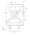
- FIG. 1 schematically illustrates a partial planar configuration of a semiconductor device (semiconductor device 1) according to an embodiment of the present disclosure.
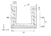
- 2A shows a cross-sectional configuration along the line AA ′ in FIG. 1
- FIG. 2B shows a cross-sectional configuration along the line BB ′ in FIG.
- the semiconductor device 1 is applied to, for example, a WCSP (wafer level package 10 in FIG. 6 described later).
- the semiconductor device 1 has a semiconductor substrate 11 provided with an alignment groove C1 and a discharge groove C2.
- the semiconductor device 1 has, for example, an insulating film 13 and a plating film 14 in this order on the semiconductor substrate 11 (FIGS. 2A and 2B).
- the semiconductor substrate 11 includes, for example, a semiconductor layer 110A and a wiring layer 110B, and has a stacked structure thereof.
- the semiconductor layer 110A is, for example, a silicon (Si) layer.
- An alignment groove C1 and a discharge groove C2 are provided in the semiconductor layer 110A.
- the wiring layer 110 ⁇ / b> B has a conductive film 12.
- the conductive film 12 is made of a metal such as copper (Cu) or aluminum (Al).
- the alignment groove C1 and the discharge groove C2 reach the conductive film 12, and the conductive film 12 forms the bottom surfaces of the alignment groove C1 and the discharge groove C2.
- the alignment groove C1 is a specific example of the first groove of the present technology
- the discharge groove C2 is a specific example of the second groove of the present technology.
- the semiconductor substrate 11 is provided with, for example, a plurality of alignment grooves C1.
- the alignment groove C1 is a mark used for alignment (positioning) when forming the plating film 14, for example.
- the upper part of the alignment groove C1 is closed by, for example, the plating film 14.
- the plurality of alignment grooves C1 are arranged side by side in one direction (X direction in FIG. 1) at a predetermined interval. Specifically, three alignment grooves C1 are arranged side by side in a region between a position P1 and a position P2 that are separated in the X direction. These three alignment grooves C1 extend in the same direction (the Y direction and the first direction in FIG. 1).
- Each alignment groove C1 has, for example, a width W1 (the size in the X direction in FIG. 1, the first width).
- the width W1 of the alignment groove C1 is, for example, several ⁇ m to several tens of ⁇ m.
- the widths W1 of the plurality of alignment grooves C1 may be different from each other.
- the lengths of the plurality of alignment grooves C1 are, for example, substantially the same, and the positions at both ends (positions in the Y direction in FIG. 1) of the plurality of alignment grooves C1 are aligned with each other. Yes.
- a discharge groove C2 connected to the ends of the plurality of alignment grooves C1 is provided, and the discharge groove C2 communicates with the alignment groove C1.
- the plating solution the plating solution 142 in FIG. 5 described later
- the upper part of the discharge groove C2 is open.
- the discharge groove C2 is connected to both ends of the alignment groove C1, for example.
- two discharge grooves C2 are provided for the three alignment grooves C1.
- One end of each of the three alignment grooves C1 is connected to one discharge groove C2, and the other end of each of the three alignment grooves C1 is connected to another discharge groove C2.
- the two discharge grooves C2 have a width W2 (the size in the Y direction in FIG. 1, the second width) that is different from the width W1 of the alignment groove C1, and a direction intersecting the extending direction of the alignment groove C1 (FIG. 1).
- the extending direction of the alignment groove C1 and the extending direction of the discharge groove C2 are orthogonal to each other.
- the widths W2 of the two discharge grooves C2 may be different from each other.
- the length L2 (the size in the X direction in FIG. 1) of the two discharge grooves C2 is, for example, substantially the same, and the positions of both ends (positions in the X direction in FIG. 1) of the two discharge grooves C2 are aligned with each other. ing.
- the discharge groove C2 is widened by a distance LD from each of the position P1 and the position P2 where the alignment groove C1 is provided.
- This distance LD preferably satisfies the following formula (1).
- t1 is the thickness of the insulating film 13 near the side wall SW2 of the discharge groove C2
- t2 is the thickness of the plating film 14 near the side wall SW2 of the discharge groove C2.
- the thicknesses t1 and t2 are maximum values considering film formation variations.
- the unit of thickness t1, t2 and width W1 is, for example, ⁇ m.
- the introduction portion from the alignment groove C1 disposed at the positions P1 and P2 (the portion connected to the alignment groove C1 in the discharge groove C2) of the discharge groove C2 is It is possible to prevent the insulating film 13 and the plating film 14 from being blocked.
- the width W2 of the discharge groove C2 is larger than the width W1 of the alignment groove C1, and preferably satisfies the following formula (2). W2> 2 ⁇ t1 + 2 ⁇ t2 (2)
- the length L2 of the discharge groove C2 preferably satisfies the distance LD from each of the positions P1 and P2 and also satisfies the following formula (3). L2> 2 ⁇ t1 + 2 ⁇ t2 (3)
- the discharge groove C2 can be prevented from being blocked by the insulating film 13 and the plating film 14, respectively.
- FIG. 3 shows another example of the configuration of the alignment groove C1 and the discharge groove C2.
- the number of alignment grooves C1 may be four or more, two, or one. It is sufficient that the discharge groove C2 is provided at least at one end of the alignment groove C1.
- one discharge groove C2 may be connected to one end of the alignment groove C1, and the other end of the alignment groove C1 may be closed.
- the semiconductor device 1 may have the alignment groove C1 and the discharge groove C2 shown in FIGS.
- the alignment groove C1 shown in FIG. 1 may be used for search alignment, and the alignment groove C1 shown in FIG. 3 may be used for fine alignment.
- the insulating film 13 is provided on one surface of the semiconductor substrate 11, more specifically, on the semiconductor layer 110A, and covers the sidewall SW1 of the alignment groove C1 and the sidewall SW2 of the discharge groove C2.
- the insulating film 13 is not provided on the bottom surfaces of the alignment groove C1 and the discharge groove C2.
- the insulating film 13 is made of, for example, silicon oxide (SiO), silicon oxynitride (SiON), silicon nitride (SiN), or the like.
- the plating film 14 is provided on the insulating film 13. In other words, the plating film 14 is provided on one surface of the semiconductor substrate 11 with the insulating film 13 therebetween.
- the plating film 14 covers the sidewall SW1 of the alignment groove C1 and the sidewall SW2 of the discharge groove C2 with the insulating film 13 therebetween.
- the plating film 14 is also provided on the bottom surfaces of the alignment groove C1 and the discharge groove C2, and is formed on the conductive film 12.
- the plating film 14 is formed using a plating method such as an electroplating method.
- the plating film 14 is made of, for example, copper (Cu), aluminum (Al), tungsten (W), titanium (Ti), gold (Au), nickel (Ni), silver (Ag), molybdenum (Mo), or tungsten titanium alloy. It is made of a metal material such as (TiW).
- the plating film 14 closes the upper part of at least one alignment groove C1.
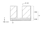
- Such a semiconductor device 1 is manufactured, for example, as follows (FIGS. 4A to 4C).
- the semiconductor substrate 11 including the semiconductor layer 110A and the wiring layer 110B is prepared.
- an alignment groove C1 and a discharge groove C2 reaching the conductive film 12 are formed in the semiconductor layer 110A of the semiconductor substrate 11 by using a photolithography method and a dry etching method.
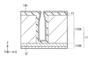
- the insulating film 13 made of, for example, silicon oxynitride (SiON) is formed over the entire surface of the semiconductor layer 110A in which the alignment groove C1 and the discharge groove C2 are formed by a CVD (Chemical Vapor Deposition: A film is formed using a chemical vapor deposition method. As a result, the insulating film 13 is formed on the side wall SW1 of the alignment groove C1 and the side wall SW2 of the discharge groove C2. The insulating film 13 formed on the bottom surfaces of the alignment groove C1 and the discharge groove C2 may be selectively removed.
- CVD Chemical Vapor Deposition: A film is formed using a chemical vapor deposition method.
- the seed layer 141 is formed over the entire surface of the semiconductor layer 110A by using, for example, a sputtering method.
- the seed layer 141 is for forming the plating film 14 and is made of, for example, copper (Cu).
- the seed layer 141 is patterned using, for example, a photolithography method and an etching method.
- the alignment groove C1 is used to align the photoresist film.
- the semiconductor substrate 11 on which the seed layer 141 is formed is immersed in a plating solution (plating solution 142 in FIG.
- the plating film 14 closes the alignment groove C1 having a small width W1.
- the opening portion of the discharge groove C2 having a sufficient width W2 and length L2 is maintained.
- the semiconductor substrate 11 is provided with the discharge groove C2 communicated with the alignment groove C1, even if the alignment groove C1 is closed during the manufacturing process, the alignment groove The substance in C1 moves to the discharge groove C2. Thereby, it is possible to suppress the occurrence of defects due to the substance being confined in the alignment groove C1.
- this operation and effect will be described.
- FIG. 5 shows a schematic cross-sectional configuration of a part of a semiconductor device (semiconductor device 100) according to a comparative example.
- this semiconductor device 100 only the alignment groove C ⁇ b> 1 is provided in the semiconductor substrate 11.
- the semiconductor substrate 11 of the semiconductor device 100 is not provided with a discharge groove (for example, the discharge groove C2 in FIG. 1).
- the alignment groove C1 may be blocked by the plating film 14 with the plating solution 142 flowing into the alignment groove C1. That is, the plating solution 142 may be trapped in the alignment groove C1.
- the plating solution 142 in the alignment groove C1 expands during heat treatment during the manufacturing process.
- the expanded plating solution 142 applies a local pressure to the semiconductor substrate 11 in the vicinity of the alignment groove C1 to generate a crack (crack 100C) or the like.
- the crack 100C is likely to occur near the interface between the semiconductor layer 110A and the wiring layer 110B.
- the alignment groove C1 Before the semiconductor substrate 11 is immersed in the plating solution 142, the alignment groove C1 may be blocked by, for example, the insulating film 13 or the like. In this case, air is trapped in the alignment groove C1. The air trapped in the alignment groove C ⁇ b> 1 may cause a malfunction in the semiconductor device 100.
- a method of sufficiently increasing the width W1 of the alignment groove C1 can be considered.
- the opening of the alignment groove C1 is maintained when the insulating film 13 and the plating film 14 are formed.
- the width W1 of the alignment groove C1 is increased, the alignment process is affected and, for example, the plating film 14 or the like may not be aligned with sufficient accuracy.
- the semiconductor substrate 11 is provided with the discharge groove C2 communicating with the alignment groove C1, even if the alignment groove C1 is blocked by the plating film 14 or the like, the alignment groove The plating solution (plating solution 142 in FIG. 5) or air in C1 moves to the discharge groove C2. Therefore, even if the semiconductor substrate 11 is subjected to heat treatment, the pressure is released through the discharge groove C2. Therefore, the occurrence of cracks (crack 100C in FIG. 5) and the like in the semiconductor substrate 11 can be suppressed.
- the semiconductor substrate 11 is provided with the discharge groove C2 communicated with the alignment groove C1, a substance (plating solution or air) is provided in the alignment groove C1. Etc.) can be prevented from occurring. Therefore, it is possible to suppress the occurrence of defects due to the alignment groove C1.
- the semiconductor device 1 of the present embodiment is applied to, for example, a WCSP (wafer level package 10 in FIG. 6 described later).
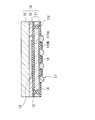
- FIG. 6 shows a schematic cross-sectional configuration of a wafer level package 10 to which the semiconductor device 1 is applied.
- the wafer level package 10 is a WCSP (wafer level chip size package) in which, for example, a light receiving element 19 (functional element) is sealed between a semiconductor substrate 11 and a glass substrate 16 (sealing substrate).
- the semiconductor substrate 11 and the glass substrate 16 are bonded to each other at the peripheral portion via the adhesive layer 15, and a region surrounded by the semiconductor substrate 11, the glass substrate 16, and the adhesive layer 15 hermetically seals the light receiving element 19. It is a cavity to stop.
- the wafer level package 10 is used in an optical apparatus such as an image sensor device.
- the semiconductor substrate 11 side of the wafer level package 10 is mounted on a printed board such as a mother board, and the glass substrate 16 side of the wafer level package 10 is bonded to, for example, a lens unit.
- the wiring layer 110B of the semiconductor substrate 11 is disposed on the glass substrate 16 side, and the semiconductor layer 110A of the semiconductor substrate 11 faces the glass substrate 16 with the wiring layer 110B in between. That is, the alignment groove C1 and the discharge groove C2 (FIGS. 2A and 2B) are provided on the surface of the semiconductor substrate 11 opposite to the surface facing the glass substrate 16.
- the light receiving element 19 is provided in contact with the wiring layer 110B, for example.
- the conductive film 12 of the wiring layer 110 ⁇ / b> B is disposed, for example, on the peripheral edge of the semiconductor substrate 11 (portion facing the adhesive layer 15).
- the conductive film 12 is connected to the light receiving element 19 and its peripheral circuit by wiring (not shown).
- the conductive film 12 functions as, for example, an external connection pad for inputting an electrical signal to the light receiving element 19 and its peripheral circuit or for taking out an electrical signal output from the electrical signal.
- the light receiving element 19 is a solid-state image sensor such as a CCD (Charge-Coupled Device) or a CMOS (Complementary Metal-Oxide-Semiconductor), for example, and a light filter (not shown) is provided on the light receiving surface.
- a CCD Charge-Coupled Device
- CMOS Complementary Metal-Oxide-Semiconductor
- a light filter (not shown) is provided on the light receiving surface.
- exposure and light reception signal are read out in accordance with an electric signal input through the conductive film 12, and the read light reception signal is output to the outside through the conductive film 12.
- a solder ball 17 and a sealing resin layer 18 are disposed on the semiconductor layer 110A together with the plating film 14.
- the plating film 14 is provided in a selective region on the semiconductor layer 110 ⁇ / b> A, and solder balls 17 are connected to the plating film 14.
- the sealing resin layer 18 has an opening that covers the plating film 14 and exposes the plating film 14. Solder balls 17 are provided in the openings of the sealing resin layer 18.
- a through via 11V is provided at a position corresponding to the conductive film 12 of the wiring layer 110B.
- the through via 11V penetrates from the front surface to the back surface of the semiconductor layer 110A, whereby a part of the conductive film 12 is exposed.
- a plated film 14 is formed inside the through via 11V so as to cover the exposed surface of the conductive film 12, and extends from the inside of the through via 11V to the formation region of the solder ball 17 on the semiconductor layer 110A. It is set (drawn). Note that the insulating film 13 and the seed layer 141 (FIG. 4C) are formed between the semiconductor layer 110A and the plating film.
- the through via 11V has, for example, a circular planar shape with a diameter of about 60 ⁇ m.
- the alignment groove C1 and the discharge groove C2 are formed in the same process as the through via 11V.
- the solder ball 17 functions as an external connection terminal for mounting on a printed board, and is made of, for example, lead-free high melting point solder such as Sn—Ag—Cu.
- the plurality of solder balls 17 are regularly arranged at a predetermined pitch on the semiconductor layer 110A.
- the arrangement of the solder balls 17 is appropriately set according to the position of the bonding pad on the printed circuit board (not shown) side to be mounted. Thereby, the arrangement of the conductive film 12 is converted into the arrangement of the solder balls 17 and can be directly mounted on a printed board such as a mother board.
- the solder balls 17 are not formed near the center of the semiconductor substrate 11, but of course, the solder balls 17 may be arranged near the center or in the peripheral region. May be provided.
- the solder ball 17 is electrically connected to the conductive film 12 through the plating film 14.
- the plating film 14 provided in the through via 11V is for electrically connecting the solder ball 17 and the conductive film 12, and functions as a rewiring.
- the sealing resin layer 18 is for protecting the plating film 14 and has an opening corresponding to the solder ball 17.
- the sealing resin layer 18 is made of, for example, an epoxy resin, a polyimide resin, a silicon resin, an acrylic resin, or the like.
- the conductive film 12 of the wiring layer 110B and the solder ball 17 on the semiconductor layer 110A are electrically connected through the through via 11V and the plating film 14.
- the external connection terminals are drawn from one surface (surface on the wiring layer 110B side) of the semiconductor substrate 11 to the other surface (semiconductor layer 110A) (the external connection terminals are converted from the conductive film 12 to the solder balls 17).
- the semiconductor substrate 11 of the wafer level package 10 has the discharge groove C2 communicated with the alignment groove C1, the occurrence of defects due to the alignment groove C1 can be suppressed. Therefore, the yield of the wafer level package 10 can be improved.
- the film may be formed using a method other than the plating method.
- the method other than the plating method include a CVD method, a physical vapor deposition (PVD) method, an atomic layer deposition (ALD) method, a sputtering method, and the like.
- the alignment groove C1 is used for alignment of the plating film 14 has been described.
- the alignment groove C1 may be used for alignment of other films.
- the alignment groove C1 is closed by the plating film 14.
- the alignment groove C1 may be closed by another film such as the insulating film 13, or the like. The opening may be maintained.
- the alignment groove C1 and the discharge groove C2 have been described as examples.
- the alignment groove C1 and the discharge groove C2 have a groove shape as long as the effect of the present disclosure can be exhibited. You don't have to.
- the case where the light receiving element 19 is used as the functional element has been described.
- a functional element other than the light receiving element may be used.
- MEMS Micro Electro Mechanical System
- MEMS Micro Electro Mechanical System
- the present disclosure may be configured as follows. (1) A semiconductor substrate; A first groove provided in the semiconductor substrate and having a first width W1 and extending in a first direction; A second groove provided in the semiconductor substrate in communication with the first groove and having a second width W2 different from the first width and extending in a second direction intersecting the first direction; Prepared, One of the first groove and the second groove is used for alignment. Semiconductor device. (2) The semiconductor device according to (1), wherein the second width W2 is larger than the first width W1. (3) The first groove is used for the alignment; The semiconductor device according to (1) or (2), wherein the second groove is used for discharging the material that has flowed into the first groove.
- the second groove is provided with a distance LD widened from each of the first position and the second position,
- the distance LD satisfies the following formula (1):
- the semiconductor device according to (6) or (7), wherein the second width W2 of the second groove satisfies the following formula (2). W2> 2 ⁇ t1 + 2 ⁇ t2 (2)
Landscapes
- Internal Circuitry In Semiconductor Integrated Circuit Devices (AREA)
- Electrodes Of Semiconductors (AREA)
- Solid State Image Pick-Up Elements (AREA)
Abstract
半導体基板と、前記半導体基板に設けられ、第1の幅W1を有して第1方向に延在する第1溝と、前記第1溝に連通して前記半導体基板に設けられ、前記第1の幅と異なる第2の幅W2を有して前記第1方向に交差する第2方向に延在する第2溝とを備え、前記第1溝および前記第2溝のいずれか一方がアライメントに用いられる半導体装置。
Description
本開示は、半導体基板を有する半導体装置に関する。
近年、WCSP(Wafer level Chip Size Package)等の半導体装置の開発が進められている。WCSPは、例えば、半導体基板と封止基板との間に、受光素子等の機能素子を有している(例えば、特許文献1参照)。
半導体基板の一方の面には、例えば、貫通電極、再配線層および半田ボール等が設けられている。各部材を半導体基板上に形成する工程では、例えば、半導体基板にアライメント溝を形成して、位置の調整が行われる。
このようなアライメント溝が設けられた半導体装置では、アライメント溝に起因した不具合の発生を抑えることが望まれている。
したがって、アライメント溝に起因した不具合の発生を抑えることが可能な半導体装置を提供することが望ましい。
本開示の一実施の形態に係る半導体装置は、半導体基板と、半導体基板に設けられ、第1の幅W1を有して第1方向に延在する第1溝と、第1溝に連通して半導体基板に設けられ、第1の幅と異なる第2の幅W2を有して第1方向に交差する第2方向に延在する第2溝とを備え、第1溝および第2溝のいずれか一方がアライメントに用いられるものである。
本開示の一実施の形態に係る半導体装置では、第1溝に連通された第2溝が設けられているので、仮に、製造過程で、アライメント溝(第1溝または第2溝)が塞がれても、アライメント溝中の物質は、もう一方の溝に移動する。
本開示の一実施の形態に係る半導体装置によれば、第1溝に連通された第2溝を設けるようにしたので、例えば、アライメント溝中に物質が閉じ込められることに起因した不具合の発生を抑えることができる。よって、アライメント溝に起因した不具合の発生を抑えることが可能となる。
尚、上記内容は本開示の一例である。本開示の効果は、上述したものに限らず、他の異なる効果であってもよいし、更に他の効果を含んでいてもよい。
以下、本開示における実施形態について、図面を参照して詳細に説明する。なお、説明する順序は、下記の通りである。
1.実施の形態(アライメント溝および排出溝を有する半導体装置)
2.適用例(WCSPの例)
1.実施の形態(アライメント溝および排出溝を有する半導体装置)
2.適用例(WCSPの例)
<実施の形態>
図1は、本開示の一実施の形態に係る半導体装置(半導体装置1)の一部の平面構成を模式的に表したものである。図2Aは、図1のA-A’線に沿った断面構成、図2Bは、図1のB-B’線に沿った断面構成を表している。この半導体装置1は、例えば、WCSP(後述の図6のウェハレベルパッケージ10)などに適用される。半導体装置1は、アライメント溝C1および排出溝C2が設けられた半導体基板11を有している。半導体装置1は、この半導体基板11上に、例えば、絶縁膜13およびメッキ膜14をこの順に有している(図2A,図2B)。
図1は、本開示の一実施の形態に係る半導体装置(半導体装置1)の一部の平面構成を模式的に表したものである。図2Aは、図1のA-A’線に沿った断面構成、図2Bは、図1のB-B’線に沿った断面構成を表している。この半導体装置1は、例えば、WCSP(後述の図6のウェハレベルパッケージ10)などに適用される。半導体装置1は、アライメント溝C1および排出溝C2が設けられた半導体基板11を有している。半導体装置1は、この半導体基板11上に、例えば、絶縁膜13およびメッキ膜14をこの順に有している(図2A,図2B)。
半導体基板11は、例えば、半導体層110Aおよび配線層110Bを含み、これらの積層構造を有している。半導体層110Aは、例えば、シリコン(Si)層である。この半導体層110Aに、アライメント溝C1および排出溝C2が設けられている。配線層110Bは、導電膜12を有している。導電膜12は、例えば銅(Cu)またはアルミニウム(Al)等の金属により構成されている。アライメント溝C1および排出溝C2は、導電膜12に達しており、導電膜12によりアライメント溝C1および排出溝C2の底面が構成されている。なお、アライメント溝C1が本技術の第1溝の一具体例であり、排出溝C2が本技術の第2溝の一具体例である。
半導体基板11には、例えば複数のアライメント溝C1が設けられている。アライメント溝C1は、例えば、メッキ膜14を形成する際のアライメント(位置決め)に用いられる目印である。このアライメント溝C1の上部は、例えば、メッキ膜14により塞がれている。複数のアライメント溝C1は、互いに所定の間隔で一方向(図1のX方向)に並んで配置されている。具体的には、X方向に離間する位置P1から位置P2までの間の領域に3つのアライメント溝C1が、並んで配置されている。これら3つのアライメント溝C1は、同一の方向(図1のY方向,第1方向)に延在している。各々のアライメント溝C1は、例えば幅W1(図1のX方向の大きさ,第1の幅)を有している。アライメント溝C1の幅W1は、例えば数μm~数十μmである。複数のアライメント溝C1の幅W1が、互いに異なっていてもよい。複数のアライメント溝C1の長さ(図1のY方向の大きさ)は、例えば、略同じであり、複数のアライメント溝C1の両端の位置(図1のY方向の位置)は、互いに揃っている。
本実施の形態では、複数のアライメント溝C1の端に接続された排出溝C2が設けられており、アライメント溝C1に排出溝C2が連通している。これにより、アライメント溝C1が、仮に、メッキ膜14等により塞がれても、アライメント溝C1中のメッキ液(後述の図5のメッキ液142)が、排出溝C2に移動する。この排出溝C2の上部は開放されている。
排出溝C2は、例えば、アライメント溝C1の両端に接続されている。具体的には、3つのアライメント溝C1に対して、2つの排出溝C2が設けられている。3つのアライメント溝C1の一方の端各々が、1つの排出溝C2に接続されており、3つのアライメント溝C1の他方の端各々が、もう1つの排出溝C2に接続されている。2つの排出溝C2は、アライメント溝C1の幅W1と異なる幅W2(図1のY方向の大きさ,第2の幅)を有し、アライメント溝C1の延在方向と交差する方向(図1のX方向,第2方向)に延在している。例えば、アライメント溝C1の延在方向と、排出溝C2の延在方向とは、直交している。2つの排出溝C2の幅W2が、互いに異なっていてもよい。2つの排出溝C2の長さL2(図1のX方向の大きさ)は、例えば、略同じであり、2つの排出溝C2の両端の位置(図1のX方向の位置)は、互いに揃っている。
排出溝C2は、アライメント溝C1が設けられた位置P1,位置P2各々から、距離LDだけ拡幅して設けられている。この距離LDは、以下の式(1)を満たすことが好ましい。
LD>t1+t2-W1/2 ・・・・・(1)
ここで、t1は、排出溝C2の側壁SW2近傍での絶縁膜13の厚みであり、t2は排出溝C2の側壁SW2近傍でのメッキ膜14の厚みである。厚みt1,t2は、成膜ばらつきを考慮した最大値である。厚みt1,t2および幅W1の単位は、例えばμmである。
LD>t1+t2-W1/2 ・・・・・(1)
ここで、t1は、排出溝C2の側壁SW2近傍での絶縁膜13の厚みであり、t2は排出溝C2の側壁SW2近傍でのメッキ膜14の厚みである。厚みt1,t2は、成膜ばらつきを考慮した最大値である。厚みt1,t2および幅W1の単位は、例えばμmである。
距離LDが式(1)を満たすことにより、排出溝C2のうち、位置P1,P2に配置されたアライメント溝C1からの導入部(排出溝C2のうち、アライメント溝C1との連結部分)が、絶縁膜13およびメッキ膜14により塞がれるのを抑えることができる。
排出溝C2の幅W2は、アライメント溝C1の幅W1よりも大きくなっており、以下の式(2)を満たすことが好ましい。
W2>2×t1+2×t2 ・・・・・(2)
W2>2×t1+2×t2 ・・・・・(2)
排出溝C2の長さL2は、上記の位置P1,P2各々からの距離LDを満たすとともに、下記の式(3)を満たすことが好ましい。
L2>2×t1+2×t2 ・・・・・(3)
L2>2×t1+2×t2 ・・・・・(3)
排出溝C2の幅W2および長さL2が各々、上記の式(2),(3)を満たすことにより、排出溝C2が、絶縁膜13およびメッキ膜14により塞がれるのを抑えることができる。
図3は、アライメント溝C1および排出溝C2の構成の他の例を表している。アライメント溝C1は、4つ以上または2つであってもよく、あるいは、1つであってもよい。少なくとも、アライメント溝C1の一方の端に排出溝C2が設けられていればよい。例えば、アライメント溝C1の一方の端に1つの排出溝C2が接続されており、アライメント溝C1の他方の端が、閉じられていてもよい。例えば、半導体装置1が、図1および図3に示したアライメント溝C1,排出溝C2を有していてもよい。図1に示したアライメント溝C1を、サーチアライメントに用い、図3に示したアライメント溝C1を、ファインアライメントに用いるようにしてもよい。
絶縁膜13は、半導体基板11の一方の面上、より具体的には、半導体層110A上に設けられ、アライメント溝C1の側壁SW1および排出溝C2の側壁SW2を覆っている。アライメント溝C1および排出溝C2の底面には、絶縁膜13が設けられていない。この絶縁膜13は、例えば、酸化シリコン(SiO),酸窒化シリコン(SiON)または窒化シリコン(SiN)等により構成されている。
メッキ膜14は、絶縁膜13上に設けられている。換言すれば、メッキ膜14は、絶縁膜13を間にして半導体基板11の一方の面上に設けられている。このメッキ膜14は、絶縁膜13を間にして、アライメント溝C1の側壁SW1および排出溝C2の側壁SW2を覆っている。メッキ膜14は、アライメント溝C1および排出溝C2の底面にも設けられ、導電膜12上に成膜されている。このメッキ膜14は、例えば電気メッキ法等のメッキ法を用いて成膜されたものである。メッキ膜14は、例えば、銅(Cu),アルミニウム(Al),タングステン(W),チタン(Ti),金(Au),ニッケル(Ni),銀(Ag),モリブデン(Mo)またはタングステンチタン合金(TiW)等の金属材料により構成されている。メッキ膜14は少なくとも1つのアライメント溝C1の上部を塞いでいる。
このような半導体装置1は、例えば、以下のようにして製造する(図4A~図4C)。
まず、半導体層110Aおよび配線層110Bを含む半導体基板11を用意する。次いで、図4Aに示したように、この半導体基板11の半導体層110Aに、フォトリソグラフイ法およびドライエッチング法を用いて、導電膜12に達するアライメント溝C1および排出溝C2を形成する。
続いて、図4Bに示したように、アライメント溝C1および排出溝C2を形成した半導体層110Aの全面にわたって、例えば、酸窒化シリコン(SiON)よりなる絶縁膜13を、CVD法(Chemical Vapor Deposition:化学気相成長法)を用いて成膜する。これにより、アライメント溝C1の側壁SW1および排出溝C2の側壁SW2に絶縁膜13が形成される。アライメント溝C1および排出溝C2の底面に成膜された絶縁膜13は、選択的に除去するようにしてもよい。
絶縁膜13を成膜した後、図4Cに示したように、半導体層110Aの全面にわたって、例えば、スパッタ法を用いてシード層141を形成する。シード層141は、メッキ膜14を形成するためのものであり、例えば銅(Cu)により構成されている。シード層141を成膜した後、例えばフォトリソグラフィ法およびエッチッグ法を用いて、シード層141のパターニングを行う。このシード層141のパターニングの際に、例えば、アライメント溝C1が用いられて、フォトレジスト膜のアライメントが行われる。この後、シード層141が形成された半導体基板11を、例えば硫酸銅(CuSO4)からなるメッキ液(後述の図5のメッキ液142)に浸けてメッキ膜14を形成する。例えば、このメッキ膜14により、小さな幅W1のアライメント溝C1は塞がれる。十分な幅W2および長さL2を有する排出溝C2の開口部分は維持される。このような工程を経て、図1等に示した半導体装置1を完成させる。
本実施の形態の半導体装置1では、半導体基板11に、アライメント溝C1に連通された排出溝C2が設けられているので、仮に、製造過程で、アライメント溝C1が塞がれても、アライメント溝C1中の物質は、排出溝C2に移動する。これにより、アライメント溝C1中に物質が閉じ込められることに起因した不具合の発生を抑えることができる。以下、この作用・効果について説明する。
図5は、比較例に係る半導体装置(半導体装置100)の一部の模式的な断面構成を表している。この半導体装置100では、半導体基板11にアライメント溝C1のみが設けられている。換言すれば、半導体装置100の半導体基板11には、排出溝(例えば図1の排出溝C2)が設けられていない。このような半導体装置100では、メッキ膜14を形成する際に、アライメント溝C1内にメッキ液142が流入した状態のまま、メッキ膜14によりアライメント溝C1が塞がれるおそれがある。即ち、アライメント溝C1中に、メッキ液142が閉じ込められるおそれがある。このアライメント溝C1中のメッキ液142は、製造工程中の熱処理の際に膨張する。膨張したメッキ液142により、アライメント溝C1近傍の半導体基板11に局所的な圧力が加えられ、クラック(クラック100C)等が発生する。クラック100Cは、例えば、半導体層110Aと配線層110Bとの界面近傍で発生しやすい。
半導体基板11をメッキ液142に浸ける前に、例えば、絶縁膜13等により、アライメント溝C1が塞がれることも考え得る。この場合には、アライメント溝C1中に空気が閉じこめられる。このアライメント溝C1中に閉じ込められた空気が、半導体装置100に不具合を生じさせるおそれがある。
また、アライメント溝C1の幅W1を十分大きくする方法も考え得る。この方法では、絶縁膜13およびメッキ膜14等を形成する際に、アライメント溝C1の開口が維持される。しかし、アライメント溝C1の幅W1を大きくすると、アライメント工程に影響が及び、例えば、十分な精度でメッキ膜14等のアライメントを行うことができないおそれがある。
これに対し、本実施の形態では、半導体基板11に、アライメント溝C1に連通した排出溝C2が設けられているので、仮に、アライメント溝C1がメッキ膜14等により塞がれても、アライメント溝C1中のメッキ液(図5のメッキ液142)または空気等は、排出溝C2に移動する。したがって、半導体基板11に熱処理が施されても、排出溝C2を介して圧力が開放される。よって、半導体基板11でのクラック(図5のクラック100C)等の発生が抑えられる。
また、アライメント溝C1の幅W1を大きくする必要がないので、アライメント工程に影響を及ぼすことなく、半導体基板11でのクラック等の発生が抑えられる。
以上説明したように、本実施の形態に係る半導体装置1では、半導体基板11に、アライメント溝C1に連通された排出溝C2を設けるようにしたので、アライメント溝C1中に物質(メッキ液または空気等)が閉じ込められることに起因した不具合の発生を抑えることができる。よって、アライメント溝C1に起因した不具合の発生を抑えることが可能となる。
<適用例>
本実施の形態の半導体装置1は例えばWCSP(後述の図6のウェハレベルパッケージ10)に適用される。
本実施の形態の半導体装置1は例えばWCSP(後述の図6のウェハレベルパッケージ10)に適用される。
図6は、半導体装置1が適用されたウェハレベルパッケージ10の模式的な断面構成を表すものである。このウェハレベルパッケージ10は、半導体基板11とガラス基板16(封止基板)との間に、例えば受光素子19(機能素子)を封止してなるWCSP(ウェハレベルチップサイズパッケージ)である。半導体基板11とガラス基板16とは、これらの周縁部において接着層15を介して貼り合わせられ、これらの半導体基板11、ガラス基板16および接着層15によって囲まれる領域が、受光素子19を気密封止するためのキャビティとなっている。このウェハレベルパッケージ10は、例えばイメージセンサ装置等の光学機器に使用される。ウェハレベルパッケージ10の半導体基板11側は、マザーボード等のプリント基板へ実装され、ウェハレベルパッケージ10のガラス基板16側は、例えば、レンズユニットに貼り合わされる。
半導体基板11の配線層110Bはガラス基板16側に配置され、半導体基板11の半導体層110Aは、配線層110Bを間にしてガラス基板16に対向している。即ち、アライメント溝C1および排出溝C2(図2A,図2B)は、半導体基板11の、ガラス基板16との対向面と反対の面に設けられている。受光素子19は、例えば、配線層110Bに接して設けられている。
配線層110Bの導電膜12は、例えば、半導体基板11の周縁部(接着層15に対向する部分)に配置されている。この導電膜12は、例えば、受光素子19やその周辺回路へ配線(図示せず)によって接続されている。導電膜12は、例えば、受光素子19やその周辺回路に電気信号を入力したり、あるいはそれらから出力された電気信号を取り出すための外部接続用のパッドとして機能する。
受光素子19は、例えばCCD(Charge Coupled Device)やCMOS(Complementary Metal Oxide Semiconductor)等の固体撮像素子であり、受光面には、図示しないカラーフィルタが設けられている。この受光素子19では、導電膜12を通じて入力された電気信号に応じて、露光および受光信号の読み出しが行われ、読み出された受光信号が導電膜12を通じて外部へ出力されるようになっている。
半導体層110A上には、メッキ膜14とともに、半田ボール17および封止樹脂層18が配設されている。メッキ膜14は、半導体層110A上の選択的な領域に設けられており、このメッキ膜14に半田ボール17が接続されている。封止樹脂層18は、メッキ膜14を覆うとともに、メッキ膜14を露出させる開口を有している。この封止樹脂層18の開口に半田ボール17が設けられている。
半導体層110Aには、配線層110Bの導電膜12に対応する位置に貫通ビア11Vが設けられている。貫通ビア11Vは、半導体層110Aの表面から裏面までを貫通しており、これによって導電膜12の一部が露出している。この貫通ビア11Vの内部には、メッキ膜14が、露出された導電膜12の表面を覆って形成されており、かつ貫通ビア11Vの内部から半導体層110A上の半田ボール17の形成領域まで延設されている(引き出されている)。尚、半導体層110Aとメッキ膜14との間には、上述の絶縁膜13およびシード層141(図4C)が形成されている。貫通ビア11Vは、例えば、直径60μm程度の円状の平面形状を有している。例えば、この貫通ビア11Vの形成工程と、同一工程で、アライメント溝C1および排出溝C2が形成される。
半田ボール17は、プリント基板へ実装するための外部接続端子として機能するものであり、例えばSn-Ag-Cu等の無鉛高融点はんだ等よりなる。例えば、複数の半田ボール17が、半導体層110A上に、所定のピッチで規則的に配列して設けられている。この半田ボール17の配列は、実装されるプリント基板(図示せず)側の接合パッドの位置に応じて適宜設定されている。これにより、導電膜12の配列が半田ボール17の配列に変換され、マザーボード等のプリント基板へ直接実装することが可能となる。尚、図6では、半田ボール17が半導体基板11の中央付近には形成されていない配列となっているが、勿論中央付近にも半田ボール17が配設されていてもよいし、周縁領域にのみ配設されていてもよい。この半田ボール17は、メッキ膜14を介して導電膜12と電気的に接続されている。
貫通ビア11Vに設けられたメッキ膜14は、半田ボール17と導電膜12とを電気的に接続するためのものであり、再配線として機能する。
封止樹脂層18は、メッキ膜14を保護するためのものであり、半田ボール17に対応して開口を有している。この封止樹脂層18は、例えばエポキシ系、ポリイミド系、シリコン系、アクリル系の樹脂等により構成されている。
このウェハレベルパッケージ10では、配線層110Bの導電膜12と半導体層110A上の半田ボール17とが、貫通ビア11Vおよびメッキ膜14を介して電気的に接続されている。これにより、半導体基板11の一方の面(配線層110B側の面)から他方の面(半導体層110A)側へ外部接続端子が引き出される(外部接続端子が導電膜12から半田ボール17へ変換される)。
ウェハレベルパッケージ10の半導体基板11が、アライメント溝C1に連通した排出溝C2を有することにより、アライメント溝C1に起因した不具合の発生が抑えられる。よって、ウェハレベルパッケージ10の歩留まりを向上させることが可能となる。
以上、実施の形態および適用例を挙げて説明したが、本開示内容は上記実施の形態等に限定されるものではなく、種々変形が可能である。例えば、上記実施の形態において説明した半導体装置の構成は一例であり、更に他の層を備えていてもよい。また、各層の材料や厚みも一例であって、上述のものに限定されるものではない。
例えば、上記実施の形態では、半導体基板11上にメッキ膜14を成膜する場合について説明したが、メッキ法以外の方法を用いて膜を形成するようにしてもよい。メッキ法以外の方法とは、例えば、CVD法,物理気相成長(PVD:Physical Vapor Deposition)法,原子層堆積(ALD:Atomic Layer Deposition)法またはスパッタ法等である。
また、上記実施の形態では、アライメント溝C1を、メッキ膜14のアライメントに用いる場合について説明したが、アライメント溝C1は、他の膜のアライメントに用いるようにしてもよい。
また、図2Aには、アライメント溝C1がメッキ膜14により塞がれている例を示したが、アライメント溝C1は、例えば絶縁膜13など、他の膜によって塞がれていてもよく、あるいは、開口が維持されていてもよい。
また、図1および図3では、複数のアライメント溝C1が同一方向に並んで配置されている例を示したが、複数のアライメント溝C1が互いに交差する方向に配置されていてもよい。更に、上記実施の形態では、アライメント溝C1および排出溝C2を例に挙げて説明したが、本開示の効果を発揮し得る態様であれば、アライメント溝C1および排出溝C2は、溝形状を有していなくてもよい。
また、上記適用例では、機能素子として、受光素子19を用いる場合について説明したが、受光素子以外の機能素子を用いるようにしてもよい。例えば、MEMS(Micro Electro Mechanical System)を用いるようにしてもよい。
上記実施の形態等において説明した効果は一例であり、他の効果であってもよいし、更に他の効果を含んでいてもよい。
尚、本開示は、以下のような構成であってもよい。
(1)
半導体基板と、
前記半導体基板に設けられ、第1の幅W1を有して第1方向に延在する第1溝と、
前記第1溝に連通して前記半導体基板に設けられ、前記第1の幅と異なる第2の幅W2を有して前記第1方向に交差する第2方向に延在する第2溝と
を備え、
前記第1溝および前記第2溝のいずれか一方がアライメントに用いられる
半導体装置。
(2)
前記第2の幅W2は、前記第1の幅W1よりも大きい
前記(1)に記載の半導体装置。
(3)
前記第1溝が前記アライメントに用いられ、
前記第2溝が前記第1溝に流入した物質の排出に用いられる
前記(1)または(2)に記載の半導体装置。
(4)
前記第2方向に離間する第1の位置から第2の位置までの領域に、所定の間隔で配置された複数の前記第1溝を有し、
前記複数の前記第1溝の少なくとも一方の端に前記第2溝が設けられている
前記(3)に記載の半導体装置。
(5)
前記複数の前記第1溝の両端に前記第2溝が設けられている
前記(4)に記載の半導体装置。
(6)
更に、前記第1溝の側壁および前記第2溝の側壁に設けられ、厚みt1を有する絶縁膜と、
前記絶縁膜に積層された、厚みt2を有するメッキ膜とを有する
前記(4)または(5)に記載の半導体装置。
(7)
前記第2溝は、前記第1の位置および前記第2の位置各々から、距離LD拡幅して設けられ、
距離LDは、以下の式(1)を満たす
前記(6)に記載の半導体装置。
LD>t1+t2-W1/2 ・・・・・(1)
(8)
前記第2溝の前記第2の幅W2は、以下の式(2)を満たす
前記(6)または(7)に記載の半導体装置。
W2>2×t1+2×t2 ・・・・・(2)
(9)
前記第2溝は開放されている
前記(6)ないし(8)のうちいずれか1つに記載の半導体装置。
(10)
前記第1溝は、前記絶縁膜または前記メッキ膜により塞がれている
前記(6)ないし(9)のうちいずれか1つに記載の半導体装置。
(11)
更に、前記第1溝および前記第2溝の底に設けられた導電膜を含む
前記(1)ないし(10)のうちいずれか1つに記載の半導体装置。
(12)
前記半導体基板はシリコン層を含む
前記(1)ないし(11)のうちいずれか1つに記載の半導体装置。
(13)
更に、前記半導体基板に対向する封止基板と、
前記封止基板と前記半導体基板との間に設けられた機能素子とを含み、
前記第1溝および前記第2溝は、前記半導体基板の前記封止基板との対向面と反対の面に設けられている
前記(1)ないし(12)のうちいずれか1つに記載の半導体装置。
(14)
前記第1方向および前記第2方向は、直交している
前記(1)ないし(13)のうちいずれか1つに記載の半導体装置。
(1)
半導体基板と、
前記半導体基板に設けられ、第1の幅W1を有して第1方向に延在する第1溝と、
前記第1溝に連通して前記半導体基板に設けられ、前記第1の幅と異なる第2の幅W2を有して前記第1方向に交差する第2方向に延在する第2溝と
を備え、
前記第1溝および前記第2溝のいずれか一方がアライメントに用いられる
半導体装置。
(2)
前記第2の幅W2は、前記第1の幅W1よりも大きい
前記(1)に記載の半導体装置。
(3)
前記第1溝が前記アライメントに用いられ、
前記第2溝が前記第1溝に流入した物質の排出に用いられる
前記(1)または(2)に記載の半導体装置。
(4)
前記第2方向に離間する第1の位置から第2の位置までの領域に、所定の間隔で配置された複数の前記第1溝を有し、
前記複数の前記第1溝の少なくとも一方の端に前記第2溝が設けられている
前記(3)に記載の半導体装置。
(5)
前記複数の前記第1溝の両端に前記第2溝が設けられている
前記(4)に記載の半導体装置。
(6)
更に、前記第1溝の側壁および前記第2溝の側壁に設けられ、厚みt1を有する絶縁膜と、
前記絶縁膜に積層された、厚みt2を有するメッキ膜とを有する
前記(4)または(5)に記載の半導体装置。
(7)
前記第2溝は、前記第1の位置および前記第2の位置各々から、距離LD拡幅して設けられ、
距離LDは、以下の式(1)を満たす
前記(6)に記載の半導体装置。
LD>t1+t2-W1/2 ・・・・・(1)
(8)
前記第2溝の前記第2の幅W2は、以下の式(2)を満たす
前記(6)または(7)に記載の半導体装置。
W2>2×t1+2×t2 ・・・・・(2)
(9)
前記第2溝は開放されている
前記(6)ないし(8)のうちいずれか1つに記載の半導体装置。
(10)
前記第1溝は、前記絶縁膜または前記メッキ膜により塞がれている
前記(6)ないし(9)のうちいずれか1つに記載の半導体装置。
(11)
更に、前記第1溝および前記第2溝の底に設けられた導電膜を含む
前記(1)ないし(10)のうちいずれか1つに記載の半導体装置。
(12)
前記半導体基板はシリコン層を含む
前記(1)ないし(11)のうちいずれか1つに記載の半導体装置。
(13)
更に、前記半導体基板に対向する封止基板と、
前記封止基板と前記半導体基板との間に設けられた機能素子とを含み、
前記第1溝および前記第2溝は、前記半導体基板の前記封止基板との対向面と反対の面に設けられている
前記(1)ないし(12)のうちいずれか1つに記載の半導体装置。
(14)
前記第1方向および前記第2方向は、直交している
前記(1)ないし(13)のうちいずれか1つに記載の半導体装置。
本出願は、日本国特許庁において2018年2月1日に出願された日本特許出願番号第2018-16513号を基礎として優先権を主張するものであり、この出願の全ての内容を参照によって本出願に援用する。
当業者であれば、設計上の要件や他の要因に応じて、種々の修正、コンビネーション、サブコンビネーション、および変更を想到し得るが、それらは添付の請求の範囲やその均等物の範囲に含まれるものであることが理解される。
Claims (14)
- 半導体基板と、
前記半導体基板に設けられ、第1の幅W1を有して第1方向に延在する第1溝と、
前記第1溝に連通して前記半導体基板に設けられ、前記第1の幅と異なる第2の幅W2を有して前記第1方向に交差する第2方向に延在する第2溝と
を備え、
前記第1溝および前記第2溝のいずれか一方がアライメントに用いられる
半導体装置。 - 前記第2の幅W2は、前記第1の幅W1よりも大きい
請求項1に記載の半導体装置。 - 前記第1溝が前記アライメントに用いられ、
前記第2溝が前記第1溝に流入した物質の排出に用いられる
請求項2に記載の半導体装置。 - 前記第2方向に離間する第1の位置から第2の位置までの領域に、所定の間隔で配置された複数の前記第1溝を有し、
前記複数の前記第1溝の少なくとも一方の端に前記第2溝が設けられている
請求項3に記載の半導体装置。 - 前記複数の前記第1溝の両端に前記第2溝が設けられている
請求項4に記載の半導体装置。 - 更に、前記第1溝の側壁および前記第2溝の側壁に設けられ、厚みt1を有する絶縁膜と、
前記絶縁膜に積層された、厚みt2を有するメッキ膜とを有する
請求項4に記載の半導体装置。 - 前記第2溝は、前記第1の位置および前記第2の位置各々から、距離LD拡幅して設けられ、
距離LDは、以下の式(1)を満たす
請求項6に記載の半導体装置。
LD>t1+t2-W1/2 ・・・・・(1)
- 前記第2溝の前記第2の幅W2は、以下の式(2)を満たす
請求項6に記載の半導体装置。
W2>2×t1+2×t2 ・・・・・(2)
- 前記第2溝は開放されている
請求項6に記載の半導体装置。 - 前記第1溝は、前記絶縁膜または前記メッキ膜により塞がれている
請求項6に記載の半導体装置。 - 更に、前記第1溝および前記第2溝の底に設けられた導電膜を含む
請求項1に記載の半導体装置。 - 前記半導体基板はシリコン層を含む
請求項1に記載の半導体装置。 - 更に、前記半導体基板に対向する封止基板と、
前記封止基板と前記半導体基板との間に設けられた機能素子とを含み、
前記第1溝および前記第2溝は、前記半導体基板の前記封止基板との対向面と反対の面に設けられている
請求項1に記載の半導体装置。 - 前記第1方向および前記第2方向は、直交している
請求項1に記載の半導体装置。
Priority Applications (3)
| Application Number | Priority Date | Filing Date | Title |
|---|---|---|---|
| DE112019000652.5T DE112019000652T5 (de) | 2018-02-01 | 2019-01-08 | Halbleitervorrichtung |
| US16/964,654 US11515349B2 (en) | 2018-02-01 | 2019-01-08 | Semiconductor unit |
| CN201980009898.XA CN111656496B (zh) | 2018-02-01 | 2019-01-08 | 半导体装置 |
Applications Claiming Priority (2)
| Application Number | Priority Date | Filing Date | Title |
|---|---|---|---|
| JP2018016513A JP2019134111A (ja) | 2018-02-01 | 2018-02-01 | 半導体装置 |
| JP2018-016513 | 2018-02-01 |
Publications (1)
| Publication Number | Publication Date |
|---|---|
| WO2019150888A1 true WO2019150888A1 (ja) | 2019-08-08 |
Family
ID=67478742
Family Applications (1)
| Application Number | Title | Priority Date | Filing Date |
|---|---|---|---|
| PCT/JP2019/000217 Ceased WO2019150888A1 (ja) | 2018-02-01 | 2019-01-08 | 半導体装置 |
Country Status (5)
| Country | Link |
|---|---|
| US (1) | US11515349B2 (ja) |
| JP (1) | JP2019134111A (ja) |
| CN (1) | CN111656496B (ja) |
| DE (1) | DE112019000652T5 (ja) |
| WO (1) | WO2019150888A1 (ja) |
Families Citing this family (3)
| Publication number | Priority date | Publication date | Assignee | Title |
|---|---|---|---|---|
| WO2020184267A1 (ja) * | 2019-03-08 | 2020-09-17 | デクセリアルズ株式会社 | 接続構造体の製造方法、及び接続構造体、並びにフィルム構造体、及びフィルム構造体の製造方法 |
| CN115881697B (zh) * | 2023-02-01 | 2023-06-02 | 广州粤芯半导体技术有限公司 | 对准标记组件和晶圆对准标记检测装置 |
| CN117238842B (zh) * | 2023-11-14 | 2024-03-08 | 合肥晶合集成电路股份有限公司 | 深沟槽的形成方法以及背照式图像传感器制造方法 |
Citations (7)
| Publication number | Priority date | Publication date | Assignee | Title |
|---|---|---|---|---|
| JPH03119355A (ja) * | 1989-10-02 | 1991-05-21 | Hitachi Ltd | マスクの製造方法 |
| JPH11340112A (ja) * | 1998-05-26 | 1999-12-10 | Miyazaki Oki Electric Co Ltd | アライメントマークおよびアライメントマーク形成方法 |
| JP2000124107A (ja) * | 1998-10-20 | 2000-04-28 | Miyazaki Oki Electric Co Ltd | 金属配線工程用アライメントマーク |
| JP2005217071A (ja) * | 2004-01-28 | 2005-08-11 | Nec Electronics Corp | マルチチップ半導体装置用チップ及びその製造方法 |
| JP2008135671A (ja) * | 2006-11-29 | 2008-06-12 | Elpida Memory Inc | 半導体装置の製造方法 |
| JP2012059832A (ja) * | 2010-09-07 | 2012-03-22 | Sony Corp | 半導体パッケージおよび半導体パッケージの製造方法ならびに光学モジュール |
| US8674524B1 (en) * | 2012-10-12 | 2014-03-18 | Infineon Technologies Ag | Alignment marks and a semiconductor workpiece |
Family Cites Families (3)
| Publication number | Priority date | Publication date | Assignee | Title |
|---|---|---|---|---|
| JP2710967B2 (ja) | 1988-11-22 | 1998-02-10 | 株式会社日立製作所 | 集積回路装置の製造方法 |
| JP2014236019A (ja) * | 2013-05-30 | 2014-12-15 | ルネサスエレクトロニクス株式会社 | 半導体装置の製造方法および半導体装置 |
| JP2016040820A (ja) * | 2013-09-20 | 2016-03-24 | サンケン電気株式会社 | 半導体装置 |
-
2018
- 2018-02-01 JP JP2018016513A patent/JP2019134111A/ja active Pending
-
2019
- 2019-01-08 CN CN201980009898.XA patent/CN111656496B/zh active Active
- 2019-01-08 US US16/964,654 patent/US11515349B2/en active Active
- 2019-01-08 DE DE112019000652.5T patent/DE112019000652T5/de not_active Withdrawn
- 2019-01-08 WO PCT/JP2019/000217 patent/WO2019150888A1/ja not_active Ceased
Patent Citations (7)
| Publication number | Priority date | Publication date | Assignee | Title |
|---|---|---|---|---|
| JPH03119355A (ja) * | 1989-10-02 | 1991-05-21 | Hitachi Ltd | マスクの製造方法 |
| JPH11340112A (ja) * | 1998-05-26 | 1999-12-10 | Miyazaki Oki Electric Co Ltd | アライメントマークおよびアライメントマーク形成方法 |
| JP2000124107A (ja) * | 1998-10-20 | 2000-04-28 | Miyazaki Oki Electric Co Ltd | 金属配線工程用アライメントマーク |
| JP2005217071A (ja) * | 2004-01-28 | 2005-08-11 | Nec Electronics Corp | マルチチップ半導体装置用チップ及びその製造方法 |
| JP2008135671A (ja) * | 2006-11-29 | 2008-06-12 | Elpida Memory Inc | 半導体装置の製造方法 |
| JP2012059832A (ja) * | 2010-09-07 | 2012-03-22 | Sony Corp | 半導体パッケージおよび半導体パッケージの製造方法ならびに光学モジュール |
| US8674524B1 (en) * | 2012-10-12 | 2014-03-18 | Infineon Technologies Ag | Alignment marks and a semiconductor workpiece |
Also Published As
| Publication number | Publication date |
|---|---|
| US20210057476A1 (en) | 2021-02-25 |
| CN111656496B (zh) | 2024-06-04 |
| JP2019134111A (ja) | 2019-08-08 |
| DE112019000652T5 (de) | 2020-10-15 |
| US11515349B2 (en) | 2022-11-29 |
| CN111656496A (zh) | 2020-09-11 |
Similar Documents
| Publication | Publication Date | Title |
|---|---|---|
| KR100543481B1 (ko) | 반도체 장치 및 그 제조 방법 | |
| US8446013B2 (en) | Wiring substrate and method for manufacturing the wiring substrate | |
| US8232202B2 (en) | Image sensor package and fabrication method thereof | |
| CN106206505B (zh) | 半导体装置以及半导体装置的制造方法 | |
| KR100840501B1 (ko) | 반도체 장치 및 그 제조 방법, 카메라 모듈 | |
| US10424542B2 (en) | Semiconductor device | |
| WO2019150888A1 (ja) | 半導体装置 | |
| CN100524725C (zh) | 半导体装置及其制造方法 | |
| CN100438004C (zh) | 半导体装置及其制造方法 | |
| CN106252308A (zh) | 晶片封装体与其制备方法 | |
| US20090115036A1 (en) | Semiconductor chip package having metal bump and method of fabricating same | |
| JP3618212B2 (ja) | 半導体装置及びその製造方法 | |
| JP2016027586A (ja) | 光学装置および光学装置の製造方法 | |
| JP2007157844A (ja) | 半導体装置、および半導体装置の製造方法 | |
| US8237258B2 (en) | Semiconductor module including a semiconductor device, a device mounting board, and a protecting layer therebetween | |
| JP5238985B2 (ja) | 半導体装置の製造方法 | |
| JP2010016395A5 (ja) | ||
| US20100233856A1 (en) | Method for manufacturing semiconductor apparatus | |
| JP3877700B2 (ja) | 半導体装置及びその製造方法 | |
| JP7172105B2 (ja) | 配線基板、配線基板を有する半導体装置、および半導体装置の作製方法 | |
| JP4806468B2 (ja) | 半導体モジュール | |
| JP4401330B2 (ja) | 半導体装置及びその製造方法 | |
| CN217591208U (zh) | 封装结构 | |
| JP2007103698A (ja) | 配線基板 | |
| JPH11307563A (ja) | 半導体装置およびその製造方法 |
Legal Events
| Date | Code | Title | Description |
|---|---|---|---|
| 121 | Ep: the epo has been informed by wipo that ep was designated in this application |
Ref document number: 19747523 Country of ref document: EP Kind code of ref document: A1 |
|
| 122 | Ep: pct application non-entry in european phase |
Ref document number: 19747523 Country of ref document: EP Kind code of ref document: A1 |