WO2019142080A1 - 半導体装置の作製方法 - Google Patents
半導体装置の作製方法 Download PDFInfo
- Publication number
- WO2019142080A1 WO2019142080A1 PCT/IB2019/050206 IB2019050206W WO2019142080A1 WO 2019142080 A1 WO2019142080 A1 WO 2019142080A1 IB 2019050206 W IB2019050206 W IB 2019050206W WO 2019142080 A1 WO2019142080 A1 WO 2019142080A1
- Authority
- WO
- WIPO (PCT)
- Prior art keywords
- film
- layer
- gas
- semiconductor layer
- conductive film
- Prior art date
- Legal status (The legal status is an assumption and is not a legal conclusion. Google has not performed a legal analysis and makes no representation as to the accuracy of the status listed.)
- Ceased
Links
Images








Classifications
-
- H—ELECTRICITY
- H10—SEMICONDUCTOR DEVICES; ELECTRIC SOLID-STATE DEVICES NOT OTHERWISE PROVIDED FOR
- H10D—INORGANIC ELECTRIC SEMICONDUCTOR DEVICES
- H10D99/00—Subject matter not provided for in other groups of this subclass
-
- H—ELECTRICITY
- H10—SEMICONDUCTOR DEVICES; ELECTRIC SOLID-STATE DEVICES NOT OTHERWISE PROVIDED FOR
- H10D—INORGANIC ELECTRIC SEMICONDUCTOR DEVICES
- H10D30/00—Field-effect transistors [FET]
- H10D30/60—Insulated-gate field-effect transistors [IGFET]
- H10D30/67—Thin-film transistors [TFT]
- H10D30/6729—Thin-film transistors [TFT] characterised by the electrodes
-
- H—ELECTRICITY
- H10—SEMICONDUCTOR DEVICES; ELECTRIC SOLID-STATE DEVICES NOT OTHERWISE PROVIDED FOR
- H10D—INORGANIC ELECTRIC SEMICONDUCTOR DEVICES
- H10D30/00—Field-effect transistors [FET]
- H10D30/60—Insulated-gate field-effect transistors [IGFET]
- H10D30/67—Thin-film transistors [TFT]
- H10D30/6729—Thin-film transistors [TFT] characterised by the electrodes
- H10D30/673—Thin-film transistors [TFT] characterised by the electrodes characterised by the shapes, relative sizes or dispositions of the gate electrodes
- H10D30/6733—Multi-gate TFTs
- H10D30/6734—Multi-gate TFTs having gate electrodes arranged on both top and bottom sides of the channel, e.g. dual-gate TFTs
-
- H—ELECTRICITY
- H10—SEMICONDUCTOR DEVICES; ELECTRIC SOLID-STATE DEVICES NOT OTHERWISE PROVIDED FOR
- H10D—INORGANIC ELECTRIC SEMICONDUCTOR DEVICES
- H10D30/00—Field-effect transistors [FET]
- H10D30/60—Insulated-gate field-effect transistors [IGFET]
- H10D30/67—Thin-film transistors [TFT]
- H10D30/674—Thin-film transistors [TFT] characterised by the active materials
- H10D30/6755—Oxide semiconductors, e.g. zinc oxide, copper aluminium oxide or cadmium stannate
-
- H—ELECTRICITY
- H10—SEMICONDUCTOR DEVICES; ELECTRIC SOLID-STATE DEVICES NOT OTHERWISE PROVIDED FOR
- H10D—INORGANIC ELECTRIC SEMICONDUCTOR DEVICES
- H10D62/00—Semiconductor bodies, or regions thereof, of devices having potential barriers
- H10D62/80—Semiconductor bodies, or regions thereof, of devices having potential barriers characterised by the materials
-
- H—ELECTRICITY
- H10—SEMICONDUCTOR DEVICES; ELECTRIC SOLID-STATE DEVICES NOT OTHERWISE PROVIDED FOR
- H10D—INORGANIC ELECTRIC SEMICONDUCTOR DEVICES
- H10D64/00—Electrodes of devices having potential barriers
- H10D64/01—Manufacture or treatment
- H10D64/011—Manufacture or treatment of electrodes ohmically coupled to a semiconductor
-
- H—ELECTRICITY
- H10—SEMICONDUCTOR DEVICES; ELECTRIC SOLID-STATE DEVICES NOT OTHERWISE PROVIDED FOR
- H10D—INORGANIC ELECTRIC SEMICONDUCTOR DEVICES
- H10D64/00—Electrodes of devices having potential barriers
- H10D64/60—Electrodes characterised by their materials
- H10D64/62—Electrodes ohmically coupled to a semiconductor
-
- H—ELECTRICITY
- H10—SEMICONDUCTOR DEVICES; ELECTRIC SOLID-STATE DEVICES NOT OTHERWISE PROVIDED FOR
- H10D—INORGANIC ELECTRIC SEMICONDUCTOR DEVICES
- H10D86/00—Integrated devices formed in or on insulating or conducting substrates, e.g. formed in silicon-on-insulator [SOI] substrates or on stainless steel or glass substrates
- H10D86/40—Integrated devices formed in or on insulating or conducting substrates, e.g. formed in silicon-on-insulator [SOI] substrates or on stainless steel or glass substrates characterised by multiple TFTs
- H10D86/421—Integrated devices formed in or on insulating or conducting substrates, e.g. formed in silicon-on-insulator [SOI] substrates or on stainless steel or glass substrates characterised by multiple TFTs having a particular composition, shape or crystalline structure of the active layer
- H10D86/423—Integrated devices formed in or on insulating or conducting substrates, e.g. formed in silicon-on-insulator [SOI] substrates or on stainless steel or glass substrates characterised by multiple TFTs having a particular composition, shape or crystalline structure of the active layer comprising semiconductor materials not belonging to the Group IV, e.g. InGaZnO
-
- H—ELECTRICITY
- H10—SEMICONDUCTOR DEVICES; ELECTRIC SOLID-STATE DEVICES NOT OTHERWISE PROVIDED FOR
- H10D—INORGANIC ELECTRIC SEMICONDUCTOR DEVICES
- H10D86/00—Integrated devices formed in or on insulating or conducting substrates, e.g. formed in silicon-on-insulator [SOI] substrates or on stainless steel or glass substrates
- H10D86/40—Integrated devices formed in or on insulating or conducting substrates, e.g. formed in silicon-on-insulator [SOI] substrates or on stainless steel or glass substrates characterised by multiple TFTs
- H10D86/60—Integrated devices formed in or on insulating or conducting substrates, e.g. formed in silicon-on-insulator [SOI] substrates or on stainless steel or glass substrates characterised by multiple TFTs wherein the TFTs are in active matrices
-
- H—ELECTRICITY
- H10—SEMICONDUCTOR DEVICES; ELECTRIC SOLID-STATE DEVICES NOT OTHERWISE PROVIDED FOR
- H10P—GENERIC PROCESSES OR APPARATUS FOR THE MANUFACTURE OR TREATMENT OF DEVICES COVERED BY CLASS H10
- H10P14/00—Formation of materials, e.g. in the shape of layers or pillars
- H10P14/20—Formation of materials, e.g. in the shape of layers or pillars of semiconductor materials
- H10P14/22—Formation of materials, e.g. in the shape of layers or pillars of semiconductor materials using physical deposition, e.g. vacuum deposition or sputtering
-
- H—ELECTRICITY
- H10—SEMICONDUCTOR DEVICES; ELECTRIC SOLID-STATE DEVICES NOT OTHERWISE PROVIDED FOR
- H10P—GENERIC PROCESSES OR APPARATUS FOR THE MANUFACTURE OR TREATMENT OF DEVICES COVERED BY CLASS H10
- H10P14/00—Formation of materials, e.g. in the shape of layers or pillars
- H10P14/20—Formation of materials, e.g. in the shape of layers or pillars of semiconductor materials
- H10P14/29—Formation of materials, e.g. in the shape of layers or pillars of semiconductor materials characterised by the substrates
- H10P14/2901—Materials
- H10P14/2922—Materials being non-crystalline insulating materials, e.g. glass or polymers
-
- H—ELECTRICITY
- H10—SEMICONDUCTOR DEVICES; ELECTRIC SOLID-STATE DEVICES NOT OTHERWISE PROVIDED FOR
- H10P—GENERIC PROCESSES OR APPARATUS FOR THE MANUFACTURE OR TREATMENT OF DEVICES COVERED BY CLASS H10
- H10P14/00—Formation of materials, e.g. in the shape of layers or pillars
- H10P14/20—Formation of materials, e.g. in the shape of layers or pillars of semiconductor materials
- H10P14/34—Deposited materials, e.g. layers
- H10P14/3402—Deposited materials, e.g. layers characterised by the chemical composition
- H10P14/3424—Deposited materials, e.g. layers characterised by the chemical composition being Group IIB-VIA materials
- H10P14/3426—Oxides
-
- H—ELECTRICITY
- H10—SEMICONDUCTOR DEVICES; ELECTRIC SOLID-STATE DEVICES NOT OTHERWISE PROVIDED FOR
- H10P—GENERIC PROCESSES OR APPARATUS FOR THE MANUFACTURE OR TREATMENT OF DEVICES COVERED BY CLASS H10
- H10P14/00—Formation of materials, e.g. in the shape of layers or pillars
- H10P14/20—Formation of materials, e.g. in the shape of layers or pillars of semiconductor materials
- H10P14/34—Deposited materials, e.g. layers
- H10P14/3402—Deposited materials, e.g. layers characterised by the chemical composition
- H10P14/3434—Deposited materials, e.g. layers characterised by the chemical composition being oxide semiconductor materials
-
- H—ELECTRICITY
- H10—SEMICONDUCTOR DEVICES; ELECTRIC SOLID-STATE DEVICES NOT OTHERWISE PROVIDED FOR
- H10P—GENERIC PROCESSES OR APPARATUS FOR THE MANUFACTURE OR TREATMENT OF DEVICES COVERED BY CLASS H10
- H10P14/00—Formation of materials, e.g. in the shape of layers or pillars
- H10P14/60—Formation of materials, e.g. in the shape of layers or pillars of insulating materials
- H10P14/63—Formation of materials, e.g. in the shape of layers or pillars of insulating materials characterised by the formation processes
- H10P14/6326—Deposition processes
- H10P14/6328—Deposition from the gas or vapour phase
- H10P14/6334—Deposition from the gas or vapour phase using decomposition or reaction of gaseous or vapour phase compounds, i.e. chemical vapour deposition
- H10P14/6336—Deposition from the gas or vapour phase using decomposition or reaction of gaseous or vapour phase compounds, i.e. chemical vapour deposition in the presence of a plasma [PECVD]
-
- H—ELECTRICITY
- H10—SEMICONDUCTOR DEVICES; ELECTRIC SOLID-STATE DEVICES NOT OTHERWISE PROVIDED FOR
- H10P—GENERIC PROCESSES OR APPARATUS FOR THE MANUFACTURE OR TREATMENT OF DEVICES COVERED BY CLASS H10
- H10P14/00—Formation of materials, e.g. in the shape of layers or pillars
- H10P14/60—Formation of materials, e.g. in the shape of layers or pillars of insulating materials
- H10P14/65—Formation of materials, e.g. in the shape of layers or pillars of insulating materials characterised by treatments performed before or after the formation of the materials
- H10P14/6502—Formation of materials, e.g. in the shape of layers or pillars of insulating materials characterised by treatments performed before or after the formation of the materials of treatments performed before formation of the materials
- H10P14/6512—Formation of materials, e.g. in the shape of layers or pillars of insulating materials characterised by treatments performed before or after the formation of the materials of treatments performed before formation of the materials by exposure to a gas or vapour
- H10P14/6514—Formation of materials, e.g. in the shape of layers or pillars of insulating materials characterised by treatments performed before or after the formation of the materials of treatments performed before formation of the materials by exposure to a gas or vapour by exposure to a plasma
-
- H—ELECTRICITY
- H10—SEMICONDUCTOR DEVICES; ELECTRIC SOLID-STATE DEVICES NOT OTHERWISE PROVIDED FOR
- H10P—GENERIC PROCESSES OR APPARATUS FOR THE MANUFACTURE OR TREATMENT OF DEVICES COVERED BY CLASS H10
- H10P14/00—Formation of materials, e.g. in the shape of layers or pillars
- H10P14/60—Formation of materials, e.g. in the shape of layers or pillars of insulating materials
- H10P14/66—Formation of materials, e.g. in the shape of layers or pillars of insulating materials characterised by the type of materials
- H10P14/668—Formation of materials, e.g. in the shape of layers or pillars of insulating materials characterised by the type of materials the materials being characterised by the deposition precursor materials
- H10P14/6681—Formation of materials, e.g. in the shape of layers or pillars of insulating materials characterised by the type of materials the materials being characterised by the deposition precursor materials the precursor containing a compound comprising Si
- H10P14/6682—Formation of materials, e.g. in the shape of layers or pillars of insulating materials characterised by the type of materials the materials being characterised by the deposition precursor materials the precursor containing a compound comprising Si the compound being a silane, e.g. disilane, methylsilane or chlorosilane
-
- H—ELECTRICITY
- H10—SEMICONDUCTOR DEVICES; ELECTRIC SOLID-STATE DEVICES NOT OTHERWISE PROVIDED FOR
- H10P—GENERIC PROCESSES OR APPARATUS FOR THE MANUFACTURE OR TREATMENT OF DEVICES COVERED BY CLASS H10
- H10P14/00—Formation of materials, e.g. in the shape of layers or pillars
- H10P14/60—Formation of materials, e.g. in the shape of layers or pillars of insulating materials
- H10P14/69—Inorganic materials
- H10P14/692—Inorganic materials composed of oxides, glassy oxides or oxide-based glasses
- H10P14/6921—Inorganic materials composed of oxides, glassy oxides or oxide-based glasses containing silicon
- H10P14/69215—Inorganic materials composed of oxides, glassy oxides or oxide-based glasses containing silicon the material being a silicon oxide, e.g. SiO2
-
- H—ELECTRICITY
- H10—SEMICONDUCTOR DEVICES; ELECTRIC SOLID-STATE DEVICES NOT OTHERWISE PROVIDED FOR
- H10P—GENERIC PROCESSES OR APPARATUS FOR THE MANUFACTURE OR TREATMENT OF DEVICES COVERED BY CLASS H10
- H10P14/00—Formation of materials, e.g. in the shape of layers or pillars
- H10P14/60—Formation of materials, e.g. in the shape of layers or pillars of insulating materials
- H10P14/69—Inorganic materials
- H10P14/692—Inorganic materials composed of oxides, glassy oxides or oxide-based glasses
- H10P14/6921—Inorganic materials composed of oxides, glassy oxides or oxide-based glasses containing silicon
- H10P14/6922—Inorganic materials composed of oxides, glassy oxides or oxide-based glasses containing silicon the material containing Si, O and at least one of H, N, C, F or other non-metal elements, e.g. SiOC, SiOC:H or SiONC
-
- H—ELECTRICITY
- H10—SEMICONDUCTOR DEVICES; ELECTRIC SOLID-STATE DEVICES NOT OTHERWISE PROVIDED FOR
- H10P—GENERIC PROCESSES OR APPARATUS FOR THE MANUFACTURE OR TREATMENT OF DEVICES COVERED BY CLASS H10
- H10P14/00—Formation of materials, e.g. in the shape of layers or pillars
- H10P14/60—Formation of materials, e.g. in the shape of layers or pillars of insulating materials
- H10P14/69—Inorganic materials
- H10P14/692—Inorganic materials composed of oxides, glassy oxides or oxide-based glasses
- H10P14/6921—Inorganic materials composed of oxides, glassy oxides or oxide-based glasses containing silicon
- H10P14/6922—Inorganic materials composed of oxides, glassy oxides or oxide-based glasses containing silicon the material containing Si, O and at least one of H, N, C, F or other non-metal elements, e.g. SiOC, SiOC:H or SiONC
- H10P14/6927—Inorganic materials composed of oxides, glassy oxides or oxide-based glasses containing silicon the material containing Si, O and at least one of H, N, C, F or other non-metal elements, e.g. SiOC, SiOC:H or SiONC the material being a silicon oxynitride, e.g. SiON or SiON:H
-
- H—ELECTRICITY
- H10—SEMICONDUCTOR DEVICES; ELECTRIC SOLID-STATE DEVICES NOT OTHERWISE PROVIDED FOR
- H10P—GENERIC PROCESSES OR APPARATUS FOR THE MANUFACTURE OR TREATMENT OF DEVICES COVERED BY CLASS H10
- H10P95/00—Generic processes or apparatus for manufacture or treatments not covered by the other groups of this subclass
-
- G—PHYSICS
- G02—OPTICS
- G02F—OPTICAL DEVICES OR ARRANGEMENTS FOR THE CONTROL OF LIGHT BY MODIFICATION OF THE OPTICAL PROPERTIES OF THE MEDIA OF THE ELEMENTS INVOLVED THEREIN; NON-LINEAR OPTICS; FREQUENCY-CHANGING OF LIGHT; OPTICAL LOGIC ELEMENTS; OPTICAL ANALOGUE/DIGITAL CONVERTERS
- G02F1/00—Devices or arrangements for the control of the intensity, colour, phase, polarisation or direction of light arriving from an independent light source, e.g. switching, gating or modulating; Non-linear optics
- G02F1/01—Devices or arrangements for the control of the intensity, colour, phase, polarisation or direction of light arriving from an independent light source, e.g. switching, gating or modulating; Non-linear optics for the control of the intensity, phase, polarisation or colour
- G02F1/13—Devices or arrangements for the control of the intensity, colour, phase, polarisation or direction of light arriving from an independent light source, e.g. switching, gating or modulating; Non-linear optics for the control of the intensity, phase, polarisation or colour based on liquid crystals, e.g. single liquid crystal display cells
- G02F1/133—Constructional arrangements; Operation of liquid crystal cells; Circuit arrangements
- G02F1/136—Liquid crystal cells structurally associated with a semi-conducting layer or substrate, e.g. cells forming part of an integrated circuit
- G02F1/1362—Active matrix addressed cells
- G02F1/1368—Active matrix addressed cells in which the switching element is a three-electrode device
-
- H—ELECTRICITY
- H10—SEMICONDUCTOR DEVICES; ELECTRIC SOLID-STATE DEVICES NOT OTHERWISE PROVIDED FOR
- H10K—ORGANIC ELECTRIC SOLID-STATE DEVICES
- H10K59/00—Integrated devices, or assemblies of multiple devices, comprising at least one organic light-emitting element covered by group H10K50/00
- H10K59/10—OLED displays
- H10K59/12—Active-matrix OLED [AMOLED] displays
- H10K59/121—Active-matrix OLED [AMOLED] displays characterised by the geometry or disposition of pixel elements
- H10K59/1213—Active-matrix OLED [AMOLED] displays characterised by the geometry or disposition of pixel elements the pixel elements being TFTs
Definitions
- One embodiment of the present invention relates to a semiconductor device and a method for manufacturing the semiconductor device.
- One embodiment of the present invention relates to a transistor and a method for manufacturing the transistor.
- a semiconductor device generally refers to a device that can function by utilizing semiconductor characteristics.
- An oxide semiconductor using a metal oxide has attracted attention as a semiconductor material applicable to a transistor.
- a plurality of oxide semiconductor layers are stacked, and among the plurality of oxide semiconductor layers, the oxide semiconductor layer to be a channel contains indium and gallium, and the ratio of indium is the ratio of gallium
- ⁇ FE mobility or ⁇ FE
- a metal oxide that can be used for the semiconductor layer can be formed by a sputtering method or the like, and thus can be used for a semiconductor layer of a transistor included in a large display device.
- a metal oxide since it is possible to improve and use a part of a production facility of a transistor using polycrystalline silicon or amorphous silicon, facility investment can be suppressed.
- a transistor using a metal oxide since a transistor using a metal oxide has higher field effect mobility than the case where amorphous silicon is used, a high-performance display device provided with a driver circuit can be realized.
- Patent Document 2 has a low resistance region including, as a dopant, at least one of the group consisting of aluminum, boron, gallium, indium, titanium, silicon, germanium, tin, and lead in a source region and a drain region.
- a thin film transistor to which an oxide semiconductor film is applied is disclosed.
- An object of one embodiment of the present invention is to provide a semiconductor device with favorable electrical characteristics and a method for manufacturing the semiconductor device. Another object is to provide a semiconductor device with stable electrical characteristics and a method for manufacturing the semiconductor device. Alternatively, an object of one embodiment of the present invention is to provide a highly reliable display device.
- One embodiment of the present invention is a method for manufacturing a semiconductor device, which includes a first step of forming a semiconductor layer containing a metal oxide, a second step of forming a conductive film over the semiconductor layer, and a conductive film. Are etched away from each other on the semiconductor layer to expose a portion of the semiconductor layer, and a fourth step of performing a first treatment on the conductive film and a portion of the semiconductor layer And forming a first insulating film containing an oxide in contact with the conductive film and the semiconductor layer.
- the conductive film contains copper, silver, gold, or aluminum.
- the first treatment is plasma treatment in an atmosphere containing a mixed gas of a first gas containing an oxygen element and no hydrogen element and a second gas containing a hydrogen element and no oxygen element. is there.
- the first insulating film is formed by a plasma chemical vapor deposition method using a deposition gas containing a first gas and a third gas containing a silicon element. Also, the fifth step is continuously performed without exposure to the atmosphere after the fourth step.
- Another embodiment of the present invention is a method for manufacturing a semiconductor device, which includes a first step of forming a semiconductor layer containing a metal oxide, a first conductive film on the semiconductor layer, and a second conductive film. Etching the conductive film and the second conductive film, and the second conductive film, the second conductive film, and the third conductive film so as to be separated from each other on the semiconductor layer; A third process for exposing a portion of the semiconductor layer and a portion of the second conductive film, a first process for the exposed portion of the second conductive film, and the exposed portion of the semiconductor layer And a fifth step of forming a first insulating film containing an oxide in contact with the second conductive film and the semiconductor layer.
- the second conductive film contains copper, silver, gold, or aluminum.
- the first treatment is plasma treatment in an atmosphere including a mixed gas of a first gas containing an oxygen element and no hydrogen element, and a second gas containing a hydrogen element and no oxygen element. It is.
- the first insulating film is formed by a plasma chemical vapor deposition method using a deposition gas containing a first gas and a third gas containing a silicon element. Also, the fifth step is continuously performed without exposure to the atmosphere after the fourth step.
- the first conductive film and the third conductive film each contain an element different from the second conductive film, and each of them is independently titanium, tungsten, molybdenum, chromium, tantalum, zinc, indium, It is preferable to contain any of platinum and ruthenium.
- the first process may be performed by setting the flow rates of the first gas and the second gas supplied to the processing chamber to 100% of the flow rate of the first gas. It is preferable to carry out control so that the flow rate of gas is 0.5% or more and 100% or less.
- the first gas contains N 2 O or O 2 .
- the second gas comprises NH 3 or H 2 .
- the fourth step and the fifth step be performed in the same treatment chamber and at the same temperature.
- the first metal oxide film and the second metal oxide film are formed.
- the metal oxide film is etched to form an island shape.
- the second metal oxide film is more preferably formed to have higher crystallinity than the first metal oxide film.
- the semiconductor layer is preferably formed to overlap with the first conductive layer.
- a semiconductor device with favorable electrical characteristics and a method for manufacturing the same can be provided.
- a semiconductor device with stable electrical characteristics and a method for manufacturing the same can be provided.
- one embodiment of the present invention can provide a highly reliable display device.
- Configuration example of a transistor Configuration example of a transistor.
- Configuration example of a transistor. 5A to 5C illustrate a method for manufacturing a transistor.
- 5A to 5C illustrate a method for manufacturing a transistor.
- 5A to 5C illustrate a method for manufacturing a transistor.
- FIG. FIG. 2 is a cross-sectional view of a display device.
- FIG. 2 is a cross-sectional view of a display device.
- FIG. 2 is a cross-sectional view of a display device.
- FIG. 2 is a cross-sectional view of a display device.
- FIG. 2 is a cross-sectional view of a display device.
- FIG. 2 is a cross-sectional view of a display device.
- FIG. 2 is a cross-sectional view of a display device.
- FIG. 2 is a cross
- FIG. 18 is a block diagram and a circuit diagram of a display device.
- 7A and 7B are a circuit diagram and a timing chart of a display device.
- Configuration example of display module Configuration example of an electronic device.
- Configuration example of an electronic device Configuration example of an electronic device. Sectional drawing which concerns on Example 1, and an EDX analysis result. XPS analysis result concerning Example 1.
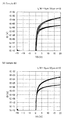
- FIG. 8 shows the electrical characteristics of the transistor according to Example 2.
- the functions of the source and the drain of the transistor may be switched when the polarity of the transistor or the direction of current changes in circuit operation. Therefore, the terms source and drain can be used interchangeably.
- the term “electrically connected” includes the case where they are connected via "something having an electrical function".
- the “thing having an electrical function” is not particularly limited as long as it can transmit and receive electrical signals between connection targets.
- “those having some electrical action” include electrodes, wirings, switching elements such as transistors, resistance elements, inductors, capacitors, elements having various other functions, and the like.
- membrane and the term “layer” can be interchanged with each other.
- conductive layer and “insulating layer” may be interchangeable with the terms “conductive film” and “insulating film” in some cases.
- an off-state current is a drain current when the transistor is in an off state (also referred to as a non-conduction state or a cutoff state) unless otherwise specified.
- an off state in the n-channel transistor, the voltage V gs between the gate and the source is lower than the threshold voltage V th (in the p-channel transistor, higher than V th ) unless otherwise specified.
- a display panel which is one mode of a display device has a function of displaying (outputting) an image or the like on a display surface.
- the display panel is an aspect of the output device.
- a substrate in which a connector such as a flexible printed circuit (FPC) or a TCP (Tape Carrier Package) is attached to a substrate of a display panel, or an IC by a COG (Chip On Glass) method or the like on a substrate What was implemented may be called a display panel module, a display module, or simply a display panel or the like.
- a touch panel which is an aspect of a display device has a function of displaying an image or the like on a display surface, and a touch or touch of a detected object such as a finger or a stylus on the display surface. And a function as a touch sensor to detect. Therefore, the touch panel is an aspect of the input / output device.
- the touch panel can also be called, for example, a display panel with a touch sensor (or a display device) or a display panel with a touch sensor function (or a display device).
- the touch panel can also be configured to have a display panel and a touch sensor panel. Alternatively, the inside or the surface of the display panel may have a function as a touch sensor.
- a touch panel module one in which a connector or an IC is mounted on a substrate of a touch panel may be referred to as a touch panel module, a display module, or simply a touch panel or the like.
- Embodiment 1 the semiconductor device of one embodiment of the present invention, a manufacturing method thereof, and the like will be described.
- One embodiment of the present invention is a gate electrode, a gate insulating layer over the gate electrode, a semiconductor layer over the gate insulating layer, a pair of source electrode and drain electrode in contact with the top surface of the semiconductor layer, over a formation surface.
- a transistor having The semiconductor layer preferably includes a metal oxide exhibiting semiconductor characteristics (hereinafter, also referred to as an oxide semiconductor).
- a low-resistance conductive material containing copper, silver, gold, aluminum, or the like for the source electrode and the drain electrode.
- copper or aluminum is preferable because of its excellent mass productivity.
- the source electrode and the drain electrode are formed by depositing a conductive film so as to cover the semiconductor layer and etching the conductive film so as to be separated on the semiconductor layer. Immediately after the source electrode and the drain electrode are formed, the surface of the channel formation region of the semiconductor layer opposite to the gate electrode (also referred to as the back channel side) is exposed.
- the process for supplying oxygen includes heat treatment in an atmosphere containing oxygen, or plasma treatment in an atmosphere containing oxygen.
- the process of supplying oxygen to the back channel oxidizes the source electrode and the drain electrode, and the conductivity is impaired, etc. May adversely affect the electrical characteristics and reliability of the transistor.
- plasma treatment using a mixed gas of a gas containing oxygen and a gas having reducibility is performed as a process of supplying oxygen to the back channel. This makes it possible to effectively supply oxygen to the back channel while suppressing the oxidation of the source electrode and the drain electrode.
- the semiconductor layer and the source electrode And plasma treatment is performed on the surface of the drain electrode.
- the first gas for example, nitrogen oxides such as N 2 O (nitrogen monoxide or dinitrogen monoxide), NO 2 (nitrogen dioxide), NO (nitrogen monoxide), or O 2 (oxygen), O 3
- a gas containing (ozone) or the like It is preferable to use a gas containing (ozone) or the like.
- the second gas for example, a gas containing NH 3 (ammonia), H 2 (hydrogen) or the like is preferably used.
- a mixed gas containing a rare gas such as Ar in addition to N 2 O and NH 3 as a mixed gas used for plasma processing.
- the ratio of the first gas to the second gas in the mixed gas can be controlled by controlling the flow rates of the respective gases supplied to the plasma processing chamber.
- the ratio of the two gases in the mixed gas can be expressed, for example, by a volume ratio, a partial pressure ratio, or a weight ratio.
- the flow ratio of the two types of gas supplied to the processing chamber substantially corresponds to the volume ratio and partial pressure ratio of the two types of gas.
- the flow rate of the second gas is preferably at least equal to or less than the flow rate of the first gas.
- the amount of hydrogen element supplied to the semiconductor layer can be reduced. This is because, even when the unreacted excess hydrogen element contained in the second gas is present, it reacts with the oxygen element contained in the first gas and is exhausted from the processing chamber in the form of a hydroxide. It is guessed.
- the flow ratio of the second gas is 0.5% to 100%, preferably 1% to 90%. %, More preferably 3% or more and 80% or less, further preferably 3% or more and 60% or less, and further preferably 3% or more and 50% or less.
- the insulating film is preferably formed by plasma enhanced chemical vapor deposition (plasma CVD). At this time, it is preferable that the plasma treatment and the deposition of the insulating film be performed consecutively in the same deposition chamber in the same apparatus. Further, it is preferable to perform the plasma treatment and the film formation of the insulating film at the same temperature.
- plasma CVD plasma enhanced chemical vapor deposition
- a deposition gas at the time of deposition of the insulating film containing an oxide a mixed gas containing a deposition gas containing a silicon element or the like and the first gas used in the plasma treatment is preferably used.
- a mixed gas containing a deposition gas containing a silicon element or the like and the first gas used in the plasma treatment is preferably used.
- the interface between the semiconductor layer and the insulating film can be favorable.
- a silicon oxynitride film can be formed using an N 2 O gas as the first gas and a mixed gas containing this and an SiH 4 (silane) gas as a film forming gas.
- a conductive film containing a metal element different from the above may be stacked on the above-described conductive film containing copper or aluminum.
- a stacked structure of three or more layers may be employed in which a conductive film containing a metal element different from the above is stacked so as to sandwich the conductive film containing copper, aluminum, or the like.
- the conductive film located at the top is a material which is less likely to be bonded to oxygen than a conductive film containing copper or aluminum or the like, or a material whose conductivity is not easily impaired even by oxidation. Is preferred.
- a material in which oxygen in the semiconductor layer does not easily diffuse is preferably used.
- a conductive material containing titanium, tungsten, molybdenum, chromium, tantalum, zinc, indium, platinum, ruthenium, or the like can be used as the conductive film in the uppermost position and the conductive film in contact with the semiconductor layer.
- the semiconductor layer preferably has a stacked structure in which two or more metal oxide films having different crystallinity are stacked.
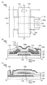
- FIG. 1A is a top view of the transistor 100
- FIG. 1B corresponds to a cross-sectional view of a cross section taken along dashed-dotted line A1-A2 in FIG. 1A
- FIG. 1A corresponds to a cross-sectional view taken along a dashed-dotted line B1-B2 shown in FIG.
- the dashed-dotted line A1-A2 direction corresponds to the channel length direction
- the dashed-dotted line B1-B2 direction corresponds to the channel width direction.
- FIG. 1A some of components of the transistor 100 (a gate insulating layer or the like) are omitted.
- FIG. 1A some of the components are omitted in the drawings as well.
- the transistor 100 is provided over the substrate 102 and includes a conductive layer 104, an insulating layer 106, a semiconductor layer 108, a conductive layer 112a, a conductive layer 112b, and the like.
- An insulating layer 106 is provided to cover the conductive layer 104.
- the semiconductor layer 108 has an island shape and is provided over the insulating layer 106.
- the conductive layer 112 a and the conductive layer 112 b are provided in contact with the top surface of the semiconductor layer 108 and spaced apart from each other on the semiconductor layer 108.
- an insulating layer 114 is provided to cover the insulating layer 106, the conductive layer 112 a, the conductive layer 112 b, and the semiconductor layer 108, and the insulating layer 116 is provided over the insulating layer 114.
- the conductive layer 104 functions as a gate electrode.
- Part of the insulating layer 106 functions as a gate insulating layer.
- the conductive layer 112 a functions as one of a source electrode and a drain electrode, and the conductive layer 112 b functions as the other.
- a region overlapping with the conductive layer 104 of the semiconductor layer 108 functions as a channel formation region.
- the transistor 100 is a so-called bottom gate transistor in which a gate electrode is provided on the formation surface side of the semiconductor layer 108.
- the surface of the semiconductor layer 108 opposite to the conductive layer 104 may be referred to as a back channel surface.
- the transistor 100 is a transistor with a so-called channel etch structure, which does not have a protective layer between the back channel side of the semiconductor layer 108 and the source and drain electrodes.
- the semiconductor layer 108 has a stacked structure in which a semiconductor layer 108 a and a semiconductor layer 108 b are sequentially stacked from the formation surface side (the substrate 102 side). It is preferable that the semiconductor layer 108 a and the semiconductor layer 108 b both contain a metal oxide.
- the semiconductor layer 108 b located on the back channel side is preferably a film having higher crystallinity than the semiconductor layer 108 a located on the conductive layer 104 side. Accordingly, when the conductive layer 112 a and the conductive layer 112 b are processed, part of the semiconductor layer 108 can be prevented from being etched and disappearing.
- the semiconductor layer 108 is made of indium, M (M is gallium, aluminum, silicon, boron, yttrium, tin, copper, vanadium, beryllium, titanium, iron, nickel, germanium, zirconium, molybdenum, lanthanum, cerium, neodymium, It is preferable to have zinc and one or more selected from hafnium, tantalum, tungsten, or magnesium.
- M is preferably aluminum, gallium, yttrium or tin.
- an oxide containing indium, gallium, and zinc is preferably used as the semiconductor layer 108.
- the semiconductor layer 108 a and the semiconductor layer 108 b may be layers different in composition, different in crystallinity, or different in impurity concentration. In addition, a stacked structure of three or more layers may be used.
- the conductive layer 112a and the conductive layer 112b have a stacked structure in which the conductive layer 113a, the conductive layer 113b, and the conductive layer 113c are stacked in this order from the formation surface side.
- the conductive layer 113 b is preferably formed using a low-resistance conductive material containing copper, silver, gold, aluminum, or the like.
- the conductive layer 113 b preferably contains copper or aluminum.
- the conductive layer 113 b is preferably formed using a conductive material which has lower resistance than the conductive layer 113 a and the conductive layer 113 c. Thus, the conductive layer 112 a and the conductive layer 112 b can have extremely low resistance.
- the conductive layers 113a and 113c can each independently be formed using a conductive material different from the conductive layer 113b.
- a conductive material preferably containing titanium, tungsten, molybdenum, chromium, tantalum, zinc, indium, platinum, ruthenium, or the like is preferably used.
- the oxidation of the surface of the conductive layer 113b can be suppressed, or the element of the conductive layer 113b is a peripheral layer. Diffusion can be suppressed.
- the metal element contained in the conductive layer 113a can be prevented from diffusing into the semiconductor layer 108, so that the transistor 100 can have high reliability. realizable.
- the insulating layer 114 is provided in contact with the end portion of the conductive layer 113 b.
- the conductive layer 113 b is a conductive material that is easily oxidized and the insulating layer 114 including an oxide film is formed thereon, the conductive layer 113 b Can suppress the surface oxidation of Therefore, it is one of the features of one embodiment of the present invention that a different layer including an oxide or the like is not observed at the interface between the conductive layer 113 b and the insulating layer 114.
- the structures of the conductive layer 112 a and the conductive layer 112 b are not limited to a three-layer structure, and may have a two-layer structure or a four-layer structure including a conductive layer containing copper, silver, gold, or aluminum.
- a two-layer structure in which the conductive layer 113a and the conductive layer 113b are stacked may be used, or a two-layer structure in which the conductive layer 113b and the conductive layer 113c may be stacked may be used.
- any of the above-described conductive materials which can be used for the conductive layer 113a and the conductive layer 113b can be used as appropriate.
- an insulating material containing an oxide is preferably used for the insulating layer 106 and the insulating layer 114 which are in contact with the semiconductor layer 108.
- an insulating material containing an oxide is used for a layer in contact with the semiconductor layer 108.
- a nitride insulating film such as silicon nitride or aluminum nitride may be used for the insulating layer 106.
- oxygen it is preferable to apply oxygen to the top of the insulating layer 106 to form a region containing oxygen.
- the treatment for adding oxygen include heat treatment or plasma treatment in an atmosphere containing oxygen, and ion doping treatment.
- the insulating layer 116 functions as a protective layer which protects the transistor 100.
- an inorganic insulating material such as silicon nitride, silicon nitride oxide, silicon oxide, silicon oxynitride, aluminum oxide, or aluminum nitride can be used.
- a material which hardly diffuses oxygen such as silicon nitride or aluminum oxide, as the insulating layer 116, oxygen from the semiconductor layer 108 or the insulating layer 114 to the outside through the insulating layer 116 due to heat applied during the manufacturing process. Is preferable because it can prevent the detachment of the
- an organic insulating material which functions as a planarization film may be used as the insulating layer 116.
- a stacked film of a film containing an inorganic insulating material and a film containing an organic insulating material may be used as the insulating layer 116.
- the semiconductor layer 108 may be located in a portion in contact with the conductive layer 112 a and the conductive layer 112 b and in the vicinity thereof, and a pair of low-resistance regions functioning as a source region and a drain region may be formed.
- the region is a part of the semiconductor layer 108 and has a lower resistance than the channel formation region.
- the low resistance region can be rephrased as a region where the carrier density is high, a region which is n-type, or the like.
- a region which is sandwiched between the pair of low-resistance regions and overlaps with the conductive layer 104 functions as a channel formation region.
- FIG. 2A is a top view of the transistor 100A
- FIG. 2B is a cross-sectional view in the channel length direction of the transistor 100B
- FIG. 2C is a cross-sectional view in the channel width direction.
- the transistor 100A is mainly different from Structural Example 1 in that the conductive layer 120a and the conductive layer 120b are provided over the insulating layer 116.
- the conductive layer 120 a has a region overlapping with the semiconductor layer 108 with the insulating layer 116 and the insulating layer 114 interposed therebetween.
- the conductive layer 104 has a function as a first gate electrode (also referred to as a bottom gate electrode), and the conductive layer 120a has a function as a second gate electrode (also referred to as a top gate electrode).
- part of the insulating layer 116 and the insulating layer 114 functions as a second gate insulating layer.
- the conductive layer 120a is electrically connected to the conductive layer 104 through the opening 142b provided in the insulating layer 116, the insulating layer 114, and the insulating layer 106. It may be connected to Accordingly, the same potential can be applied to the conductive layer 120a and the conductive layer 104, and a transistor with high on-state current can be realized.
- the conductive layer 104 and the conductive layer 120 a preferably protrude outward beyond the end portion of the semiconductor layer 108 in the channel width direction. At this time, as shown in FIG. 2C, the whole of the semiconductor layer 108 in the channel width direction is covered with the conductive layer 104 and the conductive layer 120 a.
- the semiconductor layer 108 can be electrically surrounded by an electric field generated by the pair of gate electrodes.
- the same potential is preferably applied to the conductive layer 104 and the conductive layer 120 a. Accordingly, an electric field for inducing a channel can be effectively applied to the semiconductor layer 108, so that the on-state current of the transistor 100A can be increased. Therefore, the transistor 100A can be miniaturized.
- the conductive layer 104 and the conductive layer 120 a may not be connected. At this time, a constant potential may be supplied to one of the pair of gate electrodes, and a signal for driving the transistor 100A may be supplied to the other. At this time, the threshold voltage in driving the transistor 100A with the other electrode can be controlled by the potential supplied to the one electrode.
- the conductive layer 120 b is electrically connected to the conductive layer 112 b through an opening 142 a provided in the insulating layer 116 and the insulating layer 114.
- the conductive layer 120 b can be used as a wiring or an electrode.
- the conductive layer 120 b can function as a pixel electrode or a wiring for connecting to the pixel electrode.
- thin films insulating films, semiconductor films, conductive films, and the like that constitute a semiconductor device are formed by sputtering, chemical vapor deposition (CVD), vacuum evaporation, pulse laser deposition (PLD: Pulse Laser Deposition). ), Atomic layer deposition (ALD), or the like.
- CVD chemical vapor deposition
- PLA Pulse Laser Deposition
- ALD Atomic layer deposition
- CVD method include plasma enhanced chemical vapor deposition (PECVD), thermal CVD and the like.
- PECVD plasma enhanced chemical vapor deposition
- MOCVD metal organic chemical vapor deposition
- thin films (insulating films, semiconductor films, conductive films, etc.) constituting a semiconductor device can be spin-coated, dip, spray-coated, inkjet, dispensing, screen printing, offset printing, doctor knife, slit coat, roll coat, curtain coat , Knife coating or the like.
- the thin film when processing a thin film forming the semiconductor device, can be processed using a photolithography method or the like.
- the thin film may be processed by a nanoimprint method, a sand blast method, a lift-off method or the like.
- the island-shaped thin film may be formed directly by a film formation method using a shielding mask such as a metal mask.
- the photolithography method there are typically the following two methods.
- One is a method of forming a resist mask on a thin film to be processed, processing the thin film by etching or the like, and removing the resist mask.
- the other is a method of processing the thin film into a desired shape by forming a thin film having photosensitivity, followed by exposure and development.
- light used for exposure may be, for example, i-ray (wavelength 365 nm), g-ray (wavelength 436 nm), h-ray (wavelength 405 nm), or a mixture of these.
- ultraviolet light, KrF laser light, ArF laser light or the like can also be used.
- the exposure may be performed by the immersion exposure technique.
- extreme ultraviolet (EUV: Extreme Ultra-violet) or X-rays may be used.
- an electron beam can be used instead of light used for exposure. The use of extreme ultraviolet light, X-rays or electron beams is preferable because extremely fine processing is possible. In the case where exposure is performed by scanning a beam such as an electron beam, a photomask is not necessary.
- etching of the thin film a dry etching method, a wet etching method, a sand blast method, or the like can be used.
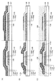
- FIGS. 3 to 6 are views for explaining a method of manufacturing the transistor 100A.
- the cross section in the channel length direction is shown on the left side
- the cross section in the channel width direction is shown on the right side.
- a conductive film is formed over the substrate 102, a resist mask is formed over the conductive film by a lithography process, and then the conductive film is etched to form a conductive layer 104 which functions as a gate electrode.
- an insulating layer 106 covering the conductive layer 104 and the substrate 102 is formed (FIG. 3A).
- the insulating layer 106 can be formed by, for example, a PECVD method.
- oxygen may be supplied to the insulating layer 106.
- oxygen supply processing oxygen radicals, oxygen atoms, oxygen atom ions, oxygen molecular ions, or the like are supplied to the insulating layer 106 by an ion doping method, an ion implantation method, plasma treatment, or the like.
- oxygen may be added to the insulating layer 106 through the film. The membrane is preferably removed after the addition of oxygen.
- a conductive film or a semiconductor film containing one or more of indium, zinc, gallium, tin, aluminum, chromium, tantalum, titanium, molybdenum, nickel, iron, cobalt, or tungsten is used as the film which suppresses the above-described desorption of oxygen. be able to.
- heat treatment may be performed to remove water or hydrogen from the surface and the film of the insulating layer 106 before the process of supplying oxygen.
- heat treatment can be performed at a temperature higher than or equal to 300 ° C and lower than the heat resistance temperature of the conductive layer 104, preferably, higher than or equal to 300 ° C and lower than or equal to 450 ° C in a nitrogen atmosphere.
- the metal oxide film 108af and the metal oxide film 108bf are each preferably formed by a sputtering method using a metal oxide target.
- an inert gas eg, helium gas, argon gas, xenon gas, or the like
- oxygen flow ratio the ratio of oxygen gas to the entire film forming gas at the time of forming the metal oxide film
- a metal oxide film with high conductivity By reducing the oxygen flow rate ratio and forming a metal oxide film with relatively low crystallinity, a metal oxide film with high conductivity can be obtained. On the other hand, by setting the oxygen flow ratio high and using a metal oxide film having relatively high crystallinity, a metal oxide film having high etching resistance and being electrically stable can be obtained.
- the metal oxide film 108af located on the side of the conductive layer 104 which functions as a gate electrode is a film with low crystallinity
- the metal oxide film 108bf located on the back channel side is a film with low crystallinity.
- the substrate temperature may be higher than or equal to room temperature and 200 ° C. or lower, preferably, the substrate temperature may be higher than or equal to room temperature and 140 ° C or lower.
- productivity is preferably high.
- the oxygen flow ratio at the time of film formation of the metal oxide film 108af is 0% or more and less than 50%, preferably 0% or more and 30% or less, more preferably 0% or more and 20% or less, typically Is 10%.
- the oxygen flow ratio at the time of film formation of the metal oxide film 108bf is 50% to 100%, preferably 60% to 100%, more preferably 80% to 100%, and still more preferably 90% to 100%. Hereinafter, it is typically 100%.
- conditions such as pressure, temperature, and power at the time of film formation may be different between the metal oxide film 108af and the metal oxide film 108bf, the conditions are the same except for the oxygen flow ratio. It is preferable because the time required for the membrane process can be shortened.
- the metal oxide film 108af and the metal oxide film 108bf may have different compositions.
- the In content in the metal oxide film 108bf is higher than that of the metal oxide film 108af. It is preferred to use an oxide target.
- a resist mask is formed on the metal oxide film 108bf, and the metal oxide film 108af and the metal oxide film 108bf are processed by etching, and then the resist mask is formed.
- the semiconductor layer 108 By removing the semiconductor layer 108, an island-shaped semiconductor layer 108 in which the semiconductor layer 108a and the semiconductor layer 108b are stacked can be formed (FIG. 3C).
- a conductive film 113af, a conductive film 113bf, and a conductive film 113cf are stacked and formed so as to cover the insulating layer 106 and the semiconductor layer 108 (FIG. 4A).
- the conductive film 113 b f is a film to be the conductive layer 113 b later, and preferably contains copper, silver, gold, or aluminum.
- the conductive film 113 af and the conductive film 113 cf are films to be later formed to be the conductive layer 113 a and the conductive layer 113 b, and each of them independently contains titanium, tungsten, molybdenum, chromium, tantalum, zinc, indium, platinum, ruthenium, or the like. Is preferred.
- the conductive film 113af, the conductive film 113bf, and the conductive film 113cf are preferably formed using a film formation method such as a sputtering method, an evaporation method, or a plating method.
- a resist mask is formed over the conductive film 113cf, and the conductive film 113cf, the conductive film 113bf, and the conductive film 113af are etched to form a stacked structure of the conductive layer 113a, the conductive layer 113b, and the conductive layer 113c.
- the conductive layer 112a and the conductive layer 112b can be formed (FIG. 4B).
- the conductive layer 112 a and the conductive layer 112 b are preferably processed so as to be separated over the channel formation region of the semiconductor layer 108 as illustrated in FIG. 4B. In other words, it is preferable that processing is performed so that opposing ends of the conductive layer 112 a and the conductive layer 112 b overlap with both the conductive layer 104 and the semiconductor layer 108. Thus, the on current of the transistor can be increased.
- the conductive film 113cf, the conductive film 113bf, and the conductive film 113af can be etched by wet etching, dry etching, or the like.
- the three layers may be etched at once in one step, or may be sequentially etched in different steps.
- Plasma treatment is performed in a mixed gas atmosphere of a gas containing oxygen and a reducing gas, and oxygen is supplied to the semiconductor layer 108 from the back channel side.
- FIG. 4C a state in which the surfaces of the semiconductor layer 108, the conductive layer 112a, and the insulating layer 106 are exposed to the plasma 130 is schematically shown.
- the mixed gas it is preferable to use a mixed gas of a first gas containing an oxygen element and not containing a hydrogen element and a second gas containing a hydrogen element and not containing an oxygen element.
- a first gas having oxidizing properties for example, nitrogen oxides such as N 2 O (nitrous oxide or dinitrogen monoxide), NO 2 (nitrogen dioxide), NO (nitrogen monoxide), O 2 (oxygen)
- a gas containing or or O 3 (ozone) a gas containing or or O 3 (ozone).
- a gas containing NH 3 (ammonia) or H 2 (hydrogen) is preferably used.
- a mixed gas containing N 2 O, NH 3 , and a rare gas is preferably used as a mixed gas used for plasma treatment.
- Ar etc. are mentioned, for example.
- the ratio of the first gas to the second gas in the mixed gas can be adjusted by controlling the flow rate when supplied to the processing chamber of plasma processing.
- the flow ratio of the first gas to the second gas in the mixed gas can be set according to the easiness of oxidation of the conductive layer 113a, the conductive layer 113b, and the conductive layer 113c, but at least the second gas It is preferable to set the flow rate of H.sub.2 to the flow rate of the first gas or less.
- the flow rate of the second gas with respect to the flow rate of the first gas is too small, oxidation of the surface of the conductive layer 113b or the like becomes dominant, and an oxide is easily formed on the surface.
- the flow rate of the second gas with respect to the flow rate of the first gas is too large, the surface of the semiconductor layer 108 may be reduced or hydrogen may be supplied to the semiconductor layer 108.
- the flow rate of the second gas is 0.5% to 100%, preferably 1% to 90%, more preferably 3% to 80%. More preferably, it can be 3% or more and 60% or less, more preferably 3% or more and 50% or less.
- FIG. 5A shows an enlarged view of an end portion of the conductive layer 113a, the conductive layer 113b, and the conductive layer 113c which constitute the conductive layer 112a over the semiconductor layer 108 in FIG. 4C, and the vicinity thereof.
- activated oxygen radicals, oxygen atoms, oxygen atom ions, molecular oxygen ions, and the like are supplied to the semiconductor layer 108 b.
- FIG. 5B shows an example in the case where the gas used for plasma treatment does not contain a reducing gas.
- the oxide 113bo is formed on part of the conductive layer 113b exposed to the plasma 130a.
- an oxide is also formed on the surface.
- the oxide 113bo and the like formed on the surface of the conductive layer 113b partially scatter during the plasma treatment or at the time of forming the insulating layer 114 later, thereby contaminating the surface of the semiconductor layer 108b. There is a case.
- An oxide attached to the semiconductor layer 108 b can function as a donor or an acceptor, which might adversely affect the electrical characteristics and reliability of the transistor.
- the copper element may function as a carrier trap, which may impair the electrical characteristics and reliability of the transistor.
- the insulating layer 114 is formed to cover the conductive layer 112 a, the conductive layer 112 b, the semiconductor layer 108, and the insulating layer 106.
- the insulating layer 114 is preferably formed, for example, in an atmosphere containing oxygen.
- the film is preferably formed by plasma CVD in an atmosphere containing oxygen.
- the insulating layer 114 with few defects can be obtained.
- an oxide film such as a silicon oxide film or a silicon oxynitride film is preferably formed using a plasma-enhanced chemical vapor deposition apparatus (referred to as a PECVD apparatus or simply referred to as a plasma CVD apparatus).
- a plasma-enhanced chemical vapor deposition apparatus referred to as a PECVD apparatus or simply referred to as a plasma CVD apparatus.
- the source gas it is preferable to use a deposition gas containing silicon and an oxidizing gas.
- the deposition gas containing silicon include silane, disilane, trisilane, fluorosilane and the like.
- the oxidizing gas include oxygen, ozone, dinitrogen monoxide, and nitrogen dioxide.
- the insulating layer 114 PECVD in which the flow rate of the oxidizing gas is larger than 20 times and less than 100 times, or 40 times to 80 times that of the deposition gas, and the pressure in the processing chamber is less than 100 Pa or 50 Pa or less.
- the insulating layer 114 may be formed by PECVD using microwaves.
- Microwave refers to the frequency range of 300 MHz to 300 GHz.
- the microwave has a low electron temperature and a small electron energy.
- the rate used for accelerating electrons is small, and it can be used for dissociation and ionization of more molecules, and can excite high density plasma (high density plasma) . Therefore, the insulating layer 114 with few defects can be formed with less plasma damage to the deposition surface and the deposit.
- the plasma treatment is preferably performed by a deposition apparatus for the insulating layer 114.
- plasma treatment is preferably performed in a deposition chamber in which the insulating layer 114 is deposited.
- the film may be transferred to the film formation chamber of the insulating layer 114 under reduced pressure without being exposed to the air.
- the plasma treatment and the deposition of the insulating layer 114 are preferably performed at the same temperature.
- a deposition gas at the time of deposition of the insulating layer 114 containing an oxide a mixed gas containing an oxidizing first gas used in plasma treatment and a deposition gas containing a silicon element or the like is used. Is preferred.
- the interface between the semiconductor layer and the insulating film can be favorable.
- a silicon oxynitride film can be formed using an N 2 O gas as the first gas and a mixed gas containing this and an SiH 4 (silane) gas as a film forming gas.
- oxygen may be supplied to the insulating layer 114.
- the process for supplying oxygen can be performed by a method similar to that of the insulating layer 106.
- the insulating layer 116 is formed so as to cover the insulating layer 114 (FIG. 6A).
- an insulating film in which oxygen, hydrogen, water, and the like are less likely to be diffused than the insulating layer 114 is preferably used. Since the insulating layer 116 hardly diffuses oxygen, the oxygen in the semiconductor layer 108 can be prevented from being released to the outside through the insulating layer 114. In addition, since the insulating layer 116 hardly diffuses hydrogen, diffusion of hydrogen, water, and the like from the outside to the semiconductor layer 108 and the like can be prevented.
- a conductive film is formed to cover the opening 142a and the opening 142b, and the conductive film is processed to form the conductive layer 120a and the conductive layer 120b (FIG. 6 (B )).
- the transistor 100A can be manufactured.
- treatment for supplying oxygen to the back channel of the semiconductor layer can be performed while suppressing oxidation of the source electrode and the drain electrode, so that favorable electrical characteristics and high reliability can be obtained. Can be manufactured.
- the transistor 100B illustrated in FIGS. 7A and 7B is different from the transistor 100 described in Structural Example 1 mainly in that the semiconductor layer 108 does not have a stacked-layer structure.
- the manufacturing process can be simplified and productivity can be improved.
- a metal oxide film having crystallinity is preferably used as the semiconductor layer 108.
- the transistor 100C illustrated in FIGS. 7C and 7D is mainly the transistor illustrated in the above configuration example 1 in that not only the semiconductor layer 108 but also the conductive layer 112a and the conductive layer 112b have a stacked-layer structure. It is different from 100.
- Productivity can be further improved by forming the conductive layer 112 a and the conductive layer 112 b into a single-layer structure in addition to the semiconductor layer 108.
- a conductive material containing copper, silver, gold, or aluminum is preferably used as the conductive layer 112a and the conductive layer 112b. According to the manufacturing method of one embodiment of the present invention, oxidation of the conductive layer 112a and the conductive layer 112b can be suppressed in the treatment of supplying oxygen to the semiconductor layer 108; thus, the conductive layer containing copper or the like in this manner can be a single layer. Even when used, a highly reliable transistor can be realized.
- a transistor 100D illustrated in FIGS. 8A, 8B, and 8C is mainly different from the transistor 100A illustrated in the above configuration example 2 in that the positions of the conductive layer 120a and the conductive layer 120b are different.
- the conductive layer 120 a and the conductive layer 120 b are located between the insulating layer 114 and the insulating layer 116.
- the conductive layer 120 b is electrically connected to the conductive layer 112 b through an opening 142 a provided in the insulating layer 114.
- the distance between the conductive layer 120a and the semiconductor layer 108 can be reduced, whereby the electrical characteristics of the transistor 100D can be improved.
- the transistor 100E illustrated in FIGS. 9A, 9B, and 9C is mainly different from the transistor 100 illustrated in the above configuration example 1 in that the configuration of the insulating layer 114 is different.
- the insulating layer 114 is processed into an island shape covering the channel formation region of the semiconductor layer 108. Further, end portions of the conductive layer 112 a and the conductive layer 112 b located on the semiconductor layer 108 are located on the insulating layer 114. Accordingly, the insulating layer 114 functions as a so-called channel protective layer, and can protect the back channel side of the semiconductor layer 108 when the conductive layer 112 a and the conductive layer 112 b are etched.
- plasma treatment is performed by the above-described method to suppress oxidation of the conductive layer 112a and the conductive layer 112b, and to suppress the oxidation in the insulating layer 114 and the insulating layer 114.
- Oxygen can be supplied to the semiconductor layer 108 through the through holes. Further, oxygen in the insulating layer 114 may be supplied to the semiconductor layer 108 by heat treatment after plasma treatment.
- the transistor 100F illustrated in FIGS. 10A, 10B, and 10C is mainly different from the transistor 100E illustrated in the modification 4 in that the configuration of the insulating layer 114 is different.
- the insulating layer 114 is provided to cover the semiconductor layer 108, the insulating layer 106, and the like. In the insulating layer 114, an opening 142c is provided in a portion where the semiconductor layer 108 and the conductive layer 112a or the conductive layer 112b are connected.
- FIG. 11 is a schematic top view showing a part of the sub-pixel of the display device.
- One sub-pixel includes at least one transistor and a conductive layer (here, the conductive layer 120b) functioning as a pixel electrode.
- the conductive layer 120b functioning as a pixel electrode.
- other transistors may be used depending on the type of display element applied to the sub-pixel, the function to be added to the pixel, etc.
- a capacitor or the like can be provided as appropriate.
- part of the conductive layer 104 functions as a gate line (also referred to as a scanning line), and part of the conductive layer 112 a functions as a source line (also referred to as a video signal line).
- a part functions as a wiring which electrically connects the transistor and the conductive layer 120 b.
- the conductive layer 104 has a top surface shape in which a portion protrudes, and the semiconductor layer 108 is provided over the protruding portion to form a transistor.
- FIGS. 11B and 11C each show an example where the conductive layer 104 does not have a protruding portion.
- FIG. 11B is an example in which the channel length direction of the semiconductor layer 108 and the extension direction of the conductive layer 104 are parallel, and
- FIG. 11C is an example in which these are orthogonal to each other.
- the conductive layer 112b has a U-shaped upper surface shape having a substantially arc-shaped portion.
- the conductive layer 112 a and the conductive layer 112 b are arranged on the semiconductor layer 108 such that the two distances are always equal. With such a structure, the channel width of the transistor can be increased, and a larger current can flow.
- the transistor of one embodiment of the present invention can be applied to a variety of circuits and devices as well as a display device.
- various circuits in an IC chip such as an arithmetic circuit, a memory circuit, a driver circuit, an interface circuit, and the like mounted on an electronic device or the like, or a display device to which a liquid crystal element or an organic EL element is applied, a touch sensor, an optical It can be suitably used as a drive circuit or the like in various sensor devices such as a sensor and a biological sensor.
- the material of the substrate 102 and the like are not particularly limited, but at least the heat resistance needs to be able to withstand the heat treatment to be performed later.
- a single crystal semiconductor substrate made of silicon or silicon carbide, a polycrystalline semiconductor substrate, a compound semiconductor substrate such as silicon germanium, an SOI substrate, a glass substrate, a ceramic substrate, a quartz substrate, a sapphire substrate or the like is used as the substrate 102. It is also good.
- a substrate provided with a semiconductor element over these substrates may be used as the substrate 102.
- a flexible substrate may be used as the substrate 102, and the transistor 100 and the like may be formed directly on the flexible substrate.
- a peeling layer may be provided between the substrate 102 and the transistor 100 or the like. The release layer can be used for separation from the substrate 102 and reprinting onto another substrate after a semiconductor device is partially or entirely completed thereon. At that time, the transistor 100 and the like can be transferred to a substrate with low heat resistance or a flexible substrate.
- an oxide insulating film or a nitride insulating film can be formed in a single layer or stacked layers. Note that in order to improve interface characteristics with the semiconductor layer 108, at least a region of the insulating layer 106 in contact with the semiconductor layer 108 is preferably formed using an oxide insulating film. Further, for the insulating layer 106, a film which releases oxygen by heating is preferably used.
- the insulating layer 106 for example, silicon oxide, silicon oxynitride, silicon nitride oxide, silicon nitride, aluminum oxide, hafnium oxide, gallium oxide, Ga-Zn oxide, or the like may be used, and it can be provided as a single layer or a stack.
- the surface in contact with the semiconductor layer 108 is subjected to pretreatment such as oxygen plasma treatment; Preferably, or near the surface is oxidized.
- Conductivity of a semiconductor device such as a conductive layer 104 functioning as a gate electrode and a conductive layer 120a, a wiring 120b functioning as a wiring, a conductive layer 112a functioning as one of a source electrode or a drain electrode, and a conductive layer 112b functioning as the other
- the film may be a metal element selected from chromium, copper, aluminum, gold, silver, zinc, molybdenum, tantalum, titanium, tungsten, manganese, nickel, iron, cobalt, or an alloy containing the aforementioned metal element, It can form each using the alloy etc. which combined the metallic element mentioned above.
- a low-resistance conductive material containing copper, silver, gold, aluminum, or the like is preferably used as the conductive layer 112 a functioning as one of the source electrode and the drain electrode and the conductive layer 112 b functioning as the other.
- a low-resistance conductive material containing copper, silver, gold, aluminum, or the like is preferably used as the conductive layer 112 a functioning as one of the source electrode and the drain electrode and the conductive layer 112 b functioning as the other.
- copper or aluminum is preferable because of its excellent mass productivity.
- In-Sn oxide, In-W oxide, In-W-Zn oxide, In-Ti oxide, In-Ti-Sn oxide, In-Zn oxide And oxide conductors such as In-Sn-Si oxide and In-Ga-Zn oxide, or metal oxide films can also be applied.
- oxide conductor Oxide Conductor
- OC Oxide Conductor
- a donor level is formed in the vicinity of the conduction band.
- the metal oxide becomes highly conductive and becomes conductive.
- a conductive metal oxide can be referred to as an oxide conductor.
- a stacked structure of a conductive film containing the oxide conductor (a metal oxide) and a conductive film containing a metal or an alloy may be used as the conductive film included in the semiconductor device.
- the wiring resistance can be reduced by using a conductive film containing a metal or an alloy.
- a conductive film including an oxide conductor is preferably applied to the side in contact with the insulating layer which functions as a gate insulating film.
- a Cu-X alloy film (X is Mn, Ni, Cr, Fe, Co, Mo, Ta, or Ti) may be applied to the conductive layer 104, the conductive layer 112a, and the conductive layer 112b.
- X is Mn, Ni, Cr, Fe, Co, Mo, Ta, or Ti
- processing can be performed by a wet etching process, which makes it possible to suppress the manufacturing cost.
- Insulating layer 114 As the insulating layer 114 provided over the semiconductor layer 108, a silicon oxide film, a silicon oxynitride film, an aluminum oxide film, a hafnium oxide film, a yttrium oxide film, or a zirconium oxide film formed by a PECVD method, a sputtering method, an ALD method or the like.
- An insulating layer containing one or more of a film, a gallium oxide film, a tantalum oxide film, a magnesium oxide film, a lanthanum oxide film, a cerium oxide film, a neodymium oxide film, and the like can be used.
- a silicon oxide film or a silicon oxynitride film formed by a plasma CVD method is preferably used.
- the insulating layer 114 may have a stacked structure of two or more layers.
- the sputtering target used to form the In-M-Zn oxide preferably has an atomic ratio of In greater than or equal to an atomic ratio of M.
- the atomic ratio of the semiconductor layer 108 to be formed includes a variation of plus or minus 40% of the atomic ratio of the metal element contained in the above sputtering target.
- the semiconductor layer 108 has an energy gap of 2 eV or more, preferably 2.5 eV or more.
- the off-state current of the transistor can be reduced.
- the semiconductor layer 108 preferably has a non-single-crystal structure.
- the non-single crystal structure includes, for example, a CAAC structure, a polycrystalline structure, a microcrystalline structure, or an amorphous structure described later.
- the amorphous structure has the highest density of defect states
- the CAAC structure has the lowest density of defect states.
- CAAC c-axis aligned crystal
- the CAAC structure is one of crystal structures such as a thin film having a plurality of nanocrystals (crystal regions having a maximum diameter of less than 10 nm), and each nanocrystal has c axis oriented in a specific direction and an a axis And b axes are crystal structures having a feature that nanocrystals are continuously connected without forming grain boundaries without having orientation.
- a thin film having a CAAC structure is characterized in that the c-axis of each nanocrystal is easily oriented in the thickness direction of the thin film, the normal direction of the formation surface, or the normal direction of the surface of the thin film.
- CAAC-OS Oxide Semiconductor
- CAAC-OS is an oxide semiconductor with high crystallinity.
- CAAC-OS can not confirm clear crystal grain boundaries, so that it can be said that the decrease in electron mobility due to crystal grain boundaries does not easily occur.
- the crystallinity of the oxide semiconductor may be lowered due to the mixing of impurities, generation of defects, or the like, so that the CAAC-OS can also be said to be an oxide semiconductor with few impurities or defects (such as oxygen vacancies). Therefore, the oxide semiconductor having a CAAC-OS has stable physical properties. Therefore, an oxide semiconductor having a CAAC-OS is resistant to heat and has high reliability.
- crystallography it is general to take a unit cell with c-axis as a specific axis with respect to three axes (crystal axes) of a-axis, b-axis, and c-axis constituting the unit cell.
- crystal axes three axes
- b-axis a axis
- c-axis constituting the unit cell.
- two axes parallel to the plane direction of the layer are the a axis and b axis
- an axis intersecting the layer is the c axis.
- a typical example of a crystal having such a layered structure is graphite classified into a hexagonal system, and the a-axis and b-axis of the unit cell are parallel to the cleavage plane and the c-axis is orthogonal to the cleavage plane Do.
- a crystal of InGaZnO 4 having a layered crystal structure of YbFe 2 O 4 type can be classified into a hexagonal system, and the a-axis and b-axis of the unit cell are parallel to the plane direction of the layer and c-axis Is orthogonal to the layers (ie, the a and b axes).
- a metal oxide formed by sputtering at a substrate temperature of 100 ° C. to 130 ° C. using the above target has a crystal structure of any one of nc (nano crystal) structure and CAAC structure, or a structure in which these are mixed.
- nc nano crystal
- CAAC room temperature
- a metal oxide formed by a sputtering method with a substrate temperature of room temperature (RT) tends to have a nc crystal structure.
- the room temperature (R.T.) referred to here includes the temperature when the substrate is not intentionally heated.
- This embodiment can be implemented in appropriate combination with at least a part of the other embodiments described in this specification.
- the display device 700 includes a first substrate 701 and a second substrate 705 which are attached by a sealant 712. In the region sealed with the first substrate 701, the second substrate 705, and the sealant 712, the pixel portion 702, the source driver circuit portion 704, and the gate driver circuit portion 706 are provided over the first substrate 701. Be The pixel portion 702 is provided with a plurality of display elements.
- an FPC terminal portion 708 to which an FPC 716 (FPC: Flexible Printed Circuit) is connected is provided in a portion of the first substrate 701 which does not overlap with the second substrate 705.
- FPC 716 Flexible Printed Circuit
- Various signals and the like are supplied to the pixel portion 702, the source driver circuit portion 704, and the gate driver circuit portion 706 through the FPC terminal portion 708 and the signal line 710 by the FPC 716.
- a plurality of gate driver circuit units 706 may be provided.
- the gate driver circuit unit 706 and the source driver circuit unit 704 may be separately formed on a semiconductor substrate or the like and may be in the form of an IC chip packaged.
- the IC chip can be mounted over the first substrate 701 or the FPC 716.
- the transistor which is the semiconductor device of one embodiment of the present invention can be applied to the transistors included in the pixel portion 702, the source driver circuit portion 704, and the gate driver circuit portion 706.
- a liquid crystal element, a light emitting element, or the like can be given.
- a transmissive liquid crystal element, a reflective liquid crystal element, a semi-transmissive liquid crystal element, or the like can be used.
- a light emitting element self-luminous light emitting elements, such as LED (Light Emitting Diode), OLED (Organic LED), QLED (Quantum-dot LED), a semiconductor laser, are mentioned.
- a shutter type or a light interference type MEMS (Micro Electro Mechanical Systems) element a display element to which a microcapsule type, an electrophoresis type, an electrowetting type, an electronic powder fluid (registered trademark) type, or the like is applied is used. It can also be done.
- MEMS Micro Electro Mechanical Systems
- a display device 700A illustrated in FIG. 12B is an example of a display device in which a flexible resin layer 743 is applied instead of the first substrate 701 and the flexible substrate can be used.
- the pixel portion 702 does not have a rectangular shape, and the corner portion has an arc shape.
- the pair of gate driver circuit portions 706 is provided on both sides of the pixel portion 702.
- the gate driver circuit portion 706 is provided along the arc-shaped contour at the corner of the pixel portion 702.
- the resin layer 743 has a shape in which a portion provided with the FPC terminal portion 708 protrudes. Further, a portion of the resin layer 743 including the FPC terminal portion 708 can be folded back on the region P2 in FIG. 12B. By folding back part of the resin layer 743, the display device 700A can be mounted on an electronic device in a state where the FPC 716 is stacked on the back side of the pixel portion 702, and space saving of the electronic device can be achieved. .
- An IC 717 is mounted on the FPC 716 connected to the display device 700A.
- the IC 717 has a function as a source driver circuit, for example.
- the source driver circuit portion 704 in the display device 700A can include at least one of a protective circuit, a buffer circuit, a demultiplexer circuit, and the like.
- a display device 700B illustrated in FIG. 12C is a display device which can be suitably used for an electronic device having a large screen.
- it can be suitably used for a television device, a monitor device, a personal computer (including a notebook type or desktop type), a tablet terminal, digital signage, and the like.
- the display device 700 ⁇ / b> B includes a plurality of source driver ICs 721 and a pair of gate driver circuit portions 722.
- the plurality of source driver ICs 721 are attached to the FPC 723 respectively.
- one terminal is connected to the first substrate 701, and the other terminal is connected to the printed substrate 724.
- the printed substrate 724 can be provided on the back side of the pixel portion 702 and mounted on the electronic device, and space saving of the electronic device can be achieved.
- the gate driver circuit portion 722 is formed on the first substrate 701. Thereby, an electronic device with a narrow frame can be realized.
- a large-sized and high-resolution display device can be realized.
- the present invention can also be applied to a display having a screen size of 30 inches or more, 40 inches, 50 inches, or 60 inches or more.
- a display device with extremely high resolution such as 4K2K or 8K4K can be realized.
- FIGS. 13 to 15 are cross-sectional views taken along the alternate long and short dash line Q-R shown in FIG. 12A.
- FIG. 16 is a cross-sectional view along dashed-dotted line S-T in the display device 700A shown in FIG.
- FIGS. 13 and 14 each have a configuration using a liquid crystal element as a display element
- FIGS. 15 and 16 each have a configuration using an EL element.
- the display device illustrated in FIGS. 13 to 16 includes a lead wiring portion 711, a pixel portion 702, a source driver circuit portion 704, and an FPC terminal portion 708.
- the routing wiring portion 711 has a signal line 710.
- the pixel portion 702 includes a transistor 750 and a capacitor 790.
- the source driver circuit unit 704 includes a transistor 752.
- FIG. 14 shows the case where there is no capacitive element 790.
- the transistors described in Embodiment 1 can be applied to the transistors 750 and 752.
- the transistor used in this embodiment has the oxide semiconductor film which is highly purified and in which the formation of oxygen vacancies is suppressed.
- the transistor can reduce the off current. Therefore, the holding time of the electric signal such as the image signal can be extended, and the writing interval of the image signal can be set long. Thus, the frequency of the refresh operation can be reduced, which leads to an effect of reducing power consumption.
- the transistor used in this embodiment can be driven at high speed because relatively high field-effect mobility can be obtained.
- the switching transistor in the pixel portion and the driver transistor used in the driver circuit portion can be formed over the same substrate. That is, a configuration in which a drive circuit formed of a silicon wafer or the like is not applied is also possible, and the number of components of the display device can be reduced.
- a transistor which can be driven at high speed also in the pixel portion an image with high quality can be provided.
- the capacitive element 790 shown in FIGS. 13, 15 and 16 is formed by processing the lower electrode formed by processing the same film as the gate electrode of the transistor 750, and the same conductive film as the source electrode or the drain electrode. And an upper electrode formed. In addition, part of an insulating film which functions as a gate insulating layer of the transistor 750 is provided between the lower electrode and the upper electrode. That is, the capacitor 790 has a stacked structure in which an insulating film functioning as a dielectric film is held between a pair of electrodes.
- a planarization insulating film 770 is provided over the transistor 750, the transistor 752, and the capacitor 790.
- the transistor 750 in the pixel portion 702 and the transistor 752 in the source driver circuit portion 704 may have different structures. For example, a top gate transistor may be applied to one of them and a bottom gate transistor may be applied to the other.
- the gate driver circuit unit 706 is the same as the source driver circuit unit 704.
- the signal line 710 is formed using the same conductive film as the source electrode, the drain electrode, and the like of the transistors 750 and 752. At this time, it is preferable to use a low-resistance material such as a material containing a copper element because signal delay due to wiring resistance and the like can be reduced and display on a large screen can be performed.
- the FPC terminal portion 708 includes a wiring 760 whose part functions as a connection electrode, an anisotropic conductive film 780, and an FPC 716.
- the wiring 760 is electrically connected to a terminal included in the FPC 716 through the anisotropic conductive film 780.
- the wiring 760 is formed using the same conductive film as the source electrode, the drain electrode, and the like of the transistors 750 and 752.
- first substrate 701 and the second substrate 705 for example, a flexible substrate such as a glass substrate or a plastic substrate can be used.
- a flexible substrate such as a glass substrate or a plastic substrate
- an insulating layer having a barrier property to water or hydrogen is preferably provided between the first substrate 701, the transistor 750, and the like.
- a light shielding film 738, a coloring film 736, and an insulating film 734 in contact with these are provided.
- a display device 700 illustrated in FIG. 13 includes a liquid crystal element 775.
- the liquid crystal element 775 includes a conductive layer 772, a conductive layer 774, and a liquid crystal layer 776 therebetween.
- the conductive layer 774 is provided on the second substrate 705 side and has a function as a common electrode.
- the conductive layer 772 is electrically connected to the source or drain electrode of the transistor 750.
- the conductive layer 772 is formed over the planarization insulating film 770 and functions as a pixel electrode.
- the conductive layer 772 can be formed using a light transmissive material or a reflective material with respect to visible light.
- a light transmissive material for example, an oxide material containing indium, zinc, tin, or the like may be used.
- the reflective material for example, a material containing aluminum, silver or the like may be used.
- the display device 700 becomes a reflective liquid crystal display device.
- a transmissive liquid crystal display device is obtained.
- a polarizing plate is provided on the viewing side.
- a transmissive liquid crystal display device a pair of polarizing plates is provided to sandwich a liquid crystal element.
- the display device 700 illustrated in FIG. 14 illustrates an example in which a liquid crystal element 775 in a horizontal electric field mode (for example, FFS mode) is used.
- a conductive layer 774 functioning as a common electrode is provided over the conductive layer 772 with the insulating layer 773 interposed therebetween.
- a storage capacitor can be formed by a stacked structure of a conductive layer 774, an insulating layer 773, and a conductive layer 772. Therefore, it is not necessary to separately provide a capacitive element, and the aperture ratio can be increased.
- an alignment film in contact with the liquid crystal layer 776 may be provided.
- an optical member optical substrate
- a polarization member such as a polarization member, a retardation member, and an anti-reflection member
- a light source such as a backlight and a side light
- the liquid crystal layer 776 includes a thermotropic liquid crystal, low molecular weight liquid crystal, polymer liquid crystal, polymer dispersed liquid crystal (PDLC), polymer network liquid crystal (PNLC: polymer network liquid crystal), ferroelectric liquid crystal And antiferroelectric liquid crystal can be used.
- PDLC polymer dispersed liquid crystal
- PNLC polymer network liquid crystal
- ferroelectric liquid crystal And antiferroelectric liquid crystal can be used.
- liquid crystal exhibiting a blue phase which does not use an alignment film may be used.
- TN Transmission Nematic
- VA Very Alignment
- IPS In-Plane-Switching
- FFS Ringe Field Switching
- ASM Analy Symmetrically Aligned Micro-cell
- OCB Optical Compensated Birefringence
- EB Electrically Controlled Birefringence
- liquid crystal layer 776 a scattering-type liquid crystal using a polymer-dispersed liquid crystal, a polymer network-type liquid crystal, or the like can be used.
- black and white display may be performed without providing the colored film 736, or color display may be performed using the colored film 736.
- a time division display method (also referred to as a field sequential drive method) may be applied in which color display is performed based on a sequential additive color mixing method.
- the coloring film 736 can be omitted.
- a time-division display method for example, it is not necessary to provide a sub-pixel exhibiting each color of red (R), green (G), and blue (B); There are advantages such as being able to increase the degree.
- the display device 700 illustrated in FIG. 15 includes a light emitting element 782.
- the light-emitting element 782 includes the conductive layer 772, the EL layer 786, and the conductive film 788.
- the EL layer 786 includes an organic compound or an inorganic compound such as a quantum dot.
- Materials usable for the organic compound include fluorescent materials and phosphorescent materials.
- a material which can be used for a quantum dot a colloidal quantum dot material, an alloy type quantum dot material, a core-shell type quantum dot material, a core type quantum dot material, etc. are mentioned.
- an insulating film 730 which covers part of the conductive layer 772 is provided over the planarization insulating film 770.
- the light-emitting element 782 is a top emission type light-emitting element having a light-transmitting conductive film 788.
- the light emitting element 782 may have a bottom emission structure in which light is emitted to the conductive layer 772 side or a dual emission structure in which light is emitted to both the conductive layer 772 side and the conductive film 788 side.
- the coloring film 736 is provided at a position overlapping with the light emitting element 782, and the light shielding film 738 is provided at a position overlapping with the insulating film 730, the lead wiring portion 711, and the source driver circuit portion 704.
- the coloring film 736 and the light shielding film 738 are covered with an insulating film 734. Further, a sealing film 732 is filled between the light emitting element 782 and the insulating film 734. Note that in the case where the EL layer 786 is formed in an island shape for each pixel or in a stripe shape for each pixel column, that is, in a case where the EL layer 786 is formed separately, the coloring film 736 may be omitted.
- FIG. 16 shows the configuration of a display device that can be suitably applied to a flexible display.
- FIG. 16 is a cross-sectional view along dashed-dotted line S-T in the display device 700A illustrated in FIG. 12B.
- a display device 700A illustrated in FIG. 16 has a structure in which a supporting substrate 745, an adhesive layer 742, a resin layer 743, and an insulating layer 744 are stacked instead of the first substrate 701 illustrated in FIG.
- the transistor 750, the capacitor 790, and the like are provided over the insulating layer 744 provided over the resin layer 743.
- the supporting substrate 745 is a thin substrate containing an organic resin, glass, or the like and having flexibility.
- the resin layer 743 is a layer containing an organic resin such as polyimide or acrylic.
- the insulating layer 744 includes an inorganic insulating film such as a silicon oxide film, a silicon oxynitride film, or a silicon nitride film.
- the resin layer 743 and the support substrate 745 are bonded by an adhesive layer 742.
- the resin layer 743 is preferably thinner than the support substrate 745.
- the display device 700 illustrated in FIG. 16 includes a protective layer 740 instead of the second substrate 705 illustrated in FIG.
- the protective layer 740 is attached to the sealing film 732.
- a glass substrate, a resin film, or the like can be used.
- an optical member such as a polarizing plate or a scattering plate, an input device such as a touch sensor panel, or a configuration in which two or more of these are stacked may be used.
- the EL layer 786 included in the light-emitting element 782 is provided in an island shape over the insulating film 730 and the conductive layer 772. By separately forming the EL layer 786 so that the emission color is different for each sub-pixel, color display can be realized without using the coloring film 736.
- a protective layer 741 is provided to cover the light-emitting element 782.
- the protective layer 741 has a function of preventing diffusion of an impurity such as water into the light emitting element 782. It is preferable that an inorganic insulating film be used for the protective layer 741. In addition, it is more preferable to have a stacked structure including one or more inorganic insulating films and one or more organic insulating films.
- FIG. 16 shows a foldable area P2.
- a portion where an inorganic insulating film such as the insulating layer 744 is not provided is provided in the region P2.
- a resin layer 746 is provided to cover the wiring 760.
- the display device 700 illustrated in FIGS. 13 to 16 may be provided with an input device such as a touch sensor.
- a sensor system various systems such as an electrostatic capacity system, a resistance film system, a surface acoustic wave system, an infrared system, an optical system, a pressure-sensitive system can be used. Alternatively, two or more of these may be used in combination.
- the touch panel has a configuration in which a so-called in-cell touch panel in which an input device is formed inside a pair of substrates, a so-called on-cell touch panel in which an input device is formed on a display device 700, or the display device 700 There is a so-called out-cell type touch panel to be used.
- This embodiment can be implemented in appropriate combination with at least a part of the other embodiments described in this specification.
- the display device illustrated in FIG. 17A includes a pixel portion 502, a driver circuit portion 504, a protective circuit 506, and a terminal portion 507. Note that the protective circuit 506 may not be provided.
- the transistor of one embodiment of the present invention can be applied to the transistor included in the pixel portion 502 and the driver circuit portion 504.
- the transistor of one embodiment of the present invention may be applied to the protective circuit 506.
- the pixel portion 502 includes a plurality of pixel circuits 501 for driving a plurality of display elements arranged in X rows and Y columns (X and Y are each independently a natural number of 2 or more).
- the driver circuit portion 504 includes driver circuits such as a gate driver 504a which outputs a scan signal to the gate lines GL_1 to GL_X, and a source driver 504b which supplies a data signal to the data lines DL_1 to DL_Y.
- the gate driver 504a may be configured to have at least a shift register.
- the source driver 504 b is configured using, for example, a plurality of analog switches. Alternatively, the source driver 504 b may be configured using a shift register or the like.
- a terminal portion 507 is a portion provided with a terminal for inputting a power supply, a control signal, an image signal, and the like from an external circuit to the display device.
- the protective circuit 506 is a circuit which brings a wiring and another wiring into conduction when the wiring to which the protection circuit 506 is connected is supplied with a potential outside the predetermined range.
- the protective circuit 506 illustrated in FIG. 17A is, for example, a scanning line GL which is a wiring between the gate driver 504 a and the pixel circuit 501 or a data line DL which is a wiring between the source driver 504 b and the pixel circuit 501. It is connected to various wiring.
- the gate driver 504 a and the source driver 504 b may be provided over the same substrate as the pixel portion 502, or a substrate in which a gate driver circuit or a source driver circuit is separately formed (for example, a single crystal semiconductor film or a plurality of substrates).
- the driver circuit substrate formed of a crystalline semiconductor film may be mounted on the substrate by COG or TAB (Tape Automated Bonding).
- the plurality of pixel circuits 501 illustrated in FIG. 17A can have a structure illustrated in FIGS. 17B and 17C, for example.
- the pixel circuit 501 illustrated in FIG. 17B includes a liquid crystal element 570, a transistor 550, and a capacitor 560. Further, to the pixel circuit 501, a data line DL_n, a scanning line GL_m, a potential supply line VL, and the like are connected.
- the potential of one of the pair of electrodes of the liquid crystal element 570 is appropriately set in accordance with the specification of the pixel circuit 501.
- the alignment state of the liquid crystal element 570 is set by the data to be written. Note that a common potential (common potential) may be applied to one of the pair of electrodes of the liquid crystal element 570 included in each of the plurality of pixel circuits 501. Further, different potentials may be applied to one of the pair of electrodes of the liquid crystal element 570 of the pixel circuit 501 in each row.
- the pixel circuit 501 illustrated in FIG. 17C includes transistors 552 and 554, a capacitor 562, and a light-emitting element 572. Further, to the pixel circuit 501, a data line DL_n, a scanning line GL_m, a potential supply line VL_a, a power supply line VL_b, and the like are connected.
- the high power supply potential VDD is applied to one of the potential supply line VL_a and the potential supply line VL_b, and the low power supply potential VSS is applied to the other.
- the current flowing to the light-emitting element 572 in accordance with the potential applied to the gate of the transistor 554, the emission luminance of the light-emitting element 572 is controlled.
- This embodiment can be implemented in appropriate combination with at least a part of the other embodiments described in this specification.
- Embodiment 4 a pixel circuit including a memory for correcting a gray scale displayed on a pixel and a display device including the pixel circuit will be described.
- the transistor exemplified in Embodiment 1 can be applied to a transistor used in a pixel circuit exemplified below.
- FIG. 18A shows a circuit diagram of the pixel circuit 400.
- the pixel circuit 400 includes a transistor M 1, a transistor M 2, a capacitor C 1, and a circuit 401. Further, in the pixel circuit 400, a wiring S1, a wiring S2, a wiring G1, and a wiring G2 are connected.
- the gate is connected to the wiring G1, one of the source and the drain is connected to the wiring S1, and the other is connected to one electrode of the capacitor C1.
- the gate is connected to the wiring G2, one of the source and the drain is connected to the wiring S2, and the other is connected to the other electrode of the capacitor C1 and the circuit 401.
- the circuit 401 is a circuit including at least one display element. Although various elements can be used as the display element, typically, a light emitting element such as an organic EL element or an LED element, a liquid crystal element, a MEMS (Micro Electro Mechanical Systems) element, or the like can be used.
- a light emitting element such as an organic EL element or an LED element
- a liquid crystal element such as an organic EL element or an LED element
- MEMS Micro Electro Mechanical Systems
- a node connecting the transistor M1 and the capacitor C1 is N1
- a node connecting the transistor M2 and the circuit 401 is N2.
- the pixel circuit 400 can hold the potential of the node N1 by turning off the transistor M1. Further, the potential of the node N2 can be held by turning off the transistor M2. Further, by writing a predetermined potential to the node N1 through the transistor M1 in a state in which the transistor M2 is turned off, the potential of the node N2 is changed according to the displacement of the potential of the node N1 by capacitive coupling through the capacitor C1. Can change.
- the transistor including an oxide semiconductor described in Embodiment 1 can be applied to one or both of the transistor M1 and the transistor M2. Therefore, the potentials of the nodes N1 and N2 can be held for a long time by extremely low off-state current. Note that when the period for holding the potential of each node is short (specifically, for example, when the frame frequency is 30 Hz or more), a transistor to which a semiconductor such as silicon is applied may be used.
- FIG. 18B is a timing chart relating to the operation of the pixel circuit 400.
- influences of various resistances such as a wiring resistance, parasitic capacitances of a transistor and a wiring, and a threshold voltage of a transistor are not considered.
- one frame period is divided into a period T1 and a period T2.
- a period T1 is a period for writing a potential to the node N2
- a period T2 is a period for writing a potential to the node N1.
- Period T1 In the period T1, a potential for turning on the transistor is supplied to both the wiring G1 and the wiring G2.
- the potential V ref which is a fixed potential is supplied to the wiring S1
- the first data potential V w is supplied to the wiring S2.
- the potential V ref is applied to the node N1 from the wiring S1 through the transistor M1. Further, the first data potential V w is applied to the node N2 through the transistor M2. Therefore, a state where the potential difference V w -V ref is held in the capacitor C1.
- Period T2 a potential which turns on the transistor M1 is applied to the wiring G1, and a potential which turns off the transistor M2 is applied to the wiring G2. Further, the second data potential V data is supplied to the wiring S1.
- the wiring S2 may be given a predetermined constant potential or may be floating.
- the second data potential V data is applied to the node N1 via the transistor M1.
- the potential of the node N2 is changed by the potential dV according to the second data potential V data due to capacitive coupling by the capacitance C1. That is, a potential obtained by adding the first data potential V w and the potential d V is input to the circuit 401.
- FIG. 18B shows that dV is a positive value, it may be a negative value. That is, the potential V data may be lower than the potential V ref .
- the potential dV is roughly determined by the capacitance value of the capacitor C1 and the capacitance value of the circuit 401.
- the potential dV is close to the second data potential V data .
- the pixel circuit 400 can generate a potential supplied to the circuit 401 including a display element by combining two types of data signals, gradation correction can be performed in the pixel circuit 400. Become.
- the pixel circuit 400 can also generate a potential which exceeds the maximum potential which can be supplied to the wiring S1 and the wiring S2.
- HDR high dynamic range
- overdrive driving or the like can be realized.
- the pixel circuit 400LC illustrated in FIG. 18C includes a circuit 401LC.
- the circuit 401LC includes a liquid crystal element LC and a capacitor C2.
- one electrode is connected to the node N2 and one electrode of the capacitor C2, and the other electrode is connected to a wiring to which the potential V com2 is applied.
- the capacitor C2 has the other electrode connected to the wiring to which the potential V com1 is applied.
- the capacity C2 functions as a holding capacity.
- the capacitor C2 can be omitted if it is unnecessary.
- the pixel circuit 400LC can supply a high voltage to the liquid crystal element LC, for example, high-speed display can be realized by overdrive driving, a liquid crystal material with a high driving voltage, or the like can be used. Further, by supplying a correction signal to the wiring S1 or the wiring S2, it is also possible to correct the gradation in accordance with the operating temperature, the deterioration state of the liquid crystal element LC, and the like.
- the pixel circuit 400EL illustrated in FIG. 18D includes a circuit 401EL.
- the circuit 401EL includes a light emitting element EL, a transistor M3, and a capacitor C2.
- the transistor M3 has a gate connected to one of the electrodes of the node N2 and the capacitor C2, a source to which one of the source and the drain is supplied with the potential V H, and the other connected to one electrode of the light emitting element EL.
- the capacitor C2 has the other electrode connected to the wiring to which the potential V com is applied. In the light emitting element EL, the other electrode is connected to the wiring to which the potential V L is applied.
- the transistor M3 has a function of controlling the current supplied to the light emitting element EL.
- the capacity C2 functions as a holding capacity.
- the capacitor C2 can be omitted if unnecessary.
- the transistor M3 may be connected to the cathode side. At that time, the values of the potential V H and the potential V L can be changed as appropriate.
- the pixel circuit 400EL can flow a large current to the light-emitting element EL by applying a high potential to the gate of the transistor M3, so that, for example, HDR display can be realized.
- a correction signal to the wiring S1 or the wiring S2
- variation in the electrical characteristics of the transistor M3 and the light emitting element EL can also be corrected.
- the present invention is not limited to the circuits illustrated in FIGS. 18C and 18D, and a transistor, a capacitor, or the like may be added separately.
- This embodiment can be implemented in appropriate combination with at least a part of the other embodiments described in this specification.
- a display module 6000 illustrated in FIG. 19A includes a display device 6006 to which an FPC 6005 is connected, a frame 6009, a printed substrate 6010, and a battery 6011 between an upper cover 6001 and a lower cover 6002.
- the display device manufactured using one embodiment of the present invention can be used for the display device 6006.
- the display device 6006 can realize a display module with extremely low power consumption.
- the shape and size of the upper cover 6001 and the lower cover 6002 can be appropriately changed in accordance with the size of the display device 6006.
- the display device 6006 may have a function as a touch panel.
- the frame 6009 may have a protective function of the display device 6006, a function of blocking an electromagnetic wave generated by the operation of the printed substrate 6010, a function as a heat sink, and the like.
- the printed circuit board 6010 includes a power supply circuit, a signal processing circuit for outputting a video signal and a clock signal, a battery control circuit, and the like. It may be a power source by the battery 6011.
- FIG. 19B is a schematic cross-sectional view of a display module 6000 including an optical touch sensor.
- the display module 6000 includes a light emitting unit 6015 and a light receiving unit 6016 provided on the printed circuit board 6010.
- a pair of light guide portions (light guide portions 6017 a and 6017 b) is provided in a region surrounded by the upper cover 6001 and the lower cover 6002.
- the display device 6006 is provided to overlap the printed circuit board 6010 and the battery 6011 with the frame 6009 interposed therebetween.
- the display device 6006 and the frame 6009 are fixed to the light guide unit 6017 a and the light guide unit 6017 b.
- the light 6018 emitted from the light emitting unit 6015 passes through the upper portion of the display device 6006 by the light guiding unit 6017 a, passes through the light guiding unit 6017 b, and reaches the light receiving unit 6016. For example, when the light 6018 is blocked by a detection target such as a finger or a stylus, a touch operation can be detected.
- a detection target such as a finger or a stylus
- a plurality of light emitting units 6015 are provided along two adjacent sides of the display device 6006.
- a plurality of light receiving units 6016 are provided at positions facing the light emitting units 6015. Thereby, information on the position where the touch operation has been performed can be acquired.
- the light emitting unit 6015 can use, for example, a light source such as an LED element, and in particular, it is preferable to use a light source that emits infrared light.
- the light receiving unit 6016 can use a photoelectric element that receives light emitted by the light emitting unit 6015 and converts the light into an electric signal.
- a photodiode capable of receiving infrared light can be used.
- the light emitting unit 6015 and the light receiving unit 6016 can be disposed below the display device 6006 by the light guiding unit 6017a and the light guiding unit 6017b that transmit the light 6018, and outside light reaches the light receiving unit 6016 and the touch sensor Can be suppressed from malfunctioning.
- malfunction of the touch sensor can be more effectively suppressed.
- This embodiment can be implemented in appropriate combination with at least a part of the other embodiments described in this specification.
- An electronic device 6500 illustrated in FIG. 20A is a portable information terminal that can be used as a smartphone.
- the electronic device 6500 includes a display portion 6502, a power button 6503, a button 6504, a speaker 6505, a microphone 6506, a camera 6507, a light source 6508, and the like in a housing 6501.
- the display portion 6502 has a touch panel function.
- the display device of one embodiment of the present invention can be applied to the display portion 6502.
- FIG. 20B is a schematic cross-sectional view including the end of the housing 6501 on the microphone 6506 side.
- a light transmitting protective member 6510 is provided on the display surface side of the housing 6501, and in a space surrounded by the housing 6501 and the protective member 6510, the display panel 6511, the optical member 6512, the touch sensor panel 6513, and the print A substrate 6517, a battery 6518, and the like are provided.
- the display panel 6511, the optical member 6512, and the touch sensor panel 6513 are fixed to the protective member 6510 by an adhesive layer (not shown).
- the FPC 6515 is connected to the folded back portion.
- An IC 6516 is mounted on the FPC 6515.
- the FPC 6515 is connected to a terminal provided on the printed circuit board 6517.
- the flexible display panel of one embodiment of the present invention can be applied to the display panel 6511. Therefore, extremely lightweight electronic devices can be realized. In addition, since the display panel 6511 is extremely thin, a large-capacity battery 6518 can be mounted while the thickness of the electronic device is reduced. Further, by folding a part of the display panel 6511 and arranging a connection portion with the FPC 6515 on the back side of the pixel portion, a narrow frame electronic device can be realized.
- This embodiment can be implemented in appropriate combination with at least a part of the other embodiments described in this specification.
- the electronic devices described below each include the display device of one embodiment of the present invention in a display portion. Therefore, it is an electronic device in which high resolution is realized. In addition, an electronic device in which a high resolution and a large screen are compatible can be provided.
- the display portion of the electronic device of one embodiment of the present invention can display an image having a resolution of, for example, full high definition, 4K2K, 8K4K, 16K8K, or higher.
- Examples of the electronic devices include electronic devices having a relatively large screen such as a television device, a laptop personal computer, a monitor device, a digital signage, a pachinko machine, a game machine, a digital camera, a digital video camera, a digital photo A frame, a portable telephone, a portable game machine, a portable information terminal, a sound reproduction apparatus, etc. are mentioned.
- An electronic device to which one embodiment of the present invention is applied can be incorporated along a flat surface or a curved surface of an inner or outer wall of a house or a building, an interior or exterior of a car, or the like.
- FIG. 21A shows an example of a television set.
- a display portion 7500 is incorporated in a housing 7101.
- a structure in which the housing 7101 is supported by the stand 7103 is shown.
- the television set 7100 illustrated in FIG. 21A can be operated by an operation switch of the housing 7101 or a separate remote controller 7111.
- the television device 7100 may be operated by applying a touch panel to the display portion 7500 and touching it.
- the remote controller 7111 may have a display portion in addition to the operation button.
- the television set 7100 may have a television broadcast receiver or a communication device for network connection.
- a notebook personal computer 7200 is shown in FIG.
- the laptop personal computer 7200 includes a housing 7211, a keyboard 7212, a pointing device 7213, an external connection port 7214, and the like.
- the display portion 7500 is incorporated in the housing 7211.
- 21C and 21D show an example of digital signage (digital signage).
- a digital signage 7300 illustrated in FIG. 21C includes a housing 7301, a display portion 7500, a speaker 7303, and the like. Furthermore, an LED lamp, an operation key (including a power switch or an operation switch), a connection terminal, various sensors, a microphone, and the like can be included.
- FIG. 21D shows a digital signage 7400 attached to a cylindrical column 7401.
- the digital signage 7400 has a display 7500 provided along the curved surface of the column 7401.
- the display portion 7500 is wider, the amount of information that can be provided at one time can be increased, and since it is easy to be seen by people, for example, an effect of enhancing the advertising effect of an advertisement is achieved.
- a touch panel be applied to the display portion 7500 so that the user can operate it.
- it can be used not only for advertising applications but also for applications for providing information required by users, such as route information, traffic information, and guide information of commercial facilities.
- digital signage 7300 or digital signage 7400 can cooperate with an information terminal 7311 such as a smartphone possessed by a user by wireless communication.
- the display of the display unit 7500 can be switched by displaying the information of the advertisement displayed on the display unit 7500 on the screen of the information terminal 7311 or operating the information terminal 7311.
- the digital signage 7300 or the digital signage 7400 can execute a game using the information terminal 7311 as an operation means (controller).
- an unspecified number of users can simultaneously participate in and enjoy the game.
- the display device in one embodiment of the present invention can be applied to the display portion 7500 in FIGS.
- the electronic device of this embodiment has a display portion
- one embodiment of the present invention can be applied to an electronic device which does not have a display portion.
- This embodiment can be implemented in appropriate combination with at least a part of the other embodiments described in this specification.
- a sample in which a conductive film containing copper was subjected to plasma treatment was manufactured, and cross-sectional observation, EDX analysis, and XPS analysis were performed.
- an oxide semiconductor film (IGZO) having a thickness of about 30 nm was formed over a glass substrate (glass).
- the oxide semiconductor film was formed by a sputtering method using an In—Ga—Zn oxide target.
- a tungsten film (W) with a thickness of about 5 nm and a copper film (Cu) with a thickness of about 200 nm were stacked by sputtering.
- a resist mask was formed on the copper film, and the copper film and the tungsten film were etched by wet etching, and then the resist mask was removed.
- a silicon oxynitride film (SiON) having a thickness of about 100 nm was continuously formed without being exposed to the air.
- the plasma treatment and the formation of the silicon oxynitride film were continuously performed in the same film formation chamber of the PECVD apparatus.
- a mixed gas of SiH 4 gas and N 2 O gas was used as a film formation gas.
- sample A1 to A3 a sample not subjected to plasma processing
- comparativative sample: Ref. a sample not subjected to plasma processing
- the plasma treatment was performed for 15 seconds under a pressure of 200 Pa, a power of 150 W, and a temperature of 220 ° C.
- Plasma processing was performed by controlling the flow rates of N 2 O gas and NH 3 gas.
- the flow rate of the N 2 O gas was 3000 sccm in common to each of the samples A1 to A3.
- the conditions were set so as not to flow NH 3 gas (0 sccm).
- the flow rate of NH 3 gas was set to 500 sccm.
- the flow rate of NH 3 gas was set to 1500 sccm.
- FIGS. 22A1 to 22D show cross-sectional observation images of a comparative sample (Ref.), A sample A1 (Sample A1), a sample A2 (Sample A2), and a sample A3 (Sample A3), respectively.
- the broken line in the figure is the point at which the EDX line analysis was performed.
- FIGS. 22A2 to 22D measurement results of line analysis of EDX in each sample are displayed superimposed on the cross-sectional image.
- the transition of the detection intensity in the thickness direction is shown for four elements of nitrogen element (N), oxygen element (O), silicon element (Si), and copper element (Cu).
- the end portion of the copper film has an undercut shape. This is because the optimization of the etching conditions is insufficient but does not affect the purpose of this analysis.
- the plasma treatment was performed using a PECVD apparatus for 15 seconds under a pressure of 200 Pa, a power of 150 W, and a temperature of 220 ° C.
- Plasma processing was performed by controlling the flow rates of N 2 O gas and NH 3 gas.
- the flow rate of N 2 O gas was 3000 sccm, and the flow rate of NH 3 gas was three conditions of 0 sccm, 500 sccm, and 1500 sccm.
- FIGS. 23A and 23B respectively show XPS spectra in an energy range in which peaks are obtained for the elements of Cu and N, respectively.
- the horizontal axis is binding energy (Binding Energy [eV])
- the vertical axis is intensity of photoelectrons (Intensity (au)).
- the metal state The peak of Cu is clearly observed.
- the peak position corresponding to the binding energy when the N atom bonds to the metal is indicated by a broken line. As shown in FIG. 23 (B), no clear peak was observed under any of the conditions, and no nitridation of the surface of the conductive film containing copper was observed.
- the oxidization of the surface of the conductive film containing copper is suitably suppressed by performing plasma treatment using a mixed gas of a gas containing an oxygen element and a gas containing a hydrogen element.
- a gas containing nitrogen was used for plasma treatment, the surface containing copper was not nitrided.
- a transistor was manufactured using the manufacturing method of one embodiment of the present invention, and its electrical characteristics were measured.
- the transistor 100A illustrated in Embodiment 1 and FIG. 2 can be applied to the structure of the manufactured transistor.
- a tungsten film having a thickness of about 100 nm was formed by sputtering on a glass substrate, and this was processed to obtain a first gate electrode. Subsequently, a stacked film of a silicon nitride film with a thickness of about 400 nm and a silicon oxynitride film with a thickness of about 5 nm was formed as a first gate insulating layer by a plasma CVD method.
- a metal oxide film having a thickness of about 30 nm was formed on the first gate insulating layer, and this was processed to obtain a semiconductor layer.
- a tungsten film having a thickness of about 5 nm, a copper film having a thickness of about 200 nm, and a tungsten film having a thickness of about 5 nm are formed by sputtering respectively, and etched by wet etching.
- the drain electrode was obtained.
- a silicon oxynitride film having a thickness of about 30 nm and a silicon oxynitride film having a thickness of about 400 nm were successively formed without being exposed to the air.
- the plasma treatment and the formation of the silicon oxynitride film were performed in the same processing chamber of the PECVD apparatus.
- samples B1 and B2 Two types of samples (samples B1 and B2) with different plasma processing conditions were prepared.
- the plasma treatment was performed for 15 seconds under a pressure of 200 Pa, a power of 150 W, and a temperature of 220 ° C.
- Plasma processing was performed by controlling the flow rates of N 2 O gas and NH 3 gas.
- the flow rate of the N 2 O gas was 3000 sccm for both the sample B 1 and the sample B 2.
- the conditions were set so as not to flow NH 3 gas (0 sccm).
- the flow rate of NH 3 gas was set to 500 sccm.
- VG gate voltage
- VS source voltage
- VD drain voltage
- sample B1 Sample B1
- sample B2 Sample B2
- FIG. 24 (A) and (B) The measured transistor is a transistor having a channel length of 6 ⁇ m and a channel width of 50 ⁇ m. In addition, the measurement results of ten transistors are shown.
- the reason why the variation is reduced in the sample B2 is that the oxidation of the source electrode and the drain electrode is suppressed, so that the protective insulating layer (silicon oxynitride film) formed during or after the plasma treatment can be formed, It is considered that the scattering of the metal element contained in the source electrode and the drain electrode to the back channel side of the semiconductor layer is preferable.
- a conductive film containing copper is used as a source electrode and a drain electrode, and plasma treatment using a mixed gas of a gas containing an oxygen element and a gas containing a hydrogen element is performed in a state where the conductive film is exposed.
- oxygen can be supplied to the back channel of the semiconductor layer without oxidizing the surface of the conductive film containing copper, and a transistor having favorable electrical characteristics can be realized.
Landscapes
- Thin Film Transistor (AREA)
- Physics & Mathematics (AREA)
- Engineering & Computer Science (AREA)
- Plasma & Fusion (AREA)
Priority Applications (4)
| Application Number | Priority Date | Filing Date | Title |
|---|---|---|---|
| US16/959,259 US11282965B2 (en) | 2018-01-19 | 2019-01-11 | Fabrication method of semiconductor device |
| KR1020207021123A KR102588958B1 (ko) | 2018-01-19 | 2019-01-11 | 반도체 장치의 제작 방법 |
| JP2019566002A JP7237859B2 (ja) | 2018-01-19 | 2019-01-11 | 半導体装置の作製方法 |
| CN201980009057.9A CN111615744B (zh) | 2018-01-19 | 2019-01-11 | 半导体装置的制造方法 |
Applications Claiming Priority (2)
| Application Number | Priority Date | Filing Date | Title |
|---|---|---|---|
| JP2018007194 | 2018-01-19 | ||
| JP2018-007194 | 2018-01-19 |
Publications (1)
| Publication Number | Publication Date |
|---|---|
| WO2019142080A1 true WO2019142080A1 (ja) | 2019-07-25 |
Family
ID=67302038
Family Applications (1)
| Application Number | Title | Priority Date | Filing Date |
|---|---|---|---|
| PCT/IB2019/050206 Ceased WO2019142080A1 (ja) | 2018-01-19 | 2019-01-11 | 半導体装置の作製方法 |
Country Status (5)
| Country | Link |
|---|---|
| US (1) | US11282965B2 (https=) |
| JP (1) | JP7237859B2 (https=) |
| KR (1) | KR102588958B1 (https=) |
| CN (1) | CN111615744B (https=) |
| WO (1) | WO2019142080A1 (https=) |
Cited By (3)
| Publication number | Priority date | Publication date | Assignee | Title |
|---|---|---|---|---|
| US20220102534A1 (en) * | 2019-02-15 | 2022-03-31 | Semiconductor Energy Laboratory Co., Ltd. | Method for fabricating semiconductor device |
| US11374117B2 (en) | 2018-03-01 | 2022-06-28 | Semiconductor Energy Laboratory Co., Ltd. | Method for manufacturing semiconductor device |
| JP2022097012A (ja) * | 2020-12-18 | 2022-06-30 | 日新電機株式会社 | 薄膜トランジスタの製造方法 |
Families Citing this family (1)
| Publication number | Priority date | Publication date | Assignee | Title |
|---|---|---|---|---|
| CN112466931A (zh) | 2020-11-27 | 2021-03-09 | Tcl华星光电技术有限公司 | 电极结构及其制备方法、薄膜晶体管 |
Citations (6)
| Publication number | Priority date | Publication date | Assignee | Title |
|---|---|---|---|---|
| JP2011135066A (ja) * | 2009-11-28 | 2011-07-07 | Semiconductor Energy Lab Co Ltd | 積層酸化物材料、半導体装置、および半導体装置の作製方法 |
| JP2014007381A (ja) * | 2012-04-13 | 2014-01-16 | Semiconductor Energy Lab Co Ltd | 半導体装置及びその作製方法 |
| JP2014143410A (ja) * | 2012-12-28 | 2014-08-07 | Semiconductor Energy Lab Co Ltd | 半導体装置およびその作製方法 |
| JP2015188068A (ja) * | 2014-03-11 | 2015-10-29 | 東京エレクトロン株式会社 | プラズマ処理装置、基板処理システム、薄膜トランジスターの製造方法及び記憶媒体 |
| JP2015198223A (ja) * | 2014-04-03 | 2015-11-09 | 株式会社ジャパンディスプレイ | 表示装置およびその製造方法 |
| JP2016213432A (ja) * | 2015-04-28 | 2016-12-15 | Nltテクノロジー株式会社 | 半導体素子、半導体素子の製造方法、フォトダイオードアレイおよび撮像装置 |
Family Cites Families (10)
| Publication number | Priority date | Publication date | Assignee | Title |
|---|---|---|---|---|
| TWI770659B (zh) | 2008-07-31 | 2022-07-11 | 日商半導體能源研究所股份有限公司 | 半導體裝置及半導體裝置的製造方法 |
| US8278657B2 (en) * | 2009-02-13 | 2012-10-02 | Semiconductor Energy Laboratory Co., Ltd. | Transistor, semiconductor device including the transistor, and manufacturing method of the transistor and the semiconductor device |
| KR101460868B1 (ko) | 2009-07-10 | 2014-11-11 | 가부시키가이샤 한도오따이 에네루기 켄큐쇼 | 반도체 장치 |
| WO2011052366A1 (en) | 2009-10-30 | 2011-05-05 | Semiconductor Energy Laboratory Co., Ltd. | Voltage regulator circuit |
| JP5708910B2 (ja) | 2010-03-30 | 2015-04-30 | ソニー株式会社 | 薄膜トランジスタおよびその製造方法、並びに表示装置 |
| KR102071545B1 (ko) | 2012-05-31 | 2020-01-30 | 가부시키가이샤 한도오따이 에네루기 켄큐쇼 | 반도체 장치 |
| US9425217B2 (en) | 2013-09-23 | 2016-08-23 | Semiconductor Energy Laboratory Co., Ltd. | Semiconductor device |
| KR101870491B1 (ko) | 2014-03-11 | 2018-06-22 | 도쿄엘렉트론가부시키가이샤 | 플라즈마 처리 장치, 기판 처리 시스템, 박막 트랜지스터의 제조 방법 및 기억 매체 |
| JP2016119465A (ja) | 2014-12-18 | 2016-06-30 | 株式会社半導体エネルギー研究所 | 結晶性半導体膜の作成方法、および半導体装置 |
| US9941324B2 (en) * | 2015-04-28 | 2018-04-10 | Nlt Technologies, Ltd. | Semiconductor device, method of manufacturing semiconductor device, photodiode array, and imaging apparatus |
-
2019
- 2019-01-11 CN CN201980009057.9A patent/CN111615744B/zh active Active
- 2019-01-11 WO PCT/IB2019/050206 patent/WO2019142080A1/ja not_active Ceased
- 2019-01-11 JP JP2019566002A patent/JP7237859B2/ja active Active
- 2019-01-11 KR KR1020207021123A patent/KR102588958B1/ko active Active
- 2019-01-11 US US16/959,259 patent/US11282965B2/en not_active Expired - Fee Related
Patent Citations (6)
| Publication number | Priority date | Publication date | Assignee | Title |
|---|---|---|---|---|
| JP2011135066A (ja) * | 2009-11-28 | 2011-07-07 | Semiconductor Energy Lab Co Ltd | 積層酸化物材料、半導体装置、および半導体装置の作製方法 |
| JP2014007381A (ja) * | 2012-04-13 | 2014-01-16 | Semiconductor Energy Lab Co Ltd | 半導体装置及びその作製方法 |
| JP2014143410A (ja) * | 2012-12-28 | 2014-08-07 | Semiconductor Energy Lab Co Ltd | 半導体装置およびその作製方法 |
| JP2015188068A (ja) * | 2014-03-11 | 2015-10-29 | 東京エレクトロン株式会社 | プラズマ処理装置、基板処理システム、薄膜トランジスターの製造方法及び記憶媒体 |
| JP2015198223A (ja) * | 2014-04-03 | 2015-11-09 | 株式会社ジャパンディスプレイ | 表示装置およびその製造方法 |
| JP2016213432A (ja) * | 2015-04-28 | 2016-12-15 | Nltテクノロジー株式会社 | 半導体素子、半導体素子の製造方法、フォトダイオードアレイおよび撮像装置 |
Cited By (6)
| Publication number | Priority date | Publication date | Assignee | Title |
|---|---|---|---|---|
| US11374117B2 (en) | 2018-03-01 | 2022-06-28 | Semiconductor Energy Laboratory Co., Ltd. | Method for manufacturing semiconductor device |
| US11972945B2 (en) | 2018-03-01 | 2024-04-30 | Semiconductor Energy Laboratory Co., Ltd. | Method for manufacturing semiconductor device |
| US20220102534A1 (en) * | 2019-02-15 | 2022-03-31 | Semiconductor Energy Laboratory Co., Ltd. | Method for fabricating semiconductor device |
| US12176419B2 (en) * | 2019-02-15 | 2024-12-24 | Semiconductor Energy Laboratory Co., Ltd. | Method for fabricating semiconductor device |
| JP2022097012A (ja) * | 2020-12-18 | 2022-06-30 | 日新電機株式会社 | 薄膜トランジスタの製造方法 |
| JP7696076B2 (ja) | 2020-12-18 | 2025-06-20 | 日新電機株式会社 | 薄膜トランジスタの製造方法 |
Also Published As
| Publication number | Publication date |
|---|---|
| JPWO2019142080A1 (ja) | 2021-02-04 |
| US11282965B2 (en) | 2022-03-22 |
| JP7237859B2 (ja) | 2023-03-13 |
| CN111615744B (zh) | 2024-06-21 |
| KR20200102470A (ko) | 2020-08-31 |
| CN111615744A (zh) | 2020-09-01 |
| KR102588958B1 (ko) | 2023-10-12 |
| US20200335609A1 (en) | 2020-10-22 |
Similar Documents
| Publication | Publication Date | Title |
|---|---|---|
| KR102637201B1 (ko) | 반도체 장치의 제작 방법 | |
| JP7599859B2 (ja) | 半導体装置 | |
| JP7397789B2 (ja) | 半導体装置の作製方法 | |
| US12142658B2 (en) | Semiconductor device | |
| JP7794897B2 (ja) | 半導体装置 | |
| CN112514079A (zh) | 半导体装置 | |
| CN112997335A (zh) | 半导体装置 | |
| JP7487119B2 (ja) | 半導体装置の作製方法 | |
| JP7237859B2 (ja) | 半導体装置の作製方法 | |
| WO2020089762A1 (ja) | 半導体装置 | |
| US20240014218A1 (en) | Semiconductor device and method of fabricating the semiconductor device | |
| WO2020012276A1 (ja) | 半導体装置 |
Legal Events
| Date | Code | Title | Description |
|---|---|---|---|
| 121 | Ep: the epo has been informed by wipo that ep was designated in this application |
Ref document number: 19741672 Country of ref document: EP Kind code of ref document: A1 |
|
| ENP | Entry into the national phase |
Ref document number: 2019566002 Country of ref document: JP Kind code of ref document: A |
|
| ENP | Entry into the national phase |
Ref document number: 20207021123 Country of ref document: KR Kind code of ref document: A |
|
| NENP | Non-entry into the national phase |
Ref country code: DE |
|
| 122 | Ep: pct application non-entry in european phase |
Ref document number: 19741672 Country of ref document: EP Kind code of ref document: A1 |