WO2019131439A1 - Élément optique, dispositif optique, et procédé de fabrication d'élément optique - Google Patents
Élément optique, dispositif optique, et procédé de fabrication d'élément optique Download PDFInfo
- Publication number
- WO2019131439A1 WO2019131439A1 PCT/JP2018/046999 JP2018046999W WO2019131439A1 WO 2019131439 A1 WO2019131439 A1 WO 2019131439A1 JP 2018046999 W JP2018046999 W JP 2018046999W WO 2019131439 A1 WO2019131439 A1 WO 2019131439A1
- Authority
- WO
- WIPO (PCT)
- Prior art keywords
- wiring
- optical member
- holding member
- light
- conversion member
- Prior art date
Links
Images


Classifications
-
- H—ELECTRICITY
- H01—ELECTRIC ELEMENTS
- H01S—DEVICES USING THE PROCESS OF LIGHT AMPLIFICATION BY STIMULATED EMISSION OF RADIATION [LASER] TO AMPLIFY OR GENERATE LIGHT; DEVICES USING STIMULATED EMISSION OF ELECTROMAGNETIC RADIATION IN WAVE RANGES OTHER THAN OPTICAL
- H01S5/00—Semiconductor lasers
- H01S5/005—Optical components external to the laser cavity, specially adapted therefor, e.g. for homogenisation or merging of the beams or for manipulating laser pulses, e.g. pulse shaping
- H01S5/0087—Optical components external to the laser cavity, specially adapted therefor, e.g. for homogenisation or merging of the beams or for manipulating laser pulses, e.g. pulse shaping for illuminating phosphorescent or fluorescent materials, e.g. using optical arrangements specifically adapted for guiding or shaping laser beams illuminating these materials
-
- H—ELECTRICITY
- H01—ELECTRIC ELEMENTS
- H01S—DEVICES USING THE PROCESS OF LIGHT AMPLIFICATION BY STIMULATED EMISSION OF RADIATION [LASER] TO AMPLIFY OR GENERATE LIGHT; DEVICES USING STIMULATED EMISSION OF ELECTROMAGNETIC RADIATION IN WAVE RANGES OTHER THAN OPTICAL
- H01S5/00—Semiconductor lasers
- H01S5/02—Structural details or components not essential to laser action
- H01S5/022—Mountings; Housings
- H01S5/0225—Out-coupling of light
- H01S5/02257—Out-coupling of light using windows, e.g. specially adapted for back-reflecting light to a detector inside the housing
-
- H—ELECTRICITY
- H01—ELECTRIC ELEMENTS
- H01S—DEVICES USING THE PROCESS OF LIGHT AMPLIFICATION BY STIMULATED EMISSION OF RADIATION [LASER] TO AMPLIFY OR GENERATE LIGHT; DEVICES USING STIMULATED EMISSION OF ELECTROMAGNETIC RADIATION IN WAVE RANGES OTHER THAN OPTICAL
- H01S5/00—Semiconductor lasers
- H01S5/04—Processes or apparatus for excitation, e.g. pumping, e.g. by electron beams
- H01S5/042—Electrical excitation ; Circuits therefor
-
- H—ELECTRICITY
- H01—ELECTRIC ELEMENTS
- H01S—DEVICES USING THE PROCESS OF LIGHT AMPLIFICATION BY STIMULATED EMISSION OF RADIATION [LASER] TO AMPLIFY OR GENERATE LIGHT; DEVICES USING STIMULATED EMISSION OF ELECTROMAGNETIC RADIATION IN WAVE RANGES OTHER THAN OPTICAL
- H01S5/00—Semiconductor lasers
- H01S5/06—Arrangements for controlling the laser output parameters, e.g. by operating on the active medium
- H01S5/068—Stabilisation of laser output parameters
- H01S5/06825—Protecting the laser, e.g. during switch-on/off, detection of malfunctioning or degradation
-
- H—ELECTRICITY
- H01—ELECTRIC ELEMENTS
- H01S—DEVICES USING THE PROCESS OF LIGHT AMPLIFICATION BY STIMULATED EMISSION OF RADIATION [LASER] TO AMPLIFY OR GENERATE LIGHT; DEVICES USING STIMULATED EMISSION OF ELECTROMAGNETIC RADIATION IN WAVE RANGES OTHER THAN OPTICAL
- H01S5/00—Semiconductor lasers
- H01S5/005—Optical components external to the laser cavity, specially adapted therefor, e.g. for homogenisation or merging of the beams or for manipulating laser pulses, e.g. pulse shaping
- H01S5/0071—Optical components external to the laser cavity, specially adapted therefor, e.g. for homogenisation or merging of the beams or for manipulating laser pulses, e.g. pulse shaping for beam steering, e.g. using a mirror outside the cavity to change the beam direction
-
- H—ELECTRICITY
- H01—ELECTRIC ELEMENTS
- H01S—DEVICES USING THE PROCESS OF LIGHT AMPLIFICATION BY STIMULATED EMISSION OF RADIATION [LASER] TO AMPLIFY OR GENERATE LIGHT; DEVICES USING STIMULATED EMISSION OF ELECTROMAGNETIC RADIATION IN WAVE RANGES OTHER THAN OPTICAL
- H01S5/00—Semiconductor lasers
- H01S5/02—Structural details or components not essential to laser action
- H01S5/022—Mountings; Housings
- H01S5/02208—Mountings; Housings characterised by the shape of the housings
- H01S5/02216—Butterfly-type, i.e. with electrode pins extending horizontally from the housings
-
- H—ELECTRICITY
- H01—ELECTRIC ELEMENTS
- H01S—DEVICES USING THE PROCESS OF LIGHT AMPLIFICATION BY STIMULATED EMISSION OF RADIATION [LASER] TO AMPLIFY OR GENERATE LIGHT; DEVICES USING STIMULATED EMISSION OF ELECTROMAGNETIC RADIATION IN WAVE RANGES OTHER THAN OPTICAL
- H01S5/00—Semiconductor lasers
- H01S5/02—Structural details or components not essential to laser action
- H01S5/022—Mountings; Housings
- H01S5/023—Mount members, e.g. sub-mount members
- H01S5/02325—Mechanically integrated components on mount members or optical micro-benches
-
- H—ELECTRICITY
- H01—ELECTRIC ELEMENTS
- H01S—DEVICES USING THE PROCESS OF LIGHT AMPLIFICATION BY STIMULATED EMISSION OF RADIATION [LASER] TO AMPLIFY OR GENERATE LIGHT; DEVICES USING STIMULATED EMISSION OF ELECTROMAGNETIC RADIATION IN WAVE RANGES OTHER THAN OPTICAL
- H01S5/00—Semiconductor lasers
- H01S5/02—Structural details or components not essential to laser action
- H01S5/024—Arrangements for thermal management
- H01S5/02469—Passive cooling, e.g. where heat is removed by the housing as a whole or by a heat pipe without any active cooling element like a TEC
Definitions
- the present disclosure relates to an optical member, a light emitting device, and a method of manufacturing an optical member.
- a light emitting device using a laser element is known.
- a crack or the like of the phosphor plate is detected by forming a conductive thin line or a conductive line on the surface of the phosphor plate to which the laser light is applied to prevent the laser light from leaking ( See, for example, Patent Documents 1 and 2).
- an embodiment according to the present disclosure has an object to provide an optical member capable of detecting an abnormality leading to a leak of laser light with high accuracy, a light emitting device using the optical member, and a method of manufacturing the optical member.
- an optical member concerning an embodiment of this indication has the 1st field used as a light irradiation side or a light extraction side, and can convert laser light which is excitation light into light of a different wavelength, A conversion member, a holding member holding the conversion member and having a second surface continuous with the first surface, and a linear wiring continuously formed from the first surface to the second surface, Equipped with
- a light emitting device includes: the optical member; and a laser element arranged to emit a laser beam to the light irradiation surface of the conversion member.
- the optical member and the light emitting device it is possible to more accurately detect the abnormality that leads to the leak of the laser light.
- the method of manufacturing an optical member according to the embodiment of the present disclosure it is possible to manufacture an optical member capable of detecting an abnormality that leads to a leak of laser light with higher accuracy.
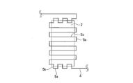
- FIG. 3 is a cross-sectional view taken along line III-III in FIG.
- FIG. 3 shows the structure of the detection circuit which detects the change of the resistance value of wiring.
- FIG. 7 is a cross-sectional view taken along line IX-IX of FIG. It is a top view by the side of a light extraction surface showing composition of an optical member concerning a 3rd embodiment. It is a bottom view of the holding member of FIG. It is a top view of the heat radiating member of FIG.
- FIG. 11 is a cross-sectional view taken along line XIII-XIII of FIG. It is sectional drawing which shows the modification of the optical member which concerns on 1st Embodiment.
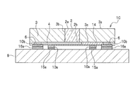
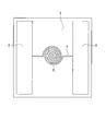
- the optical member 1A includes the conversion member 2, the holding member 3 and the wiring 4. Further, it is preferable that the optical member 1A includes the heat dissipation member 9.
- the light emitting device 20 preferably includes the optical member 1A and the laser element 25 and the package 21. More preferably, the light emitting device 20 includes the detection circuit 30.
- each component of the optical member 1A and the light emitting device 20 will be described.
- the conversion member 2 is a member having a first surface to be the light extraction surface 2 a and capable of converting laser light which is excitation light emitted from the laser element 25 into light of different wavelengths.
- the conversion member 2 has a surface opposite to the light extraction surface 2a (first surface) as a light irradiation surface 2b on which the laser beam from the laser element 25 is incident. Since the wiring 4 is formed on the light extraction surface 2a (first surface) which is the surface side of the conversion member 2, connection to an external power source or circuit for energizing the wiring 4 is facilitated.
- the conversion member 2 is preferably made of an inorganic material so as to be difficult to be decomposed by the irradiation of the laser beam.
- the conversion member 2 made of an inorganic material include ceramics or glass containing a phosphor capable of wavelength conversion of laser light, and a single crystal of a phosphor.
- the conversion member 2 is preferably a material having a high melting point, and the melting point is preferably 1300 to 2500 ° C. Since the conversion member 2 is formed of such a material having good light resistance and heat resistance, it is difficult to cause deterioration even when irradiated with high density light such as laser light, and is held by the holding member 3 Deformation and discoloration are less likely to occur due to heat during the process. Therefore, it is preferable that the conversion member 2 be formed of a material having good light resistance and heat resistance.
- cerium-activated yttrium aluminum garnet (YAG), cerium-activated lutetium aluminum garnet (LAG), europium and / or chromium-activated nitrogen-containing Examples include calcium aluminosilicate (CaO-Al 2 O 3 -SiO 2 ), europium-activated silicate ((Sr, Ba) 2 SiO 4 ), ⁇ -sialon phosphor, ⁇ -sialon phosphor, and the like.
- YAG which is a fluorescent substance having good heat resistance.
- a material obtained by sintering a phosphor and a translucent material such as aluminum oxide (Al 2 O 3 , melting point: about 1900 ° C. to 2100 ° C.) may be mentioned.
- the content of the phosphor is preferably 0.05 to 50% by volume, more preferably 1 to 30% by volume, with respect to the total volume of the ceramic.
- a ceramic substantially consisting of only a phosphor, which is formed by sintering a powder of a phosphor without using such a translucent material may be used as the conversion member 2.
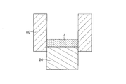
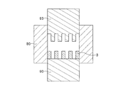
- the holding member 3 is a member which holds the conversion member 2 and has a surface 3 a (second surface) continuous on the same plane as the light extraction surface 2 a (first surface) of the conversion member 2.
- the holding member 3 has a through hole 3b penetrating in the thickness direction, and is connected to the conversion member 2 in a state where the conversion member 2 is inserted into the through hole 3b, thereby holding the conversion member 2 .
- the shape of the through hole 3 b is preferably made to correspond to the shape of the conversion member 2, and may be, for example, a pillar shape, a cone shape, a truncated cone, a truncated pyramid or a combination thereof. Besides polygons such as quadrilaterals, they may be circular or oval.
- the thickness of the holding member 3 is preferably 0.2 mm or more in consideration of the strength. Further, the thickness of the holding member 3 may be any thickness that can hold the conversion member 2 and is preferably 2.0 mm or less in order to suppress cost increase and increase in the height of the optical member 1A.
- the holding member 3 is a material that reflects the laser light and the fluorescence emitted by the phosphor with high reflectance, and is made of a material with high thermal conductivity that exhausts the heat of the conversion member 2 held in the through hole 3b.
- Materials having high reflectance and high thermal conductivity include light reflective ceramics, metals, or composites of ceramics and metals. It is preferable that it is light-reflective ceramics in which a high reflectance is easy to be obtained. It is preferable to use alumina (Al 2 O 3 ) ceramic as the light reflective ceramic.
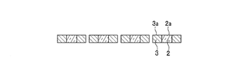
- the wiring 4 is a linear body continuously formed from the light extraction surface 2 a (first surface) of the conversion member 2 to the surface 3 a (second surface) of the holding member 3.
- the wiring 4 is not limited to being formed directly on the surfaces of the conversion member 2 and the holding member 3, and may be formed via a film such as a light transmitting film 7 (see FIG. 14). Further, in plan view, the wiring 4 has a shape of one stroke.
- the wiring 4 is electrically connected to the conduction unit 6 for conduction at both ends thereof.
- the wiring 4 crosses the boundary between the conversion member 2 and the holding member 3 from the light extraction surface 2 a (first surface) of the conversion member 2 to the surface 3 a (second surface) of the holding member 3. Are formed continuously.
- the breakage of the wiring 4 is not limited to the disconnection of the wiring 4 but also includes partial or entire thinning or thinning due to chipping or the like.
- the resistance value of the wiring 4 is changed due to thinning or the like, and the voltage value is changed, so that the difference from the normal state can be known, and member damage can be detected.
- damage to the conversion member 2 and the holding member 3 in the vicinity of the boundary can be detected, it is possible to more accurately detect an abnormality that leads to a laser beam leak.
- the boundary between the members can be arranged at a position where the laser light easily hits. Can be reduced to achieve high brightness.
- the wiring 4 covers at least a part of the light extraction surface 2a (first surface) of the conversion member 2 and has a shape in which a part has a plurality of bending parts 5a in a plan view, and at least one of the plurality of bending parts 5a. Preferably, one is formed over the surface 3 a (second surface) of the holding member 3.
- the number and the pitch of the bent portions 5a in the bellows shape as shown in FIG. 2 are appropriately set in consideration of the size of the through holes 3b of the holding member 3 and the width of the wiring 4.
- the wiring 4 When the wiring 4 has a bellows shape, a plurality of locations where the wiring 4 straddles the boundary between the conversion member 2 and the holding member 3 will be set, and damage to the conversion member 2 and the holding member 3 in the vicinity of the boundary will be detected. Accuracy is improved. In other words, it can be said that the wiring 4 shown in FIGS. 1 to 3 has a shape having an extending portion 5b extending in one direction and a bending portion 5a connecting the adjacent extending portions 5b.
- the wiring 4 is made of a conductive material generally used as a wiring of the light emitting device 20.
- the wiring 4 is preferably made of a translucent conductive material in order to suppress a decrease in luminance of light extracted from the conversion member 2.
- ITO indium tin oxide
- the conducting portion 6 electrically connected at both ends of the wiring 4 can also be formed in a film shape using a conductive material.
- a metal layer such as a Ti / Pt / Au layer is provided on the ITO layer to improve the adhesion of the wire etc. It is preferable to do.
- the wiring 4 preferably has a thickness of 50 to 200 nm at least above the conversion member 2 in order to suppress uneven brightness of light extracted from the conversion member 2.
- the width of the wiring 4 is preferably 5 to 50 ⁇ m. If the thickness of the wiring 4 is less than 50 nm or the width is less than 5 ⁇ m, breakage such as disconnection easily occurs in the wiring 4 even if the conversion member 2 and the holding member 3 are not damaged, leading to erroneous detection of member breakage easy. In addition, when the thickness of the wiring 4 exceeds 200 nm or the width exceeds 50 ⁇ m, it becomes difficult to suppress the luminance unevenness of the light extracted from the conversion member 2.
- the heat radiating member 9 is a translucent member disposed on the back surface 3 c side of the holding member 3 and transmitting the laser beam from the laser element 25. It is preferable to use sapphire which is a light transmitting material having a high thermal conductivity as a main member constituting the heat dissipation member 9. By providing the heat dissipation member 9, the heat from the conversion member 2 can be efficiently dissipated.
- the thickness of the heat dissipation member 9 is, for example, 0.2 to 1 mm, preferably 0.4 to 0.6 mm.
- the first metal layer 10 and the second metal layer 11 can be used to join the heat dissipation member 9 and the holding member 3.
- the first metal layer 10 and the second metal layer 11 are made of a metal material containing at least one selected from gold, tin, silver, nickel, rhodium, aluminum, tungsten, platinum, titanium, ruthenium, molybdenum, niobium Is preferred.
- the first metal layer 10 and the second metal layer 11 are, for example, a laminated film made of a titanium film, a platinum film and a gold film, or a laminated film made of a mixed film made of a titanium film, a platinum film, a gold film and a gold-tin alloy. It is a membrane.
- the first metal layer 10 is formed on the holding member 3 side, and the second metal layer 11 is formed on the heat dissipation member 9 side.
- a gold-tin alloy is formed on either one of the first metal layer 10 and the second metal layer 11, the first metal layer 10 and the second metal layer 11 are brought into contact, and heating is performed to a temperature above the melting point of the gold-tin alloy. By doing this, the heat dissipating member 9 and the holding member 3 can be joined.
- the thickness of each of the first metal layer 10 and the second metal layer 11 can be, for example, 0.1 to 5 ⁇ m.
- the first metal layer 10 is made Ti (6 nm) / Pt (200 nm) / Au (300 nm) in order from the holding member 3 side
- the second metal layer 11 is in order from the heat dissipation member 9 side (6 nm) / Pt (200 nm) / Au (50 nm) / AuSn (3 ⁇ m) can be mentioned.
- joining members such as the first metal layer 10 and the second metal layer 11 are not formed at positions facing the conversion member 2.
- the laser beam is not blocked by the bonding member such as the first metal layer 10 or the like.
- the first metal layer 10 is formed to surround the light irradiation surface 2 b of the conversion member 2 facing the heat dissipation member 9. Therefore, the first metal layer 10 and the heat dissipation member 9 can effectively prevent the adhesion of dust to the light irradiation surface 2 b of the conversion member 2.
- the laser element 25 is arranged to irradiate the conversion member 2 with a laser beam.
- the laser element 25 has higher energy as the emitted laser beam has a shorter wavelength, and detection of a leak of the laser beam is more required. Therefore, it is preferable to use an element that emits a short wavelength laser beam as the laser element 25 .
- a laser element a semiconductor laser element made of a nitride semiconductor can be mentioned.
- the laser element 25 can be provided with a configuration for irradiating the conversion member 2 with the laser light, for example, the reflection member 26 in the optical path.
- the reflection member 26 a member in which a reflection film is provided on the slope of the main body made of glass or the like having a shape such as a triangular prism or a quadrangular pyramid can be used.
- the angle of the slope with respect to the bottom of the main body is preferably about 45 degrees in order to guide the laser light in the orthogonal direction.
- the package 21 encloses the laser element 25.
- the package 21 is a storage body having a storage portion such as the concave portion 27 and the like, in which the laser element 25 and the reflection member 26 are disposed and stored.
- the package 21 mainly includes a housing main body 22 made of a ceramic such as aluminum oxide, aluminum nitride, silicon nitride, silicon carbide or a metal such as Cu, and a lid 24 joined to the housing main body 22 by welding or the like.
- the storage body portion 22 can have a recess 27 opened on the upper surface side. At the periphery of the recess opening, a frame-shaped welding portion 23 containing iron as a main component for welding with the lid portion 24 may be provided.
- the storage body portion 22 is formed such that at least one surface of the upper surface continuous with the opening of the recess 27 is wider than the other surfaces, and the electrode portion 28 is disposed.
- the electrode part 28 may arrange
- a lead terminal is used as the electrode 28.
- the lid portion 24 hermetically seals the laser element 25 by being joined to the housing main portion 22 by welding or the like. Thereby, adhesion of dust such as organic matter to the laser element 25 can be suppressed.
- the lid portion 24 may have a support portion 24 a welded to the storage body portion 22, a light transmitting portion 24 b for transmitting a laser beam, and a bonding material 24 c for bonding the support portion 24 a and the light transmitting portion 24 b. it can.
- a material containing iron as a main component can be used for the support portion 24a. Glass, sapphire, etc. can be used for the light transmission part 24b. Low melting point glass, gold-tin solder or the like can be used as the bonding material 24c.
- the laser beam emitted from the laser element 25 is reflected by the reflection member 26, passes through the light transmitting portion 24 b and the heat dissipation member 9, and is irradiated to the light irradiation surface 2 b of the conversion member 2.
- the package 21 includes an electrode portion 28 exposed on the top surface of the storage body portion 22.
- the entire surface of the lower surface of the package 21 may be mounted on another member such as a heat sink by providing the electrode portion 28 electrically connected to the outside on the surface other than the lower surface of the storage main body 22. it can. Therefore, the package 21 easily dissipates the heat generated by the light emitting device 20 to the heat sink.
- the detection circuit 30 is a circuit that detects a change in resistance value caused by the breakage of the wiring 4.
- the light emitting device 20 is a circuit connected to the conductive circuit of the wiring 4 and the laser element 25.
- breakage of the conversion member 2 and the holding member 3 can be detected by a change in resistance value caused by breakage of the wiring 4. Then, when a change in the resistance value of the wiring 4 is detected, it is determined that the conversion member 2 and the holding member 3 are damaged, and the driving of the laser element 25 is stopped to prevent the leakage of the laser light. Can.
- the detection circuit 30 only needs to be able to detect the breakage of the wiring 4.
- the detection circuit 30 has a circuit configuration shown in FIG. As shown in FIG. 4, the detection circuit 30 detects a change in resistance value due to the breakage of the wiring 4 based on a change in voltage value.
- the detection circuit 30 includes a first connection conductor 31 and a second connection conductor 32.
- a power supply for conduction is connected to the first connection conducting wire 31, and the wiring 4, the laser element 25 and the switch element 33 are connected.
- a voltage detection resistor 34 is connected to the second connection wire 32.
- the wire 4 and the voltage detection resistor 34 are energized by the energizing power supply.
- the switch element 33 controls the driving stop of the laser element 25 by comparing the voltage of the voltage detection resistor 34 with the reference voltage.
- the resistance value of the wiring 4 is normally low and the voltage of the wiring 4 is low. Therefore, the voltage of the voltage detection resistor 34 is relatively high. It becomes above.
- the drive of the laser element 25 is continued according to the input from the switch element 33.
- the resistance of the wiring 4 is increased due to the breakage of the wiring 4, the voltage of the wiring 4 is increased, and the voltage of the voltage detection resistor 34 is relatively decreased.
- the drive of the laser element 25 is stopped.
- the switch element 33 an operational amplifier, a comparator, a bipolar transistor, a MOSFET (metal-oxide-semiconductor field-effect transistor) or the like can be used.
- a transistor element such as a MOSFET whose on / off can be controlled by the voltage of the voltage detection resistor 34 is preferable.
- the switch element 33 is, for example, a transistor element such as a MOSFET, and may be one that is turned on when the voltage of the voltage detection resistor 34 is equal to or higher than the reference voltage. As a result, when the voltage of the voltage detection resistor 34 decreases and becomes less than the reference voltage, the switch element 33 is turned off, and the current supply to the laser element 25 can be automatically stopped.
- the optical member 1A is fixed to the package 21 so that the laser light that has passed through the light transmitting portion 24b and the heat dissipation member 9 from the recess 27 reaches the conversion member 2. Then, it is preferable that the plurality of bent portions 5 a of the wiring 4 be arranged to straddle the boundary between the conversion member 2 and the holding member 3. With such an arrangement, breakage of the boundary between the conversion member 2 and the holding member 3 can be detected accurately by the wiring 4.
- the heat dissipating member 9 and the first metal layer 10 can be used to fix the optical member 1A to the package 21.
- the method of manufacturing an optical member includes (1) preparing a sintered body, and (2) removing a part of the conversion member and the holding member, And (3) including the step of forming a wiring. Each step will be described below.
- Step of Preparing a Sintered Body As shown in FIG. 5A, in the step of preparing a sintered body, the converting member 2 and the holding member 3 are brought into contact with each other to prepare an integrally formed sintered body 100. It is a process.
- the method of obtaining the sintered body 100 includes, for example, a step of preparing the conversion member 2, a step of forming a molded body to be the holding member 3, and a step of sintering the conversion member 2 and the molded body. The method is mentioned.
- a sintered body refers to a material obtained by heating a powdery material at a temperature lower than its melting point and hardening it.
- the conversion member 2 formed of a molded article and the holding member 3 of powder particles not yet sintered are heat-treated as in the present manufacturing method, the conversion member 2 formed of a molded article It is considered that a sintering phenomenon similar to a general sintering phenomenon has occurred on the surface and the surface of the holding member 3 of powder particles. Therefore, in this specification, what integrally formed the conversion member 2 which consists of molded articles, and the holding member 3 of powder particles is also called a sintered compact. Similarly, a member in which the powder particle conversion member 2 and the holding member 3 made of a molded product are integrally formed is also referred to as a sintered body.
- a sintering method for example, a discharge plasma sintering method (SPS method: spark plasma sintering method) or a hot press sintering method (HP method: hot pressing method) can be used.
- SPS method spark plasma sintering method
- HP method hot press sintering method
- the sintering temperature is preferably set to 1200 ° C. or more and 1800 ° C. or less, and more preferably set to 1400 ° C. or more and 1500 ° C. or less.
- the temperature is preferably set to 1200 ° C. or higher, the strength of the holding member 3 can be secured. Further, by setting the temperature to 1800 ° C. or less, the possibility that the light transmitting property of the holding member 3 becomes high can be reduced.
- the plurality of sintered bodies 100 are singulated so that one sintered body 100 includes one conversion member 2.
- a plurality of sintered bodies 100 can be singulated by using one or more of scribing, dicing, and breaking.
- one sintered body 100 is singulated so as to include one conversion member 2
- one sintered body 100 is singulated so as to include a plurality of conversion members 2. It is also good.
- Step of Forming Wiring This is a step of forming the wiring 4 continuously from the light extraction surface 2 a (first surface) of the conversion member 2 to the surface 3 a (second surface) of the holding member 3.
- Examples of the method for forming the wiring 4 include sputtering, chemical vapor deposition, and atomic layer deposition.
- the wiring 4 is continuously formed from the light extraction surface 2 a (first surface) of the conversion member 2 to the surface 3 a (second surface) of the holding member 3, the light extraction surface 2 a (first The breakage in the vicinity of the boundary between the surface) and the surface 3 a (second surface) of the holding member 3 can be detected by the breakage of the wiring 4. As a result, it is possible to detect an abnormality that leads to a laser beam leak more accurately.
- the method of manufacturing the optical member 1A includes, after the step of forming the wiring, a bonding step of bonding the heat dissipation member 9 and the holding member 3 using the first metal layer 10 formed by the sputtering method or the like.
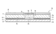
- the optical member 1 B used for the light emitting device 20 includes the conversion member 2, the holding member 3, and the wiring 4. Moreover, it is preferable that the optical member 1B includes the heat dissipation member 9.
- the light emitting device 20 preferably includes the optical member 1 B and the laser element 25 and the package 21. As in the light emitting device 20 according to the first embodiment, the light emitting device 20 more preferably includes the detection circuit 30. The components of the optical member 1B and the light emitting device 20 will be described. The same as the optical member 1A and the light emitting device 20 shown in FIGS. 1 to 4 except for the matters described below.
- the light irradiation surface 2b on the back surface side of the conversion member 2 that is the heat dissipation member 9 side is the first surface.
- the wiring 4 is continuously formed across the boundary from the light irradiation surface 2 b (first surface) to the back surface 3 c (second surface) of the holding member 3. That is, the wiring 4 is disposed between the conversion member 2 and the holding member 3 and the heat dissipation member 9.
- the conversion member 2 has a surface opposite to the light irradiation surface 2b as a light extraction surface 2a from which the wavelength-converted light is emitted.
- the wavelength-converted light extracted from the conversion member 2 is not affected by the wiring 4, thereby reducing the uneven brightness. be able to.
- the 2nd metal layer 11 is used for joining of the holding member 3 and the thermal radiation member 9 in the optical member 1B.
- the first metal layer 10 includes the center-side first metal layer 10 a and the end-side first metal layer 10 b, and has a role of bonding the holding member 3 and the heat dissipation member 9.
- the constituent material and thickness of the center side first metal layer 10 a and the end side first metal layer 10 b are the same as those of the first metal layer 10 of the optical member 1 A.
- the center-side first metal layer 10a is a center of the back surface 3c (second surface) of the holding member 3 so as to surround the wiring 4 formed on the light irradiation surface 2b (first surface) surface of the conversion member 2 in plan view. Is formed in a rectangular ring shape.
- the central side first metal layer 10 a is electrically connected to the wiring 4, detection of breakage of the wiring 4 becomes difficult. Therefore, the central side first metal layer 10 a is insulated from the wiring 4 by being disposed through the wiring 4 and the insulating film 14. As the area where the central first metal layer 10a and the wiring 4 overlap in a plan view has a smaller area, the possibility of leakage between the central first metal layer 10a and the wiring 4 can be reduced. For this reason, as shown in FIG. 7, it is preferable to place the central first metal layer 10a and the wiring 4 in only two places in plan view. In order to achieve such an arrangement, the central side first metal layer 10 a may be arranged outside the bent portion 5 a of the wiring 4.
- the end-side first metal layer 10b is formed in a rectangular shape on the left and right, respectively, separated from the center of the back surface 3c on which the center-side first metal layer 10a is formed so as to cover the two conducting parts 6 for energizing the wiring 4. It is done.
- the two end-side first metal layers 10 b are electrically connected to the wiring 4, respectively, and serve as the anode and the cathode of the wiring 4.
- the second metal layer 11 includes a center-side second metal layer 11 a and an end-side second metal layer 11 b.
- the constituent material and thickness of the center side second metal layer 11a and the end side second metal layer 11b are the same as those of the second metal layer 11 of the optical member 1A.
- the central second metal layer 11a is formed on the central side of the surface of the heat dissipation member 9 facing the holding member 3 so as to cover the central first metal layer 10a formed on the back surface 3c (second surface). There is.
- the center-side second metal layer 11 a is formed in a rectangular ring shape so as to surround the wiring 4 in the same manner as the center-side first metal layer 10 a.
- the end-portion-side second metal layer 11 b is formed in a rectangular shape on the left and right of the surface of the heat dissipation member 9 facing the holding member 3 while being separated from the center-side second metal layer 11 a.
- the end-portion-side second metal layer 11 b is formed in a rectangular shape having a size such that a part thereof protrudes outward from the holding member 3 in plan view when the holding member 3 and the heat dissipation member 9 are joined.
- the two end-side second metal layers 11 b are electrically connected to the current-carrying portions 6 (end-side first metal layers 10 b), respectively, in addition to the bonding of the holding member 3 and the heat dissipation member 9. It has a role of supplying electricity from the outside to the conduction part 6 of the above.
- the end-portion-side second metal layer 11 b is arranged so that a portion thereof is exposed from the holding member 3 in plan view after bonding. Thereby, a wire etc. can be connected to the part exposed from the holding member 3.
- the end-side second metal layer 11b can be easily pulled out by disposing the end-side second metal layer 11b connected to the outside outside the center-side second metal layer 11a.
- the center-side first metal layer 10 a and the center-side second metal layer 11 a are formed together with the heat dissipation member 9 so as to surround the light irradiation surface 2 b (first surface) of the conversion member 2. Therefore, it is possible to effectively prevent the adhesion of dust to the light irradiation surface 2 b (first surface) of the conversion member 2.
- the planar view shape of the center side 1st metal layer 10a and the center side 2nd metal layer 11a is cyclic
- the insulating film 14 is a film that insulates the central side first metal layer 10 a and the wiring 4.
- the insulating film 14 is disposed at least in a portion where the central first metal layer 10 a and the wiring 4 overlap in a plan view. In the case where the insulating film 14 is also disposed on the path of the laser light, the insulating film 14 is preferably translucent.
- the insulating film 14 is a light irradiation surface 2b (first surface) of the conversion member 2 excluding the region where the two conducting parts 6 for energizing the wiring 4 are formed, the back surface 3c (second surface) of the wiring 4 and the holding member 3 Can be formed to cover the whole of.
- the insulating film 14 may double as the protective film 8 in the modification of the first embodiment described later.
- the constituent material and thickness can be the same as that of the protective film 8.
- the light emitting device 20 is different from the light emitting device 20 in that the optical member 1B is used instead of the optical member 1A. It is the same as that of one embodiment.
- the light emitting device 20 having such a configuration can reduce the luminance unevenness of the extracted light by using the optical member 1B.
- the optical member 1B can be manufactured by the same manufacturing method as that of the first embodiment.
- the optical member 1B manufactures the light irradiation surface 2b of the conversion member 2 as a 1st surface in which the wiring 4 is formed.
- the central first metal layer 10a and the end first metal layer 10b formed by sputtering or the like, and the central second metal layer 11a are included.
- an optical member 1C according to the third embodiment has a part of the optical member 1B according to the second embodiment modified. That is, in the optical member 1C, the second metal layer on the center side of the second metal layer 11 is changed in shape so that a part thereof is exposed from the holding member 3 in a plan view, and becomes the leak checking electrode 15.
- the optical member 1 ⁇ / b> C includes the conversion member 2, the holding member 3, the wiring 4, the first metal layer 10, the insulating film 14, the leak check electrode 15, the wiring electrode 16, and the heat dissipation member 9.
- the light emitting device 20 preferably includes the optical member 1C and the laser element 25 and the package 21. More preferably, the light emitting device 20 includes the detection circuit 30. Each component of the optical member 1C will be described. The same as the optical member 1B shown in FIGS. 6 to 9 except for the matters described below.
- the leak check electrode 15 includes a central portion 15a and a terminal portion 15b connected to the central portion 15a via a linear connection portion 15c.
- the leak checking electrode 15 is used to check whether insulation between the central first metal layer 10 a and the wiring 4 can be secured after the holding member 3 and the heat radiating member 9 are joined.
- the leak check electrode 15 is electrically connected to the central first metal layer 10a.
- the terminal portion 15b of the leak check electrode 15 is used as an anode, a voltage is applied between the leak check electrode 15 and the cathode side of the wiring electrode 16, and it is checked whether current flows or not. And it can be determined whether the wiring 4 is leaking.
- the anode and the cathode may be reversed.
- the central portion 15a is formed in a rectangular ring shape on the heat dissipation member 9 side so as to cover the central first metal layer 10a formed so as to surround the conversion member 2 (first surface) in plan view.
- the central portion 15a can be formed to have the same size as the central first metal layer 10a.
- the terminal portion 15b is electrically connected to the outside, when the holding member 3 and the heat dissipation member 9 are joined, the terminal portion 15b is formed in such a size and position that a part thereof protrudes outward from the holding member 3 in plan view. ing.
- the terminal portion 15b is electrically connected to the central portion 15a via the connection portion 15c.
- the terminal portion 15 b is formed on the heat dissipation member 9 side in a rectangular shape along one side of the heat dissipation member 9.
- the central portion 15a, the connection portion 15c, and the terminal portion 15b correspond to the central second metal layer 11a in the optical member 1B, and the constituent material and thickness are the same as those of the central second metal layer 11a in the optical member 1B. It can be done.
- the central portion 15 a, the connection portion 15 c, and the terminal portion 15 b are also used to join the holding member 3 and the heat dissipation member 9.
- the wiring electrode 16 corresponds to the end-side second metal layer 11b in the optical member 1B, and the shape is different only from the end-side second metal layer 11b, and the constituent material and the thickness are the same. be able to.
- the wiring electrode 16 includes a central portion 16a and a terminal portion 16b connected to the central portion 16a via a linear connection portion 16c.
- the central portion 16a has the same size as the end-side first metal layer 10b in order to electrically connect to the two current-carrying portions 6 via the end-side first metal layer 10b to energize the wiring 4.
- the heat dissipation member 9 is formed in a rectangular shape on the side.
- the terminal portion 16b When joining the holding member 3 and the heat radiation member 9, the terminal portion 16b has a rectangular shape at a corner portion of the heat radiation member 9 so as to have a size and a position in which a part protrudes outward from the holding member 3 in plan view. It is formed.
- the central portion 16a and the terminal portion 16b are formed to be electrically connected via the connection portion 16c.
- the central portion 16 a, the connection portion 16 c, and the terminal portion 16 b are also used to join the holding member 3 and the heat dissipation member 9.
- the light emitting device 20 is the same as the second embodiment except that an optical member 1C is used instead of the optical member 1B in the light emitting device 20 (see FIG. 9) using the optical member 1B of the second embodiment.
- the insulating film 14 is a film similar to the protective film 8 (see FIG. 14).
- the leak check electrode 15 central portion 15a and terminal portion 15b is a bonding layer similar to the central second metal layer 11a and the end second metal layer 11b (see FIGS. 8 and 9).
- the optical member 1C can be manufactured by the same manufacturing method as that of the second embodiment.
- the electrode 15 for checking leakage center portion A bonding step may be included in which the heat dissipation member 9 and the holding member 3 are bonded by using the connection portion 15c and the terminal portion 15b) and the wiring electrode 16 (the central portion 16a, the connection portion 16c and the terminal portion 16b).
- an optical member 1 D which is a modification of the optical member 1 A according to the first embodiment, includes the conversion member 2, the holding member 3, the wiring 4, the translucent film 7, and the protective film 8. And a heat dissipation member 9, a dielectric multilayer film 17, and an antireflective film 18.
- the optical member 1D may include one or more of the translucent film 7, the protective film 8, the dielectric multilayer film 17, and the antireflection film 18.
- the conversion member 2, the holding member 3, the wiring 4, and the heat dissipation member 9 of the optical member 1D are the same as those of the optical member 1A, and thus the description thereof is omitted.
- the translucent film 7, the protective film 8, the dielectric multilayer film 17 and the antireflective film 18 of the optical member 1D will be described below.
- the translucent film 7 is a film that covers the light extraction surface 2 a (first surface) of the conversion member 2 and the surface 3 a (second surface) of the holding member 3.
- the flatness of the surfaces of the conversion member 2 and the holding member 3 can be improved.
- the wiring 4 is not directly formed on the surfaces of the conversion member 2 and the holding member 3 but is formed on the surface of the light transmitting film 7. Therefore, since the wiring 4 is formed on the surface of the light transmitting film 7 in which the flatness of the surface is improved more than the conversion member 2 and the holding member 3, the possibility of disconnection of the wiring 4 at the time of formation is reduced. it can.
- the conversion member 2 is made of two or more kinds of materials, if the surface of the conversion member 2 is subjected to a planarization process such as CMP, the removal rate is different depending on the material, and thus a level difference easily occurs on the surface. For this reason, it is preferable to form the translucent film 7 on the surface of the conversion member 2. Similarly, even when the holding member 3 is formed of light-reflecting ceramic, the ceramic tends to have a higher porosity as it is highly reflective, and the flatness of the surface of the holding member 3 is poor. Preferably, the light transmitting film 7 is formed.
- the translucent film 7 is made of a translucent material.
- a translucent material which is translucent to visible light a material containing silicon oxide such as SiO 2 may be mentioned.
- the translucent film 7 is, for example, a SiO 2 film.
- the thickness of the light transmitting film 7 is preferably such that the flatness of the conversion member 2 and the holding member 3 can be improved, and specifically, it is preferably 1 to 15 ⁇ m.
- the light transmitting film 7 may be formed to cover the light irradiation surface 2 b of the conversion member 2 and the back surface 3 c of the holding member 3.
- the protective film 8 is a translucent film formed so as to cover at least the light extraction surface 2 a (first surface) of the conversion member 2 and the wiring 4.
- the protective film 8 is formed to cover the entire light extraction surface 2a (first surface).
- the wiring 4 can be protected so that the wiring 4 is not damaged by a slight impact that does not damage the conversion member 2.
- the thickness of the protective film 8 is, for example, not less than the wavelength of excitation light (for example, 450 nm) and not more than 20 ⁇ m.
- the protective film 8 is made of a translucent material in the same manner as the translucent film 7.
- a translucent material which is translucent to visible light a material containing silicon oxide such as SiO 2 may be mentioned.
- the protective film 8 is, for example, a SiO 2 film.
- the refractive index of the protective film 8 be a value close to the refractive index of the wiring 4 and the protective film 8 be disposed at least in a region where the wiring 4 is not formed. Thereby, the difference in refractive index between the region in which the wiring 4 is formed and the region in which the wiring 4 is not formed can be reduced, and unevenness in luminance can be reduced.
- the protective film 8 preferably contains silicon oxide and a material having a refractive index higher than silicon oxide. As described above, when the protective film 8 contains a material having a high refractive index, the uneven brightness can be improved as described above. Specifically, for the protective film 8, it is preferable to use a material in which a predetermined amount of tantalum oxide is mixed with silicon oxide.
- the protective film 8 can be, for example, a film in which SiO 2 and Ta 2 O 5 are mixed. If the wiring 4 is ITO, the protective film 8, SiO 2 is suitable to be a mixed film of SiO 2 and Ta 2 O 5 of about 25 to 35 wt%.
- the dielectric multi-layered film 17 is a multi-layered film disposed on the top surface of the heat dissipating member 9 on the side of the conversion member 2 and the holding member 3.
- the dielectric multilayer film 17 is formed by laminating, for example, two or more dielectric films having different refractive indexes, which are made of a dielectric such as aluminum nitride, silicon oxide, aluminum oxide, zirconium oxide, titanium oxide, niobium oxide or tantalum oxide. It is
- the dielectric multilayer film 17 is a film that transmits the laser light from the laser element 25 and reflects wavelength conversion light from the light irradiation surface 2 b of the conversion member 2.
- the dielectric multilayer film 17 is a film that has a higher reflectance to the light wavelength-converted by the conversion member 2 than to the excitation light (laser light from the laser element 25). As a result, the light traveling from the conversion member 2 toward the laser element 25 can be reflected back to the conversion member 2, so that the light extraction efficiency from the light extraction surface 2 a of the conversion member 2 can be improved.
- the thickness of the dielectric multilayer film 17 can be, for example, 1 to 10 ⁇ m.
- the anti-reflection film 18 is a film disposed on the lower surface which is the surface of the heat radiation member 9 on which the laser light is incident.
- the antireflective film 18 is made of, for example, a dielectric material mainly composed of at least one selected from aluminum nitride, silicon oxide, aluminum oxide, zirconium oxide, titanium oxide, niobium oxide, and tantalum oxide.
- the antireflective film 18 is a film having a very small value, such as 1% or less, of the reflectance to the laser light from the laser element 25 by adjusting the thickness, the composition ratio, and the like. By providing the anti-reflection film 18, it is possible to increase the amount of incident laser light to the conversion member 2.
- the thickness of the antireflective film 18 can be, for example, 0.2 to 1 ⁇ m.
- an optical member 1E which is a modification of the optical member 1B according to the second embodiment, includes the conversion member 2, the holding member 3, the wiring 4, the translucent film 7, and the heat dissipation member 9. And a dielectric multilayer film 17 and an antireflective film 18.
- an optical member 1F which is a modification of the optical member 1C according to the third embodiment, includes the conversion member 2, the holding member 3, the wiring 4, the light transmitting film 7 and the heat dissipation member 9, the dielectric multilayer film 17, and the antireflective film 18.
- the light transmitting film 7, the protective film 8, the dielectric multilayer film 17, and the antireflection film 18 can be provided.
- the conversion member 2, the holding member 3, the wiring 4, and the heat dissipation member 9 of the optical members 1E and 1F are the same as those of the optical member 1B.
- the translucent film 7, the dielectric multilayer film 17, and the anti-reflection film 18 of the optical members 1E and 1F are the same as those of the optical member 1D.
- the translucent films 7 of the optical members 1E and 1F are formed to cover the light irradiation surface 2b (first surface) of the conversion member 2 and the back surface 3c (second surface) of the holding member 3.
- the translucent film 7 covering the surface on which the wiring 4 is provided (that is, the light irradiation surface 2 b and the back surface 3 c), as described above, the possibility of the wiring 4 breaking during formation is reduced.
- the light transmitting film 7 may be formed to cover the light extraction surface 2 a of the conversion member 2 and the surface 3 a of the holding member 3.
- FIG. 17A Showe of wiring
- a part of the spiral-shaped portion of the wiring 4 covers the conversion member 2, and another part is formed on the holding member 3.
- the number of turns and the pitch in the spiral shape are appropriately set in consideration of the size of the through hole 3 b of the holding member 3 and the width of the wiring 4.
- the wiring 4 has a bellows shape as shown in FIG. 2, for example, if a crack extending in the lateral direction in the drawing is generated in the conversion member 2, the conversion member 2 is broken but the wiring 4 is not broken. obtain.
- the wiring 4 is broken and it is possible to detect an abnormality, regardless of whether it is a crack in the horizontal direction or a crack in the vertical direction in the drawing.
- the pitch of the spiral shape be 60 ⁇ m or less.
- the pitch of the spiral shape is, in other words, the width of the passage portion which is a portion where the wiring 4 is not provided.
- the pitch of the spiral shape is preferably 5 ⁇ m or more so that the passage portion is not crushed when the wiring 4 is formed.
- the wiring 4 shown by each embodiment and modification is a shape which the extending
- the allowance of the shift in the width direction of the stretched portion 5b is equal to or less than the width of the outermost stretched portion 5b, and when shifted more than that, the outermost stretched portion 5b is the conversion member 2 And does not overlap with the boundary between
- FIG. 17B the wiring 4 shown by each embodiment and modification is a shape which the extending
- the misalignment is permitted.
- the capacitance can be made larger than the width of the wiring 4.
- the respective extending portions 5b are connected by the bending portion 5a, whereby the wiring 4 has a single-stroke writing shape.
- the wiring 4 shown in each of the embodiments and the modifications intersects with any of the sides forming the outer edge of the conversion member 2. It may be a one-stroke writing shape having a plurality of stretched portions 5b to be stretched and a bent portion 5a connecting the adjacent stretched portions 5b.
- the extension direction of the portion other than the bending portion 5a in the wiring 4 overlapping the conversion member 2 is only one direction, the allowable amount of deviation of the wiring 4 with respect to the boundary between the conversion member 2 and the holding member 3 is shown in FIGS. It can be expanded more than the case of the wiring 4 shown.
- the bending part 5a is formed in linear form, curvilinear forms, such as semicircle, may be sufficient.
- the stretched portion 5b is also formed in a linear shape, it may have a shape other than the linear shape, such as repeating the unevenness of the straight line or repeating the unevenness of the curve.
- the modified example of the method of manufacturing the optical member 1A of the first embodiment includes (1) preparing a sintered body, (2) removing a part of the conversion member and the holding member, and (A) heat treating And (B) forming a light-transmissive film, and (3) forming a wiring.
- the steps (1) to (3) are the same as the above-described manufacturing method, and thus the description thereof is omitted.
- the steps (A) and (B) will be described below.
- the same modification can be adopted in the method of manufacturing the optical members 1B and 1C according to the second and third embodiments.
- the residual organic matter is produced by heating the holding member 3 in a state where at least a part of the route through which the organic matter escapes is blocked by the wiring 4 or the like in a later step. It becomes black and causes the appearance abnormality of the holding member 3 to occur. Therefore, by performing the heat treatment before forming the wiring 4 and the like, the residual organic substance in the holding member 3 can be reduced, and the possibility of the appearance abnormality of the holding member 3 can be reduced.
- the temperature of the heat treatment is preferably lower than the sintering temperature of the sintered body constituting the holding member 3. This can reduce the possibility of shrinkage, warpage, and the like of the material due to re-sintering of the sintered body due to the heat treatment.
- the temperature of the heat treatment is preferably 1200 ° C. or less.
- the light extraction surface 2 a (first surface) of the heat treated conversion member 2 and the holding member 3 The light transmitting film 7 is formed to cover the surface 3a (second surface) of The translucent film 7 can be formed by a sputtering method, a chemical vapor deposition method, an atomic layer deposition method or the like.
- the formation of the light transmitting film 7 may be performed on the light irradiation surface 2b opposite to the first surface of the conversion member 2 and the back surface 3c opposite to the second surface of the holding member 3 after heat treatment. .
- the formation of the light transmitting film 7 can prevent the organic matter from infiltrating into the voids of the material forming the holding member 3 again. Therefore, the possibility of the appearance abnormality of the holding member 3 due to the blackening of the residual organic matter can be reduced.
- the light transmitting film 7 preferably has a large thickness in order to prevent re-penetration of an organic substance, and preferably can cover the surface of the holding member 3 without any gap. For this reason, it is preferable that the light transmitting film 7 be deposited first by the chemical vapor deposition method and then deposited by the atomic layer deposition method.
- the translucent film 7 is formed by first forming a 5 ⁇ m thick SiO 2 film by a chemical vapor deposition method, and then forming a 1 ⁇ m thick SiO 2 / Al 2 O 3 multilayer film by an atomic layer deposition method. Further, as described above, the flatness of the surfaces of the conversion member 2 and the holding member 3 is improved by the formation of the light transmitting film 7, so that the possibility of breakage of the wiring 4 at the time of formation can be reduced.
- the method of manufacturing an optical member according to the first embodiment after the step of forming the wiring 4, before the step of arranging the heat dissipation member 9, light extraction in which the translucent film 7 is formed as shown in FIG.
- the method may further include the step of forming the protective film 8 by a sputtering method, a chemical vapor deposition method, an atomic layer deposition method or the like so as to cover the surface 2 a and the wiring 4.
- the step of manufacturing the optical member according to the second and third embodiments after the step of forming the wiring 4 and before the step of arranging the heat dissipation member 9, as shown in FIGS.
- the method may further include the step of forming the insulating film 14 by a sputtering method, a chemical vapor deposition method, an atomic layer deposition method, or the like so as to cover the light irradiation surface 2 b on which the is formed and to cover the wiring 4.
- the sintered body may be obtained by the following first to third manufacturing methods.
- the following first to third manufacturing methods will be described by way of example of manufacturing the optical member 1A in which the light extraction surface 2a of the conversion member 2 is the first surface on which the wiring 4 is formed.
- the terms "powdery conversion member” and “conversion member made of sintered body” are used, and in the case of the conversion member, the terms are used.
- conversion member is used.
- bindery holding member and “holding member made of sintered body” are used, and in the case of a holding member Regardless of the term “holding member” is used.
- Step of obtaining a sintered body As shown in FIGS. 18A to 18C, in the step of obtaining a sintered body, the conversion member 2 and the holding member 3 are brought into contact to obtain a sintered body 100 integrally formed. It is a process. Specifically, the method includes a step of preparing the conversion member 2, a step of arranging the holding member 3, and a step of obtaining the sintered body 100.
- a powdery material for example, the same material as the holding member 3) as a buffer member 70 before the step of preparing the conversion member 2 Place.
- the sintering die 80 and the lower punch 90 are used as a container.
- the buffer member 70 is not essential, it is preferable to use the buffer member 70. Thereby, even when the conversion member 2 made of a sintered body is used, the pressure applied to the conversion member 2 can be made substantially even when the holding member 3 (see FIG. 18C) is sintered later. . Therefore, the crack etc. of the conversion member 2 which consists of sintered compacts can be reduced.
- the release sheet 60 is disposed above the buffer member 70.
- a polyethylene sheet or a carbon sheet can be used as the release sheet 60.
- a powdery phosphor and a material same as the holding member 3 in a region surrounded by the lower punch 90 provided with the buffer member 70 and the release sheet 60 and the sintering die 80. And sintering a powder obtained by mixing a powdery sintering aid and a plate-like sintered body. Furthermore, a plurality of convex portions are formed on the plate-like sintered body using a machining center, and the conversion member 2 formed of the sintered body having the plurality of convex portions provided on the upper surface side is obtained.
- the powdery holding member 3 is placed between the plurality of convex portions in the conversion member 2.
- the holding member 3 can be easily filled between the adjacent convex portions, and the gap between the conversion member 2 and the holding member 3 can be substantially eliminated.
- the conversion member 2 is disposed such that the convex portion faces upward, and the holding member 3 is disposed between the convex portions of the conversion member 2 by arranging the powdery holding member 3 from above. There is.
- positioning can also be reversed. That is, first, the powdery holding member 3 is disposed in the container, and then the conversion member 2 made of a sintered body is disposed above the holding member 3 with the convex portion facing downward, and may be pressed as necessary. it can. Also in this case, the holding member 3 can be disposed between the plurality of convex portions in the conversion member 2.
- the sintered body 100 is preferably heat-treated in an oxidizing atmosphere (for example, the air atmosphere) in a range of 1000 ° C. or more and 1500 ° C. or less.
- an oxidizing atmosphere for example, the air atmosphere
- the second method for producing a sintered body will be described.
- the second manufacturing method of the sintered body is substantially the same as the items described in the first manufacturing method except for the matters described below, but the powdery conversion member and the powdery holding member are sintered. It differs from the first manufacturing method in that it is connected. Each step will be described below.
- Step of obtaining a sintered body As shown in FIGS. 19A to 19D, in the step of obtaining a sintered body, the converting member 2 and the holding member 3 are brought into contact to obtain a sintered body 100 integrally formed. It is a process. Specifically, the method includes the steps of preparing the holding member 3, disposing the conversion member 2, and obtaining the sintered body 100.
- Step of Preparing Holding Member A holding member 3 having a plurality of recesses provided on the top surface is prepared.
- the step of preparing the holding member 3 includes the step of filling the powdery holding member 3 in the container (the lower punch 90 and the sintering die 80) to be the sintering type (see FIG. 19A); Manufacturing the holding member 3 provided with a plurality of concave portions or convex portions by pressing the powdery holding member 3 with the pressing member 92 provided with the convex portions or concave portions (see FIG. 19B); including.
- the holding member 3 made of a sintered body may be prepared.
- Step of arranging conversion member A powdery conversion member 2 containing a phosphor is prepared. And the powdery conversion member 2 is arrange
- positioning of the holding member 3 and the conversion member 2 is not limited. That is, the holding member 3 made of a sintered body may be disposed below and the powdery conversion member 2 may be disposed above, or the order of the placement may be reversed.
- both the powdery conversion member 2 and the powdery holding member 3 are sintered to convert the conversion member 2 and the holding member 3 as shown in FIG. 19D.
- a sintered body 100 integrally formed.
- both the powdery conversion member 2 and the powdery holding member 3 are sintered to obtain a sintered body 100.
- the 3rd manufacturing method of a sintered compact is explained.
- the third manufacturing method of the sintered body is substantially the same as the items described in the second manufacturing method except for the matters to be described next, but the upper surface side is only composed of the conversion member and the lower surface side is the conversion member and holding It differs from the second manufacturing method in that a sintered body composed of members is obtained. Each step will be described below.
- Step of obtaining a sintered body As shown in FIGS. 20A to 20D, in the step of obtaining a sintered body, the conversion member 2 and the holding member 3 are brought into contact to obtain a sintered body 100 integrally formed. It is a process. Specifically, the method includes the steps of preparing the holding member 3, disposing the conversion member 2, and obtaining the sintered body 100.
- the holding member 3 is provided in the form of powder provided with a plurality of through holes penetrating the thickness of the installed holding member 3 but having a fixed shape (FIG. 20A) , B). In this step, the holding member 3 made of a sintered body may be prepared.
- Step of arranging conversion member A powdery conversion member 2 containing a phosphor is prepared. And the powdery conversion member 2 is arrange
- both the powdery conversion member 2 and the powdery holding member 3 are sintered to convert the conversion member 2 and the holding member 3 as shown in FIG. 20D.
- FIG. 21A it is a process of obtaining the fixed body which the conversion member 2 and the holding member 3 were integrated. Specifically, the process of forming the glass film 12 and the process of fixing the conversion member 2 are included.
- the glass film 12 is formed on the inner wall surface of the through hole 3 b formed in the holding member 3 or on the surface of the inner wall surface and the upper surface of the holding member 3 It is.
- the formation method of the through-hole 3b to the holding member 3 can use the conventionally well-known drilling method.
- the size of the through hole 3 b is appropriately set according to the size of the conversion member 2.
- the glass film 12 is formed by sputtering or the like.
- the thickness of the glass film 12 can be 0.1 to 20 ⁇ m.
- the thickness of the glass film 12 is less than 0.1 ⁇ m, a portion where the glass film 12 is not formed is easily formed on the inner wall surface of the through hole 3b, and the holding power of the conversion member 2 is easily reduced in the manufactured optical member.
- the thickness of the glass film 12 exceeds 20 ⁇ m, the absorption of light by the glass film 12 is increased, and the light emission efficiency of the optical member is easily reduced.
- the softening point of the glass film 12 be lower than that of the conversion member 2 and the holding member 3 in order to perform heat fusion.
- Step of Fixing Conversion Member The step is a step of fixing the conversion member 2 to the holding member 3 via the glass film 12.
- the conversion member 2 is placed on the holding member 3 through the glass film 12 by disposing the conversion member 2 in the through hole 3b in which the glass film 12 is provided on the inner side of the hole and heating the glass film 12 at the first atmosphere temperature. It is a process of obtaining the fixed fixed body.
- the first atmosphere temperature is appropriately set so that the glass film 12 can be deformed and thermally fused.
- the glass film 12 formed on the inner wall surface is solid at room temperature, but softened by heating and hardened by returning to room temperature again. Thereby, the conversion member 2 disposed in the through hole 3 b can be fixed to the holding member 3 without a gap.
- Step (2) Step of Removing a Portion of the Glass Film As shown in FIG. 21B, in the step, the upper surface side of the fixed body is removed by grinding, polishing, CMP or the like. In this step, it is preferable to remove the glass film 12 until the surface on the upper surface side of the holding member 3 is exposed. Thereby, a first surface to be a light irradiation surface or a light extraction surface of the conversion member 2 and a second surface of the holding member 3 continuous from the first surface are obtained. By thus fixing the conversion member 2 to the holding member 3 without a gap, it is possible to obtain a surface on which the wiring 4 can be formed. Note that this step may be omitted. In the present manufacturing method, the step (3) of forming a wiring is the same as the manufacturing method of the first to third embodiments.
- the light extraction surface of the conversion member 2 may be covered using a glass that softens like the glass film 12. Except for the above-described steps, the same steps and the like as in the first to third embodiments can be employed.
- Optical member 2 conversion member 2 a light extraction surface 2 b light irradiation surface 3 holding member 3 a front surface 3 c back surface 4 wiring 5 a bending portion 5 b extending portion 7 translucent film 8 protective film 9 heat dissipation member Reference Signs List 20 light emitting device 21 package 25 laser element 30 detection circuit
Landscapes
- Physics & Mathematics (AREA)
- Electromagnetism (AREA)
- Optics & Photonics (AREA)
- Condensed Matter Physics & Semiconductors (AREA)
- General Physics & Mathematics (AREA)
- Semiconductor Lasers (AREA)
- Engineering & Computer Science (AREA)
- Microelectronics & Electronic Packaging (AREA)
- Plasma & Fusion (AREA)
- Optical Filters (AREA)
- General Engineering & Computer Science (AREA)
- Manufacturing & Machinery (AREA)
- Computer Hardware Design (AREA)
- Power Engineering (AREA)
Abstract
La présente invention concerne un élément optique (1A) comprenant : un élément de conversion (2) qui a une première face qui devient une surface d'extraction de lumière (2a) et qui peut convertir une lumière laser qui est une lumière d'excitation en lumière de différentes longueurs d'onde ; un élément de maintien (3) qui maintient l'élément de conversion (2) et a une seconde face qui est contiguë à la première face ; et un câblage linéaire (4) qui est formé de manière contiguë de la première face à la seconde face.
Priority Applications (4)
| Application Number | Priority Date | Filing Date | Title |
|---|---|---|---|
| CN201880083937.6A CN111512505B (zh) | 2017-12-26 | 2018-12-20 | 光学部件、发光装置以及光学部件的制造方法 |
| EP18894540.6A EP3734778B1 (fr) | 2017-12-26 | 2018-12-20 | Élément optique, dispositif optique, et procédé de fabrication d'élément optique |
| JP2019561611A JP7319549B2 (ja) | 2017-12-26 | 2018-12-20 | 光学部材、発光装置及び光学部材の製造方法 |
| JP2023117100A JP2023126547A (ja) | 2017-12-26 | 2023-07-18 | 光学部材の製造方法 |
Applications Claiming Priority (2)
| Application Number | Priority Date | Filing Date | Title |
|---|---|---|---|
| JP2017-249795 | 2017-12-26 | ||
| JP2017249795 | 2017-12-26 |
Publications (1)
| Publication Number | Publication Date |
|---|---|
| WO2019131439A1 true WO2019131439A1 (fr) | 2019-07-04 |
Family
ID=66950789
Family Applications (1)
| Application Number | Title | Priority Date | Filing Date |
|---|---|---|---|
| PCT/JP2018/046999 WO2019131439A1 (fr) | 2017-12-26 | 2018-12-20 | Élément optique, dispositif optique, et procédé de fabrication d'élément optique |
Country Status (5)
| Country | Link |
|---|---|
| US (3) | US11108210B2 (fr) |
| EP (1) | EP3734778B1 (fr) |
| JP (2) | JP7319549B2 (fr) |
| CN (1) | CN111512505B (fr) |
| WO (1) | WO2019131439A1 (fr) |
Cited By (5)
| Publication number | Priority date | Publication date | Assignee | Title |
|---|---|---|---|---|
| WO2020038776A1 (fr) * | 2018-08-22 | 2020-02-27 | Osram Oled Gmbh | Dispositif optoélectronique et procédé de commande d'un dispositif optoélectronique |
| WO2021251233A1 (fr) * | 2020-06-08 | 2021-12-16 | 日亜化学工業株式会社 | Dispositif électroluminescent |
| US11205886B2 (en) * | 2019-03-12 | 2021-12-21 | Nichia Corporation | Method of manufacturing optical member, optical member, and light emitting device |
| US11631965B2 (en) | 2020-04-06 | 2023-04-18 | Nichia Corporation | Light emitting device and optical part |
| US11688834B2 (en) | 2021-06-14 | 2023-06-27 | Seiko Epson Corporation | Wavelength conversion member and light-emitting device for efficient wavelength conversion |
Families Citing this family (6)
| Publication number | Priority date | Publication date | Assignee | Title |
|---|---|---|---|---|
| US10587090B1 (en) * | 2015-12-31 | 2020-03-10 | Soraa Laser Diode, Inc. | Safe laser light |
| JP6702349B2 (ja) * | 2018-03-27 | 2020-06-03 | 日亜化学工業株式会社 | 発光装置 |
| FR3079623B1 (fr) * | 2018-03-29 | 2022-04-08 | St Microelectronics Grenoble 2 | Capot pour dispositif electronique et procede de fabrication |
| US11056855B2 (en) * | 2018-07-04 | 2021-07-06 | Namuga, Co., Ltd. | Beam projector module for performing eye-safety function using temperature, and control method thereof |
| CN113169511A (zh) * | 2018-12-10 | 2021-07-23 | ams传感器亚洲私人有限公司 | 包括增强的眼睛安全性特征的发光模块 |
| US20210336402A1 (en) * | 2020-04-23 | 2021-10-28 | Analog Devices International Unlimited Company | Laser system |
Citations (10)
| Publication number | Priority date | Publication date | Assignee | Title |
|---|---|---|---|---|
| JP2010024278A (ja) * | 2008-07-16 | 2010-02-04 | Stanley Electric Co Ltd | 蛍光体セラミック板およびそれを用いた発光素子 |
| JP2013166886A (ja) * | 2012-02-16 | 2013-08-29 | Konica Minolta Inc | 蛍光体分散液の製造方法、およびそれを用いてled装置を製造する方法 |
| JP2013196920A (ja) * | 2012-03-21 | 2013-09-30 | Stanley Electric Co Ltd | 光源装置および照明装置 |
| WO2014021027A1 (fr) * | 2012-08-02 | 2014-02-06 | 日亜化学工業株式会社 | Dispositif de conversion de longueur d'onde |
| JP2015060159A (ja) | 2013-09-20 | 2015-03-30 | カシオ計算機株式会社 | 蛍光発光装置及びプロジェクタ |
| JP2016127142A (ja) * | 2014-12-26 | 2016-07-11 | 日亜化学工業株式会社 | 発光装置 |
| US20160290856A1 (en) * | 2015-04-01 | 2016-10-06 | Osram Gmbh | Device and method for light conversion device monitoring |
| WO2017012763A1 (fr) | 2015-07-17 | 2017-01-26 | Osram Gmbh | Conversion de longueur d'onde de lumière primaire au moyen d'un corps de conversion |
| JP2017201688A (ja) * | 2016-04-28 | 2017-11-09 | 日亜化学工業株式会社 | 発光装置 |
| JP2017216362A (ja) * | 2016-05-31 | 2017-12-07 | 日亜化学工業株式会社 | 発光装置 |
Family Cites Families (16)
| Publication number | Priority date | Publication date | Assignee | Title |
|---|---|---|---|---|
| US5708530A (en) * | 1996-03-29 | 1998-01-13 | Electronics Research & Service Organization | Multi-zoned dichroic mirror for liquid crystal projection system |
| US7728274B2 (en) * | 2007-03-30 | 2010-06-01 | Subrahmanyam Pilla | Imaging system with negative electron affinity photocathode |
| JP4946737B2 (ja) | 2007-09-03 | 2012-06-06 | セイコーエプソン株式会社 | 光源装置、照明装置、モニタ装置及び画像表示装置 |
| JP2010057180A (ja) | 2008-08-30 | 2010-03-11 | Mitsubishi Digital Electronics America Inc | 破損したスクリーンの検出器 |
| JP5841126B2 (ja) * | 2011-03-15 | 2016-01-13 | シャープ株式会社 | 発光装置、照明装置、前照灯および車両 |
| JP2013168586A (ja) | 2012-02-16 | 2013-08-29 | Sharp Corp | 発光装置、半導体レーザ素子、車両用前照灯、および照明装置 |
| JP2013168587A (ja) | 2012-02-16 | 2013-08-29 | Sharp Corp | 発光装置、半導体レーザ素子、および照明装置 |
| US8931922B2 (en) | 2012-03-22 | 2015-01-13 | Osram Sylvania Inc. | Ceramic wavelength-conversion plates and light sources including the same |
| JP2014190823A (ja) | 2013-03-27 | 2014-10-06 | Sanyo Electric Co Ltd | 情報取得装置および物体検出装置 |
| JP2016092288A (ja) * | 2014-11-07 | 2016-05-23 | スタンレー電気株式会社 | 光源装置及びこれを用いた照明装置 |
| JP2016122715A (ja) * | 2014-12-24 | 2016-07-07 | スタンレー電気株式会社 | 半導体発光装置及びその駆動方法 |
| JP6657559B2 (ja) | 2014-12-24 | 2020-03-04 | 日亜化学工業株式会社 | 発光装置およびその製造方法 |
| JP2016177923A (ja) | 2015-03-19 | 2016-10-06 | ウシオ電機株式会社 | 蛍光光源装置 |
| JP6225976B2 (ja) * | 2015-10-30 | 2017-11-08 | 日亜化学工業株式会社 | 発光装置 |
| JP6656088B2 (ja) * | 2016-06-01 | 2020-03-04 | アズビル株式会社 | 制御盤および交換ユニット |
| JP6862110B2 (ja) * | 2016-07-04 | 2021-04-21 | 株式会社小糸製作所 | 焼結体および発光装置 |
-
2018
- 2018-12-20 EP EP18894540.6A patent/EP3734778B1/fr active Active
- 2018-12-20 CN CN201880083937.6A patent/CN111512505B/zh active Active
- 2018-12-20 WO PCT/JP2018/046999 patent/WO2019131439A1/fr unknown
- 2018-12-20 JP JP2019561611A patent/JP7319549B2/ja active Active
- 2018-12-21 US US16/230,690 patent/US11108210B2/en active Active
-
2021
- 2021-07-29 US US17/388,728 patent/US11646544B2/en active Active
-
2023
- 2023-03-09 US US18/181,150 patent/US11984697B2/en active Active
- 2023-07-18 JP JP2023117100A patent/JP2023126547A/ja active Pending
Patent Citations (10)
| Publication number | Priority date | Publication date | Assignee | Title |
|---|---|---|---|---|
| JP2010024278A (ja) * | 2008-07-16 | 2010-02-04 | Stanley Electric Co Ltd | 蛍光体セラミック板およびそれを用いた発光素子 |
| JP2013166886A (ja) * | 2012-02-16 | 2013-08-29 | Konica Minolta Inc | 蛍光体分散液の製造方法、およびそれを用いてled装置を製造する方法 |
| JP2013196920A (ja) * | 2012-03-21 | 2013-09-30 | Stanley Electric Co Ltd | 光源装置および照明装置 |
| WO2014021027A1 (fr) * | 2012-08-02 | 2014-02-06 | 日亜化学工業株式会社 | Dispositif de conversion de longueur d'onde |
| JP2015060159A (ja) | 2013-09-20 | 2015-03-30 | カシオ計算機株式会社 | 蛍光発光装置及びプロジェクタ |
| JP2016127142A (ja) * | 2014-12-26 | 2016-07-11 | 日亜化学工業株式会社 | 発光装置 |
| US20160290856A1 (en) * | 2015-04-01 | 2016-10-06 | Osram Gmbh | Device and method for light conversion device monitoring |
| WO2017012763A1 (fr) | 2015-07-17 | 2017-01-26 | Osram Gmbh | Conversion de longueur d'onde de lumière primaire au moyen d'un corps de conversion |
| JP2017201688A (ja) * | 2016-04-28 | 2017-11-09 | 日亜化学工業株式会社 | 発光装置 |
| JP2017216362A (ja) * | 2016-05-31 | 2017-12-07 | 日亜化学工業株式会社 | 発光装置 |
Cited By (7)
| Publication number | Priority date | Publication date | Assignee | Title |
|---|---|---|---|---|
| WO2020038776A1 (fr) * | 2018-08-22 | 2020-02-27 | Osram Oled Gmbh | Dispositif optoélectronique et procédé de commande d'un dispositif optoélectronique |
| US11205886B2 (en) * | 2019-03-12 | 2021-12-21 | Nichia Corporation | Method of manufacturing optical member, optical member, and light emitting device |
| US20220077650A1 (en) * | 2019-03-12 | 2022-03-10 | Nichia Corporation | Method of manufacturing optical member, optical member, and light emitting device |
| US11626706B2 (en) | 2019-03-12 | 2023-04-11 | Nichia Corporation | Method of manufacturing optical member, optical member, and light emitting device |
| US11631965B2 (en) | 2020-04-06 | 2023-04-18 | Nichia Corporation | Light emitting device and optical part |
| WO2021251233A1 (fr) * | 2020-06-08 | 2021-12-16 | 日亜化学工業株式会社 | Dispositif électroluminescent |
| US11688834B2 (en) | 2021-06-14 | 2023-06-27 | Seiko Epson Corporation | Wavelength conversion member and light-emitting device for efficient wavelength conversion |
Also Published As
| Publication number | Publication date |
|---|---|
| US20230216268A1 (en) | 2023-07-06 |
| EP3734778A1 (fr) | 2020-11-04 |
| JP7319549B2 (ja) | 2023-08-02 |
| JPWO2019131439A1 (ja) | 2021-01-21 |
| EP3734778A4 (fr) | 2021-10-13 |
| US20210359489A1 (en) | 2021-11-18 |
| CN111512505A (zh) | 2020-08-07 |
| EP3734778B1 (fr) | 2024-02-14 |
| US11108210B2 (en) | 2021-08-31 |
| JP2023126547A (ja) | 2023-09-07 |
| US11646544B2 (en) | 2023-05-09 |
| US20190199052A1 (en) | 2019-06-27 |
| US11984697B2 (en) | 2024-05-14 |
| CN111512505B (zh) | 2024-04-12 |
Similar Documents
| Publication | Publication Date | Title |
|---|---|---|
| WO2019131439A1 (fr) | Élément optique, dispositif optique, et procédé de fabrication d'élément optique | |
| JP6437154B2 (ja) | 発光素子パッケージ | |
| TWI270993B (en) | Method of manufacturing ceramic LED packages | |
| CN107193180B (zh) | 波长转换装置 | |
| CN100583471C (zh) | 发光装置以及发光装置的制造方法 | |
| JP6101629B2 (ja) | 発光装置、照明装置、及び、発光装置の製造方法 | |
| JP6702349B2 (ja) | 発光装置 | |
| JP7393685B2 (ja) | 光学部材及び発光装置 | |
| TW200908385A (en) | Light emitting device and method of producing the same | |
| JP7111989B2 (ja) | 波長変換部品、波長変換部品の製造方法、及び、発光装置 | |
| US11626706B2 (en) | Method of manufacturing optical member, optical member, and light emitting device | |
| CN115188872A (zh) | 配光构件的制造方法、发光装置的制造方法、配光构件及发光装置 | |
| JP6696521B2 (ja) | 発光装置及びその製造方法 | |
| JP7116333B2 (ja) | 発光装置 | |
| WO2013021518A1 (fr) | Dispositif émetteur de lumière | |
| US11631965B2 (en) | Light emitting device and optical part | |
| US20210384699A1 (en) | Method of manufacturing metal-coated member, metal-coated member, wavelength conversion member, and light emitting device | |
| US20230118200A1 (en) | Optical member and light-emitting device | |
| JP2018041897A (ja) | 発光装置 |
Legal Events
| Date | Code | Title | Description |
|---|---|---|---|
| 121 | Ep: the epo has been informed by wipo that ep was designated in this application |
Ref document number: 18894540 Country of ref document: EP Kind code of ref document: A1 |
|
| ENP | Entry into the national phase |
Ref document number: 2019561611 Country of ref document: JP Kind code of ref document: A |
|
| NENP | Non-entry into the national phase |
Ref country code: DE |
|
| ENP | Entry into the national phase |
Ref document number: 2018894540 Country of ref document: EP Effective date: 20200727 |