WO2019131439A1 - Optical member, optical device, and method for manufacturing optical member - Google Patents
Optical member, optical device, and method for manufacturing optical member Download PDFInfo
- Publication number
- WO2019131439A1 WO2019131439A1 PCT/JP2018/046999 JP2018046999W WO2019131439A1 WO 2019131439 A1 WO2019131439 A1 WO 2019131439A1 JP 2018046999 W JP2018046999 W JP 2018046999W WO 2019131439 A1 WO2019131439 A1 WO 2019131439A1
- Authority
- WO
- WIPO (PCT)
- Prior art keywords
- wiring
- optical member
- holding member
- light
- conversion member
- Prior art date
Links
Images


Classifications
-
- H—ELECTRICITY
- H01—ELECTRIC ELEMENTS
- H01S—DEVICES USING THE PROCESS OF LIGHT AMPLIFICATION BY STIMULATED EMISSION OF RADIATION [LASER] TO AMPLIFY OR GENERATE LIGHT; DEVICES USING STIMULATED EMISSION OF ELECTROMAGNETIC RADIATION IN WAVE RANGES OTHER THAN OPTICAL
- H01S5/00—Semiconductor lasers
- H01S5/005—Optical components external to the laser cavity, specially adapted therefor, e.g. for homogenisation or merging of the beams or for manipulating laser pulses, e.g. pulse shaping
- H01S5/0087—Optical components external to the laser cavity, specially adapted therefor, e.g. for homogenisation or merging of the beams or for manipulating laser pulses, e.g. pulse shaping for illuminating phosphorescent or fluorescent materials, e.g. using optical arrangements specifically adapted for guiding or shaping laser beams illuminating these materials
-
- H—ELECTRICITY
- H01—ELECTRIC ELEMENTS
- H01S—DEVICES USING THE PROCESS OF LIGHT AMPLIFICATION BY STIMULATED EMISSION OF RADIATION [LASER] TO AMPLIFY OR GENERATE LIGHT; DEVICES USING STIMULATED EMISSION OF ELECTROMAGNETIC RADIATION IN WAVE RANGES OTHER THAN OPTICAL
- H01S5/00—Semiconductor lasers
- H01S5/02—Structural details or components not essential to laser action
- H01S5/022—Mountings; Housings
- H01S5/0225—Out-coupling of light
- H01S5/02257—Out-coupling of light using windows, e.g. specially adapted for back-reflecting light to a detector inside the housing
-
- H—ELECTRICITY
- H01—ELECTRIC ELEMENTS
- H01S—DEVICES USING THE PROCESS OF LIGHT AMPLIFICATION BY STIMULATED EMISSION OF RADIATION [LASER] TO AMPLIFY OR GENERATE LIGHT; DEVICES USING STIMULATED EMISSION OF ELECTROMAGNETIC RADIATION IN WAVE RANGES OTHER THAN OPTICAL
- H01S5/00—Semiconductor lasers
- H01S5/04—Processes or apparatus for excitation, e.g. pumping, e.g. by electron beams
- H01S5/042—Electrical excitation ; Circuits therefor
-
- H—ELECTRICITY
- H01—ELECTRIC ELEMENTS
- H01S—DEVICES USING THE PROCESS OF LIGHT AMPLIFICATION BY STIMULATED EMISSION OF RADIATION [LASER] TO AMPLIFY OR GENERATE LIGHT; DEVICES USING STIMULATED EMISSION OF ELECTROMAGNETIC RADIATION IN WAVE RANGES OTHER THAN OPTICAL
- H01S5/00—Semiconductor lasers
- H01S5/06—Arrangements for controlling the laser output parameters, e.g. by operating on the active medium
- H01S5/068—Stabilisation of laser output parameters
- H01S5/06825—Protecting the laser, e.g. during switch-on/off, detection of malfunctioning or degradation
-
- H—ELECTRICITY
- H01—ELECTRIC ELEMENTS
- H01S—DEVICES USING THE PROCESS OF LIGHT AMPLIFICATION BY STIMULATED EMISSION OF RADIATION [LASER] TO AMPLIFY OR GENERATE LIGHT; DEVICES USING STIMULATED EMISSION OF ELECTROMAGNETIC RADIATION IN WAVE RANGES OTHER THAN OPTICAL
- H01S5/00—Semiconductor lasers
- H01S5/005—Optical components external to the laser cavity, specially adapted therefor, e.g. for homogenisation or merging of the beams or for manipulating laser pulses, e.g. pulse shaping
- H01S5/0071—Optical components external to the laser cavity, specially adapted therefor, e.g. for homogenisation or merging of the beams or for manipulating laser pulses, e.g. pulse shaping for beam steering, e.g. using a mirror outside the cavity to change the beam direction
-
- H—ELECTRICITY
- H01—ELECTRIC ELEMENTS
- H01S—DEVICES USING THE PROCESS OF LIGHT AMPLIFICATION BY STIMULATED EMISSION OF RADIATION [LASER] TO AMPLIFY OR GENERATE LIGHT; DEVICES USING STIMULATED EMISSION OF ELECTROMAGNETIC RADIATION IN WAVE RANGES OTHER THAN OPTICAL
- H01S5/00—Semiconductor lasers
- H01S5/02—Structural details or components not essential to laser action
- H01S5/022—Mountings; Housings
- H01S5/02208—Mountings; Housings characterised by the shape of the housings
- H01S5/02216—Butterfly-type, i.e. with electrode pins extending horizontally from the housings
-
- H—ELECTRICITY
- H01—ELECTRIC ELEMENTS
- H01S—DEVICES USING THE PROCESS OF LIGHT AMPLIFICATION BY STIMULATED EMISSION OF RADIATION [LASER] TO AMPLIFY OR GENERATE LIGHT; DEVICES USING STIMULATED EMISSION OF ELECTROMAGNETIC RADIATION IN WAVE RANGES OTHER THAN OPTICAL
- H01S5/00—Semiconductor lasers
- H01S5/02—Structural details or components not essential to laser action
- H01S5/022—Mountings; Housings
- H01S5/023—Mount members, e.g. sub-mount members
- H01S5/02325—Mechanically integrated components on mount members or optical micro-benches
-
- H—ELECTRICITY
- H01—ELECTRIC ELEMENTS
- H01S—DEVICES USING THE PROCESS OF LIGHT AMPLIFICATION BY STIMULATED EMISSION OF RADIATION [LASER] TO AMPLIFY OR GENERATE LIGHT; DEVICES USING STIMULATED EMISSION OF ELECTROMAGNETIC RADIATION IN WAVE RANGES OTHER THAN OPTICAL
- H01S5/00—Semiconductor lasers
- H01S5/02—Structural details or components not essential to laser action
- H01S5/024—Arrangements for thermal management
- H01S5/02469—Passive cooling, e.g. where heat is removed by the housing as a whole or by a heat pipe without any active cooling element like a TEC
Definitions
- the present disclosure relates to an optical member, a light emitting device, and a method of manufacturing an optical member.
- a light emitting device using a laser element is known.
- a crack or the like of the phosphor plate is detected by forming a conductive thin line or a conductive line on the surface of the phosphor plate to which the laser light is applied to prevent the laser light from leaking ( See, for example, Patent Documents 1 and 2).
- an embodiment according to the present disclosure has an object to provide an optical member capable of detecting an abnormality leading to a leak of laser light with high accuracy, a light emitting device using the optical member, and a method of manufacturing the optical member.
- an optical member concerning an embodiment of this indication has the 1st field used as a light irradiation side or a light extraction side, and can convert laser light which is excitation light into light of a different wavelength, A conversion member, a holding member holding the conversion member and having a second surface continuous with the first surface, and a linear wiring continuously formed from the first surface to the second surface, Equipped with
- a light emitting device includes: the optical member; and a laser element arranged to emit a laser beam to the light irradiation surface of the conversion member.
- the optical member and the light emitting device it is possible to more accurately detect the abnormality that leads to the leak of the laser light.
- the method of manufacturing an optical member according to the embodiment of the present disclosure it is possible to manufacture an optical member capable of detecting an abnormality that leads to a leak of laser light with higher accuracy.
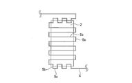
- FIG. 3 is a cross-sectional view taken along line III-III in FIG.
- FIG. 3 shows the structure of the detection circuit which detects the change of the resistance value of wiring.
- FIG. 7 is a cross-sectional view taken along line IX-IX of FIG. It is a top view by the side of a light extraction surface showing composition of an optical member concerning a 3rd embodiment. It is a bottom view of the holding member of FIG. It is a top view of the heat radiating member of FIG.
- FIG. 11 is a cross-sectional view taken along line XIII-XIII of FIG. It is sectional drawing which shows the modification of the optical member which concerns on 1st Embodiment.
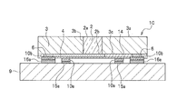
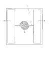
- the optical member 1A includes the conversion member 2, the holding member 3 and the wiring 4. Further, it is preferable that the optical member 1A includes the heat dissipation member 9.
- the light emitting device 20 preferably includes the optical member 1A and the laser element 25 and the package 21. More preferably, the light emitting device 20 includes the detection circuit 30.
- each component of the optical member 1A and the light emitting device 20 will be described.
- the conversion member 2 is a member having a first surface to be the light extraction surface 2 a and capable of converting laser light which is excitation light emitted from the laser element 25 into light of different wavelengths.
- the conversion member 2 has a surface opposite to the light extraction surface 2a (first surface) as a light irradiation surface 2b on which the laser beam from the laser element 25 is incident. Since the wiring 4 is formed on the light extraction surface 2a (first surface) which is the surface side of the conversion member 2, connection to an external power source or circuit for energizing the wiring 4 is facilitated.
- the conversion member 2 is preferably made of an inorganic material so as to be difficult to be decomposed by the irradiation of the laser beam.
- the conversion member 2 made of an inorganic material include ceramics or glass containing a phosphor capable of wavelength conversion of laser light, and a single crystal of a phosphor.
- the conversion member 2 is preferably a material having a high melting point, and the melting point is preferably 1300 to 2500 ° C. Since the conversion member 2 is formed of such a material having good light resistance and heat resistance, it is difficult to cause deterioration even when irradiated with high density light such as laser light, and is held by the holding member 3 Deformation and discoloration are less likely to occur due to heat during the process. Therefore, it is preferable that the conversion member 2 be formed of a material having good light resistance and heat resistance.
- cerium-activated yttrium aluminum garnet (YAG), cerium-activated lutetium aluminum garnet (LAG), europium and / or chromium-activated nitrogen-containing Examples include calcium aluminosilicate (CaO-Al 2 O 3 -SiO 2 ), europium-activated silicate ((Sr, Ba) 2 SiO 4 ), ⁇ -sialon phosphor, ⁇ -sialon phosphor, and the like.
- YAG which is a fluorescent substance having good heat resistance.
- a material obtained by sintering a phosphor and a translucent material such as aluminum oxide (Al 2 O 3 , melting point: about 1900 ° C. to 2100 ° C.) may be mentioned.
- the content of the phosphor is preferably 0.05 to 50% by volume, more preferably 1 to 30% by volume, with respect to the total volume of the ceramic.
- a ceramic substantially consisting of only a phosphor, which is formed by sintering a powder of a phosphor without using such a translucent material may be used as the conversion member 2.
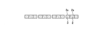
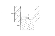
- the holding member 3 is a member which holds the conversion member 2 and has a surface 3 a (second surface) continuous on the same plane as the light extraction surface 2 a (first surface) of the conversion member 2.
- the holding member 3 has a through hole 3b penetrating in the thickness direction, and is connected to the conversion member 2 in a state where the conversion member 2 is inserted into the through hole 3b, thereby holding the conversion member 2 .
- the shape of the through hole 3 b is preferably made to correspond to the shape of the conversion member 2, and may be, for example, a pillar shape, a cone shape, a truncated cone, a truncated pyramid or a combination thereof. Besides polygons such as quadrilaterals, they may be circular or oval.
- the thickness of the holding member 3 is preferably 0.2 mm or more in consideration of the strength. Further, the thickness of the holding member 3 may be any thickness that can hold the conversion member 2 and is preferably 2.0 mm or less in order to suppress cost increase and increase in the height of the optical member 1A.
- the holding member 3 is a material that reflects the laser light and the fluorescence emitted by the phosphor with high reflectance, and is made of a material with high thermal conductivity that exhausts the heat of the conversion member 2 held in the through hole 3b.
- Materials having high reflectance and high thermal conductivity include light reflective ceramics, metals, or composites of ceramics and metals. It is preferable that it is light-reflective ceramics in which a high reflectance is easy to be obtained. It is preferable to use alumina (Al 2 O 3 ) ceramic as the light reflective ceramic.
- the wiring 4 is a linear body continuously formed from the light extraction surface 2 a (first surface) of the conversion member 2 to the surface 3 a (second surface) of the holding member 3.
- the wiring 4 is not limited to being formed directly on the surfaces of the conversion member 2 and the holding member 3, and may be formed via a film such as a light transmitting film 7 (see FIG. 14). Further, in plan view, the wiring 4 has a shape of one stroke.
- the wiring 4 is electrically connected to the conduction unit 6 for conduction at both ends thereof.
- the wiring 4 crosses the boundary between the conversion member 2 and the holding member 3 from the light extraction surface 2 a (first surface) of the conversion member 2 to the surface 3 a (second surface) of the holding member 3. Are formed continuously.
- the breakage of the wiring 4 is not limited to the disconnection of the wiring 4 but also includes partial or entire thinning or thinning due to chipping or the like.
- the resistance value of the wiring 4 is changed due to thinning or the like, and the voltage value is changed, so that the difference from the normal state can be known, and member damage can be detected.
- damage to the conversion member 2 and the holding member 3 in the vicinity of the boundary can be detected, it is possible to more accurately detect an abnormality that leads to a laser beam leak.
- the boundary between the members can be arranged at a position where the laser light easily hits. Can be reduced to achieve high brightness.
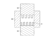
- the wiring 4 covers at least a part of the light extraction surface 2a (first surface) of the conversion member 2 and has a shape in which a part has a plurality of bending parts 5a in a plan view, and at least one of the plurality of bending parts 5a. Preferably, one is formed over the surface 3 a (second surface) of the holding member 3.
- the number and the pitch of the bent portions 5a in the bellows shape as shown in FIG. 2 are appropriately set in consideration of the size of the through holes 3b of the holding member 3 and the width of the wiring 4.
- the wiring 4 When the wiring 4 has a bellows shape, a plurality of locations where the wiring 4 straddles the boundary between the conversion member 2 and the holding member 3 will be set, and damage to the conversion member 2 and the holding member 3 in the vicinity of the boundary will be detected. Accuracy is improved. In other words, it can be said that the wiring 4 shown in FIGS. 1 to 3 has a shape having an extending portion 5b extending in one direction and a bending portion 5a connecting the adjacent extending portions 5b.
- the wiring 4 is made of a conductive material generally used as a wiring of the light emitting device 20.
- the wiring 4 is preferably made of a translucent conductive material in order to suppress a decrease in luminance of light extracted from the conversion member 2.
- ITO indium tin oxide
- the conducting portion 6 electrically connected at both ends of the wiring 4 can also be formed in a film shape using a conductive material.
- a metal layer such as a Ti / Pt / Au layer is provided on the ITO layer to improve the adhesion of the wire etc. It is preferable to do.
- the wiring 4 preferably has a thickness of 50 to 200 nm at least above the conversion member 2 in order to suppress uneven brightness of light extracted from the conversion member 2.
- the width of the wiring 4 is preferably 5 to 50 ⁇ m. If the thickness of the wiring 4 is less than 50 nm or the width is less than 5 ⁇ m, breakage such as disconnection easily occurs in the wiring 4 even if the conversion member 2 and the holding member 3 are not damaged, leading to erroneous detection of member breakage easy. In addition, when the thickness of the wiring 4 exceeds 200 nm or the width exceeds 50 ⁇ m, it becomes difficult to suppress the luminance unevenness of the light extracted from the conversion member 2.
- the heat radiating member 9 is a translucent member disposed on the back surface 3 c side of the holding member 3 and transmitting the laser beam from the laser element 25. It is preferable to use sapphire which is a light transmitting material having a high thermal conductivity as a main member constituting the heat dissipation member 9. By providing the heat dissipation member 9, the heat from the conversion member 2 can be efficiently dissipated.
- the thickness of the heat dissipation member 9 is, for example, 0.2 to 1 mm, preferably 0.4 to 0.6 mm.
- the first metal layer 10 and the second metal layer 11 can be used to join the heat dissipation member 9 and the holding member 3.
- the first metal layer 10 and the second metal layer 11 are made of a metal material containing at least one selected from gold, tin, silver, nickel, rhodium, aluminum, tungsten, platinum, titanium, ruthenium, molybdenum, niobium Is preferred.
- the first metal layer 10 and the second metal layer 11 are, for example, a laminated film made of a titanium film, a platinum film and a gold film, or a laminated film made of a mixed film made of a titanium film, a platinum film, a gold film and a gold-tin alloy. It is a membrane.
- the first metal layer 10 is formed on the holding member 3 side, and the second metal layer 11 is formed on the heat dissipation member 9 side.
- a gold-tin alloy is formed on either one of the first metal layer 10 and the second metal layer 11, the first metal layer 10 and the second metal layer 11 are brought into contact, and heating is performed to a temperature above the melting point of the gold-tin alloy. By doing this, the heat dissipating member 9 and the holding member 3 can be joined.
- the thickness of each of the first metal layer 10 and the second metal layer 11 can be, for example, 0.1 to 5 ⁇ m.
- the first metal layer 10 is made Ti (6 nm) / Pt (200 nm) / Au (300 nm) in order from the holding member 3 side
- the second metal layer 11 is in order from the heat dissipation member 9 side (6 nm) / Pt (200 nm) / Au (50 nm) / AuSn (3 ⁇ m) can be mentioned.
- joining members such as the first metal layer 10 and the second metal layer 11 are not formed at positions facing the conversion member 2.
- the laser beam is not blocked by the bonding member such as the first metal layer 10 or the like.
- the first metal layer 10 is formed to surround the light irradiation surface 2 b of the conversion member 2 facing the heat dissipation member 9. Therefore, the first metal layer 10 and the heat dissipation member 9 can effectively prevent the adhesion of dust to the light irradiation surface 2 b of the conversion member 2.
- the laser element 25 is arranged to irradiate the conversion member 2 with a laser beam.
- the laser element 25 has higher energy as the emitted laser beam has a shorter wavelength, and detection of a leak of the laser beam is more required. Therefore, it is preferable to use an element that emits a short wavelength laser beam as the laser element 25 .
- a laser element a semiconductor laser element made of a nitride semiconductor can be mentioned.
- the laser element 25 can be provided with a configuration for irradiating the conversion member 2 with the laser light, for example, the reflection member 26 in the optical path.
- the reflection member 26 a member in which a reflection film is provided on the slope of the main body made of glass or the like having a shape such as a triangular prism or a quadrangular pyramid can be used.
- the angle of the slope with respect to the bottom of the main body is preferably about 45 degrees in order to guide the laser light in the orthogonal direction.
- the package 21 encloses the laser element 25.
- the package 21 is a storage body having a storage portion such as the concave portion 27 and the like, in which the laser element 25 and the reflection member 26 are disposed and stored.
- the package 21 mainly includes a housing main body 22 made of a ceramic such as aluminum oxide, aluminum nitride, silicon nitride, silicon carbide or a metal such as Cu, and a lid 24 joined to the housing main body 22 by welding or the like.
- the storage body portion 22 can have a recess 27 opened on the upper surface side. At the periphery of the recess opening, a frame-shaped welding portion 23 containing iron as a main component for welding with the lid portion 24 may be provided.
- the storage body portion 22 is formed such that at least one surface of the upper surface continuous with the opening of the recess 27 is wider than the other surfaces, and the electrode portion 28 is disposed.
- the electrode part 28 may arrange
- a lead terminal is used as the electrode 28.
- the lid portion 24 hermetically seals the laser element 25 by being joined to the housing main portion 22 by welding or the like. Thereby, adhesion of dust such as organic matter to the laser element 25 can be suppressed.
- the lid portion 24 may have a support portion 24 a welded to the storage body portion 22, a light transmitting portion 24 b for transmitting a laser beam, and a bonding material 24 c for bonding the support portion 24 a and the light transmitting portion 24 b. it can.
- a material containing iron as a main component can be used for the support portion 24a. Glass, sapphire, etc. can be used for the light transmission part 24b. Low melting point glass, gold-tin solder or the like can be used as the bonding material 24c.
- the laser beam emitted from the laser element 25 is reflected by the reflection member 26, passes through the light transmitting portion 24 b and the heat dissipation member 9, and is irradiated to the light irradiation surface 2 b of the conversion member 2.
- the package 21 includes an electrode portion 28 exposed on the top surface of the storage body portion 22.
- the entire surface of the lower surface of the package 21 may be mounted on another member such as a heat sink by providing the electrode portion 28 electrically connected to the outside on the surface other than the lower surface of the storage main body 22. it can. Therefore, the package 21 easily dissipates the heat generated by the light emitting device 20 to the heat sink.
- the detection circuit 30 is a circuit that detects a change in resistance value caused by the breakage of the wiring 4.
- the light emitting device 20 is a circuit connected to the conductive circuit of the wiring 4 and the laser element 25.
- breakage of the conversion member 2 and the holding member 3 can be detected by a change in resistance value caused by breakage of the wiring 4. Then, when a change in the resistance value of the wiring 4 is detected, it is determined that the conversion member 2 and the holding member 3 are damaged, and the driving of the laser element 25 is stopped to prevent the leakage of the laser light. Can.
- the detection circuit 30 only needs to be able to detect the breakage of the wiring 4.
- the detection circuit 30 has a circuit configuration shown in FIG. As shown in FIG. 4, the detection circuit 30 detects a change in resistance value due to the breakage of the wiring 4 based on a change in voltage value.
- the detection circuit 30 includes a first connection conductor 31 and a second connection conductor 32.
- a power supply for conduction is connected to the first connection conducting wire 31, and the wiring 4, the laser element 25 and the switch element 33 are connected.
- a voltage detection resistor 34 is connected to the second connection wire 32.
- the wire 4 and the voltage detection resistor 34 are energized by the energizing power supply.
- the switch element 33 controls the driving stop of the laser element 25 by comparing the voltage of the voltage detection resistor 34 with the reference voltage.
- the resistance value of the wiring 4 is normally low and the voltage of the wiring 4 is low. Therefore, the voltage of the voltage detection resistor 34 is relatively high. It becomes above.
- the drive of the laser element 25 is continued according to the input from the switch element 33.
- the resistance of the wiring 4 is increased due to the breakage of the wiring 4, the voltage of the wiring 4 is increased, and the voltage of the voltage detection resistor 34 is relatively decreased.
- the drive of the laser element 25 is stopped.
- the switch element 33 an operational amplifier, a comparator, a bipolar transistor, a MOSFET (metal-oxide-semiconductor field-effect transistor) or the like can be used.
- a transistor element such as a MOSFET whose on / off can be controlled by the voltage of the voltage detection resistor 34 is preferable.
- the switch element 33 is, for example, a transistor element such as a MOSFET, and may be one that is turned on when the voltage of the voltage detection resistor 34 is equal to or higher than the reference voltage. As a result, when the voltage of the voltage detection resistor 34 decreases and becomes less than the reference voltage, the switch element 33 is turned off, and the current supply to the laser element 25 can be automatically stopped.
- the optical member 1A is fixed to the package 21 so that the laser light that has passed through the light transmitting portion 24b and the heat dissipation member 9 from the recess 27 reaches the conversion member 2. Then, it is preferable that the plurality of bent portions 5 a of the wiring 4 be arranged to straddle the boundary between the conversion member 2 and the holding member 3. With such an arrangement, breakage of the boundary between the conversion member 2 and the holding member 3 can be detected accurately by the wiring 4.
- the heat dissipating member 9 and the first metal layer 10 can be used to fix the optical member 1A to the package 21.
- the method of manufacturing an optical member includes (1) preparing a sintered body, and (2) removing a part of the conversion member and the holding member, And (3) including the step of forming a wiring. Each step will be described below.
- Step of Preparing a Sintered Body As shown in FIG. 5A, in the step of preparing a sintered body, the converting member 2 and the holding member 3 are brought into contact with each other to prepare an integrally formed sintered body 100. It is a process.
- the method of obtaining the sintered body 100 includes, for example, a step of preparing the conversion member 2, a step of forming a molded body to be the holding member 3, and a step of sintering the conversion member 2 and the molded body. The method is mentioned.
- a sintered body refers to a material obtained by heating a powdery material at a temperature lower than its melting point and hardening it.
- the conversion member 2 formed of a molded article and the holding member 3 of powder particles not yet sintered are heat-treated as in the present manufacturing method, the conversion member 2 formed of a molded article It is considered that a sintering phenomenon similar to a general sintering phenomenon has occurred on the surface and the surface of the holding member 3 of powder particles. Therefore, in this specification, what integrally formed the conversion member 2 which consists of molded articles, and the holding member 3 of powder particles is also called a sintered compact. Similarly, a member in which the powder particle conversion member 2 and the holding member 3 made of a molded product are integrally formed is also referred to as a sintered body.
- a sintering method for example, a discharge plasma sintering method (SPS method: spark plasma sintering method) or a hot press sintering method (HP method: hot pressing method) can be used.
- SPS method spark plasma sintering method
- HP method hot press sintering method
- the sintering temperature is preferably set to 1200 ° C. or more and 1800 ° C. or less, and more preferably set to 1400 ° C. or more and 1500 ° C. or less.
- the temperature is preferably set to 1200 ° C. or higher, the strength of the holding member 3 can be secured. Further, by setting the temperature to 1800 ° C. or less, the possibility that the light transmitting property of the holding member 3 becomes high can be reduced.
- the plurality of sintered bodies 100 are singulated so that one sintered body 100 includes one conversion member 2.
- a plurality of sintered bodies 100 can be singulated by using one or more of scribing, dicing, and breaking.
- one sintered body 100 is singulated so as to include one conversion member 2
- one sintered body 100 is singulated so as to include a plurality of conversion members 2. It is also good.
- Step of Forming Wiring This is a step of forming the wiring 4 continuously from the light extraction surface 2 a (first surface) of the conversion member 2 to the surface 3 a (second surface) of the holding member 3.
- Examples of the method for forming the wiring 4 include sputtering, chemical vapor deposition, and atomic layer deposition.
- the wiring 4 is continuously formed from the light extraction surface 2 a (first surface) of the conversion member 2 to the surface 3 a (second surface) of the holding member 3, the light extraction surface 2 a (first The breakage in the vicinity of the boundary between the surface) and the surface 3 a (second surface) of the holding member 3 can be detected by the breakage of the wiring 4. As a result, it is possible to detect an abnormality that leads to a laser beam leak more accurately.
- the method of manufacturing the optical member 1A includes, after the step of forming the wiring, a bonding step of bonding the heat dissipation member 9 and the holding member 3 using the first metal layer 10 formed by the sputtering method or the like.
- the optical member 1 B used for the light emitting device 20 includes the conversion member 2, the holding member 3, and the wiring 4. Moreover, it is preferable that the optical member 1B includes the heat dissipation member 9.
- the light emitting device 20 preferably includes the optical member 1 B and the laser element 25 and the package 21. As in the light emitting device 20 according to the first embodiment, the light emitting device 20 more preferably includes the detection circuit 30. The components of the optical member 1B and the light emitting device 20 will be described. The same as the optical member 1A and the light emitting device 20 shown in FIGS. 1 to 4 except for the matters described below.
- the light irradiation surface 2b on the back surface side of the conversion member 2 that is the heat dissipation member 9 side is the first surface.
- the wiring 4 is continuously formed across the boundary from the light irradiation surface 2 b (first surface) to the back surface 3 c (second surface) of the holding member 3. That is, the wiring 4 is disposed between the conversion member 2 and the holding member 3 and the heat dissipation member 9.
- the conversion member 2 has a surface opposite to the light irradiation surface 2b as a light extraction surface 2a from which the wavelength-converted light is emitted.
- the wavelength-converted light extracted from the conversion member 2 is not affected by the wiring 4, thereby reducing the uneven brightness. be able to.
- the 2nd metal layer 11 is used for joining of the holding member 3 and the thermal radiation member 9 in the optical member 1B.
- the first metal layer 10 includes the center-side first metal layer 10 a and the end-side first metal layer 10 b, and has a role of bonding the holding member 3 and the heat dissipation member 9.
- the constituent material and thickness of the center side first metal layer 10 a and the end side first metal layer 10 b are the same as those of the first metal layer 10 of the optical member 1 A.
- the center-side first metal layer 10a is a center of the back surface 3c (second surface) of the holding member 3 so as to surround the wiring 4 formed on the light irradiation surface 2b (first surface) surface of the conversion member 2 in plan view. Is formed in a rectangular ring shape.
- the central side first metal layer 10 a is electrically connected to the wiring 4, detection of breakage of the wiring 4 becomes difficult. Therefore, the central side first metal layer 10 a is insulated from the wiring 4 by being disposed through the wiring 4 and the insulating film 14. As the area where the central first metal layer 10a and the wiring 4 overlap in a plan view has a smaller area, the possibility of leakage between the central first metal layer 10a and the wiring 4 can be reduced. For this reason, as shown in FIG. 7, it is preferable to place the central first metal layer 10a and the wiring 4 in only two places in plan view. In order to achieve such an arrangement, the central side first metal layer 10 a may be arranged outside the bent portion 5 a of the wiring 4.
- the end-side first metal layer 10b is formed in a rectangular shape on the left and right, respectively, separated from the center of the back surface 3c on which the center-side first metal layer 10a is formed so as to cover the two conducting parts 6 for energizing the wiring 4. It is done.
- the two end-side first metal layers 10 b are electrically connected to the wiring 4, respectively, and serve as the anode and the cathode of the wiring 4.
- the second metal layer 11 includes a center-side second metal layer 11 a and an end-side second metal layer 11 b.
- the constituent material and thickness of the center side second metal layer 11a and the end side second metal layer 11b are the same as those of the second metal layer 11 of the optical member 1A.
- the central second metal layer 11a is formed on the central side of the surface of the heat dissipation member 9 facing the holding member 3 so as to cover the central first metal layer 10a formed on the back surface 3c (second surface). There is.
- the center-side second metal layer 11 a is formed in a rectangular ring shape so as to surround the wiring 4 in the same manner as the center-side first metal layer 10 a.
- the end-portion-side second metal layer 11 b is formed in a rectangular shape on the left and right of the surface of the heat dissipation member 9 facing the holding member 3 while being separated from the center-side second metal layer 11 a.
- the end-portion-side second metal layer 11 b is formed in a rectangular shape having a size such that a part thereof protrudes outward from the holding member 3 in plan view when the holding member 3 and the heat dissipation member 9 are joined.
- the two end-side second metal layers 11 b are electrically connected to the current-carrying portions 6 (end-side first metal layers 10 b), respectively, in addition to the bonding of the holding member 3 and the heat dissipation member 9. It has a role of supplying electricity from the outside to the conduction part 6 of the above.
- the end-portion-side second metal layer 11 b is arranged so that a portion thereof is exposed from the holding member 3 in plan view after bonding. Thereby, a wire etc. can be connected to the part exposed from the holding member 3.
- the end-side second metal layer 11b can be easily pulled out by disposing the end-side second metal layer 11b connected to the outside outside the center-side second metal layer 11a.
- the center-side first metal layer 10 a and the center-side second metal layer 11 a are formed together with the heat dissipation member 9 so as to surround the light irradiation surface 2 b (first surface) of the conversion member 2. Therefore, it is possible to effectively prevent the adhesion of dust to the light irradiation surface 2 b (first surface) of the conversion member 2.
- the planar view shape of the center side 1st metal layer 10a and the center side 2nd metal layer 11a is cyclic
- the insulating film 14 is a film that insulates the central side first metal layer 10 a and the wiring 4.
- the insulating film 14 is disposed at least in a portion where the central first metal layer 10 a and the wiring 4 overlap in a plan view. In the case where the insulating film 14 is also disposed on the path of the laser light, the insulating film 14 is preferably translucent.
- the insulating film 14 is a light irradiation surface 2b (first surface) of the conversion member 2 excluding the region where the two conducting parts 6 for energizing the wiring 4 are formed, the back surface 3c (second surface) of the wiring 4 and the holding member 3 Can be formed to cover the whole of.
- the insulating film 14 may double as the protective film 8 in the modification of the first embodiment described later.
- the constituent material and thickness can be the same as that of the protective film 8.
- the light emitting device 20 is different from the light emitting device 20 in that the optical member 1B is used instead of the optical member 1A. It is the same as that of one embodiment.
- the light emitting device 20 having such a configuration can reduce the luminance unevenness of the extracted light by using the optical member 1B.
- the optical member 1B can be manufactured by the same manufacturing method as that of the first embodiment.
- the optical member 1B manufactures the light irradiation surface 2b of the conversion member 2 as a 1st surface in which the wiring 4 is formed.
- the central first metal layer 10a and the end first metal layer 10b formed by sputtering or the like, and the central second metal layer 11a are included.
- an optical member 1C according to the third embodiment has a part of the optical member 1B according to the second embodiment modified. That is, in the optical member 1C, the second metal layer on the center side of the second metal layer 11 is changed in shape so that a part thereof is exposed from the holding member 3 in a plan view, and becomes the leak checking electrode 15.
- the optical member 1 ⁇ / b> C includes the conversion member 2, the holding member 3, the wiring 4, the first metal layer 10, the insulating film 14, the leak check electrode 15, the wiring electrode 16, and the heat dissipation member 9.
- the light emitting device 20 preferably includes the optical member 1C and the laser element 25 and the package 21. More preferably, the light emitting device 20 includes the detection circuit 30. Each component of the optical member 1C will be described. The same as the optical member 1B shown in FIGS. 6 to 9 except for the matters described below.
- the leak check electrode 15 includes a central portion 15a and a terminal portion 15b connected to the central portion 15a via a linear connection portion 15c.
- the leak checking electrode 15 is used to check whether insulation between the central first metal layer 10 a and the wiring 4 can be secured after the holding member 3 and the heat radiating member 9 are joined.
- the leak check electrode 15 is electrically connected to the central first metal layer 10a.
- the terminal portion 15b of the leak check electrode 15 is used as an anode, a voltage is applied between the leak check electrode 15 and the cathode side of the wiring electrode 16, and it is checked whether current flows or not. And it can be determined whether the wiring 4 is leaking.
- the anode and the cathode may be reversed.
- the central portion 15a is formed in a rectangular ring shape on the heat dissipation member 9 side so as to cover the central first metal layer 10a formed so as to surround the conversion member 2 (first surface) in plan view.
- the central portion 15a can be formed to have the same size as the central first metal layer 10a.
- the terminal portion 15b is electrically connected to the outside, when the holding member 3 and the heat dissipation member 9 are joined, the terminal portion 15b is formed in such a size and position that a part thereof protrudes outward from the holding member 3 in plan view. ing.
- the terminal portion 15b is electrically connected to the central portion 15a via the connection portion 15c.
- the terminal portion 15 b is formed on the heat dissipation member 9 side in a rectangular shape along one side of the heat dissipation member 9.
- the central portion 15a, the connection portion 15c, and the terminal portion 15b correspond to the central second metal layer 11a in the optical member 1B, and the constituent material and thickness are the same as those of the central second metal layer 11a in the optical member 1B. It can be done.
- the central portion 15 a, the connection portion 15 c, and the terminal portion 15 b are also used to join the holding member 3 and the heat dissipation member 9.
- the wiring electrode 16 corresponds to the end-side second metal layer 11b in the optical member 1B, and the shape is different only from the end-side second metal layer 11b, and the constituent material and the thickness are the same. be able to.
- the wiring electrode 16 includes a central portion 16a and a terminal portion 16b connected to the central portion 16a via a linear connection portion 16c.
- the central portion 16a has the same size as the end-side first metal layer 10b in order to electrically connect to the two current-carrying portions 6 via the end-side first metal layer 10b to energize the wiring 4.
- the heat dissipation member 9 is formed in a rectangular shape on the side.
- the terminal portion 16b When joining the holding member 3 and the heat radiation member 9, the terminal portion 16b has a rectangular shape at a corner portion of the heat radiation member 9 so as to have a size and a position in which a part protrudes outward from the holding member 3 in plan view. It is formed.
- the central portion 16a and the terminal portion 16b are formed to be electrically connected via the connection portion 16c.
- the central portion 16 a, the connection portion 16 c, and the terminal portion 16 b are also used to join the holding member 3 and the heat dissipation member 9.
- the light emitting device 20 is the same as the second embodiment except that an optical member 1C is used instead of the optical member 1B in the light emitting device 20 (see FIG. 9) using the optical member 1B of the second embodiment.
- the insulating film 14 is a film similar to the protective film 8 (see FIG. 14).
- the leak check electrode 15 central portion 15a and terminal portion 15b is a bonding layer similar to the central second metal layer 11a and the end second metal layer 11b (see FIGS. 8 and 9).
- the optical member 1C can be manufactured by the same manufacturing method as that of the second embodiment.
- the electrode 15 for checking leakage center portion A bonding step may be included in which the heat dissipation member 9 and the holding member 3 are bonded by using the connection portion 15c and the terminal portion 15b) and the wiring electrode 16 (the central portion 16a, the connection portion 16c and the terminal portion 16b).
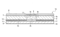
- an optical member 1 D which is a modification of the optical member 1 A according to the first embodiment, includes the conversion member 2, the holding member 3, the wiring 4, the translucent film 7, and the protective film 8. And a heat dissipation member 9, a dielectric multilayer film 17, and an antireflective film 18.
- the optical member 1D may include one or more of the translucent film 7, the protective film 8, the dielectric multilayer film 17, and the antireflection film 18.
- the conversion member 2, the holding member 3, the wiring 4, and the heat dissipation member 9 of the optical member 1D are the same as those of the optical member 1A, and thus the description thereof is omitted.
- the translucent film 7, the protective film 8, the dielectric multilayer film 17 and the antireflective film 18 of the optical member 1D will be described below.
- the translucent film 7 is a film that covers the light extraction surface 2 a (first surface) of the conversion member 2 and the surface 3 a (second surface) of the holding member 3.
- the flatness of the surfaces of the conversion member 2 and the holding member 3 can be improved.
- the wiring 4 is not directly formed on the surfaces of the conversion member 2 and the holding member 3 but is formed on the surface of the light transmitting film 7. Therefore, since the wiring 4 is formed on the surface of the light transmitting film 7 in which the flatness of the surface is improved more than the conversion member 2 and the holding member 3, the possibility of disconnection of the wiring 4 at the time of formation is reduced. it can.
- the conversion member 2 is made of two or more kinds of materials, if the surface of the conversion member 2 is subjected to a planarization process such as CMP, the removal rate is different depending on the material, and thus a level difference easily occurs on the surface. For this reason, it is preferable to form the translucent film 7 on the surface of the conversion member 2. Similarly, even when the holding member 3 is formed of light-reflecting ceramic, the ceramic tends to have a higher porosity as it is highly reflective, and the flatness of the surface of the holding member 3 is poor. Preferably, the light transmitting film 7 is formed.
- the translucent film 7 is made of a translucent material.
- a translucent material which is translucent to visible light a material containing silicon oxide such as SiO 2 may be mentioned.
- the translucent film 7 is, for example, a SiO 2 film.
- the thickness of the light transmitting film 7 is preferably such that the flatness of the conversion member 2 and the holding member 3 can be improved, and specifically, it is preferably 1 to 15 ⁇ m.
- the light transmitting film 7 may be formed to cover the light irradiation surface 2 b of the conversion member 2 and the back surface 3 c of the holding member 3.
- the protective film 8 is a translucent film formed so as to cover at least the light extraction surface 2 a (first surface) of the conversion member 2 and the wiring 4.
- the protective film 8 is formed to cover the entire light extraction surface 2a (first surface).
- the wiring 4 can be protected so that the wiring 4 is not damaged by a slight impact that does not damage the conversion member 2.
- the thickness of the protective film 8 is, for example, not less than the wavelength of excitation light (for example, 450 nm) and not more than 20 ⁇ m.
- the protective film 8 is made of a translucent material in the same manner as the translucent film 7.
- a translucent material which is translucent to visible light a material containing silicon oxide such as SiO 2 may be mentioned.
- the protective film 8 is, for example, a SiO 2 film.
- the refractive index of the protective film 8 be a value close to the refractive index of the wiring 4 and the protective film 8 be disposed at least in a region where the wiring 4 is not formed. Thereby, the difference in refractive index between the region in which the wiring 4 is formed and the region in which the wiring 4 is not formed can be reduced, and unevenness in luminance can be reduced.
- the protective film 8 preferably contains silicon oxide and a material having a refractive index higher than silicon oxide. As described above, when the protective film 8 contains a material having a high refractive index, the uneven brightness can be improved as described above. Specifically, for the protective film 8, it is preferable to use a material in which a predetermined amount of tantalum oxide is mixed with silicon oxide.
- the protective film 8 can be, for example, a film in which SiO 2 and Ta 2 O 5 are mixed. If the wiring 4 is ITO, the protective film 8, SiO 2 is suitable to be a mixed film of SiO 2 and Ta 2 O 5 of about 25 to 35 wt%.
- the dielectric multi-layered film 17 is a multi-layered film disposed on the top surface of the heat dissipating member 9 on the side of the conversion member 2 and the holding member 3.
- the dielectric multilayer film 17 is formed by laminating, for example, two or more dielectric films having different refractive indexes, which are made of a dielectric such as aluminum nitride, silicon oxide, aluminum oxide, zirconium oxide, titanium oxide, niobium oxide or tantalum oxide. It is
- the dielectric multilayer film 17 is a film that transmits the laser light from the laser element 25 and reflects wavelength conversion light from the light irradiation surface 2 b of the conversion member 2.
- the dielectric multilayer film 17 is a film that has a higher reflectance to the light wavelength-converted by the conversion member 2 than to the excitation light (laser light from the laser element 25). As a result, the light traveling from the conversion member 2 toward the laser element 25 can be reflected back to the conversion member 2, so that the light extraction efficiency from the light extraction surface 2 a of the conversion member 2 can be improved.
- the thickness of the dielectric multilayer film 17 can be, for example, 1 to 10 ⁇ m.
- the anti-reflection film 18 is a film disposed on the lower surface which is the surface of the heat radiation member 9 on which the laser light is incident.
- the antireflective film 18 is made of, for example, a dielectric material mainly composed of at least one selected from aluminum nitride, silicon oxide, aluminum oxide, zirconium oxide, titanium oxide, niobium oxide, and tantalum oxide.
- the antireflective film 18 is a film having a very small value, such as 1% or less, of the reflectance to the laser light from the laser element 25 by adjusting the thickness, the composition ratio, and the like. By providing the anti-reflection film 18, it is possible to increase the amount of incident laser light to the conversion member 2.
- the thickness of the antireflective film 18 can be, for example, 0.2 to 1 ⁇ m.
- an optical member 1E which is a modification of the optical member 1B according to the second embodiment, includes the conversion member 2, the holding member 3, the wiring 4, the translucent film 7, and the heat dissipation member 9. And a dielectric multilayer film 17 and an antireflective film 18.
- an optical member 1F which is a modification of the optical member 1C according to the third embodiment, includes the conversion member 2, the holding member 3, the wiring 4, the light transmitting film 7 and the heat dissipation member 9, the dielectric multilayer film 17, and the antireflective film 18.
- the light transmitting film 7, the protective film 8, the dielectric multilayer film 17, and the antireflection film 18 can be provided.
- the conversion member 2, the holding member 3, the wiring 4, and the heat dissipation member 9 of the optical members 1E and 1F are the same as those of the optical member 1B.
- the translucent film 7, the dielectric multilayer film 17, and the anti-reflection film 18 of the optical members 1E and 1F are the same as those of the optical member 1D.
- the translucent films 7 of the optical members 1E and 1F are formed to cover the light irradiation surface 2b (first surface) of the conversion member 2 and the back surface 3c (second surface) of the holding member 3.
- the translucent film 7 covering the surface on which the wiring 4 is provided (that is, the light irradiation surface 2 b and the back surface 3 c), as described above, the possibility of the wiring 4 breaking during formation is reduced.
- the light transmitting film 7 may be formed to cover the light extraction surface 2 a of the conversion member 2 and the surface 3 a of the holding member 3.
- FIG. 17A Showe of wiring
- a part of the spiral-shaped portion of the wiring 4 covers the conversion member 2, and another part is formed on the holding member 3.
- the number of turns and the pitch in the spiral shape are appropriately set in consideration of the size of the through hole 3 b of the holding member 3 and the width of the wiring 4.
- the wiring 4 has a bellows shape as shown in FIG. 2, for example, if a crack extending in the lateral direction in the drawing is generated in the conversion member 2, the conversion member 2 is broken but the wiring 4 is not broken. obtain.
- the wiring 4 is broken and it is possible to detect an abnormality, regardless of whether it is a crack in the horizontal direction or a crack in the vertical direction in the drawing.
- the pitch of the spiral shape be 60 ⁇ m or less.
- the pitch of the spiral shape is, in other words, the width of the passage portion which is a portion where the wiring 4 is not provided.
- the pitch of the spiral shape is preferably 5 ⁇ m or more so that the passage portion is not crushed when the wiring 4 is formed.
- the wiring 4 shown by each embodiment and modification is a shape which the extending
- the allowance of the shift in the width direction of the stretched portion 5b is equal to or less than the width of the outermost stretched portion 5b, and when shifted more than that, the outermost stretched portion 5b is the conversion member 2 And does not overlap with the boundary between
- FIG. 17B the wiring 4 shown by each embodiment and modification is a shape which the extending
- the misalignment is permitted.
- the capacitance can be made larger than the width of the wiring 4.
- the respective extending portions 5b are connected by the bending portion 5a, whereby the wiring 4 has a single-stroke writing shape.
- the wiring 4 shown in each of the embodiments and the modifications intersects with any of the sides forming the outer edge of the conversion member 2. It may be a one-stroke writing shape having a plurality of stretched portions 5b to be stretched and a bent portion 5a connecting the adjacent stretched portions 5b.
- the extension direction of the portion other than the bending portion 5a in the wiring 4 overlapping the conversion member 2 is only one direction, the allowable amount of deviation of the wiring 4 with respect to the boundary between the conversion member 2 and the holding member 3 is shown in FIGS. It can be expanded more than the case of the wiring 4 shown.
- the bending part 5a is formed in linear form, curvilinear forms, such as semicircle, may be sufficient.
- the stretched portion 5b is also formed in a linear shape, it may have a shape other than the linear shape, such as repeating the unevenness of the straight line or repeating the unevenness of the curve.
- the modified example of the method of manufacturing the optical member 1A of the first embodiment includes (1) preparing a sintered body, (2) removing a part of the conversion member and the holding member, and (A) heat treating And (B) forming a light-transmissive film, and (3) forming a wiring.
- the steps (1) to (3) are the same as the above-described manufacturing method, and thus the description thereof is omitted.
- the steps (A) and (B) will be described below.
- the same modification can be adopted in the method of manufacturing the optical members 1B and 1C according to the second and third embodiments.
- the residual organic matter is produced by heating the holding member 3 in a state where at least a part of the route through which the organic matter escapes is blocked by the wiring 4 or the like in a later step. It becomes black and causes the appearance abnormality of the holding member 3 to occur. Therefore, by performing the heat treatment before forming the wiring 4 and the like, the residual organic substance in the holding member 3 can be reduced, and the possibility of the appearance abnormality of the holding member 3 can be reduced.
- the temperature of the heat treatment is preferably lower than the sintering temperature of the sintered body constituting the holding member 3. This can reduce the possibility of shrinkage, warpage, and the like of the material due to re-sintering of the sintered body due to the heat treatment.
- the temperature of the heat treatment is preferably 1200 ° C. or less.
- the light extraction surface 2 a (first surface) of the heat treated conversion member 2 and the holding member 3 The light transmitting film 7 is formed to cover the surface 3a (second surface) of The translucent film 7 can be formed by a sputtering method, a chemical vapor deposition method, an atomic layer deposition method or the like.
- the formation of the light transmitting film 7 may be performed on the light irradiation surface 2b opposite to the first surface of the conversion member 2 and the back surface 3c opposite to the second surface of the holding member 3 after heat treatment. .
- the formation of the light transmitting film 7 can prevent the organic matter from infiltrating into the voids of the material forming the holding member 3 again. Therefore, the possibility of the appearance abnormality of the holding member 3 due to the blackening of the residual organic matter can be reduced.
- the light transmitting film 7 preferably has a large thickness in order to prevent re-penetration of an organic substance, and preferably can cover the surface of the holding member 3 without any gap. For this reason, it is preferable that the light transmitting film 7 be deposited first by the chemical vapor deposition method and then deposited by the atomic layer deposition method.
- the translucent film 7 is formed by first forming a 5 ⁇ m thick SiO 2 film by a chemical vapor deposition method, and then forming a 1 ⁇ m thick SiO 2 / Al 2 O 3 multilayer film by an atomic layer deposition method. Further, as described above, the flatness of the surfaces of the conversion member 2 and the holding member 3 is improved by the formation of the light transmitting film 7, so that the possibility of breakage of the wiring 4 at the time of formation can be reduced.
- the method of manufacturing an optical member according to the first embodiment after the step of forming the wiring 4, before the step of arranging the heat dissipation member 9, light extraction in which the translucent film 7 is formed as shown in FIG.
- the method may further include the step of forming the protective film 8 by a sputtering method, a chemical vapor deposition method, an atomic layer deposition method or the like so as to cover the surface 2 a and the wiring 4.
- the step of manufacturing the optical member according to the second and third embodiments after the step of forming the wiring 4 and before the step of arranging the heat dissipation member 9, as shown in FIGS.
- the method may further include the step of forming the insulating film 14 by a sputtering method, a chemical vapor deposition method, an atomic layer deposition method, or the like so as to cover the light irradiation surface 2 b on which the is formed and to cover the wiring 4.
- the sintered body may be obtained by the following first to third manufacturing methods.
- the following first to third manufacturing methods will be described by way of example of manufacturing the optical member 1A in which the light extraction surface 2a of the conversion member 2 is the first surface on which the wiring 4 is formed.
- the terms "powdery conversion member” and “conversion member made of sintered body” are used, and in the case of the conversion member, the terms are used.
- conversion member is used.
- bindery holding member and “holding member made of sintered body” are used, and in the case of a holding member Regardless of the term “holding member” is used.
- Step of obtaining a sintered body As shown in FIGS. 18A to 18C, in the step of obtaining a sintered body, the conversion member 2 and the holding member 3 are brought into contact to obtain a sintered body 100 integrally formed. It is a process. Specifically, the method includes a step of preparing the conversion member 2, a step of arranging the holding member 3, and a step of obtaining the sintered body 100.
- a powdery material for example, the same material as the holding member 3) as a buffer member 70 before the step of preparing the conversion member 2 Place.
- the sintering die 80 and the lower punch 90 are used as a container.
- the buffer member 70 is not essential, it is preferable to use the buffer member 70. Thereby, even when the conversion member 2 made of a sintered body is used, the pressure applied to the conversion member 2 can be made substantially even when the holding member 3 (see FIG. 18C) is sintered later. . Therefore, the crack etc. of the conversion member 2 which consists of sintered compacts can be reduced.
- the release sheet 60 is disposed above the buffer member 70.
- a polyethylene sheet or a carbon sheet can be used as the release sheet 60.
- a powdery phosphor and a material same as the holding member 3 in a region surrounded by the lower punch 90 provided with the buffer member 70 and the release sheet 60 and the sintering die 80. And sintering a powder obtained by mixing a powdery sintering aid and a plate-like sintered body. Furthermore, a plurality of convex portions are formed on the plate-like sintered body using a machining center, and the conversion member 2 formed of the sintered body having the plurality of convex portions provided on the upper surface side is obtained.
- the powdery holding member 3 is placed between the plurality of convex portions in the conversion member 2.
- the holding member 3 can be easily filled between the adjacent convex portions, and the gap between the conversion member 2 and the holding member 3 can be substantially eliminated.
- the conversion member 2 is disposed such that the convex portion faces upward, and the holding member 3 is disposed between the convex portions of the conversion member 2 by arranging the powdery holding member 3 from above. There is.
- positioning can also be reversed. That is, first, the powdery holding member 3 is disposed in the container, and then the conversion member 2 made of a sintered body is disposed above the holding member 3 with the convex portion facing downward, and may be pressed as necessary. it can. Also in this case, the holding member 3 can be disposed between the plurality of convex portions in the conversion member 2.
- the sintered body 100 is preferably heat-treated in an oxidizing atmosphere (for example, the air atmosphere) in a range of 1000 ° C. or more and 1500 ° C. or less.
- an oxidizing atmosphere for example, the air atmosphere
- the second method for producing a sintered body will be described.
- the second manufacturing method of the sintered body is substantially the same as the items described in the first manufacturing method except for the matters described below, but the powdery conversion member and the powdery holding member are sintered. It differs from the first manufacturing method in that it is connected. Each step will be described below.
- Step of obtaining a sintered body As shown in FIGS. 19A to 19D, in the step of obtaining a sintered body, the converting member 2 and the holding member 3 are brought into contact to obtain a sintered body 100 integrally formed. It is a process. Specifically, the method includes the steps of preparing the holding member 3, disposing the conversion member 2, and obtaining the sintered body 100.
- Step of Preparing Holding Member A holding member 3 having a plurality of recesses provided on the top surface is prepared.
- the step of preparing the holding member 3 includes the step of filling the powdery holding member 3 in the container (the lower punch 90 and the sintering die 80) to be the sintering type (see FIG. 19A); Manufacturing the holding member 3 provided with a plurality of concave portions or convex portions by pressing the powdery holding member 3 with the pressing member 92 provided with the convex portions or concave portions (see FIG. 19B); including.
- the holding member 3 made of a sintered body may be prepared.
- Step of arranging conversion member A powdery conversion member 2 containing a phosphor is prepared. And the powdery conversion member 2 is arrange
- positioning of the holding member 3 and the conversion member 2 is not limited. That is, the holding member 3 made of a sintered body may be disposed below and the powdery conversion member 2 may be disposed above, or the order of the placement may be reversed.
- both the powdery conversion member 2 and the powdery holding member 3 are sintered to convert the conversion member 2 and the holding member 3 as shown in FIG. 19D.
- a sintered body 100 integrally formed.
- both the powdery conversion member 2 and the powdery holding member 3 are sintered to obtain a sintered body 100.
- the 3rd manufacturing method of a sintered compact is explained.
- the third manufacturing method of the sintered body is substantially the same as the items described in the second manufacturing method except for the matters to be described next, but the upper surface side is only composed of the conversion member and the lower surface side is the conversion member and holding It differs from the second manufacturing method in that a sintered body composed of members is obtained. Each step will be described below.
- Step of obtaining a sintered body As shown in FIGS. 20A to 20D, in the step of obtaining a sintered body, the conversion member 2 and the holding member 3 are brought into contact to obtain a sintered body 100 integrally formed. It is a process. Specifically, the method includes the steps of preparing the holding member 3, disposing the conversion member 2, and obtaining the sintered body 100.
- the holding member 3 is provided in the form of powder provided with a plurality of through holes penetrating the thickness of the installed holding member 3 but having a fixed shape (FIG. 20A) , B). In this step, the holding member 3 made of a sintered body may be prepared.
- Step of arranging conversion member A powdery conversion member 2 containing a phosphor is prepared. And the powdery conversion member 2 is arrange
- both the powdery conversion member 2 and the powdery holding member 3 are sintered to convert the conversion member 2 and the holding member 3 as shown in FIG. 20D.
- FIG. 21A it is a process of obtaining the fixed body which the conversion member 2 and the holding member 3 were integrated. Specifically, the process of forming the glass film 12 and the process of fixing the conversion member 2 are included.
- the glass film 12 is formed on the inner wall surface of the through hole 3 b formed in the holding member 3 or on the surface of the inner wall surface and the upper surface of the holding member 3 It is.
- the formation method of the through-hole 3b to the holding member 3 can use the conventionally well-known drilling method.
- the size of the through hole 3 b is appropriately set according to the size of the conversion member 2.
- the glass film 12 is formed by sputtering or the like.
- the thickness of the glass film 12 can be 0.1 to 20 ⁇ m.
- the thickness of the glass film 12 is less than 0.1 ⁇ m, a portion where the glass film 12 is not formed is easily formed on the inner wall surface of the through hole 3b, and the holding power of the conversion member 2 is easily reduced in the manufactured optical member.
- the thickness of the glass film 12 exceeds 20 ⁇ m, the absorption of light by the glass film 12 is increased, and the light emission efficiency of the optical member is easily reduced.
- the softening point of the glass film 12 be lower than that of the conversion member 2 and the holding member 3 in order to perform heat fusion.
- Step of Fixing Conversion Member The step is a step of fixing the conversion member 2 to the holding member 3 via the glass film 12.
- the conversion member 2 is placed on the holding member 3 through the glass film 12 by disposing the conversion member 2 in the through hole 3b in which the glass film 12 is provided on the inner side of the hole and heating the glass film 12 at the first atmosphere temperature. It is a process of obtaining the fixed fixed body.
- the first atmosphere temperature is appropriately set so that the glass film 12 can be deformed and thermally fused.
- the glass film 12 formed on the inner wall surface is solid at room temperature, but softened by heating and hardened by returning to room temperature again. Thereby, the conversion member 2 disposed in the through hole 3 b can be fixed to the holding member 3 without a gap.
- Step (2) Step of Removing a Portion of the Glass Film As shown in FIG. 21B, in the step, the upper surface side of the fixed body is removed by grinding, polishing, CMP or the like. In this step, it is preferable to remove the glass film 12 until the surface on the upper surface side of the holding member 3 is exposed. Thereby, a first surface to be a light irradiation surface or a light extraction surface of the conversion member 2 and a second surface of the holding member 3 continuous from the first surface are obtained. By thus fixing the conversion member 2 to the holding member 3 without a gap, it is possible to obtain a surface on which the wiring 4 can be formed. Note that this step may be omitted. In the present manufacturing method, the step (3) of forming a wiring is the same as the manufacturing method of the first to third embodiments.
- the light extraction surface of the conversion member 2 may be covered using a glass that softens like the glass film 12. Except for the above-described steps, the same steps and the like as in the first to third embodiments can be employed.
- Optical member 2 conversion member 2 a light extraction surface 2 b light irradiation surface 3 holding member 3 a front surface 3 c back surface 4 wiring 5 a bending portion 5 b extending portion 7 translucent film 8 protective film 9 heat dissipation member Reference Signs List 20 light emitting device 21 package 25 laser element 30 detection circuit
Abstract
Provided is an optical member (1A) comprising: a conversion member (2) that has a first face that becomes a light extraction surface (2a) and that can convert laser light that is excitation light into light of different wavelengths; a holding member (3) that holds the conversion member (2) and has a second face that is contiguous to the first face; and a linear wiring (4) that is formed contiguously from the first face to the second face.
Description
本開示は、光学部材、発光装置及び光学部材の製造方法に関するものである。
The present disclosure relates to an optical member, a light emitting device, and a method of manufacturing an optical member.
従来、レーザ素子を使った発光装置が知られている。このような発光装置では、レーザ光が当たる蛍光体板表面に導電性細線又は導電性線路を形成することで、蛍光体板のクラック等を検知し、レーザ光の漏れの防止を図っている(例えば、特許文献1、2参照)。
Conventionally, a light emitting device using a laser element is known. In such a light emitting device, a crack or the like of the phosphor plate is detected by forming a conductive thin line or a conductive line on the surface of the phosphor plate to which the laser light is applied to prevent the laser light from leaking ( See, for example, Patent Documents 1 and 2).
しかしながら、このような発光装置においては、蛍光体板のクラック等の検出は可能であるが、蛍光体板とその保持部材との境界部近傍でのクラック等の検出は困難である。また、発光装置の使用中に蛍光体板がずれたとしても、導電性細線又は導電性線路を外部回路と電気的に接続するためのワイヤ等が断線しない程度のズレであれば、異常と検出されない。これらの理由から、レーザ光の漏れ防止が不十分であるという問題があった。
However, in such a light emitting device, although detection of cracks and the like of the phosphor plate is possible, detection of cracks and the like in the vicinity of the boundary between the phosphor plate and the holding member is difficult. In addition, even if the phosphor plate shifts during use of the light emitting device, if it is a shift that does not break the wire or the like for electrically connecting the conductive thin line or conductive line to the external circuit, it is detected as abnormal. I will not. For these reasons, there is a problem that the laser beam leak prevention is insufficient.
そこで、本開示に係る実施形態は、レーザ光の漏れに繋がる異常をより精度良く検出可能である光学部材、光学部材を用いた発光装置及び光学部材の製造方法を提供することを課題とする。
Therefore, an embodiment according to the present disclosure has an object to provide an optical member capable of detecting an abnormality leading to a leak of laser light with high accuracy, a light emitting device using the optical member, and a method of manufacturing the optical member.
上記課題を解決するために、本開示の実施形態に係る光学部材は、光照射面又は光取出面となる第1面を有し、励起光であるレーザ光を異なる波長の光に変換可能である変換部材と、前記変換部材を保持し、前記第1面と連続する第2面を有する保持部材と、前記第1面から前記第2面にかけて連続して形成された線状の配線と、を備える。
In order to solve the above-mentioned subject, an optical member concerning an embodiment of this indication has the 1st field used as a light irradiation side or a light extraction side, and can convert laser light which is excitation light into light of a different wavelength, A conversion member, a holding member holding the conversion member and having a second surface continuous with the first surface, and a linear wiring continuously formed from the first surface to the second surface, Equipped with
本開示の実施形態に係る発光装置は、前記光学部材と、前記変換部材の前記光照射面にレーザ光を照射するように配置されるレーザ素子と、を備える。
A light emitting device according to an embodiment of the present disclosure includes: the optical member; and a laser element arranged to emit a laser beam to the light irradiation surface of the conversion member.
本開示の実施形態に係る光学部材の製造方法は、変換部材と保持部材とが一体に形成された焼結体を準備する工程と、前記変換部材の第1面と、前記第1面から連続する前記保持部材の第2面と、が得られるように、前記変換部材及び前記保持部材の一部を除去する工程と、前記第1面から前記第2面に連続して線状の配線を形成する工程と、を含む。
In a method of manufacturing an optical member according to an embodiment of the present disclosure, a step of preparing a sintered body in which a conversion member and a holding member are integrally formed, the first surface of the conversion member, and the first surface are continuous. Removing a portion of the conversion member and the holding member so as to obtain a second surface of the holding member, and a linear wiring continuously from the first surface to the second surface. And forming.
本開示の実施形態に係る光学部材及び発光装置によれば、レーザ光の漏れに繋がる異常をより精度良く検出することができる。本開示の実施形態に係る光学部材の製造方法によれば、レーザ光の漏れに繋がる異常をより精度良く検出可能な光学部材を製造することができる。
According to the optical member and the light emitting device according to the embodiment of the present disclosure, it is possible to more accurately detect the abnormality that leads to the leak of the laser light. According to the method of manufacturing an optical member according to the embodiment of the present disclosure, it is possible to manufacture an optical member capable of detecting an abnormality that leads to a leak of laser light with higher accuracy.
本開示の実施形態を、以下に図面を参照しながら説明する。但し、以下に示す形態は、本実施形態の技術思想を具現化するための光学部材及び発光装置を例示するものであって、以下に限定するものではない。また、実施形態に記載されている構成部品の寸法、材質、形状、その相対的配置等は、特定的な記載がない限り、本発明の範囲をそれのみに限定する趣旨ではなく、単なる説明例にすぎない。なお、各図面が示す部材の大きさ、位置関係等は、説明を明確にするため誇張していることがある。また、以下の説明において、同一の名称、符号については同一もしくは同質の部材を示しており詳細説明を適宜省略する。
Embodiments of the present disclosure will be described below with reference to the drawings. However, the form shown below illustrates the optical member and light-emitting device for embodying the technical thought of this embodiment, and is not limited to the following. Further, the dimensions, materials, shapes, relative arrangements and the like of the component parts described in the embodiments are not intended to limit the scope of the present invention to only the specific description unless they are specifically described. It is only In addition, the size of the member which each drawing shows, positional relationship, etc. may be exaggerated in order to clarify description. Further, in the following description, the same names and reference numerals indicate the same or similar members, and the detailed description will be appropriately omitted.
[第1実施形態]
第1実施形態に係る光学部材、発光装置及び光学部材の製造方法について説明する。
図1~図4に示すように、光学部材1Aは、変換部材2と、保持部材3と、配線4と、を備える。また、光学部材1Aは、放熱部材9を備えることが好ましい。
発光装置20は、光学部材1Aと、レーザ素子25と、を備え、パッケージ21を備えることが好ましい。なお、発光装置20は、検出回路30を備えることがより好ましい。
以下、光学部材1A及び発光装置20の各構成要素について説明する。 First Embodiment
An optical member, a light emitting device, and a method of manufacturing the optical member according to the first embodiment will be described.
As shown in FIGS. 1 to 4, theoptical member 1A includes the conversion member 2, the holding member 3 and the wiring 4. Further, it is preferable that the optical member 1A includes the heat dissipation member 9.
Thelight emitting device 20 preferably includes the optical member 1A and the laser element 25 and the package 21. More preferably, the light emitting device 20 includes the detection circuit 30.
Hereinafter, each component of theoptical member 1A and the light emitting device 20 will be described.
第1実施形態に係る光学部材、発光装置及び光学部材の製造方法について説明する。
図1~図4に示すように、光学部材1Aは、変換部材2と、保持部材3と、配線4と、を備える。また、光学部材1Aは、放熱部材9を備えることが好ましい。
発光装置20は、光学部材1Aと、レーザ素子25と、を備え、パッケージ21を備えることが好ましい。なお、発光装置20は、検出回路30を備えることがより好ましい。
以下、光学部材1A及び発光装置20の各構成要素について説明する。 First Embodiment
An optical member, a light emitting device, and a method of manufacturing the optical member according to the first embodiment will be described.
As shown in FIGS. 1 to 4, the
The
Hereinafter, each component of the
<光学部材>
(変換部材)
変換部材2は、光取出面2aとなる第1面を有し、レーザ素子25が出射する励起光であるレーザ光を異なる波長の光に変換可能にする部材である。変換部材2は、光取出面2a(第1面)と反対となる面を、レーザ素子25からのレーザ光を入射する光照射面2bとしている。変換部材2の表面側となる光取出面2a(第1面)上に配線4が形成されているため、配線4に通電するための外部電源や回路への接続が容易となる。 <Optical member>
(Converting member)
Theconversion member 2 is a member having a first surface to be the light extraction surface 2 a and capable of converting laser light which is excitation light emitted from the laser element 25 into light of different wavelengths. The conversion member 2 has a surface opposite to the light extraction surface 2a (first surface) as a light irradiation surface 2b on which the laser beam from the laser element 25 is incident. Since the wiring 4 is formed on the light extraction surface 2a (first surface) which is the surface side of the conversion member 2, connection to an external power source or circuit for energizing the wiring 4 is facilitated.
(変換部材)
変換部材2は、光取出面2aとなる第1面を有し、レーザ素子25が出射する励起光であるレーザ光を異なる波長の光に変換可能にする部材である。変換部材2は、光取出面2a(第1面)と反対となる面を、レーザ素子25からのレーザ光を入射する光照射面2bとしている。変換部材2の表面側となる光取出面2a(第1面)上に配線4が形成されているため、配線4に通電するための外部電源や回路への接続が容易となる。 <Optical member>
(Converting member)
The
変換部材2は、レーザ光の照射により分解されにくいように、無機材料からなることが好ましい。無機材料からなる変換部材2としては、レーザ光を波長変換可能な蛍光体を含有するセラミックス又はガラス、蛍光体の単結晶が挙げられる。また、変換部材2は、融点の高い材料が好ましく、融点は1300~2500℃が好ましい。このような耐光性及び耐熱性の良好な材料によって変換部材2が形成されていることにより、レーザ光のような高密度の光が照射されても変質が生じ難く、保持部材3に保持される際の熱によっても変形および変色等が生じ難くなる。よって、変換部材2は、耐光性及び耐熱性の良好な材料で形成されることが好ましい。
The conversion member 2 is preferably made of an inorganic material so as to be difficult to be decomposed by the irradiation of the laser beam. Examples of the conversion member 2 made of an inorganic material include ceramics or glass containing a phosphor capable of wavelength conversion of laser light, and a single crystal of a phosphor. The conversion member 2 is preferably a material having a high melting point, and the melting point is preferably 1300 to 2500 ° C. Since the conversion member 2 is formed of such a material having good light resistance and heat resistance, it is difficult to cause deterioration even when irradiated with high density light such as laser light, and is held by the holding member 3 Deformation and discoloration are less likely to occur due to heat during the process. Therefore, it is preferable that the conversion member 2 be formed of a material having good light resistance and heat resistance.
変換部材2として蛍光体を用いる場合は、セリウムで賦活されたイットリウム・アルミニウム・ガーネット(YAG)、セリウムで賦活されたルテチウム・アルミニウム・ガーネット(LAG)、ユウロピウム及び/又はクロムで賦活された窒素含有アルミノ珪酸カルシウム(CaO-Al2O3-SiO2)、ユウロピウムで賦活されたシリケート((Sr,Ba)2SiO4)、αサイアロン蛍光体、βサイアロン蛍光体等が挙げられる。蛍光体としては、耐熱性が良好な蛍光体であるYAGを用いることが好ましい。
When a phosphor is used as the conversion member 2, cerium-activated yttrium aluminum garnet (YAG), cerium-activated lutetium aluminum garnet (LAG), europium and / or chromium-activated nitrogen-containing Examples include calcium aluminosilicate (CaO-Al 2 O 3 -SiO 2 ), europium-activated silicate ((Sr, Ba) 2 SiO 4 ), α-sialon phosphor, β-sialon phosphor, and the like. As a fluorescent substance, it is preferable to use YAG which is a fluorescent substance having good heat resistance.
変換部材2としてセラミックスを用いる場合は、蛍光体と酸化アルミニウム(Al2O3、融点:約1900℃~2100℃)等の透光性材料とを焼結させたものが挙げられる。この場合、蛍光体の含有量は、セラミックスの総体積に対して0.05~50体積%とすることが好ましく、1~30体積%がより好ましい。また、このような透光性材料を用いずに蛍光体の紛体を焼結させることにより形成する、実質的に蛍光体のみからなるセラミックスを変換部材2として用いてもよい。
In the case of using a ceramic as the conversion member 2, a material obtained by sintering a phosphor and a translucent material such as aluminum oxide (Al 2 O 3 , melting point: about 1900 ° C. to 2100 ° C.) may be mentioned. In this case, the content of the phosphor is preferably 0.05 to 50% by volume, more preferably 1 to 30% by volume, with respect to the total volume of the ceramic. Alternatively, a ceramic substantially consisting of only a phosphor, which is formed by sintering a powder of a phosphor without using such a translucent material, may be used as the conversion member 2.
(保持部材)
保持部材3は、変換部材2を保持し、変換部材2の光取出面2a(第1面)と同一平面上に連続する表面3a(第2面)を有する部材である。保持部材3は、その厚み方向に貫通する貫通孔3bを有し、その貫通孔3bに変換部材2が挿入された状態で変換部材2と連結されることで、変換部材2を保持している。貫通孔3bの形状としては、変換部材2の形状に対応させることが好ましく、例えば、柱形状、錐形状、円錐台、角錐台又はこれらを組み合わせた形状とすることができ、平面視で三角形及び四角形等の多角形のほか、円形または楕円形とすることができる。 (Holding member)
The holdingmember 3 is a member which holds the conversion member 2 and has a surface 3 a (second surface) continuous on the same plane as the light extraction surface 2 a (first surface) of the conversion member 2. The holding member 3 has a through hole 3b penetrating in the thickness direction, and is connected to the conversion member 2 in a state where the conversion member 2 is inserted into the through hole 3b, thereby holding the conversion member 2 . The shape of the through hole 3 b is preferably made to correspond to the shape of the conversion member 2, and may be, for example, a pillar shape, a cone shape, a truncated cone, a truncated pyramid or a combination thereof. Besides polygons such as quadrilaterals, they may be circular or oval.
保持部材3は、変換部材2を保持し、変換部材2の光取出面2a(第1面)と同一平面上に連続する表面3a(第2面)を有する部材である。保持部材3は、その厚み方向に貫通する貫通孔3bを有し、その貫通孔3bに変換部材2が挿入された状態で変換部材2と連結されることで、変換部材2を保持している。貫通孔3bの形状としては、変換部材2の形状に対応させることが好ましく、例えば、柱形状、錐形状、円錐台、角錐台又はこれらを組み合わせた形状とすることができ、平面視で三角形及び四角形等の多角形のほか、円形または楕円形とすることができる。 (Holding member)
The holding
保持部材3の厚みは、強度を考慮すると0.2mm以上であることが好ましい。また、保持部材3の厚みは、変換部材2が保持できる程度の厚みであればよく、コスト増大及び光学部材1Aの高さの増大を抑えるため、2.0mm以下が好ましい。
The thickness of the holding member 3 is preferably 0.2 mm or more in consideration of the strength. Further, the thickness of the holding member 3 may be any thickness that can hold the conversion member 2 and is preferably 2.0 mm or less in order to suppress cost increase and increase in the height of the optical member 1A.
保持部材3は、レーザ光及び蛍光体が発する蛍光を高反射率で反射する材料で、かつ、貫通孔3bに保持された変換部材2の熱を排熱する高熱伝導率の材料からなることが好ましい。高反射率及び高熱伝導率の材料としては、光反射性のセラミックス、金属、又は、セラミックスと金属との複合体が挙げられる。高反射率が得られやすい光反射性のセラミックスであることが好ましい。光反射性のセラミックスとしては、アルミナ(Al2O3)セラミックスを用いることが好ましい。保持部材3に高反射率の材料を用いることによって、変換部材2中の光を主として光取出面2aから取り出すことができるため、高輝度化が可能である。また、変換部材2以外に照射されたレーザ光が外部に漏れることを防止できる。
The holding member 3 is a material that reflects the laser light and the fluorescence emitted by the phosphor with high reflectance, and is made of a material with high thermal conductivity that exhausts the heat of the conversion member 2 held in the through hole 3b. preferable. Materials having high reflectance and high thermal conductivity include light reflective ceramics, metals, or composites of ceramics and metals. It is preferable that it is light-reflective ceramics in which a high reflectance is easy to be obtained. It is preferable to use alumina (Al 2 O 3 ) ceramic as the light reflective ceramic. By using a material with high reflectance for the holding member 3, the light in the conversion member 2 can be mainly extracted from the light extraction surface 2 a, so high luminance can be achieved. Moreover, it can prevent that the laser beam irradiated except the conversion member 2 leaks outside.
(配線)
配線4は、変換部材2の光取出面2a(第1面)から保持部材3の表面3a(第2面)にかけて連続して形成された線状体である。配線4は、変換部材2及び保持部材3の表面に直接形成することに限定されず、透光性膜7(図14参照)等の膜を介して形成してもよい。また、平面視で、配線4は一筆書きの形状とする。そして、配線4は、その両端側で、通電のための通電部6に電気的に接続されている。 (wiring)
Thewiring 4 is a linear body continuously formed from the light extraction surface 2 a (first surface) of the conversion member 2 to the surface 3 a (second surface) of the holding member 3. The wiring 4 is not limited to being formed directly on the surfaces of the conversion member 2 and the holding member 3, and may be formed via a film such as a light transmitting film 7 (see FIG. 14). Further, in plan view, the wiring 4 has a shape of one stroke. The wiring 4 is electrically connected to the conduction unit 6 for conduction at both ends thereof.
配線4は、変換部材2の光取出面2a(第1面)から保持部材3の表面3a(第2面)にかけて連続して形成された線状体である。配線4は、変換部材2及び保持部材3の表面に直接形成することに限定されず、透光性膜7(図14参照)等の膜を介して形成してもよい。また、平面視で、配線4は一筆書きの形状とする。そして、配線4は、その両端側で、通電のための通電部6に電気的に接続されている。 (wiring)
The
図1~3に示すように、配線4は変換部材2の光取出面2a(第1面)から保持部材3の表面3a(第2面)にわたって変換部材2と保持部材3との境界を跨いで連続して形成されている。これによって、変換部材2の破損等のみならず、強度が他の部分よりも弱くなりやすい境界部近傍での部材破損、例えば、クラック、位置ずれ等も、配線4の破損で検出することが可能となる。ここで、配線4の破損とは、配線4の断線に限らず、欠け等による部分的な又は全体的な細線化や薄膜化も含まれる。つまり、配線4は、細線化等により抵抗値が変化して電圧値が変化することで、通常の状態との差がわかり、部材破損を検出できる。本実施形態では、境界部近傍での変換部材2及び保持部材3の破損が検出可能となるため、レーザ光の漏れに繋がる異常をより精度良く検出することができる。また、本実施形態では、境界部近傍での変換部材2及び保持部材3の破損が検出可能となるため、レーザ光が当り易い位置に部材間の境界を配置することが可能となり、変換部材2を小さくして、高輝度化することが可能となる。
As shown in FIGS. 1 to 3, the wiring 4 crosses the boundary between the conversion member 2 and the holding member 3 from the light extraction surface 2 a (first surface) of the conversion member 2 to the surface 3 a (second surface) of the holding member 3. Are formed continuously. By this, not only breakage of the conversion member 2 but also member breakage near the boundary where strength tends to be weaker than other portions, for example, cracks, positional deviation, etc. can be detected by breakage of the wiring 4 It becomes. Here, the breakage of the wiring 4 is not limited to the disconnection of the wiring 4 but also includes partial or entire thinning or thinning due to chipping or the like. That is, the resistance value of the wiring 4 is changed due to thinning or the like, and the voltage value is changed, so that the difference from the normal state can be known, and member damage can be detected. In this embodiment, since damage to the conversion member 2 and the holding member 3 in the vicinity of the boundary can be detected, it is possible to more accurately detect an abnormality that leads to a laser beam leak. Further, in the present embodiment, since the damage of the conversion member 2 and the holding member 3 in the vicinity of the boundary can be detected, the boundary between the members can be arranged at a position where the laser light easily hits. Can be reduced to achieve high brightness.
配線4は、変換部材2の光取出面2a(第1面)の少なくとも一部を覆い、一部が平面視で複数の屈曲部5aを有する形状をなし、複数の屈曲部5aのうち少なくとも1つが保持部材3の表面3a(第2面)にわたって形成されていることが好ましい。ここで、図2に示すような蛇腹形状における屈曲部5aの数及びピッチは、保持部材3の貫通孔3bの大きさ、配線4の幅を考慮して、適宜設定する。配線4が蛇腹形状をなすことによって、変換部材2と保持部材3との境界を配線4が跨ぐ箇所が複数設定されることとなり、境界部近傍での変換部材2及び保持部材3の破損を検出する精度が向上する。図1~3に示す配線4は、言い換えれば、一方向に延伸する延伸部5bと、隣接する延伸部5b同士を繋ぐ屈曲部5aとを有する形状であるといえる。
The wiring 4 covers at least a part of the light extraction surface 2a (first surface) of the conversion member 2 and has a shape in which a part has a plurality of bending parts 5a in a plan view, and at least one of the plurality of bending parts 5a. Preferably, one is formed over the surface 3 a (second surface) of the holding member 3. Here, the number and the pitch of the bent portions 5a in the bellows shape as shown in FIG. 2 are appropriately set in consideration of the size of the through holes 3b of the holding member 3 and the width of the wiring 4. When the wiring 4 has a bellows shape, a plurality of locations where the wiring 4 straddles the boundary between the conversion member 2 and the holding member 3 will be set, and damage to the conversion member 2 and the holding member 3 in the vicinity of the boundary will be detected. Accuracy is improved. In other words, it can be said that the wiring 4 shown in FIGS. 1 to 3 has a shape having an extending portion 5b extending in one direction and a bending portion 5a connecting the adjacent extending portions 5b.
配線4は、発光装置20の配線として一般的に用いられている導電材料からなる。配線4は、変換部材2から取り出される光の輝度の低下を抑制するために、透光性導電材料からなることが好ましい。透光性導電材料としては、可視光による透過率が高い酸化インジウムスズ(ITO)が好ましい。また、配線4の両端側で電気的に接続される通電部6も、導電材料で膜状に形成することができる。配線4としてITOを用いる場合は、ワイヤ等の密着性を向上させるために、ITO層の上にTi/Pt/Au層などの金属層を設けて、この金属層を通電部6の最表面とすることが好ましい。
The wiring 4 is made of a conductive material generally used as a wiring of the light emitting device 20. The wiring 4 is preferably made of a translucent conductive material in order to suppress a decrease in luminance of light extracted from the conversion member 2. As the light-transmitting conductive material, indium tin oxide (ITO) having a high transmittance to visible light is preferable. In addition, the conducting portion 6 electrically connected at both ends of the wiring 4 can also be formed in a film shape using a conductive material. When ITO is used as the wiring 4, a metal layer such as a Ti / Pt / Au layer is provided on the ITO layer to improve the adhesion of the wire etc. It is preferable to do.
配線4は、変換部材2から取り出される光の輝度むらを抑制するために、少なくとも変換部材2の上方においては、厚みが50~200nmであることが好ましい。また、配線4の幅は5~50μmであることが好ましい。配線4の厚みが50nm未満、又は、幅が5μm未満であると、変換部材2及び保持部材3の破損がなくても配線4に断線等の破損が生じ易くなり、部材破損の誤検出につながり易い。また、配線4の厚みが200nmを超える、又は、幅が50μmを超えると、変換部材2から取り出される光の輝度むらが抑制し難くなる。
The wiring 4 preferably has a thickness of 50 to 200 nm at least above the conversion member 2 in order to suppress uneven brightness of light extracted from the conversion member 2. Further, the width of the wiring 4 is preferably 5 to 50 μm. If the thickness of the wiring 4 is less than 50 nm or the width is less than 5 μm, breakage such as disconnection easily occurs in the wiring 4 even if the conversion member 2 and the holding member 3 are not damaged, leading to erroneous detection of member breakage easy. In addition, when the thickness of the wiring 4 exceeds 200 nm or the width exceeds 50 μm, it becomes difficult to suppress the luminance unevenness of the light extracted from the conversion member 2.
(放熱部材)
放熱部材9は、保持部材3の裏面3cの側に配置され、レーザ素子25からのレーザ光を透過する透光性の部材である。放熱部材9を構成する主要な部材としては、透光性であり熱伝導率が高い材料であるサファイアを用いることが好ましい。放熱部材9を備えることによって、変換部材2からの熱を効率よく放熱させることができる。放熱部材9の厚みは、例えば、0.2~1mmが挙げられ、好ましくは0.4~0.6mmとする。 (Heat dissipation member)
Theheat radiating member 9 is a translucent member disposed on the back surface 3 c side of the holding member 3 and transmitting the laser beam from the laser element 25. It is preferable to use sapphire which is a light transmitting material having a high thermal conductivity as a main member constituting the heat dissipation member 9. By providing the heat dissipation member 9, the heat from the conversion member 2 can be efficiently dissipated. The thickness of the heat dissipation member 9 is, for example, 0.2 to 1 mm, preferably 0.4 to 0.6 mm.
放熱部材9は、保持部材3の裏面3cの側に配置され、レーザ素子25からのレーザ光を透過する透光性の部材である。放熱部材9を構成する主要な部材としては、透光性であり熱伝導率が高い材料であるサファイアを用いることが好ましい。放熱部材9を備えることによって、変換部材2からの熱を効率よく放熱させることができる。放熱部材9の厚みは、例えば、0.2~1mmが挙げられ、好ましくは0.4~0.6mmとする。 (Heat dissipation member)
The
(第1金属層、第2金属層)
放熱部材9と、保持部材3との接合には、第1金属層10及び第2金属層11を用いることができる。第1金属層10及び第2金属層11は、金、錫、銀、ニッケル、ロジウム、アルミニウム、タングステン、白金、チタン、ルテニウム、モリブデン、ニオブから選択される少なくとも1つを含む金属材料からなることが好ましい。第1金属層10及び第2金属層11は、例えば、チタン膜、白金膜及び金膜からなる積層膜、又は、チタン膜、白金膜、金膜及び金・錫合金からなる混合膜からなる積層膜である。第1金属層10は保持部材3側に形成され、第2金属層11は放熱部材9側に形成される。例えば、金・錫合金を第1金属層10及び第2金属層11のいずれか一方に形成し、第1金属層10及び第2金属層11を接触させ、金・錫合金の融点以上に加熱することにより、放熱部材9と保持部材3とを接合することができる。第1金属層10及び第2金属層11の厚みは、それぞれ、例えば、0.1~5μmとすることができる。具体例としては、第1金属層10を、保持部材3側から順に、Ti(6nm)/Pt(200nm)/Au(300nm)とし、第2金属層11を、放熱部材9側から順に、Ti(6nm)/Pt(200nm)/Au(50nm)/AuSn(3μm)とすることが挙げられる。また、第1金属層10及び第2金属層11等の接合部材は、変換部材2に対面する位置には形成されていないことが好ましい。これにより第1金属層10等の接合部材によってレーザ光が遮蔽されることがない。なお、本実施形態では、第1金属層10は、放熱部材9と対面する変換部材2の光照射面2bを囲むように形成されている。そのため、第1金属層10及び放熱部材9が、変換部材2の光照射面2bへの塵埃の付着を効果的に防止することができる。放熱部材9と保持部材3との接合方法は、第1金属層10を用いた接合のほかに、表面活性化接合や原子拡散接合などの常温接合、樹脂を用いた接着等が挙げられる。樹脂等の有機材料を用いるとレーザ光により分解される懸念があるため、金属等の無機材料を用いることが好ましい。 (First metal layer, second metal layer)
Thefirst metal layer 10 and the second metal layer 11 can be used to join the heat dissipation member 9 and the holding member 3. The first metal layer 10 and the second metal layer 11 are made of a metal material containing at least one selected from gold, tin, silver, nickel, rhodium, aluminum, tungsten, platinum, titanium, ruthenium, molybdenum, niobium Is preferred. The first metal layer 10 and the second metal layer 11 are, for example, a laminated film made of a titanium film, a platinum film and a gold film, or a laminated film made of a mixed film made of a titanium film, a platinum film, a gold film and a gold-tin alloy. It is a membrane. The first metal layer 10 is formed on the holding member 3 side, and the second metal layer 11 is formed on the heat dissipation member 9 side. For example, a gold-tin alloy is formed on either one of the first metal layer 10 and the second metal layer 11, the first metal layer 10 and the second metal layer 11 are brought into contact, and heating is performed to a temperature above the melting point of the gold-tin alloy. By doing this, the heat dissipating member 9 and the holding member 3 can be joined. The thickness of each of the first metal layer 10 and the second metal layer 11 can be, for example, 0.1 to 5 μm. As a specific example, the first metal layer 10 is made Ti (6 nm) / Pt (200 nm) / Au (300 nm) in order from the holding member 3 side, and the second metal layer 11 is in order from the heat dissipation member 9 side (6 nm) / Pt (200 nm) / Au (50 nm) / AuSn (3 μm) can be mentioned. In addition, it is preferable that joining members such as the first metal layer 10 and the second metal layer 11 are not formed at positions facing the conversion member 2. Thus, the laser beam is not blocked by the bonding member such as the first metal layer 10 or the like. In the present embodiment, the first metal layer 10 is formed to surround the light irradiation surface 2 b of the conversion member 2 facing the heat dissipation member 9. Therefore, the first metal layer 10 and the heat dissipation member 9 can effectively prevent the adhesion of dust to the light irradiation surface 2 b of the conversion member 2. As a method of bonding the heat dissipation member 9 and the holding member 3, in addition to bonding using the first metal layer 10, normal temperature bonding such as surface activation bonding or atomic diffusion bonding, adhesion using a resin, and the like can be mentioned. It is preferable to use an inorganic material such as a metal because there is a concern that the organic material such as resin is decomposed by laser light.
放熱部材9と、保持部材3との接合には、第1金属層10及び第2金属層11を用いることができる。第1金属層10及び第2金属層11は、金、錫、銀、ニッケル、ロジウム、アルミニウム、タングステン、白金、チタン、ルテニウム、モリブデン、ニオブから選択される少なくとも1つを含む金属材料からなることが好ましい。第1金属層10及び第2金属層11は、例えば、チタン膜、白金膜及び金膜からなる積層膜、又は、チタン膜、白金膜、金膜及び金・錫合金からなる混合膜からなる積層膜である。第1金属層10は保持部材3側に形成され、第2金属層11は放熱部材9側に形成される。例えば、金・錫合金を第1金属層10及び第2金属層11のいずれか一方に形成し、第1金属層10及び第2金属層11を接触させ、金・錫合金の融点以上に加熱することにより、放熱部材9と保持部材3とを接合することができる。第1金属層10及び第2金属層11の厚みは、それぞれ、例えば、0.1~5μmとすることができる。具体例としては、第1金属層10を、保持部材3側から順に、Ti(6nm)/Pt(200nm)/Au(300nm)とし、第2金属層11を、放熱部材9側から順に、Ti(6nm)/Pt(200nm)/Au(50nm)/AuSn(3μm)とすることが挙げられる。また、第1金属層10及び第2金属層11等の接合部材は、変換部材2に対面する位置には形成されていないことが好ましい。これにより第1金属層10等の接合部材によってレーザ光が遮蔽されることがない。なお、本実施形態では、第1金属層10は、放熱部材9と対面する変換部材2の光照射面2bを囲むように形成されている。そのため、第1金属層10及び放熱部材9が、変換部材2の光照射面2bへの塵埃の付着を効果的に防止することができる。放熱部材9と保持部材3との接合方法は、第1金属層10を用いた接合のほかに、表面活性化接合や原子拡散接合などの常温接合、樹脂を用いた接着等が挙げられる。樹脂等の有機材料を用いるとレーザ光により分解される懸念があるため、金属等の無機材料を用いることが好ましい。 (First metal layer, second metal layer)
The
<発光装置>
(レーザ素子)
図3に示すように、レーザ素子25は、変換部材2にレーザ光を照射するように配置される。レーザ素子25は、出射するレーザ光が短波長であるほど高エネルギーとなり、レーザ光の漏れの検出がより要求されるため、短波長のレーザ光を出射する素子をレーザ素子25として用いることが好ましい。そのようなレーザ素子としては、窒化物半導体からなる半導体レーザ素子が挙げられる。そして、レーザ素子25は、光路中にレーザ光を変換部材2に照射させるための構成、例えば反射部材26を、併せて備えることができる。
ここで、反射部材26は、三角柱や四角錐台等の形状をしたガラス等からなる本体部の斜面に反射膜が設けられた部材を用いることができる。本体部の底面に対する斜面の角度は、レーザ光を直交する方向に導くため、約45度であることが好ましい。 <Light-emitting device>
(Laser element)
As shown in FIG. 3, thelaser element 25 is arranged to irradiate the conversion member 2 with a laser beam. The laser element 25 has higher energy as the emitted laser beam has a shorter wavelength, and detection of a leak of the laser beam is more required. Therefore, it is preferable to use an element that emits a short wavelength laser beam as the laser element 25 . As such a laser element, a semiconductor laser element made of a nitride semiconductor can be mentioned. Then, the laser element 25 can be provided with a configuration for irradiating the conversion member 2 with the laser light, for example, the reflection member 26 in the optical path.
Here, as thereflection member 26, a member in which a reflection film is provided on the slope of the main body made of glass or the like having a shape such as a triangular prism or a quadrangular pyramid can be used. The angle of the slope with respect to the bottom of the main body is preferably about 45 degrees in order to guide the laser light in the orthogonal direction.
(レーザ素子)
図3に示すように、レーザ素子25は、変換部材2にレーザ光を照射するように配置される。レーザ素子25は、出射するレーザ光が短波長であるほど高エネルギーとなり、レーザ光の漏れの検出がより要求されるため、短波長のレーザ光を出射する素子をレーザ素子25として用いることが好ましい。そのようなレーザ素子としては、窒化物半導体からなる半導体レーザ素子が挙げられる。そして、レーザ素子25は、光路中にレーザ光を変換部材2に照射させるための構成、例えば反射部材26を、併せて備えることができる。
ここで、反射部材26は、三角柱や四角錐台等の形状をしたガラス等からなる本体部の斜面に反射膜が設けられた部材を用いることができる。本体部の底面に対する斜面の角度は、レーザ光を直交する方向に導くため、約45度であることが好ましい。 <Light-emitting device>
(Laser element)
As shown in FIG. 3, the
Here, as the
(パッケージ)
パッケージ21は、レーザ素子25を包囲している。パッケージ21は、凹部27等の収納部を有し、その収納部にレーザ素子25及び反射部材26を配置して収納する収納体である。パッケージ21は、主として、酸化アルミニウム、窒化アルミニウム、窒化ケイ素、炭化ケイ素等のセラミックス又はCu等の金属からなる収納本体部22と、収納本体部22に溶接等により接合された蓋部24と、を備えている。収納本体部22は、上面側が開口した凹部27を有することができる。その凹部開口周縁に、蓋部24と溶接するための、主成分として鉄を含む枠状の溶接部23を有してもよい。収納本体部22は、凹部27の開口に連続する四方の上面の少なくとも1面が他の面より広くなるように形成され、電極部28が配置されている。電極部28は、アノードとカソードを、平面視で光学部材1Aを挟む位置に配置してもよい。また、収納本体部22が金属からなる場合は、電極部28として、例えばリード端子を用いる。 (package)
Thepackage 21 encloses the laser element 25. The package 21 is a storage body having a storage portion such as the concave portion 27 and the like, in which the laser element 25 and the reflection member 26 are disposed and stored. The package 21 mainly includes a housing main body 22 made of a ceramic such as aluminum oxide, aluminum nitride, silicon nitride, silicon carbide or a metal such as Cu, and a lid 24 joined to the housing main body 22 by welding or the like. Have. The storage body portion 22 can have a recess 27 opened on the upper surface side. At the periphery of the recess opening, a frame-shaped welding portion 23 containing iron as a main component for welding with the lid portion 24 may be provided. The storage body portion 22 is formed such that at least one surface of the upper surface continuous with the opening of the recess 27 is wider than the other surfaces, and the electrode portion 28 is disposed. The electrode part 28 may arrange | position an anode and a cathode in the position which pinches the optical member 1A by planar view. When the storage body 22 is made of metal, for example, a lead terminal is used as the electrode 28.
パッケージ21は、レーザ素子25を包囲している。パッケージ21は、凹部27等の収納部を有し、その収納部にレーザ素子25及び反射部材26を配置して収納する収納体である。パッケージ21は、主として、酸化アルミニウム、窒化アルミニウム、窒化ケイ素、炭化ケイ素等のセラミックス又はCu等の金属からなる収納本体部22と、収納本体部22に溶接等により接合された蓋部24と、を備えている。収納本体部22は、上面側が開口した凹部27を有することができる。その凹部開口周縁に、蓋部24と溶接するための、主成分として鉄を含む枠状の溶接部23を有してもよい。収納本体部22は、凹部27の開口に連続する四方の上面の少なくとも1面が他の面より広くなるように形成され、電極部28が配置されている。電極部28は、アノードとカソードを、平面視で光学部材1Aを挟む位置に配置してもよい。また、収納本体部22が金属からなる場合は、電極部28として、例えばリード端子を用いる。 (package)
The
蓋部24は、収納本体部22に溶接等により接合されることで、レーザ素子25を気密封止している。これにより、レーザ素子25への有機物等の塵埃の付着を抑制することができる。蓋部24は、収納本体部22と溶接される支持部24aと、レーザ光を透過させる透光部24bと、支持部24aと透光部24bとを接合する接合材24cと、を有することができる。支持部24aには鉄を主成分とする材料を用いることができる。透光部24bにはガラス、サファイア等を用いることができる。接合材24cには低融点ガラス、金錫半田等を用いることができる。そして、レーザ素子25から出射したレーザ光は、反射部材26で反射し、透光部24b及び放熱部材9を透過して、変換部材2の光照射面2bに照射される。
The lid portion 24 hermetically seals the laser element 25 by being joined to the housing main portion 22 by welding or the like. Thereby, adhesion of dust such as organic matter to the laser element 25 can be suppressed. The lid portion 24 may have a support portion 24 a welded to the storage body portion 22, a light transmitting portion 24 b for transmitting a laser beam, and a bonding material 24 c for bonding the support portion 24 a and the light transmitting portion 24 b. it can. For the support portion 24a, a material containing iron as a main component can be used. Glass, sapphire, etc. can be used for the light transmission part 24b. Low melting point glass, gold-tin solder or the like can be used as the bonding material 24c. Then, the laser beam emitted from the laser element 25 is reflected by the reflection member 26, passes through the light transmitting portion 24 b and the heat dissipation member 9, and is irradiated to the light irradiation surface 2 b of the conversion member 2.
パッケージ21は、収納本体部22の上面に露出する電極部28を備える。パッケージ21は、外部と電気的に接続する電極部28を収納本体部22の下面以外の面に設けることにより、パッケージ21の下面の全面をヒートシンク等の他の部材に実装する面とすることができる。そのため、パッケージ21は、発光装置20で生じる熱をヒートシンクに発散させやすくなる。
The package 21 includes an electrode portion 28 exposed on the top surface of the storage body portion 22. In the package 21, the entire surface of the lower surface of the package 21 may be mounted on another member such as a heat sink by providing the electrode portion 28 electrically connected to the outside on the surface other than the lower surface of the storage main body 22. it can. Therefore, the package 21 easily dissipates the heat generated by the light emitting device 20 to the heat sink.
(検出回路)
検出回路30は、配線4の破損に起因した抵抗値の変化を検出する回路である。発光装置20では、配線4及びレーザ素子25の通電回路に接続される回路である。このような検出回路30を備えることによって、変換部材2及び保持部材3の破損を、配線4の破損に起因した抵抗値の変化で検出できる。そして、配線4の抵抗値の変化を検出した際に、変換部材2及び保持部材3に破損が生じたと判断して、レーザ素子25の駆動を停止することによって、レーザ光の漏れを防止することができる。 (Detection circuit)
Thedetection circuit 30 is a circuit that detects a change in resistance value caused by the breakage of the wiring 4. The light emitting device 20 is a circuit connected to the conductive circuit of the wiring 4 and the laser element 25. By providing such a detection circuit 30, breakage of the conversion member 2 and the holding member 3 can be detected by a change in resistance value caused by breakage of the wiring 4. Then, when a change in the resistance value of the wiring 4 is detected, it is determined that the conversion member 2 and the holding member 3 are damaged, and the driving of the laser element 25 is stopped to prevent the leakage of the laser light. Can.
検出回路30は、配線4の破損に起因した抵抗値の変化を検出する回路である。発光装置20では、配線4及びレーザ素子25の通電回路に接続される回路である。このような検出回路30を備えることによって、変換部材2及び保持部材3の破損を、配線4の破損に起因した抵抗値の変化で検出できる。そして、配線4の抵抗値の変化を検出した際に、変換部材2及び保持部材3に破損が生じたと判断して、レーザ素子25の駆動を停止することによって、レーザ光の漏れを防止することができる。 (Detection circuit)
The
検出回路30は、配線4の破損を検出できればよい。好ましくは、検出回路30を、図4に示す回路構成とする。
図4に示すように、検出回路30では、配線4の破損に起因した抵抗値の変化を電圧値の変化により検出する。検出回路30は、第1接続用導線31と、第2接続用導線32と、を備える。第1接続用導線31には、通電用電源が接続され、また、配線4、レーザ素子25及びスイッチ素子33が接続されている。第2接続用導線32には、電圧検出用抵抗34が接続されている。配線4及び電圧検出用抵抗34には、通電用電源により通電する。スイッチ素子33は、電圧検出用抵抗34の電圧と、基準電圧とを比較する等して、レーザ素子25の駆動停止を制御する。 Thedetection circuit 30 only needs to be able to detect the breakage of the wiring 4. Preferably, the detection circuit 30 has a circuit configuration shown in FIG.
As shown in FIG. 4, thedetection circuit 30 detects a change in resistance value due to the breakage of the wiring 4 based on a change in voltage value. The detection circuit 30 includes a first connection conductor 31 and a second connection conductor 32. A power supply for conduction is connected to the first connection conducting wire 31, and the wiring 4, the laser element 25 and the switch element 33 are connected. A voltage detection resistor 34 is connected to the second connection wire 32. The wire 4 and the voltage detection resistor 34 are energized by the energizing power supply. The switch element 33 controls the driving stop of the laser element 25 by comparing the voltage of the voltage detection resistor 34 with the reference voltage.
図4に示すように、検出回路30では、配線4の破損に起因した抵抗値の変化を電圧値の変化により検出する。検出回路30は、第1接続用導線31と、第2接続用導線32と、を備える。第1接続用導線31には、通電用電源が接続され、また、配線4、レーザ素子25及びスイッチ素子33が接続されている。第2接続用導線32には、電圧検出用抵抗34が接続されている。配線4及び電圧検出用抵抗34には、通電用電源により通電する。スイッチ素子33は、電圧検出用抵抗34の電圧と、基準電圧とを比較する等して、レーザ素子25の駆動停止を制御する。 The
As shown in FIG. 4, the
検出回路30では、配線4に破損がなく通電している間、配線4の抵抗値は正常に低く、配線4の電圧は低いため、相対的に電圧検出用抵抗34の電圧は高く、基準電圧以上となる。この間、スイッチ素子33からの入力に応じて、レーザ素子25の駆動を継続する。配線4の破損により、配線4が高抵抗化すれば、配線4の電圧が上昇し、相対的に電圧検出用抵抗34の電圧が低下する。この際には、スイッチ素子33からの入力に応じて、レーザ素子25の駆動を停止する。
また、スイッチ素子33としては、オペアンプ、コンパレータ、バイポーラトランジスタ、MOSFET(metal-oxide-semiconductor field-effect transistor)等を用いることができる。特に、電圧検出用抵抗34の電圧によってオンオフを制御可能なMOSFET等のトランジスタ素子が好ましい。スイッチ素子33は例えばMOSFET等のトランジスタ素子であり、電圧検出用抵抗34の電圧が基準電圧以上である場合にオンとなるものを用いることができる。これにより、電圧検出用抵抗34の電圧が低下して基準電圧未満となれば、スイッチ素子33がオフになり、レーザ素子25への電流供給を自動的に停止することができる。 In thedetection circuit 30, while the wiring 4 is not damaged and the current is supplied, the resistance value of the wiring 4 is normally low and the voltage of the wiring 4 is low. Therefore, the voltage of the voltage detection resistor 34 is relatively high. It becomes above. During this time, the drive of the laser element 25 is continued according to the input from the switch element 33. When the resistance of the wiring 4 is increased due to the breakage of the wiring 4, the voltage of the wiring 4 is increased, and the voltage of the voltage detection resistor 34 is relatively decreased. At this time, in response to the input from the switch element 33, the drive of the laser element 25 is stopped.
Further, as theswitch element 33, an operational amplifier, a comparator, a bipolar transistor, a MOSFET (metal-oxide-semiconductor field-effect transistor) or the like can be used. In particular, a transistor element such as a MOSFET whose on / off can be controlled by the voltage of the voltage detection resistor 34 is preferable. The switch element 33 is, for example, a transistor element such as a MOSFET, and may be one that is turned on when the voltage of the voltage detection resistor 34 is equal to or higher than the reference voltage. As a result, when the voltage of the voltage detection resistor 34 decreases and becomes less than the reference voltage, the switch element 33 is turned off, and the current supply to the laser element 25 can be automatically stopped.
また、スイッチ素子33としては、オペアンプ、コンパレータ、バイポーラトランジスタ、MOSFET(metal-oxide-semiconductor field-effect transistor)等を用いることができる。特に、電圧検出用抵抗34の電圧によってオンオフを制御可能なMOSFET等のトランジスタ素子が好ましい。スイッチ素子33は例えばMOSFET等のトランジスタ素子であり、電圧検出用抵抗34の電圧が基準電圧以上である場合にオンとなるものを用いることができる。これにより、電圧検出用抵抗34の電圧が低下して基準電圧未満となれば、スイッチ素子33がオフになり、レーザ素子25への電流供給を自動的に停止することができる。 In the
Further, as the
発光装置20では、凹部27から透光部24b及び放熱部材9を通過したレーザ光が変換部材2に到達するように、光学部材1Aがパッケージ21に固定されている。そして、配線4の複数の屈曲部5aが、変換部材2と保持部材3との境界部を跨ぐように配置されることが好ましい。このような配置であることによって、変換部材2と保持部材3との境界部の破損を配線4により精度良く検出できる。光学部材1Aのパッケージ21への固定には、前記した放熱部材9及び第1金属層10等を用いることができる。
In the light emitting device 20, the optical member 1A is fixed to the package 21 so that the laser light that has passed through the light transmitting portion 24b and the heat dissipation member 9 from the recess 27 reaches the conversion member 2. Then, it is preferable that the plurality of bent portions 5 a of the wiring 4 be arranged to straddle the boundary between the conversion member 2 and the holding member 3. With such an arrangement, breakage of the boundary between the conversion member 2 and the holding member 3 can be detected accurately by the wiring 4. The heat dissipating member 9 and the first metal layer 10 can be used to fix the optical member 1A to the package 21.
<光学部材の製造方法>
光学部材1Aの製造方法について説明する。
図5A~図5Cに示すように、光学部材の製造方法は、(1)焼結体を準備する工程と、(2)変換部材及び保持部材の一部を除去する工程と、を含み、さらに、(3)配線を形成する工程を含む。以下、各工程について説明する。 <Method of Manufacturing Optical Member>
A method of manufacturing theoptical member 1A will be described.
As shown in FIGS. 5A to 5C, the method of manufacturing an optical member includes (1) preparing a sintered body, and (2) removing a part of the conversion member and the holding member, And (3) including the step of forming a wiring. Each step will be described below.
光学部材1Aの製造方法について説明する。
図5A~図5Cに示すように、光学部材の製造方法は、(1)焼結体を準備する工程と、(2)変換部材及び保持部材の一部を除去する工程と、を含み、さらに、(3)配線を形成する工程を含む。以下、各工程について説明する。 <Method of Manufacturing Optical Member>
A method of manufacturing the
As shown in FIGS. 5A to 5C, the method of manufacturing an optical member includes (1) preparing a sintered body, and (2) removing a part of the conversion member and the holding member, And (3) including the step of forming a wiring. Each step will be described below.
(1)焼結体を準備する工程
図5Aに示すように、焼結体を準備する工程は、変換部材2と保持部材3とを接触させて一体に形成された焼結体100を準備する工程である。焼結体100を得る方法としては、例えば、変換部材2を準備する工程と、保持部材3となる成形体を形成する工程と、変換部材2と成形体とを焼結する工程と、を含む方法が挙げられる。 (1) Step of Preparing a Sintered Body As shown in FIG. 5A, in the step of preparing a sintered body, the convertingmember 2 and the holding member 3 are brought into contact with each other to prepare an integrally formed sintered body 100. It is a process. The method of obtaining the sintered body 100 includes, for example, a step of preparing the conversion member 2, a step of forming a molded body to be the holding member 3, and a step of sintering the conversion member 2 and the molded body. The method is mentioned.
図5Aに示すように、焼結体を準備する工程は、変換部材2と保持部材3とを接触させて一体に形成された焼結体100を準備する工程である。焼結体100を得る方法としては、例えば、変換部材2を準備する工程と、保持部材3となる成形体を形成する工程と、変換部材2と成形体とを焼結する工程と、を含む方法が挙げられる。 (1) Step of Preparing a Sintered Body As shown in FIG. 5A, in the step of preparing a sintered body, the converting
一般的に、焼結体とは粉末状の材料を融点よりも低い温度で加熱して固まったものを指す。しかしながら、本製造方法のように、成形品からなる変換部材2と、まだ焼結されていない粉粒の保持部材3と、を加熱処理する場合であっても、成形品からなる変換部材2の表面と粉粒の保持部材3の表面とにおいては、一般的な焼結現象と同様の焼結現象が起こっていると考えられる。したがって、本明細書では、成形品からなる変換部材2と粉粒の保持部材3とを一体に形成したものも焼結体という。同様に、粉粒の変換部材2と成形品からなる保持部材3とを一体に形成したものについても焼結体という。
In general, a sintered body refers to a material obtained by heating a powdery material at a temperature lower than its melting point and hardening it. However, even when the conversion member 2 formed of a molded article and the holding member 3 of powder particles not yet sintered are heat-treated as in the present manufacturing method, the conversion member 2 formed of a molded article It is considered that a sintering phenomenon similar to a general sintering phenomenon has occurred on the surface and the surface of the holding member 3 of powder particles. Therefore, in this specification, what integrally formed the conversion member 2 which consists of molded articles, and the holding member 3 of powder particles is also called a sintered compact. Similarly, a member in which the powder particle conversion member 2 and the holding member 3 made of a molded product are integrally formed is also referred to as a sintered body.
焼結法としては、例えば、放電プラズマ焼結法(SPS法:spark plasma sintering法)又はホットプレス焼結法(HP法:hot pressing法)を用いることができる。粉末状の保持部材3として酸化アルミニウム(アルミナ)を用いる場合は、焼結温度を、1200℃以上1800℃以下に設定することが好ましく、1400℃以上1500℃以下に設定することがより好ましい。1200℃以上に設定することにより、保持部材3としての強度を確保することができる。また、1800℃以下に設定することにより、保持部材3の透光性が高くなる可能性を低減することができる。
As a sintering method, for example, a discharge plasma sintering method (SPS method: spark plasma sintering method) or a hot press sintering method (HP method: hot pressing method) can be used. When aluminum oxide (alumina) is used as the powdery holding member 3, the sintering temperature is preferably set to 1200 ° C. or more and 1800 ° C. or less, and more preferably set to 1400 ° C. or more and 1500 ° C. or less. By setting the temperature to 1200 ° C. or higher, the strength of the holding member 3 can be secured. Further, by setting the temperature to 1800 ° C. or less, the possibility that the light transmitting property of the holding member 3 becomes high can be reduced.
(2)変換部材及び保持部材の一部を除去する工程
前工程では、変換部材2の上面は保持部材3で覆われている。そこで、図5Bに示すように、変換部材2が露出するまで、焼結体100の上面側から変換部材2及び保持部材3の一部を除去する。これによって、図5Cに示すように、焼結体100を個片化した際に、光取出面2aとなる第1面を備えた変換部材2と、第1面から連続する表面3a(第2面)を備えた保持部材3が得られる。 (2) Step of removing a part of the conversion member and the holding member In the previous step, the upper surface of theconversion member 2 is covered with the holding member 3. Then, as shown to FIG. 5B, a part of conversion member 2 and the holding member 3 is removed from the upper surface side of the sintered compact 100 until the conversion member 2 is exposed. Thereby, as shown in FIG. 5C, when the sintered body 100 is singulated, the conversion member 2 having the first surface to be the light extraction surface 2a, and the surface 3a continuous from the first surface (second The holding member 3 provided with the surface is obtained.
前工程では、変換部材2の上面は保持部材3で覆われている。そこで、図5Bに示すように、変換部材2が露出するまで、焼結体100の上面側から変換部材2及び保持部材3の一部を除去する。これによって、図5Cに示すように、焼結体100を個片化した際に、光取出面2aとなる第1面を備えた変換部材2と、第1面から連続する表面3a(第2面)を備えた保持部材3が得られる。 (2) Step of removing a part of the conversion member and the holding member In the previous step, the upper surface of the
焼結体100の一部を除去する方法としては、研削、研磨、CMP等が挙げられる。本製造方法は、一方側からのみ除去しているが、変換部材2の下面及び保持部材3の下面の付着物を除去するために、先に下面側から焼結体100の一部を除去し、その後上面側から焼結体100の保持部材3を除去してもよい。
As a method of removing a part of the sintered body 100, grinding, polishing, CMP, etc. may be mentioned. Although this manufacturing method removes only from one side, in order to remove deposits on the lower surface of the conversion member 2 and the lower surface of the holding member 3, part of the sintered body 100 is first removed from the lower surface side. Thereafter, the holding member 3 of the sintered body 100 may be removed from the upper surface side.
焼結体100を個片化する際には、1つの焼結体100が1つの変換部材2を含むように複数の焼結体100に個片化する。例えば、スクライブ、ダイシング、ブレイクの1以上を用いることにより複数の焼結体100に個片化することができる。なお、本製造方法では、1つの焼結体100が1つの変換部材2を含むように個片化しているが、1つの焼結体100が複数の変換部材2を含むように個片化してもよい。
When the sintered body 100 is singulated, the plurality of sintered bodies 100 are singulated so that one sintered body 100 includes one conversion member 2. For example, a plurality of sintered bodies 100 can be singulated by using one or more of scribing, dicing, and breaking. In the present manufacturing method, one sintered body 100 is singulated so as to include one conversion member 2, but one sintered body 100 is singulated so as to include a plurality of conversion members 2. It is also good.
(3)配線を形成する工程
変換部材2の光取出面2a(第1面)から保持部材3の表面3a(第2面)に連続して配線4を形成する工程である。配線4を形成する方法としては、スパッタ法、化学蒸着法、原子層堆積法が挙げられる。変換部材2と保持部材3とを接触させて一体に形成された焼結体100を用いることにより、変換部材2から保持部材3にかけて連続する配線4を形成することができる。そして、配線4が変換部材2の光取出面2a(第1面)から保持部材3の表面3a(第2面)に連続して形成されるため、変換部材2の光取出面2a(第1面)と保持部材3の表面3a(第2面)との境界近傍の破損を配線4の破損よって検出可能となる。その結果、レーザ光の漏れに繋がる異常をより精度良く検出することができる。 (3) Step of Forming Wiring This is a step of forming thewiring 4 continuously from the light extraction surface 2 a (first surface) of the conversion member 2 to the surface 3 a (second surface) of the holding member 3. Examples of the method for forming the wiring 4 include sputtering, chemical vapor deposition, and atomic layer deposition. By using the sintered body 100 integrally formed by bringing the conversion member 2 and the holding member 3 into contact with each other, the continuous wiring 4 from the conversion member 2 to the holding member 3 can be formed. Then, since the wiring 4 is continuously formed from the light extraction surface 2 a (first surface) of the conversion member 2 to the surface 3 a (second surface) of the holding member 3, the light extraction surface 2 a (first The breakage in the vicinity of the boundary between the surface) and the surface 3 a (second surface) of the holding member 3 can be detected by the breakage of the wiring 4. As a result, it is possible to detect an abnormality that leads to a laser beam leak more accurately.
変換部材2の光取出面2a(第1面)から保持部材3の表面3a(第2面)に連続して配線4を形成する工程である。配線4を形成する方法としては、スパッタ法、化学蒸着法、原子層堆積法が挙げられる。変換部材2と保持部材3とを接触させて一体に形成された焼結体100を用いることにより、変換部材2から保持部材3にかけて連続する配線4を形成することができる。そして、配線4が変換部材2の光取出面2a(第1面)から保持部材3の表面3a(第2面)に連続して形成されるため、変換部材2の光取出面2a(第1面)と保持部材3の表面3a(第2面)との境界近傍の破損を配線4の破損よって検出可能となる。その結果、レーザ光の漏れに繋がる異常をより精度良く検出することができる。 (3) Step of Forming Wiring This is a step of forming the
光学部材1Aの製造方法では、配線を形成する工程の後に、スパッタ法等で形成された第1金属層10を用いて、放熱部材9と保持部材3とを接合する接合工程を含んでいる。
The method of manufacturing the optical member 1A includes, after the step of forming the wiring, a bonding step of bonding the heat dissipation member 9 and the holding member 3 using the first metal layer 10 formed by the sputtering method or the like.
[第2実施形態]
次に、第2実施形態に係る光学部材、発光装置及び光学部材の製造方法について説明する。
図6~図9に示すように、発光装置20に用いる光学部材1Bは、変換部材2と、保持部材3と、配線4と、を備える。また、光学部材1Bは、放熱部材9を備えることが好ましい。
発光装置20は、光学部材1Bと、レーザ素子25とを備え、パッケージ21を備えることが好ましい。なお、発光装置20は、第1実施形態に係る発光装置20と同様に、検出回路30を備えることがより好ましい。
光学部材1B及び発光装置20の各構成要素について説明する。なお、以下に示す事項以外は、図1~図4に示す光学部材1A及び発光装置20と同様である。 Second Embodiment
Next, a method of manufacturing the optical member, the light emitting device, and the optical member according to the second embodiment will be described.
As shown in FIGS. 6 to 9, theoptical member 1 B used for the light emitting device 20 includes the conversion member 2, the holding member 3, and the wiring 4. Moreover, it is preferable that the optical member 1B includes the heat dissipation member 9.
Thelight emitting device 20 preferably includes the optical member 1 B and the laser element 25 and the package 21. As in the light emitting device 20 according to the first embodiment, the light emitting device 20 more preferably includes the detection circuit 30.
The components of theoptical member 1B and the light emitting device 20 will be described. The same as the optical member 1A and the light emitting device 20 shown in FIGS. 1 to 4 except for the matters described below.
次に、第2実施形態に係る光学部材、発光装置及び光学部材の製造方法について説明する。
図6~図9に示すように、発光装置20に用いる光学部材1Bは、変換部材2と、保持部材3と、配線4と、を備える。また、光学部材1Bは、放熱部材9を備えることが好ましい。
発光装置20は、光学部材1Bと、レーザ素子25とを備え、パッケージ21を備えることが好ましい。なお、発光装置20は、第1実施形態に係る発光装置20と同様に、検出回路30を備えることがより好ましい。
光学部材1B及び発光装置20の各構成要素について説明する。なお、以下に示す事項以外は、図1~図4に示す光学部材1A及び発光装置20と同様である。 Second Embodiment
Next, a method of manufacturing the optical member, the light emitting device, and the optical member according to the second embodiment will be described.
As shown in FIGS. 6 to 9, the
The
The components of the
<光学部材>
光学部材1Bでは、変換部材2の放熱部材9側となる裏面側の光照射面2bが第1面となる。配線4は、光照射面2b(第1面)から保持部材3の裏面3c(第2面)にわたって境界を跨いで連続して形成される。つまり、配線4は、変換部材2及び保持部材3と放熱部材9との間に配置されている。配線4がこのような配置をとることによって、変換部材2及び保持部材3の境界近傍での破損を検出できるため、レーザ光の漏れに繋がる異常をより精度良く検出することができる。加えて、変換部材2は、光照射面2bと反対となる面を、波長変換された光が出射する光取出面2aとしている。このように配線4が光取出面2aではなく光照射面2bに配置されていることにより、変換部材2から取り出される波長変換された光が配線4によって影響を受けないため、輝度むらを低下させることができる。 <Optical member>
In theoptical member 1B, the light irradiation surface 2b on the back surface side of the conversion member 2 that is the heat dissipation member 9 side is the first surface. The wiring 4 is continuously formed across the boundary from the light irradiation surface 2 b (first surface) to the back surface 3 c (second surface) of the holding member 3. That is, the wiring 4 is disposed between the conversion member 2 and the holding member 3 and the heat dissipation member 9. With such an arrangement of the wires 4, damage in the vicinity of the boundary between the conversion member 2 and the holding member 3 can be detected, so that an abnormality leading to a laser beam leak can be detected more accurately. In addition, the conversion member 2 has a surface opposite to the light irradiation surface 2b as a light extraction surface 2a from which the wavelength-converted light is emitted. By arranging the wiring 4 not on the light extraction surface 2a but on the light irradiation surface 2b as described above, the wavelength-converted light extracted from the conversion member 2 is not affected by the wiring 4, thereby reducing the uneven brightness. be able to.
光学部材1Bでは、変換部材2の放熱部材9側となる裏面側の光照射面2bが第1面となる。配線4は、光照射面2b(第1面)から保持部材3の裏面3c(第2面)にわたって境界を跨いで連続して形成される。つまり、配線4は、変換部材2及び保持部材3と放熱部材9との間に配置されている。配線4がこのような配置をとることによって、変換部材2及び保持部材3の境界近傍での破損を検出できるため、レーザ光の漏れに繋がる異常をより精度良く検出することができる。加えて、変換部材2は、光照射面2bと反対となる面を、波長変換された光が出射する光取出面2aとしている。このように配線4が光取出面2aではなく光照射面2bに配置されていることにより、変換部材2から取り出される波長変換された光が配線4によって影響を受けないため、輝度むらを低下させることができる。 <Optical member>
In the
光学部材1Bでは、保持部材3と放熱部材9との接合には、第1金属層10に加えて第2金属層11が用いられる。
In addition to the 1st metal layer 10, the 2nd metal layer 11 is used for joining of the holding member 3 and the thermal radiation member 9 in the optical member 1B.
(第1金属層)
第1金属層10は、中央側第1金属層10a及び端部側第1金属層10bを含み、保持部材3と放熱部材9とを接合する役割を有する。中央側第1金属層10a及び端部側第1金属層10bの構成材料及び厚さは、光学部材1Aの第1金属層10と同じとする。
中央側第1金属層10aは、平面視で変換部材2の光照射面2b(第1面)表面に形成された配線4を取り囲むように、保持部材3の裏面3c(第2面)の中央に矩形環状に形成されている。中央側第1金属層10aが配線4と電気的に接続されていると配線4の破損の検知が困難となる。このため、中央側第1金属層10aは、配線4と絶縁膜14を介して配置することにより配線4と絶縁されている。平面視で中央側第1金属層10aと配線4が重なる部分が小面積であるほど、中央側第1金属層10aと配線4との間がリークする可能性を低減することができる。このため、図7に示すように、平面視で、中央側第1金属層10aと配線4が重なる箇所は2か所のみとすることが好ましい。このような配置とするためには、中央側第1金属層10aを配線4の屈曲部5aよりも外側に配置すればよい。
端部側第1金属層10bは、配線4に通電する2つの通電部6を覆うように、中央側第1金属層10aが形成された裏面3cの中央から離間して左右にそれぞれ矩形に形成されている。2つの端部側第1金属層10bは、それぞれ配線4と電気的に接続されており、配線4のアノードとカソードとなる。 (First metal layer)
Thefirst metal layer 10 includes the center-side first metal layer 10 a and the end-side first metal layer 10 b, and has a role of bonding the holding member 3 and the heat dissipation member 9. The constituent material and thickness of the center side first metal layer 10 a and the end side first metal layer 10 b are the same as those of the first metal layer 10 of the optical member 1 A.
The center-sidefirst metal layer 10a is a center of the back surface 3c (second surface) of the holding member 3 so as to surround the wiring 4 formed on the light irradiation surface 2b (first surface) surface of the conversion member 2 in plan view. Is formed in a rectangular ring shape. If the central side first metal layer 10 a is electrically connected to the wiring 4, detection of breakage of the wiring 4 becomes difficult. Therefore, the central side first metal layer 10 a is insulated from the wiring 4 by being disposed through the wiring 4 and the insulating film 14. As the area where the central first metal layer 10a and the wiring 4 overlap in a plan view has a smaller area, the possibility of leakage between the central first metal layer 10a and the wiring 4 can be reduced. For this reason, as shown in FIG. 7, it is preferable to place the central first metal layer 10a and the wiring 4 in only two places in plan view. In order to achieve such an arrangement, the central side first metal layer 10 a may be arranged outside the bent portion 5 a of the wiring 4.
The end-sidefirst metal layer 10b is formed in a rectangular shape on the left and right, respectively, separated from the center of the back surface 3c on which the center-side first metal layer 10a is formed so as to cover the two conducting parts 6 for energizing the wiring 4. It is done. The two end-side first metal layers 10 b are electrically connected to the wiring 4, respectively, and serve as the anode and the cathode of the wiring 4.
第1金属層10は、中央側第1金属層10a及び端部側第1金属層10bを含み、保持部材3と放熱部材9とを接合する役割を有する。中央側第1金属層10a及び端部側第1金属層10bの構成材料及び厚さは、光学部材1Aの第1金属層10と同じとする。
中央側第1金属層10aは、平面視で変換部材2の光照射面2b(第1面)表面に形成された配線4を取り囲むように、保持部材3の裏面3c(第2面)の中央に矩形環状に形成されている。中央側第1金属層10aが配線4と電気的に接続されていると配線4の破損の検知が困難となる。このため、中央側第1金属層10aは、配線4と絶縁膜14を介して配置することにより配線4と絶縁されている。平面視で中央側第1金属層10aと配線4が重なる部分が小面積であるほど、中央側第1金属層10aと配線4との間がリークする可能性を低減することができる。このため、図7に示すように、平面視で、中央側第1金属層10aと配線4が重なる箇所は2か所のみとすることが好ましい。このような配置とするためには、中央側第1金属層10aを配線4の屈曲部5aよりも外側に配置すればよい。
端部側第1金属層10bは、配線4に通電する2つの通電部6を覆うように、中央側第1金属層10aが形成された裏面3cの中央から離間して左右にそれぞれ矩形に形成されている。2つの端部側第1金属層10bは、それぞれ配線4と電気的に接続されており、配線4のアノードとカソードとなる。 (First metal layer)
The
The center-side
The end-side
(第2金属層)
第2金属層11は、中央側第2金属層11a及び端部側第2金属層11bを含む。中央側第2金属層11a及び端部側第2金属層11bの構成材料及び厚さは、光学部材1Aの第2金属層11と同じとする。 (Second metal layer)
Thesecond metal layer 11 includes a center-side second metal layer 11 a and an end-side second metal layer 11 b. The constituent material and thickness of the center side second metal layer 11a and the end side second metal layer 11b are the same as those of the second metal layer 11 of the optical member 1A.
第2金属層11は、中央側第2金属層11a及び端部側第2金属層11bを含む。中央側第2金属層11a及び端部側第2金属層11bの構成材料及び厚さは、光学部材1Aの第2金属層11と同じとする。 (Second metal layer)
The
中央側第2金属層11aは、裏面3c(第2面)に形成された中央側第1金属層10aを覆うように、保持部材3と対面する放熱部材9の面の中央側に形成されている。中央側第2金属層11aは、中央側第1金属層10aと同様に、配線4を取り囲むように矩形環状に形成されている。
端部側第2金属層11bは、中央側第2金属層11aから離間して、放熱部材9の保持部材3と対面する面の左右のそれぞれに矩形に形成されている。そして、端部側第2金属層11bは、左右側では、保持部材3と放熱部材9とを接合した際に平面視で保持部材3から一部が外側にはみ出す大きさの矩形に形成されている。2つの端部側第2金属層11bは、保持部材3と放熱部材9との接合のほかに、それぞれ通電部6(端部側第1金属層10b)と電気的に接続されて、配線4の通電部6に外部から電気を通電する役割を有する。このため、端部側第2金属層11bは、接合後に、平面視において、その一部が保持部材3から露出するように配置される。これにより、保持部材3から露出した部分にワイヤ等を接続することができる。このように、外部と接続する端部側第2金属層11bを、中央側第2金属層11aよりも外側に配置することにより、端部側第2金属層11bを外に引き出しやすい。 The centralsecond metal layer 11a is formed on the central side of the surface of the heat dissipation member 9 facing the holding member 3 so as to cover the central first metal layer 10a formed on the back surface 3c (second surface). There is. The center-side second metal layer 11 a is formed in a rectangular ring shape so as to surround the wiring 4 in the same manner as the center-side first metal layer 10 a.
The end-portion-sidesecond metal layer 11 b is formed in a rectangular shape on the left and right of the surface of the heat dissipation member 9 facing the holding member 3 while being separated from the center-side second metal layer 11 a. Then, on the left and right sides, the end-portion-side second metal layer 11 b is formed in a rectangular shape having a size such that a part thereof protrudes outward from the holding member 3 in plan view when the holding member 3 and the heat dissipation member 9 are joined. There is. The two end-side second metal layers 11 b are electrically connected to the current-carrying portions 6 (end-side first metal layers 10 b), respectively, in addition to the bonding of the holding member 3 and the heat dissipation member 9. It has a role of supplying electricity from the outside to the conduction part 6 of the above. For this reason, the end-portion-side second metal layer 11 b is arranged so that a portion thereof is exposed from the holding member 3 in plan view after bonding. Thereby, a wire etc. can be connected to the part exposed from the holding member 3. Thus, the end-side second metal layer 11b can be easily pulled out by disposing the end-side second metal layer 11b connected to the outside outside the center-side second metal layer 11a.
端部側第2金属層11bは、中央側第2金属層11aから離間して、放熱部材9の保持部材3と対面する面の左右のそれぞれに矩形に形成されている。そして、端部側第2金属層11bは、左右側では、保持部材3と放熱部材9とを接合した際に平面視で保持部材3から一部が外側にはみ出す大きさの矩形に形成されている。2つの端部側第2金属層11bは、保持部材3と放熱部材9との接合のほかに、それぞれ通電部6(端部側第1金属層10b)と電気的に接続されて、配線4の通電部6に外部から電気を通電する役割を有する。このため、端部側第2金属層11bは、接合後に、平面視において、その一部が保持部材3から露出するように配置される。これにより、保持部材3から露出した部分にワイヤ等を接続することができる。このように、外部と接続する端部側第2金属層11bを、中央側第2金属層11aよりも外側に配置することにより、端部側第2金属層11bを外に引き出しやすい。 The central
The end-portion-side
中央側第1金属層10aと中央側第2金属層11aは、放熱部材9と共に変換部材2の光照射面2b(第1面)を囲むように形成されている。そのため、変換部材2の光照射面2b(第1面)への塵埃の付着を効果的に防止することができる。この効果を得るために、中央側第1金属層10a及び中央側第2金属層11aの平面視形状は環状であることが好ましい。また、接合面積をなるべく大きく確保するためには保持部材3の外縁や配線4の形状に沿った形状とすることが好ましく、例えば円形の保持部材であれば円環状としてもよい。
光学部材1Bは、第2金属層11を備えることによって、変換部材2及び保持部材3と放熱部材9との間に配線4が配置されても、配線4に外部電極または回路を容易に接続することができる。 The center-sidefirst metal layer 10 a and the center-side second metal layer 11 a are formed together with the heat dissipation member 9 so as to surround the light irradiation surface 2 b (first surface) of the conversion member 2. Therefore, it is possible to effectively prevent the adhesion of dust to the light irradiation surface 2 b (first surface) of the conversion member 2. In order to acquire this effect, it is preferable that the planar view shape of the center side 1st metal layer 10a and the center side 2nd metal layer 11a is cyclic | annular. Further, in order to secure the bonding area as large as possible, it is preferable to have a shape along the outer edge of the holding member 3 and the shape of the wiring 4. For example, a circular holding member may be annular.
By providing thesecond metal layer 11, the optical member 1B can easily connect an external electrode or a circuit to the wiring 4 even if the wiring 4 is disposed between the conversion member 2 and the holding member 3 and the heat dissipation member 9. be able to.
光学部材1Bは、第2金属層11を備えることによって、変換部材2及び保持部材3と放熱部材9との間に配線4が配置されても、配線4に外部電極または回路を容易に接続することができる。 The center-side
By providing the
(絶縁膜)
絶縁膜14は、中央側第1金属層10aと配線4とを絶縁する膜である。絶縁膜14は、平面視で、少なくとも中央側第1金属層10aと配線4が重なる部分に配置される。絶縁膜14をレーザ光の経路上にも配置する場合には、絶縁膜14は透光性であることが好ましい。絶縁膜14は、配線4に通電する2つの通電部6が形成された領域を除いた変換部材2の光照射面2b(第1面)、配線4及び保持部材3の裏面3c(第2面)の全体を覆うように形成することができる。なお、絶縁膜14は、後記する第1実施形態の変形例における保護膜8を兼用してもよい。構成材料及び厚さは、保護膜8と同様とすることができる。 (Insulating film)
The insulatingfilm 14 is a film that insulates the central side first metal layer 10 a and the wiring 4. The insulating film 14 is disposed at least in a portion where the central first metal layer 10 a and the wiring 4 overlap in a plan view. In the case where the insulating film 14 is also disposed on the path of the laser light, the insulating film 14 is preferably translucent. The insulating film 14 is a light irradiation surface 2b (first surface) of the conversion member 2 excluding the region where the two conducting parts 6 for energizing the wiring 4 are formed, the back surface 3c (second surface) of the wiring 4 and the holding member 3 Can be formed to cover the whole of. The insulating film 14 may double as the protective film 8 in the modification of the first embodiment described later. The constituent material and thickness can be the same as that of the protective film 8.
絶縁膜14は、中央側第1金属層10aと配線4とを絶縁する膜である。絶縁膜14は、平面視で、少なくとも中央側第1金属層10aと配線4が重なる部分に配置される。絶縁膜14をレーザ光の経路上にも配置する場合には、絶縁膜14は透光性であることが好ましい。絶縁膜14は、配線4に通電する2つの通電部6が形成された領域を除いた変換部材2の光照射面2b(第1面)、配線4及び保持部材3の裏面3c(第2面)の全体を覆うように形成することができる。なお、絶縁膜14は、後記する第1実施形態の変形例における保護膜8を兼用してもよい。構成材料及び厚さは、保護膜8と同様とすることができる。 (Insulating film)
The insulating
<発光装置>
図9に示すように、発光装置20は、第1実施形態の光学部材1Aを用いた発光装置20(図3参照)において、光学部材1Aの代わりに、光学部材1Bを用いること以外は、第1実施形態と同様である。このような構成を備える発光装置20は、光学部材1Bを用いることにより、取り出される光の輝度むらを低減可能である。 <Light-emitting device>
As shown in FIG. 9, in the light emitting device 20 (see FIG. 3) using theoptical member 1A of the first embodiment, the light emitting device 20 is different from the light emitting device 20 in that the optical member 1B is used instead of the optical member 1A. It is the same as that of one embodiment. The light emitting device 20 having such a configuration can reduce the luminance unevenness of the extracted light by using the optical member 1B.
図9に示すように、発光装置20は、第1実施形態の光学部材1Aを用いた発光装置20(図3参照)において、光学部材1Aの代わりに、光学部材1Bを用いること以外は、第1実施形態と同様である。このような構成を備える発光装置20は、光学部材1Bを用いることにより、取り出される光の輝度むらを低減可能である。 <Light-emitting device>
As shown in FIG. 9, in the light emitting device 20 (see FIG. 3) using the
<光学部材の製造方法>
光学部材1Bは、第1実施形態と同様な製造方法で製造することができる。なお光学部材1Bは、変換部材2の光照射面2bを配線4が形成される第1面として製造する。また、光学部材1Bの製造方法では、配線を形成する工程の後に、スパッタ法等で形成された中央側第1金属層10a及び端部側第1金属層10bと、中央側第2金属層11a及び端部側第2金属層11bとを用いて、放熱部材9と保持部材3とを接合する接合工程を含んでいる。 <Method of Manufacturing Optical Member>
Theoptical member 1B can be manufactured by the same manufacturing method as that of the first embodiment. In addition, the optical member 1B manufactures the light irradiation surface 2b of the conversion member 2 as a 1st surface in which the wiring 4 is formed. In the method of manufacturing the optical member 1B, after the step of forming the wiring, the central first metal layer 10a and the end first metal layer 10b formed by sputtering or the like, and the central second metal layer 11a. And the joining process which joins the heat radiating member 9 and the holding member 3 using the edge part side 2nd metal layer 11b is included.
光学部材1Bは、第1実施形態と同様な製造方法で製造することができる。なお光学部材1Bは、変換部材2の光照射面2bを配線4が形成される第1面として製造する。また、光学部材1Bの製造方法では、配線を形成する工程の後に、スパッタ法等で形成された中央側第1金属層10a及び端部側第1金属層10bと、中央側第2金属層11a及び端部側第2金属層11bとを用いて、放熱部材9と保持部材3とを接合する接合工程を含んでいる。 <Method of Manufacturing Optical Member>
The
[第3実施形態]
次に、第3実施形態に係る光学部材、発光装置及び光学部材の製造方法について説明する。
図10~図13に示すように、第3実施形態に係る光学部材1Cは、第2実施形態に係る光学部材1Bの一部を変更している。つまり、光学部材1Cでは、第2金属層11の中央側第2金属層が、その一部が平面視で保持部材3から露出するように形状を変えてリーク確認用電極15となっている。
光学部材1Cは、変換部材2と、保持部材3と、配線4と、第1金属層10と、絶縁膜14と、リーク確認用電極15と、配線電極16と、放熱部材9を備える。
発光装置20は、光学部材1Cと、レーザ素子25とを備え、パッケージ21を備えることが好ましい。なお、発光装置20は、検出回路30を備えることがより好ましい。
光学部材1Cの各構成要素について説明する。なお、以下に示す事項以外は、図6~図9に示す光学部材1Bと同様である。 Third Embodiment
Next, a method of manufacturing the optical member, the light emitting device, and the optical member according to the third embodiment will be described.
As shown in FIGS. 10 to 13, an optical member 1C according to the third embodiment has a part of theoptical member 1B according to the second embodiment modified. That is, in the optical member 1C, the second metal layer on the center side of the second metal layer 11 is changed in shape so that a part thereof is exposed from the holding member 3 in a plan view, and becomes the leak checking electrode 15.
Theoptical member 1 </ b> C includes the conversion member 2, the holding member 3, the wiring 4, the first metal layer 10, the insulating film 14, the leak check electrode 15, the wiring electrode 16, and the heat dissipation member 9.
Thelight emitting device 20 preferably includes the optical member 1C and the laser element 25 and the package 21. More preferably, the light emitting device 20 includes the detection circuit 30.
Each component of the optical member 1C will be described. The same as theoptical member 1B shown in FIGS. 6 to 9 except for the matters described below.
次に、第3実施形態に係る光学部材、発光装置及び光学部材の製造方法について説明する。
図10~図13に示すように、第3実施形態に係る光学部材1Cは、第2実施形態に係る光学部材1Bの一部を変更している。つまり、光学部材1Cでは、第2金属層11の中央側第2金属層が、その一部が平面視で保持部材3から露出するように形状を変えてリーク確認用電極15となっている。
光学部材1Cは、変換部材2と、保持部材3と、配線4と、第1金属層10と、絶縁膜14と、リーク確認用電極15と、配線電極16と、放熱部材9を備える。
発光装置20は、光学部材1Cと、レーザ素子25とを備え、パッケージ21を備えることが好ましい。なお、発光装置20は、検出回路30を備えることがより好ましい。
光学部材1Cの各構成要素について説明する。なお、以下に示す事項以外は、図6~図9に示す光学部材1Bと同様である。 Third Embodiment
Next, a method of manufacturing the optical member, the light emitting device, and the optical member according to the third embodiment will be described.
As shown in FIGS. 10 to 13, an optical member 1C according to the third embodiment has a part of the
The
The
Each component of the optical member 1C will be described. The same as the
<光学部材>
(リーク確認用電極)
リーク確認用電極15は、中央部15aと、中央部15aに線状の接続部15cを介して接続する端子部15bとを備えている。リーク確認用電極15は、保持部材3と放熱部材9との接合後に中央側第1金属層10aと配線4との間の絶縁が確保できているかどうかを確認するためのものである。リーク確認用電極15は、中央側第1金属層10aと電気的に接続されている。これにより、リーク確認用電極15の端子部15bをアノードとし、配線電極16のカソード側との間に電圧を印加し、電流が流れるか否かを確認することで、中央側第1金属層10aと配線4がリークしているか否かを判断することができる。なお、アノードとカソードは逆転してもよい。
中央部15aは、平面視で変換部材2(第1面)を取り囲むように形成された中央側第1金属層10aを覆うように、放熱部材9側に矩形環状に形成されている。中央部15aは、中央側第1金属層10aと同サイズで形成することができる。加えて、端子部15bは、外部と電気的に接続するため、保持部材3と放熱部材9とを接合した際に、平面視で保持部材3から一部が外側にはみ出す大きさと位置に形成されている。そして、端子部15bは、接続部15cを介して中央部15aに電気的に接続されている。端子部15bは、放熱部材9の一辺側に沿った長方形状で放熱部材9側に形成されている。 <Optical member>
(Leak check electrode)
Theleak check electrode 15 includes a central portion 15a and a terminal portion 15b connected to the central portion 15a via a linear connection portion 15c. The leak checking electrode 15 is used to check whether insulation between the central first metal layer 10 a and the wiring 4 can be secured after the holding member 3 and the heat radiating member 9 are joined. The leak check electrode 15 is electrically connected to the central first metal layer 10a. As a result, the terminal portion 15b of the leak check electrode 15 is used as an anode, a voltage is applied between the leak check electrode 15 and the cathode side of the wiring electrode 16, and it is checked whether current flows or not. And it can be determined whether the wiring 4 is leaking. The anode and the cathode may be reversed.
Thecentral portion 15a is formed in a rectangular ring shape on the heat dissipation member 9 side so as to cover the central first metal layer 10a formed so as to surround the conversion member 2 (first surface) in plan view. The central portion 15a can be formed to have the same size as the central first metal layer 10a. In addition, since the terminal portion 15b is electrically connected to the outside, when the holding member 3 and the heat dissipation member 9 are joined, the terminal portion 15b is formed in such a size and position that a part thereof protrudes outward from the holding member 3 in plan view. ing. The terminal portion 15b is electrically connected to the central portion 15a via the connection portion 15c. The terminal portion 15 b is formed on the heat dissipation member 9 side in a rectangular shape along one side of the heat dissipation member 9.
(リーク確認用電極)
リーク確認用電極15は、中央部15aと、中央部15aに線状の接続部15cを介して接続する端子部15bとを備えている。リーク確認用電極15は、保持部材3と放熱部材9との接合後に中央側第1金属層10aと配線4との間の絶縁が確保できているかどうかを確認するためのものである。リーク確認用電極15は、中央側第1金属層10aと電気的に接続されている。これにより、リーク確認用電極15の端子部15bをアノードとし、配線電極16のカソード側との間に電圧を印加し、電流が流れるか否かを確認することで、中央側第1金属層10aと配線4がリークしているか否かを判断することができる。なお、アノードとカソードは逆転してもよい。
中央部15aは、平面視で変換部材2(第1面)を取り囲むように形成された中央側第1金属層10aを覆うように、放熱部材9側に矩形環状に形成されている。中央部15aは、中央側第1金属層10aと同サイズで形成することができる。加えて、端子部15bは、外部と電気的に接続するため、保持部材3と放熱部材9とを接合した際に、平面視で保持部材3から一部が外側にはみ出す大きさと位置に形成されている。そして、端子部15bは、接続部15cを介して中央部15aに電気的に接続されている。端子部15bは、放熱部材9の一辺側に沿った長方形状で放熱部材9側に形成されている。 <Optical member>
(Leak check electrode)
The
The
中央部15a、接続部15c及び端子部15bは、光学部材1Bにおける中央側第2金属層11aに相当するもので、構成材料及び厚さは、光学部材1Bにおける中央側第2金属層11aと同様とすることができる。なお、中央部15a、接続部15c及び端子部15bは、保持部材3と放熱部材9との接合にも用いられる。
The central portion 15a, the connection portion 15c, and the terminal portion 15b correspond to the central second metal layer 11a in the optical member 1B, and the constituent material and thickness are the same as those of the central second metal layer 11a in the optical member 1B. It can be done. The central portion 15 a, the connection portion 15 c, and the terminal portion 15 b are also used to join the holding member 3 and the heat dissipation member 9.
(配線電極)
配線電極16は、光学部材1Bにおける端部側第2金属層11bに相当するものであり、端部側第2金属層11bとは形状が異なるのみであり、構成材料及び厚さは同様とすることができる。配線電極16は、中央部16aと、中央部16aに線状の接続部16cを介して接続する端子部16bとを備えている。中央部16aは、2つの通電部6のそれぞれに端部側第1金属層10bを介して電気的に接続して配線4に通電するために、端部側第1金属層10bと同サイズで放熱部材9側に矩形に形成されている。端子部16bは、保持部材3と放熱部材9とを接合した際に、平面視で保持部材3から一部が外側にはみ出す大きさと位置になるように、放熱部材9の角部分に矩形状で形成されている。中央部16aと端子部16bとは、接続部16cを介して電気的に接続されるように形成されている。なお、中央部16a、接続部16c及び端子部16bは、保持部材3と放熱部材9との接合にも用いられる。 (Wiring electrode)
Thewiring electrode 16 corresponds to the end-side second metal layer 11b in the optical member 1B, and the shape is different only from the end-side second metal layer 11b, and the constituent material and the thickness are the same. be able to. The wiring electrode 16 includes a central portion 16a and a terminal portion 16b connected to the central portion 16a via a linear connection portion 16c. The central portion 16a has the same size as the end-side first metal layer 10b in order to electrically connect to the two current-carrying portions 6 via the end-side first metal layer 10b to energize the wiring 4. The heat dissipation member 9 is formed in a rectangular shape on the side. When joining the holding member 3 and the heat radiation member 9, the terminal portion 16b has a rectangular shape at a corner portion of the heat radiation member 9 so as to have a size and a position in which a part protrudes outward from the holding member 3 in plan view. It is formed. The central portion 16a and the terminal portion 16b are formed to be electrically connected via the connection portion 16c. The central portion 16 a, the connection portion 16 c, and the terminal portion 16 b are also used to join the holding member 3 and the heat dissipation member 9.
配線電極16は、光学部材1Bにおける端部側第2金属層11bに相当するものであり、端部側第2金属層11bとは形状が異なるのみであり、構成材料及び厚さは同様とすることができる。配線電極16は、中央部16aと、中央部16aに線状の接続部16cを介して接続する端子部16bとを備えている。中央部16aは、2つの通電部6のそれぞれに端部側第1金属層10bを介して電気的に接続して配線4に通電するために、端部側第1金属層10bと同サイズで放熱部材9側に矩形に形成されている。端子部16bは、保持部材3と放熱部材9とを接合した際に、平面視で保持部材3から一部が外側にはみ出す大きさと位置になるように、放熱部材9の角部分に矩形状で形成されている。中央部16aと端子部16bとは、接続部16cを介して電気的に接続されるように形成されている。なお、中央部16a、接続部16c及び端子部16bは、保持部材3と放熱部材9との接合にも用いられる。 (Wiring electrode)
The
<発光装置>
発光装置20は、第2実施形態の光学部材1Bを用いた発光装置20(図9参照)において、光学部材1Bの代わりに、光学部材1Cを用いること以外は、第2実施形態と同様である。なお、絶縁膜14は、保護膜8(図14参照)と同様な膜である。また、リーク確認用電極15(中央部15a及び端子部15b)は、中央側第2金属層11a及び端部側第2金属層11b(図8、図9参照)と同様な接合層である。 <Light-emitting device>
Thelight emitting device 20 is the same as the second embodiment except that an optical member 1C is used instead of the optical member 1B in the light emitting device 20 (see FIG. 9) using the optical member 1B of the second embodiment. . The insulating film 14 is a film similar to the protective film 8 (see FIG. 14). The leak check electrode 15 (central portion 15a and terminal portion 15b) is a bonding layer similar to the central second metal layer 11a and the end second metal layer 11b (see FIGS. 8 and 9).
発光装置20は、第2実施形態の光学部材1Bを用いた発光装置20(図9参照)において、光学部材1Bの代わりに、光学部材1Cを用いること以外は、第2実施形態と同様である。なお、絶縁膜14は、保護膜8(図14参照)と同様な膜である。また、リーク確認用電極15(中央部15a及び端子部15b)は、中央側第2金属層11a及び端部側第2金属層11b(図8、図9参照)と同様な接合層である。 <Light-emitting device>
The
<光学部材の製造方法>
光学部材1Cは、第2実施形態と同様な製造方法で製造することができる。なお、光学部材1Cの製造方法は、配線を形成する工程の後に、スパッタ法等で形成された中央側第1金属層10a及び端部側第1金属層10b、リーク確認用電極15(中央部15a、接続部15c及び端子部15b)、配線電極16(中央部16a、接続部16c及び端子部16b)を用いて、放熱部材9と保持部材3とを接合する接合工程を含んでもよい。 <Method of Manufacturing Optical Member>
The optical member 1C can be manufactured by the same manufacturing method as that of the second embodiment. In the method of manufacturing the optical member 1C, after the step of forming the wiring, the center-sidefirst metal layer 10a and the end-side first metal layer 10b formed by sputtering or the like, the electrode 15 for checking leakage (center portion A bonding step may be included in which the heat dissipation member 9 and the holding member 3 are bonded by using the connection portion 15c and the terminal portion 15b) and the wiring electrode 16 (the central portion 16a, the connection portion 16c and the terminal portion 16b).
光学部材1Cは、第2実施形態と同様な製造方法で製造することができる。なお、光学部材1Cの製造方法は、配線を形成する工程の後に、スパッタ法等で形成された中央側第1金属層10a及び端部側第1金属層10b、リーク確認用電極15(中央部15a、接続部15c及び端子部15b)、配線電極16(中央部16a、接続部16c及び端子部16b)を用いて、放熱部材9と保持部材3とを接合する接合工程を含んでもよい。 <Method of Manufacturing Optical Member>
The optical member 1C can be manufactured by the same manufacturing method as that of the second embodiment. In the method of manufacturing the optical member 1C, after the step of forming the wiring, the center-side
[各実施形態の変形例]
次に、各実施形態に係る構成の変形例について、図14~図17Cを参照して説明する。
<光学部材>
光学部材の変形例について説明する。
図14に示すように、第1実施形態に係る光学部材1Aの変形例である光学部材1Dは、変換部材2と、保持部材3と、配線4と、透光性膜7と、保護膜8と、放熱部材9と、誘電体多層膜17と、反射防止膜18と、を備える。このように、光学部材1Dは、透光性膜7、保護膜8、誘電体多層膜17及び反射防止膜18のうち1以上を備えてもよい。光学部材1Dの変換部材2、保持部材3、配線4及び放熱部材9については光学部材1Aと同様であるので、説明を省略する。光学部材1Dの透光性膜7、保護膜8、誘電体多層膜17及び反射防止膜18について、以下に説明する。 [Modification of each embodiment]
Next, modified examples of the configuration according to each embodiment will be described with reference to FIGS. 14 to 17C.
<Optical member>
A modification of the optical member will be described.
As shown in FIG. 14, anoptical member 1 D, which is a modification of the optical member 1 A according to the first embodiment, includes the conversion member 2, the holding member 3, the wiring 4, the translucent film 7, and the protective film 8. And a heat dissipation member 9, a dielectric multilayer film 17, and an antireflective film 18. As described above, the optical member 1D may include one or more of the translucent film 7, the protective film 8, the dielectric multilayer film 17, and the antireflection film 18. The conversion member 2, the holding member 3, the wiring 4, and the heat dissipation member 9 of the optical member 1D are the same as those of the optical member 1A, and thus the description thereof is omitted. The translucent film 7, the protective film 8, the dielectric multilayer film 17 and the antireflective film 18 of the optical member 1D will be described below.
次に、各実施形態に係る構成の変形例について、図14~図17Cを参照して説明する。
<光学部材>
光学部材の変形例について説明する。
図14に示すように、第1実施形態に係る光学部材1Aの変形例である光学部材1Dは、変換部材2と、保持部材3と、配線4と、透光性膜7と、保護膜8と、放熱部材9と、誘電体多層膜17と、反射防止膜18と、を備える。このように、光学部材1Dは、透光性膜7、保護膜8、誘電体多層膜17及び反射防止膜18のうち1以上を備えてもよい。光学部材1Dの変換部材2、保持部材3、配線4及び放熱部材9については光学部材1Aと同様であるので、説明を省略する。光学部材1Dの透光性膜7、保護膜8、誘電体多層膜17及び反射防止膜18について、以下に説明する。 [Modification of each embodiment]
Next, modified examples of the configuration according to each embodiment will be described with reference to FIGS. 14 to 17C.
<Optical member>
A modification of the optical member will be described.
As shown in FIG. 14, an
(透光性膜)
透光性膜7は、変換部材2の光取出面2a(第1面)と保持部材3の表面3a(第2面)を覆う膜である。透光性膜7を設けることにより、変換部材2及び保持部材3の表面の平坦性を向上させることができる。透光性膜7を備える場合には、配線4は、変換部材2及び保持部材3の表面に直接形成されず、透光性膜7の表面に形成される。したがって、変換部材2及び保持部材3よりも表面の平坦性が向上した、透光性膜7の表面に、配線4が形成されるため、形成時に配線4が断線する可能性を低減することができる。 (Translucent film)
Thetranslucent film 7 is a film that covers the light extraction surface 2 a (first surface) of the conversion member 2 and the surface 3 a (second surface) of the holding member 3. By providing the translucent film 7, the flatness of the surfaces of the conversion member 2 and the holding member 3 can be improved. When the light transmitting film 7 is provided, the wiring 4 is not directly formed on the surfaces of the conversion member 2 and the holding member 3 but is formed on the surface of the light transmitting film 7. Therefore, since the wiring 4 is formed on the surface of the light transmitting film 7 in which the flatness of the surface is improved more than the conversion member 2 and the holding member 3, the possibility of disconnection of the wiring 4 at the time of formation is reduced. it can.
透光性膜7は、変換部材2の光取出面2a(第1面)と保持部材3の表面3a(第2面)を覆う膜である。透光性膜7を設けることにより、変換部材2及び保持部材3の表面の平坦性を向上させることができる。透光性膜7を備える場合には、配線4は、変換部材2及び保持部材3の表面に直接形成されず、透光性膜7の表面に形成される。したがって、変換部材2及び保持部材3よりも表面の平坦性が向上した、透光性膜7の表面に、配線4が形成されるため、形成時に配線4が断線する可能性を低減することができる。 (Translucent film)
The
変換部材2を2種以上の材料から構成する場合には、変換部材2の表面にCMP等の平坦化処理を施すと、材料によって除去速度が異なるため、表面に段差が生じやすい。このため、変換部材2の表面に透光性膜7を形成することが好ましい。同様に、保持部材3を光反射性セラミックスで形成した場合にも、セラミックスは高反射ほど空孔率が高い傾向にあって、保持部材3の表面の平坦性が悪いため、保持部材3の表面に透光性膜7を形成することが好ましい。
When the conversion member 2 is made of two or more kinds of materials, if the surface of the conversion member 2 is subjected to a planarization process such as CMP, the removal rate is different depending on the material, and thus a level difference easily occurs on the surface. For this reason, it is preferable to form the translucent film 7 on the surface of the conversion member 2. Similarly, even when the holding member 3 is formed of light-reflecting ceramic, the ceramic tends to have a higher porosity as it is highly reflective, and the flatness of the surface of the holding member 3 is poor. Preferably, the light transmitting film 7 is formed.
透光性膜7は、透光性材料からなる。可視光に対して透光性である透光性材料としては、SiO2等の酸化ケイ素を含有する材料が挙げられる。透光性膜7は、例えばSiO2膜である。透光性膜7の厚みは、変換部材2及び保持部材3の平坦性を向上できる程度が好ましく、具体的には1~15μmであることが好ましい。また、変換部材2の光照射面2b及び保持部材3の裏面3cを覆うように透光性膜7を形成してもよい。
The translucent film 7 is made of a translucent material. As a translucent material which is translucent to visible light, a material containing silicon oxide such as SiO 2 may be mentioned. The translucent film 7 is, for example, a SiO 2 film. The thickness of the light transmitting film 7 is preferably such that the flatness of the conversion member 2 and the holding member 3 can be improved, and specifically, it is preferably 1 to 15 μm. Alternatively, the light transmitting film 7 may be formed to cover the light irradiation surface 2 b of the conversion member 2 and the back surface 3 c of the holding member 3.
(保護膜)
保護膜8は、少なくとも変換部材2の光取出面2a(第1面)及び配線4を覆うように形成された透光性の膜である。好ましくは保護膜8は光取出面2a(第1面)の全体を覆うように形成される。保護膜8を備えることによって、変換部材2が破損しない程度の軽微な衝撃によって配線4が破損しないよう、配線4を保護することができる。また、保護膜8の内部において光が広がることが可能であるため、変換部材2から、保護膜8を介して取り出される光の輝度むらが改善できると考えられる。
保護膜8の厚みは、励起光の波長(例えば450nm)以上、20μm以下が挙げられる。 (Protective film)
Theprotective film 8 is a translucent film formed so as to cover at least the light extraction surface 2 a (first surface) of the conversion member 2 and the wiring 4. Preferably, the protective film 8 is formed to cover the entire light extraction surface 2a (first surface). By providing the protective film 8, the wiring 4 can be protected so that the wiring 4 is not damaged by a slight impact that does not damage the conversion member 2. In addition, since light can spread inside the protective film 8, it is considered that luminance unevenness of light extracted from the conversion member 2 through the protective film 8 can be improved.
The thickness of theprotective film 8 is, for example, not less than the wavelength of excitation light (for example, 450 nm) and not more than 20 μm.
保護膜8は、少なくとも変換部材2の光取出面2a(第1面)及び配線4を覆うように形成された透光性の膜である。好ましくは保護膜8は光取出面2a(第1面)の全体を覆うように形成される。保護膜8を備えることによって、変換部材2が破損しない程度の軽微な衝撃によって配線4が破損しないよう、配線4を保護することができる。また、保護膜8の内部において光が広がることが可能であるため、変換部材2から、保護膜8を介して取り出される光の輝度むらが改善できると考えられる。
保護膜8の厚みは、励起光の波長(例えば450nm)以上、20μm以下が挙げられる。 (Protective film)
The
The thickness of the
保護膜8は、透光性膜7と同様に透光性材料からなる。可視光に対して透光性である透光性材料としては、SiO2等の酸化ケイ素を含有する材料が挙げられる。保護膜8は、例えばSiO2膜である。
配線4が透光性である場合には、保護膜8の屈折率は、配線4の屈折率に近い値とし、保護膜8を少なくとも配線4が形成されない領域に配置することが好ましい。これにより、配線4が形成された領域と、配線4が形成されない領域との屈折率差を縮小することができ、輝度むらを低減することができる。SiO2等の酸化ケイ素はITO等の導電性酸化膜よりも低屈折率であるため、保護膜8は、酸化ケイ素と、酸化ケイ素よりも高屈折率の材料とを含有することが好ましい。このように、保護膜8が高屈折率の材料を含有することによって、前記したとおり輝度むらを改善することができる。具体的には、保護膜8は、酸化ケイ素に所定量の酸化タンタルを混合した材料を用いることが好ましい。保護膜8は、例えばSiO2とTa2O5が混合する膜とすることができる。配線4がITOである場合には、保護膜8は、SiO2が25~35重量%程度のSiO2とTa2O5との混合膜とすることが適している。 Theprotective film 8 is made of a translucent material in the same manner as the translucent film 7. As a translucent material which is translucent to visible light, a material containing silicon oxide such as SiO 2 may be mentioned. The protective film 8 is, for example, a SiO 2 film.
When thewiring 4 is translucent, it is preferable that the refractive index of the protective film 8 be a value close to the refractive index of the wiring 4 and the protective film 8 be disposed at least in a region where the wiring 4 is not formed. Thereby, the difference in refractive index between the region in which the wiring 4 is formed and the region in which the wiring 4 is not formed can be reduced, and unevenness in luminance can be reduced. Since silicon oxide such as SiO 2 has a refractive index lower than that of a conductive oxide film such as ITO, the protective film 8 preferably contains silicon oxide and a material having a refractive index higher than silicon oxide. As described above, when the protective film 8 contains a material having a high refractive index, the uneven brightness can be improved as described above. Specifically, for the protective film 8, it is preferable to use a material in which a predetermined amount of tantalum oxide is mixed with silicon oxide. The protective film 8 can be, for example, a film in which SiO 2 and Ta 2 O 5 are mixed. If the wiring 4 is ITO, the protective film 8, SiO 2 is suitable to be a mixed film of SiO 2 and Ta 2 O 5 of about 25 to 35 wt%.
配線4が透光性である場合には、保護膜8の屈折率は、配線4の屈折率に近い値とし、保護膜8を少なくとも配線4が形成されない領域に配置することが好ましい。これにより、配線4が形成された領域と、配線4が形成されない領域との屈折率差を縮小することができ、輝度むらを低減することができる。SiO2等の酸化ケイ素はITO等の導電性酸化膜よりも低屈折率であるため、保護膜8は、酸化ケイ素と、酸化ケイ素よりも高屈折率の材料とを含有することが好ましい。このように、保護膜8が高屈折率の材料を含有することによって、前記したとおり輝度むらを改善することができる。具体的には、保護膜8は、酸化ケイ素に所定量の酸化タンタルを混合した材料を用いることが好ましい。保護膜8は、例えばSiO2とTa2O5が混合する膜とすることができる。配線4がITOである場合には、保護膜8は、SiO2が25~35重量%程度のSiO2とTa2O5との混合膜とすることが適している。 The
When the
(誘電体多層膜)
誘電体多層膜17は、放熱部材9の変換部材2及び保持部材3側となる上面に配置された多層膜である。誘電体多層膜17は、例えば窒化アルミニウム、酸化ケイ素、酸化アルミニウム、酸化ジルコニウム、酸化チタン、酸化ニオブ、酸化タンタルなどの誘電体からなる屈折率の異なる2種以上の誘電体膜を多層に積層させたものである。誘電体多層膜17は、レーザ素子25からのレーザ光を透過し、変換部材2の光照射面2bからの波長変換光を反射する膜とする。言い換えると、誘電体多層膜17は、変換部材2で波長変換された光に対する反射率が、励起光(レーザ素子25からのレーザ光)に対する反射率よりも高い膜とする。これにより、変換部材2からレーザ素子25の方へ向かう光を反射して変換部材2に戻すことができるため、変換部材2の光取出面2aからの光取出し効率を向上させることができる。誘電体多層膜17の厚みは、例えば、1~10μmとすることができる。 (Dielectric multilayer film)
The dielectricmulti-layered film 17 is a multi-layered film disposed on the top surface of the heat dissipating member 9 on the side of the conversion member 2 and the holding member 3. The dielectric multilayer film 17 is formed by laminating, for example, two or more dielectric films having different refractive indexes, which are made of a dielectric such as aluminum nitride, silicon oxide, aluminum oxide, zirconium oxide, titanium oxide, niobium oxide or tantalum oxide. It is The dielectric multilayer film 17 is a film that transmits the laser light from the laser element 25 and reflects wavelength conversion light from the light irradiation surface 2 b of the conversion member 2. In other words, the dielectric multilayer film 17 is a film that has a higher reflectance to the light wavelength-converted by the conversion member 2 than to the excitation light (laser light from the laser element 25). As a result, the light traveling from the conversion member 2 toward the laser element 25 can be reflected back to the conversion member 2, so that the light extraction efficiency from the light extraction surface 2 a of the conversion member 2 can be improved. The thickness of the dielectric multilayer film 17 can be, for example, 1 to 10 μm.
誘電体多層膜17は、放熱部材9の変換部材2及び保持部材3側となる上面に配置された多層膜である。誘電体多層膜17は、例えば窒化アルミニウム、酸化ケイ素、酸化アルミニウム、酸化ジルコニウム、酸化チタン、酸化ニオブ、酸化タンタルなどの誘電体からなる屈折率の異なる2種以上の誘電体膜を多層に積層させたものである。誘電体多層膜17は、レーザ素子25からのレーザ光を透過し、変換部材2の光照射面2bからの波長変換光を反射する膜とする。言い換えると、誘電体多層膜17は、変換部材2で波長変換された光に対する反射率が、励起光(レーザ素子25からのレーザ光)に対する反射率よりも高い膜とする。これにより、変換部材2からレーザ素子25の方へ向かう光を反射して変換部材2に戻すことができるため、変換部材2の光取出面2aからの光取出し効率を向上させることができる。誘電体多層膜17の厚みは、例えば、1~10μmとすることができる。 (Dielectric multilayer film)
The dielectric
(反射防止膜)
反射防止膜18は、放熱部材9のレーザ光が入射する側の面となる下面に配置された膜である。反射防止膜18は、例えば窒化アルミニウム、酸化ケイ素、酸化アルミニウム、酸化ジルコニウム、酸化チタン、酸化ニオブ、酸化タンタルから選択される少なくとも1つを主体とする誘電体材料からなる。反射防止膜18は、厚み、組成比等を調整することによって、レーザ素子25からのレーザ光に対する反射率を1%以下等の非常に小さい値とした膜である。反射防止膜18を備えることによって、変換部材2へのレーザ光の入射量を増大することができる。反射防止膜18の厚みは、例えば、0.2~1μmとすることができる。 (Antireflection film)
Theanti-reflection film 18 is a film disposed on the lower surface which is the surface of the heat radiation member 9 on which the laser light is incident. The antireflective film 18 is made of, for example, a dielectric material mainly composed of at least one selected from aluminum nitride, silicon oxide, aluminum oxide, zirconium oxide, titanium oxide, niobium oxide, and tantalum oxide. The antireflective film 18 is a film having a very small value, such as 1% or less, of the reflectance to the laser light from the laser element 25 by adjusting the thickness, the composition ratio, and the like. By providing the anti-reflection film 18, it is possible to increase the amount of incident laser light to the conversion member 2. The thickness of the antireflective film 18 can be, for example, 0.2 to 1 μm.
反射防止膜18は、放熱部材9のレーザ光が入射する側の面となる下面に配置された膜である。反射防止膜18は、例えば窒化アルミニウム、酸化ケイ素、酸化アルミニウム、酸化ジルコニウム、酸化チタン、酸化ニオブ、酸化タンタルから選択される少なくとも1つを主体とする誘電体材料からなる。反射防止膜18は、厚み、組成比等を調整することによって、レーザ素子25からのレーザ光に対する反射率を1%以下等の非常に小さい値とした膜である。反射防止膜18を備えることによって、変換部材2へのレーザ光の入射量を増大することができる。反射防止膜18の厚みは、例えば、0.2~1μmとすることができる。 (Antireflection film)
The
(第2、3実施形態に係る光学部材の変形例)
図15に示すように、第2実施形態に係る光学部材1Bの変形例である光学部材1Eは、変換部材2と、保持部材3と、配線4と、透光性膜7と、放熱部材9と、誘電体多層膜17と、反射防止膜18と、を備える。また、図16に示すように、第3実施形態に係る光学部材1Cの変形例である光学部材1Fは、変換部材2と、保持部材3と、配線4と、透光性膜7、放熱部材9と、誘電体多層膜17と、反射防止膜18と、を備える。 (Modification of the optical member according to the second and third embodiments)
As shown in FIG. 15, anoptical member 1E, which is a modification of the optical member 1B according to the second embodiment, includes the conversion member 2, the holding member 3, the wiring 4, the translucent film 7, and the heat dissipation member 9. And a dielectric multilayer film 17 and an antireflective film 18. In addition, as shown in FIG. 16, an optical member 1F, which is a modification of the optical member 1C according to the third embodiment, includes the conversion member 2, the holding member 3, the wiring 4, the light transmitting film 7 and the heat dissipation member 9, the dielectric multilayer film 17, and the antireflective film 18.
図15に示すように、第2実施形態に係る光学部材1Bの変形例である光学部材1Eは、変換部材2と、保持部材3と、配線4と、透光性膜7と、放熱部材9と、誘電体多層膜17と、反射防止膜18と、を備える。また、図16に示すように、第3実施形態に係る光学部材1Cの変形例である光学部材1Fは、変換部材2と、保持部材3と、配線4と、透光性膜7、放熱部材9と、誘電体多層膜17と、反射防止膜18と、を備える。 (Modification of the optical member according to the second and third embodiments)
As shown in FIG. 15, an
このように、光照射面2b側に配線4を設ける光学部材においても、透光性膜7、保護膜8、誘電体多層膜17及び反射防止膜18のうち1以上を設けることができる。光学部材1E及び1Fの変換部材2、保持部材3、配線4及び放熱部材9については光学部材1Bと同様である。光学部材1E及び1Fの透光性膜7、誘電体多層膜17及び反射防止膜18については光学部材1Dと同様である。なお、光学部材1E及び1Fの透光性膜7は、変換部材2の光照射面2b(第1面)と保持部材3の裏面3c(第2面)を覆うように形成されている。このように配線4を設ける側の面(すなわち、光照射面2b及び裏面3c)を覆う透光性膜7を設けることで、上記したとおり、形成時に配線4が断線する可能性を低減することができる。また、変換部材2の光取出面2aと保持部材3の表面3aを覆うように透光性膜7を形成してもよい。
As described above, also in the optical member in which the wiring 4 is provided on the light irradiation surface 2 b side, one or more of the light transmitting film 7, the protective film 8, the dielectric multilayer film 17, and the antireflection film 18 can be provided. The conversion member 2, the holding member 3, the wiring 4, and the heat dissipation member 9 of the optical members 1E and 1F are the same as those of the optical member 1B. The translucent film 7, the dielectric multilayer film 17, and the anti-reflection film 18 of the optical members 1E and 1F are the same as those of the optical member 1D. The translucent films 7 of the optical members 1E and 1F are formed to cover the light irradiation surface 2b (first surface) of the conversion member 2 and the back surface 3c (second surface) of the holding member 3. By thus providing the translucent film 7 covering the surface on which the wiring 4 is provided (that is, the light irradiation surface 2 b and the back surface 3 c), as described above, the possibility of the wiring 4 breaking during formation is reduced. Can. Alternatively, the light transmitting film 7 may be formed to cover the light extraction surface 2 a of the conversion member 2 and the surface 3 a of the holding member 3.
(配線の形状)
図17Aに示すように、各実施形態及び変形例で示す配線4は、平面視で渦巻形状を有するように形成してもよい。配線4の渦巻形状の部分は、その一部が変換部材2を覆い、別の一部は保持部材3に形成されている。ここで、渦巻形状における巻数及びピッチは、保持部材3の貫通孔3bの大きさ、配線4の幅を考慮して、適宜設定する。配線4が図2に示すような蛇腹状の形状である場合、例えば変換部材2に図中左右方向に進展するクラックが生じると、変換部材2は破損するが配線4は破損しないという状況があり得る。しかし、図17Aに示すような渦巻形状であれば、図中左右方向のクラックであっても上下方向のクラックであっても、配線4が破損され、異常を検出することができる。より精度良く異常を検出するためには、渦巻形状のピッチは60μm以下とすることが好ましい。渦巻形状のピッチとは、言い換えると配線4が設けられていない部分である通路部の幅である。また、この通路部が配線4の形成時に潰れないように、渦巻形状のピッチは5μm以上とすることが好ましい。 (Shape of wiring)
As shown to FIG. 17A, you may form thewiring 4 shown by each embodiment and a modification so that it may have a spiral shape by planar view. A part of the spiral-shaped portion of the wiring 4 covers the conversion member 2, and another part is formed on the holding member 3. Here, the number of turns and the pitch in the spiral shape are appropriately set in consideration of the size of the through hole 3 b of the holding member 3 and the width of the wiring 4. If the wiring 4 has a bellows shape as shown in FIG. 2, for example, if a crack extending in the lateral direction in the drawing is generated in the conversion member 2, the conversion member 2 is broken but the wiring 4 is not broken. obtain. However, if it is a spiral shape as shown in FIG. 17A, the wiring 4 is broken and it is possible to detect an abnormality, regardless of whether it is a crack in the horizontal direction or a crack in the vertical direction in the drawing. In order to detect abnormalities more accurately, it is preferable that the pitch of the spiral shape be 60 μm or less. The pitch of the spiral shape is, in other words, the width of the passage portion which is a portion where the wiring 4 is not provided. In addition, the pitch of the spiral shape is preferably 5 μm or more so that the passage portion is not crushed when the wiring 4 is formed.
図17Aに示すように、各実施形態及び変形例で示す配線4は、平面視で渦巻形状を有するように形成してもよい。配線4の渦巻形状の部分は、その一部が変換部材2を覆い、別の一部は保持部材3に形成されている。ここで、渦巻形状における巻数及びピッチは、保持部材3の貫通孔3bの大きさ、配線4の幅を考慮して、適宜設定する。配線4が図2に示すような蛇腹状の形状である場合、例えば変換部材2に図中左右方向に進展するクラックが生じると、変換部材2は破損するが配線4は破損しないという状況があり得る。しかし、図17Aに示すような渦巻形状であれば、図中左右方向のクラックであっても上下方向のクラックであっても、配線4が破損され、異常を検出することができる。より精度良く異常を検出するためには、渦巻形状のピッチは60μm以下とすることが好ましい。渦巻形状のピッチとは、言い換えると配線4が設けられていない部分である通路部の幅である。また、この通路部が配線4の形成時に潰れないように、渦巻形状のピッチは5μm以上とすることが好ましい。 (Shape of wiring)
As shown to FIG. 17A, you may form the
また、図17Bに示すように、各実施形態及び変形例で示す配線4は、平面視で、最外の列の延伸部5bが内側の列の延伸部5bと異なる方向に延伸する形状であってもよい。図1~3に示す配線4は、平面視において、一方向に延びる延伸部5bのうち最外の延伸部5bが変換部材2と保持部材3との境界と重なっている。このような形状で製造する場合、延伸部5bの幅方向におけるズレの許容量は最外の延伸部5bの幅以下であり、それよりもずれた場合は最外の延伸部5bが変換部材2と保持部材3との境界と重ならない。一方、図17Bに示すように、内側の列の延伸部5bは第1方向に延伸し、それらを挟む最外の列の延伸部5bは第2方向に延伸する形状であれば、ズレの許容量を配線4の幅よりも大きくすることができる。それぞれの延伸部5bは屈曲部5aで繋がれており、これによって配線4は一筆書き形状となっている。
Moreover, as shown to FIG. 17B, the wiring 4 shown by each embodiment and modification is a shape which the extending | stretching part 5b of the outermost line extends in a direction different from the extending part 5b of an inner side by planar view. May be In the wiring 4 shown in FIGS. 1 to 3, the outermost extension 5b of the extension 5b extending in one direction overlaps the boundary between the conversion member 2 and the holding member 3 in a plan view. When manufacturing it in such a shape, the allowance of the shift in the width direction of the stretched portion 5b is equal to or less than the width of the outermost stretched portion 5b, and when shifted more than that, the outermost stretched portion 5b is the conversion member 2 And does not overlap with the boundary between On the other hand, as shown in FIG. 17B, if the extending portions 5b in the inner row extend in the first direction, and the extending portions 5b in the outermost row sandwiching them extend in the second direction, the misalignment is permitted. The capacitance can be made larger than the width of the wiring 4. The respective extending portions 5b are connected by the bending portion 5a, whereby the wiring 4 has a single-stroke writing shape.
また、平面視で、変換部材2が多角形状である場合、図17Cに示すように、各実施形態及び変形例で示す配線4は、変換部材2の外縁を成す辺のいずれとも交差する方向に延伸する複数の延伸部5bと、隣接する延伸部5bを繋ぐ屈曲部5aとを有する一筆書き形状であってもよい。これにより、変換部材2に重なる配線4における屈曲部5a以外の部分の延伸方向を一方向のみとしながら、変換部材2と保持部材3の境界に対する配線4のズレの許容量を図1~3に示す配線4の場合よりも拡大することができる。
When the conversion member 2 has a polygonal shape in a plan view, as shown in FIG. 17C, the wiring 4 shown in each of the embodiments and the modifications intersects with any of the sides forming the outer edge of the conversion member 2. It may be a one-stroke writing shape having a plurality of stretched portions 5b to be stretched and a bent portion 5a connecting the adjacent stretched portions 5b. As a result, while the extension direction of the portion other than the bending portion 5a in the wiring 4 overlapping the conversion member 2 is only one direction, the allowable amount of deviation of the wiring 4 with respect to the boundary between the conversion member 2 and the holding member 3 is shown in FIGS. It can be expanded more than the case of the wiring 4 shown.
なお、屈曲部5aは、直線状に形成されているが、半円等の曲線状であってもよい。また、延伸部5bも、直線状に形成されているが、直線の凹凸を繰り返す、曲線の凹凸を繰り返す等、直線状以外の形状であってもよい。
In addition, although the bending part 5a is formed in linear form, curvilinear forms, such as semicircle, may be sufficient. In addition, although the stretched portion 5b is also formed in a linear shape, it may have a shape other than the linear shape, such as repeating the unevenness of the straight line or repeating the unevenness of the curve.
<光学部材の製造方法>
次に、光学部材の製造方法の変形例について説明する。
第1実施形態の光学部材1Aの製造方法の変形例は、(1)焼結体を準備する工程と、(2)変換部材及び保持部材の一部を除去する工程と、(A)熱処理する工程と、(B)透光性膜を形成する工程と、(3)配線を形成する工程と、を含む。
変形例において、(1)~(3)の工程は、前記した製造方法と同様であるので、説明を省略する。(A)、(B)の工程について、以下で説明する。なお、第2、第3実施形態に係る光学部材1B、1Cの製造方法においても同様の変形例を採用することができる。 <Method of Manufacturing Optical Member>
Next, the modification of the manufacturing method of an optical member is explained.
The modified example of the method of manufacturing theoptical member 1A of the first embodiment includes (1) preparing a sintered body, (2) removing a part of the conversion member and the holding member, and (A) heat treating And (B) forming a light-transmissive film, and (3) forming a wiring.
In the modification, the steps (1) to (3) are the same as the above-described manufacturing method, and thus the description thereof is omitted. The steps (A) and (B) will be described below. The same modification can be adopted in the method of manufacturing theoptical members 1B and 1C according to the second and third embodiments.
次に、光学部材の製造方法の変形例について説明する。
第1実施形態の光学部材1Aの製造方法の変形例は、(1)焼結体を準備する工程と、(2)変換部材及び保持部材の一部を除去する工程と、(A)熱処理する工程と、(B)透光性膜を形成する工程と、(3)配線を形成する工程と、を含む。
変形例において、(1)~(3)の工程は、前記した製造方法と同様であるので、説明を省略する。(A)、(B)の工程について、以下で説明する。なお、第2、第3実施形態に係る光学部材1B、1Cの製造方法においても同様の変形例を採用することができる。 <Method of Manufacturing Optical Member>
Next, the modification of the manufacturing method of an optical member is explained.
The modified example of the method of manufacturing the
In the modification, the steps (1) to (3) are the same as the above-described manufacturing method, and thus the description thereof is omitted. The steps (A) and (B) will be described below. The same modification can be adopted in the method of manufacturing the
(A)熱処理する工程
変換部材2及び保持部材3の一部を除去する工程の後であって、配線4を形成する工程の前に、変換部材2の光取出面2a(第1面)及び保持部材3の表面3a(第2面)を熱処理する。そして、熱処理は、大気中で300℃以上で行うことが好ましく、800℃以上で行うことがより好ましい。熱処理することによって、保持部材3を構成する焼結体のボイド内に残留する有機物を除去することができる。保持部材3のボイド内に有機物が残留していると、後の工程で配線4等によって有機物が逃げる経路の少なくとも一部が塞がれた状態で保持部材3が加熱されることで残留有機物が黒色化し、保持部材3の外観異常が発生する原因となる。そこで、配線4等を形成する前に熱処理を行うことで、保持部材3内の残留有機物を減少させることができ、保持部材3の外観異常が発生する可能性を低減することができる。熱処理の温度は、保持部材3を構成する焼結体の焼結温度より低いことが好ましい。これにより、熱処理によって焼結体の再焼結による材料の収縮や反り等 が発生する可能性を低減することができる。例えば、熱処理の温度は1200℃以下であることが好ましい。 (A) Heat Treatment Step After the step of removing a part of theconversion member 2 and the holding member 3 and before the step of forming the wiring 4, the light extraction surface 2a (first surface) of the conversion member 2 and The surface 3 a (second surface) of the holding member 3 is heat-treated. And it is preferable to perform heat processing at 300 degreeC or more in air | atmosphere, and it is more preferable to carry out at 800 degreeC or more. By heat treatment, organic substances remaining in the voids of the sintered body constituting the holding member 3 can be removed. If the organic matter remains in the void of the holding member 3, the residual organic matter is produced by heating the holding member 3 in a state where at least a part of the route through which the organic matter escapes is blocked by the wiring 4 or the like in a later step. It becomes black and causes the appearance abnormality of the holding member 3 to occur. Therefore, by performing the heat treatment before forming the wiring 4 and the like, the residual organic substance in the holding member 3 can be reduced, and the possibility of the appearance abnormality of the holding member 3 can be reduced. The temperature of the heat treatment is preferably lower than the sintering temperature of the sintered body constituting the holding member 3. This can reduce the possibility of shrinkage, warpage, and the like of the material due to re-sintering of the sintered body due to the heat treatment. For example, the temperature of the heat treatment is preferably 1200 ° C. or less.
変換部材2及び保持部材3の一部を除去する工程の後であって、配線4を形成する工程の前に、変換部材2の光取出面2a(第1面)及び保持部材3の表面3a(第2面)を熱処理する。そして、熱処理は、大気中で300℃以上で行うことが好ましく、800℃以上で行うことがより好ましい。熱処理することによって、保持部材3を構成する焼結体のボイド内に残留する有機物を除去することができる。保持部材3のボイド内に有機物が残留していると、後の工程で配線4等によって有機物が逃げる経路の少なくとも一部が塞がれた状態で保持部材3が加熱されることで残留有機物が黒色化し、保持部材3の外観異常が発生する原因となる。そこで、配線4等を形成する前に熱処理を行うことで、保持部材3内の残留有機物を減少させることができ、保持部材3の外観異常が発生する可能性を低減することができる。熱処理の温度は、保持部材3を構成する焼結体の焼結温度より低いことが好ましい。これにより、熱処理によって焼結体の再焼結による材料の収縮や反り等 が発生する可能性を低減することができる。例えば、熱処理の温度は1200℃以下であることが好ましい。 (A) Heat Treatment Step After the step of removing a part of the
(B)透光性膜を形成する工程
熱処理する工程の後であって、配線4を形成する工程の前に、熱処理された変換部材2の光取出面2a(第1面)及び保持部材3の表面3a(第2面)を覆うように透光性膜7を形成する。透光性膜7は、スパッタ法、化学蒸着法、原子層堆積法等によって形成することができる。なお、透光性膜7の形成は、変換部材2の第1面と反対の表面である光照射面2b及び保持部材3の第2面と反対の裏面3cにも、熱処理後に行ってもよい。 (B) Step of forming a translucent film After the step of heat treatment and before the step of forming thewiring 4, the light extraction surface 2 a (first surface) of the heat treated conversion member 2 and the holding member 3 The light transmitting film 7 is formed to cover the surface 3a (second surface) of The translucent film 7 can be formed by a sputtering method, a chemical vapor deposition method, an atomic layer deposition method or the like. The formation of the light transmitting film 7 may be performed on the light irradiation surface 2b opposite to the first surface of the conversion member 2 and the back surface 3c opposite to the second surface of the holding member 3 after heat treatment. .
熱処理する工程の後であって、配線4を形成する工程の前に、熱処理された変換部材2の光取出面2a(第1面)及び保持部材3の表面3a(第2面)を覆うように透光性膜7を形成する。透光性膜7は、スパッタ法、化学蒸着法、原子層堆積法等によって形成することができる。なお、透光性膜7の形成は、変換部材2の第1面と反対の表面である光照射面2b及び保持部材3の第2面と反対の裏面3cにも、熱処理後に行ってもよい。 (B) Step of forming a translucent film After the step of heat treatment and before the step of forming the
透光性膜7の形成によって、保持部材3を構成する材料のボイド内に有機物が再度浸透することを防止することができる。そのため、残留有機物の黒色化による保持部材3の外観異常が発生する可能性を低減することができる。透光性膜7は、有機物の再浸透を防止するために、膜厚が厚いことが好ましく、かつ、保持部材3の表面を隙間なく被覆可能であることが好ましい。このため、透光性膜7は、まず化学蒸着法により堆積させ、次に原子層堆積法により堆積させることが好ましい。例えば、透光性膜7は、まず膜厚5μmのSiO2膜を化学蒸着法により形成し、次に膜厚1μmのSiO2/Al2O3多層膜を原子層堆積法により形成する。また、上述のとおり、透光性膜7の形成によって、変換部材2及び保持部材3の表面の平坦性が向上するため、配線4が形成時に破損する可能性を低減することができる。
The formation of the light transmitting film 7 can prevent the organic matter from infiltrating into the voids of the material forming the holding member 3 again. Therefore, the possibility of the appearance abnormality of the holding member 3 due to the blackening of the residual organic matter can be reduced. The light transmitting film 7 preferably has a large thickness in order to prevent re-penetration of an organic substance, and preferably can cover the surface of the holding member 3 without any gap. For this reason, it is preferable that the light transmitting film 7 be deposited first by the chemical vapor deposition method and then deposited by the atomic layer deposition method. For example, the translucent film 7 is formed by first forming a 5 μm thick SiO 2 film by a chemical vapor deposition method, and then forming a 1 μm thick SiO 2 / Al 2 O 3 multilayer film by an atomic layer deposition method. Further, as described above, the flatness of the surfaces of the conversion member 2 and the holding member 3 is improved by the formation of the light transmitting film 7, so that the possibility of breakage of the wiring 4 at the time of formation can be reduced.
第1実施形態に係る光学部材の製造方法では、配線4を形成する工程の後、放熱部材9を配置する工程の前に、図14に示すように透光性膜7が形成された光取出面2aを覆うように、かつ、配線4を覆うようにスパッタ法、化学蒸着法、原子層堆積法等によって保護膜8を形成する工程をさらに含んでもよい。また、第2、3実施形態に係る光学部材の製造方法では、配線4を形成する工程の後、放熱部材9を配置する工程の前に、図15、16に示すように透光性膜7が形成された光照射面2bを覆うように、かつ、配線4を覆うようにスパッタ法、化学蒸着法、原子層堆積法等によって絶縁膜14を形成する工程をさらに含んでもよい。
In the method of manufacturing an optical member according to the first embodiment, after the step of forming the wiring 4, before the step of arranging the heat dissipation member 9, light extraction in which the translucent film 7 is formed as shown in FIG. The method may further include the step of forming the protective film 8 by a sputtering method, a chemical vapor deposition method, an atomic layer deposition method or the like so as to cover the surface 2 a and the wiring 4. Further, in the method of manufacturing the optical member according to the second and third embodiments, after the step of forming the wiring 4 and before the step of arranging the heat dissipation member 9, as shown in FIGS. The method may further include the step of forming the insulating film 14 by a sputtering method, a chemical vapor deposition method, an atomic layer deposition method, or the like so as to cover the light irradiation surface 2 b on which the is formed and to cover the wiring 4.
<焼結体の他の製造方法>
第1~第3実施形態に係る光学部材の製造方法において、焼結体は、以下の第1~第3の製造方法により得てもよい。
以下の第1~第3の製造方法について、変換部材2の光取出面2aを配線4が形成される第1面とする光学部材1Aを製造する場合を例にとって説明するが、変換部材2の光照射面2bを配線4が形成される第1面とする光学部材1B、1Cを製造する場合でも同様である。
また、以下の第1~第3の製造方法の説明では、例えば「粉末状の変換部材」や「焼結体からなる変換部材」の用語を用いており、変換部材であればその状態に拘わらず「変換部材」の用語を用いている。同様に、以下の第1~第3の製造方法の説明では、例えば「粉末状の保持部材」や「焼結体からなる保持部材」の用語を用いており、保持部材であればその状態に拘わらず「保持部材」の用語を用いている。 <Another manufacturing method of sintered body>
In the method of manufacturing an optical member according to the first to third embodiments, the sintered body may be obtained by the following first to third manufacturing methods.
The following first to third manufacturing methods will be described by way of example of manufacturing theoptical member 1A in which the light extraction surface 2a of the conversion member 2 is the first surface on which the wiring 4 is formed. The same applies to the case of manufacturing the optical members 1B and 1C in which the light irradiation surface 2b is the first surface on which the wiring 4 is formed.
Further, in the following description of the first to third manufacturing methods, for example, the terms "powdery conversion member" and "conversion member made of sintered body" are used, and in the case of the conversion member, the terms are used. The term "conversion member" is used. Similarly, in the following description of the first to third manufacturing methods, for example, the terms "powdery holding member" and "holding member made of sintered body" are used, and in the case of a holding member Regardless of the term "holding member" is used.
第1~第3実施形態に係る光学部材の製造方法において、焼結体は、以下の第1~第3の製造方法により得てもよい。
以下の第1~第3の製造方法について、変換部材2の光取出面2aを配線4が形成される第1面とする光学部材1Aを製造する場合を例にとって説明するが、変換部材2の光照射面2bを配線4が形成される第1面とする光学部材1B、1Cを製造する場合でも同様である。
また、以下の第1~第3の製造方法の説明では、例えば「粉末状の変換部材」や「焼結体からなる変換部材」の用語を用いており、変換部材であればその状態に拘わらず「変換部材」の用語を用いている。同様に、以下の第1~第3の製造方法の説明では、例えば「粉末状の保持部材」や「焼結体からなる保持部材」の用語を用いており、保持部材であればその状態に拘わらず「保持部材」の用語を用いている。 <Another manufacturing method of sintered body>
In the method of manufacturing an optical member according to the first to third embodiments, the sintered body may be obtained by the following first to third manufacturing methods.
The following first to third manufacturing methods will be described by way of example of manufacturing the
Further, in the following description of the first to third manufacturing methods, for example, the terms "powdery conversion member" and "conversion member made of sintered body" are used, and in the case of the conversion member, the terms are used. The term "conversion member" is used. Similarly, in the following description of the first to third manufacturing methods, for example, the terms "powdery holding member" and "holding member made of sintered body" are used, and in the case of a holding member Regardless of the term "holding member" is used.
(第1の製造方法)
焼結体の第1の製造方法について説明する。 (First manufacturing method)
The 1st manufacturing method of a sintered compact is explained.
焼結体の第1の製造方法について説明する。 (First manufacturing method)
The 1st manufacturing method of a sintered compact is explained.
(1)焼結体を得る工程
図18A~図18Cに示すように、焼結体を得る工程は、変換部材2と保持部材3とを接触させて一体に形成された焼結体100を得る工程である。具体的には、変換部材2を準備する工程と、保持部材3を配置する工程と、焼結体100を得る工程と、を含む。 (1) Step of obtaining a sintered body As shown in FIGS. 18A to 18C, in the step of obtaining a sintered body, theconversion member 2 and the holding member 3 are brought into contact to obtain a sintered body 100 integrally formed. It is a process. Specifically, the method includes a step of preparing the conversion member 2, a step of arranging the holding member 3, and a step of obtaining the sintered body 100.
図18A~図18Cに示すように、焼結体を得る工程は、変換部材2と保持部材3とを接触させて一体に形成された焼結体100を得る工程である。具体的には、変換部材2を準備する工程と、保持部材3を配置する工程と、焼結体100を得る工程と、を含む。 (1) Step of obtaining a sintered body As shown in FIGS. 18A to 18C, in the step of obtaining a sintered body, the
(1-1)変換部材を準備する工程
図18Aに示すように、変換部材2を準備する工程の前に、容器に緩衝部材70として粉末状の材料(例えば、保持部材3と同様の材料)を配置する。本製造方法では、焼結ダイ80と下側のパンチ90とを容器として用いている。緩衝部材70は必須ではないが、緩衝部材70を用いることが好ましい。これにより、焼結体からなる変換部材2を用いる場合であっても、後に保持部材3(図18C参照)を焼結する際に変換部材2にかかる圧力を実質的に均等にすることができる。したがって、焼結体からなる変換部材2の割れ等を低減することができる。 (1-1) Step of Preparing Conversion Member As shown in FIG. 18A, a powdery material (for example, the same material as the holding member 3) as abuffer member 70 before the step of preparing the conversion member 2 Place. In this manufacturing method, the sintering die 80 and the lower punch 90 are used as a container. Although the buffer member 70 is not essential, it is preferable to use the buffer member 70. Thereby, even when the conversion member 2 made of a sintered body is used, the pressure applied to the conversion member 2 can be made substantially even when the holding member 3 (see FIG. 18C) is sintered later. . Therefore, the crack etc. of the conversion member 2 which consists of sintered compacts can be reduced.
図18Aに示すように、変換部材2を準備する工程の前に、容器に緩衝部材70として粉末状の材料(例えば、保持部材3と同様の材料)を配置する。本製造方法では、焼結ダイ80と下側のパンチ90とを容器として用いている。緩衝部材70は必須ではないが、緩衝部材70を用いることが好ましい。これにより、焼結体からなる変換部材2を用いる場合であっても、後に保持部材3(図18C参照)を焼結する際に変換部材2にかかる圧力を実質的に均等にすることができる。したがって、焼結体からなる変換部材2の割れ等を低減することができる。 (1-1) Step of Preparing Conversion Member As shown in FIG. 18A, a powdery material (for example, the same material as the holding member 3) as a
次に、後の工程において容器から変換部材2及び保持部材3からなる焼結体100(図18C参照)を取り出しやすくするために、緩衝部材70の上方に、離形シート60を配置する。離形シート60として、例えば、ポリエチレンシート、又はカーボンシートを用いることができる。
Next, in order to facilitate removal of the sintered body 100 (see FIG. 18C) consisting of the conversion member 2 and the holding member 3 from the container in a later step, the release sheet 60 is disposed above the buffer member 70. As the release sheet 60, for example, a polyethylene sheet or a carbon sheet can be used.
変換部材2を準備する工程では、緩衝部材70及び離形シート60を設けた下側パンチ90及び焼結ダイ80とに囲まれた領域に粉末状の蛍光体と、保持部材3と同一の材料を含む粉末状の焼結助剤と、を混合した粉体を焼結して板状の焼結体をはじめに形成する。さらに、マシニングセンタを用いて板状の焼結体に複数の凸部を形成し、複数の凸部が上面側に設けられた焼結体からなる変換部材2を得ている。
In the step of preparing the conversion member 2, a powdery phosphor and a material same as the holding member 3 in a region surrounded by the lower punch 90 provided with the buffer member 70 and the release sheet 60 and the sintering die 80. And sintering a powder obtained by mixing a powdery sintering aid and a plate-like sintered body. Furthermore, a plurality of convex portions are formed on the plate-like sintered body using a machining center, and the conversion member 2 formed of the sintered body having the plurality of convex portions provided on the upper surface side is obtained.
(1-2)保持部材を配置する工程
次に、図18Bに示すように、変換部材2における複数の凸部の間に粉末状の保持部材3を配置する。粉末状の保持部材3を用いることで、隣り合う凸部間に保持部材3を充填しやすくなり、変換部材2と保持部材3との隙間を実質的になくすことができる。本製造方法では、凸部が上方を向くように変換部材2を配置し、上方から粉末状の保持部材3を配置することで、変換部材2の凸部の間に保持部材3を配置している。 (1-2) Step of Placing Holding Member Next, as shown in FIG. 18B, the powdery holdingmember 3 is placed between the plurality of convex portions in the conversion member 2. By using the powdery holding member 3, the holding member 3 can be easily filled between the adjacent convex portions, and the gap between the conversion member 2 and the holding member 3 can be substantially eliminated. In the present manufacturing method, the conversion member 2 is disposed such that the convex portion faces upward, and the holding member 3 is disposed between the convex portions of the conversion member 2 by arranging the powdery holding member 3 from above. There is.
次に、図18Bに示すように、変換部材2における複数の凸部の間に粉末状の保持部材3を配置する。粉末状の保持部材3を用いることで、隣り合う凸部間に保持部材3を充填しやすくなり、変換部材2と保持部材3との隙間を実質的になくすことができる。本製造方法では、凸部が上方を向くように変換部材2を配置し、上方から粉末状の保持部材3を配置することで、変換部材2の凸部の間に保持部材3を配置している。 (1-2) Step of Placing Holding Member Next, as shown in FIG. 18B, the powdery holding
図18Bでは、焼結体からなる変換部材2を下方に配置し、粉末状の保持部材3を上方に配置しているが、配置の順序を逆にすることもできる。つまり、まず容器に粉末状の保持部材3を配置し、次にその上方において焼結体からなる変換部材2をその凸部が下方を向くように配置して、必要に応じて押圧することもできる。このようにしても、変換部材2における複数の凸部の間に保持部材3を配置することができる。
In FIG. 18B, although the conversion member 2 which consists of sintered compacts is arrange | positioned below and the holding member 3 in powder form is arrange | positioned above, the order of arrangement | positioning can also be reversed. That is, first, the powdery holding member 3 is disposed in the container, and then the conversion member 2 made of a sintered body is disposed above the holding member 3 with the convex portion facing downward, and may be pressed as necessary. it can. Also in this case, the holding member 3 can be disposed between the plurality of convex portions in the conversion member 2.
(1-3)焼結体を得る工程
次に、図18Cに示すように、当該工程は、粉末状の保持部材3及び複数の凸部が形成された変換部材2を焼結して、変換部材2と保持部材3とが一体に形成された焼結体100を得る。なお、変換部材2及び保持部材3を10MPa以上50MPa以下で加圧しながら焼結するのが好ましい。これにより、変換部材2と保持部材3との接合強度を向上させることができる。 (1-3) Step of Obtaining a Sintered Body Next, as shown in FIG. 18C, in the step, the powdery holdingmember 3 and the conversion member 2 in which the plurality of convex portions are formed are sintered and converted. A sintered body 100 in which the member 2 and the holding member 3 are integrally formed is obtained. In addition, it is preferable to sinter while pressurizing the conversion member 2 and the holding member 3 at 10 MPa or more and 50 MPa or less. Thus, the bonding strength between the conversion member 2 and the holding member 3 can be improved.
次に、図18Cに示すように、当該工程は、粉末状の保持部材3及び複数の凸部が形成された変換部材2を焼結して、変換部材2と保持部材3とが一体に形成された焼結体100を得る。なお、変換部材2及び保持部材3を10MPa以上50MPa以下で加圧しながら焼結するのが好ましい。これにより、変換部材2と保持部材3との接合強度を向上させることができる。 (1-3) Step of Obtaining a Sintered Body Next, as shown in FIG. 18C, in the step, the powdery holding
また、焼結体を得る工程の後に、焼結体100を酸化雰囲気(例えば、大気雰囲気)で1000℃以上1500℃以下の範囲で熱処理することが好ましい。これにより、焼結型の炭素が保持部材3に含まれる酸化物へ浸炭又は還元反応することが抑制でき、保持部材3の反射率を向上することができる。
Further, after the step of obtaining the sintered body, the sintered body 100 is preferably heat-treated in an oxidizing atmosphere (for example, the air atmosphere) in a range of 1000 ° C. or more and 1500 ° C. or less. Thereby, it is possible to suppress the carburizing or reduction reaction of the sintering type carbon to the oxide contained in the holding member 3, and it is possible to improve the reflectance of the holding member 3.
(第2の製造方法)
焼結体の第2の製造方法について説明する。
焼結体の第2の製造方法は、次に説明する事項以外は第1の製造方法において説明した事項と実質的に同一であるが、粉末状の変換部材と粉末状の保持部材とを焼結する点で第1の製造方法と異なる。以下、各工程について説明する。 (Second manufacturing method)
The second method for producing a sintered body will be described.
The second manufacturing method of the sintered body is substantially the same as the items described in the first manufacturing method except for the matters described below, but the powdery conversion member and the powdery holding member are sintered. It differs from the first manufacturing method in that it is connected. Each step will be described below.
(1)焼結体を得る工程
図19A~図19Dに示すように、焼結体を得る工程は、変換部材2と保持部材3とを接触させて一体に形成された焼結体100を得る工程である。具体的には、保持部材3を準備する工程と、変換部材2を配置する工程と、焼結体100を得る工程と、を含む。 (1) Step of obtaining a sintered body As shown in FIGS. 19A to 19D, in the step of obtaining a sintered body, the convertingmember 2 and the holding member 3 are brought into contact to obtain a sintered body 100 integrally formed. It is a process. Specifically, the method includes the steps of preparing the holding member 3, disposing the conversion member 2, and obtaining the sintered body 100.
図19A~図19Dに示すように、焼結体を得る工程は、変換部材2と保持部材3とを接触させて一体に形成された焼結体100を得る工程である。具体的には、保持部材3を準備する工程と、変換部材2を配置する工程と、焼結体100を得る工程と、を含む。 (1) Step of obtaining a sintered body As shown in FIGS. 19A to 19D, in the step of obtaining a sintered body, the converting
(1-1)保持部材を準備する工程
上面に複数の凹部が設けられた保持部材3を準備する。本製造方法では、保持部材3を準備する工程は、焼結型となる容器(下側パンチ90及び焼結ダイ80)に粉末状の保持部材3を充填する工程(図19A参照)と、複数の凸部あるいは凹部が設けられた押圧部材92で、粉末状の保持部材3を押圧することにより、複数の凹部あるいは凸部が設けられた保持部材3を作製する工程(図19B参照)と、を含む。これにより、粉末状ではあるが一定の形状(複数の凹部が設けられた形状)を保持した保持部材3を比較的簡便な方法で形成することができる。なお、この工程では焼結体からなる保持部材3を準備してもよい。 (1-1) Step of Preparing Holding MemberA holding member 3 having a plurality of recesses provided on the top surface is prepared. In the present manufacturing method, the step of preparing the holding member 3 includes the step of filling the powdery holding member 3 in the container (the lower punch 90 and the sintering die 80) to be the sintering type (see FIG. 19A); Manufacturing the holding member 3 provided with a plurality of concave portions or convex portions by pressing the powdery holding member 3 with the pressing member 92 provided with the convex portions or concave portions (see FIG. 19B); including. This makes it possible to form the holding member 3 which is powdery but holds a constant shape (a shape provided with a plurality of recesses) by a relatively simple method. In this process, the holding member 3 made of a sintered body may be prepared.
上面に複数の凹部が設けられた保持部材3を準備する。本製造方法では、保持部材3を準備する工程は、焼結型となる容器(下側パンチ90及び焼結ダイ80)に粉末状の保持部材3を充填する工程(図19A参照)と、複数の凸部あるいは凹部が設けられた押圧部材92で、粉末状の保持部材3を押圧することにより、複数の凹部あるいは凸部が設けられた保持部材3を作製する工程(図19B参照)と、を含む。これにより、粉末状ではあるが一定の形状(複数の凹部が設けられた形状)を保持した保持部材3を比較的簡便な方法で形成することができる。なお、この工程では焼結体からなる保持部材3を準備してもよい。 (1-1) Step of Preparing Holding Member
(1-2)変換部材を配置する工程
蛍光体を含む粉末状の変換部材2を準備する。そして、保持部材3における複数の凹部に粉末状の変換部材2を配置する(図19C参照)。つまり、本製造方法では、粉末状の保持部材3の上方に粉末状の変換部材2が配置されている。なお、焼結体からなる保持部材3を準備する場合は、保持部材3及び変換部材2の配置の順序は限定されない。つまり、焼結体からなる保持部材3を下方に配置し、粉末状の変換部材2を上方に配置してもよいし、配置の順序を逆にすることもできる。 (1-2) Step of arranging conversion member Apowdery conversion member 2 containing a phosphor is prepared. And the powdery conversion member 2 is arrange | positioned to several recessed part in the holding member 3 (refer FIG. 19C). That is, in the present manufacturing method, the powdery conversion member 2 is disposed above the powdery holding member 3. In addition, when preparing the holding member 3 which consists of sintered compacts, the order of arrangement | positioning of the holding member 3 and the conversion member 2 is not limited. That is, the holding member 3 made of a sintered body may be disposed below and the powdery conversion member 2 may be disposed above, or the order of the placement may be reversed.
蛍光体を含む粉末状の変換部材2を準備する。そして、保持部材3における複数の凹部に粉末状の変換部材2を配置する(図19C参照)。つまり、本製造方法では、粉末状の保持部材3の上方に粉末状の変換部材2が配置されている。なお、焼結体からなる保持部材3を準備する場合は、保持部材3及び変換部材2の配置の順序は限定されない。つまり、焼結体からなる保持部材3を下方に配置し、粉末状の変換部材2を上方に配置してもよいし、配置の順序を逆にすることもできる。 (1-2) Step of arranging conversion member A
(1-3)焼結体を得る工程
次に、粉末状の変換部材2及び粉末状の保持部材3の両方を焼結して、図19Dに示すように、変換部材2と保持部材3とが一体に形成された焼結体100を得る。本製造方法では、一工程において、粉末状の変換部材2及び粉末状の保持部材3の両方を焼結して焼結体100を得ている。このとき、変換部材2に含まれる焼結助剤の透過率を高くする必要があるため、焼結温度は第1の製造方法よりも高くすることが好ましい。 (1-3) Step of Obtaining a Sintered Body Next, both thepowdery conversion member 2 and the powdery holding member 3 are sintered to convert the conversion member 2 and the holding member 3 as shown in FIG. 19D. To obtain a sintered body 100 integrally formed. In this manufacturing method, in one step, both the powdery conversion member 2 and the powdery holding member 3 are sintered to obtain a sintered body 100. At this time, since it is necessary to increase the transmittance of the sintering aid contained in the conversion member 2, it is preferable to set the sintering temperature higher than in the first manufacturing method.
次に、粉末状の変換部材2及び粉末状の保持部材3の両方を焼結して、図19Dに示すように、変換部材2と保持部材3とが一体に形成された焼結体100を得る。本製造方法では、一工程において、粉末状の変換部材2及び粉末状の保持部材3の両方を焼結して焼結体100を得ている。このとき、変換部材2に含まれる焼結助剤の透過率を高くする必要があるため、焼結温度は第1の製造方法よりも高くすることが好ましい。 (1-3) Step of Obtaining a Sintered Body Next, both the
(第3の製造方法)
焼結体の第3の製造方法について説明する。
焼結体の第3の製造方法は、次に説明する事項以外は第2の製造方法において説明した事項と実質的に同一であるが、上面側が変換部材のみからなり、下面側が変換部材及び保持部材からなる焼結体が得られる点で第2の製造方法と異なる。以下、各工程について説明する。 (Third manufacturing method)
The 3rd manufacturing method of a sintered compact is explained.
The third manufacturing method of the sintered body is substantially the same as the items described in the second manufacturing method except for the matters to be described next, but the upper surface side is only composed of the conversion member and the lower surface side is the conversion member and holding It differs from the second manufacturing method in that a sintered body composed of members is obtained. Each step will be described below.
(1)焼結体を得る工程
図20A~図20Dに示すように、焼結体を得る工程は、変換部材2と保持部材3とを接触させて一体に形成された焼結体100を得る工程である。具体的には、保持部材3を準備する工程と、変換部材2を配置する工程と、焼結体100を得る工程と、を含む。 (1) Step of obtaining a sintered body As shown in FIGS. 20A to 20D, in the step of obtaining a sintered body, theconversion member 2 and the holding member 3 are brought into contact to obtain a sintered body 100 integrally formed. It is a process. Specifically, the method includes the steps of preparing the holding member 3, disposing the conversion member 2, and obtaining the sintered body 100.
図20A~図20Dに示すように、焼結体を得る工程は、変換部材2と保持部材3とを接触させて一体に形成された焼結体100を得る工程である。具体的には、保持部材3を準備する工程と、変換部材2を配置する工程と、焼結体100を得る工程と、を含む。 (1) Step of obtaining a sintered body As shown in FIGS. 20A to 20D, in the step of obtaining a sintered body, the
(1-1)保持部材を準備する工程
設置された保持部材3の厚みを貫通する複数の貫通孔が設けられた粉末状ではあるが一定の形状を保持した保持部材3を準備する(図20A、B参照)。なお、この工程では焼結体からなる保持部材3を準備してもよい (1-1) Step of Preparing Holding Member The holdingmember 3 is provided in the form of powder provided with a plurality of through holes penetrating the thickness of the installed holding member 3 but having a fixed shape (FIG. 20A) , B). In this step, the holding member 3 made of a sintered body may be prepared.
設置された保持部材3の厚みを貫通する複数の貫通孔が設けられた粉末状ではあるが一定の形状を保持した保持部材3を準備する(図20A、B参照)。なお、この工程では焼結体からなる保持部材3を準備してもよい (1-1) Step of Preparing Holding Member The holding
(1-2)変換部材を配置する工程
蛍光体を含む粉末状の変換部材2を準備する。そして、保持部材3における複数の貫通孔内を充填するように粉末状の変換部材2を配置する(図20C参照)。 (1-2) Step of arranging conversion member Apowdery conversion member 2 containing a phosphor is prepared. And the powdery conversion member 2 is arrange | positioned so that the inside of the several through-hole in the holding member 3 may be filled (refer FIG. 20C).
蛍光体を含む粉末状の変換部材2を準備する。そして、保持部材3における複数の貫通孔内を充填するように粉末状の変換部材2を配置する(図20C参照)。 (1-2) Step of arranging conversion member A
(1-3)焼結体を得る工程
次に、粉末状の変換部材2及び粉末状の保持部材3の両方を焼結して、図20Dに示すように、変換部材2と保持部材3とが一体に形成された焼結体100を得る。 (1-3) Step of Obtaining a Sintered Body Next, both thepowdery conversion member 2 and the powdery holding member 3 are sintered to convert the conversion member 2 and the holding member 3 as shown in FIG. 20D. To obtain a sintered body 100 integrally formed.
次に、粉末状の変換部材2及び粉末状の保持部材3の両方を焼結して、図20Dに示すように、変換部材2と保持部材3とが一体に形成された焼結体100を得る。 (1-3) Step of Obtaining a Sintered Body Next, both the
(光学部材の他の製造方法)
前記した光学部材の製造方法では、変換部材と保持部材とが一体に形成された焼結体を用いているが、変換部材と保持部材とをガラス等を介して固着することにより変換部材と保持部材とが一体化された固着体を用いてもよい。以下、固着体を用いた光学部材の他の製造方法について説明する。
図21A、図21Bに示すように、光学部材の他の製造方法は、(1)固着体を得る工程と、(2)ガラス膜の一部を除去する工程と、(3)配線を形成する工程と、を含む。以下、各工程について説明する。 (Other manufacturing method of optical member)
In the method of manufacturing an optical member described above, a sintered body in which the conversion member and the holding member are integrally formed is used, but the conversion member and the holding member are fixed by fixing the conversion member and the holding member via glass or the like. A fixed body integrated with the member may be used. Hereinafter, another method of manufacturing an optical member using a bonded body will be described.
As shown in FIGS. 21A and 21B, another method of manufacturing an optical member includes (1) obtaining a fixed body, (2) removing a part of the glass film, and (3) forming a wiring. And a process. Each step will be described below.
(1)固着体を得る工程
図21Aに示すように、変換部材2と保持部材3とが一体化された固着体を得る工程である。具体的には、ガラス膜12を形成する工程と、変換部材2を固定する工程と、を含む。 (1) Process of obtaining a fixed body As shown to FIG. 21A, it is a process of obtaining the fixed body which theconversion member 2 and the holding member 3 were integrated. Specifically, the process of forming the glass film 12 and the process of fixing the conversion member 2 are included.
図21Aに示すように、変換部材2と保持部材3とが一体化された固着体を得る工程である。具体的には、ガラス膜12を形成する工程と、変換部材2を固定する工程と、を含む。 (1) Process of obtaining a fixed body As shown to FIG. 21A, it is a process of obtaining the fixed body which the
(1-1)ガラス膜を形成する工程
当該工程は、保持部材3に形成された貫通孔3bの内壁面、又は、内壁面と保持部材3の上面側の表面にガラス膜12を形成する工程である。保持部材3への貫通孔3bの形成方法は従来公知の穿孔加工法を用いることができる。貫通孔3bの大きさは変換部材2の大きさに応じて適宜設定する。ガラス膜12の形成方法は、スパッタ等により行う。ガラス膜12の厚みは0.1~20μmとすることができる。 (1-1) Step of Forming a Glass Film In the step, theglass film 12 is formed on the inner wall surface of the through hole 3 b formed in the holding member 3 or on the surface of the inner wall surface and the upper surface of the holding member 3 It is. The formation method of the through-hole 3b to the holding member 3 can use the conventionally well-known drilling method. The size of the through hole 3 b is appropriately set according to the size of the conversion member 2. The glass film 12 is formed by sputtering or the like. The thickness of the glass film 12 can be 0.1 to 20 μm.
当該工程は、保持部材3に形成された貫通孔3bの内壁面、又は、内壁面と保持部材3の上面側の表面にガラス膜12を形成する工程である。保持部材3への貫通孔3bの形成方法は従来公知の穿孔加工法を用いることができる。貫通孔3bの大きさは変換部材2の大きさに応じて適宜設定する。ガラス膜12の形成方法は、スパッタ等により行う。ガラス膜12の厚みは0.1~20μmとすることができる。 (1-1) Step of Forming a Glass Film In the step, the
ガラス膜12の厚みが0.1μm未満であると、貫通孔3bの内壁面にガラス膜12が形成されない箇所ができやすく、製造される光学部材において変換部材2の保持力が低下し易くなる。また、ガラス膜12の厚みが20μmを超えると、ガラス膜12による光の吸収が増大して、光学部材における発光効率が低下し易くなる。
If the thickness of the glass film 12 is less than 0.1 μm, a portion where the glass film 12 is not formed is easily formed on the inner wall surface of the through hole 3b, and the holding power of the conversion member 2 is easily reduced in the manufactured optical member. In addition, when the thickness of the glass film 12 exceeds 20 μm, the absorption of light by the glass film 12 is increased, and the light emission efficiency of the optical member is easily reduced.
ガラス膜12を構成する材料としては、ホウケイ酸ガラス、ソーダ石英ガラス、ソーダガラス、鉛ガラス等の透光性ガラスを用いることが好ましい。また、次工程において、熱融着を行うため、ガラス膜12の軟化点が、変換部材2及び保持部材3よりも低い材料であることが好ましい。
As a material which comprises the glass film 12, it is preferable to use translucent glass, such as borosilicate glass, soda quartz glass, soda glass, lead glass. In the next step, it is preferable that the softening point of the glass film 12 be lower than that of the conversion member 2 and the holding member 3 in order to perform heat fusion.
(1-2)変換部材を固定する工程
当該工程は、保持部材3にガラス膜12を介して変換部材2を固定する工程である。ガラス膜12を孔内側面に設けた貫通孔3b内に変換部材2を配置し、ガラス膜12を第1雰囲気温度で加熱することによって、変換部材2がガラス膜12を介して保持部材3に固定された固着体を得る工程である。 (1-2) Step of Fixing Conversion Member The step is a step of fixing theconversion member 2 to the holding member 3 via the glass film 12. The conversion member 2 is placed on the holding member 3 through the glass film 12 by disposing the conversion member 2 in the through hole 3b in which the glass film 12 is provided on the inner side of the hole and heating the glass film 12 at the first atmosphere temperature. It is a process of obtaining the fixed fixed body.
当該工程は、保持部材3にガラス膜12を介して変換部材2を固定する工程である。ガラス膜12を孔内側面に設けた貫通孔3b内に変換部材2を配置し、ガラス膜12を第1雰囲気温度で加熱することによって、変換部材2がガラス膜12を介して保持部材3に固定された固着体を得る工程である。 (1-2) Step of Fixing Conversion Member The step is a step of fixing the
ここで、第1雰囲気温度は、貫通孔3bの内壁面に形成されたガラス膜12の軟化点に応じて、ガラス膜12が変形し熱融着できるように適宜設定する。内壁面に形成されたガラス膜12は、室温では固体であるが、加熱によって軟化し、再び室温に戻すことによって硬化する。これによって、貫通孔3b内に配置された変換部材2を、保持部材3に隙間なく固定することができる。
Here, according to the softening point of the glass film 12 formed on the inner wall surface of the through hole 3b, the first atmosphere temperature is appropriately set so that the glass film 12 can be deformed and thermally fused. The glass film 12 formed on the inner wall surface is solid at room temperature, but softened by heating and hardened by returning to room temperature again. Thereby, the conversion member 2 disposed in the through hole 3 b can be fixed to the holding member 3 without a gap.
(2)ガラス膜の一部を除去する工程
図21Bに示すように、当該工程では、固着体の上面側を研削、研磨、CMP等により除去する。この工程では、保持部材3の上面側の表面が露出するまでガラス膜12を除去することが好ましい。これにより、変換部材2の光照射面又は光取出面となる第1面と、第1面から連続する保持部材3の第2面と、が得られる。このように変換部材2が保持部材3に隙間なく固定されていることにより、配線4が形成可能な面を得ることができる。なお、この工程は省略してもよい。
本製造方法において、(3)配線を形成する工程については、第1~第3実施形態の製造方法と同様である。 (2) Step of Removing a Portion of the Glass Film As shown in FIG. 21B, in the step, the upper surface side of the fixed body is removed by grinding, polishing, CMP or the like. In this step, it is preferable to remove theglass film 12 until the surface on the upper surface side of the holding member 3 is exposed. Thereby, a first surface to be a light irradiation surface or a light extraction surface of the conversion member 2 and a second surface of the holding member 3 continuous from the first surface are obtained. By thus fixing the conversion member 2 to the holding member 3 without a gap, it is possible to obtain a surface on which the wiring 4 can be formed. Note that this step may be omitted.
In the present manufacturing method, the step (3) of forming a wiring is the same as the manufacturing method of the first to third embodiments.
図21Bに示すように、当該工程では、固着体の上面側を研削、研磨、CMP等により除去する。この工程では、保持部材3の上面側の表面が露出するまでガラス膜12を除去することが好ましい。これにより、変換部材2の光照射面又は光取出面となる第1面と、第1面から連続する保持部材3の第2面と、が得られる。このように変換部材2が保持部材3に隙間なく固定されていることにより、配線4が形成可能な面を得ることができる。なお、この工程は省略してもよい。
本製造方法において、(3)配線を形成する工程については、第1~第3実施形態の製造方法と同様である。 (2) Step of Removing a Portion of the Glass Film As shown in FIG. 21B, in the step, the upper surface side of the fixed body is removed by grinding, polishing, CMP or the like. In this step, it is preferable to remove the
In the present manufacturing method, the step (3) of forming a wiring is the same as the manufacturing method of the first to third embodiments.
また、ガラス膜12のように軟化するガラスを用いて、変換部材2の光取出面を被覆してもよい。上記した工程以外については、第1~第3実施形態と同様の工程等を採用することができる。
Alternatively, the light extraction surface of the conversion member 2 may be covered using a glass that softens like the glass film 12. Except for the above-described steps, the same steps and the like as in the first to third embodiments can be employed.
1A、1B、1C、1D、1E、1F 光学部材
2 変換部材
2a 光取出面
2b 光照射面
3 保持部材
3a 表面
3c 裏面
4 配線
5a 屈曲部
5b 延伸部
7 透光性膜
8 保護膜
9 放熱部材
20 発光装置
21 パッケージ
25 レーザ素子
30 検出回路 1A, 1 B, 1 C, 1 D, 1 E, 1F Optical member 2 conversion member 2 a light extraction surface 2 b light irradiation surface 3 holding member 3 a front surface 3 c back surface 4 wiring 5 a bending portion 5 b extending portion 7 translucent film 8 protective film 9 heat dissipation member Reference Signs List 20 light emitting device 21 package 25 laser element 30 detection circuit
2 変換部材
2a 光取出面
2b 光照射面
3 保持部材
3a 表面
3c 裏面
4 配線
5a 屈曲部
5b 延伸部
7 透光性膜
8 保護膜
9 放熱部材
20 発光装置
21 パッケージ
25 レーザ素子
30 検出回路 1A, 1 B, 1 C, 1 D, 1 E, 1
Claims (20)
- 光照射面又は光取出面となる第1面を有し、励起光であるレーザ光を異なる波長の光に変換可能である変換部材と、
前記変換部材を保持し、前記第1面と連続する第2面を有する保持部材と、
前記第1面から前記第2面にかけて連続して形成された線状の配線と、
を備える光学部材。 A conversion member having a first surface to be a light irradiation surface or a light extraction surface, and capable of converting laser light as excitation light into light of different wavelengths;
A holding member holding the conversion member and having a second surface continuous with the first surface;
Linear wirings formed continuously from the first surface to the second surface;
Optical member provided with - 前記配線は、その一部が平面視で複数の屈曲部を有する形状をなし、複数の前記屈曲部のうち少なくとも1つが前記第2面に形成されている請求項1に記載の光学部材。 The optical member according to claim 1, wherein a part of the wiring has a plurality of bent portions in a plan view, and at least one of the plurality of bent portions is formed on the second surface.
- 前記配線は、その一部が平面視で渦巻形状を有し、その一部が前記第2面に形成されている請求項1に記載の光学部材。 The optical member according to claim 1, wherein a part of the wiring has a spiral shape in a plan view, and a part thereof is formed on the second surface.
- 前記保持部材は、光反射性セラミックスからなり、
前記変換部材は、蛍光体を含有するセラミックスからなる請求項1から3のいずれか1項に記載の光学部材。 The holding member is made of light reflective ceramic.
The optical member according to any one of claims 1 to 3, wherein the conversion member is made of a ceramic containing a phosphor. - 前記配線は、透光性導電材料からなる請求項1から4のいずれか1項に記載の光学部材。 The optical member according to any one of claims 1 to 4, wherein the wiring is made of a translucent conductive material.
- 前記配線は、酸化インジウムスズからなる請求項5に記載の光学部材。 The optical member according to claim 5, wherein the wiring is made of indium tin oxide.
- 前記配線は、厚み50~200nmである請求項1から6のいずれか1項に記載の光学部材。 The optical member according to any one of claims 1 to 6, wherein the wiring has a thickness of 50 to 200 nm.
- 前記配線は、幅5~50μmである請求項1から7のいずれか1項に記載の光学部材。 The optical member according to any one of claims 1 to 7, wherein the wiring has a width of 5 to 50 μm.
- 前記第1面及び第2面を覆うように形成された透光性膜を、さらに備え、
前記配線は前記透光性膜を介して前記第1面及び第2面に形成されている請求項1から8のいずれか1項に記載の光学部材。 It further comprises a translucent film formed to cover the first surface and the second surface,
The optical member according to any one of claims 1 to 8, wherein the wiring is formed on the first surface and the second surface via the translucent film. - 前記第1面は光取出面である請求項1から9のいずれか1項に記載の光学部材。 The optical member according to any one of claims 1 to 9, wherein the first surface is a light extraction surface.
- 前記第1面及び前記配線を覆うように形成された透光性の保護膜を、さらに備える請求項10に記載の光学部材。 The optical member according to claim 10, further comprising a translucent protective film formed to cover the first surface and the wiring.
- 前記保護膜は、酸化ケイ素と、酸化ケイ素よりも高屈折率の材料とを含有する請求項11に記載の光学部材。 The optical member according to claim 11, wherein the protective film contains silicon oxide and a material having a refractive index higher than that of silicon oxide.
- 前記第1面は光照射面であり、
前記配線の一部を覆う接合用の第1金属層と、
前記第1金属層と前記配線とを絶縁する絶縁膜と、
前記第1金属層と電気的に接続されたリーク確認用電極とを、さらに備える、請求項1から12のいずれか1項に記載の光学部材。 The first surface is a light irradiation surface,
A first metal layer for bonding which covers a part of the wiring;
An insulating film that insulates the first metal layer and the wiring;
The optical member according to any one of claims 1 to 12, further comprising: a leak checking electrode electrically connected to the first metal layer. - 前記保持部材及び前記変換部材の前記光照射面の側に配置された透光性の放熱部材をさらに備える請求項1から13のいずれか1項に記載の光学部材。 The optical member according to any one of claims 1 to 13, further comprising a translucent heat-radiating member disposed on the light irradiation surface side of the holding member and the conversion member.
- 請求項1から14のいずれか1項に記載に記載の光学部材と、
前記変換部材の前記光照射面にレーザ光を照射するように配置されるレーザ素子と、
を備える発光装置。 An optical member according to any one of claims 1 to 14,
A laser element arranged to emit a laser beam to the light irradiation surface of the conversion member;
A light emitting device comprising: - 前記レーザ素子を包囲するパッケージをさらに備え、
前記レーザ光が前記変換部材に到達するように、前記光学部材が前記パッケージに固定されている請求項15に記載の発光装置。 A package surrounding the laser element;
The light emitting device according to claim 15, wherein the optical member is fixed to the package such that the laser light reaches the conversion member. - 前記配線の抵抗値の変化を検出する検出回路をさらに備える請求項15又は16に記載の発光装置。 The light emitting device according to claim 15, further comprising a detection circuit that detects a change in the resistance value of the wiring.
- 変換部材と保持部材とが一体に形成された焼結体を準備する工程と、
前記変換部材の第1面と、前記第1面から連続する前記保持部材の第2面と、が得られるように、前記変換部材及び前記保持部材の一部を除去する工程と、
前記第1面から前記第2面に連続して線状の配線を形成する工程と、
を含む光学部材の製造方法。 Preparing a sintered body in which the conversion member and the holding member are integrally formed;
Removing a portion of the conversion member and the holding member so as to obtain a first surface of the conversion member and a second surface of the holding member continuous from the first surface;
Forming a linear wiring continuously from the first surface to the second surface;
Method of manufacturing an optical member including: - 前記変換部材及び前記保持部材の一部を除去する工程の後であって前記配線を形成する工程の前に、前記第1面及び前記第2面を熱処理する工程を、さらに含む請求項18に記載の光学部材の製造方法。 19. The method according to claim 18, further comprising the step of heat treating the first surface and the second surface after the step of removing the conversion member and a part of the holding member and before the step of forming the wiring. The manufacturing method of the optical member as described.
- 前記熱処理する工程の後であって前記配線を形成する工程の前に、
熱処理された前記第1面及び前記第2面を覆うように透光性膜を形成する工程を、さらに含み、
前記配線を形成する工程では、前記透光性膜に前記配線を形成する請求項19に記載の光学部材の製造方法。 After the step of heat treatment and before the step of forming the wiring,
The method further includes the step of forming a translucent film so as to cover the heat-treated first surface and the second surface,
The method of manufacturing an optical member according to claim 19, wherein in the step of forming the wiring, the wiring is formed on the translucent film.
Priority Applications (4)
| Application Number | Priority Date | Filing Date | Title |
|---|---|---|---|
| EP18894540.6A EP3734778B1 (en) | 2017-12-26 | 2018-12-20 | Optical member, optical device, and method for manufacturing optical member |
| CN201880083937.6A CN111512505B (en) | 2017-12-26 | 2018-12-20 | Optical member, light emitting device, and method for manufacturing optical member |
| JP2019561611A JP7319549B2 (en) | 2017-12-26 | 2018-12-20 | OPTICAL MEMBER, LIGHT EMITTING DEVICE, AND OPTICAL MEMBER MANUFACTURING METHOD |
| JP2023117100A JP2023126547A (en) | 2017-12-26 | 2023-07-18 | Manufacturing method for optical member |
Applications Claiming Priority (2)
| Application Number | Priority Date | Filing Date | Title |
|---|---|---|---|
| JP2017-249795 | 2017-12-26 | ||
| JP2017249795 | 2017-12-26 |
Publications (1)
| Publication Number | Publication Date |
|---|---|
| WO2019131439A1 true WO2019131439A1 (en) | 2019-07-04 |
Family
ID=66950789
Family Applications (1)
| Application Number | Title | Priority Date | Filing Date |
|---|---|---|---|
| PCT/JP2018/046999 WO2019131439A1 (en) | 2017-12-26 | 2018-12-20 | Optical member, optical device, and method for manufacturing optical member |
Country Status (5)
| Country | Link |
|---|---|
| US (2) | US11108210B2 (en) |
| EP (1) | EP3734778B1 (en) |
| JP (2) | JP7319549B2 (en) |
| CN (1) | CN111512505B (en) |
| WO (1) | WO2019131439A1 (en) |
Cited By (5)
| Publication number | Priority date | Publication date | Assignee | Title |
|---|---|---|---|---|
| WO2020038776A1 (en) * | 2018-08-22 | 2020-02-27 | Osram Oled Gmbh | Optoelectronic device, and method for controlling an optoelectronic device |
| WO2021251233A1 (en) * | 2020-06-08 | 2021-12-16 | 日亜化学工業株式会社 | Light emitting device |
| US11205886B2 (en) * | 2019-03-12 | 2021-12-21 | Nichia Corporation | Method of manufacturing optical member, optical member, and light emitting device |
| US11631965B2 (en) | 2020-04-06 | 2023-04-18 | Nichia Corporation | Light emitting device and optical part |
| US11688834B2 (en) | 2021-06-14 | 2023-06-27 | Seiko Epson Corporation | Wavelength conversion member and light-emitting device for efficient wavelength conversion |
Families Citing this family (6)
| Publication number | Priority date | Publication date | Assignee | Title |
|---|---|---|---|---|
| US10587090B1 (en) * | 2015-12-31 | 2020-03-10 | Soraa Laser Diode, Inc. | Safe laser light |
| JP6702349B2 (en) * | 2018-03-27 | 2020-06-03 | 日亜化学工業株式会社 | Light emitting device |
| FR3079623B1 (en) * | 2018-03-29 | 2022-04-08 | St Microelectronics Grenoble 2 | COVER FOR ELECTRONIC DEVICE AND METHOD OF MANUFACTURING |
| US11056855B2 (en) * | 2018-07-04 | 2021-07-06 | Namuga, Co., Ltd. | Beam projector module for performing eye-safety function using temperature, and control method thereof |
| US20210384703A1 (en) * | 2018-12-10 | 2021-12-09 | Ams Sensors Asia Pte. Ltd. | Light emitting module including enhanced eye-safety feature |
| US20210336402A1 (en) * | 2020-04-23 | 2021-10-28 | Analog Devices International Unlimited Company | Laser system |
Citations (10)
| Publication number | Priority date | Publication date | Assignee | Title |
|---|---|---|---|---|
| JP2010024278A (en) * | 2008-07-16 | 2010-02-04 | Stanley Electric Co Ltd | Phosphor ceramic plate and light-emitting element using it |
| JP2013166886A (en) * | 2012-02-16 | 2013-08-29 | Konica Minolta Inc | Method for producing phosphor dispersion and method for producing led device by using the same |
| JP2013196920A (en) * | 2012-03-21 | 2013-09-30 | Stanley Electric Co Ltd | Light source device and lighting system |
| WO2014021027A1 (en) * | 2012-08-02 | 2014-02-06 | 日亜化学工業株式会社 | Wavelength conversion device |
| JP2015060159A (en) | 2013-09-20 | 2015-03-30 | カシオ計算機株式会社 | Fluorescence emission device and projector |
| JP2016127142A (en) * | 2014-12-26 | 2016-07-11 | 日亜化学工業株式会社 | Light emitting device |
| US20160290856A1 (en) * | 2015-04-01 | 2016-10-06 | Osram Gmbh | Device and method for light conversion device monitoring |
| WO2017012763A1 (en) | 2015-07-17 | 2017-01-26 | Osram Gmbh | Wavelength conversion of primary light by means of a conversion body |
| JP2017201688A (en) * | 2016-04-28 | 2017-11-09 | 日亜化学工業株式会社 | Light emitting device |
| JP2017216362A (en) * | 2016-05-31 | 2017-12-07 | 日亜化学工業株式会社 | Light-emitting device |
Family Cites Families (14)
| Publication number | Priority date | Publication date | Assignee | Title |
|---|---|---|---|---|
| JP4946737B2 (en) | 2007-09-03 | 2012-06-06 | セイコーエプソン株式会社 | Light source device, illumination device, monitor device, and image display device |
| JP2010057180A (en) | 2008-08-30 | 2010-03-11 | Mitsubishi Digital Electronics America Inc | Detector of broken screen |
| WO2012124522A1 (en) | 2011-03-15 | 2012-09-20 | シャープ株式会社 | Light-emitting device, illumination device, headlamp, and vehicle |
| JP2013168586A (en) | 2012-02-16 | 2013-08-29 | Sharp Corp | Light emitting device, semiconductor laser element, vehicle headlamp and lighting device |
| JP2013168587A (en) | 2012-02-16 | 2013-08-29 | Sharp Corp | Light emitting device, semiconductor laser element and lighting device |
| US8931922B2 (en) | 2012-03-22 | 2015-01-13 | Osram Sylvania Inc. | Ceramic wavelength-conversion plates and light sources including the same |
| JP2014190823A (en) | 2013-03-27 | 2014-10-06 | Sanyo Electric Co Ltd | Information acquisition device and object detector |
| JP2016092288A (en) * | 2014-11-07 | 2016-05-23 | スタンレー電気株式会社 | Light source device and illumination device using the same |
| JP2016122715A (en) * | 2014-12-24 | 2016-07-07 | スタンレー電気株式会社 | Semiconductor light-emitting device and method of driving the same |
| JP6657559B2 (en) | 2014-12-24 | 2020-03-04 | 日亜化学工業株式会社 | Light emitting device and method of manufacturing the same |
| JP2016177923A (en) | 2015-03-19 | 2016-10-06 | ウシオ電機株式会社 | Fluorescent light source device |
| JP6225976B2 (en) | 2015-10-30 | 2017-11-08 | 日亜化学工業株式会社 | Light emitting device |
| JP6656088B2 (en) * | 2016-06-01 | 2020-03-04 | アズビル株式会社 | Control panel and exchange unit |
| JP6862110B2 (en) * | 2016-07-04 | 2021-04-21 | 株式会社小糸製作所 | Sintered body and light emitting device |
-
2018
- 2018-12-20 JP JP2019561611A patent/JP7319549B2/en active Active
- 2018-12-20 CN CN201880083937.6A patent/CN111512505B/en active Active
- 2018-12-20 EP EP18894540.6A patent/EP3734778B1/en active Active
- 2018-12-20 WO PCT/JP2018/046999 patent/WO2019131439A1/en unknown
- 2018-12-21 US US16/230,690 patent/US11108210B2/en active Active
-
2021
- 2021-07-29 US US17/388,728 patent/US11646544B2/en active Active
-
2023
- 2023-07-18 JP JP2023117100A patent/JP2023126547A/en active Pending
Patent Citations (10)
| Publication number | Priority date | Publication date | Assignee | Title |
|---|---|---|---|---|
| JP2010024278A (en) * | 2008-07-16 | 2010-02-04 | Stanley Electric Co Ltd | Phosphor ceramic plate and light-emitting element using it |
| JP2013166886A (en) * | 2012-02-16 | 2013-08-29 | Konica Minolta Inc | Method for producing phosphor dispersion and method for producing led device by using the same |
| JP2013196920A (en) * | 2012-03-21 | 2013-09-30 | Stanley Electric Co Ltd | Light source device and lighting system |
| WO2014021027A1 (en) * | 2012-08-02 | 2014-02-06 | 日亜化学工業株式会社 | Wavelength conversion device |
| JP2015060159A (en) | 2013-09-20 | 2015-03-30 | カシオ計算機株式会社 | Fluorescence emission device and projector |
| JP2016127142A (en) * | 2014-12-26 | 2016-07-11 | 日亜化学工業株式会社 | Light emitting device |
| US20160290856A1 (en) * | 2015-04-01 | 2016-10-06 | Osram Gmbh | Device and method for light conversion device monitoring |
| WO2017012763A1 (en) | 2015-07-17 | 2017-01-26 | Osram Gmbh | Wavelength conversion of primary light by means of a conversion body |
| JP2017201688A (en) * | 2016-04-28 | 2017-11-09 | 日亜化学工業株式会社 | Light emitting device |
| JP2017216362A (en) * | 2016-05-31 | 2017-12-07 | 日亜化学工業株式会社 | Light-emitting device |
Cited By (7)
| Publication number | Priority date | Publication date | Assignee | Title |
|---|---|---|---|---|
| WO2020038776A1 (en) * | 2018-08-22 | 2020-02-27 | Osram Oled Gmbh | Optoelectronic device, and method for controlling an optoelectronic device |
| US11205886B2 (en) * | 2019-03-12 | 2021-12-21 | Nichia Corporation | Method of manufacturing optical member, optical member, and light emitting device |
| US20220077650A1 (en) * | 2019-03-12 | 2022-03-10 | Nichia Corporation | Method of manufacturing optical member, optical member, and light emitting device |
| US11626706B2 (en) | 2019-03-12 | 2023-04-11 | Nichia Corporation | Method of manufacturing optical member, optical member, and light emitting device |
| US11631965B2 (en) | 2020-04-06 | 2023-04-18 | Nichia Corporation | Light emitting device and optical part |
| WO2021251233A1 (en) * | 2020-06-08 | 2021-12-16 | 日亜化学工業株式会社 | Light emitting device |
| US11688834B2 (en) | 2021-06-14 | 2023-06-27 | Seiko Epson Corporation | Wavelength conversion member and light-emitting device for efficient wavelength conversion |
Also Published As
| Publication number | Publication date |
|---|---|
| US20210359489A1 (en) | 2021-11-18 |
| EP3734778B1 (en) | 2024-02-14 |
| CN111512505B (en) | 2024-04-12 |
| EP3734778A4 (en) | 2021-10-13 |
| US11108210B2 (en) | 2021-08-31 |
| JPWO2019131439A1 (en) | 2021-01-21 |
| US11646544B2 (en) | 2023-05-09 |
| CN111512505A (en) | 2020-08-07 |
| EP3734778A1 (en) | 2020-11-04 |
| US20230216268A1 (en) | 2023-07-06 |
| US20190199052A1 (en) | 2019-06-27 |
| JP2023126547A (en) | 2023-09-07 |
| JP7319549B2 (en) | 2023-08-02 |
Similar Documents
| Publication | Publication Date | Title |
|---|---|---|
| WO2019131439A1 (en) | Optical member, optical device, and method for manufacturing optical member | |
| TWI270993B (en) | Method of manufacturing ceramic LED packages | |
| CN107193180B (en) | Wavelength conversion device | |
| CN100583471C (en) | Light emitting device and method for manufacturing light emitting device | |
| JP6101629B2 (en) | Light emitting device, lighting device, and method of manufacturing light emitting device | |
| JP6702349B2 (en) | Light emitting device | |
| JP2005011953A (en) | Light emitting device | |
| JP7393685B2 (en) | Optical members and light emitting devices | |
| TW200908385A (en) | Light emitting device and method of producing the same | |
| JP7111989B2 (en) | Wavelength conversion component, method for manufacturing wavelength conversion component, and light emitting device | |
| US11626706B2 (en) | Method of manufacturing optical member, optical member, and light emitting device | |
| CN115188872A (en) | Method for manufacturing light distribution member, method for manufacturing light emitting device, light distribution member, and light emitting device | |
| US11984697B2 (en) | Optical member and light emitting device | |
| JP6696521B2 (en) | Light emitting device and manufacturing method thereof | |
| JP7116333B2 (en) | light emitting device | |
| WO2013021518A1 (en) | Light emitting device | |
| US11631965B2 (en) | Light emitting device and optical part | |
| US20210384699A1 (en) | Method of manufacturing metal-coated member, metal-coated member, wavelength conversion member, and light emitting device | |
| JP6989795B2 (en) | Manufacturing method of optical member, manufacturing method of optical member, light emitting device, and light emitting device | |
| US20230118200A1 (en) | Optical member and light-emitting device |
Legal Events
| Date | Code | Title | Description |
|---|---|---|---|
| 121 | Ep: the epo has been informed by wipo that ep was designated in this application |
Ref document number: 18894540 Country of ref document: EP Kind code of ref document: A1 |
|
| ENP | Entry into the national phase |
Ref document number: 2019561611 Country of ref document: JP Kind code of ref document: A |
|
| NENP | Non-entry into the national phase |
Ref country code: DE |
|
| ENP | Entry into the national phase |
Ref document number: 2018894540 Country of ref document: EP Effective date: 20200727 |