WO2019130700A1 - 半導体装置、半導体装置の製造方法 - Google Patents
半導体装置、半導体装置の製造方法 Download PDFInfo
- Publication number
- WO2019130700A1 WO2019130700A1 PCT/JP2018/036269 JP2018036269W WO2019130700A1 WO 2019130700 A1 WO2019130700 A1 WO 2019130700A1 JP 2018036269 W JP2018036269 W JP 2018036269W WO 2019130700 A1 WO2019130700 A1 WO 2019130700A1
- Authority
- WO
- WIPO (PCT)
- Prior art keywords
- resin substrate
- lead
- conductive portion
- semiconductor device
- semiconductor element
- Prior art date
- Legal status (The legal status is an assumption and is not a legal conclusion. Google has not performed a legal analysis and makes no representation as to the accuracy of the status listed.)
- Ceased
Links
Images





Classifications
-
- H—ELECTRICITY
- H10—SEMICONDUCTOR DEVICES; ELECTRIC SOLID-STATE DEVICES NOT OTHERWISE PROVIDED FOR
- H10W—GENERIC PACKAGES, INTERCONNECTIONS, CONNECTORS OR OTHER CONSTRUCTIONAL DETAILS OF DEVICES COVERED BY CLASS H10
- H10W72/00—Interconnections or connectors in packages
-
- H—ELECTRICITY
- H10—SEMICONDUCTOR DEVICES; ELECTRIC SOLID-STATE DEVICES NOT OTHERWISE PROVIDED FOR
- H10W—GENERIC PACKAGES, INTERCONNECTIONS, CONNECTORS OR OTHER CONSTRUCTIONAL DETAILS OF DEVICES COVERED BY CLASS H10
- H10W70/00—Package substrates; Interposers; Redistribution layers [RDL]
- H10W70/01—Manufacture or treatment
- H10W70/05—Manufacture or treatment of insulating or insulated package substrates, or of interposers, or of redistribution layers
- H10W70/093—Connecting or disconnecting other interconnections thereto or therefrom, e.g. connecting bond wires or bumps
-
- H—ELECTRICITY
- H10—SEMICONDUCTOR DEVICES; ELECTRIC SOLID-STATE DEVICES NOT OTHERWISE PROVIDED FOR
- H10W—GENERIC PACKAGES, INTERCONNECTIONS, CONNECTORS OR OTHER CONSTRUCTIONAL DETAILS OF DEVICES COVERED BY CLASS H10
- H10W70/00—Package substrates; Interposers; Redistribution layers [RDL]
- H10W70/60—Insulating or insulated package substrates; Interposers; Redistribution layers
-
- H—ELECTRICITY
- H10—SEMICONDUCTOR DEVICES; ELECTRIC SOLID-STATE DEVICES NOT OTHERWISE PROVIDED FOR
- H10W—GENERIC PACKAGES, INTERCONNECTIONS, CONNECTORS OR OTHER CONSTRUCTIONAL DETAILS OF DEVICES COVERED BY CLASS H10
- H10W72/00—Interconnections or connectors in packages
- H10W72/01—Manufacture or treatment
- H10W72/0198—Manufacture or treatment batch processes
-
- H—ELECTRICITY
- H10—SEMICONDUCTOR DEVICES; ELECTRIC SOLID-STATE DEVICES NOT OTHERWISE PROVIDED FOR
- H10W—GENERIC PACKAGES, INTERCONNECTIONS, CONNECTORS OR OTHER CONSTRUCTIONAL DETAILS OF DEVICES COVERED BY CLASS H10
- H10W72/00—Interconnections or connectors in packages
- H10W72/071—Connecting or disconnecting
- H10W72/073—Connecting or disconnecting of die-attach connectors
-
- H—ELECTRICITY
- H10—SEMICONDUCTOR DEVICES; ELECTRIC SOLID-STATE DEVICES NOT OTHERWISE PROVIDED FOR
- H10W—GENERIC PACKAGES, INTERCONNECTIONS, CONNECTORS OR OTHER CONSTRUCTIONAL DETAILS OF DEVICES COVERED BY CLASS H10
- H10W72/00—Interconnections or connectors in packages
- H10W72/851—Dispositions of multiple connectors or interconnections
- H10W72/874—On different surfaces
-
- H—ELECTRICITY
- H10—SEMICONDUCTOR DEVICES; ELECTRIC SOLID-STATE DEVICES NOT OTHERWISE PROVIDED FOR
- H10W—GENERIC PACKAGES, INTERCONNECTIONS, CONNECTORS OR OTHER CONSTRUCTIONAL DETAILS OF DEVICES COVERED BY CLASS H10
- H10W72/00—Interconnections or connectors in packages
- H10W72/90—Bond pads, in general
- H10W72/921—Structures or relative sizes of bond pads
- H10W72/926—Multiple bond pads having different sizes
-
- H—ELECTRICITY
- H10—SEMICONDUCTOR DEVICES; ELECTRIC SOLID-STATE DEVICES NOT OTHERWISE PROVIDED FOR
- H10W—GENERIC PACKAGES, INTERCONNECTIONS, CONNECTORS OR OTHER CONSTRUCTIONAL DETAILS OF DEVICES COVERED BY CLASS H10
- H10W74/00—Encapsulations, e.g. protective coatings
-
- H—ELECTRICITY
- H10—SEMICONDUCTOR DEVICES; ELECTRIC SOLID-STATE DEVICES NOT OTHERWISE PROVIDED FOR
- H10W—GENERIC PACKAGES, INTERCONNECTIONS, CONNECTORS OR OTHER CONSTRUCTIONAL DETAILS OF DEVICES COVERED BY CLASS H10
- H10W90/00—Package configurations
-
- H—ELECTRICITY
- H10—SEMICONDUCTOR DEVICES; ELECTRIC SOLID-STATE DEVICES NOT OTHERWISE PROVIDED FOR
- H10W—GENERIC PACKAGES, INTERCONNECTIONS, CONNECTORS OR OTHER CONSTRUCTIONAL DETAILS OF DEVICES COVERED BY CLASS H10
- H10W90/00—Package configurations
- H10W90/701—Package configurations characterised by the relative positions of pads or connectors relative to package parts
- H10W90/731—Package configurations characterised by the relative positions of pads or connectors relative to package parts of die-attach connectors
- H10W90/734—Package configurations characterised by the relative positions of pads or connectors relative to package parts of die-attach connectors between a chip and a stacked insulating package substrate, interposer or RDL
-
- H—ELECTRICITY
- H10—SEMICONDUCTOR DEVICES; ELECTRIC SOLID-STATE DEVICES NOT OTHERWISE PROVIDED FOR
- H10W—GENERIC PACKAGES, INTERCONNECTIONS, CONNECTORS OR OTHER CONSTRUCTIONAL DETAILS OF DEVICES COVERED BY CLASS H10
- H10W90/00—Package configurations
- H10W90/701—Package configurations characterised by the relative positions of pads or connectors relative to package parts
- H10W90/731—Package configurations characterised by the relative positions of pads or connectors relative to package parts of die-attach connectors
- H10W90/736—Package configurations characterised by the relative positions of pads or connectors relative to package parts of die-attach connectors between a chip and a stacked lead frame, conducting package substrate or heat sink
Definitions
- the present invention relates to a semiconductor device and a method of manufacturing the semiconductor device.
- the semiconductor device is provided face down on a flexible resin substrate having an adhesive layer on one surface, and on one surface of the resin substrate via the adhesive layer.
- a semiconductor element, an island fixed to the surface of the semiconductor element opposite to the resin substrate, and an island integrally formed with the island and extending in one direction parallel to one surface of the resin substrate A first connecting member having one lead, and a conductive portion provided adjacent to the semiconductor element on one surface of the resin substrate and integrally formed with the conductive portion fixed to the resin substrate
- Conducting the second connection member having the second lead extending in the other direction different from the one direction, and the first contact hole provided in the resin substrate so as to expose the surface electrode of the semiconductor element Introduce the material A second via formed by introducing a conductive material into a second contact hole provided in the resin substrate so that the first via to be formed and the conductive portion are exposed, and the other surface of the resin substrate And a common electrode that connects the first via and the second via.
- the present invention since the location of the solder connection for bonding the shim and the frame can be reduced, the characteristics of the semiconductor device can be improved, and the manufacturing efficiency can be improved.
- FIG. 1 is a plan view schematically showing a semiconductor device according to an embodiment of the present invention.
- FIG. 6 is a cross-sectional view schematically showing a manufacturing step of the semiconductor device according to the present embodiment.
- FIG. 6 is a cross-sectional view schematically showing a manufacturing step of the semiconductor device according to the present embodiment.
- FIG. 6 is a cross-sectional view schematically showing a manufacturing step of the semiconductor device according to the present embodiment.
- FIG. 6 is a cross-sectional view schematically showing a manufacturing step of the semiconductor device according to the present embodiment.
- FIG. 6 is a cross-sectional view schematically showing a manufacturing step of the semiconductor device according to the present embodiment.
- FIG. 6 is a cross-sectional view schematically showing a manufacturing step of the semiconductor device according to the present embodiment.
- FIG. 6 is a cross-sectional view schematically showing a manufacturing step of the semiconductor device according to the present embodiment.
- FIG. 6 is a cross-sectional view schematically showing a manufacturing step of the semiconductor device according to the present embodiment.
- FIG. 6 is a cross-sectional view schematically showing a manufacturing step of the semiconductor device according to the present embodiment.
- FIG. 6 is a cross-sectional view schematically showing a manufacturing step of the semiconductor device according to the present embodiment.
- FIG. 6 is a cross-sectional view schematically showing a manufacturing step of the semiconductor device according to the present embodiment.
- FIG. 14 is a cross-sectional view schematically showing another manufacturing step of the semiconductor device according to the present embodiment.
- FIG. 14 is a cross-sectional view schematically showing another manufacturing step of the semiconductor device according to the present embodiment.
- FIG. 18 is a cross sectional view schematically showing a conventional semiconductor device.
- FIG. 18 is a plan view schematically showing a conventional semiconductor device. It is a top view which shows roughly arrangement
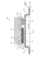
- FIG. 1 is a cross-sectional view schematically showing a semiconductor device 100 according to the present embodiment.
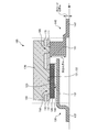
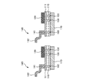
- 2 and 3 are cross-sectional views schematically showing another example of the semiconductor device 100 according to the present embodiment.
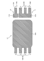
- FIG. 4 is a plan view schematically showing the semiconductor device 100 according to the present embodiment.
- FIG. 7 is a cross-sectional view schematically showing a conventional semiconductor device 1000.
- FIG. 8 is a plan view schematically showing a conventional semiconductor device 1000.
- FIG. FIG. 9 is a plan view schematically showing the arrangement of electrodes of the conventional semiconductor device 1000. Referring to FIG.
- the conventional semiconductor device 1000 includes a resin substrate 1100 having an adhesive layer 1110 on one surface and a semiconductor element 1200 fixed to the resin substrate 1100 via the adhesive layer 1110. , The shim 1400 connected to the semiconductor device 1200 via the via 1300, the first lead 1500 connected to the semiconductor device 1200, and the second lead 1600 or the third lead connected to the shim 1400 via the solder 2000 And a sealing resin 1800 for molding the semiconductor device 1000.
- the semiconductor chip 12000 is fixed to the island 1510 via the fixing material 2000, a gap is generated between the lead 1610 and the adhesive layer 1110.
- the shim 1400 is a hexahedral conductive material that fills this gap.
- the first lead 1500 is connected to the drain electrode on the back surface of the semiconductor element 1200, and the second lead 1600 is connected to the source electrode of the semiconductor element 1200,
- the third lead 1700 is connected to the gate electrode of the semiconductor device 1200.
- the first lead 1500 is a first adhesive portion 1510 (also referred to as an island) joined with the back surface of the semiconductor element 1200 by the solder 2000, and a first lead extending from the sealing resin 1800. And an exposed portion 1520.
- the second lead 1600 has a second bonding portion 1610 joined to the shim 1400 by the solder 2000, and a second exposed portion 1620 extending from the sealing resin 1800.
- the third lead 1700 has a third bonding portion 1710 joined to the shim 1400 by the solder 2000, and a third exposed portion 1720 extending from the sealing resin 1800.
- the shim 1400 is fixed to the adhesive layer 1110 by, for example, a mounting device at the same timing as the mounting of the semiconductor element 1200.
- the shim is then connected to the common electrode 1900 via the via 1300.
- the second lead 1600 and the third lead 1700 (not shown) are fixed to the shim 1400 via a bonding material such as solder 2000.
- the problem here is bonding using solder 2000, which may cause cracking or the like.
- the portion joined by the solder 2000 has high resistance, the characteristics of the semiconductor device 1000 may be reduced.
- the semiconductor device 1000 in order to avoid such a problem, it is required to reduce the number of bonding portions of the solder 2000 as much as possible.
- the semiconductor device 1000 may be a bipolar transistor or an IGBT instead of a MOSFET.
- power TRs such as SiC or GaN.
- such a semiconductor device 1000 generally adopts a metal thin wire by a bonding method, and often connects the semiconductor element 1200 and a lead.
- the source electrode of the semiconductor device 1200 and the second lead 1600, and further, the gate electrode and the third lead 1700 are connected by a thin metal wire. Therefore, there is a possibility that an inductance component may be generated due to the resistance of the metal thin wire. Furthermore, there is a possibility that element degradation and the like may occur due to bonding shock.
- the shim 1400 corresponding to the thickness of the semiconductor element 1200.
- One surface of the shim 1400 is connected to the via 1300 via the adhesive layer 1110, and the other surface of the shim 1400 is joined to the second lead 11600 and the third lead 1700 via the solder 2000.
- the other surface of the shim 1400 is connected by the solder, there is a problem that the resistance due to the solder is generated.
- two steps of the process of mounting the shim 1400 and the process of fixing the first lead 1600 and the third lead 1700 are required.
- the resin sheet 1100 is placed on a metal lead frame, a problem in which a contact failure occurs is also found due to the difference in thermal expansion coefficient.
- the semiconductor device 100 includes a resin substrate 110, a semiconductor element 120, a first connection member 130, a second connection member 140, and a third connection member 142A.
- the two common electrodes 170 and 170A are integrally formed by plating including the vias 150, 160, 150A, and 160A.
- the common electrodes 170 and 170A described above are formed on the surface of the resin substrate 110 opposite to the adhesive layer 111.
- the semiconductor element 120 is connected to the common electrodes 170 and 170A through the vias 150, 160, 150A and 160A.
- the common electrodes 170 and 170A are described in the conventional description, they replace the metal thin wires.
- the common electrode 170 source wiring
- the common electrode 170A gate electrode
- the common electrode has a thickness so as to suppress the resistance component and the inductance component.
- the common electrodes 170 and 170A may be formed by plating, or may be formed by plating, and a conductive plate or the like may be bonded thereon.
- the plating thickness is, for example, as thick as about 200 ⁇ m, and in the latter case, the plating thickness is about 50 ⁇ m.
- the conductive plate is made of Cu and has a thickness of about 100 ⁇ m to 1000 ⁇ m. Here, it is formed by the former Cu plating process.
- the resin substrate 110 is a flexible substrate and is a stable non-flowable thin layer or film substrate.
- the resin substrate 110 is made of a polyimide substrate, and Kapton (registered trademark), Ultem (registered trademark), polytetrafluoroethylene (PTFE), Upilex (registered trademark), polysulfone material (for example, , Udel (registered trademark), Radel (registered trademark), or liquid crystal polymer (LCP).
- the connection between the surface of the semiconductor device 100 and the common electrode 170, that is, the interface between the two, can relieve the stress generated here and maintain the electrical characteristics by this flexibility. .
- the polyimide resin employ
- the polyimide resin is a generic name of a polymer in which an imide resin is polymerized, and usually refers to an aromatic polyimide in which an aromatic compound is directly linked by an imide bond.
- the aromatic polyimide has a rigid and strong molecular structure because the aromatic and the aromatic have a conjugated structure via an imide bond.
- polyimide resins due to the strong intermolecular force of the imide bond, polyimide resins have good frequency characteristics and have the highest levels of thermal, mechanical and chemical properties among all polymers. Therefore, as in the present embodiment, it is suitable for a power transistor that can flow a large current and generate high heat, and is also useful for flexibility and stress relaxation.
- the semiconductor element 120 is provided on the resin substrate 110 face down, and is, for example, a MOSFET (field effect transistor), an IGBT (insulated gate bipolar transistor), a BIP (bipolar transistor) or the like.
- MOSFET field effect transistor
- IGBT insulated gate bipolar transistor
- BIP bipolar transistor
- Si-based, GaAs-based, SiC-based, GaN-based when a MOSFET is employed as the semiconductor element 120, a gate electrode and a source electrode are provided on the upper surface, and a drain electrode is provided on the lower surface.
- BJT bipolar junction transistor
- a base electrode and an emitter electrode are provided on the upper surface, and a collector electrode is provided on the lower surface.
- control electrode The gate electrode and the base electrode are referred to as "control electrode”
- current inflow electrode or “current outflow electrode”
- current outflow electrode or It may be called “current inflow electrode”.
- the semiconductor element 120 includes a source electrode (first electrode 121) connected to the first via 150, a gate electrode (control electrode 122) connected to the third via 150A, and the first via
- the common electrode 170 integrally formed with the electrode 150 is connected to the second connection member 140 integrated with the shim via the second via 160.
- the gate electrode 122 is connected to one end of a common electrode 170A integrally formed with the third via 150A, and integrated with the same material as the shim via a fourth via 160A located at the other end of the common electrode 170A.
- the third connecting member 142A is employed as the semiconductor element 120.
- the drain electrode (second electrode 123) and the island 131 are electrically connected and fixed to the back surface and the drain side of the semiconductor element 120.
- the island 131 is led to the side of the integrally formed first connection member 130, is bent, and extends as a first lead 132.
- the first electrode 121 is, for example, a source electrode
- the control electrode 122 is, for example, a gate electrode
- the second electrode 123 is, for example, a drain electrode (current outflow or inflow electrode).
- the thickness of the semiconductor element 120 is preferably 40 ⁇ m to 400 ⁇ m.
- the first connection member 130 and the second connection member 140 which are formed on the surface of the resin substrate 110 instead of the fine metal wires and integrally formed with the island 131 made of Cu through the common electrodes 170 and 170A.
- the semiconductor device 100 can cope with a large current because the current flows in and out through and. Furthermore, since the common electrode 170 covers the chip and has a thickness, larger current can be accommodated.
- the second connection member 140 and the third connection member 142A are obtained by integrating a portion corresponding to a conventional shim and a Cu lead. Such an integral structure can be processed by mechanical processing such as punching or etching. Furthermore, since the shim sides of the second connection member 140 and the third connection member 142A have a connection structure by plating in which the common electrodes 170 and 170A and the via are integrated, no solder is adopted at all. Therefore, the resistance component and the inductance component can be greatly reduced.
- the first connection member 130 is integrally formed with the island 131 fixed to the surface of the semiconductor element 120 opposite to the resin substrate 110, and extends in one direction parallel to one surface of the resin substrate 110. And a first lead 132.
- the first connection member 130 may be processed by bending between the island 131 and the first lead 132 in a gull wing shape (L-shape).
- the island 131 and the first lead 132 are formed of a conductive material such as copper or aluminum.
- the island 131 is formed, for example, by etching or punching a conductive plate. Further, by having a structure in which the back surface of the island 131 and / or the front side of the common electrode 170 is exposed from the sealing resin 180, the heat dissipation can be improved.
- the second connection member 140 is a member electrically connected to the semiconductor element 120 through the second via 160, the common electrode 170, and the first via 150.
- the first connection member 130 has a conductive portion 141 corresponding to a shim, and a second lead 142 integrally formed with the conductive portion 141 and extending from the sealing resin 180.
- the conductive portion 141 and the second lead 142 are manufactured, for example, by punching and are formed of a conductive material such as copper or aluminum.
- the conductive portion 141 and the second lead 142 are integrally manufactured without using solder.
- the conductive portion 141A corresponding to a shim and the third lead 142A are integrally formed.
- the two conductive parts 141, 141A corresponding to the shims have a predetermined thickness.
- the thickness is the sum of the thickness of the semiconductor element 120, the thickness of the adhesive layer 111 (here, solder or conductive paste) and the thickness of the island 131.
- the back surface of the island 131 is flush with the back surface of the conductive portion 141 and 141 A, and the first lead extending from the island 131 Since the back surface of 132, the back surface of the second lead 142 extending from the conductive portion, and the back surface of the third lead 142A are flush with each other, they can be easily brought into contact with the lower mold, so that the manufacturing reliability is achieved. Improve.
- each of the conductive parts 141 and 141A may be formed thicker than the total thickness of the semiconductor element 120 and the island 131.
- the heat dissipation of the conductive portions 141 and 141A is further improved, and the thermal characteristics of the semiconductor device 100 are further improved.
- the conductive portions 141 and 141A have a thickness such that the second lead 142 and the third lead 142A do not contact the adhesive layer 111 in the manufacturing process, and the second lead 142 and the The three leads 142A may be formed to have substantially the same thickness.
- the conductive portion is formed to have such a thickness that the relationship of the thickness of the conductive portions 141 and 141A> the thickness of the second lead 142 and the thickness of the third lead 142A holds.
- the second lead 142 and the third lead 142A are bent in a gull-wing shape, and for example, the contact portion extended from the sealing resin 180 is formed to be flush with the first lead 132.
- the first via 150 to the fourth via 160A are processed by irradiating the resin substrate 110 with a laser. However, it may be formed by plasma etching or mechanical drilling process.
- the first via holes 151 to the fourth via holes 161A are filled with, for example, a conductive material by plating to form vias, and are integrally formed with the common electrode.
- the material is generally based on copper, but may be based on Al or an alloy containing Cu or Al.
- the sealing resin 180 is a member that covers and integrally supports the first connection member 130 to the third connection member 142A that are integrated with the semiconductor element 120 and the island 131.
- the sealing resin 180 may be, for example, a thermosetting resin or a thermoplastic resin.
- the sealing method can be transfer molding, injection molding, potting method, vacuum printing, and the like.
- the sealing resin 180 is not essential and may not be adopted. Also, as described above, when the sealing resin is not adopted, the resin substrate 110 and the first to third leads 132, 142 and 142A, the resin substrate 110 and the island 131, and the periphery of the semiconductor element 120 are like underfills. A resin may be applied.
- FIG. 5A In order to give stability to the resin substrate 110, a ring-shaped frame 200 is disposed around the front side of the resin substrate 110 (which will be the back side in FIG. 1).
- the adhesive layer 111 is formed on one surface of the resin substrate 110.
- the adhesive layer 111 may be formed on the entire surface of the resin substrate 110 before the frame 200 is fixed, and then the frame 200 may be fixed.
- an adhesive layer is provided, and a resin substrate 110 provided with a frame around the periphery is prepared.
- one or more semiconductor elements 120 and the second connection members 140 are fixed to the resin substrate 110 via the adhesive layer 111.
- the semiconductor element 120 is fixed to the resin substrate 110 by curing the adhesive layer 111 in a state in which the semiconductor element 120 is disposed on the adhesive layer 111 in a semi-cured state.
- the shim 1400 is fixed to the adhesive layer 111 instead of the second connection member 140, and then the second lead 1600 is fixed to the shim 1400 via the solder 2000.
- the working process can be reduced by using the second connection member 140 in which the shim 1400 and the second lead 1600 are integrally formed without using the solder 2000.
- the first lead 142 may be formed to extend horizontally from the conductive portion 141.
- two units are illustrated as semiconductor devices, in actuality, two units are formed of a collective substrate in which the units are vertically and horizontally arranged in a matrix in plan view, and mounters are mounted on the respective units.
- a plurality of via holes 151 and 161 are formed in the resin substrate 110 and the adhesive layer 111.
- the via holes 151 and 161 are formed, for example, by a laser.
- the via holes 151 and 161 are filled with a conductive material by plating.
- a conductive material is formed on the back side of the resin substrate 110 by plating. Therefore, the vias 150 and 160 and the common electrode 170 are integrally formed by Cu plating.
- the pattern may be formed by patterning the resin substrate 110 in the desired shape after plating the entire surface, or forming the plating resist and partially plating the common electrodes 170 and 170A.
- the common electrodes 170 and 170A may be formed thin and a Cu plate may be bonded using a conductive adhesive. In this way, the plating time can be shortened.
- the present invention is not limited thereto.
- the semiconductor element 120 and the second connection member 140 may be fixed to the resin substrate 110 after the via holes 151 and 161 are formed.
- the resin substrate 110 is removed from the frame 200.
- the resin substrate 110 is singulated into a predetermined size.
- the first connection member 130 is attached to the drain electrode side of the singulated semiconductor device 100 through solder 190 or Ag paste.
- the semiconductor device 100 is sealed by sealing with a sealing resin 180.
- one semiconductor element 120 is mounted on a die pad, but a plurality of semiconductor elements 120 may be mounted or passive elements may be mounted.
- the conductive portion 141 (second conductive portion) in which three second leads 142 are integrated, and the conductive portion 141A (first conductive portion) on the die pad side of the third lead 142A It is a part caused by
- the conductive portions 141 and 141A have a thickness and a volume.
- distortion occurs due to the difference in thermal expansion coefficient ⁇ between the lead frame of these metals, the resin substrate 110, the semiconductor element 120, and the adhesive 111.
- the volume is large, so the amount of expansion and contraction is also large.
- a load is applied to the third via 150A (first contact hole) and the gate wiring 170A, which may cause a defect.
- the gate electrode 122 and the gate wiring 170A which are control electrodes are formed to be small in size.
- a control electrode (gate electrode 122) is provided on the semiconductor element 120 side, and one end of the gate wiring 170A is a through hole (first contact hole) which is the third via 150A of the resin substrate 110. Contact with the gate electrode 122 of the semiconductor element 120). That is, this end is connected to the gate electrode 122 and extends toward the fourth via 160A as the gate wiring 170A.
- one end of the gate wiring 170A may be described as the gate electrode 122.
- a rectangular electrode indicated by a broken line provided on the semiconductor element 120 side is the source electrode, and the common electrode 170 (source wiring) provided on the resin substrate 110, particularly the semiconductor element The portion located above 120 may be described as the source electrode 121.
- the size of the control electrode which is the size of the gate electrode 122 here, is smaller than the size of the source electrode 121.
- the gate wiring 170 ⁇ / b> A integrated with the gate electrode 122 is narrower than the width of the source wiring 170.
- the hole diameter of the third via 150A (first contact hole) is formed small for the reasons described above, and the number thereof is small, and generally one.
- the number of first vias 150 (second contact holes) of the source electrode 121 is one, but a plurality of first vias 150 (second contact holes) may be vertically and horizontally arranged.
- strain is generated in a space located between one end of the gate wiring 170A (the gate electrode 122 on the resin substrate 110) and the source wiring 170.
- An absorber in particular a slit Gs (opening) was provided.
- the slit Gs is provided along the corner of one end of the gate wiring 170A. That is, the slit Gs is provided in the exposed portion of the resin substrate 110 between the gate electrode 122 and the source electrode 121, and is provided in a portion which is L-shaped by the vertical space and the horizontal space. A combination of or a L-shaped slit may be provided.
- the slit Gs is an opening that penetrates the resin substrate 110 and the adhesive layer 111.
- This slit Gs may be formed at the time of via formation, or may be formed after the semiconductor element 120 is fixed.
- the processing method of the slit Gs mainly uses laser processing, and the resin substrate 110 and the lower adhesive layer 111 are removed.
- the strain absorbing portion may be cut with a cutter instead of the laser. The cut formed by the cutter penetrates the resin substrate 110 but does not form an opening. That is, the cut surfaces facing each other in the inside of the cut are in contact with each other.
- the common electrodes 170 and 170A can be formed thick by plating, the resistance value can be significantly reduced because the thickness and the area are larger than that of the thin metal wire.
- the semiconductor element 120 can employ a power transistor with large current and high heat generation.
- first to third connecting members 130, 140 and 142A which are leads integrated with the conventionally used shims are used, and the connecting portion by the solder is eliminated, the resistance of the portion can be reduced.
- the thickness obtained by adding up the thickness of the semiconductor element 120, the thickness of the adhesive layer 111, and the thickness of the island 131 and the thickness of the conductive portion 141 of the second connection member 140 are formed to have the same thickness. Therefore, since the back surface of the island 131 and the back surface of the conductive portion 141 are flush with each other (FIG. 1), it can be disposed flatly in a mold or the like.
- the portion corresponding to the shim since the portion corresponding to the shim does not only omit the solder but also has a function as a heat sink, it can cope with a large current and can cope with a transient thermal destruction.
- the second connection member 140 corresponding to the source electrode is provided with a portion corresponding to a shim having a thickness in a portion corresponding to reference numeral 1900 shown in FIG. 9, a large amount of heat can be stored. It has a function, and its effect is great as a thermal destruction prevention.
- Reference Signs List 100 semiconductor device 110 resin substrate 111 adhesive layer 120 semiconductor element 121 first electrode 122 control electrode 123 second electrode 130 first connection member 131 island 132 first lead 140 second connection member 141 conductive portion 142 second lead 150 first via 160 second via 170 common electrode 180 sealing resin
Landscapes
- Structures Or Materials For Encapsulating Or Coating Semiconductor Devices Or Solid State Devices (AREA)
Abstract
【課題】 一方の面に接着層を有する、可撓性の樹脂基板と、前記接着層を介して、前記樹脂基板の一方の面に、フェイスダウンで設けられた半導体素子と、前記半導体素子における前記樹脂基板と反対側の面に固着されるアイランドと、前記アイランドと一体的に形成され、前記樹脂基板の一方の面と平行な一方向に延出する第1リードと、を有する第1接続部材と、前記樹脂基板の一方の面において前記半導体素子と隣り合って設けられ、前記樹脂基板に固着される導電部と、前記導電部と一体的に形成され、前記一方向とは異なる他方向に延出する第2リードと、を有する第2接続部材と、前記半導体素子の表面電極が露出するように前記樹脂基板に設けられる第1コンタクト孔に、導電材料を導入して形成される第1ビアと、前記導電部が露出するように前記樹脂基板に設けられる第2コンタクト孔に、導電材料を導入して形成される第2ビアと、前記樹脂基板の他方の面に設けられ、前記第1ビアと前記第2ビアとを接続する共通電極と、を備える。
Description
本発明は、半導体装置、半導体装置の製造方法に関する。
例えば、ワイヤボンドを有するPOL構造体がある。
特許文献1に記載されているPOL構造体においては、ワイヤボンディングに比べて、放熱性の低下や寄生インダクタンスの増大を抑制することができる。しかし、該POL構造体では、半導体素子の接合に半田を用いているため、抵抗値の増大や半田亀裂などによる信頼性の低下を引き起こす虞があった。
一方、POL技術を用いた半導体デバイスでは、半導体素子とリードを接続する場合、半導体素子の厚み分のギャップが発生し、リードとの接続にはシム(ギャップを埋める金属体)が必要な場合がある。このシムとリードとの接合には半田などのロウ材を用いているため、上記と同様のロウ材の抵抗上昇の問題に加えて、半田接続の工程を要することから製作効率が低下する虞があった。
本発明の1つの側面に係る半導体装置は、一方の面に接着層を有する、可撓性の樹脂基板と、前記接着層を介して、前記樹脂基板の一方の面に、フェイスダウンで設けられた半導体素子と、前記半導体素子における前記樹脂基板と反対側の面に固着されるアイランドと、前記アイランドと一体的に形成され、前記樹脂基板の一方の面と平行な一方向に延出する第1リードと、を有する第1接続部材と、前記樹脂基板の一方の面において前記半導体素子と隣り合って設けられ、前記樹脂基板に固着される導電部と、前記導電部と一体的に形成され、前記一方向とは異なる他方向に延出する第2リードと、を有する第2接続部材と、前記半導体素子の表面電極が露出するように前記樹脂基板に設けられる第1コンタクト孔に、導電材料を導入して形成される第1ビアと、前記導電部が露出するように前記樹脂基板に設けられる第2コンタクト孔に、導電材料を導入して形成される第2ビアと、前記樹脂基板の他方の面に設けられ、前記第1ビアと前記第2ビアとを接続する共通電極と、を備える。
その他、本願が開示する課題、及びその解決方法は、発明を実施するための形態の欄の記載、及び図面の記載等により明らかにされる。
本発明によれば、シムとフレームとを接合するための半田接続の箇所を削減できるため、半導体装置の特性を向上させることができるとともに、製作効率の向上が図れる。
以下、適宜図面を参照し、本発明の実施形態に係る電源モジュールについて説明する。なお、図面において共通の又は類似する構成要素には同一又は類似の参照符号が付されている。
===半導体装置100の構成===
図1、図2、図3、図4、図7~図9を参照しつつ、本実施形態における半導体装置100について以下のとおり説明する。図1は、本実施形態に係る半導体装置100を概略的に示す断面図である。図2、図3は、本実施形態に係る半導体装置100の他の一例を概略的に示す断面図である。図4は、本実施形態に係る半導体装置100を概略的に示す平面図である。図7は、従来の半導体装置1000を概略的に示す断面図である。図8は、従来の半導体装置1000を概略的に示す平面図である。図9は、従来の半導体装置1000の電極の配置を概略的に示す平面図である。
図1、図2、図3、図4、図7~図9を参照しつつ、本実施形態における半導体装置100について以下のとおり説明する。図1は、本実施形態に係る半導体装置100を概略的に示す断面図である。図2、図3は、本実施形態に係る半導体装置100の他の一例を概略的に示す断面図である。図4は、本実施形態に係る半導体装置100を概略的に示す平面図である。図7は、従来の半導体装置1000を概略的に示す断面図である。図8は、従来の半導体装置1000を概略的に示す平面図である。図9は、従来の半導体装置1000の電極の配置を概略的に示す平面図である。
従来の半導体装置1000は、例えば、図7、図8に示すように、一方の面に接着層1110を有する樹脂基板1100と、該接着層1110を介して樹脂基板1100に固着される半導体素子1200と、半導体素子1200とビア1300を介して接続されるシム1400と、半導体素子1200と接続される第1リード1500と、半田2000を介してシム1400と接続される第2リード1600または第3リード1700と、半導体装置1000をモールドする封止樹脂1800と、を有する。尚、アイランド1510に固着材2000を介して半導体チップ12000を固着されることから、リード1610と接着層1110の間にギャップが発生する。シム1400は、このギャップを埋める6面体から成る導電材である。
図9に示すように、例えば、半導体装置1000がMOSFETである場合、第1リード1500が半導体素子1200の裏面のドレイン電極に接続され、第2リード1600が半導体素子1200のソース電極に接続され、第3リード1700が半導体素子1200のゲート電極に接続される。図7、図9に示すように、第1リード1500は、半導体素子1200の裏面と半田2000で接合される第1接着部1510(アイランドとも言う)と、封止樹脂1800から延出する第1露出部1520と、を有する。また、第2リード1600は、シム1400と半田2000で接合される第2接着部1610と、封止樹脂1800から延出する第2露出部1620と、を有する。また、第3リード1700は、シム1400と半田2000で接合される第3接着部1710と、封止樹脂1800から延出する第3露出部1720と、を有する。
このような半導体装置1000の製造過程において、シム1400は、半導体素子1200の実装と同じタイミングで、例えばマウンティング装置で接着層1110に固着される。そして、シムは、共通電極1900にビア1300を介して接続される。そして、図7に示すように、第2リード1600、第3リード1700(不図示)は、半田2000などの接合材を介して該シム1400に固着される。ここで問題となるのは、半田2000を用いた接合で、亀裂などを生じる可能性がある。また、半田2000で接合されている部分は、高い抵抗を有するため、半導体装置1000の特性を低減させる虞がある。半導体装置1000においては、このよう問題を回避するために、極力、半田2000の接合部分を少なくすることが求められている。なお、半導体装置1000がMOSFETではなく、バイポーラトランジスタまたはIGBTでも良い。また、材料系で言うと、SiCまたはGaNなどのパワーTRでも同様の問題を生じる虞がある。
さらに、このような半導体装置1000は、一般に、ボンディング法による金属細線を採用し、半導体素子1200とリードを接続する場合が多い。この場合、半導体素子1200のソース電極と第2リード1600、更には、ゲート電極と第3リード1700を金属細線でつなぐ。そのため、その金属細線による抵抗分、インダクタンス成分が発生する虞があった。更に、ボンディング衝撃による素子劣化等を生じる虞があった。
更に、パワーオーバーレイ技術を用いた半導体装置1000では、上述したように、半導体素子1200の厚みに応じたシム1400を用いる必要がある。シム1400の一方の面は接着層1110を介してビア1300と接続され、シム1400の他方の面は半田2000を介して第2リード11600、第3リード1700と接合されている。このように、シム1400の他方の面は半田で接続されるため、半田による抵抗分が発生するという問題があった。また、半導体素子1200の実装と同時に、シム1400を載せる工程と、その後、第1リード1600、第3リード1700を固定させる工程の、二つの工程を要していた。また、金属のリードフレームの上に樹脂シート1100がのるため、熱膨張係数の違いで、コンタクト不良が発生する課題も見つかった。
以下、本発明の実施の形態を説明する。本実施形態に係る半導体装置100は、図1乃至図4に示すように、樹脂基板110と、半導体素子120と、第1接続部材130と、第2接続部材140と、第3接続部材142Aと、ソース側の第1ビア150と、シム側の第2ビア160と、ゲート側の第3ビア150Aとシム側の第4ビア160Aと、ソース側の共通電極170と、ゲート側の共通電極170Aと、封止樹脂180と、を含んで構成されている。尚、二つの共通電極170,170Aは、ビア150,160,150A,160Aも含めメッキにより一体で形成されている。
また、半導体装置100は、樹脂基板110における接着層111とは反対側の面に、前述した共通電極170、170Aが形成される。半導体素子120はビア150、160、150A、160Aを介して該共通電極170、170Aに接続される。この共通電極170、170Aは、従来の説明で述べたが、金属細線の代わりとなる。具体的には、図4で示すように、共通電極170(ソース配線)は半導体素子120を覆う大きな面積を有し、共通電極170A(ゲート電極)は、金属細線よりも幅の大きい配線である。しかも、共通電極は、抵抗分やインダクタンス成分を抑制するように、厚みを有する。また、この共通電極170、170Aは、メッキで形成されるもの、またはメッキで形成し、その上に導電板などを貼り合わせて形成されても良い。前者のメッキで完結するものは、メッキ厚が例えば厚くて200μm前後、後者は、メッキ厚が50μm前後である。そして、導電板は、Cuからなり、100μm~1000μm程度である。尚、ここでは、前者のCuメッキ処理により形成されている。
樹脂基板110は、可撓性基板で、安定した非流動性の薄層体またはフィルム状の基板である。樹脂基板110は、ポリイミド基板からなり、カプトン(Kapton)(登録商標)、ウルテム(Ultem)(登録商標)、ポリテトラフルオロエチレン(PTFE)、ユーピレックス(Upilex)(登録商標)、ポリスルフォン材料(例えば、ユーデル(Udel)(登録商標)、レイデル(Radel)(登録商標))、または液晶ポリマー(LCP)などから選択される。
樹脂基板110を用いることにより、半導体装置100表面と共通電極170との接続部、つまり両者の界面は、この可撓性により、ここに生じる応力を緩和し、電気的特性を維持することができる。
なお、本実施形態で採用されたポリイミド樹脂について説明する。このポリイミド樹脂は、イミド樹脂が重合された高分子の総称であり、通常は芳香族化合物が直接イミド結合で連結された芳香族ポリイミドをいう。芳香族ポリイミドは、芳香族と芳香族がイミド結合を介して共役構造を有するため、剛直で強固な分子構造を有する。さらに、イミド結合が強い分子間力を有するため、ポリイミド樹脂は、周波数特性がよく、すべての高分子中で最高レベルの高い熱的、機械的、化学的性質を有する。そのため、本実施例の様に、大電流を流せ、高発熱を発生するパワートランジスタには好適で、しかも可撓性から応力緩和にも有用である。
半導体素子120は、樹脂基板110にフェイスダウンで設けられ、例えば、MOSFET(電界効果トランジスタ)、IGBT(絶縁ゲートバイポーラトランジスタ)、BIP(バイポーラトランジスタ)などである。材料で述べれば、Si系、GaAs系、SiC系、GaN系である。例えば、半導体素子120にMOSFETが採用される場合は、上面にゲート電極およびソース電極が設けられ、下面にドレイン電極が設けられる。また、例えば、半導体素子120にBJT(バイポーラ接合トランジスタ)が採用される場合は、上面にベース電極およびエミッタ電極が設けられ、下面にコレクタ電極が設けられる。尚、ゲート電極やベース電極を「制御電極」と呼び、ソース電極、コレクタ電極を「電流流入電極」(または「電流流出電極」)と呼び、ドレイン電極、エミッタ電極を「電流流出電極」(または「電流流入電極」)と呼ぶことがある。
以下の説明においては、半導体素子120としてMOSFETを採用するものとする。半導体素子120は、図1に示すように、第1ビア150に接続されるソース電極(第1電極121)、および第3ビア150Aに接続されるゲート電極(制御電極122)と、第1ビア150と一体で形成された共通電極170は、第2ビア160を介して、シムと一体の第2接続部材140に接続される。更に、ゲート電極122は、第3ビア150Aと一体で形成された共通電極170Aの一端に接続され、この共通電極170Aの他端に位置する第4ビア160Aを介して、シムと同一材料で一体となった第3接続部材142Aと接続される。
更には、半導体素子120の裏面、ドレイン側は、ドレイン電極(第2電極123)とアイランド131が電気的に接続されて固着されている。このアイランド131は、一体で形成された第1接続部材130側へと導出され、折り曲げられて第1リード132として延在している。なお、上述したように、第1電極121は例えばソース電極であり、制御電極122は例えばゲート電極であり、第2電極123は例えばドレイン電極(電流の流出電極または流入電極)である。なお、半導体素子120の厚みは、40μm~400μmであることが好ましい。
以上の様に、金属細線の代わりに樹脂基板110の表面に形成され、共通電極170,170Aを通じて、Cuからなるアイランド131と一体に形成される第1接続部材130と、第2接続部材140と、を介して電流が出入りするため、半導体装置100は大電流に対応できる。さらに、共通電極170がチップを覆い、厚みを有するため、より大きな電流に対応できる。
更には、第2接続部材140、第3接続部材142Aは、従来のシムに相当する部分とCuのリードが一体となったものである。尚、このような一体構造は、パンチング等の機械的加工やエッチングで加工ができる。更に、第2接続部材140、第3接続部材142Aのシム側は、共通電極170、170Aとビアが一体の、メッキによる接続構造であるため、いっさい半田を採用しない構造となる。よって抵抗分、インダクタンス成分を大きく減らせる。
第1接続部材130は、半導体素子120における樹脂基板110と反対側の面に固着されるアイランド131と、それと一体的に形成され、樹脂基板110の一方の面と平行な一方向に延出する第1リード132と、を有する。第1接続部材130は、例えば、アイランド131と第1リード132との間をガルウイング状(L字状)に折り曲げ加工されていても良い。アイランド131および第1リード132は、銅やアルミニウムなどの導電材料で形成されている。アイランド131は、例えば導電板をエッチング加工または打ち抜き加工することにより形成される。また、アイランド131の裏面または/および共通電極170の表側が封止樹脂180から露出する構造を有することで、放熱性の向上が図れる。
第2接続部材140は、第2ビア160、共通電極170および第1ビア150を介して半導体素子120に電気的に接続される部材である。第1接続部材130は、シムに相当する導電部141と、導電部141と一体的に形成され、封止樹脂180から延出する第2リード142と、を有する。導電部141および第2リード142は、例えば、打ち抜き加工で製作され、銅やアルミニウムなどの導電材料で形成されている。このように、第2接続部材140は、半田を用いずに、導電部141と第2リード142とが一体的に製作される。また、同様に、第3接続部材142Aもシムに相当する導電部141Aと第3リード142Aとが一体で形成されている。これにより、半田による気泡破裂やクラックを回避することができ、また、半田が有する抵抗分を削減することができるため、半導体装置100の特性が向上する。
シムに相当する二つの導電部141、141Aは、所定の厚みを有する。具体的には、例えば、半導体素子120の厚み、接着層111(ここでは半田や導電ペースト)の厚みおよびアイランド131厚みを合算した厚みである。これにより、導電部に発生する熱は、ヒートシンクとして蓄熱できると同時に、放熱性を確保できる。
また、図1では、トランスファーモールド、真空印刷などの樹脂封止した状態において、アイランド131の裏面と導電部141、141Aの裏面とが面一であり、また、アイランド131から延出する第1リード132の裏面と、導電部から延出する第2リード142の裏面および第3リード142Aの裏面とが面一であるため、簡単に下金型に当接させることができるため、製作の信頼性が向上する。
また、例えば、図2に示すように、それぞれの導電部141、141Aは、半導体素子120およびアイランド131を合算した厚みよりも厚く形成されていてもよい。これにより、導電部141、141Aの放熱性がより向上するため、半導体装置100の熱特性がより向上する。また、例えば、図3に示すように、導電部141、141Aは、製作工程において第2リード142、第3リード142Aが接着層111に接触しない程度の厚みであって、第2リード142、第3リード142Aと略同一の厚みで形成されていてもよい。リードを樹脂基板110に取り付ける際、一般には曲げ加工する前、隙間があるため第2リード142、第3リード142Aが接着層111に付かず、作業性に優れるからである。つまり、導電部は、導電部141、141Aの厚み>第2リード142、第3リード142Aの厚み、の関係が成り立つ厚みを有するように形成される。
第2リード142、第3リード142Aは、ガルウイング状に折り曲げ加工され、例えば封止樹脂180から延出した当接部分が第1リード132と面一になるように形成されている。
第1ビア150乃至第4ビア160Aは、樹脂基板110に、レーザを照射して加工される。しかし、プラズマエッチングまたは機械的な穴あけプロセスによって形成しても良い。またこの第1ビア孔151乃至第4ビア孔161A(図5Dを参照)は、例えば導電材をメッキ処理して充填されてビアとなり、共通電極と一体で形成される。材料は、一般には銅を主材料としたものであるが、Alを主材料としたもの、またはCuまたはAlを含んだ合金であってもよい。
封止樹脂180は、半導体素子120、アイランド131と一体の第1接続部材130乃至第3接続部材142Aを被覆して一体的に支持する部材である。封止樹脂180は、例えば、熱硬化性の樹脂、熱可塑性の樹脂でも良い。封止法は、トランスファーモールド、インジェクションモールド、ポッティング法または真空印刷などが可能である。尚、封止樹脂180は、必須ではなく、採用しなくも良い。また、この様に、封止樹脂が採用されない場合、樹脂基板110と第1乃至第3リード132,142,142A、樹脂基板110とアイランド131、そして半導体素子120の周囲には、アンダーフィルの如き樹脂が塗布されても良い。
===半導体装置100の製造工程===
図5A~図5I、図6A~図6Bを参照しつつ、本実施形態における半導体装置100の製造方法について以下のとおり説明する。
図5A~図5I、図6A~図6Bを参照しつつ、本実施形態における半導体装置100の製造方法について以下のとおり説明する。
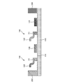
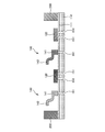
まず、図5Aから説明する。樹脂基板110に安定性を与えるため、樹脂基板110表側(尚、図1では裏側となる)の周囲にリング状のフレーム200を配置する。次に、図5Bに示すように、樹脂基板110がフレーム200に固着された状態において、樹脂基板110の一方の面に接着層111が形成される。尚、フレーム200を固着する前に、樹脂基板110全面に接着層111を形成し、その後でフレーム200を固定しても良い。ここで、接着層が設けられ、周囲に枠が設けられた樹脂基板110が用意される。
次に、図5Cに示すように、1つまたは複数の半導体素子120および第2接続部材140(141A、142A)が接着層111を介して樹脂基板110に固着される。このとき、半導体素子120を半硬化状態の接着層111に配置した状態において、接着層111を硬化させることで、半導体素子120を樹脂基板110に固着する。
従来は、この工程において、第2接続部材140の代わりにシム1400を接着層111に固着し、その後、シム1400に半田2000を介して第2リード1600を固着させていた。本実施形態においては、半田2000を用いずに、シム1400と第2リード1600が一体的に形成される第2接続部材140を用いることで、作業工程の減らすことができる。
なお、第2接続部材140は、湾曲加工されているが、導電部141から水平に延び出るように第1リード142が形成されていてもよい。また、半導体装置として2つのユニットが図示されているが、実際は平面視で縦横にマトリックス状に前記ユニットが並んだ集合基板からなり、夫々のユニットに、マウンターを採用して実装されている。
次に、図5Dに示すように、樹脂基板110および接着層111に複数のビア孔151,161を形成する。ビア孔151,161は、例えば、レーザによって形成される。
そして、図5Eに示すように、該ビア孔151,161には、メッキにより導電材が充填される。続けて、樹脂基板110の裏側に導電材がメッキで形成される。よってビア150,160と共通電極170は、Cuメッキにより一体で形成される。また、パターンの形成は、樹脂基板110に全面メッキの後に所望の形状にパターニングしても良いし、メッキレジストを形成して部分メッキで、共通電極170、170Aを形成しても良い。尚、この共通電極170、170Aを薄く形成し、導電性接着剤を用いて、Cu板を貼り合わせても良い。このようにすると、メッキ時間の短縮が可能である。
なお、図5C、図5Dにおいて、半導体素子120および第2接続部材140を固着した後に、ビア孔151,161を形成するように説明したが、これに限定されない。例えば、図6A、図6Bに示すように、ビア孔151,161を形成した後に、半導体素子120および第2接続部材140を樹脂基板110に固着させてもよい。
次に、図5F、図5G、図5Hに示すように、樹脂基板110は、フレーム200から外される。ここでは、その後で、樹脂基板110を所定の大きさに個片化している。個片化された半導体装置100のドレイン電極側には、半田190またはAgペーストなどを介して第1接続部材130が取り付けられる。そして、必要により、図5Iに示すように、封止樹脂180で樹脂封止して、半導体装置100が完成する。尚、本実施例は、ダイパッドに一つの半導体素子120を実装したが、複数の半導体素子120が実装されても良いし、受動素子が装着されても良い。
続いて、図4を参照しながら、更なる工夫に関して説明する。図4の平面図では、3本の第2リード142が一体となった導電部141(第2導電部)、第3リード142Aのダイパッド側の導電部141A(第1導電部)が、この工夫に起因する部分である。この導電部141,141Aは、厚みがあり、その体積もある。
半導体装置100において、これらの金属のリードフレーム、樹脂基板110、半導体素子120および接着剤111の熱膨張係数αの違いにより、歪が発生する。しかも、上述した導電部においては、その体積が大きいため、その伸び縮みの量も大きくなる。
半導体装置100において、これらの金属のリードフレーム、樹脂基板110、半導体素子120および接着剤111の熱膨張係数αの違いにより、歪が発生する。しかも、上述した導電部においては、その体積が大きいため、その伸び縮みの量も大きくなる。
さらに、図4の平面的なパターンにおいて、第3ビア150A(第1のコンタクト孔)やゲート配線170Aに負荷が加わり、不良が発生する虞がある。制御電極であるゲート電極122やゲート配線170Aは、サイズが小さく形成されている。ここで、半導体素子120側には制御電極(ゲート電極122)が設けられており、ゲート配線170Aの一方の端部は、樹脂基板110の第3ビア150Aである貫通孔(第1のコンタクト孔)を介して半導体素子120のゲート電極122とコンタクトしている。つまり、この端部は、ゲート電極122と接続され、ゲート配線170Aとして第4ビア160Aに向かって延在している。ここでは、ゲート配線170Aの一方の端部をゲート電極122として説明することもある。
また、ソース電極121も同様に、半導体素子120側に設けられている破線で示す矩形の電極がソース電極であり、樹脂基板110の上に設けられた共通電極170(ソース配線)、特に半導体素子120の上に位置する部分をソース電極121として説明することもある。
例えばFETであれば、ゲート電極には、電圧が印加されるだけで、電流は流れない。BIPトランジスタであれば、ベース電極に少ない電流しか流れない。そのため、制御電極のサイズ、ここではゲート電極122のサイズであるが、ソース電極121のサイズと比べて小さい。さらに、ゲート電極122と一体のゲート配線170Aは、ソース配線170の幅よりも狭い。さらに、第3ビア150A(第1のコンタクト孔)の孔径は上述の理由により、小さく形成され、その個数も少なく、一般的には一個である。
尚、図4に於いて、ソース電極121の第1ビア150(第2のコンタクト孔)は、一つであるが、縦横に複数並べられる場合もある。
この場合、半導体素子120に大電流が流れるため、半導体装置100全体の温度が上昇する。特に、アイランド131や導電部141、141Aは、体積が大きいため、その伸び縮みも大きくなることから、その分、樹脂基板110に応力が加わる。その結果、最も弱い部分、例えば第3ビア150A(第1のコンタクト孔)に負荷が加わり、第3ビア150A内のクラックや膜剥がれが発生したり、ゲート電極122と一体のゲート配線170Aにクラックや断線が生じる虞がある。
本実施形態では、この課題を解決するために、図4に示すようにゲート配線170Aの一方の端部(樹脂基板110上のゲート電極122)とソース配線170の間に位置するスペースに、ひずみ吸収部、特にスリットGs(開口部)を設けた。具体的には、図4において、スリットGsは、ゲート配線170Aの一方の端部の角に沿って設けられている。すなわち、スリットGsは、ゲート電極122とソース電極121の間の樹脂基板110の露出部分に設けられ、縦方向のスペースと横方向のスペースでL字になっている部分に設けられ、例えば直線状の組み合わせまたはL字状のスリットが設けられていればよい。スリットGsは、樹脂基板110および接着層111を貫通する開口である。このスリットGsを設けることにより、ゲート電極122やその周りに発生するひずみを吸収でき、前述した不良を抑制することができる。
このスリツトGsは、ビア形成時に形成しても良いし、半導体素子120を固着した後に形成しても良い。スリットGsの加工方法は、主にレーザによる加工が用いられ、樹脂基板110と下層の接着層111が取り除かれる。尚、このひずみ吸収部は、レーザの代わりにカッタで切り込んでも良い。カッタにより形成される切れ目は、樹脂基板110を貫通しているが開口を形成しない。すなわち、切れ目の内部において対向するカット面は、それぞれ当接している。
===まとめ===
以上説明したように、金属細線の代わりに、樹脂基板110に設けた共通電極170,170Aで半導体素子120と電気的に接続するため、抵抗成分、インダクタンス成分を減らせ、半導体装置100として特性を向上させることができる。
以上説明したように、金属細線の代わりに、樹脂基板110に設けた共通電極170,170Aで半導体素子120と電気的に接続するため、抵抗成分、インダクタンス成分を減らせ、半導体装置100として特性を向上させることができる。
また、共通電極170,170Aは、メッキで厚く形成可能であるため、金属細線と比べ、厚みや面積が広いため、抵抗値は大幅に低減できる。
また、樹脂基板110がポリイミド樹脂からなるため、半導体素子120は、大電流、高発熱のパワートランジスタを採用できる。
また、従来用いたシムと一体のリードである第1~第3接続部材130,140,142Aを採用し、半田による接続部をなくしたので、その部分の抵抗分も減らせるという特長を有する。
更には、半導体素子120の厚み、接着層111の厚みおよびアイランド131の厚みを合算した厚みと、第2接続部材140の導電部141の厚みと、が同じ厚みで形成される。そのため、アイランド131の裏面と導電部141の裏面とが面一になる(図1)ため、金型などに、平らに配置が可能となる。
また、シムに相当する部分は、半田が省略されるほか、ヒートシンクとしての機能も持たせられるため、大電流対応ができ、過渡的な熱破壊にも対応が可能である。特に、ソース電極に対応する第2接続部材140は、図9に示す符号1900に相当する部分に厚さのあるシムに相当する部分が設けられるため、熱量を大きく貯めることができ、ヒートシンクとしての機能を持たせられ、熱破壊防止としてもその効果は大である。
100 半導体装置
110 樹脂基板
111 接着層
120 半導体素子
121 第1電極
122 制御電極
123 第2電極
130 第1接続部材
131 アイランド
132 第1リード
140 第2接続部材
141 導電部
142 第2リード
150 第1ビア
160 第2ビア
170 共通電極
180 封止樹脂
110 樹脂基板
111 接着層
120 半導体素子
121 第1電極
122 制御電極
123 第2電極
130 第1接続部材
131 アイランド
132 第1リード
140 第2接続部材
141 導電部
142 第2リード
150 第1ビア
160 第2ビア
170 共通電極
180 封止樹脂
Claims (21)
- 一方の面に接着層を有する、可撓性の樹脂基板と、
前記接着層を介して前記樹脂基板の一方の面に設けられた半導体素子と、
前記半導体素子における前記樹脂基板と反対側の面に固着されるアイランドと、前記アイランドと一体的に形成され、前記樹脂基板の一方の面と平行な一方向に延出する第1リードと、を有する第1接続部材と、
前記樹脂基板の一方の面において前記半導体素子と隣り合って設けられ、前記樹脂基板に固着される導電部と、前記導電部と一体的に形成され、前記一方向とは異なる他方向に延出する第2リードと、を有する第2接続部材と、
前記半導体素子の表面電極が露出するように前記樹脂基板に設けられる第1コンタクト孔に、導電材料を導入して形成される第1ビアと、
前記導電部が露出するように前記樹脂基板に設けられる第2コンタクト孔に、導電材料を導入して形成される第2ビアと、
前記樹脂基板の他方の面に設けられ、前記第1ビアと前記第2ビアとを接続する共通電極と、
を備えることを特徴とする半導体装置。 - 前記導電部は、前記第2リードよりも厚みが厚くなるように形成されている
ことを特徴とする請求項1に記載の半導体装置。 - 前記導電部は、少なくとも、前記半導体素子の厚みと前記アイランドの厚みを合算した厚みを有する
ことを特徴とする請求項2に記載の半導体装置。 - 前記第2接続部材の第2リードの裏面は、前記第1リードの裏面と面一になるように形成される
ことを特徴とする請求項1乃至請求項3の何れか一項に記載の半導体装置。 - 前記樹脂基板は、ポリイミド樹脂で形成され、
前記共通電極は、メッキで形成される
ことを特徴とする請求項4に記載の半導体装置。 - 前記共通電極は、銅板または銅箔層で形成され、
前記第1ビアを形成する前記導電材料は、ロウ材である
ことを特徴とする請求項4に記載の半導体装置。 - 前記第1リードおよび前記第2リードが外側に延在するように、
前記樹脂基板と、前記半導体素子と、前記導電部と、を封止する封止樹脂
をさらに備えることを特徴とする請求項1乃至請求項6の何れか一項に記載の半導体装
置。 - 一方の面に接着層を有する、可撓性の樹脂基板と、
前記接着層を介して、前記樹脂基板の一方の面に設けられ、電流が流入または流出する第1電極と、前記第1面とは反対側の第2面に設けられ、電流が流入または流出する第2電極と、前記第1面に設けられ、前記第1電極と前記第2電極における電流の流入または流出を制御する制御電極と、を有する半導体素子と、
前記半導体素子の前記第2電極と固着されるアイランドと、前記アイランドと一体的に形成され一方向に延出する第1リードと、を有する第1接続部材と、
前記樹脂基板の一方の面において前記半導体素子と隣り合って設けられ、前記接着層に固着される第1導電部と、前記第1導電部と一体的に形成され、前記一方向とは反対側の他方向に延出する第2リードと、を有する第2接続部材と、
前記樹脂基板の一方の面において前記第2接続部材と隣り合って設けられ、前記接着層を介して固着される第2導電部と、前記第2導電部と一体的に形成され、前記一方向とは反対側の他方向に延出する第3リードと、を有する第3接続部材と、
前記半導体素子の前記第1電極が露出するように前記樹脂基板に設けられる第1コンタクト孔に、導電材料を導入して形成される第1ビアと、
前記半導体素子の前記制御電極が露出するように前記樹脂基板に設けられる第2コンタクト孔に、導電材料を導入して形成される第2ビアと、
前記第1導電部が露出するように前記樹脂基板に設けられる第3コンタクト孔に、導電材料を導入して形成される第3ビアと、
前記第2導電部が露出するように前記樹脂基板に設けられる第6コンタクト孔に、導電材料を導入して形成される第6ビアと、
前記樹脂基板の他方の面に設けられ、前記第3ビアと前記第5ビアとを接続する第1共通電極と、
前記樹脂基板の他方の面に設けられ、前記第4ビアと前記第6ビアとを接続する第2共通電極と、
を備えることを特徴とする半導体装置。 - 前記第1導電部および前記第2導電部は、少なくとも、前記半導体素子の厚みと前記アイランドの厚みを合算した厚みを有する
ことを特徴とする請求項8に記載の半導体装置。 - 前記第4接続部材の第4リードは、前記第3リードと面一の高さになるように形成され、
前記第5接続部材の第5リードは、前記第3リードと面一の高さになるように形成される
ことを特徴とする請求項8または請求項9に記載の半導体装置。 - 前記樹脂基板は、ポリイミド樹脂で形成され、
前記半導体素子は、パワー素子であり、
前記半導体素子の厚みは、40μm~400μmである
ことを特徴とする請求項10に記載の半導体装置。 - 前記第3リード、前記第4リードおよび前記第5リードが延在するように、前記樹脂基板と、前記半導体素子と、前記1導電部と、前記第2導電部と、を封止する封止樹脂
をさらに備えることを特徴とする請求項8乃至請求項11の何れか一項に記載の半導体装置。 - 接着層を有する可撓性の樹脂基板を用意し、
前記樹脂基板の一方の面に半導体素子を設け、
前記半導体素子における前記樹脂基板と反対側の面に固着されるアイランドと、前記アイランドと一体的に形成され一方向に延出する第1リードと、を有する第1接続部材を設け、
前記樹脂基板の一方の面において前記半導体素子と隣り合って設けられ、前記樹脂基板に固着される導電部と、前記導電部と一体的に形成され、前記一方向とは反対側の他方向に延出する第2リードと、を有する第2接続部材を設け、
前記半導体素子の表面電極が露出するように前記樹脂基板に第1コンタクト孔を設け、
前記導電部が露出するように前記樹脂基板に第2コンタクト孔を設け、
前記第1コンタクト孔に導電材料を導入して第1ビアを形成しつつ、第2コンタクト孔に導電材料を導入して第2ビアと形成するとともに、前記第1ビアと前記第2ビアとを接続する共通電極を設ける
ことを特徴とする半導体装置の製造方法。 - 接着層を有する可撓性の樹脂基板を用意し、
前記半導体素子の表面電極の位置に対応するように、前記樹脂基板に第1コンタクト孔を設け、
前記導電部の位置に対応するように、前記樹脂基板に第2コンタクト孔を設け、
前記樹脂基板の一方の面に半導体素子を設け、
前記半導体素子における前記樹脂基板と反対側の面に固着されるアイランドと、前記アイランドと一体的に形成され一方向に延出する第1リードと、を有する第1接続部材を設け、
前記樹脂基板の一方の面において前記半導体素子と隣り合って設けられ、前記樹脂基板に固着される導電部と、前記導電部と一体的に形成され、前記一方向とは反対側の他方向に延出する第2リードと、を有する第2接続部材を設け、
前記第1コンタクト孔に導電材料を導入して第1ビアを形成しつつ、第2コンタクト孔に導電材料を導入して第2ビアと形成するとともに、前記第1ビアと前記第2ビアとを接続する共通電極を設ける
ことを特徴とする半導体装置の製造方法。 - 金属から成り、第1の厚みからなるアイランドと、
アイランドの一側辺に近接して設けられ、前記第1の厚みよりも厚い第2の厚みの第1導電部と、
前記第1導電部と一体の第1リードと、
アイランドの一側辺に近接して設けられ、前記第1の厚みよりも厚い第3の厚みの第2導電部と、
前記第2導電部と一体の第2リードと、
前記アイランドに裏面が設けられ、ゲート電極、ソース電極およびドレイン電極を表面に有する半導体素子と、
前記ゲート電極と第1のコンタクト孔を介して接続され、端部が第1導電部と接続されたゲート配線と、
前記ソース電極と第2のコンタクト孔を介して接続され、端部が第2導電部と接続されたソース配線と、
前記ゲート配線および前記ソース配線が表面に設けられ、前記第1のコンタクト孔および前記第2のコンタクト孔が設けられ、ポリイミド樹脂から成る樹脂基板と、
を備え、
前記樹脂基板は、前記ゲート配線と前記ソース配線の間に形成されるひずみ吸収部を有する
半導体装置。 - 前記樹脂基板裏面には接着層が設けられる
ことを特徴とする請求項15に記載の半導体装置。 - 前記アイランド、前記半導体チップ、前記第1導電部、前記第2導電部および前記樹脂基板を封止する封止樹脂を有する
ことを特徴とする請求項16に記載の半導体装置。 - 前記ゲート配線は、前記ソース配線よりも細く形成され、
前記第1のコンタクト孔の面積は、前記第2のコンタクト孔の総面積よりも小さい
ことを特徴とする請求項17に記載の半導体装置。 - 前記第1のコンタクト孔の数は、前記第2のコンタクト孔の数よりも少ない
ことを特徴とする請求項17に記載の半導体装置。 - 前記ひずみ吸収部は、開口部またはカット面からなる
ことを特徴とする請求項15に記載の半導体装置。 - 前記ひずみ吸収部は、前記ゲート配線における前記第1導電部と接続された端部とは反対側の端部に形成される
ことを特徴とする請求項15に記載の半導体装置。
Applications Claiming Priority (2)
| Application Number | Priority Date | Filing Date | Title |
|---|---|---|---|
| JP2017-249604 | 2017-12-26 | ||
| JP2017249604 | 2017-12-26 |
Publications (1)
| Publication Number | Publication Date |
|---|---|
| WO2019130700A1 true WO2019130700A1 (ja) | 2019-07-04 |
Family
ID=67063578
Family Applications (1)
| Application Number | Title | Priority Date | Filing Date |
|---|---|---|---|
| PCT/JP2018/036269 Ceased WO2019130700A1 (ja) | 2017-12-26 | 2018-09-28 | 半導体装置、半導体装置の製造方法 |
Country Status (1)
| Country | Link |
|---|---|
| WO (1) | WO2019130700A1 (ja) |
Cited By (1)
| Publication number | Priority date | Publication date | Assignee | Title |
|---|---|---|---|---|
| WO2021192172A1 (ja) * | 2020-03-26 | 2021-09-30 | 太陽誘電株式会社 | パワーモジュールおよびその製造方法 |
Citations (3)
| Publication number | Priority date | Publication date | Assignee | Title |
|---|---|---|---|---|
| JP2008078561A (ja) * | 2006-09-25 | 2008-04-03 | Toshiba Corp | 半導体装置及びその製造方法 |
| JP2010056291A (ja) * | 2008-08-28 | 2010-03-11 | Shindengen Electric Mfg Co Ltd | 半導体装置、端子用リードフレーム、接続子用フレーム、及び、半導体装置の製造方法 |
| JP2013004943A (ja) * | 2011-06-22 | 2013-01-07 | Renesas Electronics Corp | 半導体装置及びその製造方法 |
-
2018
- 2018-09-28 WO PCT/JP2018/036269 patent/WO2019130700A1/ja not_active Ceased
Patent Citations (3)
| Publication number | Priority date | Publication date | Assignee | Title |
|---|---|---|---|---|
| JP2008078561A (ja) * | 2006-09-25 | 2008-04-03 | Toshiba Corp | 半導体装置及びその製造方法 |
| JP2010056291A (ja) * | 2008-08-28 | 2010-03-11 | Shindengen Electric Mfg Co Ltd | 半導体装置、端子用リードフレーム、接続子用フレーム、及び、半導体装置の製造方法 |
| JP2013004943A (ja) * | 2011-06-22 | 2013-01-07 | Renesas Electronics Corp | 半導体装置及びその製造方法 |
Cited By (1)
| Publication number | Priority date | Publication date | Assignee | Title |
|---|---|---|---|---|
| WO2021192172A1 (ja) * | 2020-03-26 | 2021-09-30 | 太陽誘電株式会社 | パワーモジュールおよびその製造方法 |
Similar Documents
| Publication | Publication Date | Title |
|---|---|---|
| TWI628750B (zh) | 功率覆蓋結構及其製造方法 | |
| KR101978512B1 (ko) | 리드프레임 접속을 갖는 pol 구조체 | |
| CN104517909B (zh) | 带有印制电路板的半导体模块及其制造方法 | |
| TWI613774B (zh) | 功率覆蓋結構及其製造方法 | |
| JP4576448B2 (ja) | 電力用半導体装置 | |
| US8981552B2 (en) | Power converter, semiconductor device, and method for manufacturing power converter | |
| CN108735692B (zh) | 半导体装置 | |
| WO2013021647A1 (ja) | 半導体モジュール、半導体モジュールを備えた半導体装置、および半導体モジュールの製造方法 | |
| CN104701308B (zh) | 电子器件 | |
| WO2014103133A1 (ja) | 半導体装置 | |
| KR20150108683A (ko) | 반도체모듈 패키지 및 그 제조 방법 | |
| CN114121826A (zh) | 半导体组件 | |
| JP2014154613A (ja) | 半導体装置およびその製造方法 | |
| WO2016125673A1 (ja) | 半導体モジュールおよびパワーコントロールユニット | |
| JP2017123360A (ja) | 半導体モジュール | |
| WO2019130700A1 (ja) | 半導体装置、半導体装置の製造方法 | |
| CN106206540B (zh) | 半导体装置及其制造方法 | |
| US12283538B2 (en) | Molded semiconductor package having an embedded inlay | |
| JP2019114759A (ja) | 回路モジュール、回路モジュールの製造方法 | |
| JP7135293B2 (ja) | 半導体装置および半導体装置の製造方法 | |
| JP2009016380A (ja) | 半導体装置及びその製造方法 | |
| CN110416178A (zh) | 一种集成电路封装结构及其封装方法 | |
| JP2020167233A (ja) | モジュールおよびその製造方法 | |
| WO2021161449A1 (ja) | 部品モジュールおよびその製造方法 | |
| JP2021052142A (ja) | 半導体モジュールおよびその製造方法 |
Legal Events
| Date | Code | Title | Description |
|---|---|---|---|
| 121 | Ep: the epo has been informed by wipo that ep was designated in this application |
Ref document number: 18894775 Country of ref document: EP Kind code of ref document: A1 |
|
| NENP | Non-entry into the national phase |
Ref country code: DE |
|
| 122 | Ep: pct application non-entry in european phase |
Ref document number: 18894775 Country of ref document: EP Kind code of ref document: A1 |
|
| NENP | Non-entry into the national phase |
Ref country code: JP |