WO2019130649A1 - 表示装置及びその製造方法 - Google Patents
表示装置及びその製造方法 Download PDFInfo
- Publication number
- WO2019130649A1 WO2019130649A1 PCT/JP2018/031124 JP2018031124W WO2019130649A1 WO 2019130649 A1 WO2019130649 A1 WO 2019130649A1 JP 2018031124 W JP2018031124 W JP 2018031124W WO 2019130649 A1 WO2019130649 A1 WO 2019130649A1
- Authority
- WO
- WIPO (PCT)
- Prior art keywords
- layer
- substrate
- display device
- thermal expansion
- forming
- Prior art date
- Legal status (The legal status is an assumption and is not a legal conclusion. Google has not performed a legal analysis and makes no representation as to the accuracy of the status listed.)
- Ceased
Links
Images













Classifications
-
- H—ELECTRICITY
- H10—SEMICONDUCTOR DEVICES; ELECTRIC SOLID-STATE DEVICES NOT OTHERWISE PROVIDED FOR
- H10K—ORGANIC ELECTRIC SOLID-STATE DEVICES
- H10K77/00—Constructional details of devices covered by this subclass and not covered by groups H10K10/80, H10K30/80, H10K50/80 or H10K59/80
- H10K77/10—Substrates, e.g. flexible substrates
- H10K77/111—Flexible substrates
-
- B—PERFORMING OPERATIONS; TRANSPORTING
- B32—LAYERED PRODUCTS
- B32B—LAYERED PRODUCTS, i.e. PRODUCTS BUILT-UP OF STRATA OF FLAT OR NON-FLAT, e.g. CELLULAR OR HONEYCOMB, FORM
- B32B15/00—Layered products comprising a layer of metal
- B32B15/04—Layered products comprising a layer of metal comprising metal as the main or only constituent of a layer, which is next to another layer of the same or of a different material
- B32B15/08—Layered products comprising a layer of metal comprising metal as the main or only constituent of a layer, which is next to another layer of the same or of a different material of synthetic resin
-
- G—PHYSICS
- G02—OPTICS
- G02F—OPTICAL DEVICES OR ARRANGEMENTS FOR THE CONTROL OF LIGHT BY MODIFICATION OF THE OPTICAL PROPERTIES OF THE MEDIA OF THE ELEMENTS INVOLVED THEREIN; NON-LINEAR OPTICS; FREQUENCY-CHANGING OF LIGHT; OPTICAL LOGIC ELEMENTS; OPTICAL ANALOGUE/DIGITAL CONVERTERS
- G02F1/00—Devices or arrangements for the control of the intensity, colour, phase, polarisation or direction of light arriving from an independent light source, e.g. switching, gating or modulating; Non-linear optics
- G02F1/01—Devices or arrangements for the control of the intensity, colour, phase, polarisation or direction of light arriving from an independent light source, e.g. switching, gating or modulating; Non-linear optics for the control of the intensity, phase, polarisation or colour
- G02F1/13—Devices or arrangements for the control of the intensity, colour, phase, polarisation or direction of light arriving from an independent light source, e.g. switching, gating or modulating; Non-linear optics for the control of the intensity, phase, polarisation or colour based on liquid crystals, e.g. single liquid crystal display cells
-
- G—PHYSICS
- G02—OPTICS
- G02F—OPTICAL DEVICES OR ARRANGEMENTS FOR THE CONTROL OF LIGHT BY MODIFICATION OF THE OPTICAL PROPERTIES OF THE MEDIA OF THE ELEMENTS INVOLVED THEREIN; NON-LINEAR OPTICS; FREQUENCY-CHANGING OF LIGHT; OPTICAL LOGIC ELEMENTS; OPTICAL ANALOGUE/DIGITAL CONVERTERS
- G02F1/00—Devices or arrangements for the control of the intensity, colour, phase, polarisation or direction of light arriving from an independent light source, e.g. switching, gating or modulating; Non-linear optics
- G02F1/01—Devices or arrangements for the control of the intensity, colour, phase, polarisation or direction of light arriving from an independent light source, e.g. switching, gating or modulating; Non-linear optics for the control of the intensity, phase, polarisation or colour
- G02F1/13—Devices or arrangements for the control of the intensity, colour, phase, polarisation or direction of light arriving from an independent light source, e.g. switching, gating or modulating; Non-linear optics for the control of the intensity, phase, polarisation or colour based on liquid crystals, e.g. single liquid crystal display cells
- G02F1/133—Constructional arrangements; Operation of liquid crystal cells; Circuit arrangements
- G02F1/1333—Constructional arrangements; Manufacturing methods
-
- G—PHYSICS
- G09—EDUCATION; CRYPTOGRAPHY; DISPLAY; ADVERTISING; SEALS
- G09F—DISPLAYING; ADVERTISING; SIGNS; LABELS OR NAME-PLATES; SEALS
- G09F9/00—Indicating arrangements for variable information in which the information is built-up on a support by selection or combination of individual elements
-
- G—PHYSICS
- G09—EDUCATION; CRYPTOGRAPHY; DISPLAY; ADVERTISING; SEALS
- G09F—DISPLAYING; ADVERTISING; SIGNS; LABELS OR NAME-PLATES; SEALS
- G09F9/00—Indicating arrangements for variable information in which the information is built-up on a support by selection or combination of individual elements
- G09F9/30—Indicating arrangements for variable information in which the information is built-up on a support by selection or combination of individual elements in which the desired character or characters are formed by combining individual elements
-
- H—ELECTRICITY
- H05—ELECTRIC TECHNIQUES NOT OTHERWISE PROVIDED FOR
- H05B—ELECTRIC HEATING; ELECTRIC LIGHT SOURCES NOT OTHERWISE PROVIDED FOR; CIRCUIT ARRANGEMENTS FOR ELECTRIC LIGHT SOURCES, IN GENERAL
- H05B33/00—Electroluminescent light sources
- H05B33/02—Details
-
- H—ELECTRICITY
- H05—ELECTRIC TECHNIQUES NOT OTHERWISE PROVIDED FOR
- H05B—ELECTRIC HEATING; ELECTRIC LIGHT SOURCES NOT OTHERWISE PROVIDED FOR; CIRCUIT ARRANGEMENTS FOR ELECTRIC LIGHT SOURCES, IN GENERAL
- H05B33/00—Electroluminescent light sources
- H05B33/10—Apparatus or processes specially adapted to the manufacture of electroluminescent light sources
-
- H—ELECTRICITY
- H05—ELECTRIC TECHNIQUES NOT OTHERWISE PROVIDED FOR
- H05B—ELECTRIC HEATING; ELECTRIC LIGHT SOURCES NOT OTHERWISE PROVIDED FOR; CIRCUIT ARRANGEMENTS FOR ELECTRIC LIGHT SOURCES, IN GENERAL
- H05B33/00—Electroluminescent light sources
- H05B33/12—Light sources with substantially two-dimensional [2D] radiating surfaces
- H05B33/14—Light sources with substantially two-dimensional [2D] radiating surfaces characterised by the chemical or physical composition or the arrangement of the electroluminescent material, or by the simultaneous addition of the electroluminescent material in or onto the light source
-
- H—ELECTRICITY
- H10—SEMICONDUCTOR DEVICES; ELECTRIC SOLID-STATE DEVICES NOT OTHERWISE PROVIDED FOR
- H10K—ORGANIC ELECTRIC SOLID-STATE DEVICES
- H10K59/00—Integrated devices, or assemblies of multiple devices, comprising at least one organic light-emitting element covered by group H10K50/00
- H10K59/10—OLED displays
-
- H—ELECTRICITY
- H10—SEMICONDUCTOR DEVICES; ELECTRIC SOLID-STATE DEVICES NOT OTHERWISE PROVIDED FOR
- H10K—ORGANIC ELECTRIC SOLID-STATE DEVICES
- H10K71/00—Manufacture or treatment specially adapted for the organic devices covered by this subclass
- H10K71/10—Deposition of organic active material
-
- H—ELECTRICITY
- H10—SEMICONDUCTOR DEVICES; ELECTRIC SOLID-STATE DEVICES NOT OTHERWISE PROVIDED FOR
- H10K—ORGANIC ELECTRIC SOLID-STATE DEVICES
- H10K50/00—Organic light-emitting devices
- H10K50/80—Constructional details
- H10K50/84—Passivation; Containers; Encapsulations
- H10K50/844—Encapsulations
- H10K50/8445—Encapsulations multilayered coatings having a repetitive structure, e.g. having multiple organic-inorganic bilayers
-
- H—ELECTRICITY
- H10—SEMICONDUCTOR DEVICES; ELECTRIC SOLID-STATE DEVICES NOT OTHERWISE PROVIDED FOR
- H10K—ORGANIC ELECTRIC SOLID-STATE DEVICES
- H10K59/00—Integrated devices, or assemblies of multiple devices, comprising at least one organic light-emitting element covered by group H10K50/00
- H10K59/80—Constructional details
- H10K59/87—Passivation; Containers; Encapsulations
- H10K59/873—Encapsulations
- H10K59/8731—Encapsulations multilayered coatings having a repetitive structure, e.g. having multiple organic-inorganic bilayers
-
- Y—GENERAL TAGGING OF NEW TECHNOLOGICAL DEVELOPMENTS; GENERAL TAGGING OF CROSS-SECTIONAL TECHNOLOGIES SPANNING OVER SEVERAL SECTIONS OF THE IPC; TECHNICAL SUBJECTS COVERED BY FORMER USPC CROSS-REFERENCE ART COLLECTIONS [XRACs] AND DIGESTS
- Y02—TECHNOLOGIES OR APPLICATIONS FOR MITIGATION OR ADAPTATION AGAINST CLIMATE CHANGE
- Y02E—REDUCTION OF GREENHOUSE GAS [GHG] EMISSIONS, RELATED TO ENERGY GENERATION, TRANSMISSION OR DISTRIBUTION
- Y02E10/00—Energy generation through renewable energy sources
- Y02E10/50—Photovoltaic [PV] energy
- Y02E10/549—Organic PV cells
-
- Y—GENERAL TAGGING OF NEW TECHNOLOGICAL DEVELOPMENTS; GENERAL TAGGING OF CROSS-SECTIONAL TECHNOLOGIES SPANNING OVER SEVERAL SECTIONS OF THE IPC; TECHNICAL SUBJECTS COVERED BY FORMER USPC CROSS-REFERENCE ART COLLECTIONS [XRACs] AND DIGESTS
- Y02—TECHNOLOGIES OR APPLICATIONS FOR MITIGATION OR ADAPTATION AGAINST CLIMATE CHANGE
- Y02P—CLIMATE CHANGE MITIGATION TECHNOLOGIES IN THE PRODUCTION OR PROCESSING OF GOODS
- Y02P70/00—Climate change mitigation technologies in the production process for final industrial or consumer products
- Y02P70/50—Manufacturing or production processes characterised by the final manufactured product
Definitions
- the present invention relates to a display device, and more particularly to a flexible display device capable of bending a substrate and a method of manufacturing the same.
- the organic EL display device or the liquid crystal display device can be curved and used by thinning the display device.
- a flexible display device can be obtained by forming the substrate using a resin such as polyimide.
- Patent Document 1 describes an NDF (Neutral Density Filter) by a laminate in which metal layers and dielectric layers are alternately stacked.
- NDF Neutral Density Filter
- Patent Document 2 describes a change in transmittance when an aluminum (Al) film is a thin film.
- the resin substrate used for the flexible display device is 10 ⁇ m to 20 ⁇ m.
- Such a thin substrate is obtained, for example, by applying a liquid resin on a glass substrate and baking it to form a resin substrate. Then, the resin substrate is completed as a display panel through the manufacturing process together with the glass substrate, and then the glass substrate is peeled from the resin substrate to complete the flexible display device.
- Such a process has the following problems. First, the resin substrate needs to be securely bonded to the glass substrate while passing through the manufacturing process. Secondly, after the display device is completed, the glass substrate can be reliably peeled off from the resin substrate.
- the adhesion between the resin and the glass substrate is generally weak.
- the resin substrate and the glass substrate are firmly bonded, the resin substrate and the glass substrate can not be reliably separated after the display device is completed.
- the present invention overcomes the above-mentioned problems, and representative means are as follows.
- a display device in which pixels are formed on a resin substrate, and a first layer made of metal or metal oxide is formed on a layer of the resin substrate opposite to the pixels, and the first layer is formed. And a second layer made of a first insulator is formed thereon.
- a third layer of the second insulator is formed on the second layer, and a fourth layer of the third insulator is formed on the third layer.
- Forming a second layer, forming a third layer of a first insulator on the second layer, and forming a fourth layer of the second insulator on the third layer A fifth layer of a third insulator on the fourth layer, and a second metal or metal oxide on the fifth layer.
- a sixth layer is formed, and a polyimide precursor is coated on the sixth layer and fired to form a polyimide substrate, and the pixel is formed on the polyimide substrate, and By irradiating the layer 1 with a laser to cause peeling between the second layer and the third layer, the polyimide substrate Method for manufacturing a display device and separating the glass substrate.
- FIG. 2 is a cross-sectional view taken along the line AA of FIG. It is sectional drawing which shows the state which has isolate
- FIG. 6 is a cross-sectional view showing a state in which the TFT substrate and the glass substrate are separated according to the present invention. It is a schematic diagram which shows the state which the polyimide couple
- FIG. 14 is a cross-sectional view showing a state in which the melted or vaporized adhesive layer of FIG. 13 is resolidified to bond the TFT substrate and the glass substrate.
- FIG. 7 is a cross-sectional view showing the configuration of Example 2; In Example 2, in order to isolate
- FIG. 22 is a cross-sectional view taken along the line BB in FIG.
- FIG. 10 is a cross-sectional view of a liquid crystal display panel in Example 3.
- Example 3 it is sectional drawing which shows the structure before isolate
- Example 3 in order to isolate
- FIG. 10 is a cross-sectional view showing a configuration of a liquid crystal display panel according to Example 4. It is sectional drawing which shows a structure of the liquid crystal display panel by Example 4 before isolate
- FIG. 1 is a plan view of an organic EL display device to which the present invention is applied.
- the organic EL display device of the present invention is a display device that can be bent flexibly. Therefore, the TFT substrate 100 on which a TFT (Thin Film Transistor), a scanning line, a power supply line, a video signal line, a pixel electrode, an organic EL light emitting layer and the like are formed is made of resin.
- TFT Thin Film Transistor
- scanning line driving circuits 80 are formed on both sides of the display area 90.
- scanning lines 91 extend in the lateral direction (x direction) and are arranged in the longitudinal direction (y direction).
- the video signal lines 92 and the power supply lines 93 extend in the vertical direction and are arranged in the horizontal direction.
- a region surrounded by the scanning line 91, the video signal line 92 and the power supply line 93 is a pixel 95, and in the pixel 95, a drive transistor formed of a TFT, a switching transistor, and an organic EL light emitting light Layers and the like are formed.
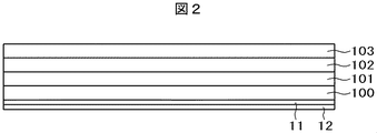
- FIG. 2 is a cross-sectional view taken along line AA of FIG.
- the TFT substrate 100 is formed of resin.
- resins polyimide has excellent properties as a substrate of a display device due to heat resistance, mechanical strength and the like. Therefore, hereinafter, the resin constituting the TFT substrate 100 will be described on the premise of polyimide, but the present invention can also be applied to the case where the TFT substrate 100 is constituted of a resin other than polyimide.
- the thickness of the TFT substrate 100 is, for example, 10 to 20 ⁇ m.
- the TFT circuit layer 101 is formed on the TFT substrate 100.
- the TFT circuit layer 101 is a layer including a scanning line, a video signal line, a power supply line, an organic EL layer which emits light, an anode as a pixel electrode, a cathode as a common electrode, and the like.
- a protective layer 102 is formed to cover the TFT circuit layer 101. Since the characteristics of the organic EL layer change due to moisture or the like, the protective layer 102 prevents the entry of moisture from the outside and mechanically protects the organic EL layer.
- a circularly polarizing plate 103 is attached on the protective layer 102. Since a reflective electrode is formed on the TFT circuit layer 101, it reflects external light. The circularly polarizing plate 103 prevents reflection of external light to improve visibility.
- an adhesive layer 11 formed of metal and a non-thermal expansion layer 12 formed of a material having a small thermal expansion coefficient such as SiO are formed below it. .
- the presence of this layer is a feature of the present invention.
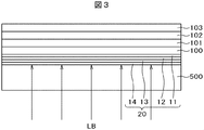
- FIG. 3 is a cross-sectional view illustrating the process of forming the configuration of FIG.
- the TFT substrate 100 is formed of polyimide on the glass substrate 500, but in the present invention, the multilayer film 20 is formed on the glass substrate 500 before the TFT substrate 100 is formed.
- the multilayer film 20 is composed of a photothermal conversion layer 14, a thermal expansion layer 13, a non-thermal expansion layer 12, and an adhesive layer 11 in order from the glass substrate 500 side. The details of these layers are described in FIG.
- a polyimide substrate 100 is formed on the multilayer film 20.
- the polyimide substrate is obtained by applying and baking polyamic acid, which is a precursor of polyimide, with a slit coater or the like.
- polyamic acid which is a precursor of polyimide
- a slit coater or the like On the polyimide substrate 100, a TFT circuit layer 101 that constitutes an essential part of the organic EL display device is formed.
- the configuration of the TFT circuit layer 101 is as described in FIG. After that, the protective layer 102 is formed, and the circularly polarizing plate 103 is attached.
- various elements are formed on a glass substrate 500 in the manufacturing process of the flexible display device.
- the glass substrate 500 has a thickness of 0.5 mm or 0.7 mm which can be easily obtained on the market.
- the glass substrate 500 needs to be removed.
- a laser (LB) is applied to the multilayer film 20, in particular, the photothermal conversion layer.
- FIG. 4 is a cross-sectional view of the multilayer film 20 formed on the glass substrate 500 and the TFT substrate 100.
- the TFT circuit layer and the like formed above the TFT substrate 100 are omitted.
- amorphous silicon (a-Si) is formed on the glass substrate 100 as the light-to-heat conversion layer 14 with a thickness of 50 nm.
- the desirable thickness of a-Si is 40 nm to 80 nm.
- a-Si is formed by CVD (Chemical Vapor Deposition). The role of a-Si is to convert laser light into heat when the laser is irradiated from the glass substrate side.
- the thermal expansion layer 13 receives the heat from the light-to-heat conversion layer 14 and thermally expands to form a stress between itself and the non-thermal expansion layer 12 formed on the upper side. Therefore, the thickness needs to be thick enough to generate stress, for example, 5 nm or more.
- the upper limit is preferably 50 nm or less because it must be thick enough to receive a heat from the light-to-heat conversion layer 14 to cause a sufficient temperature rise.
- a non-thermal expansion layer 12 is formed of, for example, SiO.
- silicon oxide is described as being represented by SiO.
- SiO may be formed by CVD or sputtering.
- the thickness of SiO is 50 nm to 200 nm, but typically 100 nm.
- the non-thermal expansion layer 12 does not cause thermal expansion even when the metal of the lower layer is thermally expanded, and generates stress at the interface between the lower layer and the metal, and after the laser irradiation, the non-thermal expansion layer 12 and the thermal expansion layer 13 To cause peeling between them.
- Another property of the non-thermal expansion layer 12 is a low heat transfer coefficient. That is, the heat of the thermal expansion layer 13 needs not to be conducted to the upper layer, and the temperature of the thermal expansion layer 13 needs to be easily increased.
- a metal layer as the adhesive layer 11 is formed on the non-thermal expansion layer 12.
- the metal layer 11 is formed of, for example, Al having a thickness of 10 nm or less.
- the role of the metal layer 11 is to improve the adhesion to the polyimide layer 100. From this point, the thickness of the adhesive layer 11 needs to be 5 nm or more. Further, from the role of the adhesive layer 11, a thickness of 50 nm or less is sufficient.
- the adhesion layer 11 can use Cr, Ti, etc. other than Al.
- the adhesive layer 11 still exists on the TFT substrate 100 side even after the glass substrate 500 is peeled off.
- the light transmittance of the adhesive layer 11 does not matter, but in the case of the liquid crystal display device described later, it is a transparent film because it is necessary to transmit the light of the backlight.
- it is formed of Al having a thickness of 10 nm or less.
- a polyimide film constituting the TFT substrate 100 is formed with a thickness of 10 ⁇ m to 20 ⁇ m.
- the polyimide film 100 is formed by applying a polyamic acid as a precursor of polyimide with a slit coater or the like and baking it at 300 ° C. to 500 ° C.
- the adhesion of polyimide to glass is not sufficient, when applied directly on the glass substrate 500, the polyimide substrate 100 is easily peeled off, and the process of manufacturing the organic EL display device can not be carried out. In order to prevent peeling of the polyimide substrate 100, an adhesive layer 11 is formed.
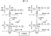
- the reaction shown in FIG. 10 is proposed as a mechanism for increasing the adhesive strength of the polyimide substrate 100. That is, in the process of forming an imide bond from a polyamic acid to a polyimide, an amido group and a carboxyl group to be polymerized originally by an intramolecular reaction are separately bonded to an OH group of AlOOH separately by a dehydration reaction. Although the mechanism is slightly different, the adhesion to the polyimide can be improved even if Cr, Ti or the like is used as the adhesive layer 11.
- the adhesion layer 11 may be simply formed on the glass substrate 500 in terms of simply improving the adhesion between the polyimide substrate and the glass substrate 500. In this case, as described later, the display device is completed. After that, a problem occurs when the glass substrate 500 is peeled off from the TFT substrate 100. According to the present invention, by forming the multilayer film 20 between the glass substrate 500 and the TFT substrate 100, the adhesion strength of the TFT substrate 100 and the glass substrate 500 is maintained in the manufacturing process, and the glass is completed after the display device is completed. A configuration in which peeling of the substrate 500 is compatible can be realized.
- FIG. 5 is a cross-sectional view showing a state in which a laser (LB) is irradiated to separate the glass substrate 500 from the TFT substrate 100.
- the laser is a laser having a wavelength at 308 nm and 355 nm, and the energy density is 90 to 100 mJ / cm 2 . This energy density is not the energy density until melting a-Si.
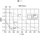
- FIG. 11 is a graph showing the absorption characteristics of laser light in the case of a-Si, poly-Si, and a-IGZO in the case of a film thickness of 50 nm.
- the horizontal axis is the wavelength (nm) and the vertical axis is the absorptivity.
- a-Si and poly-Si absorb 100% for the 308 nm and 355 nm ultraviolet lasers. That is, light-to-heat conversion can be performed effectively by using a laser of this wavelength.
- the heat generated by a-Si which is the light-to-heat conversion layer 14 raises the temperature of the thermal expansion layer 13 formed on the light-to-heat conversion layer 14. Since the thermal conductivity of the glass is very small, most of the heat generated in the light-to-heat conversion layer 14 is absorbed by the thermal expansion layer 13.
- the thermal expansion layer 13 needs to have a large thermal expansion coefficient and a large thermal conductivity. From this point, Al is very suitable as shown in FIG. In addition, Al used may be an alloy to which other metals are added in a small amount.
- the purpose of the light-to-heat conversion layer 14 in the present invention is to supply heat to the thermal expansion layer 13, the energy required to melt the light-to-heat conversion layer 14 is unnecessary. Further, since the glass substrate 500 is separated from the TFT substrate 100 by the stress due to the thermal expansion difference of the thermal expansion layer 13 and the non-thermal expansion layer 12 formed thereon, the metal constituting the thermal expansion layer 13 is used. There is no need to melt it.
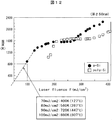
- FIG. 12 shows the energy density F (Laser Fluence mJ / cm 2 ) and the temperature rise of a-Si and poly-Si when a 50 nm thick a-Si is irradiated with a laser having a peak at wavelengths of 308 nm and 355 nm.
- F Laser Fluence mJ / cm 2
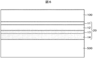
- FIG. 6 is a cross-sectional view showing a state in which a-Si, which is the light-to-heat conversion layer 14, is heated by irradiating a laser, and the heat is conducted to the thermal expansion layer 13 and part of the non-thermal expansion layer 12.
- a-Si which is the light-to-heat conversion layer 14
- the portion shaded with dots indicates the heated portion.
- the heat generated by a-Si is immediately conducted to Al constituting the thermal expansion layer 13.
- SiO constituting the non-thermal expansion layer 12 not only has a small thermal expansion coefficient but also a small thermal conductivity, so heat is not conducted upward.
- the thermal conductivity of Al is 236 (W / mK), while the thermal conductivity of SiO is 1.5 (W / mK).
- the thermal expansion coefficient of Al constituting the thermal expansion layer 13 is 23.1 (10 ⁇ 6 / K), which is much larger than the thermal expansion coefficient 0.5 of SiO (10 ⁇ 6 / K). Therefore, a large stress is generated between the thermal expansion layer 13 and the non-thermal expansion layer 12.
- FIG. 7 is a cross-sectional view showing this situation. That is, almost no heat is conducted, and SiO having a small thermal expansion coefficient hardly expands. On the other hand, since Al having a large thermal conductivity and a large thermal expansion coefficient tries to expand as shown by the arrows, a large stress is generated between SiO and Al.
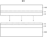
- the laser irradiation time is a short time of 10 n seconds. Then, after the laser irradiation, the thermal expansion layer 13 is rapidly cooled and contracted. Then, a stress reverse to that at the time of expansion is applied to the interface between the thermal expansion layer 13 and the non-thermal expansion layer 12. This situation is shown in FIG. That is, since a stress in different directions is applied to the interface between the thermal expansion layer 13 and the non-thermal expansion layer 12 in a short time, this interface is broken and the interface between the thermal expansion layer 13 and the non-thermal expansion layer 12 It will peel off. This situation is shown in FIG.
- the thermal expansion layer 13 and the light-to-heat conversion layer 14 are removed together with the glass substrate 500, but the adhesive layer 11 and the non-thermal expansion layer 12 remain on the TFT substrate 100 side.
- nonuniformity on the material structure may occur also at the interface between the thermal expansion layer 13 and the non-thermal expansion layer 12, so the thermal expansion layer 13 and the non-thermal expansion layer 12 are partially separated in the actual manufacturing process.
- separation of the glass substrate 500 and the TFT substrate 100 may be performed.
- the adhesive layer 11 is about 10 nm and the non-thermal expansion layer 12 is about 100 nm, there is no problem in the outer shape.
- the light transmittance is not a problem in the organic EL display device. In the case of a liquid crystal display device, the light transmittance of the adhesive layer 11 and the light-to-heat conversion layer 12 is an important issue because a backlight is present, but as described later, the film thickness should be selected. Can solve the problem.
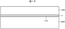
- FIG. 13 to 15 are cross-sectional views for explaining the problem when the present invention is not used.
- FIG. 13 is a cross-sectional view showing a state in which the TFT substrate 100 formed of polyimide is disposed on the glass substrate 500 with the adhesive layer 11 interposed therebetween.
- an adhesion layer 11 formed of a metal such as Al, Cr, or Ti is provided in order to improve the adhesion between the polyimide substrate 100 and the glass substrate 500.
- the thickness of the adhesive layer 11 is, for example, 10 nm.
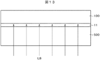
- laser (LB) irradiation is performed on the adhesive layer 11 formed between the glass substrate 500 and the TFT substrate 100 made of polyimide as shown in FIG.
- the peeling is performed by heating the adhesive layer 11 with a laser to melt or vaporize the metal constituting the adhesive layer 11.
- FIG. In this method, since it is necessary to melt the adhesive layer 11, it is necessary to irradiate a laser having an energy density of about 110 to 210 mJ / cm 2 which is larger than the energy density of the laser in the present invention.
- metal reflects laser light with a wavelength of 308 nm to 355 nm, its absorption is as small as about 10 to 50%, and addition of reflected components results in an energy density several times larger than the above energy density.
- the adhesive layer 11 is in a molten state 111 and a part is in a vaporized state 112 by the laser (LB).
- the laser is irradiated for a short time, and after the irradiation, the adhesive layer 11 is rapidly cooled.
- the metal forming the adhesive layer 11 becomes a resolidification layer 113, which causes a phenomenon that the glass substrate 500 and the TFT substrate 100 can not be peeled off.
- the portions other than the adhesive layer 11 are peeled off by the stress utilizing the thermal expansion difference, so that the TFT substrate 100 and the glass substrate 500 can be separated reliably.
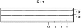
- FIG. 16 is a cross-sectional view of the organic EL display device according to the second embodiment.
- FIG. 16 corresponds to the cross-sectional view along the line AA in FIG. 16 differs from FIG. 2 of the first embodiment in that an aluminum oxide (hereinafter represented by AlO) layer 16 and SiO are formed between the adhesive layer 11 composed of metal and the non-thermal expansion layer 12 composed of SiO. The point is that the layer 15 is formed.
- the AlO layer 16 and the SiO layer 15 are barrier layers against moisture and the like.
- the other configuration of FIG. 16 is the same as that described in FIG.
- FIG. 17 is a cross sectional view showing a process of forming the structure of FIG. 17 differs from FIG. 3 of the first embodiment in that the multilayer film formed between the glass substrate 500 and the TFT substrate 100 has a six-layer structure. That is, the AlO layer 16 and the SiO layer 15 are formed as the barrier layer between the adhesive layer 11 and the non-thermal expansion layer 12.
- a laser (LB) is irradiated to separate the TFT substrate 100 and the glass substrate 500, but this laser is almost absorbed by the light-to-heat conversion layer 14, and the heat is formed on it
- the point absorbed by the expansion layer 13 is also the same as FIG. 3 of the first embodiment.
- FIG. 18 is a cross-sectional view showing the configuration of the TFT substrate 100 and the glass substrate 500 in the second embodiment, and the multilayer film 21 between them. 18 is different from FIG. 4 of the first embodiment in that in the multilayer film 21, an AlO layer 16 and an SiO layer 15 as a barrier layer are formed between the adhesive layer 11 and the non-thermal expansion layer 12. .
- the SiO layer 15 is formed by sputtering or CVD and has a thickness of about 100 nm to 200 nm.
- an AlO layer 16 is formed by sputtering.
- the thickness of the AlO layer 16 is about 50 nm, and the barrier capability is sufficiently exhibited.
- SiO as the non-thermal expansion layer 12 SiO as the non-thermal expansion layer 12, a metal such as Al as the thermal expansion layer 13, and a-Si as the light-to-heat conversion layer 14 are formed.
- the AlO layer 16 is sandwiched between the SiO layer 15 and the SiO layer 12.
- the SiO as the non-thermal expansion layer 12, the metal such as Al as the thermal expansion layer 13, the a-Si as the light-to-heat conversion layer 14 and the like are the same as described in the first embodiment.
- FIG. 19 is a cross-sectional view showing a state in which the light-to-heat conversion layer 14 in the multilayer film 21 is irradiated with a laser (LB) in order to separate the TFT substrate 100 and the glass substrate 500.
- the irradiation conditions of the laser, the mechanism of peeling, and the like are the same as those described in the first embodiment. That is, although the heat generated in the light-to-heat conversion layer 14 is absorbed by the thermal expansion layer 13, SiO, which is the non-thermal expansion layer 12 formed on the thermal expansion layer 13, has a small thermal conductivity, Heat is not conducted above the expansion layer 12. Therefore, the thermal effects on the AlO layer 16 and the SiO layer 15 formed above the non-thermal expansion layer 12 can be ignored.
- FIG. 20 is a cross-sectional view showing a state in which the glass substrate 500 is separated from the TFT substrate 100 by laser irradiation.
- the adhesive layer 11, the AlO layer 16 as a barrier layer, the SiO layer 15, and the non-thermal expansion layer 12 are present on the TFT substrate 100 side.
- both are thin films, they do not pose a problem in terms of dimensions.
- the organic EL display does not have a backlight, there is no optical problem.
- the thermal expansion layer 13 and the light-to-heat conversion layer 14 are present on the glass substrate side as in the first embodiment.
- the amount of water or the like which penetrates through the polyimide from the outside can be greatly suppressed, so that the deterioration of the organic EL layer can be prevented and the reliability can be improved. It can.
- the influence of moisture and the like from the outside can be reduced to suppress the characteristic variation of the TFT.
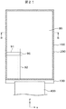
- FIG. 21 is a plan view of the liquid crystal display device.
- the TFT substrate 100 and the counter substrate 200 are bonded by a sealant 150, and liquid crystal is held between the TFT substrate 100 and the counter substrate 200 inside the sealant 150.
- a display area 90 is formed in the portion where the TFT substrate 100 and the counter substrate 200 overlap.
- scanning lines 91 extend in the horizontal direction (x direction) and are arranged in the vertical direction (y direction).
- the video signal lines 92 extend in the vertical direction and are arranged in the horizontal direction.
- Pixels 95 are formed in a region surrounded by the scanning line 91 and the video signal line 92.
- the TFT substrate 100 is formed to be larger than the counter substrate 200, and a portion where the TFT substrate 100 and the counter substrate 200 do not overlap each other is a terminal region.
- the terminal area is connected to a flexible wiring board 400 for supplying power and signals to the liquid crystal display device.
- FIG. 22 is a cross-sectional view taken along a line BB in FIG.
- a TFT circuit layer 101 is formed on a TFT substrate 100 formed of polyimide, and a color filter layer 201 is formed on an opposing substrate 200 formed of polyimide.
- the TFT substrate 100 and the counter substrate 200 are bonded by a sealing material 150, and a liquid crystal 300 is sealed inside the sealing material 150.
- the adhesive layer 11 and the non-thermal expansion layer 12 described in the first embodiment are formed on the outside of the TFT substrate 100 and the counter substrate 200.
- the upper polarizing plate 220 is attached to the outside of the adhesive layer 11 and the non-thermal expansion layer 12 on the counter substrate 200 side, and the lower polarizing plate 120 is on the outer side of the adhesive layer 11 and the non-thermal expansion layer 12 on the TFT substrate 100 side. It is pasted.
- a backlight 600 is formed on the back of the lower polarizing plate 120.
- the backlight 600 can maintain flexibility as the whole liquid crystal display device by using a sheet-like light source formed of an organic EL or the like.
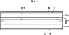
- FIG. 23 is a cross-sectional view of the liquid crystal display panel with the upper polarizing plate 220 and the lower polarizing plate 120 removed.
- a metal layer as the adhesive layer 11 and an SiO layer as the non-thermal expansion layer 12 are formed on the outside of the TFT substrate 100 and the outside of the counter substrate 200.
- a TFT circuit layer is formed on a TFT substrate 100 formed on a glass substrate 500, and an opposing substrate 200 formed on a glass substrate 500.
- the color filter layer 201 and the like are formed, and in this state, the liquid crystal 300 is filled, and the TFT substrate 100 and the counter substrate 200 are adhered by the sealing material 150 to seal the liquid crystal 300.
- the adhesive layer 11, the non-thermal expansion layer 12, the thermal expansion layer 13, and the light-to-heat conversion layer 14 are provided between the TFT substrate 100 and the glass substrate 500 and between the counter substrate 200 and the glass substrate 500.
- a multilayer film 20 is formed. The configuration and function of each layer are the same as described in the first embodiment.
- the light-to-heat conversion layer 14 is irradiated with a laser (LB) to thermally expand the thermal expansion layer 13 and then thermally shrink, thereby generating stress with the non-thermal expansion layer 12.
- LB laser
- the glass substrate 500 is separated from the TFT substrate 100 or the counter substrate 200.
- the irradiation conditions of the laser, the mechanism of peeling, and the like are the same as those described in the first embodiment.
- the liquid crystal display device is different from the organic EL display device in that a backlight is used. That is, the adhesive layer 11 and the non-thermal expansion layer 12 formed on the TFT substrate 100 and the counter substrate 200 need to transmit visible light.
- the non-thermal expansion layer 12 is formed of SiO.
- FIG. 26 is a graph showing the light transmittance of a 10 mm thick SiO film.
- the horizontal axis is the wavelength
- the vertical axis is the transmittance.
- the transmittance of SiO is 90% even if the thickness is 10 mm. 90% is due to the refractive index at the interface. Therefore, the transmittance of SiO constituting the non-thermal expansion layer 12 has no problem with the screen brightness.
- the adhesive layer 11 is formed of a metal such as Al, Cr, or Ti.
- Al even metal, becomes transparent when the film thickness becomes 10 nm or less.
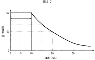
- FIG. 27 shows transmittance characteristics of Al for visible light. The visible light in this case refers to the green wavelength (500 nm).
- the horizontal axis is the Al film thickness
- the vertical axis is the transmittance.
- the transmittance of Al is 100% up to 10 nm, and the transmittance decreases when it exceeds 10 nm. Therefore, if an Al layer of 10 nm or less is used as the adhesive layer, the influence on the light transmittance can be ignored.
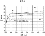
- FIG. 28 is a graph showing the transmittance for each wavelength when the thickness of Cr, Nb, Ni, Ta or the like is 6.5 nm.
- the horizontal axis is the wavelength
- the vertical axis is the transmittance.
- the transmittance is about 50% even if the thickness is 6.5 nm. Therefore, in the case of a liquid crystal display device, using Cr or the like as the adhesive layer 11 has a problem. However, there is no problem in the case of the organic EL display device.
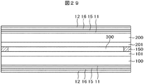
- FIG. 29 is a cross-sectional view of the liquid crystal display panel in the fourth embodiment.
- FIG. 29 is a cross-sectional view corresponding to FIG. 23 of the third embodiment. 29 differs from FIG. 23 in that the adhesive layer 11, the SiO layer 15 forming a barrier layer, the AlO layer 16 forming a barrier layer, and the non-thermal expansion layer 12 outside the TFT substrate 100 and the counter substrate 200. The point is that a four-layered laminated film is formed.
- the configuration of the laminated film in FIG. 29 is the same as the configuration of the laminated film on the outside of the TFT substrate 100 in Example 2 of the organic EL display device.
- a TFT substrate 100 formed on a glass substrate 500 and an opposite substrate 200 formed on a glass substrate 500 are formed.
- the liquid crystal 300 is sealed by bonding the TFT substrate 100 and the counter substrate 200 with the sealant 150.
- the adhesive layer 11, the SiO layer 15 as a barrier layer, the AlO layer 16 as a barrier layer, and no heat are formed between the TFT substrate 100 and the glass substrate 500 and between the counter substrate 200 and the glass substrate 500.
- a multilayer film 21 composed of the expansion layer 12, the thermal expansion layer 13, and the light-to-heat conversion layer 14 is formed. The configuration and function of each layer are the same as described in the second embodiment.
- the thermal expansion layer 13 is thermally expanded and shrunk rapidly with respect to the non-thermal expansion layer 12 by irradiating the light-to-heat conversion layer 14 with a laser (LB).
- the layer 13 and the non-thermal expansion layer 12 are peeled off, and the glass substrate 500 is separated from the TFT substrate 100 or the counter substrate 200.
- the irradiation conditions of the laser, the mechanism of peeling, and the like are the same as those described in the first embodiment.
- the liquid crystal display device is different from the organic EL display device in that a backlight is used.
- the adhesive layer 11 and the thermal expansion layer 12 are as described in the third embodiment.
- an SiO layer 15 as a barrier layer and an AlO layer 16 as a barrier layer are further formed.
- the SiO layer has almost no influence on the visible light transmittance, as shown in FIG. Further, in the visible region, the transmittance of the AlO layer is 90% even if it includes the reflection at the interface, and the influence on the transmittance can be almost ignored.
- the present invention can be applied without any problem if the metal material of the adhesive layer 11 is noted.
- FIG. 32 is a table summarizing the thermal properties of the materials associated with the present specification.
- the combination of Al as the material used as the thermal expansion layer 13 and SiO used as the material of the non-thermal expansion layer 12 has very excellent effects for the present invention.
- the light-to-heat conversion layer 14 is described as being a-Si.
- poly-Si also absorbs 100% for ultraviolet light having a wavelength of 308 nm and 355 nm. Therefore, poly-Si can also be used as the light-to-heat conversion layer.
- the contact bonding layer 11 for example, even if it is aluminum oxide AlO which is a metal oxide, adhesiveness can be raised. That is, as shown in FIG. 10, when AlOOH is present in the adhesive layer 11, this OH group bonds with an amide group and a carboxyl group in the polyimide by a dehydration reaction to form a strong bond between the polyimide and AlO. It is because it can.
- AlO is transparent to visible light
- the degree of freedom in selecting the thickness of the adhesive layer 11 can be increased.
- the transparent conductive film ITO also has OH groups on the surface and is transparent to visible light, it can be applied in the same manner as AlO.
Landscapes
- Physics & Mathematics (AREA)
- General Physics & Mathematics (AREA)
- Engineering & Computer Science (AREA)
- Nonlinear Science (AREA)
- Crystallography & Structural Chemistry (AREA)
- Chemical & Material Sciences (AREA)
- Theoretical Computer Science (AREA)
- Optics & Photonics (AREA)
- Manufacturing & Machinery (AREA)
- Mathematical Physics (AREA)
- Electroluminescent Light Sources (AREA)
- Devices For Indicating Variable Information By Combining Individual Elements (AREA)
- Liquid Crystal (AREA)
- Laminated Bodies (AREA)
Abstract
本発明の目的は、樹脂基板を有するフレキシブル表示装置を高歩留まりで形成することである。構成は次のとおりである。樹脂基板100に画素が形成された表示装置の製造方法であって、ガラス基板500上に半導体で形成される第1の層14を形成し、前記第1の層の上に第1の金属からなる第2の層13を形成し、前記第2の層の上に第1の絶縁物からなる第3の層12を形成し、前記第3の層の上に、第2の金属または金属酸化物からなる第4の層11を形成し、前記第4の層11の上に、ポリイミドの前駆体を塗布し、焼成して、ポリイミド基板100を形成し、前記ポリイミド基板の上に前記画素を形成し、その後、前記第1の層にレーザLBを照射することにより、前記第2の層13と前記第3の層12間で剥離を生じさせることによって、前記ポリイミド基板100と前記ガラス基板500を分離することを特徴とする表示装置の製造方法。
Description
本発明は表示装置に係り、特に基板を湾曲させることができるフレキシブル表示装置及びその製造方法に関する。
有機EL表示装置や液晶表示装置は表示装置を薄くすることによって、湾曲させて使用することができる。また、基板をポリイミド等の樹脂によって形成することによってフレキシブルな表示装置とすることができる。
樹脂で形成された基板には、導電層、絶縁層、保護層、電極層等多くの膜が積層される。このように多数の膜を形成する場合、光の透過率が問題になる。特許文献1には、金属層と誘電体層を交互に重ねあわせた積層体によるNDF(Neutral Density Filter)が記載されている。また、金属膜も薄膜とすると、可視光に対する透過率が上昇する。特許文献2には、アルミニウム(Al)膜を薄膜にした場合の透過率の変化が記載されている。
フレキシブル表示装置に用いられる樹脂基板は10μm乃至20μmである。このような薄い基板は、例えば、ガラス基板上に液体状の樹脂を塗布し、焼成して、樹脂基板にする。そして、樹脂基板は、ガラス基板とともに、製造工程を通り、表示パネルとして完成した後、ガラス基板が樹脂基板から剥離され、フレキシブル表示装置が完成する。
このようなプロセスでは、次のような問題点がある。第1は、製造工程を通過する間は、樹脂基板はガラス基板と確実に接着している必要がある。第2に、表示装置が完成した後は、樹脂基板からガラス基板を確実に剥離することが可能であることである。
しかし、樹脂とガラス基板との接着力は、一般的には弱い。また、樹脂基板とガラス基板を強固に接着したとしても、表示装置が完成後、樹脂基板とガラス基板を確実に分離できるとは限らない。
本発明の課題は、ガラス基板上に樹脂基板を形成し、該樹脂基板の上に導電層や絶縁層等を形成したフレキシブル表示装置において、製造工程では、樹脂基板とガラス基板は確実に接着し、表示装置が完成した後は、ガラス基板を樹脂基板から確実に分離することが出来る表示装置の構成を実現することである。
本発明は上記課題を克服するものであり、代表的な手段は次のとおりである。
(1)樹脂基板に画素が形成された表示装置であって、前記樹脂基板の前記画素とは逆側の層に金属または金属酸化物からなる第1の層が形成され、前記第1の層の上に第1の絶縁物からなる第2の層が形成されていることを特徴とする表示装置。
(2)前記第2の層の上に、前記第2の絶縁物からなる第3の層が形成され、前記第3の層の上に、第3の絶縁物からなる第4の層が形成されていることを特徴とする(1)請求項1に記載の表示装置。
(3)樹脂基板に画素が形成された表示装置の製造方法であって、ガラス基板上に半導体で形成される第1の層を形成し、前記第1の層の上に第1の金属からなる第2の層を形成し、前記第2の層の上に第1の絶縁物からなる第3の層を形成し、前記第3の層の上に、第2の金属または金属酸化物からなる第4の層を形成し、前記第4の層の上に、ポリイミドの前駆体を塗布し、焼成して、ポリイミド基板を形成し、前記ポリイミド基板の上に前記画素を形成し、その後、前記第1の層にレーザを照射することにより、前記第2の層と前記第3の層間で剥離を生じさせることによって、前記ポリイミド基板と前記ガラス基板を分離することを特徴とする表示装置の製造方法。
(4)樹脂基板に画素が形成された表示装置の製造方法であって、ガラス基板上に半導体で形成される第1の層を形成し、前記第1の層の上に第1の金属からなる第2の層を形成し、前記第2の層の上に第1の絶縁物からなる第3の層を形成し、前記第3の層の上に、第2の絶縁物からなる第4の層を形成し、前記第4の層の上に第3の絶縁物からなる第5の層を形成し、前記第5の層の上に第2の金属、または、金属酸化物からなる第6の層を形成し、前記第6の層の上に、ポリイミドの前駆体を塗布し、焼成して、ポリイミド基板を形成し、前記ポリイミド基板の上に前記画素を形成し、その後、前記第1の層にレーザを照射することにより、前記第2の層と前記第3の層間で剥離を生じさせることによって、前記ポリイミド基板と前記ガラス基板を分離することを特徴とする表示装置の製造方法。
以下に実施例を用いて本発明の内容を詳細に説明する。
図1は本発明が適用される有機EL表示装置の平面図である。本発明の有機EL表示装置は、フレキシブルに湾曲させることが出来る表示装置である。したがって、TFT(Thin Film Transistor)、走査線、電源線、映像信号線、画素電極、有機EL発光層等が形成されているTFT基板100は樹脂で形成されている。
図1において、表示領域90の両側には走査線駆動回路80が形成されている。表示領域90には、横方向(x方向)に走査線91が延在し、縦方向(y方向)に配列している。映像信号線92及び電源線93が縦方向に延在し、横方向に配列している。走査線91と、映像信号線92及び電源線93で囲まれた領域が画素95となっており、画素95内には、TFTで形成された駆動トランジスタ、スイッチングトランジスタ、光を発光する有機EL発光層等が形成されている。
図2は図1のA-A断面図である。図2において、TFT基板100は樹脂で形成されている。樹脂の中でもポリイミドは、耐熱性、機械的強度等から、表示装置の基板としては優れた特性を有している。したがって、以後は、TFT基板100を構成する樹脂としては、ポリイミドを前提として説明するが、本発明は、ポリイミド以外の樹脂でTFT基板100を構成した場合にも適用することが出来る。TFT基板100の厚さは例えば10乃至20μmである。
TFT基板100の上には、TFT回路層101が形成されている。TFT回路層101は、走査線、映像信号線、電源線、光を発光する有機EL層、画素電極としてのアノード、共通電極としてのカソード等を含む層である。TFT回路層101を覆って保護層102が形成されている。有機EL層は、水分等によって特性が変動するので、保護層102は、外部からの水分の侵入を防止し、また、有機EL層を機械的に保護する。
保護層102の上には、円偏光板103が貼り付けられている。TFT回路層101には、反射電極が形成されているので、これが外光を反射する。円偏光板103は、外光の反射を防止して、視認性を向上させる。
図2において、TFT基板100の下には、金属で形成された接着層11と、その下には、SiO等の熱膨張係数の小さい物質で形成された非熱膨張層12が形成されている。この層の存在が本発明の特徴となっている。
図3は、図2の構成を形成するプロセスを示す断面図である。図3において、ガラス基板500の上にポリイミドによってTFT基板100を形成するが、本発明は、TFT基板100を形成する前に、ガラス基板500上に多層膜20を形成する。多層膜20は、ガラス基板500側から順に、光熱変換層14、熱膨張層13、非熱膨張層12、接着層11から構成されている。これらの層の詳細は図4で説明する。
図3において、多層膜20の上にポリイミド基板100が形成されている。ポリイミド基板は、ポリイミドの前駆体であるポリアミック酸をスリットコータ等で塗布し、焼成したものである。ポリイミド基板100の上に、有機EL表示装置の本質部分を構成するTFT回路層101が形成されている。TFT回路層101の構成は図2で説明したとおりである。その後、保護層102を形成し、円偏光板103を貼り付ける。
図3に示すように、フレキシブル表示装置の製造工程では、ガラス基板500の上に種々の要素が形成される。ガラス基板500は、市場で容易に調達可能な0.5mm、あるいは、0.7mmの厚さのものが使用される。しかし、フレキシブル表示装置が形成された後は、ガラス基板500を除去する必要がある。図3において、レーザ(LB)を多層膜20、特に、光熱変換層14に照射する。多層膜20内の熱膨張層13と非熱膨張層12の層間を剥離することにより、TFT基板100とガラス基板500を分離する。
図4乃至図9でこのメカニズムを詳細に説明する。なお、有機EL表示装置、あるいは、液晶表示装置は、個々の表示装置を単独で形成したのでは、効率が悪いので、マザー基板に多くの表示パネルを形成し、その後分離することが行われる。以後の説明は、個々の表示領域の場合について行うが、マザー基板の場合も同様である。
図4は、ガラス基板500の上に形成された多層膜20とTFT基板100の断面図である。図4乃至図9では、TFT基板100より上に形成されたTFT回路層等は省略されている。図4において、ガラス基板100の上に光熱変換層14として、非晶質シリコン(a-Si)が厚さ50nmで形成されている。a-Siの望ましい厚さは40nm乃至80nmである。a-SiはCVD(Chemical Vapour Deposition)で形成される。a-Siの役割は、ガラス基板側からレーザが照射された場合に、レーザ光を熱に変換することである。
光熱変換層14の上に熱膨張層13として例えばAlがスパッタリングによって10nm程度形成されている。熱膨張層13は、光熱変換層14からの熱を受けて熱膨張し、上側に形成される非熱膨張層12との間にストレスを形成することである。したがって、厚さは、ストレスを発生することが出来る程度の厚さが必要であり、例えば、5nm以上必要である。一方、上限は、光熱変換層14からの熱を受けて十分温度上昇を生ずる程度の厚さでなければならないので、50nm以下であることが望ましい。
熱膨張層13の上に、非熱膨張層12が例えばSiOによって形成される。なお、本明細書は、酸化シリコンをSiOで代表させて記載する。SiOはCVDで形成してもよいし、スパッタリングで形成してもよい。SiOの厚さは、50nm乃至200nmであるが、代表的には100nmである。非熱膨張層12は、下層の金属が熱膨張しても、熱膨張を起こさず、下層と金属との界面でストレスを発生し、レーザ照射後に、非熱膨張層12と熱膨張層13との間で剥離を生じさせることである。
非熱膨張層12の他の特性は、熱伝導係数が小さいことである。すなわち、熱膨張層13の熱を上層に伝導させず、熱膨張層13が温度上昇しやすくする必要があるからである。
非熱膨張層12の上には、接着層11としての金属層が形成されている。金属層11は、例えば、厚さが10nm以下のAlで形成されている。金属層11の役割は、ポリイミド層100との接着性を向上させるためである。この点から接着層11の厚さは5nm以上である必要がある。また、接着層11としての役割から、厚さは50nm以下で十分である。接着層11はAlの他、Cr,Ti等を使用することが出来る。
一方、接着層11は、ガラス基板500を剥離した後も、TFT基板100側に存在している。有機EL表示装置の場合は、接着層11の光透過率は問題にならないが、後で説明する液晶表示装置の場合には、バックライトの光を通す必要があるので、透明膜となっている必要があり、このためには、例えば、厚さが10nm以下のAlで形成される。
図4において、接着層11の上には、TFT基板100を構成するポリイミド膜が10μm乃至20μmの厚さで形成される。ポリイミド膜100は、ポリイミドの前駆体としてのポリアミック酸をスリットコータ等で塗布し、300℃乃至500℃で焼成して形成する。
ポリイミドはガラスとの接着性は充分ではないので、ガラス基板500の上に直接塗布すると、ポリイミド基板100は容易に剥離し、有機EL表示装置の製造工程を通すことが出来ない。ポリイミド基板100の剥離を防止するために、接着層11が形成される。
接着層11としてAlを用いた場合において、ポリイミド基板100の接着強度が増大するメカニズムとして、図10に示す反応が提唱されている。すなわち、ポリアミック酸からポリイミドにイミド結合する過程において、本来分子内反応で高分子化すべきアミド基とカルボシキル基がそれぞれ、別個にAlOOHのOH基と脱水和反応によって結合した構造である。メカニズムは若干異なるが、CrやTi等を接着層11として用いても、ポリイミドとの接着力を向上させることが出来る。
単に、ポリイミド基板とガラス基板500との接着力を向上させるという意味では、接着層11をガラス基板500上に形成するだけでもよいが、この場合、後で説明するように、表示装置が完成した後、ガラス基板500をTFT基板100から剥離する場合に問題が生ずる。本発明は、ガラス基板500とTFT基板100との間に多層膜20を形成することによって、製造工程におけるTFT基板100とガラス基板500の接着強度の維持と、表示装置が完成した後の、ガラス基板500の剥離を両立させる構成を実現することが出来る。
図5は、TFT基板100からガラス基板500を剥離するために、レーザ(LB)を照射している状態を示す断面図である。レーザは、波長が308nm及び355nmにピークを有するレーザであり、エネルギー密度は、90乃至100mJ/cm2である。このエネルギー密度は、a-Siを溶融させるまでのエネルギー密度ではない。
図11は膜厚が50nmの場合の、a-Si、poly-Si、a-IGZOの場合のレーザ光の吸収特性を示すグラフである。図11において、横軸は波長(nm)であり、縦軸は吸収率である。図11に示すように、a-Siおよびpoly-Siは、308nm、355nmの紫外線レーザについては、100%吸収する。つまり、この波長のレーザを用いることによって、効果的に光―熱変換を行うことが出来る。
このように、光熱変換層14であるa-Siで発生した熱は、光熱変換層14の上に形成された熱膨張層13の温度を上昇させる。ガラスの熱伝導率は非常に小さいので、光熱変換層14で発生した熱は、殆どが熱膨張層13に吸収される。熱膨張層13は、熱膨張係数が大きく、かつ熱伝導率が大きいことが必要である。この点からは、図32に示すように、Alが非常に適している。なお、使用するAlは、他の金属が少量添加された合金であってもよい。
本発明における光熱変換層14は、熱膨張層13に熱を供給することが目的であるから、光熱変換層14を溶融させるまでのエネルギーは不要である。また、熱膨張層13とその上に形成される非熱膨張層12の熱膨張差によるストレスによって、ガラス基板500をTFT基板100から分離するものであるから、熱膨張層13を構成する金属を溶融させる必要もない。
図12は、厚さ50nmのa-Siに波長が308nm及び355nmにピークを有するレーザを照射した場合のエネルギー密度F(Laser Fluence mJ/cm2)と、a-Si及びpoly-Siの温度上昇の関係を示すグラフである。図12において、横軸はレーザのエネルギー密度F(mJ/cm2)であり、縦軸はa-Siあるいはpoly-Siの温度である。
図12の下側に示すように、レーザのエネルギー密度が90(mJ/cm2)のとき、a-Siの温度は447℃であり、エネルギー密度が100(mJ/cm2)のとき、a-Siの温度は607℃である。Alの融点は660℃であるから、レーザのエネルギー密度が100(mJ/cm2)のとき、仮に熱膨張層13の温度が光熱変換層14を構成するa-Siと同じ温度になったとしても、Alが融解することは無い。しかし、Alは大きな熱膨張を起こす。
図6はレーザを照射し、光熱変換層14であるa-Siが加熱され、その熱が熱膨張層13、および、非熱膨張層12の一部に伝導した状態を示す断面図である。図6において、ドットでシェーディングした部分が加熱された部分を示している。a-Siで発生した熱は、熱膨張層13を構成するAlにはすぐに伝導する。しかし、非熱膨張層12を構成するSiOは、熱膨張率が小さいのみでなく、熱伝導率も小さいので、熱は上側に伝導しない。図32に示すように、Alの熱伝導率は、236(W/mK)であるのに対し、SiOの熱伝導率は1.5(W/mK)である。
したがって、a-Siから伝導してきた熱は殆どが熱膨張層13を膨張させるために使用される。さらに、熱膨張層13を構成するAlの熱膨張係数は、23.1(10-6/K)であり、SiOの熱膨張係数0.5(10-6/K)よりもはるかに大きい。したがって、熱膨張層13と非熱膨張層12の間には大きなストレスが発生することになる。
図7はこの様子を示す断面図である。つまり、殆ど熱が伝導せず、かつ、熱膨張係数も小さなSiOは殆ど膨張しない。一方、熱伝導率が大きく、熱膨張係数も大きいAlは矢印のように膨張しようとするので、SiOとAlの間には大きなストレスが発生する。
一方、レーザ照射時間は、10n秒単位の短い時間である。そして、レーザ照射後は、熱膨張層13は急激に冷却し収縮する。そうすると、熱膨張層13と非熱膨張層12の界面には、膨張時と逆なストレスが加わる。この様子を図8に示す。つまり、熱膨張層13と非熱膨張層12の界面には、方向の異なるストレスが短時間に印加されるので、この界面は破壊され、熱膨張層13と非熱膨張層12との界面で剥離することになる。この様子を図9に示す。
図9に示すように、熱膨張層13と光熱変換層14はガラス基板500とともに除去されるが、接着層11と非熱膨張層12はTFT基板100側に残る。ただし、一般には熱膨張層13と非熱膨張層12との界面においても材料組織上の不均一が生じうるため、実際の製造工程では部分的に熱膨張層13と非熱膨張層12が分離しない状態でガラス基板500とTFT基板100との分離が行われることもありうる。接着層11は10nm、非熱膨張層12は100nm程度なので、外形上で問題になることは無い。光透過率も、有機EL表示装置では問題になることは無い。液晶表示装置の場合は、バックライトが存在するので、接着層11と光熱変換層12の光透過率は重要な問題になるが、これも、後で説明するように、膜厚を選定することによって問題を解決することが出来る。
図13乃至図15は、本発明を使用しない場合の問題を説明する断面図である。図13は、ガラス基板500の上に接着層11を介してポリイミドによって形成されたTFT基板100を配置した状態を示す断面図である。図13において、ポリイミド基板100とガラス基板500との接着力を向上させるために、Al、Cr、Ti等の金属で形成された接着層11を設ける。接着層11の厚さは例えば、10nmである。
この状態で製造プロセスを通り、有機EL表示装置が完成した後、図13に示すように、ガラス基板500とポリイミドによるTFT基板100の間に形成された接着層11にレーザ(LB)照射することによって、ガラス基板500とTFT基板100を剥離する。この剥離は、レーザによって、接着層11を加熱し、接着層11を構成する金属を溶融あるいは気化させることによって剥離する。この様子を図14に示す。この方法では、接着層11を溶融させる必要があるので、本発明でのレーザのエネルギー密度よりも大きく、110乃至210mJ/cm2程度のエネルギー密度のレーザを照射する必要がある。さらに、金属は波長308nm乃至355nmのレーザ光を反射するため吸収が約10~50%と小さく、反射分を加算すると前記のエネルギー密度の数倍の大きいエネルギー密度となる。
図14において、レーザ(LB)によって、接着層11が溶融状態111になり、また、一部は気化状態112となっている。しかし、レーザは短時間照射され、照射後は、接着層11は急冷する。そうすると、図15に示すように、接着層11を構成する金属は再凝固層113となり、ガラス基板500とTFT基板100とを剥離できないという現象を生ずる。これに対して、本発明は、上記のように、接着層11以外の部分において、熱膨張差を利用したストレスによって剥離するので、確実にTFT基板100とガラス基板500を分離することが出来る。
図16は実施例2による有機EL表示装置の断面図である。図16は図1のA-A断面図に対応する。図16が実施例1の図2と異なる点は、金属で構成される接着層11とSiOで構成される非熱膨張層12の間に、酸化アルミニウム(以後AlOで代表させる)層16とSiO層15が形成されている点である。AlO層16とSiO層15は、水分等に対するバリア層である。図16のその他の構成は図2で説明したのと同じである。
図17は、図16の構成を形成するプロセスを示す断面図である。図17が実施例1の図3と異なる点は、ガラス基板500とTFT基板100との間に形成される多層膜が6層構成になっている点である。すなわち、接着層11と非熱膨張層12との間にバリア層としての、AlO層16とSiO層15が形成されている。
図17において、TFT基板100とガラス基板500を分離するために、レーザ(LB)が照射されているが、このレーザは、光熱変換層14で殆ど吸収され、この熱が上に形成される熱膨張層13に吸収される点も実施例1の図3と同様である。
図18は実施例2におけるTFT基板100とガラス基板500と、その間の多層膜21の構成を示す断面図である。図18が実施例1の図4と異なる点は、多層膜21において、接着層11と非熱膨張層12の間にバリア層としてのAlO層16とSiO層15が形成されていることである。SiO層15はスパッタリングあるいはCVDで形成され、厚さは100nm乃至200nm程度である。
SiO層15の下にはAlO層16がスパッタリングで形成されている。AlO層16の厚さは、50nm程度でバリア能力は充分に発揮されるが、100nm程度形成できればなお良い。AlO層16の下には、非熱膨張層12としてのSiO、熱膨張層13としてのAl等の金属、光熱変換層14としてのa-Siが形成されている。図18の構成は、AlO層16がSiO層15及びSiO層12でサンドイッチされた構成となっている。非熱膨張層12としてのSiO、熱膨張層13としてのAl等の金属、光熱変換層14としてのa-Si等は実施例1で説明したのと同様である。
図19は、TFT基板100とガラス基板500を分離するために、多層膜21における光熱変換層14にレーザ(LB)を照射している状態を示す断面図である。レーザの照射条件、剥離のメカニズム等は、実施例1で説明したのと同様である。すなわち、光熱変換層14で発生した熱は、熱膨張層13に吸収されるが、熱膨張層13の上に形成された非熱膨張層12であるSiOは熱伝導率が小さいので、非熱膨張層12よりも上側には熱を伝えない。したがって、非熱膨張層12より上側に形成されたAlO層16およびSiO層15への熱的な影響は無視することが出来る。
図20は、レーザ照射によって、ガラス基板500がTFT基板100から分離された状態を示す断面図である。図20において、接着層11、バリア層としてのAlO層16、SiO層15、および非熱膨張層12がTFT基板100側に存在している。しかし、いずれも薄膜なので、寸法的には問題にはならない。また、有機EL表示装置はバックライトが存在しないため、光学的にも問題になることは無い。一方、ガラス基板側には、実施例1と同様、熱膨張層13および光熱変換層14が存在している。
実施例2では、実施例1の効果に加え、外部からポリイミドを通して侵入してくる水分等の量を大幅に抑えることが出来るので、有機EL層の劣化を防止し、信頼性を向上させることが出来る。また、TFTを酸化物半導体で形成する場合は、外部からの水分等の影響を軽減し、TFTの特性変動を抑えることが出来る。
本発明は、液晶表示装置にも適用することが出来る。液晶表示装置についても、フレキシブル表示装置としたいという要求がある。図21は液晶表示装置の平面図である。図21において、TFT基板100と対向基板200がシール材150によって接着し、シール材150の内側で、TFT基板100と対向基板200の間に液晶が挟持されている。
TFT基板100と対向基板200が重なった部分に表示領域90が形成されている。表示領域90には、走査線91が横方向(x方向)に延在し、縦方向(y方向)に配列している。また、映像信号線92が縦方向に延在し、横方向に配列している。走査線91と映像信号線92で囲まれた領域に画素95が形成されている。TFT基板100は対向基板200よりも大きく形成され、TFT基板100と対向基板200が重なっていない部分は端子領域となっている。端子領域は、液晶表示装置に電源や信号を供給するためのフレキシブル配線基板400が接続している。
図22は、図21のB-B断面図である。図22において、ポリイミドで形成されたTFT基板100には、TFT回路層101が形成され、ポリイミド形成された対向基板200には、カラーフィルタ層201が形成されている。TFT基板100と対向基板200はシール材150によって接着し、シール材150の内側に液晶300が封止されている。
図22において、TFT基板100および対向基板200の外側には、実施例1で説明した接着層11および非熱膨張層12が形成されている。対向基板200側の接着層11および非熱膨張層12の外側には上偏光板220が貼り付けられ、TFT基板100側の接着層11および非熱膨張層12の外側には下偏光板120が貼り付けられている。
図22において、下偏光板120の背面にバックライト600が形成されている。バックライト600は有機EL等で形成されたシート状の光源を使用することにより、液晶表示装置全体としてもフレキシビリティを維持することが出来る。
図23は、上偏光板220および下偏光板120を取り除いた状態における液晶表示パネルの断面図である。図23において、TFT基板100の外側及び対向基板200の外側には、接着層11としての金属層、および、非熱膨張層12としてのSiO層が形成されている。このような液晶表示パネルを形成するには、図24に示すように、ガラス基板500に形成されたTFT基板100の上にTFT回路層を形成し、ガラス基板500に形成された対向基板200にカラーフィルタ層201等を形成し、この状態で、液晶300を充填し、シール材150によってTFT基板100と対向基板200を接着して液晶300を封止する。
この状態においては、TFT基板100とガラス基板500の間、及び、対向基板200とガラス基板500の間には接着層11、非熱膨張層12、熱膨張層13、光熱変換層14からのなる多層膜20が形成されている。各層の構成と作用は実施例1で説明したのと同様である。
その後、図25に示すように、光熱変換層14にレーザ(LB)を照射して熱膨張層13を熱膨張させ、その後熱収縮させることにより、非熱膨張層12との間にストレスを発生させることによって、ガラス基板500をTFT基板100あるいは対向基板200から分離する。レーザの照射条件、剥離のメカニズム等は実施例1で説明したのと同様である。
図23に戻り、液晶表示装置が有機EL表示装置と異なる点はバックライトを用いているという点である。すなわち、TFT基板100および対向基板200に形成された接着層11、非熱膨張層12等は、可視光を透過させる必要がある。図23において、非熱膨張層12はSiOで形成されている。図26は厚さが10mmのSiO膜の光透過率を示すグラフである。
図26において、横軸は波長、縦軸は透過率である。図26に示すように、可視光の範囲では、厚さが10mmであっても、SiOの透過率は90%である。90%は界面での屈折率に起因するものである。したがって、非熱膨張層12を構成するSiOの透過率は、画面輝度には全く問題はない。
一方、接着層11は、Al、Cr、Ti等の金属で形成されている。金属でもAlは膜厚が10nm以下になると透明になる。図27は可視光についてのAlの透過率特性である。この場合の可視光は緑波長(500nm)を言う。図27において、横軸はAl膜厚であり、縦軸は透過率である。図27の矢印で示すように、Alの透過率は10nmまでは100%であり、10nmを超えると透過率が低下してくる。したがって、接着層として10nm以下のAl層を用いれば光透過率への影響は無視することが出来る。
図28は、Cr、Nb、Ni、Ta等の厚さが6.5nmの場合における波長毎の透過率を示すグラフである。図28において、横軸は波長、縦軸は透過率である。図28において、Crに着目すると、可視光領域においては、厚さが6.5nmであっても、透過率は50%前後である。したがって、液晶表示装置の場合には、Cr等を接着層11として用いることは問題がある。ただし、有機EL表示装置の場合は問題ない。
以上説明したように、液晶表示装置の場合であっても、本発明を適用することによって、ポリイミドで形成したTFT基板および対向基板を用いたフレキシブル表示装置を安定して製造することが出来る。
図29は実施例4における液晶表示パネルの断面図である。図29は、実施例3の図23に対応する断面図である。図29が図23と異なる点は、TFT基板100および対向基板200の外側に、接着層11、バリア層を形成するSiO層15、バリア層を形成するAlO層16、および非熱膨張層12の4層の積層膜が形成されている点である。図29の積層膜の構成は、有機EL表示装置の実施例2におけるTFT基板100の外側の積層膜の構成とおなじである。
このような液晶表示パネルを形成するには、図30に示すように、ガラス基板500に形成されたTFT基板100とガラス基板500に形成された対向基板200を形成し、この状態で、液晶300を充填し、シール材150によってTFT基板100と対向基板200を接着して液晶300を封止する。
この状態においては、TFT基板100とガラス基板500の間、及び、対向基板200とガラス基板500の間には接着層11、バリア層としてのSiO層15、バリア層としてのAlO層16、非熱膨張層12、熱膨張層13、光熱変換層14からのなる多層膜21が形成されている。各層の構成と作用は実施例2で説明したのと同様である。
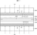
その後、図31に示すように、光熱変換層14にレーザ(LB)を照射することにより、熱膨張層13を非熱膨張層12に対して急激に熱膨張および熱収縮させることによって、熱膨張層13と非熱膨張層12を剥離し、ガラス基板500をTFT基板100あるいは対向基板200から分離する。レーザの照射条件、剥離のメカニズム等は実施例1で説明したのと同様である。
図29に戻り、液晶表示装置が有機EL表示装置と異なる点はバックライトを用いているという点である。積層膜の内、接着層11と熱膨張層12については、実施例3で説明したとおりである。図29では、さらに、バリア層としてのSiO層15及びバリア層としてのAlO層16が形成されている。SiO層は、図26に示すように、可視光の透過率には殆ど影響がない。また、AlO層も、可視光領域では、界面における反射を含めても透過率は90%であり、透過率への影響は殆ど無視することが出来る。このように、実施例4における液晶表示装置においても、実施例3の場合と同様、接着層11の金属材料に注意すれば、本発明は問題なく適用することが出来る。
図32は、本明細書に関連する材料の熱特性をまとめた表である。図32において、熱膨張層13として用いる材料としてのAlと非熱膨張層12の材料として用いるSiOの組み合わせは、本発明にとって非常に優れた効果を持つことがわかる。
実施例1乃至4では、光熱変換層14はa-Siであるとして説明した。しかし、図11に記載のように、波長が308nm、355nmの紫外線レーザに対してはpoly-Siも100%吸収する。したがって、poly-Siを光熱変換層として用いることも出来る。
また、接着層11の例として、Al、Cr,Tiを挙げたが、例えば、金属酸化物である、アルミニウム酸化物AlOを使用しても接着力を上げることが出来る。すなわち、図10に示すように、接着層11にAlOOHが存在すれば、このOH基が脱水和反応によって、ポリイミド中のアミド基とカルボシキル基と結合し、ポリイミドとAlOとの強固な結合を構成できるからである。
さらに、AlOは可視光に対して透明であるため、本発明を液晶表示装置に適用する場合に大きなメリットがある。すなわち、AlOを用いれば、液晶表示装置においても、接着層11の厚さを選択する自由度を大きくとることが出来る。その他、透明導電膜ITOも表面にOH基が存在し、可視光に対し透明のため、AlOと同様に適用できる。
11…接着層、 12…非熱膨張層、 13…熱膨張層、 14…光熱変換層、15…SiOバリア層、16…AlOバリア層、 20…多層膜、 21…多層膜、 80…走査線駆動回路、 90…表示領域、 91…走査線、 92…映像信号線、 93…電源線、 95…画素、 100…TFT基板、 101…TFT回路層、 102…保護層、 103…円偏光板、 111…溶融層、 112…気化した領域、 113…再凝固層、 120…下偏光板、 150…シール材、 200…対向基板、 201…カラーフィルタ層、 220…上偏光板、 300…液晶、 400…フレキシブル配線基板、 500…ガラス基板、 600…バックライト、 LB…レーザビーム
Claims (20)
- 樹脂基板上に画素が形成された表示装置であって、
前記樹脂基板の前記画素が形成された側とは逆側の面に金属または金属酸化物からなる第1の層が形成され、
前記第1の層の前記樹脂基板に対向する面と反対側の面に接して第1の絶縁物からなる第2の層が形成されていることを特徴とする表示装置。 - 前記樹脂基板はポリイミドで形成されていることを特徴とする請求項1に記載の表示装置。
- 前記第1の層はAlで形成されていることを特徴とする請求項1に記載の表示装置。
- 前記Alの層は10nm以下であることを特徴とする請求項3に記載の表示装置。
- 前記第1の層はアルミニウム酸化膜で形成されていることを特徴とする請求項1に記載の表示装置。
- 前記第2の層は酸化シリコンで形成されていることを特徴とする請求項1に記載の表示装置。
- 前記第2の層は、50乃至200nmであることを特徴とする請求項1に記載の表示装置。
- 前記第2の層は前記第1の層よりも膜厚が大きいことを特徴とする請求項1に記載の表示装置。
- 前記第2の層の前記樹脂基板に対向する面と反対側の面に接して第2の絶縁物からなる第3の層が形成され、前記第3の層の前記樹脂基板に対向する面と反対側の面に接して第3の絶縁物からなる第4の層が形成されていることを特徴とする請求項1に記載の表示装置。
- 前記第3の層は、アルミニウム酸化物で形成され、前記第4の層はシリコン酸化物で形成されていることを特徴とする請求項1に記載の表示装置。
- 前記第1の層は、前記第4の層よりも薄いことを特徴とする請求項9に記載の表示装置。
- 樹脂基板上に画素が形成された表示装置の製造方法であって、
ガラス基板上に半導体で形成される第1の層を形成し、
前記第1の層の上に第1の金属からなる第2の層を形成し、
前記第2の層の上に第1の絶縁物からなる第3の層を形成し、
前記第3の層の上に、第2の金属または金属酸化物からなる第4の層を形成し、
前記第4の層の上に、ポリイミドの前駆体を塗布し、焼成して、ポリイミド基板を形成し、
前記ポリイミド基板の上に前記画素を形成し、
その後、前記第1の層にレーザを照射することにより、前記第2の層と前記第3の層間で剥離を生じさせることによって、前記ポリイミド基板と前記ガラス基板を分離することを特徴とする表示装置の製造方法。 - 前記第1の層はa-Siで形成することを特徴とする請求項12に記載の表示装置の製造方法。
- 前記第2の層は、Alで形成することを特徴とする請求項12に記載の表示装置の製造方法。
- 前記第3の層はシリコン酸化膜で形成することを特徴とする請求項12に記載の表示装置の製造方法。
- 前記第4の層はAlで形成することを特徴とする請求項12に記載の表示装置の製造方法。
- 前記第3の層は、前記第2の層よりも膜厚を大きく形成することを特徴とする請求項12に記載の表示装置の製造方法。
- 樹脂基板上に画素が形成された表示装置の製造方法であって、
ガラス基板上に半導体で形成される第1の層を形成し、
前記第1の層の上に第1の金属からなる第2の層を形成し、
前記第2の層の上に第1の絶縁物からなる第3の層を形成し、
前記第3の層の上に、第2の絶縁物からなる第4の層を形成し、
前記第4の層の上に第3の絶縁物からなる第5の層を形成し、
前記第5の層の上に第2の金属、または、金属酸化物からなる第6の層を形成し、
前記第6の層の上に、ポリイミドの前駆体を塗布し、焼成して、ポリイミド基板を形成し、
前記ポリイミド基板の上に前記画素を形成し、
その後、前記第1の層にレーザを照射することにより、前記第2の層と前記第3の層間で剥離を生じさせることによって、前記ポリイミド基板と前記ガラス基板を分離することを特徴とする表示装置の製造方法。 - 前記第1の層はa-Siで形成し、前記第2の層はAlで形成し、前記第3の層は酸化シリコンで形成することを特徴とする請求項18に記載の表示装置の製造方法。
- 前記第4の層はアルミニウム酸化物で形成し、前記第5の層はシリコン酸化物で形成し、前記第6の層は、Alまたはアルミニウム酸化物で形成することを特徴とする請求項18に記載の表示装置の製造方法。
Priority Applications (1)
| Application Number | Priority Date | Filing Date | Title |
|---|---|---|---|
| US16/910,084 US11616104B2 (en) | 2017-12-27 | 2020-06-24 | Display device and method for producing same |
Applications Claiming Priority (2)
| Application Number | Priority Date | Filing Date | Title |
|---|---|---|---|
| JP2017-251073 | 2017-12-27 | ||
| JP2017251073A JP2019117291A (ja) | 2017-12-27 | 2017-12-27 | 表示装置及びその製造方法 |
Related Child Applications (1)
| Application Number | Title | Priority Date | Filing Date |
|---|---|---|---|
| US16/910,084 Continuation US11616104B2 (en) | 2017-12-27 | 2020-06-24 | Display device and method for producing same |
Publications (1)
| Publication Number | Publication Date |
|---|---|
| WO2019130649A1 true WO2019130649A1 (ja) | 2019-07-04 |
Family
ID=67063314
Family Applications (1)
| Application Number | Title | Priority Date | Filing Date |
|---|---|---|---|
| PCT/JP2018/031124 Ceased WO2019130649A1 (ja) | 2017-12-27 | 2018-08-23 | 表示装置及びその製造方法 |
Country Status (3)
| Country | Link |
|---|---|
| US (1) | US11616104B2 (ja) |
| JP (1) | JP2019117291A (ja) |
| WO (1) | WO2019130649A1 (ja) |
Families Citing this family (3)
| Publication number | Priority date | Publication date | Assignee | Title |
|---|---|---|---|---|
| US11889741B2 (en) | 2020-11-20 | 2024-01-30 | Samsung Display Co., Ltd. | Display panel and method of manufacturing the same |
| JP7721082B2 (ja) * | 2021-09-03 | 2025-08-12 | 学校法人早稲田大学 | 易解体方法および易解体可能な構造体 |
| TWI862277B (zh) * | 2023-11-14 | 2024-11-11 | 友達光電股份有限公司 | 離型結構及基板的製造方法 |
Citations (5)
| Publication number | Priority date | Publication date | Assignee | Title |
|---|---|---|---|---|
| WO2009037797A1 (ja) * | 2007-09-20 | 2009-03-26 | Sharp Kabushiki Kaisha | 表示装置の製造方法及び積層構造体 |
| US20110059561A1 (en) * | 2009-09-08 | 2011-03-10 | Chimei Innolux Corporation | Method for fabricating a flexible display device |
| JP2011048374A (ja) * | 2009-08-28 | 2011-03-10 | Samsung Mobile Display Co Ltd | フレキシブル(flexible)表示装置及びその製造方法 |
| WO2016168341A1 (en) * | 2015-04-13 | 2016-10-20 | Royole Corporation | Support and detachment of flexible substrates |
| JP2017208254A (ja) * | 2016-05-19 | 2017-11-24 | 株式会社ジャパンディスプレイ | 表示装置及びその製造方法 |
Family Cites Families (7)
| Publication number | Priority date | Publication date | Assignee | Title |
|---|---|---|---|---|
| JP5239630B2 (ja) | 2008-08-26 | 2013-07-17 | 住友金属鉱山株式会社 | 吸収型多層膜ndフィルター |
| JP2013127905A (ja) | 2011-12-19 | 2013-06-27 | Koito Mfg Co Ltd | ランプ装飾部材及び車両用ランプ |
| KR20150043890A (ko) * | 2013-10-15 | 2015-04-23 | 삼성디스플레이 주식회사 | 유기 발광 표시 장치 |
| KR102271659B1 (ko) * | 2014-08-29 | 2021-06-30 | 엘지디스플레이 주식회사 | 터치 패널 내장형 유기 발광 표시 장치 |
| KR102313361B1 (ko) * | 2014-11-17 | 2021-10-18 | 삼성디스플레이 주식회사 | 유기 발광 표시 장치, 이를 포함하는 전자 기기, 및 유기 발광 표시 장치의 제조 방법 |
| JP2017208253A (ja) * | 2016-05-19 | 2017-11-24 | 株式会社ジャパンディスプレイ | 表示装置 |
| JP2017212038A (ja) * | 2016-05-23 | 2017-11-30 | 株式会社ジャパンディスプレイ | 表示装置 |
-
2017
- 2017-12-27 JP JP2017251073A patent/JP2019117291A/ja active Pending
-
2018
- 2018-08-23 WO PCT/JP2018/031124 patent/WO2019130649A1/ja not_active Ceased
-
2020
- 2020-06-24 US US16/910,084 patent/US11616104B2/en active Active
Patent Citations (5)
| Publication number | Priority date | Publication date | Assignee | Title |
|---|---|---|---|---|
| WO2009037797A1 (ja) * | 2007-09-20 | 2009-03-26 | Sharp Kabushiki Kaisha | 表示装置の製造方法及び積層構造体 |
| JP2011048374A (ja) * | 2009-08-28 | 2011-03-10 | Samsung Mobile Display Co Ltd | フレキシブル(flexible)表示装置及びその製造方法 |
| US20110059561A1 (en) * | 2009-09-08 | 2011-03-10 | Chimei Innolux Corporation | Method for fabricating a flexible display device |
| WO2016168341A1 (en) * | 2015-04-13 | 2016-10-20 | Royole Corporation | Support and detachment of flexible substrates |
| JP2017208254A (ja) * | 2016-05-19 | 2017-11-24 | 株式会社ジャパンディスプレイ | 表示装置及びその製造方法 |
Also Published As
| Publication number | Publication date |
|---|---|
| US20200328262A1 (en) | 2020-10-15 |
| JP2019117291A (ja) | 2019-07-18 |
| US11616104B2 (en) | 2023-03-28 |
Similar Documents
| Publication | Publication Date | Title |
|---|---|---|
| US11409145B2 (en) | Display device | |
| CN101653040B (zh) | 电子设备及其制造方法 | |
| US9666832B2 (en) | Display device and method of manufacturing the same | |
| CN100391004C (zh) | 半导体装置以及半导体装置的制作方法 | |
| US9536929B2 (en) | Display device and method of manufacturing the same | |
| JP2015060780A (ja) | 表示装置の製造方法及び製造システム | |
| WO1999001899A1 (en) | Method of transferring thin film devices, thin film device, thin film integrated circuit device, active matrix substrate, liquid crystal display, and electronic apparatus | |
| WO2019130649A1 (ja) | 表示装置及びその製造方法 | |
| JP2017208254A (ja) | 表示装置及びその製造方法 | |
| JP2017211420A (ja) | 表示装置及びその製造方法 | |
| JP2011107432A (ja) | 電気光学装置の製造方法 | |
| JP6446507B2 (ja) | 表示装置の製造方法 | |
| WO2017014136A1 (ja) | デバイス基板、液晶表示装置、及びデバイス基板の製造方法 | |
| CN115101505A (zh) | 一种基板、制备方法及电子装置 | |
| WO2019106935A1 (ja) | 表示装置 | |
| WO2019239982A1 (ja) | 表示装置 | |
| JP2019113601A (ja) | 表示装置 | |
| JP7051446B2 (ja) | 表示装置の製造方法 | |
| JP2005183718A (ja) | 回路基板、電気光学装置及び電子機器 |
Legal Events
| Date | Code | Title | Description |
|---|---|---|---|
| 121 | Ep: the epo has been informed by wipo that ep was designated in this application |
Ref document number: 18893909 Country of ref document: EP Kind code of ref document: A1 |
|
| NENP | Non-entry into the national phase |
Ref country code: DE |
|
| 122 | Ep: pct application non-entry in european phase |
Ref document number: 18893909 Country of ref document: EP Kind code of ref document: A1 |