WO2019116647A1 - 半導体装置及び無線通信装置 - Google Patents
半導体装置及び無線通信装置 Download PDFInfo
- Publication number
- WO2019116647A1 WO2019116647A1 PCT/JP2018/032801 JP2018032801W WO2019116647A1 WO 2019116647 A1 WO2019116647 A1 WO 2019116647A1 JP 2018032801 W JP2018032801 W JP 2018032801W WO 2019116647 A1 WO2019116647 A1 WO 2019116647A1
- Authority
- WO
- WIPO (PCT)
- Prior art keywords
- frequency
- capacitors
- semiconductor device
- signal
- oscillator
- Prior art date
- Legal status (The legal status is an assumption and is not a legal conclusion. Google has not performed a legal analysis and makes no representation as to the accuracy of the status listed.)
- Ceased
Links
Images








Classifications
-
- H—ELECTRICITY
- H03—ELECTRONIC CIRCUITRY
- H03J—TUNING RESONANT CIRCUITS; SELECTING RESONANT CIRCUITS
- H03J5/00—Discontinuous tuning; Selecting predetermined frequencies; Selecting frequency bands with or without continuous tuning in one or more of the bands, e.g. push-button tuning, turret tuner
- H03J5/02—Discontinuous tuning; Selecting predetermined frequencies; Selecting frequency bands with or without continuous tuning in one or more of the bands, e.g. push-button tuning, turret tuner with variable tuning element having a number of predetermined settings and adjustable to a desired one of these settings
- H03J5/0245—Discontinuous tuning using an electrical variable impedance element, e.g. a voltage variable reactive diode, in which no corresponding analogue value either exists or is preset, i.e. the tuning information is only available in a digital form
- H03J5/0254—Discontinuous tuning using an electrical variable impedance element, e.g. a voltage variable reactive diode, in which no corresponding analogue value either exists or is preset, i.e. the tuning information is only available in a digital form the digital values being transfered to a D/A converter
-
- H—ELECTRICITY
- H03—ELECTRONIC CIRCUITRY
- H03B—GENERATION OF OSCILLATIONS, DIRECTLY OR BY FREQUENCY-CHANGING, BY CIRCUITS EMPLOYING ACTIVE ELEMENTS WHICH OPERATE IN A NON-SWITCHING MANNER; GENERATION OF NOISE BY SUCH CIRCUITS
- H03B5/00—Generation of oscillations using amplifier with regenerative feedback from output to input
- H03B5/08—Generation of oscillations using amplifier with regenerative feedback from output to input with frequency-determining element comprising lumped inductance and capacitance
- H03B5/12—Generation of oscillations using amplifier with regenerative feedback from output to input with frequency-determining element comprising lumped inductance and capacitance active element in amplifier being semiconductor device
- H03B5/1206—Generation of oscillations using amplifier with regenerative feedback from output to input with frequency-determining element comprising lumped inductance and capacitance active element in amplifier being semiconductor device using multiple transistors for amplification
- H03B5/1212—Generation of oscillations using amplifier with regenerative feedback from output to input with frequency-determining element comprising lumped inductance and capacitance active element in amplifier being semiconductor device using multiple transistors for amplification the amplifier comprising a pair of transistors, wherein an output terminal of each being connected to an input terminal of the other, e.g. a cross coupled pair
- H03B5/1215—Generation of oscillations using amplifier with regenerative feedback from output to input with frequency-determining element comprising lumped inductance and capacitance active element in amplifier being semiconductor device using multiple transistors for amplification the amplifier comprising a pair of transistors, wherein an output terminal of each being connected to an input terminal of the other, e.g. a cross coupled pair the current source or degeneration circuit being in common to both transistors of the pair, e.g. a cross-coupled long-tailed pair
-
- H—ELECTRICITY
- H03—ELECTRONIC CIRCUITRY
- H03B—GENERATION OF OSCILLATIONS, DIRECTLY OR BY FREQUENCY-CHANGING, BY CIRCUITS EMPLOYING ACTIVE ELEMENTS WHICH OPERATE IN A NON-SWITCHING MANNER; GENERATION OF NOISE BY SUCH CIRCUITS
- H03B5/00—Generation of oscillations using amplifier with regenerative feedback from output to input
- H03B5/08—Generation of oscillations using amplifier with regenerative feedback from output to input with frequency-determining element comprising lumped inductance and capacitance
- H03B5/12—Generation of oscillations using amplifier with regenerative feedback from output to input with frequency-determining element comprising lumped inductance and capacitance active element in amplifier being semiconductor device
- H03B5/1228—Generation of oscillations using amplifier with regenerative feedback from output to input with frequency-determining element comprising lumped inductance and capacitance active element in amplifier being semiconductor device the amplifier comprising one or more field effect transistors
-
- H—ELECTRICITY
- H03—ELECTRONIC CIRCUITRY
- H03B—GENERATION OF OSCILLATIONS, DIRECTLY OR BY FREQUENCY-CHANGING, BY CIRCUITS EMPLOYING ACTIVE ELEMENTS WHICH OPERATE IN A NON-SWITCHING MANNER; GENERATION OF NOISE BY SUCH CIRCUITS
- H03B5/00—Generation of oscillations using amplifier with regenerative feedback from output to input
- H03B5/08—Generation of oscillations using amplifier with regenerative feedback from output to input with frequency-determining element comprising lumped inductance and capacitance
- H03B5/12—Generation of oscillations using amplifier with regenerative feedback from output to input with frequency-determining element comprising lumped inductance and capacitance active element in amplifier being semiconductor device
- H03B5/1237—Generation of oscillations using amplifier with regenerative feedback from output to input with frequency-determining element comprising lumped inductance and capacitance active element in amplifier being semiconductor device comprising means for varying the frequency of the generator
- H03B5/1262—Generation of oscillations using amplifier with regenerative feedback from output to input with frequency-determining element comprising lumped inductance and capacitance active element in amplifier being semiconductor device comprising means for varying the frequency of the generator the means comprising switched elements
- H03B5/1265—Generation of oscillations using amplifier with regenerative feedback from output to input with frequency-determining element comprising lumped inductance and capacitance active element in amplifier being semiconductor device comprising means for varying the frequency of the generator the means comprising switched elements switched capacitors
-
- H—ELECTRICITY
- H03—ELECTRONIC CIRCUITRY
- H03L—AUTOMATIC CONTROL, STARTING, SYNCHRONISATION OR STABILISATION OF GENERATORS OF ELECTRONIC OSCILLATIONS OR PULSES
- H03L7/00—Automatic control of frequency or phase; Synchronisation
- H03L7/06—Automatic control of frequency or phase; Synchronisation using a reference signal applied to a frequency- or phase-locked loop
- H03L7/08—Details of the phase-locked loop
- H03L7/099—Details of the phase-locked loop concerning mainly the controlled oscillator of the loop
- H03L7/0991—Details of the phase-locked loop concerning mainly the controlled oscillator of the loop the oscillator being a digital oscillator, e.g. composed of a fixed oscillator followed by a variable frequency divider
- H03L7/0992—Details of the phase-locked loop concerning mainly the controlled oscillator of the loop the oscillator being a digital oscillator, e.g. composed of a fixed oscillator followed by a variable frequency divider comprising a counter or a frequency divider
-
- H—ELECTRICITY
- H03—ELECTRONIC CIRCUITRY
- H03J—TUNING RESONANT CIRCUITS; SELECTING RESONANT CIRCUITS
- H03J2200/00—Indexing scheme relating to tuning resonant circuits and selecting resonant circuits
- H03J2200/10—Tuning of a resonator by means of digitally controlled capacitor bank
Definitions
- the present disclosure relates to a semiconductor device and a wireless communication device.
- a high frequency radio signal is amplified by an RF (Radio Frequency) amplifier, and the amplified radio signal is converted by a mixer circuit into an IF (Intermediate Frequency) signal having a low frequency, and the converted IF signal is used.
- a voice signal can be obtained by demodulation with a demodulator.
- a local oscillation signal having a frequency corresponding to the sum of the input frequency of the radio signal and the frequency of the IF signal is multiplied by the radio signal.
- the radio receiver may be provided with a PLL (Phase Locked Loop) synthesizer for controlling the frequency of the local oscillation signal.
- the PLL synthesizer performs feedback to match the phase of a signal from a crystal oscillator that oscillates a signal having a fixed frequency, thereby accurately and stably a local oscillation signal having a desired frequency. Can be obtained.
- the radio receiver not only can obtain a local oscillation signal having a desired frequency accurately and stably by using a PLL synthesizer, but it is possible to use different frequencies with only one crystal oscillator.
- a plurality of types of local oscillation signals can be obtained. For example, as a circuit configuration using a PLL synthesizer, the following Patent Document 1 can be mentioned.
- the radio receiver when the PLL synthesizer as described above is provided, various circuit blocks and parts such as a phase comparator are required, which increases the manufacturing cost and further the power consumption. It will cause an increase. Therefore, there is a radio receiver provided with a variable capacitor instead of the PLL synthesizer as described above in order to suppress an increase in manufacturing cost and power consumption.
- the variable capacitor is a mechanical component whose capacitance value can be changed manually by the user. Therefore, in the radio receiver, by providing the variable capacitor in the oscillator that generates the local oscillation signal, the frequency of the local oscillation signal can be changed linearly and continuously according to the change in capacitance. Can. Although the radio receiver using such variable capacitors is inferior in accuracy of control of the frequency of the local oscillation signal to the case of using a PLL synthesizer, it is possible to suppress an increase in manufacturing cost and power consumption.
- Patent No. 5668082 gazette
- variable capacitors have decreased, and as a result, the price of variable capacitors tends to increase. Therefore, in the radio receiver, it has become difficult to reduce the manufacturing cost and the power consumption while maintaining the manual operability of the user at the time of radio broadcast tuning. Under these circumstances, there is a need for a semiconductor device provided with a new oscillation circuit (oscillator) to be mounted on a radio receiver in order to reduce manufacturing costs and power consumption while maintaining manual operability.
- oscillation circuit oscillation circuit
- the present disclosure proposes a new and improved semiconductor device and wireless communication device capable of reducing manufacturing cost and power consumption while maintaining manual operability.
- an oscillation circuit including a plurality of capacitors provided on a semiconductor substrate, a conversion circuit that converts an analog signal into a digital signal, and a switch circuit that switches the capacitor based on the digital signal are included.
- a semiconductor device is provided, in which an oscillation frequency changes linearly with a change in the analog signal.
- an oscillation circuit including a plurality of capacitors provided on a semiconductor substrate, a conversion circuit that converts an analog signal into a digital signal, and a switch circuit that switches the capacitor based on the digital signal.
- a wireless communication apparatus mounted with a semiconductor device, wherein the oscillation frequency changes linearly with respect to the change of the analog signal.
- FIG. 2 is a circuit diagram schematically showing a configuration of a capacitor bank 100 according to the same embodiment. It is a graph which shows an example of a change of oscillation frequency of oscillator 10 concerning the embodiment. It is an explanatory view (the 1) for explaining the control method of the frequency concerning a 2nd embodiment of this indication. It is an explanatory view (the 2) for explaining the control method of the frequency concerning the embodiment. It is an explanatory view (the 3) for explaining the control method of the frequency concerning the embodiment.
- FIG. 14 is a layout view schematically showing a configuration example of a capacitor 102 according to a fourth embodiment of the present disclosure.
- FIG. 2 is a layout view schematically showing a configuration example of an oscillator 10 according to the same embodiment. It is a circuit diagram showing roughly the composition of radio receiver 60 concerning a 5th embodiment of this indication.
- FIG. 16 is a circuit diagram schematically showing a configuration of a local oscillation signal generation unit 70 according to a sixth embodiment of the present disclosure. It is an explanatory view for explaining division in a local oscillation signal generation unit 70 according to the embodiment. It is a graph (the 1) which shows an example of change of the frequency of local oscillation signal generation part 70 concerning the embodiment.
- a plurality of components having substantially the same or similar functional configurations may be distinguished by attaching different numerals after the same reference numerals. However, when it is not necessary to distinguish each of a plurality of components having substantially the same or similar functional configuration, only the same reference numeral is given. Also, similar components in different embodiments may be distinguished by attaching different alphabets after the same reference numerals. However, when it is not necessary to distinguish each of similar components in particular, only the same reference numeral is attached.
- connection means to electrically connect a plurality of elements unless otherwise noted. Furthermore, in the following description, “connection” is not only directly and electrically connecting a plurality of elements, but also indirectly and electrically through other elements. Also includes. Furthermore, in the following description, “connect in series” means to connect a plurality of elements in a row, and “connect in parallel” means to connect two terminals of each element. It means connecting with each other. For example, when there are two elements having an A terminal and a B terminal, when the B terminal of one element and the A terminal of the other element are connected, it is called a state of being connected in series. When the A terminals of the elements are connected to each other and the B terminals are connected to each other, it is referred to as being connected in parallel.
- a layout diagram referred to in the following description is a diagram for explaining an embodiment of the present disclosure and a diagram for promoting the understanding thereof, and for the sake of clarity, the shapes, sizes, ratios, etc. shown in the drawings are It may be different from the actual. Further, the shapes and the like of the respective elements shown in the drawings can be appropriately changed in design in consideration of the following description and known techniques.
- the embodiments of the present disclosure described below relate to an oscillator that can be used for a radio receiver, a local oscillation signal generation unit having an oscillator, and a radio receiver having these.
- the oscillator according to the embodiments of the present disclosure described below is not limited to use in a radio receiver, and can be used in various wireless communication devices.
- FIG. 22 to FIG. 22 and 23 are circuit diagrams schematically showing configuration examples of the radio receivers 60a and 60b according to the comparative example.
- FIG. 24 is a graph showing an example of the change in capacitance value with respect to the rotation angle of the variable capacitor 602.
- the comparative example means a radio receiver, a variable capacitor, and the like which have been studied until the present inventors create an embodiment according to the present disclosure.
- a radio signal which is a high frequency modulated with AM (Amplitude Modulation) or FM (Frequency Modulation) is amplified by the RF amplifier 702, and the amplified radio signal is amplified.
- the mixer circuit 704 converts it into an IF signal having a low frequency.
- an unnecessary signal is removed by the band pass filter 718, and the converted IF signal is amplified by the IF amplifier 720 and then demodulated by the demodulator 722 to obtain an audio signal. it can.
- frequency conversion for converting a high-frequency radio signal into an IF signal is performed by the mixer circuit 704.
- the local oscillation signal has a frequency corresponding to the sum of the input frequency of the radio signal and the frequency of the IF signal. This can be done by multiplying the signal with the radio signal.
- the local oscillation signal is required to have a wide band frequency in order to cover the entire band possessed by the radio signal, so that the oscillator 90a generating the local oscillation signal can largely change the frequency of the oscillation signal.
- an oscillator 90a a configuration in which an inductor 300, a variable capacitance 502, and a negative resistance circuit 40 are connected in parallel as shown in FIG. 23 can be mentioned.
- the frequency F of the oscillation signal generated by the oscillator 90a is expressed by the following equation (1). Can.
- the oscillator 90a can largely change the frequency of the oscillation signal, so that the local oscillation signal has a wide band frequency covering the entire band of the radio signal. be able to.
- the radio receiver 60a changes the frequency of the oscillation signal of the oscillator 90a as described above to tune to the frequency of the radio signal of the desired radio station, thereby broadcasting the desired radio station. It can be tuned. At this time, the radio receiver 60a can not perform tuning properly unless it is precisely tuned to the frequency of the radio signal associated with the desired radio station. Therefore, in the radio receiver 60a, it is required to accurately change the frequency of the local oscillation signal.
- the radio receiver 60a in the comparative example has a voltage controlled oscillator 90a including a variable capacitance 502 whose capacitance value changes according to the input voltage. Furthermore, the radio receiver 60a has a PLL synthesizer 716 that controls the frequency of the oscillation signal with high accuracy by using the accuracy of the frequency of the reference signal generated by the crystal oscillator 706.
- the PLL synthesizer 716 includes a phase comparator 708, a frequency divider 710, a charge pump 712, a loop filter 714, and the like in addition to the oscillator 90a.
- the PLL synthesizer 716 inputs the signal from the crystal oscillator 706 that oscillates a signal having a fixed frequency and the signal obtained by dividing the oscillation signal from the oscillator 90a to the phase comparator 708 and compares the phases of each other. , Feedback to the oscillator 90a to bring the phases into phase. By doing this, the radio receiver 60a can accurately and stably obtain an oscillation signal having a desired frequency. Further, in the radio receiver 60a, the frequency of the oscillation signal can be changed by changing the division number by the frequency divider 710, and the oscillation signal has a wide band covering the entire band of the radio signal. It can have a frequency. Therefore, the frequency of the oscillation signal generated by the oscillator 90a is set to be an integral multiple of the frequency of the reference signal transmitted by the crystal oscillator 706.
- the crystal oscillator 706 when the PLL synthesizer 716 is provided in the radio receiver 60a, the crystal oscillator 706 generates a reference signal in addition to the voltage controlled oscillator 90a whose frequency changes according to the input voltage, A phase comparator 708, a frequency divider 710, a charge pump 712, and a loop filter 714 are required. Furthermore, in the radio receiver 60a, a microcomputer for control (not shown), a display unit with liquid crystal (not shown), etc. are also required. Therefore, the radio receiver 60a according to the comparative example shown in FIG. 22 can accurately and stably obtain an oscillation signal having a desired frequency, but various circuit blocks are required. The manufacturing cost is increased and the power consumption is increased.
- the above-described PLL synthesizer 716 is not used in a low-power radio receiver 60b that is inexpensive and requires long-time operation using dry batteries or the like, such as an emergency radio receiver used in a disaster. There is something. More specifically, as shown in FIG. 23, in the radio receiver 60b, instead of using the PLL synthesizer 716, the oscillator 90b can be a variable capacitor capable of mechanically changing the capacitance value manually by the user. 602 is included.
- the variable capacitor 602 can change the capacitance value by changing the area in which the electrode pairs face each other. Specifically, as shown in FIG. 24, by rotating one of the electrode pairs of the variable capacitor 602, the electrostatic capacitance value of the variable capacitor 602 can be changed continuously.
- the frequency of the oscillation signal generated by the oscillator 90a with respect to the rotation angle by the user's manual operation. can be varied linearly. Therefore, in the radio receiver 60b, the frequency of the oscillation signal can be changed linearly, continuously, and with a small change width according to the user's manual operation.
- the radio receiver 60b is inferior in accuracy of control of the frequency of the oscillation signal as compared with the case of using the PLL synthesizer 716, the user's manual direct operation is possible at the time of radio broadcast channel selection. , The increase in manufacturing cost and power consumption can be suppressed.
- variable capacitors 602 As described above, in recent years, the production volume of variable capacitors 602 has decreased, and as a result, the price of variable capacitors 602 tends to increase. Therefore, in the radio receiver 60b that is required to be inexpensive and consumes low power, it has been desired to replace the variable capacitor 602 with another component. As other parts to be replaced, various parts can be assumed, but in order to further suppress an increase in manufacturing cost, to be formed on a semiconductor chip (semiconductor device) like other circuit blocks of the radio receiver 60b It is more preferable if it is a component that can
- the present inventors continuously and linearly set the frequency of the oscillation signal according to the user's manual operation, like the radio receiver 60b using the variable capacitor 602. Also, the embodiment of the present disclosure has been created that can reduce the manufacturing cost and the power consumption while maintaining the manual operability, which can be changed with a minute change width.
- the embodiment of the present disclosure created by the present inventors is not an mechanical component provided outside the semiconductor chip such as the variable capacitor 602 but an oscillator using a capacitor provided on the semiconductor chip. is there.
- the capacitance value of the capacitor is switched by converting the input voltage for oscillation frequency control, which is an analog signal input from the user, into a digital signal, and the converted digital signal.
- the capacitance value of the capacitor included in the oscillator it is possible to obtain an oscillation signal having a frequency that changes linearly, continuously, and with a small change width with respect to the input voltage.
- the manufacturing cost and the power consumption can be suppressed while maintaining the manual operability.
- FIG. 1 is a circuit diagram schematically showing a configuration of an oscillator 10 according to a first embodiment of the present disclosure
- FIG. 2 is a circuit schematically showing a configuration of an oscillator 10a according to a modification of the present embodiment.
- the oscillator 10 is an LC oscillator (oscillation (oscillation) including a capacitor bank (capacitor) 100 including a plurality of capacitors (small capacitors) 102 (see FIG. 3) and an inductor 300.
- a circuit) 20 an AD converter (Analog Digital Converter) (conversion circuit) (referred to as "ADC" in the drawing) 30, a negative resistance circuit 40, and a constant current source 50 are included.
- the oscillator 10 is an oscillator that oscillates an oscillation signal having a predetermined frequency, and the frequency of the oscillation signal linearly, continuously, and minutely changes according to the analog signal input to the AD converter 30. Change in width.
- the oscillator 10 can be formed on one semiconductor substrate as described later.
- the capacitor bank 100 and the inductor 300 are connected in parallel.
- the frequency F of the signal to be oscillated is expressed by the following equation (2) .
- the frequency of the oscillation signal can be changed by changing the total capacitance value of the capacitor bank 100.
- a plurality of capacitance banks 100 connected in parallel may be provided, and the total capacitance value of the plurality of capacitance banks 100 (a plurality of capacitors included in the capacitance bank 100) The sum of capacitance values of 102) may be the same as or different from each other. Further, details of the capacitor bank 100 according to the present embodiment will be described later.
- the negative resistance circuit 40 is connected in parallel to the LC oscillator 20.
- the negative resistance circuit 40 is configured by an NMOS cross couple in which two n-type MOS (Metal Oxide Semiconductor) transistors 400 are connected in cross.
- the configuration of the negative resistance circuit 40 is not particularly limited, and may be a complementary metal oxide semiconductor (CMOS) circuit as shown in FIG.
- CMOS complementary metal oxide semiconductor
- the constant current source 50 is connected to the negative resistance circuit, may be composed of various known constant current source circuits, and may be replaced with a resistor.
- the AD converter 30 is a conversion circuit which is connected to the switch 202 (see FIG. 3) for switching the capacitance value of the capacitor bank 100 and converts the input analog signal into a digital signal. Therefore, the digital signal converted by the AD converter 30 can switch on / off of a plurality of switches (switch circuits) 202 respectively connected to the capacitors 102 of the capacitor bank 100. Such switching makes it possible to change the capacitance The capacitance value of the bank 100 can be varied. Furthermore, in order to ensure the same operability as the radio receiver 60b using the variable capacitor 602 described above, the analog signal input to the AD converter 30 is a variable resistor 80 whose resistance value is changed according to the input from the user. It can be the obtained DC voltage.
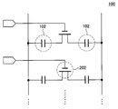
- FIG. 3 is a circuit diagram schematically showing the configuration of the capacitor bank 100 according to the present embodiment.
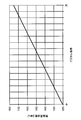
- FIG. 4 is a graph showing an example of the change of the oscillation frequency of the oscillator 10 according to the present embodiment.
- the capacitor bank 100 includes a capacitor having a fixed capacitance value (specifically, a metal insulator metal (MIM) capacitor, a metal oxide metal (MOM) capacitor, etc.) 102. And a switch 202 composed of a MOS transistor. More specifically, one switch 202 and two capacitors 102 connected in series on both sides of the switch 202 constitute one unit, and a plurality of such units are connected in parallel to form the capacitor bank. 100 is configured. By switching the voltage value applied to the gate of the MOS transistor which is the switch 202 of each unit according to the above-mentioned digital signal, the switch 202 is turned on / off, and the total capacitance value of the capacitor bank 100 is discretely It can be switched. Therefore, in the LC oscillator 20 including the capacitor bank 100, the total capacitance value of the capacitor bank 100 is discretely changed by the digital signal, so that the frequency of the oscillation signal is discretely changed.
- a fixed capacitance value specifically, a metal insulator metal (MIM
- the capacitance value and the number of the capacitors 102 constituting the capacitance bank 100 are appropriately selected (for example, the capacitance bank 100 is discretely dispersed with a minute change width by the switch 202).
- the capacitance value of the capacitor 102 of each unit is changed so that the total capacitance value of V) changes linearly and continuously for the input digital signal as shown in FIG. Can generate an oscillation signal whose oscillation frequency changes.
- the digital signal is obtained by converting the analog signal by the AD converter 30, and the analog signal is a variable resistor whose resistance value is changed according to the input from the user.
- 80 is a DC voltage obtained by Therefore, in the oscillator 10 according to the present embodiment, the frequency of the oscillation signal can be changed linearly and continuously according to the user's manual operation. Therefore, the variable capacitor 602 according to the comparative example described above can be obtained. The same operability as the radio receiver 60b using the above can be secured.
- the input digital signal is selected by appropriately selecting the capacitance value and the number of the capacitors 102 that configure the capacitor bank 100. It is possible to generate an oscillation signal in which the oscillation frequency changes linearly and continuously. However, in the first embodiment, the frequency of the oscillation signal is changed by discretely switching the total capacitance value of the capacitor bank 100 by the digital signal. Therefore, in practice, if the total capacitance value of the capacitor bank 100 is not switched with a small change width in the oscillator 10, linear and continuous for a digital signal as shown in FIG. Can not generate an oscillation signal whose oscillation frequency changes.
- the minimum capacity value and the capacity value of the manufacturable capacitor 102 are limited by the semiconductor manufacturing process for manufacturing the capacitor 102, and the total capacity value of the capacity bank 100 may be switched with a minute change width. It may be difficult to obtain multiple capacitors 102, each having possible and desired capacitance values. Therefore, in the second embodiment of the present disclosure described below, it is possible to generate an oscillation signal whose oscillation frequency changes linearly, continuously, and with a minute change width with respect to a digital signal. A method of controlling the frequency of the oscillator 10 is proposed.
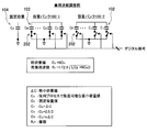
- FIG. 25 is an explanatory diagram for describing a frequency control method according to a comparative example.
- the comparative example means an oscillator and a method of controlling a frequency of the oscillator, which the present inventors have been studying until the embodiment according to the present disclosure is created.
- each capacitor 102 of the capacitor bank 900 has a minimum capacitance value (Cu) that can be manufactured by the semiconductor manufacturing process used.
- the oscillator according to such a comparative example it is considered to change the frequency of the oscillation signal.
- the oscillator according to the comparative example generates an oscillation signal using the fixed capacitance 104 and N capacitors 102 in the capacitance bank 900. It shall be.
- the oscillation frequency F 0 according to the oscillator is represented by the following equation (3).
- the switch 202 of one capacitor 102 in the capacitance bank 900 is turned on, and the oscillator includes the fixed capacitance 104 and the capacitance An oscillation signal is generated using N + 1 capacitors 102 in the bank 900.
- the oscillation frequency F 1 according to the oscillator is represented by the following equation (4).
- the difference between the frequency of the oscillation frequency F 0 and the frequency of the oscillation frequency F 1 is the minimum difference of the oscillation frequency adjustable by the oscillator.
- the capacitance value Cu of each capacitor of the capacitor bank 900 corresponds to the minimum capacitance value that can be manufactured by the semiconductor manufacturing process used, and the value is limited by the semiconductor manufacturing process used. Therefore, in the oscillator according to the comparative example, the frequency change width is larger than the desired frequency change width, and an oscillation signal whose oscillation frequency changes in discrete steps is generated for the digital signal in discrete steps. It will be. In other words, in the oscillator according to the comparative example, it is difficult to generate an oscillation signal whose oscillation frequency changes linearly, continuously, and with a small change width with respect to a digital signal.
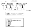
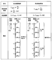
- FIG. 5 to FIG. 7 are explanatory diagrams for describing a frequency control method according to the second embodiment of the present disclosure.
- FIG. 8 is an explanatory view for explaining an example of a change in capacitance value in the frequency control method according to the present embodiment, and FIG.
- FIGS. 5 to 7 the capacitor bank 100 according to the present embodiment is illustrated as being composed of a plurality of capacitors 102 connected in parallel, but the present embodiment is limited to this. Instead, each capacitor 102 shown in the figure may be made up of two capacitors 102 connected in series.
- a plurality of capacitors connected in parallel with a fixed capacitance (capacitance value C 0 ) 104 that can not change the capacitance value is provided.
- 102 capacitor value Cu
- a capacitance bank 100-1 whose capacitance value can be switched by the switch 202, and a plurality of capacitance values different from each other
- a capacitor bank 100-2 having capacitors 102 (electrostatic capacitance values C 1 , C 2 ,..., Cn) and capable of switching the capacitance value by the switch 202 is provided.
- the fixed capacitance 104, the capacitance bank 100-1, and the capacitance bank 100-2 are connected in parallel.
- the fixed capacitor 104 is provided in the oscillator 10 to generate an oscillation signal having a frequency near a desired frequency.
- capacitor bank 100-1 has N capacitors 102, and similar to capacitor bank 900 of the comparative example, the capacitance Cu of each capacitor 102 is the minimum capacitance that can be manufactured by the semiconductor manufacturing process used. It shall have a value (Cu).
- the capacity bank 100-2 has N capacitors 102, and the capacities of the capacitors 102 are different from each other, and are set to the minimum capacity value (minimum unit capacity) (Cu) that can be manufactured by the semiconductor manufacturing process used. It is assumed that the capacitance value has a value obtained by adding an integral multiple of a minute capacitance value (minute capacitance) ( ⁇ C). The minute capacitance value ⁇ C is smaller than the minimum capacitance value Cu.
- the capacitance value Cn of each capacitor 102 included in the capacitance bank 100-2 is expressed by the following equation (5). Specifically, the capacitance value C of the first capacitor (second small capacitor) is 1 is Cu + ⁇ C, and the capacitance value C 2 of the second capacitor (third small capacitor) is Cu + 2 ⁇ C.
- the minimum capacitance value Cu is about several 10 fF
- the small capacitance value ⁇ C is about several fF.
- one oscillator 10 may have two or more capacity banks 100 connected in parallel, and furthermore, the total capacity value of each capacity bank 100 can be different from each other.
- the minimum capacitance value and the minute amount value may be different for each capacitance bank 100, and the minimum capacitance value is not limited to the minimum capacitance value that can be manufactured by the semiconductor manufacturing process.
- the oscillator 10 according to the present embodiment can have about 10 to 20 capacitor banks 100, and each capacitor bank 100 can have about several capacitors 102.
- control of the frequency of the oscillator 10 generates an oscillation signal whose oscillation frequency changes linearly, continuously, and with a minute change width to a digital signal.
- the method is as follows.
- the oscillation frequency F 1 ′ is expressed by the following equation (7).
- one capacitor 102 of the capacitor bank 100-1 in the oscillator 10 is turned off. Since the total capacitance value in the oscillator 10 is C 0 + (N ⁇ 1) Cu + (Cu + ⁇ C), that is, C 0 + NCu + ⁇ C, the oscillation frequency F 1 is expressed by the following equation (8).
- the oscillator 10 As shown in FIG. 8, the oscillator 10 according to this embodiment, the total capacitance value of the post-frequency adjustment before the frequency adjustment, since it is changed to C 0 + NCu + ⁇ C from C 0 + NCU, minute capacitance value [Delta] C It can be seen that the change width (step width) of On the other hand, in the comparative example described above, the total capacitance value of the post-frequency adjustment before the frequency adjustment, since it is changed to C 0 + (N + 1) Cu from C 0 + NCU, the change in the minimum capacitance value Cu It is changing in width.
- the change of the total capacitance value as described above brings about the change of the oscillation frequency as shown in FIG.
- the oscillation frequencies before and after the frequency adjustment change from F 0 to F 1 and the oscillation frequency F 0 and the oscillation frequency
- the minute frequency change width ⁇ F corresponds to the minute capacitance value ⁇ C.
- the oscillation frequency and after frequency adjustment before the frequency adjustment is changed from F 0 to F 0 -Fu, the oscillation frequency is changed by the change width Fu corresponding to the minimum capacitance value Cu doing. Since the minute capacitance value ⁇ C is smaller than the minimum capacitance value Cu, the minute frequency change width ⁇ F according to the present embodiment is smaller than the change width Fu according to the comparative example.
- the frequency control method even if there is a limitation on the minimum capacity value that can be manufactured by the semiconductor manufacturing process used, it is possible to have a minute frequency change width ⁇ F. As a result, according to the present embodiment, it is possible to generate an oscillation signal whose oscillation frequency changes linearly, continuously, and with a minute change width with respect to a digital signal.
- the method of controlling the frequency is not limited to those shown in FIGS. 5 to 7 and, for example, the oscillator 10 is controlled to be in the state of FIG. 7 directly from FIG. You may control.
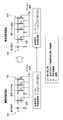
- FIG. 10 is an explanatory diagram for describing a frequency control method according to the present embodiment.
- FIG. 11 is an explanatory view for explaining an example of a change in capacitance value in the frequency control method according to the present embodiment
- FIG. 12 is an example of a change in oscillation frequency in the frequency control method according to the present embodiment. It is explanatory drawing explaining.
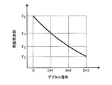
- the total capacitance value corresponds to the change width (step width) of the small capacitance value ⁇ C according to the change of the digital signal to D, D + 1, D + 2 and D + 3. To change.
- the change of the total capacitance value as described above brings about the change of the oscillation frequency as shown in FIG.
- the oscillation frequency is F 0 , F 1 , F 2 according to the change of the digital signal into D, D + 1, D + 2 and D + 3.
- And F 3 changes. Therefore, in the present embodiment, by appropriately selecting the small capacitance value ⁇ C of the capacitors 102 constituting the capacitance bank 100 and the total capacitance value of each capacitance bank 100, the input digital signal is linear.
- the oscillation frequency can be changed continuously and with a small change width.
- the oscillators 10 have different total capacitance values in order to change the oscillation frequency linearly, continuously, and with a small change width with respect to the input digital signal.
- the plurality of different capacity banks 100 may be included. Furthermore, by setting the plurality of capacitor banks 100 to have the total capacitance value (Cn) which increases nonlinearly stepwise in a stepwise manner, the oscillation frequency F of the oscillation frequency shown by the following equation (11) is more linear It is preferable to make it increase.
- the plurality of capacitors 102 included in each capacitor bank 100 have capacitance values different from one another, and specifically, a capacitance value obtained by adding an integral multiple of a small capacitance value ( ⁇ C) to a predetermined capacitance value. It is preferable to have Accordingly, in the same capacitance bank 100, the plurality of capacitors 102 have capacitance values that increase linearly in a stepwise manner.
- the plurality of capacitors 102 are not limited to having capacitance values that increase linearly in a stepwise manner in a stepwise manner. , May have the same capacitance value. However, in the case where the plurality of capacitors 102 have capacitance values that increase linearly in a stepwise manner in a stepwise manner, the increase in the area occupied by the plurality of capacitors 102 on the semiconductor substrate is suppressed, and a wide band and The oscillation frequency can be changed with a minute change width.
- the total capacity value of the oscillator 10 is switched by the binary code (binary system).
- the present invention is not limited to the binary code, and A thermometer code formed by a series of "0" s and a series of "0" s may be used. Further, in the present embodiment, depending on the total capacitance value in the oscillator 10, the binary code may be switched to the thermometer code or vice versa.
- FIG. 13 is a circuit diagram schematically showing a configuration of a capacitor bank 100 a according to a third embodiment of the present disclosure
- FIG. 14 is an explanatory diagram for describing a frequency control method according to the present embodiment. is there.
- a capacitor bank 100a a plurality of capacitors 102 are connected in series.
- the capacitance value Cu of each capacitor 102 corresponds to the minimum capacitance value that can be manufactured by the semiconductor manufacturing process used.
- these capacitors 102 are connected to each other via a switch 202 formed of a MOS transistor.
- the capacitor bank 100 a has a connecting line 204 which runs parallel to the row of the plurality of capacitors 102 connected in series, and each of the connecting lines 204 and each of the capacitors 102 are located between the two capacitors 102.
- the node 206 is connected via the switch 202.
- control of the frequency of the oscillator 10 generates an oscillation signal whose oscillation frequency changes linearly, continuously, and with a minute change width to a digital signal.
- the method is as follows.
- the switch 202 is turned on so that all the M capacitors 102 of the capacitor bank 100 a of the oscillator 10 are connected in series.
- an oscillation signal is generated using the fixed capacitor 104 and the M capacitors 102 connected in series.
- the total capacitance value in the oscillator 10 is expressed by the following equation (12). Note that ⁇ C in the following equation is equal to Cu / M.
- the switch 202 is turned off to disconnect one half of the M capacitors 102 in the capacitor bank 100 a from the series connection.
- an oscillation signal is generated using the fixed capacitance 104 and M / 2 capacitors 102 connected in series.
- the total capacitance value in the oscillator 10 is expressed by the following equation (13).
- the total capacitance value of the oscillator 10 can be obtained by switching the number of capacitors 102 connected in series. Can be changed by a minute change width.
- the number M of series connections of the capacitors 102 in the capacitor bank 100a is increased.
- the number of switches 202 that control the number of series connections also increases. Therefore, in such a case, the area of the semiconductor chip on which the oscillator 10 is provided may be increased, which may increase the manufacturing cost.
- the serial number M of the capacitors 102 can only be set to an integer, the degree of freedom in changing the total capacitance value of the oscillator 10 is low. Therefore, from such a point of view, it is preferable to use the capacitor bank 100 in which a plurality of capacitors 102 are connected in parallel as in the second embodiment described above.
- the digital signal to be input is appropriately selected by appropriately selecting the small capacitance value ⁇ C of the capacitors 102 constituting the capacitor bank 100 and the total capacitance value of each of the capacitor banks 100.
- the oscillation frequency can be changed linearly, continuously, and with a minute change width.
- a capacitor bank 100 is provided on the semiconductor substrate.
- FIGS. 15 and 16 a capacitor bank 100 provided on a semiconductor substrate will be described with reference to FIGS. 15 and 16.
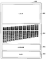
- FIG. 15 is a layout diagram schematically showing a configuration example of the capacitor 102 according to the fourth embodiment of the present disclosure, and FIG.
- FIG. 16 is a layout diagram schematically showing a configuration example of the oscillator 10 according to the present embodiment. It is. In these layout diagrams, in order to make it easy to understand, illustration of wiring, elements and the like is omitted, and only the main part according to the present embodiment is illustrated.
- one capacitor bank 100 has a plurality of capacitors 102 and a plurality of switches 202 formed of MOS transistors arranged on a semiconductor substrate 800. .
- the capacitance values of the plurality of capacitors 102 linearly change in a stepwise manner sequentially along the vertical direction in FIG. 15, and accordingly, the layout areas occupied by the respective capacitors 102 also sequentially linearly change in a stepwise manner. doing.
- seven pairs of capacitor pairs 106 are provided along the vertical direction in the figure, and each capacitor pair 106 has two capacitors 102 having the same capacitance value. They are arranged in line symmetry with the switch 202 in between.
- two capacitors 102 are connected to the switch 202 by a connection line (wiring) 204.
- a plurality of capacitor banks 100 having the configuration as shown in FIG. 15 are formed on the semiconductor substrate 800.
- the oscillator 10 according to the present embodiment has a capacitor bank formation region 804 in which a plurality of capacitor banks 100 are formed on a semiconductor substrate 800.
- an inductor formation region 802 in which the inductor 300 is formed, a negative resistance circuit formation region 806 in which the negative resistance circuit 40 and the like are formed, and the like will be described later It may have a divider formation region 808 or the like in which the divider 710 is formed.
- the plurality of capacity banks 100 may have different total capacity values. Specifically, the plurality of capacity banks 100 have a total capacity value that increases nonlinearly in a stepwise manner in a stepwise manner, and accordingly, the layout area occupied by each capacitive bank 100 also changes in a nonlinear manner in a stepwise manner. There is.
- fixed capacitor 104 may be provided in capacitance bank formation region 804, and a dummy capacitor (not shown) not involved in generation of an oscillation signal is provided in order to form each capacitor 102 with higher accuracy. It may be
- the inductor 300 formed in the inductor forming region 802 may be an inductor element or may be formed by a wire, and is not particularly limited.
- FIGS. 15 and 16 are merely examples, and the capacitor bank 100 and the oscillator 10 according to the present embodiment may not have the form as shown in FIGS. 15 and 16. .
- FIG. 17 is a circuit diagram schematically showing a configuration of a radio receiver 60 according to a fifth embodiment of the present disclosure.
- the oscillation frequency in the oscillator 10 is controlled by the DC input voltage obtained by mechanically changing the resistance value of the variable resistor 80 manually by the user. It is possible to select a radio broadcast.
- the radio receiver 60 shown in FIG. 17 the above-mentioned input voltage which is an analog signal is converted into a digital signal, and the total capacitance value in the oscillator 10 is switched by the digital signal obtained by conversion. An oscillation signal having a frequency can be obtained. Therefore, the radio receiver 60 according to the present embodiment supplies the oscillation signal thus obtained as a local signal from the local oscillation signal generation unit 70 including the oscillator 10 to the mixer circuit (frequency conversion circuit) 704. , Radio signals can be converted to IF signals.
- the input radio signal of the radio receiver 60 is amplified by the RF amplifier 702, and a two-system mixer circuit 704 to which a local oscillation signal in a phase orthogonal relationship is input.
- a two-system mixer circuit 704 to which a local oscillation signal in a phase orthogonal relationship is input.
- IF signals of two systems I signal and Q signal.
- the image interference wave is removed by the band pass filter 718, and then the converted IF signal is AM / FM demodulated by the demodulator (demodulation circuit) 722 to become an audio signal.
- the radio receiver 60 may be a super heterodyne method that once converts it into an IF signal, or a direct conversion method that directly converts it into a baseband signal.
- the blocks such as the mixer circuit 704 and the demodulator 722 of the radio receiver 60 described above are provided on one semiconductor chip together with the oscillator 10 or the local oscillation signal generation unit 70 including the oscillator 10.
- the frequency of a local oscillation signal (local signal) used for reception differs depending on the broadcast band.
- the frequency of the local oscillation signal is, for example, 76 MHz to 108 MHz when the frequency of the IF signal is 150 kHz at the time of reception of the FM broadcast.
- the frequency of the local oscillation signal is, for example, 575.6 kHz to 1766.1 kHz when the frequency of the IF signal is 55 kHz at the time of AM broadcast reception.
- a local oscillation signal generation unit 70 capable of switching the frequency division number of the frequency divider 710 is provided.
- FIG. 18 is a circuit diagram schematically showing a configuration of a local oscillation signal generation unit 70 according to the present embodiment.
- FIG. 19 is an explanatory diagram for describing frequency division in the local oscillation signal generation unit 70 according to the present embodiment.
- FIG. 20 and FIG. 21 are graphs showing an example of the change of the frequency of the local oscillation signal generation unit 70 according to the present embodiment.
- the frequency of the local oscillation signal at the time of FM reception is spread in the range of 76 MHz to 108 MHz, and the frequency change ratio is 1.42 times or more. Further, the frequency of the local oscillation signal at the time of AM reception is spread in the range of 575.6 kHz to 1766.1 kHz, and the frequency change ratio is about 3.068 times. Therefore, at the time of FM reception and at the time of AM reception, the frequency change ratio required for the local oscillation frequency is largely different.
- the frequency change ratio in each range is about 1.453 times, which is the same as the frequency change ratio at FM reception. It becomes degree. Therefore, in the present embodiment, a range of the local oscillation frequency at the time of FM reception is secured to about 76 MHz to 110 MHz, and one oscillator is divided into three equal parts by selecting the division number. Even when 10 is used, both AM / FM broadcasts can be supported.
- the local oscillation signal generation unit 70 that generates a local oscillation signal to be input to the mixer circuit 704 has four minutes of the oscillation signal from the oscillator 10 in addition to the oscillator 10 described above. It has a frequency divider 710a that rotates. Further, the local oscillation signal generation unit 70 divides the signal from the frequency divider 710a by N, and the frequency divider 710c divides the signal from the frequency divider 710a or the frequency divider 710b into four. And.
- the local oscillation signal generation unit 70 includes a switch 208 that switches the path of the signal from the frequency divider 710 a and a control unit (control circuit unit) 210 that controls the frequency divider 710 b and the switch 208. Furthermore, it is assumed that the frequency divider 710b can be switched to three types of frequency division numbers of 131 frequency division, 90 frequency division, and 62 frequency division.
- the local oscillation signal generation unit 70 described above is preferably provided on one semiconductor chip together with each block such as the mixer circuit 704 and the demodulator 722 of the radio receiver 60.
- the operation of local oscillation signal generation unit 70 shown in FIG. 18 will be described with reference to FIG. First, at the time of FM reception, as shown in the top stage of FIG. 19, the oscillation signal generated by the oscillator 10 has a frequency of 1206.4 to 1752 MHz, and the switch 208 makes the divider 710a and the divider 710c. You will have a path to go through. Therefore, the oscillation signal is divided by four by each of the dividers 710a and 710c, that is, divided by sixteen. As a result, the local oscillation signal generation unit 70 can obtain a local oscillation signal having a frequency in the range of 76 MHz to 108 MHz.
- the switch 208 is switched so that the oscillation signal from the frequency divider 710a proceeds to the frequency divider 710b.
- the AM band is divided into three bands MW1 (575.KHz to 835 KHz), MW2 (837.8 kHz to 1216.7 KHz) and MW3 (1216.1 KHz to 1766.1 KHz), and division according to the bands The frequency division number of the unit 710b is switched.
- the oscillation signal (1206.4 to 1752 MHz) generated by the oscillator 10 is It is divided into four by the divider 710a and further divided into 131 by the divider 710b. Further, the signal divided by the divider 710b is divided by four by the divider 710c. That is, the oscillation signal is divided by 2096, and the local oscillation signal generation unit 70 determines that 575. A local oscillator signal having a frequency in the range of KHz to 835 KHz can be obtained.
- an oscillation signal (1206.4 to 1752 MHz) generated by the oscillator 10 is generated as shown in the third stage of FIG. Are divided into four by the divider 710a, and further divided by 90 by the divider 710b. Further, the signal divided by the divider 710b is divided by four by the divider 710c. That is, the oscillation signal is divided by 1440, and the local oscillation signal generation unit 70 can obtain a local oscillation signal having a frequency in the range of 837.8 kHz to 1216.7 KHz.
- the oscillation signal (1206.4 to 1752 MHz) generated by the oscillator 10 is , Divided by 4 by the divider 710a, and further divided by 62 by the divider 710b. Further, the signal divided by the divider 710b is divided by four by the divider 710c. That is, the oscillation signal is divided by 992, and the local oscillation signal generation unit 70 can obtain a local oscillation signal having a frequency in the range of 1216.1 KHz to 1766.1 KHz.
- the division number is switched between the FM reception and the AM reception, and the band of the AM signal is further divided into three equal parts.
- the frequency division number is switched for each of the obtained bands.
- a linear, continuous, and minute change width with respect to an input digital signal is obtained. It can be seen that it is possible to obtain a local oscillation signal having a frequency that changes in Further, according to the local oscillation signal generation unit 70, as shown in FIG. 21, even when receiving an AM signal, the input digital signal is linearly and continuously and continuously for each band. It can be seen that it is possible to obtain a local oscillation signal having a frequency that changes with a minute change width.
- the frequency division number of each frequency divider 710 and the frequency of the oscillation signal from the oscillator 10 are not limited to those described above, and can be selected as appropriate.
- the configuration of the local oscillation signal generation unit 70 is not limited to the configuration shown in FIG. 18 either, and can be changed as appropriate.
- an oscillator capable of generating an oscillation signal whose oscillation frequency changes linearly, continuously, and with a minute change width according to the user's manual operation. You can get ten. Therefore, in the oscillator 10 according to the present embodiment, the same operability as the radio receiver 60 b using the variable capacitor 602 according to the comparative example can be secured. In addition, according to the present embodiment, since the variable capacitor 602 and the PLL synthesizer 716 are not used, the manufacturing cost and the power consumption can be suppressed.
- the oscillator 10 according to the above-described embodiment of the present disclosure has been described as being applied to the radio receiver 60.
- the oscillator 10 according to the embodiment of the present disclosure is not limited to being applied to the radio receiver 60, and may be mounted on a smart watch, a wearable terminal or the like to reduce power consumption and to miniaturize.
- the present invention can be applied to various wireless communication devices required.
- An oscillator circuit including a plurality of capacitors provided on a semiconductor substrate; A conversion circuit that converts an analog signal to a digital signal; A switch circuit that switches the capacitor based on the digital signal; Equipped with The oscillation frequency changes linearly with the change of the analog signal, Semiconductor device.
- the switch circuit switches the plurality of capacitors having respective capacitance values selected to linearly change the oscillation frequency based on the digital signal.
- the semiconductor device as described in said (1).
- each of the capacitors comprises a plurality of small capacitors.
- the plurality of small capacitors are switched by the switch circuit.
- the semiconductor device according to (7), wherein the plurality of small capacitors are connected in series.
- each of the small capacitors has a capacitance value of a minimum unit capacitance determined by a semiconductor manufacturing process.
- the semiconductor device according to (7), wherein the plurality of small capacitors are connected in parallel.
- the plurality of small capacitors include a first small capacitor having a capacitance value of a minimum unit capacitance, and a second small capacitor having a capacitance value obtained by adding a minute capacitance to the minimum unit capacitance.
- the minute volume is smaller than the minimum unit volume,
- the plurality of small capacitors in each of the capacitors further include a third small capacitor having a capacitance value obtained by adding the capacitance value twice the minute capacitance to the minimum unit capacitance.
- (13) The semiconductor device according to (11) or (12), wherein the minimum unit capacitance or the minute capacitance is different for each of the capacitors.
- the semiconductor device according to any one of the above (1) to (13), wherein the oscillation circuit includes an inductor.
- the semiconductor device according to any one of the above (1) to (14), further comprising: (16) A frequency divider that divides an oscillation signal from the oscillation circuit; A control circuit unit that switches a frequency division number of the frequency divider;
- the semiconductor device further comprising: (17) The semiconductor device according to (16), wherein the control circuit unit switches the frequency division number according to a frequency of an input signal.
- An oscillator circuit including a plurality of capacitors provided on a semiconductor substrate; A conversion circuit that converts an analog signal to a digital signal; A switch circuit that switches the capacitor based on the digital signal; Have The oscillation frequency changes linearly with the change of the analog signal, A wireless communication device equipped with a semiconductor device.
Landscapes
- Engineering & Computer Science (AREA)
- Power Engineering (AREA)
- Computer Hardware Design (AREA)
- Microelectronics & Electronic Packaging (AREA)
- Inductance-Capacitance Distribution Constants And Capacitance-Resistance Oscillators (AREA)
Abstract
【課題】手動による操作性を維持しつつ、製造コストや消費電力を抑えることが可能な半導体装置及び無線通信装置を提供する。 【解決手段】半導体基板上に設けられた複数のキャパシタを含む発振回路と、アナログ信号をデジタル信号に変換する変換回路と、前記デジタル信号に基づいて前記キャパシタを切り替えるスイッチ回路とを備え、前記アナログ信号の変化に対して線形的に発振周波数が変化する半導体装置を提供する。
Description
本開示は、半導体装置及び無線通信装置に関する。
ラジオ受信機においては、高周波であるラジオ信号をRF(Radio Frequency)増幅器で増幅し、増幅したラジオ信号をミキサ回路で低い周波数を持つIF(Intermediate Frequency)信号に変換し、変換したIF信号を用いて復調器で復調することにより音声信号を得ることができる。高周波のラジオ信号をIF信号に変換する周波数変換は、上記ミキサ回路において、ラジオ信号の持つ入力周波数とIF信号の周波数との和に相当する周波数を持つ局部発振信号とラジオ信号とを掛け算することにより、行うことができる。
そこで、局部発振信号の周波数を精度よく、且つ、安定的に制御するために、ラジオ受信機には、局部発振信号の周波数の制御を行うPLL(Phase Locked Loop)シンセサイザが設けられている場合がある。PLLシンセサイザは、フィードバックを行うことで、固定された周波数を持つ信号を発振する水晶発振器からの信号の位相と一致させることにより、所望の周波数を持つ局部発振信号を、精度良く、且つ、安定的に得ることができる。また、ラジオ受信機は、PLLシンセサイザを用いることにより、精度良く、且つ、安定的に、所望の周波数を持つ局部発振信号を得ることができるだけでなく、1個の水晶発振器だけで、異なる周波数を持つ複数種の局部発振信号を得ることができる。例えば、PLLシンセサイザを利用した回路構成としては、下記特許文献1を挙げることができる。
しかしながら、ラジオ受信機において、上述のようなPLLシンセサイザを設けた場合には、位相比較器等の様々な回路ブロックや部品が必要とされることから、製造コストが増加し、さらには消費電力の増加を招くこととなる。そこで、製造コストや消費電力の増加を抑えるために、上述のようなPLLシンセサイザではなく、バリアブルコンデンサが設けられたラジオ受信機がある。バリアブルコンデンサは、ユーザの手動によって静電容量値を変化させることができる機械部品である。従って、ラジオ受信機において、バリアブルコンデンサを、局部発振信号を生成する発振器に設けることにより、静電容量の変化に応じて、局部発振信号の周波数を線形的に、且つ、連続的に変化させることができる。このようなバリアブルコンデンサを用いたラジオ受信機は、局部発振信号の周波数の制御の精度がPLLシンセサイザを用いた場合に比べて劣るものの、製造コストや消費電力の増加を抑えることができる。
しかしながら、近年、バリアブルコンデンサの生産量が減少し、その結果、バリアブルコンデンサの値段が上昇傾向にある。従って、ラジオ受信機においては、ラジオ放送の選局の際のユーザの手動による操作性を維持しつつ、製造コストや消費電力を抑えることが難しくなってきている。このような状況において、手動による操作性を維持しつつ、製造コストや消費電力を抑えるために、ラジオ受信機に搭載するための新たな発振回路(発振器)が設けられた半導体装置が求められていた。
そこで、本開示では、手動による操作性を維持しつつ、製造コストや消費電力を抑えることが可能な、新規、且つ、改良された半導体装置及び無線通信装置を提案する。
本開示によれば、半導体基板上に設けられた複数のキャパシタを含む発振回路と、アナログ信号をデジタル信号に変換する変換回路と、前記デジタル信号に基づいて前記キャパシタを切り替えるスイッチ回路と、を備え、前記アナログ信号の変化に対して線形的に発振周波数が変化する、半導体装置が提供される。
また、本開示によれば、半導体基板上に設けられた複数のキャパシタを含む発振回路と、アナログ信号をデジタル信号に変換する変換回路と、前記デジタル信号に基づいて前記キャパシタを切り替えるスイッチ回路と、を有し、前記アナログ信号の変化に対して線形的に発振周波数が変化する、半導体装置を搭載する無線通信装置が提供される。
以上説明したように本開示によれば、手動による操作性を維持しつつ、製造コストや消費電力を抑えることが可能な半導体装置及び無線通信装置を提供することができる。
なお、上記の効果は必ずしも限定的なものではなく、上記の効果とともに、または上記の効果に代えて、本明細書に示されたいずれかの効果、または本明細書から把握され得る他の効果が奏されてもよい。
以下に添付図面を参照しながら、本開示の好適な実施の形態について詳細に説明する。なお、本明細書及び図面において、実質的に同一の機能構成を有する構成要素については、同一の符号を付することにより重複説明を省略する。
また、本明細書および図面において、実質的に同一または類似の機能構成を有する複数の構成要素を、同一の符号の後に異なる数字を付して区別する場合がある。ただし、実質的に同一または類似の機能構成を有する複数の構成要素の各々を特に区別する必要がない場合、同一符号のみを付する。また、異なる実施形態の類似する構成要素については、同一の符号の後に異なるアルファベットを付して区別する場合がある。ただし、類似する構成要素の各々を特に区別する必要がない場合、同一符号のみを付する。
さらに、以下の回路構成の説明の際には、特段のことわりがない限りは、「接続」とは、複数の要素の間を電気的に接続することを意味する。さらに、以下の説明における「接続」には、複数の要素を直接的に、且つ、電気的に接続する場合だけでなく、他の要素を介して間接的に、且つ、電気的に接続する場合も含む。また、以下の説明において、「直列に接続する」とは、複数の要素を一列に連なるように接続することを意味し、「並列に接続する」とは、各要素の有する2つの端子をそれぞれ互いに接続することを意味する。例えば、A端子とB端子とを有する2つの要素がある場合には、一方の要素のB端子と、他方の要素のA端子を接続した場合には、直列に接続した状態と呼び、2つの要素の、A端子同士を接続し、且つ、B端子同士を接続した場合には、並列に接続した状態と呼ぶ。
また、以下の説明で参照されるレイアウト図は、本開示の一実施形態の説明とその理解を促すための図面であり、わかりやすくするために、図中に示される形状や寸法、比などは実際と異なる場合がある。さらに、図中に示される各素子の形状等は、以下の説明と公知の技術を参酌して適宜、設計変更することができる。
なお、説明は以下の順序で行うものとする。
1.本発明者らが本開示に係る実施形態を創作するに至る背景
2.第1の実施形態
3.第2の実施形態
3.1 比較例
3.2 本実施形態1
3.3 本実施形態2
4.第3の実施形態
4.1 容量バンク100aの構成
4.2 周波数の制御方法
5.第4の実施形態
6.第5の実施形態
6.1 ラジオ受信機60の構成
6.2 局部発振信号生成部70の構成
7.まとめ
8.補足
1.本発明者らが本開示に係る実施形態を創作するに至る背景
2.第1の実施形態
3.第2の実施形態
3.1 比較例
3.2 本実施形態1
3.3 本実施形態2
4.第3の実施形態
4.1 容量バンク100aの構成
4.2 周波数の制御方法
5.第4の実施形態
6.第5の実施形態
6.1 ラジオ受信機60の構成
6.2 局部発振信号生成部70の構成
7.まとめ
8.補足
<<1. 本発明者らが本開示に係る実施形態を創作するに至る背景>>
以下に説明する本開示の実施形態は、ラジオ受信機に使用することができる発振器、発振器を有する局部発振信号生成部、及び、これらを有するラジオ受信機に関するものである。しかしながら、以下に説明する本開示の実施形態に係る発振器は、ラジオ受信機に使用することに限定されるものではなく、様々な無線通信装置において使用することができる。
以下に説明する本開示の実施形態は、ラジオ受信機に使用することができる発振器、発振器を有する局部発振信号生成部、及び、これらを有するラジオ受信機に関するものである。しかしながら、以下に説明する本開示の実施形態に係る発振器は、ラジオ受信機に使用することに限定されるものではなく、様々な無線通信装置において使用することができる。
まずは、本開示に係る実施形態の詳細を説明する前に、本発明者らが本開示に係る実施形態を創作するに至る背景について、図22から図24を参照して説明する。図22及び図23は、比較例に係るラジオ受信機60a、60bの構成例を概略的に示す回路図である。また、図24は、バリアブルコンデンサ602の回転角度に対する容量値の変化の一例を示すグラフである。なお、ここで比較例とは、本発明者らが、本開示に係る実施形態を創作するまで検討を続けていたラジオ受信機及びバリアブルコンデンサ等のことを意味する。
ラジオ受信機60aにおいては、例えば、図22に示すように、AM(Amplitude Moduration)又はFM(Frequency Moduration)といった変調のかかった高周波であるラジオ信号をRF増幅器702で増幅し、増幅したラジオ信号をミキサ回路704で低い周波数を持つIF信号に変換する。さらに、ラジオ受信機60aにおいては、変換されたIF信号を、バンドパスフィルタ718によって不要な信号を除去し、IF増幅器720で増幅した後、復調器722で復調することにより音声信号を得ることができる。先に説明したように、高周波のラジオ信号をIF信号に変換する周波数変換は、上記ミキサ回路704において、ラジオ信号の持つ入力周波数とIF信号の周波数との和に相当する周波数を持つ局部発振信号とラジオ信号とを掛け算することにより、行うことができる。
局部発振信号は、ラジオ信号が持つ帯域全体をカバーするために、広帯域な周波数を持つことが求められ、従って、局部発振信号を生成する発振器90aは、発振信号の周波数を大きく変化させることができることが求められる。例えば、このような発振器90aとしては、図23に示すような、インダクタ300、可変容量502及び負性抵抗回路40が並列に接続された構成を挙げることができる。当該発振器90aにおいて、インダクタ300のインダクタンス値をLとし、可変容量502の容量値をCとした場合には、発振器90aで生成される発振信号の周波数Fは、以下の数式(1)によって示すことができる。

そして、可変容量502の容量値を変化させることにより、発振器90aは、発振信号の周波数を大きく変化させることができることから、局部発振信号は、ラジオ信号が持つ帯域全体をカバーする広帯域な周波数を持つことができる。
詳細には、ラジオ受信機60aは、上述のようにして発振器90aの発振信号の周波数を変化させて、所望のラジオ局に係るラジオ信号の周波数に同調することにより、所望のラジオ局の放送を選局することができる。この際、ラジオ受信機60aは、所望のラジオ局に係るラジオ信号の周波数に高精度に同調しなければ、正しく選局を行うことができない。従って、ラジオ受信機60aにおいては、局部発振信号の周波数を精度よく変化させることが求められる。
より具体的には、比較例におけるラジオ受信機60aは、図22に示すように、入力電圧に応じて容量値が変化する可変容量502を含む電圧制御型発振器90aを有する。さらに、当該ラジオ受信機60aは、水晶発振器706で生成された基準信号の周波数の精度を利用して発振信号の周波数を高い精度で制御するPLLシンセサイザ716を有する。PLLシンセサイザ716は、発振器90aの他に、位相比較器708、分周器710、チャージポンプ712及びループフィルタ714等で構成される。PLLシンセサイザ716は、固定された周波数を持つ信号を発振する水晶発振器706からの信号と、発振器90aからの発振信号を分周した信号とを位相比較器708に入力して互いの位相を比較し、位相を一致させるように発振器90aにフィードバックをかける。このようにすることで、ラジオ受信機60aは、所望の周波数を持つ発振信号を、精度良く、且つ、安定的に得ることができる。また、ラジオ受信機60aにおいては、上記分周器710による分周数を変化させることにより、発振信号の周波数を変化させることができ、発振信号は、ラジオ信号が持つ帯域全体をカバーする広帯域な周波数を持つことができる。従って、発振器90aが生成する発振信号の周波数は、水晶発振器706が発信する基準信号の周波数の整数倍になるように設定されている。
しかしながら、図22に示すように、ラジオ受信機60aにおいてPLLシンセサイザ716を設けた場合には、入力電圧に応じて周波数が変化する電圧制御型発振器90a以外に、基準信号を生成する水晶発振器706、位相比較器708、分周器710、チャージポンプ712及びループフィルタ714等が必要である。さらに、当該ラジオ受信機60aにおいては、制御用のマイコン(図示省略)や液晶による表示部(図示省略)等も必要となる。そのため、図22に示す比較例に係るラジオ受信機60aは、所望の周波数を持つ発振信号を、精度良く、且つ、安定的に得ることができるが、様々な回路ブロックが必要とされることから、製造コストが増加し、さらには消費電力の増加を招くこととなる。
そこで、災害時に使用するような緊急用ラジオ受信機といった、安価で、且つ、乾電池等による長時間動作が必要な低消費電力のラジオ受信機60bにおいては、上述のようなPLLシンセサイザ716を使用しないものがある。詳細には、図23に示すように、ラジオ受信機60bにおいては、PLLシンセサイザ716を使用しないかわりに、発振器90bに、ユーザの手動によって機械的に静電容量値を変化させることができるバリアブルコンデンサ602が含まれている。
バリアブルコンデンサ602は、例えば、電極対の一方を回転させることにより、電極対が対向する面積を変化させて、静電容量値を変化させることができる。具体的には、図24に示すように、バリアブルコンデンサ602の電極対の一方を回転させることにより、バリアブルコンデンサ602の静電容量値を連続的に変化させることができる。バリアブルコンデンサ602における回転角と静電容量との関係を、図24に示すような曲線的なものとすることにより、ユーザの手動による回転角度に対して、発振器90aによって生成される発振信号の周波数を線形的に変化させることができる。従って、ラジオ受信機60bにおいては、ユーザの手動に応じて、発振信号の周波数を線形的に、連続的に、且つ、微小な変化幅で変化させることができる。従って、ラジオ受信機60bは、発振信号の周波数の制御の精度がPLLシンセサイザ716を用いた場合に比べて劣るものの、ラジオ放送の選局の際にユーザの手動による直接的な操作が可能であり、製造コストや消費電力の増加を抑えることができる。
しかしながら、先に説明したように、近年、バリアブルコンデンサ602の生産量が減少し、その結果、バリアブルコンデンサ602の値段が上昇傾向にある。従って、安価で、且つ、低消費電力が求められるラジオ受信機60bにおいては、バリアブルコンデンサ602を他の部品に置き換えることが求められていた。置き換える他の部品としては、様々な部品を想定することができるが、製造コストの上昇をより抑えるために、ラジオ受信機60bの他の回路ブロックと同様に半導体チップ(半導体装置)上に作ることができる部品であればより好ましい。
そこで、本発明者らは、上述のような状況を鑑みて、バリアブルコンデンサ602を使用したラジオ受信機60bと同様に、ユーザの手動に応じて、発振信号の周波数を線形的に、連続的に、且つ、微小な変化幅で変化させることができるような、手動による操作性を維持しつつ、製造コストや消費電力を抑えることが可能な、本開示の実施形態を創作するに至った。
詳細には、本発明者らが創作した本開示の実施形態は、バリアブルコンデンサ602のような半導体チップの外部に設けられる機械部品ではなく、当該半導体チップ上に設けられたキャパシタを用いた発振器である。本実施形態においては、当該キャパシタの静電容量値は、ユーザから入力されたアナログ信号である発振周波数制御用の入力電圧をデジタル信号に変換し、変換されたデジタル信号によって切り替えられる。このように、発振器に含まれるキャパシタの静電容量値を切り替えることにより、入力電圧に対して、線形的に、連続的に、且つ、微小な変化幅で変化する周波数を持つ発振信号を得ることができる。従って、本実施形態に係る発振器によれば、手動による操作性を維持しつつ、製造コストや消費電力を抑えることができる。以下に、本発明者ら創作した本開示の各実施形態の詳細を順次説明する。
<<2.第1の実施形態>>
まずは、図1及び図2を参照して、本開示の第1の実施形態の詳細について説明する。図1は、本開示の第1の実施形態に係る発振器10の構成を概略的に示す回路図であり、図2は、本実施形態の変形例に係る発振器10aの構成を概略的に示す回路図である。
まずは、図1及び図2を参照して、本開示の第1の実施形態の詳細について説明する。図1は、本開示の第1の実施形態に係る発振器10の構成を概略的に示す回路図であり、図2は、本実施形態の変形例に係る発振器10aの構成を概略的に示す回路図である。
図1に示すように、本実施形態に係る発振器10は、複数のキャパシタ(小キャパシタ)102(図3 参照)からなる容量バンク(キャパシタ)100と、インダクタ300とで構成されるLC発振器(発振回路)20と、ADコンバータ(Analog Digital Converter)(変換回路)(図中においては「ADC」と称する)30と、負性抵抗回路40と、定電流源50とを有する。当該発振器10は、所定の周波数を持つ発振信号を発振する発振器であり、ADコンバータ30に入力されるアナログ信号に応じて発振信号の周波数が、線形的に、連続的に、且つ、微小な変化幅で変化する。なお、当該発振器10は、後述するように1つの半導体基板上に形成することができる。
詳細には、LC発振器20においては、容量バンク100とインダクタ300とが並列に接続されている。このような場合、LC発振器20のインダクタのインダクタンス値をLとし、容量バンク100の静電容量値をCとした場合には、発振する信号の周波数Fは、下記の数式(2)で示される。本実施形態においては、容量バンク100の総容量値を変化させることにより、発振信号の周波数を変化させることができる。なお、本実施形態に係るLC発振器20においては、並列に接続された複数の容量バンク100が設けられていてもよく、複数の容量バンク100の総容量値(容量バンク100に含まれる複数のキャパシタ102の静電容量値の和)は、互いに同一であってもよく、異なっていてもよい。また、本実施形態に係る容量バンク100の詳細については、後述する。

負性抵抗回路40は、LC発振器20と並列に接続されており、図1に示す例においては、2つのn型MOS(Metal Oxide Semiconductor)トランジスタ400をクロスに接続したNMOSクロスカップルから構成される。なお、負性抵抗回路40の構成は、特に限定されるものではなく、図2に示すように、CMOS(Complementary Metal Oxide Semiconductor)回路であってもよい。
定電流源50は、負性抵抗回路と接続されており、様々な既知の定電流源回路から構成されてもよく、抵抗に置き換えることもできる。
ADコンバータ30は、容量バンク100の静電容量値を切り替えるためのスイッチ202(図3 参照)に接続され、入力されたアナログ信号をデジタル信号に変換する変換回路である。従って、ADコンバータ30によって変換されたデジタル信号は、容量バンク100の各キャパシタ102にそれぞれ接続された複数のスイッチ(スイッチ回路)202のオン/オフを切り替えることができ、このような切り替えにより、容量バンク100の静電容量値を変化させることができる。さらに、上述したバリアブルコンデンサ602を使用したラジオ受信機60bと同様の操作性を確保するために、ADコンバータ30に入力されるアナログ信号は、ユーザからの入力によって抵抗値が可変する可変抵抗80によって得られた直流電圧であることができる。
次に、図3及び図4を参照して、本実施形態に係る容量バンク100の構成を説明する。図3は、本実施形態に係る容量バンク100の構成を概略的に示す回路図である。図4は、本実施形態に係る発振器10の発振周波数の変化の一例を示すグラフである。
図3に示すように、本実施形態に係る容量バンク100は、固定された静電容量値を持つキャパシタ(詳細には、MIM(Metal Insulator Metal)容量やMOM(Metal Oxide Metal)容量等)102と、MOSトランジスタからなるスイッチ202とで構成される。詳細には、1つのスイッチ202と、スイッチ202の両側に直列に接続した2つのキャパシタ102とが1つのユニットを構成し、このようなユニットが複数個並列に接続されることにより、当該容量バンク100は構成される。各ユニットのスイッチ202であるMOSトランジスタのゲートに印加される電圧値を上述のデジタル信号に応じて切り替えることにより、当該スイッチ202がオン/オフされて、容量バンク100の総容量値を離散的に切り替えることができる。従って、当該容量バンク100を含むLC発振器20においては、デジタル信号によって容量バンク100の総容量値が離散的に変化することにより、発振信号の周波数が離散的に変化することとなる。
そして、本実施形態に係る発振器10においては、容量バンク100を構成する各キャパシタ102の容量値や個数を適切に選択することにより(例えば、スイッチ202により微小な変化幅で離散的に容量バンク100の総容量値が変化するように、各ユニットのキャパシタ102の静電容量値を選択する)、図4に示されるような、入力されるデジタル信号に対して、線形的に、且つ、連続的に発振周波数が変化する発振信号を生成することができる。
また、本実施形態においては、先に説明したように、デジタル信号は、アナログ信号をADコンバータ30によって変換することによって得られ、当該アナログ信号は、ユーザからの入力によって抵抗値が可変する可変抵抗80によって得られた直流電圧である。従って、本実施形態に係る発振器10においては、ユーザの手動に応じて、発振信号の周波数を線形的に、且つ、連続的に変化させることができることから、上述した、比較例に係るバリアブルコンデンサ602を使用したラジオ受信機60bと同様の操作性を確保することができる。
<<3.第2の実施形態>>
先に説明したように、上述した本開示の第1の実施形態においては、容量バンク100を構成する各キャパシタ102の容量値や個数を適切に選択することにより、入力されるデジタル信号に対して、線形的に、且つ、連続的に発振周波数が変化する発振信号を生成することができる。しかしながら、第1の実施形態においては、デジタル信号によって容量バンク100の総容量値を離散的に切り替えることにより、発振信号の周波数を変化させている。従って、実際には、発振器10において、微小な変化幅で容量バンク100の総容量値を切り替えるようにしないと、図4に示すような、デジタル信号に対して、線形的に、且つ、連続的に発振周波数が変化する発振信号を生成することはできない。
先に説明したように、上述した本開示の第1の実施形態においては、容量バンク100を構成する各キャパシタ102の容量値や個数を適切に選択することにより、入力されるデジタル信号に対して、線形的に、且つ、連続的に発振周波数が変化する発振信号を生成することができる。しかしながら、第1の実施形態においては、デジタル信号によって容量バンク100の総容量値を離散的に切り替えることにより、発振信号の周波数を変化させている。従って、実際には、発振器10において、微小な変化幅で容量バンク100の総容量値を切り替えるようにしないと、図4に示すような、デジタル信号に対して、線形的に、且つ、連続的に発振周波数が変化する発振信号を生成することはできない。
しかし、半導体製造プロセスにおいては、製造可能なキャパシタ102の最小容量値や容量値は、キャパシタ102を製造する半導体製造プロセスによって制限され、微小な変化幅で容量バンク100の総容量値を切り替えることが可能な、所望の容量値をそれぞれ有する複数のキャパシタ102を得ることが難しい場合がある。そこで、以下に説明する本開示の第2の実施形態においては、デジタル信号に対して、線形的に、連続的に、且つ、微小な変化幅で発振周波数が変化する発振信号を生成することができる、発振器10における周波数の制御方法を提案する。
<3.1 比較例>
詳細には、比較例に係るバリアブルコンデンサ602を使用したラジオ受信機60bと同様に、ユーザの手動に応じて、発振信号の周波数を線形的に、連続的に、且つ、微小な変化幅で変化させようとする場合、微小な変化幅で容量バンク100の総容量値を切り替えることが求められる。以下に、比較例に係る周波数の制御方法を、図25を参照して説明する。図25は、比較例に係る周波数の制御方法を説明するための説明図である。なお、ここで比較例とは、本発明者らが、本開示に係る実施形態を創作するまで検討を続けていた発振器及び発振器における周波数の制御方法のことを意味する。
詳細には、比較例に係るバリアブルコンデンサ602を使用したラジオ受信機60bと同様に、ユーザの手動に応じて、発振信号の周波数を線形的に、連続的に、且つ、微小な変化幅で変化させようとする場合、微小な変化幅で容量バンク100の総容量値を切り替えることが求められる。以下に、比較例に係る周波数の制御方法を、図25を参照して説明する。図25は、比較例に係る周波数の制御方法を説明するための説明図である。なお、ここで比較例とは、本発明者らが、本開示に係る実施形態を創作するまで検討を続けていた発振器及び発振器における周波数の制御方法のことを意味する。
例えば、図25の上段に示すように、比較例に係る発振器には、静電容量値を変化させることができない固定容量(静電容量値C0)104と、並列に接続された複数のキャパシタ102(静電容量値Cu)を持ち、スイッチ202によって容量値を切り替えることができる容量バンク900とが設けられているものとする。なお、比較例に係る発振器においては、固定容量104と容量バンク900とは並列に接続されているものとする。また、上記容量バンク900の各キャパシタ102は、使用する半導体製造プロセスによって製造可能な最小容量値(Cu)を持っているものとする。
ここで、このような比較例に係る発振器において、発振信号の周波数を変化させることを考える。例えば、図25の左側に示すように、周波数調整前には、比較例に係る発振器は、固定容量104と、容量バンク900内のN個のキャパシタ102とを用いて発振信号を生成しているものとする。このような場合、比較例に係る発振器における総容量値はC0+NCuとなるため、当該発振器に係る発振周波数F0は、以下の数式(3)で示される。

次に、図25の右側に示すように、周波数調整後には、比較例に係る発振器において、容量バンク900内の1つのキャパシタ102のスイッチ202をオンし、当該発振器は、固定容量104と、容量バンク900内のN+1個のキャパシタ102とを用いて発振信号を生成する。このような場合、比較例に係る発振器における総容量値はC0+(N+1)Cuとなるため、当該発振器に係る発振周波数F1は、以下の数式(4)で示される。

従って、比較例に係る発振器においては、発振周波数F0と発振周波数F1との周波数の差分が、当該発振器によって調整可能な発振周波数の最小差となる。しかしながら、容量バンク900の各キャパシタの容量値Cuは、使用する半導体製造プロセスによって製造可能な最小容量値に対応し、その値は、使用する半導体製造プロセスによって制限される。従って、比較例に係る発振器においては、周波数変化幅は、所望の周波数変化幅よりも大きくなり、デジタル信号に対して、離散的に、粗いステップで、発振周波数が変化する発振信号が生成されることとなる。言い換えると、比較例に係る発振器においては、デジタル信号に対して、線形的に、連続的に、且つ、微小な変化幅で発振周波数が変化する発振信号を生成することが難しい。
<3.2 本実施形態1>
そこで、本開示の第2の実施形態においては、使用する半導体製造プロセスにより、製造可能な最小容量値に制限がある場合であっても、デジタル信号に対して、線形的に、連続的に、且つ、微小な変化幅で発振周波数が変化する発振信号を生成することができる、発振器10の周波数の制御方法を提案する。以下に、図5から図9を参照して、本実施形態を説明する。図5から図7は、本開示の第2の実施形態に係る周波数の制御方法を説明するための説明図である。また、図8は、本実施形態に係る周波数の制御方法における容量値の変化の一例を説明する説明図であり、図9は、本実施形態に係る周波数の制御方法における発振周波数の変化の一例を説明する説明図である。なお、図5から図7においては、本実施形態に係る容量バンク100は、並列に接続された複数のキャパシタ102からなるものとして図示されているが、本実施形態においてはこれに限定されるものではなく、図中に示される各キャパシタ102が、直列に接続された2個のキャパシタ102からなるものであってもよい。
そこで、本開示の第2の実施形態においては、使用する半導体製造プロセスにより、製造可能な最小容量値に制限がある場合であっても、デジタル信号に対して、線形的に、連続的に、且つ、微小な変化幅で発振周波数が変化する発振信号を生成することができる、発振器10の周波数の制御方法を提案する。以下に、図5から図9を参照して、本実施形態を説明する。図5から図7は、本開示の第2の実施形態に係る周波数の制御方法を説明するための説明図である。また、図8は、本実施形態に係る周波数の制御方法における容量値の変化の一例を説明する説明図であり、図9は、本実施形態に係る周波数の制御方法における発振周波数の変化の一例を説明する説明図である。なお、図5から図7においては、本実施形態に係る容量バンク100は、並列に接続された複数のキャパシタ102からなるものとして図示されているが、本実施形態においてはこれに限定されるものではなく、図中に示される各キャパシタ102が、直列に接続された2個のキャパシタ102からなるものであってもよい。
図5の上段に示すように、本実施形態に係る発振器10には、静電容量値を変化させることができない固定容量(静電容量値C0)104と、並列に接続された複数のキャパシタ102(静電容量値Cu)(第1の小キャパシタ)を持ち、スイッチ202によって容量値を切り替えることができる容量バンク100-1と、並列に接続された、静電容量値が互いに異なる複数のキャパシタ102(静電容量値C1、C2、・・・、Cn)を持ち、スイッチ202によって容量値を切り替えることができる容量バンク100-2とが設けられている。さらに、本実施形態の発振器10においては、固定容量104と容量バンク100-1と容量バンク100-2とは、並列に接続されている。なお、固定容量104は、所望の周波数近辺の周波数を持つ発振信号を生成するために発振器10に設けられている。
さらに詳細には、容量バンク100-1は、N個のキャパシタ102を有し、比較例の容量バンク900と同様に、各キャパシタ102の容量Cuは、使用する半導体製造プロセスによって製造可能な最小容量値(Cu)を持っているものとする。さらに、容量バンク100-2は、N個のキャパシタ102を有し、各キャパシタ102の容量は、互いに異なり、使用する半導体製造プロセスで製造可能な最小容量値(最小単位容量)(Cu)に、微小容量値(微小容量)(ΔC)の整数倍を足した値の容量値を持っているものとする。なお、微小容量値ΔCは、最小容量値Cuよりも小さいものとする。従って、容量バンク100-2に含まれる各キャパシタ102の容量値Cnは、以下の数式(5)で示され、具体的には、1つ目のキャパシタ(第2の小キャパシタ)の容量値C1は、Cu+ΔCとなり、2つ目のキャパシタ(第3の小キャパシタ)の容量値C2は、Cu+2ΔCとなる。

なお、先に説明したように半導体製造プロセスによって異なるものの、例えば、最小容量値Cuは、数10fF程度であり、微小容量値ΔCは、数fF程度である。また、1つの発振器10は、並列に接続された2個以上の容量バンク100を有していてもよく、さらに、各容量バンク100の総容量値は互いに異なるものとすることができる。この場合、容量バンク100ごとに、上記最小容量値及び微小量値は異なっていてもよく、上記最小容量値が半導体製造プロセスで製造可能な最小容量値であることに限定されるものではない。より具体的には、本実施形態に係る発振器10は、10~20個程度の容量バンク100を有し、各容量バンク100は、数個程度のキャパシタ102を有することができる。
このような本実施形態に係る発振器10において、デジタル信号に対して、線形的に、連続的に、且つ、微小な変化幅で発振周波数が変化する発振信号を生成する、発振器10の周波数の制御方法は、次の通りとなる。
まず、図5の上段に示すように、周波数調整前においては、発振器10における容量バンク100-1のN個のキャパシタ102を全てオンにし、容量バンク100-2のN個のキャパシタ102を全てオフする。この場合、当該発振器10における総容量値は、C0+NCuとなるため、発振周波数F0は、以下の数式(6)で示される。

次に、図6の上段に示すように、周波数調整中においては、発振器10における容量バンク100-2の1つ目のキャパシタ102(C1=Cu+ΔC)のみをオンする。この場合、当該発振器10における総容量値は、C0+NCu+Cu+ΔCとなるため、発振周波数F1´は、以下の数式(7)で示される。

さらに、図7の上段に示すように、周波数調整後においては、発振器10における容量バンク100-1の1つのキャパシタ102をオフする。当該発振器10における総容量値は、C0+(N-1)Cu+(Cu+ΔC)、すなわち、C0+NCu+ΔCとなるため、発振周波数F1は、以下の数式(8)で示される。

次に、図8及び図9を参照して、上述した周波数調整前と周波数調整後との本実施形態に係る発振器10における総容量値と発振周波数との比較を説明する。図8及び図9においては、周波数調整前と周波数調整後とのデジタル信号を、D及びD+1として示している。
図8に示すように、本実施形態に係る発振器10においては、周波数調整前と周波数調整後との総容量値は、C0+NCuからC0+NCu+ΔCに変化していることから、微小容量値ΔCの変化幅(ステップ幅)で変化していることがわかる。一方、先に説明した比較例においては、周波数調整前と周波数調整後との総容量値は、C0+NCuからC0+(N+1)Cuに変化していることから、最小容量値Cuの変化幅で変化している。
また、上述のような総容量値の変化は、図9に示すような発振周波数の変化をもたらすこととなる。詳細には、図9に示すように、本実施形態に係る発振器10においては、周波数調整前と周波数調整後との発振周波数は、F0からF1に変化し、発振周波数F0と発振周波数F1との差分をΔFとすると、微小周波数変化幅ΔFは、微小容量値ΔCに対応することとなる。一方、先に説明した比較例においては、周波数調整前と周波数調整後との発振周波数は、F0からF0-Fuに変化し、最小容量値Cuに対応する変化幅Fuで発振周波数が変化している。なお、微小容量値ΔCは、最小容量値Cuよりも小さいことから、本実施形態に係る微小周波数変化幅ΔFは、比較例に係る変化幅Fuに比べて小さくなる。
従って、本実施形態に係る周波数の制御方法によれば、使用する半導体製造プロセスにより、製造可能な最小容量値に制限がある場合であっても、微小な周波数変化幅ΔFをあることができる。その結果、本実施形態によれば、デジタル信号に対して、線形的に、連続的に、且つ、微小な変化幅で発振周波数が変化する発振信号を生成することができる。
なお、本実施形態においては、周波数の制御方法は、図5から図7に示されるものに限定されるものではなく、例えば、図5から直接的に図7の状態になるように発振器10を制御してもよい。もしくは、本実施形態においては、例えば、発振器10における容量バンク100-1の1つのキャパシタ102をオフした後に、発振器10における容量バンク100-2の1つ目のキャパシタ102(C1=Cu+ΔC)をオンしてもよい。
<3.3 本実施形態2>
さらに、上述した周波数の制御方法により、微小容量値ΔCに対応する微小周波数変化幅で変化する発振周波数を持つ発振信号を生成することができる。このような場合における、発振器10の周波数の制御方法を、図10から図12を参照して説明する。図10は、本実施形態に係る周波数の制御方法を説明するための説明図である。また、図11は、本実施形態に係る周波数の制御方法における容量値の変化の一例を説明する説明図であり、図12は、本実施形態に係る周波数の制御方法における発振周波数の変化の一例を説明する説明図である。
さらに、上述した周波数の制御方法により、微小容量値ΔCに対応する微小周波数変化幅で変化する発振周波数を持つ発振信号を生成することができる。このような場合における、発振器10の周波数の制御方法を、図10から図12を参照して説明する。図10は、本実施形態に係る周波数の制御方法を説明するための説明図である。また、図11は、本実施形態に係る周波数の制御方法における容量値の変化の一例を説明する説明図であり、図12は、本実施形態に係る周波数の制御方法における発振周波数の変化の一例を説明する説明図である。
詳細には、本実施形態においては、次に、発振器10を、上述した図7の状態から、図10の3段目に示される状態にする。詳細には、本実施形態においては、発振器10における容量バンク100-2の1つ目のキャパシタ102(C1=Cu+ΔC)をオフし、容量バンク100-2の2つ目のキャパシタ102(C2=Cu+2ΔC)をオンする。この場合、当該発振器10における総容量値は、C0+NCu+2ΔCとなるため、発振周波数F2は、以下の数式(9)で示される。

さらに、本実施形態においては、次に、発振器10を、上述した図10の3段目に示される状態から、図10の4段目に示される状態にする。詳細には、本実施形態においては、発振器10における容量バンク100-2の1つ目のキャパシタ102(C1=Cu+ΔC)をオンする。この場合、当該発振器10における総容量値は、C0+NCu+3ΔCとなるため、発振周波数F3は、以下の数式(10)で示される。

次に、図11及び図12を参照して、上述した周波数調整前と周波数調整後との本実施形態に係る発振器10における総容量値と発振周波数との比較を説明する。図11及び図12においては、上述の周波数の制御方法におけるデジタル信号の変化を、D、D+1、D+2及びD+3として示している。
図11に示すように、本実施形態に係る発振器10においては、デジタル信号をD、D+1、D+2及びD+3と変化させるに応じて、総容量値は、微小容量値ΔCの変化幅(ステップ幅)で変化する。
また、上述のような総容量値の変化は、図12に示すような発振周波数の変化をもたらすこととなる。詳細には、図12に示すように、本実施形態に係る発振器10においては、デジタル信号をD、D+1、D+2及びD+3と変化させるに応じて、発振周波数は、F0、F1、F2、及びF3と変化する。従って、本実施形態においては、容量バンク100を構成するキャパシタ102の微小容量値ΔCと、各容量バンク100の総容量値とを適切に選択することにより、入力されるデジタル信号に対して、線形的に、連続的に、且つ、微小な変化幅で発振周波数を変化させることができる。
なお、例えば、本実施形態においては、入力されるデジタル信号に対して、線形的に、連続的に、且つ、微小な変化幅で発振周波数を変化させるために、発振器10は、互いに総容量値の異なる複数の容量バンク100を有していてもよい。さらに、複数の容量バンク100を、順次段階的に非線形的に増加する総容量値(Cn)を持つように設定することにより、下記式(11)で示される発振周波数の発振周波数Fがより線形的に増加するようにすることが好ましい。また、各容量バンク100に含まれる複数のキャパシタ102は、互いに異なる静電容量値を持ち、具体的には、所定の容量値に微小容量値(ΔC)の整数倍を足した値の容量値を持っていることが好ましい。従って、同一の容量バンク100内では、複数のキャパシタ102は、順次段階的に線形的に増加する静電容量値を持つこととなる。

なお、本実施形態においては、上述したように、同一の容量バンク100内では、複数のキャパシタ102は、順次段階的に線形的に増加する静電容量値を持つことに限定されるものではなく、同一の静電容量値を持っていてもよい。しかしながら、複数のキャパシタ102は、順次段階的に線形的に増加する静電容量値を持つ場合の方が、半導体基板上の複数のキャパシタ102が占める面積の増加を抑えつつ、広帯域に、且つ、微小な変化幅で発振周波数を変化させることができる。
なお、上述の周波数の制御方法では、バイナリコード(2進法)によって発振器10の総容量値を切り替えているが、本実施形態においては、バイナリコードに限定されるものではなく、連続する「1」の列と連続する「0」の列によって形成されるサーモメータコードを用いてもよい。また、本実施形態においては、発振器10における総容量値に応じて、バイナリコードからサーモメータコードに、もしくはその逆に切り替えて使用してもよい。
<<4.第3の実施形態>>
上述した第2の実施形態においては、発振器10においては、複数のキャパシタ102が並列に接続されている容量バンク100が設けられているものとして説明した。しかしながら、本開示の実施形態に係る容量バンク100における複数のキャパシタ102の接続は、並列に限定されるものではなく、直列に接続されていてもよい。そこで、本開示の第3の実施形態として、複数のキャパシタ102が直列に接続された容量バンク100a、及び、当該容量バンク100aを有する発振器10における発振周波数の制御方法について、図13及び図14を参照して説明する。図13は、本開示の第3の実施形態に係る容量バンク100aの構成を概略的に示す回路図であり、図14は、本実施形態に係る周波数の制御方法を説明するための説明図である。
上述した第2の実施形態においては、発振器10においては、複数のキャパシタ102が並列に接続されている容量バンク100が設けられているものとして説明した。しかしながら、本開示の実施形態に係る容量バンク100における複数のキャパシタ102の接続は、並列に限定されるものではなく、直列に接続されていてもよい。そこで、本開示の第3の実施形態として、複数のキャパシタ102が直列に接続された容量バンク100a、及び、当該容量バンク100aを有する発振器10における発振周波数の制御方法について、図13及び図14を参照して説明する。図13は、本開示の第3の実施形態に係る容量バンク100aの構成を概略的に示す回路図であり、図14は、本実施形態に係る周波数の制御方法を説明するための説明図である。
<4.1 容量バンク100aの構成>
まず、図13を参照して、本実施形態に係る容量バンク100aの構成を説明する。図13に示すように、本実施形態に係る容量バンク100aは、複数のキャパシタ102が直列に接続されている。また、各キャパシタ102の容量値Cuは、使用する半導体製造プロセスによって製造可能な最小容量値に対応するものとする。さらに、これらキャパシタ102は、MOSトランジスタからなるスイッチ202を介して互いに接続されている。加えて、当該容量バンク100aは、これら直列に接続された複数のキャパシタ102の列と並走する接続線204を有しており、当該接続線204と、2つのキャパシタ102の間に位置する各ノード206とは、スイッチ202を介して接続されている。
まず、図13を参照して、本実施形態に係る容量バンク100aの構成を説明する。図13に示すように、本実施形態に係る容量バンク100aは、複数のキャパシタ102が直列に接続されている。また、各キャパシタ102の容量値Cuは、使用する半導体製造プロセスによって製造可能な最小容量値に対応するものとする。さらに、これらキャパシタ102は、MOSトランジスタからなるスイッチ202を介して互いに接続されている。加えて、当該容量バンク100aは、これら直列に接続された複数のキャパシタ102の列と並走する接続線204を有しており、当該接続線204と、2つのキャパシタ102の間に位置する各ノード206とは、スイッチ202を介して接続されている。
<4.2 周波数の制御方法>
次に、図13に示すような本実施形態に係る容量バンク100aを用いた発振器10における、発振周波数の制御方法について、図14を参照して説明する。図14の下段に示すように、本実施形態に係る発振器10には、静電容量値を変化させることができない固定容量(静電容量値C0)104と、直列に接続された複数のキャパシタ102(静電容量値Cu)を持ち、スイッチ202によって容量値を切り替えることができる容量バンク100aとが設けられている。さらに、本実施形態の発振器10においては、固定容量104と容量バンク100aとは、並列に接続されている。
次に、図13に示すような本実施形態に係る容量バンク100aを用いた発振器10における、発振周波数の制御方法について、図14を参照して説明する。図14の下段に示すように、本実施形態に係る発振器10には、静電容量値を変化させることができない固定容量(静電容量値C0)104と、直列に接続された複数のキャパシタ102(静電容量値Cu)を持ち、スイッチ202によって容量値を切り替えることができる容量バンク100aとが設けられている。さらに、本実施形態の発振器10においては、固定容量104と容量バンク100aとは、並列に接続されている。
このような本実施形態に係る発振器10において、デジタル信号に対して、線形的に、連続的に、且つ、微小な変化幅で発振周波数が変化する発振信号を生成する、発振器10の周波数の制御方法は、次の通りとなる。
まず、図14の左側に示すように、周波数調整前においては、発振器10における容量バンク100aのM個のキャパシタ102をすべて直列に接続するように、スイッチ202をオンする。この場合、発振器10においては、固定容量104と直列に接続されたM個のキャパシタ102とを用いて発振信号を生成することとなる。当該発振器10における総容量値は、以下の数式(12)で示される。なお、下記の式のΔCは、Cu/Mと等しいものとする。
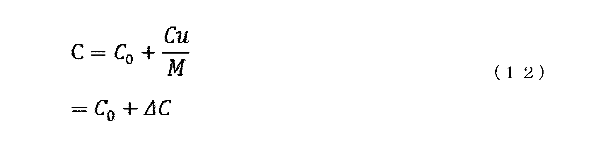
次に、図14の右側に示すように、周波数調整後においては、スイッチ202をオフして、容量バンク100aのM個のうちの半分のキャパシタ102を直列接続から切り離す。この場合、発振器10においては、固定容量104と直列に接続されたM/2個のキャパシタ102とを用いて発振信号を生成することとなる。当該発振器10における総容量値は、以下の数式(13)で示される。

すなわち、本実施形態においては、直列に接続された複数のキャパシタ102を持つ容量バンク100aを利用した場合であっても、直列に接続するキャパシタ102の個数を切り替えることで、発振器10における総容量値を微小な変化幅で変化させることができる。
しかしながら、本実施形態においては、最小容量値Cuと、所望する総容量値の変化幅との差が大きい場合には、容量バンク100aにおける、キャパシタ102の直列数Mが増加し、それに伴いキャパシタ102の直列数を制御するスイッチ202の数も増加する。従って、このような場合、発振器10が設けられる半導体チップの面積の増加につながり、製造コストの増加を招く可能性がある。さらに、キャパシタ102の直列数Mは、整数しか設定することができないため、発振器10の総容量値の可変における自由度が低くなる。従って、このような観点から、上述した第2の実施形態のような、複数のキャパシタ102が並列に接続されている容量バンク100を用いることが好ましい。
<<5.第4の実施形態>>
上述の本開示の実施形態においては、容量バンク100を構成するキャパシタ102の微小容量値ΔCと、各容量バンク100の総容量値とを適切に選択することにより、入力されるデジタル信号に対して、線形的に、連続的に、且つ、微小な変化幅で発振周波数を変化させることができる。さらに、このような容量バンク100は、半導体基板上に設けられることとなる。そこで、本開示の第4の実施形態として、半導体基板上に設けられる容量バンク100について、図15及び図16を参照して説明する。図15は、本開示の第4の実施形態に係るキャパシタ102の構成例を概略的に示すレイアウト図であり、図16は、本実施形態に係る発振器10の構成例を概略的に示すレイアウト図である。なお、これらレイアウト図においては、わかりやすくするために、配線や素子等の図示を省略し、本実施形態に係る要部のみを図示している。
上述の本開示の実施形態においては、容量バンク100を構成するキャパシタ102の微小容量値ΔCと、各容量バンク100の総容量値とを適切に選択することにより、入力されるデジタル信号に対して、線形的に、連続的に、且つ、微小な変化幅で発振周波数を変化させることができる。さらに、このような容量バンク100は、半導体基板上に設けられることとなる。そこで、本開示の第4の実施形態として、半導体基板上に設けられる容量バンク100について、図15及び図16を参照して説明する。図15は、本開示の第4の実施形態に係るキャパシタ102の構成例を概略的に示すレイアウト図であり、図16は、本実施形態に係る発振器10の構成例を概略的に示すレイアウト図である。なお、これらレイアウト図においては、わかりやすくするために、配線や素子等の図示を省略し、本実施形態に係る要部のみを図示している。
詳細には、図15に示すように、本実施形態に係る、1つの容量バンク100は、半導体基板800上に並べられた、複数のキャパシタ102と、MOSトランジスタからなる複数のスイッチ202とを有する。複数のキャパシタ102は、静電容量値が、図15の上下方向に沿って順次段階的に線形的に変化しており、従って、各キャパシタ102が占めるレイアウト面積も順次段階的に線形的に変化している。また、図15に示される例においては、図中の上下方向に沿って7段のキャパシタ対106が設けられており、各キャパシタ対106は、同一静電容量値を持つ、2つのキャパシタ102がスイッチ202を挟んで線対称に配置されている。さらに、各キャパシタ対106においては、2つのキャパシタ102が接続線(配線)204によってスイッチ202と接続されている。
さらに、本実施形態においては、図15のような構成を持つ複数の容量バンク100が半導体基板800上に複数個形成される。例えば、図16に示すように、本実施形態に係る発振器10は、半導体基板800上に、複数の容量バンク100が形成された容量バンク形成領域804を有する。さらに、本実施形態に係る発振器10は、半導体基板800上に、インダクタ300が形成されたインダクタ形成領域802や、負性抵抗回路40等が形成される負性抵抗回路形成領域806や、後述する分周器710が形成される分周器形成領域808等を有していてもよい。
さらに詳細には、複数の容量バンク100は、互いに異なる総容量値を持っていてもよい。具体的には、複数の容量バンク100は、順次段階的に非線形的に増加する総容量値を持っており、従って、各容量バンク100が占めるレイアウト面積も順次段階的に非線形的に変化している。また、容量バンク形成領域804には、固定容量104が設けられていてもよく、さらに精度よく各キャパシタ102を形成するために、発振信号の生成には関与しないダミーキャパシタ(図示省略)が設けられていてもよい。
さらに、インダクタ形成領域802に形成されるインダクタ300は、インダクタ素子であってもよく、配線によって形成されていてもよく、特に限定されるものではない。
なお、図15及び図16に示すレイアウト図は、あくまでも一例であり、本実施形態に係る容量バンク100及び発振器10は、図15及び図16に示されるような形態を有していなくてもよい。
<<6.第5の実施形態>>
<6.1 ラジオ受信機60の構成>
これまで説明した本開示の実施形態に係る発振器10は、例えばラジオ受信機60に適用することができる。そこで、本開示の第5の実施形態として、本実施形態に係る発振器10を適用したラジオ受信機60の一例を、図17を参照して説明する。図17は、本開示の第5の実施形態に係るラジオ受信機60の構成を概略的に示す回路図である。
<6.1 ラジオ受信機60の構成>
これまで説明した本開示の実施形態に係る発振器10は、例えばラジオ受信機60に適用することができる。そこで、本開示の第5の実施形態として、本実施形態に係る発振器10を適用したラジオ受信機60の一例を、図17を参照して説明する。図17は、本開示の第5の実施形態に係るラジオ受信機60の構成を概略的に示す回路図である。
本実施形態に係るラジオ受信機60においては、可変抵抗80の抵抗値をユーザの手動で機械的に変化させることで得られた直流入力電圧により、発振器10における発振周波数の制御を行うことにより、ラジオ放送の選局を行うことができる。
図17に示されるラジオ受信機60においては、アナログ信号である上記入力電圧をデジタル信号に変換し、変換によって得られたデジタル信号により発振器10における総容量値を切り替えることにより、発振器10から所望の周波数を持つ発振信号を得ることができる。従って、本実施形態に係るラジオ受信機60は、このようにして得た発振信号を、ローカル信号として、上記発振器10を含む局部発振信号生成部70からミキサ回路(周波数変換回路)704に供給し、ラジオ信号をIF信号に変換することができる。
詳細には、図17に示すように、ラジオ受信機60の入力されたラジオ信号は、RF増幅器702で増幅され、位相が直交した関係にある局部発振信号が入力される2系統のミキサ回路704で2系統(I信号及びQ信号)のIF信号に変換される。さらに、変換されたIF信号は、バンドパスフィルタ718によってイメージ妨害波が除去され、その後、復調器(復調回路)722によってAM/FM復調され、音声信号となる。
なお、本実施形態に係るラジオ受信機60は、上述したように一度IF信号に変換するスーパーヘテロダイン方式であってもよく、直接ベースバンド信号に変換するダイレクトコンバージョン方式であってもよい。なお、上述したラジオ受信機60のミキサ回路704や復調器722等の各ブロックは、発振器10又は発振器10を含む局部発振信号生成部70と共に、1つの半導体チップ上に設けられることが好ましい。
<6.2 局部発振信号生成部70の構成>
ところで、1つのラジオ受信機60によって、FM/AMラジオ放送を受信する場合には、放送帯域によって受信に使用する局部発振信号(ローカル信号)の周波数が異なる。具体的には、局部発振信号の周波数は、例えば、FM放送の受信時は、IF信号の周波数を150kHzとした場合には、76MHz~108MHzとなる。また、局部発振信号の周波数は、例えば、AM放送の受信時は、IF信号の周波数を55kHzとした場合、575.6kHz~1766.1kHzとなる。
ところで、1つのラジオ受信機60によって、FM/AMラジオ放送を受信する場合には、放送帯域によって受信に使用する局部発振信号(ローカル信号)の周波数が異なる。具体的には、局部発振信号の周波数は、例えば、FM放送の受信時は、IF信号の周波数を150kHzとした場合には、76MHz~108MHzとなる。また、局部発振信号の周波数は、例えば、AM放送の受信時は、IF信号の周波数を55kHzとした場合、575.6kHz~1766.1kHzとなる。
そこで、本実施形態に係るラジオ受信機60においては、AM/FMラジオ放送の両者に対応するために、発振器10によって生成された発振信号を分周する際に、FM受信時とAM受信時で分周器710の分周数を切り替えることができる、局部発振信号生成部70が設けられる。
そこで、上述のように分周数を切り替えることができる、本実施形態に係る局部発振信号生成部70を、図18から図21を参照して説明する。図18は、本実施形態に係る局部発振信号生成部70の構成を概略的に示す回路図である。図19は、本実施形態に係る局部発振信号生成部70における分周を説明するための説明図である。さらに、図20及び図21は、本実施形態に係る局部発振信号生成部70の周波数の変化の一例を示すグラフである。
ところで、FM受信時の局部発振信号の周波数は、76MHz~108MHzの範囲で広がっており、1.42倍以上の周波数変化比となっている。また、AM受信時の局部発振信号の周波数は、575.6kHz~1766.1kHzの範囲で広がっており、3.068倍程度の周波数変化比となっている。従って、FM受信時とAM受信時とでは、局部発振周波数に求められる周波数変化比が大きく異なっている。
しかしながら、AM受信時の局部発振周波数の575.6kHz~1766.1kHzを同一幅で3等分した場合、各範囲における周波数変化比は1.453倍程度となり、FM受信時の周波数変化比と同程度となる。そこで、本実施形態においては、FM受信時の局部発振周波数の範囲を76MHz~110MHz程度に確保し、さらに分周数を選択することによりAM信号の帯域を3等分することにより、1つの発振器10を使用した場合であっても、AM/FM放送の両者に対応することができる。
詳細には、図18に示すように、ミキサ回路704に入力するための局部発振信号を生成する局部発振信号生成部70は、上述した発振器10の他に、発振器10からの発振信号を4分周する分周器710aを有する。さらに、当該局部発振信号生成部70は、分周器710aからの信号をN分周する分周器710bと、分周器710a又は分周器710bからの信号を4分周する分周器710cとを有する。加えて、当該局部発振信号生成部70は、分周器710aからの信号の経路を切り替えるスイッチ208と、分周器710bとスイッチ208とを制御する制御部(制御回路部)210とを有する。さらに、分周器710bは、131分周、90分周、及び62分周の3種類の分周数に切り替えることができるものとする。なお、上述した局部発振信号生成部70は、ラジオ受信機60のミキサ回路704や復調器722等の各ブロックと共に、1つの半導体チップ上に設けられることが好ましい。
次に、図18に示される局部発振信号生成部70の動作を、図19を参照して説明する。まず、FM受信時には、図19の最上段に示されるように、発振器10で生成された発振信号は、1206.4~1752MHzの周波数を持ち、スイッチ208によって分周器710a及び分周器710cを通過する経路を持つこととなる。従って、上記発振信号は、分周器710a及び分周器710cによってそれぞれ4分周され、すなわち、16分周される。その結果、当該局部発振信号生成部70は、76MHz~108MHzの範囲の周波数を持つ局部発振信号を得ることができる。
さらに、AM受信時には、スイッチ208を切り替えて、分周器710aからの発振信号が分周器710bに進むようにする。AM受信時は、AM帯域を3つのバンドMW1(575.KHz~835KHz)、MW2(837.8kHz~1216.7KHz)及びMW3(1216.1KHz~1766.1KHz)に分け、バンドに応じて分周器710bの分周数を切り替えることとなる。
まずは、MW1(575.KHz~835KHz)の周波数を持つAM信号の受信時には、図19の2段目に示されるように、発振器10で生成された発振信号(1206.4~1752MHz)は、分周器710aによって4分周され、さらに、分周器710bによって131分周される。さらに、分周器710bによって分周された信号は、分周器710cによって4分周される。すなわち、上記発振信号は、2096分周されることとなり、当該局部発振信号生成部70は、575.KHz~835KHzの範囲の周波数を持つ局部発振信号を得ることができる。
次に、MW2(837.8kHz~1216.7KHz)の周波数を持つAM信号の受信時には、図19の3段目に示されるように、発振器10で生成された発振信号(1206.4~1752MHz)は、分周器710aによって4分周され、さらに、分周器710bによって90分周される。さらに、分周器710bによって分周された信号は、分周器710cによって4分周される。すなわち、上記発振信号は、1440分周されることとなり、当該局部発振信号生成部70は、837.8kHz~1216.7KHzの範囲の周波数を持つ局部発振信号を得ることができる。
さらに、MW3(1216.1KHz~1766.1KHz)の周波数を持つAM信号の受信時には、図19の4段目に示されるように、発振器10で生成された発振信号(1206.4~1752MHz)は、分周器710aによって4分周され、さらに、分周器710bによって62分周される。さらに、分周器710bによって分周された信号は、分周器710cによって4分周される。すなわち、上記発振信号は、992分周されることとなり、当該局部発振信号生成部70は、1216.1KHz~1766.1KHzの範囲の周波数を持つ局部発振信号を得ることができる。
このように、本実施形態においては、発振器10によって生成された発振信号を分周する際に、FM受信時とAM受信時で分周数を切り替え、さらに、AM信号の帯域を3等分して得られたバンドごとに分周数を切り替える。その結果、本実施形態においては、1つの発振器10を有する局部発振信号生成部70が設けられたラジオ受信機60であっても、AM/FM放送の両者に対応することができる。
このような局部発振信号生成部70によれば、図20に示すように、FM信号受信時においては、入力されるデジタル信号に対して、線形的に、連続的に、且つ、微小な変化幅で変化する周波数を持つ局部発振信号を得ることができることがわかる。また、当該局部発振信号生成部70によれば、図21に示すように、AM信号受信時においても、バンドごとに、入力されるデジタル信号に対して、線形的に、連続的に、且つ、微小な変化幅で変化する周波数を持つ局部発振信号を得ることができることがわかる。
なお、本実施形態においては、各分周器710の分周数や発振器10からの発振信号の周波数については、上述したものに限定されるものではなく、適宜選択することが可能である。さらに、本実施形態においては、局部発振信号生成部70の構成についても、図18に示す構成に限定されるものではなく、適宜変更することが可能である。
<<7.まとめ>>
以上のように、本開示の実施形態によれば、ユーザの手動に応じて、線形的に、連続的に、且つ、微小な変化幅で発振周波数が変化する発振信号を生成することができる発振器10を得ることができる。従って、本実施形態に係る発振器10においては、比較例に係るバリアブルコンデンサ602を使用したラジオ受信機60bと同様の操作性を確保することができる。加えて、本実施形態によれば、バリアブルコンデンサ602やPLLシンセサイザ716を使用しないことから、製造コストや消費電力を抑えることができる。
以上のように、本開示の実施形態によれば、ユーザの手動に応じて、線形的に、連続的に、且つ、微小な変化幅で発振周波数が変化する発振信号を生成することができる発振器10を得ることができる。従って、本実施形態に係る発振器10においては、比較例に係るバリアブルコンデンサ602を使用したラジオ受信機60bと同様の操作性を確保することができる。加えて、本実施形態によれば、バリアブルコンデンサ602やPLLシンセサイザ716を使用しないことから、製造コストや消費電力を抑えることができる。
また、上述した本開示の実施形態に係る発振器10は、ラジオ受信機60に適用するものして説明した。しかしながら、本開示の実施形態に係る発振器10は、ラジオ受信機60に適用されることに限定されるものではなく、スマートウォッチやウェアラブル端末等に搭載される、消費電力を抑えることや小型化が求められる様々な無線通信装置に適用することができる。
<<8.補足>>
以上、添付図面を参照しながら本開示の好適な実施形態について詳細に説明したが、本開示の技術的範囲はかかる例に限定されない。本開示の技術分野における通常の知識を有する者であれば、特許請求の範囲に記載された技術的思想の範疇内において、各種の変更例または修正例に想到し得ることは明らかであり、これらについても、当然に本開示の技術的範囲に属するものと了解される。
以上、添付図面を参照しながら本開示の好適な実施形態について詳細に説明したが、本開示の技術的範囲はかかる例に限定されない。本開示の技術分野における通常の知識を有する者であれば、特許請求の範囲に記載された技術的思想の範疇内において、各種の変更例または修正例に想到し得ることは明らかであり、これらについても、当然に本開示の技術的範囲に属するものと了解される。
また、本明細書に記載された効果は、あくまで説明的または例示的なものであって限定的ではない。つまり、本開示に係る技術は、上記の効果とともに、または上記の効果に代えて、本明細書の記載から当業者には明らかな他の効果を奏しうる。
なお、以下のような構成も本開示の技術的範囲に属する。
(1)
半導体基板上に設けられた複数のキャパシタを含む発振回路と、
アナログ信号をデジタル信号に変換する変換回路と、
前記デジタル信号に基づいて前記キャパシタを切り替えるスイッチ回路と、
を備え、
前記アナログ信号の変化に対して線形的に発振周波数が変化する、
半導体装置。
(2)
前記スイッチ回路は、前記デジタル信号に基づいて、前記発振周波数が線形的に変化するように選択された各容量値を持つ前記複数のキャパシタを切り替える、
上記(1)に記載の半導体装置。
(3)
前記アナログ信号を生成する可変抵抗をさらに備える、上記(1)又は(2)に記載の半導体装置。
(4)
前記複数のキャパシタは、順次、容量値が非線形に増加するように設けられる、上記(2)に記載の半導体装置。
(5)
前記複数のキャパシタは並列に接続される、上記(4)に記載の半導体装置。
(6)
前記各キャパシタは、複数の小キャパシタからなる、上記(1)に記載の半導体装置。
(7)
前記複数の小キャパシタは、前記スイッチ回路によって切り替えられる、上記(6)に記載の半導体装置。
(8)
前記複数の小キャパシタは直列に接続されている、上記(7)に記載の半導体装置。
(9)
前記各小キャパシタは、半導体製造プロセスによって定められる最小単位容量の容量値を持つ、上記(8)に記載の半導体装置。
(10)
前記複数の小キャパシタは並列に接続されている、上記(7)に記載の半導体装置。
(11)
前記複数の小キャパシタは、最小単位容量の容量値を持つ第1の小キャパシタと、前記最小単位容量に微小容量を足し合わせた容量値を持つ第2の小キャパシタとを含み、
前記微小容量は、前記最小単位容量よりも小さい、
上記(10)に記載の半導体装置。
(12)
前記各キャパシタにおける前記複数の小キャパシタは、前記最小単位容量に前記微小容量の2倍の容量値を足し合わせた容量値を持つ第3の小キャパシタをさらに含む、
上記(11)に記載の半導体装置。
(13)
前記最小単位容量又前記微小容量は前記キャパシタごとに異なる、上記(11)又は(12)に記載の半導体装置。
(14)
前記発振回路はインダクタを含む、上記(1)~(13)のいずれか1つに記載の半導体装置。
(15)
前記発振回路からの発振信号をローカル信号として使用する周波数変換回路と、
前記周波数変換回路からの信号に復調する復調回路と、
をさらに備える、上記(1)~(14)のいずれか1つに記載の半導体装置。
(16)
前記発振回路からの発振信号を分周する分周器と、
前記分周器の分周数を切り替える制御回路部と、
をさらに備える、上記(15)に記載の半導体装置。
(17)
前記制御回路部は、入力される信号の周波数に応じて前記分周数を切り替える、上記(16)に記載の半導体装置。
(18)
半導体基板上に設けられた複数のキャパシタを含む発振回路と、
アナログ信号をデジタル信号に変換する変換回路と、
前記デジタル信号に基づいて前記キャパシタを切り替えるスイッチ回路と、
を有し、
前記アナログ信号の変化に対して線形的に発振周波数が変化する、
半導体装置を搭載する無線通信装置。
(1)
半導体基板上に設けられた複数のキャパシタを含む発振回路と、
アナログ信号をデジタル信号に変換する変換回路と、
前記デジタル信号に基づいて前記キャパシタを切り替えるスイッチ回路と、
を備え、
前記アナログ信号の変化に対して線形的に発振周波数が変化する、
半導体装置。
(2)
前記スイッチ回路は、前記デジタル信号に基づいて、前記発振周波数が線形的に変化するように選択された各容量値を持つ前記複数のキャパシタを切り替える、
上記(1)に記載の半導体装置。
(3)
前記アナログ信号を生成する可変抵抗をさらに備える、上記(1)又は(2)に記載の半導体装置。
(4)
前記複数のキャパシタは、順次、容量値が非線形に増加するように設けられる、上記(2)に記載の半導体装置。
(5)
前記複数のキャパシタは並列に接続される、上記(4)に記載の半導体装置。
(6)
前記各キャパシタは、複数の小キャパシタからなる、上記(1)に記載の半導体装置。
(7)
前記複数の小キャパシタは、前記スイッチ回路によって切り替えられる、上記(6)に記載の半導体装置。
(8)
前記複数の小キャパシタは直列に接続されている、上記(7)に記載の半導体装置。
(9)
前記各小キャパシタは、半導体製造プロセスによって定められる最小単位容量の容量値を持つ、上記(8)に記載の半導体装置。
(10)
前記複数の小キャパシタは並列に接続されている、上記(7)に記載の半導体装置。
(11)
前記複数の小キャパシタは、最小単位容量の容量値を持つ第1の小キャパシタと、前記最小単位容量に微小容量を足し合わせた容量値を持つ第2の小キャパシタとを含み、
前記微小容量は、前記最小単位容量よりも小さい、
上記(10)に記載の半導体装置。
(12)
前記各キャパシタにおける前記複数の小キャパシタは、前記最小単位容量に前記微小容量の2倍の容量値を足し合わせた容量値を持つ第3の小キャパシタをさらに含む、
上記(11)に記載の半導体装置。
(13)
前記最小単位容量又前記微小容量は前記キャパシタごとに異なる、上記(11)又は(12)に記載の半導体装置。
(14)
前記発振回路はインダクタを含む、上記(1)~(13)のいずれか1つに記載の半導体装置。
(15)
前記発振回路からの発振信号をローカル信号として使用する周波数変換回路と、
前記周波数変換回路からの信号に復調する復調回路と、
をさらに備える、上記(1)~(14)のいずれか1つに記載の半導体装置。
(16)
前記発振回路からの発振信号を分周する分周器と、
前記分周器の分周数を切り替える制御回路部と、
をさらに備える、上記(15)に記載の半導体装置。
(17)
前記制御回路部は、入力される信号の周波数に応じて前記分周数を切り替える、上記(16)に記載の半導体装置。
(18)
半導体基板上に設けられた複数のキャパシタを含む発振回路と、
アナログ信号をデジタル信号に変換する変換回路と、
前記デジタル信号に基づいて前記キャパシタを切り替えるスイッチ回路と、
を有し、
前記アナログ信号の変化に対して線形的に発振周波数が変化する、
半導体装置を搭載する無線通信装置。
10、10a、90a、90b 発振器
20 LC発振器
30 ADコンバータ
40、40a 負性抵抗回路
50 定電流源
60、60a、60b ラジオ受信機
70 局部発振信号生成部
80 可変抵抗
100、100a、900 容量バンク
102 キャパシタ
104 固定容量
106 キャパシタ対
202、208 スイッチ
204 接続線
206 ノード
210 制御部
300 インダクタ
400 n型MOSトランジスタ
402 p型MOSトランジスタ
502 可変容量
602 バリアブルコンデンサ
702 RF増幅器
704 ミキサ回路
706 水晶発振器
708 位相比較器
710、710a、710b、710c 分周器
712 チャージポンプ
714 ループフィルタ
716 PLLシンセサイザ
718 フィルタ
720 IF増幅器
722 復調器
800 半導体基板
802 インダクタ形成領域
804 容量バンク形成領域
806 負性抵抗回路形成領域
808 分周器形成領域
20 LC発振器
30 ADコンバータ
40、40a 負性抵抗回路
50 定電流源
60、60a、60b ラジオ受信機
70 局部発振信号生成部
80 可変抵抗
100、100a、900 容量バンク
102 キャパシタ
104 固定容量
106 キャパシタ対
202、208 スイッチ
204 接続線
206 ノード
210 制御部
300 インダクタ
400 n型MOSトランジスタ
402 p型MOSトランジスタ
502 可変容量
602 バリアブルコンデンサ
702 RF増幅器
704 ミキサ回路
706 水晶発振器
708 位相比較器
710、710a、710b、710c 分周器
712 チャージポンプ
714 ループフィルタ
716 PLLシンセサイザ
718 フィルタ
720 IF増幅器
722 復調器
800 半導体基板
802 インダクタ形成領域
804 容量バンク形成領域
806 負性抵抗回路形成領域
808 分周器形成領域
Claims (18)
- 半導体基板上に設けられた複数のキャパシタを含む発振回路と、
アナログ信号をデジタル信号に変換する変換回路と、
前記デジタル信号に基づいて前記キャパシタを切り替えるスイッチ回路と、
を備え、
前記アナログ信号の変化に対して線形的に発振周波数が変化する、
半導体装置。 - 前記スイッチ回路は、前記デジタル信号に基づいて、前記発振周波数が線形的に変化するように選択された各容量値を持つ前記複数のキャパシタを切り替える、
請求項1に記載の半導体装置。 - 前記アナログ信号を生成する可変抵抗をさらに備える、請求項1に記載の半導体装置。
- 前記複数のキャパシタは、順次、容量値が非線形に増加するように設けられる、請求項2に記載の半導体装置。
- 前記複数のキャパシタは並列に接続される、請求項4に記載の半導体装置。
- 前記各キャパシタは、複数の小キャパシタからなる、請求項1に記載の半導体装置。
- 前記複数の小キャパシタは、前記スイッチ回路によって切り替えられる、請求項6に記載の半導体装置。
- 前記複数の小キャパシタは直列に接続されている、請求項7に記載の半導体装置。
- 前記各小キャパシタは、半導体製造プロセスによって定められる最小単位容量の容量値を持つ、請求項8に記載の半導体装置。
- 前記複数の小キャパシタは並列に接続されている、請求項7に記載の半導体装置。
- 前記複数の小キャパシタは、最小単位容量の容量値を持つ第1の小キャパシタと、前記最小単位容量に微小容量を足し合わせた容量値を持つ第2の小キャパシタとを含み、
前記微小容量は、前記最小単位容量よりも小さい、
請求項10に記載の半導体装置。 - 前記複数の小キャパシタは、前記最小単位容量に前記微小容量の2倍の容量値を足し合わせた容量値を持つ第3の小キャパシタをさらに含む、
請求項11に記載の半導体装置。 - 前記最小単位容量又は前記微小容量は、前記キャパシタごとに異なる、請求項11に記載の半導体装置。
- 前記発振回路はインダクタを含む、請求項1に記載の半導体装置。
- 前記発振回路からの発振信号をローカル信号として使用する周波数変換回路と、
前記周波数変換回路からの信号に復調する復調回路と、
をさらに備える、請求項1に記載の半導体装置。 - 前記発振回路からの発振信号を分周する分周器と、
前記分周器の分周数を切り替える制御回路部と、
をさらに備える、請求項15に記載の半導体装置。 - 前記制御回路部は、入力される信号の周波数に応じて前記分周数を切り替える、請求項16に記載の半導体装置。
- 半導体基板上に設けられた複数のキャパシタを含む発振回路と、
アナログ信号をデジタル信号に変換する変換回路と、
前記デジタル信号に基づいて前記キャパシタを切り替えるスイッチ回路と、
を有し、
前記アナログ信号の変化に対して線形的に発振周波数が変化する、
半導体装置を搭載する無線通信装置。
Priority Applications (1)
| Application Number | Priority Date | Filing Date | Title |
|---|---|---|---|
| US16/768,779 US11038462B2 (en) | 2017-12-11 | 2018-09-05 | Semiconductor device and wireless communication apparatus |
Applications Claiming Priority (2)
| Application Number | Priority Date | Filing Date | Title |
|---|---|---|---|
| JP2017-236992 | 2017-12-11 | ||
| JP2017236992 | 2017-12-11 |
Publications (1)
| Publication Number | Publication Date |
|---|---|
| WO2019116647A1 true WO2019116647A1 (ja) | 2019-06-20 |
Family
ID=66820804
Family Applications (1)
| Application Number | Title | Priority Date | Filing Date |
|---|---|---|---|
| PCT/JP2018/032801 Ceased WO2019116647A1 (ja) | 2017-12-11 | 2018-09-05 | 半導体装置及び無線通信装置 |
Country Status (2)
| Country | Link |
|---|---|
| US (1) | US11038462B2 (ja) |
| WO (1) | WO2019116647A1 (ja) |
Cited By (1)
| Publication number | Priority date | Publication date | Assignee | Title |
|---|---|---|---|---|
| WO2025211010A1 (ja) * | 2024-04-03 | 2025-10-09 | ソニーセミコンダクタソリューションズ株式会社 | 容量バンク、発振器および位相同期回路 |
Citations (4)
| Publication number | Priority date | Publication date | Assignee | Title |
|---|---|---|---|---|
| JP2000031741A (ja) * | 1998-05-01 | 2000-01-28 | Seiko Epson Corp | 発振周波数制御方泡電圧制御圧電発振器、電圧制御圧電発振器調整システムおよび電圧制御圧電発振器調整方法 |
| JP2002100962A (ja) * | 2000-09-21 | 2002-04-05 | Texas Instr Japan Ltd | 周波数特性調整回路 |
| JP2011520393A (ja) * | 2008-05-07 | 2011-07-14 | クゥアルコム・インコーポレイテッド | Vcoのキャパシタバンクのトリミングとキャリブレーション |
| JP2011155489A (ja) * | 2010-01-27 | 2011-08-11 | Toshiba Corp | 半導体集積回路装置および発振周波数較正方法 |
Family Cites Families (4)
| Publication number | Priority date | Publication date | Assignee | Title |
|---|---|---|---|---|
| US6426680B1 (en) * | 1999-05-26 | 2002-07-30 | Broadcom Corporation | System and method for narrow band PLL tuning |
| US6658748B1 (en) * | 2000-03-02 | 2003-12-09 | Texas Instruments Incorporated | Digitally-controlled L-C oscillator |
| US7483508B2 (en) * | 2001-11-27 | 2009-01-27 | Texas Instruments Incorporated | All-digital frequency synthesis with non-linear differential term for handling frequency perturbations |
| JP5668082B2 (ja) | 2011-01-26 | 2015-02-12 | ルネサスエレクトロニクス株式会社 | 半導体装置 |
-
2018
- 2018-09-05 US US16/768,779 patent/US11038462B2/en active Active
- 2018-09-05 WO PCT/JP2018/032801 patent/WO2019116647A1/ja not_active Ceased
Patent Citations (4)
| Publication number | Priority date | Publication date | Assignee | Title |
|---|---|---|---|---|
| JP2000031741A (ja) * | 1998-05-01 | 2000-01-28 | Seiko Epson Corp | 発振周波数制御方泡電圧制御圧電発振器、電圧制御圧電発振器調整システムおよび電圧制御圧電発振器調整方法 |
| JP2002100962A (ja) * | 2000-09-21 | 2002-04-05 | Texas Instr Japan Ltd | 周波数特性調整回路 |
| JP2011520393A (ja) * | 2008-05-07 | 2011-07-14 | クゥアルコム・インコーポレイテッド | Vcoのキャパシタバンクのトリミングとキャリブレーション |
| JP2011155489A (ja) * | 2010-01-27 | 2011-08-11 | Toshiba Corp | 半導体集積回路装置および発振周波数較正方法 |
Cited By (1)
| Publication number | Priority date | Publication date | Assignee | Title |
|---|---|---|---|---|
| WO2025211010A1 (ja) * | 2024-04-03 | 2025-10-09 | ソニーセミコンダクタソリューションズ株式会社 | 容量バンク、発振器および位相同期回路 |
Also Published As
| Publication number | Publication date |
|---|---|
| US20200321914A1 (en) | 2020-10-08 |
| US11038462B2 (en) | 2021-06-15 |
Similar Documents
| Publication | Publication Date | Title |
|---|---|---|
| TWI528706B (zh) | 基於相位調諧技術調諧lc振盪器頻率的方法和電路 | |
| US7127217B2 (en) | On-chip calibration signal generation for tunable filters for RF communications and associated methods | |
| CN1973437B (zh) | 包括集成频带选择滤波器的电视接收器 | |
| US9312807B2 (en) | Low phase noise voltage controlled oscillators | |
| JP2010056856A (ja) | 半導体集積回路 | |
| WO2007108534A1 (ja) | 電圧制御発振回路 | |
| JPWO2009119042A1 (ja) | 電圧制御発振器、並びにそれを用いたpll回路及び無線通信機器 | |
| JP3956795B2 (ja) | 変調機能付き電圧制御発振器 | |
| CN101263651A (zh) | 振荡器、pll电路和接收机、发送机 | |
| KR100293770B1 (ko) | 직접 변환 방법을 이용하는 선택적 호출 무선 수신기 | |
| JP2008078995A (ja) | 移相回路 | |
| WO2019116647A1 (ja) | 半導体装置及び無線通信装置 | |
| US8718591B2 (en) | Discrete time polyphase mixer | |
| US20050176396A1 (en) | Receiver apparatus | |
| US7098747B2 (en) | Precision tunable voltage controlled oscillation and applications thereof | |
| CN102377429A (zh) | 时钟产生电路和电子装置 | |
| JP2007325083A (ja) | アンテナ入力同調回路 | |
| CN1777035B (zh) | 振荡器、集成电路、通信装置 | |
| JP2004072516A (ja) | テレビジョンチューナ | |
| KR100383187B1 (ko) | 이상기 및 이를 이용한 복조기 | |
| JP3712787B2 (ja) | Fm受信機 | |
| US20060038925A1 (en) | Television receiver arrangement | |
| US20090079880A1 (en) | Television Tuner | |
| US10938344B1 (en) | Systems and methods for frequency-modulation | |
| Jeon et al. | A study on 11 MHz~ 1537 MHz DCO using tri-state inverter for DAB application |
Legal Events
| Date | Code | Title | Description |
|---|---|---|---|
| 121 | Ep: the epo has been informed by wipo that ep was designated in this application |
Ref document number: 18888157 Country of ref document: EP Kind code of ref document: A1 |
|
| NENP | Non-entry into the national phase |
Ref country code: DE |
|
| 122 | Ep: pct application non-entry in european phase |
Ref document number: 18888157 Country of ref document: EP Kind code of ref document: A1 |
|
| NENP | Non-entry into the national phase |
Ref country code: JP |