WO2019098055A1 - 入力装置 - Google Patents
入力装置 Download PDFInfo
- Publication number
- WO2019098055A1 WO2019098055A1 PCT/JP2018/040792 JP2018040792W WO2019098055A1 WO 2019098055 A1 WO2019098055 A1 WO 2019098055A1 JP 2018040792 W JP2018040792 W JP 2018040792W WO 2019098055 A1 WO2019098055 A1 WO 2019098055A1
- Authority
- WO
- WIPO (PCT)
- Prior art keywords
- electrode
- unit
- pressing
- detection
- disposed
- Prior art date
Links
Images


Classifications
-
- G—PHYSICS
- G06—COMPUTING; CALCULATING OR COUNTING
- G06F—ELECTRIC DIGITAL DATA PROCESSING
- G06F3/00—Input arrangements for transferring data to be processed into a form capable of being handled by the computer; Output arrangements for transferring data from processing unit to output unit, e.g. interface arrangements
- G06F3/01—Input arrangements or combined input and output arrangements for interaction between user and computer
- G06F3/03—Arrangements for converting the position or the displacement of a member into a coded form
- G06F3/033—Pointing devices displaced or positioned by the user, e.g. mice, trackballs, pens or joysticks; Accessories therefor
- G06F3/0362—Pointing devices displaced or positioned by the user, e.g. mice, trackballs, pens or joysticks; Accessories therefor with detection of 1D translations or rotations of an operating part of the device, e.g. scroll wheels, sliders, knobs, rollers or belts
-
- G—PHYSICS
- G06—COMPUTING; CALCULATING OR COUNTING
- G06F—ELECTRIC DIGITAL DATA PROCESSING
- G06F3/00—Input arrangements for transferring data to be processed into a form capable of being handled by the computer; Output arrangements for transferring data from processing unit to output unit, e.g. interface arrangements
- G06F3/01—Input arrangements or combined input and output arrangements for interaction between user and computer
- G06F3/02—Input arrangements using manually operated switches, e.g. using keyboards or dials
-
- G—PHYSICS
- G06—COMPUTING; CALCULATING OR COUNTING
- G06F—ELECTRIC DIGITAL DATA PROCESSING
- G06F3/00—Input arrangements for transferring data to be processed into a form capable of being handled by the computer; Output arrangements for transferring data from processing unit to output unit, e.g. interface arrangements
- G06F3/01—Input arrangements or combined input and output arrangements for interaction between user and computer
- G06F3/03—Arrangements for converting the position or the displacement of a member into a coded form
- G06F3/033—Pointing devices displaced or positioned by the user, e.g. mice, trackballs, pens or joysticks; Accessories therefor
- G06F3/0354—Pointing devices displaced or positioned by the user, e.g. mice, trackballs, pens or joysticks; Accessories therefor with detection of 2D relative movements between the device, or an operating part thereof, and a plane or surface, e.g. 2D mice, trackballs, pens or pucks
- G06F3/03547—Touch pads, in which fingers can move on a surface
-
- G—PHYSICS
- G06—COMPUTING; CALCULATING OR COUNTING
- G06F—ELECTRIC DIGITAL DATA PROCESSING
- G06F3/00—Input arrangements for transferring data to be processed into a form capable of being handled by the computer; Output arrangements for transferring data from processing unit to output unit, e.g. interface arrangements
- G06F3/01—Input arrangements or combined input and output arrangements for interaction between user and computer
- G06F3/03—Arrangements for converting the position or the displacement of a member into a coded form
- G06F3/041—Digitisers, e.g. for touch screens or touch pads, characterised by the transducing means
- G06F3/044—Digitisers, e.g. for touch screens or touch pads, characterised by the transducing means by capacitive means
-
- H—ELECTRICITY
- H01—ELECTRIC ELEMENTS
- H01H—ELECTRIC SWITCHES; RELAYS; SELECTORS; EMERGENCY PROTECTIVE DEVICES
- H01H25/00—Switches with compound movement of handle or other operating part
- H01H25/04—Operating part movable angularly in more than one plane, e.g. joystick
-
- H—ELECTRICITY
- H01—ELECTRIC ELEMENTS
- H01H—ELECTRIC SWITCHES; RELAYS; SELECTORS; EMERGENCY PROTECTIVE DEVICES
- H01H89/00—Combinations of two or more different basic types of electric switches, relays, selectors and emergency protective devices, not covered by any single one of the other main groups of this subclass
-
- H—ELECTRICITY
- H03—ELECTRONIC CIRCUITRY
- H03K—PULSE TECHNIQUE
- H03K17/00—Electronic switching or gating, i.e. not by contact-making and –breaking
- H03K17/94—Electronic switching or gating, i.e. not by contact-making and –breaking characterised by the way in which the control signals are generated
- H03K17/945—Proximity switches
- H03K17/955—Proximity switches using a capacitive detector
-
- H—ELECTRICITY
- H03—ELECTRONIC CIRCUITRY
- H03K—PULSE TECHNIQUE
- H03K17/00—Electronic switching or gating, i.e. not by contact-making and –breaking
- H03K17/94—Electronic switching or gating, i.e. not by contact-making and –breaking characterised by the way in which the control signals are generated
- H03K17/96—Touch switches
- H03K17/962—Capacitive touch switches
-
- H—ELECTRICITY
- H03—ELECTRONIC CIRCUITRY
- H03K—PULSE TECHNIQUE
- H03K17/00—Electronic switching or gating, i.e. not by contact-making and –breaking
- H03K17/94—Electronic switching or gating, i.e. not by contact-making and –breaking characterised by the way in which the control signals are generated
- H03K17/965—Switches controlled by moving an element forming part of the switch
- H03K17/975—Switches controlled by moving an element forming part of the switch using a capacitive movable element
-
- H—ELECTRICITY
- H03—ELECTRONIC CIRCUITRY
- H03K—PULSE TECHNIQUE
- H03K17/00—Electronic switching or gating, i.e. not by contact-making and –breaking
- H03K17/94—Electronic switching or gating, i.e. not by contact-making and –breaking characterised by the way in which the control signals are generated
- H03K17/96—Touch switches
- H03K2017/9602—Touch switches characterised by the type or shape of the sensing electrodes
-
- H—ELECTRICITY
- H03—ELECTRONIC CIRCUITRY
- H03K—PULSE TECHNIQUE
- H03K2217/00—Indexing scheme related to electronic switching or gating, i.e. not by contact-making or -breaking covered by H03K17/00
- H03K2217/94—Indexing scheme related to electronic switching or gating, i.e. not by contact-making or -breaking covered by H03K17/00 characterised by the way in which the control signal is generated
- H03K2217/96—Touch switches
- H03K2217/9607—Capacitive touch switches
- H03K2217/960785—Capacitive touch switches with illumination
- H03K2217/96079—Capacitive touch switches with illumination using a single or more light guides
-
- H—ELECTRICITY
- H03—ELECTRONIC CIRCUITRY
- H03K—PULSE TECHNIQUE
- H03K2217/00—Indexing scheme related to electronic switching or gating, i.e. not by contact-making or -breaking covered by H03K17/00
- H03K2217/94—Indexing scheme related to electronic switching or gating, i.e. not by contact-making or -breaking covered by H03K17/00 characterised by the way in which the control signal is generated
- H03K2217/965—Switches controlled by moving an element forming part of the switch
- H03K2217/9651—Switches controlled by moving an element forming part of the switch the moving element acting on a force, e.g. pressure sensitive element
Definitions
- the present disclosure relates to an input device used for input to various electronic devices.
- a conventional input device comprises an input unit and a detection unit.
- the input unit includes an input unit, a rotating electrode unit, and a holding electrode unit.
- the input unit includes a rotating unit that rotates.
- the rotating electrode unit is rotated by the rotation of the rotating unit.
- the holding electrode unit is disposed at a position facing the rotating electrode unit.
- the holding electrode unit changes its electrical state with the rotating electrode unit by the rotation of the rotating electrode unit.
- the detection unit has a first detection electrode unit and a substrate unit.
- the substrate portion is provided with electronic components and has an electronic circuit. Further, in the substrate portion, the first detection electrode portion is formed on the surface opposite to the surface on which the electronic circuit is formed.
- the first detection electrode unit is disposed at a position facing the holding electrode unit. The capacitance of the first detection electrode unit changes due to the rotation of the rotation unit.
- Patent Document 1 an input device disclosed in Patent Document 1 is known.
- the input device is disposed in a first region that is disposed so as to overlap the rotating portion having an opening and the opening of the rotating portion in a plan view and overlaps the opening in the plan view. It has a pressing member which transmits light, a rotating electrode unit having a first electrode body which rotates according to the rotation of the rotating unit, and a second electrode body, and at least a part of the second electrode body is the rotation.
- the second electrode body is disposed so as to face the electrode portion, and the second electrode body is disposed so as to face the holding electrode portion, the holding electrode portion coming into contact with and separated from the first electrode body by rotation of the rotary electrode portion.
- the receiving electrode is disposed to overlap the first receiving electrode in the plan view.
- a capacitance between the first receiving electrode and the first transmitting electrode is changed by the rotation of the rotating electrode portion, and the substrate portion and the first transmitting electrode in the first region Light is transmitted through the pressing member.
- the input device of the present disclosure can transmit light incident from a first direction in a second direction opposite to the first direction in the first region.
- FIG. 3 Perspective view of the display device of the present disclosure Development perspective view of the display device of the present disclosure Perspective view of the input unit of the present disclosure Exploded perspective view of the input unit shown in FIG. 3 Exploded perspective view of the input unit shown in FIG. 3 Schematic of detection unit of the present disclosure Partial cross-sectional view of the detection unit shown in FIG. Schematic explaining the cross section of the display device Diagram for explaining the operation of the display device Diagram for explaining the operation of the display device Diagram for explaining the operation of the display device
- an opaque substrate such as a printed circuit board is used for the substrate unit. Therefore, light incident on the input device from the first direction (lower side) than the input device was less likely to transmit in the second direction (upper direction) than the input device.
- first direction will be described as “down” and the second direction will be described as “upper”.
- first direction is described as “down” and the second direction is described as “upper”, the “first direction” and the “second direction” may be directions opposite to each other.
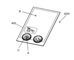
- FIG. 1 is a perspective view of the display device 2000
- FIG. 2 is an exploded perspective view of the display device 2000.
- An example of the display device 2000 includes, for example, a touch panel.
- the display device 2000 includes a cover member 51, an electrode substrate 52, and a display 400. Below the display 400, a controller 500 (see FIG. 2) is formed.
- the display device 2000 includes an input device 1000.
- the input device 1000 includes an input unit 100 fixed to the cover member 51 by a fixing member 300 and a detection unit 200 formed on the electrode substrate 52.
- the input device 1000 is configured to allow the light emitted upward from the display 400 disposed below the detection unit 200 (details will be described later) to pass through the input unit 100 and the detection unit 200.
- FIG. 3 is a perspective view of the input unit 100.
- FIG. 4 is an exploded perspective view of the input unit 100 as viewed from above.
- FIG. 5 is an exploded perspective view of the input unit 100 as viewed from below.
- the input device 1000 includes the input unit 100 and the detection unit 200, and the detection unit 200 is disposed below the input unit 100.
- the detection unit 200 will be described later with reference to FIG.
- the input unit 100 has a rotating portion 11, a pressing member 12 and a guide portion 13.
- the rotating unit 11 is rotated by the application of a force, for example, by a user, a robot, or a mechanism.
- the pressing member 12 is disposed inside the outer edge of the rotating portion 11. Further, as shown in FIG. 4, the pressing member 12 is composed of a main body portion 12 a, a holding portion 12 b, and a pressing portion 12 c, and at least the main body portion 12 a can transmit light.
- the rotary electrode unit 20 is disposed below the rotary unit 11, and the rotary electrode unit 26 (see FIG. 5) is formed on the rotary electrode unit 20 so as to be exposed to the lower surface.
- the rotating electrode body 26 (see FIG. 5) is rotated by the rotation of the rotating portion 11.
- the metal is insert-formed on the lower surface of the rotary electrode portion 20 which is entirely made of resin so as to be exposed from the resin.
- the portion where metal is exposed corresponds to the rotary electrode body 26, and the remaining portion is the resin 25b.
- the rotary electrode unit 20 is disposed on the holding member 31, and the holding electrode unit 30, the reference electrode unit 60, and the pressing electrode unit 80 are disposed below the holding member 31. That is, the holding electrode body 32 (the holding electrode portion 30) is disposed to face the rotary electrode body 26 via the holding member 31. Then, due to the rotation of the rotary electrode unit 20, the electrical state between the holding electrode body 32 and the rotary electrode body 26 changes.
- FIG. 6 is a schematic view of a detection unit 200 of the present disclosure.
- FIG. 7 is a partial cross-sectional view along line YY of the detection unit 200 shown in FIG.
- the detection unit 200 is formed on the electrode substrate 52, and the cover member 51 is stacked on the electrode substrate on which the detection unit 200 is formed.
- the electrode substrate 52 and the cover member 51 are not shown in FIG.
- the detection unit 200 includes a first detection electrode unit 40 located at the periphery and a second detection electrode unit 90 located at the center.
- the first detection electrode unit 40 includes a detection electrode body 41 having a pair of the reception electrode 41a and the transmission electrode 41b, a detection electrode body 42 having a pair of the reception electrode 42a and the transmission electrode 42b, a reception electrode 43a and a transmission electrode 43b And a detection electrode body 43 having a pair.
- Four second detection electrode portions 90 each having the reception electrode 90 a and the transmission electrode 90 b as a pair are formed.
- the receiving electrode 42 a is disposed on the upper surface of the electrode substrate 52
- the transmitting electrode 42 b is disposed on the lower surface of the electrode substrate 52.
- the receiving electrode 42a and the transmitting electrode 42b are opposed in the vertical direction.
- the positional relationship between the receiving electrode 42a and the transmitting electrode 42b has been described here, the positional relationship between the receiving electrode 41a and the transmitting electrode 41b and the positional relationship between the receiving electrode 43a and the transmitting electrode 43b are the same.
- FIG. 8 is a schematic view for explaining a cross section of the display device shown in FIG.
- a detection unit 200 is disposed below the input unit 100.
- the detection unit 200 is only schematically shown, and for example, the transmission electrodes 42 b and 43 b are not illustrated.
- the detection electrode body 42 (see FIG. 6) is located below the pressing electrode portion 80 (see FIG. 4), and the detection electrode bodies 41 and 42 (FIG. 6) under the two holding electrode bodies 32 (see FIG. 4). See) is located.
- the reception electrode unit 44 (see FIG. 6) is located below the reference electrode unit 60 (see FIG. 4).
- the reception electrode 41a and the transmission electrode 41b are capacitively coupled, and the rotation of the rotation unit 11 causes the reception electrode 41a and the transmission electrode 41b (or the reception electrode 42a and the transmission electrode 42b) And the capacitance between them changes.
- the first detection electrode unit 40 (the reception electrode 41 a, the transmission electrode 41 b, the reception electrode 42 a, the transmission electrode 42 b, the reception electrode 43 a, the transmission electrode 43 b, the reception electrode unit 44) is formed in the substrate unit 50. It is done.
- the substrate unit 50 transmits light in a region (first region A) opposed to the main body 12a (transmission portion) of the pressing member 12 (see FIG. 8).
- the input device 1000 includes the pressing member 12 disposed inside the outer edge of the rotating portion 11 and transmitting light, and the substrate portion 50 transmitting light in the first region A facing the pressing member 12.
- the substrate unit 50 is configured of the cover member 51 and the electrode substrate 52. With this configuration, light that has entered the first region A from below the substrate unit 50 can pass through the substrate unit 50 and the pressing member 12 and travel upward from the pressing member 12. Therefore, the input device 1000 can visually recognize an object located below the substrate unit 50 through the pressing member 12 and the substrate unit 50.
- the input device 1000 includes an input unit 100 and a detection unit 200. As described above, the input device 1000 is configured to be able to transmit light incident from below the detection unit 200 to the upper side of the input unit 100. Further, the input device 1000 receives mechanical input by the input unit 100. Here, mechanical input includes, for example, rotation, pushing, pulling, and sliding. Then, the detection unit 200 converts at least one input of the inputs input to the input unit 100 into a change in capacitance.
- FIG. 4 is an exploded perspective view of the input unit 100 shown in FIG. 3 as viewed from above.
- FIG. 5 is an exploded perspective view of the input unit 100 shown in FIG. 3 as viewed from below.
- the input unit 100 includes a rotating portion 11, a rotating electrode portion 20 including a rotating electrode body 26, a holding electrode portion 30 including two holding electrode bodies 32, a reference electrode portion 60, a switch body 70, and a pressing electrode portion And 80.
- the input unit 100 has a rotating portion 11, a pressing member 12 and a guide portion 13.
- the rotating portion 11 is formed in an annular shape having a circular outer edge and a circular inner edge.
- the rotating portion 11 is rotatably held by the holding member 31.
- the pressing member 12 and the guide portion 13 are disposed inside the inner edge of the rotating portion 11.
- the ring shape of the rotating portion 11 may be a polygon. For example, it may be annular with the outer edge of the polygon and the inner edge of the polygon. In addition, in the ring shape of the rotating portion 11, the shape of the inner edge and the shape of the outer edge do not have to match.
- the ring shape of the rotating portion 11 may be an annular shape having a polygonal outer edge and a circular inner edge, or may be an annular shape having a circular outer edge and a polygonal inner edge.
- the inner edge and the outer edge of the rotating portion 11 do not have to be strictly circular or polygonal, respectively, and may be annularly formed by a combination of curves and straight lines.
- the inner edge and the outer edge of the rotating portion 11 may have an oval shape, an approximate circle, or an approximate polygon obtained by rounding the corners of a polygon with a curve.
- the rotating portion 11 may have an opening.
- the pressing member 12 has a main body portion 12a, a holding portion 12b, and a pressing portion 12c.
- the body portion 12a is transparent, for example, containing glass, polycarbonate, polystyrene, acrylic or the like, and can transmit light.
- the main body portion 12 a is disposed inside the inner edge of the rotating portion 11. That is, the opening of the rotating portion 11 and the pressing portion 12c overlap in a plan view.
- the main body portion 12 a is located inside the inner edge of the rotating portion 11 and exposed outward from the input device 1000. In other words, the main body 12 a is exposed to the outside from the input device 1000 inside the inner edge of the guide 13.
- the term "transparent” may be colored or transparent. Further, the main body 12a may be transparent as long as visible light incident from below can be viewed from above. Therefore, the main body 12a may be formed to reflect light from above but transmit light from below. That is, the main body 12a may be, for example, a magic mirror.
- the pressing portion 12c protrudes from the main body portion 12a.
- the pressing portion 12 c is disposed above the switch body 70.
- the guide part 13 is arrange
- the pressing portion 12c may be made of the same material as the main portion 12a.
- the pressing portion 12c may be transparent or opaque.
- the pressing portion 12c may be integral with or separate from the main body 12a.
- the holding portion 12 b protrudes from the main body portion 12 a. And the holding part 12b is arrange
- the holding portion 12 b is held between the upper surface of the holding member 31 and the lower surface of the guide portion 13. Further, the holding portion 12 b is held so that the pressing portion 12 c can move up and down.
- the holding portion 12b may be made of the same material as the main portion 12a or the pressing portion 12c.
- the holding portion 12b may be transparent or opaque. Further, the holding portion 12b may be integral with or separate from the main body portion 12a.
- the guide portion 13 is disposed in the ring of the rotating portion 11. Moreover, the guide part 13 is arrange
- the rotary electrode unit 20 has a rotary unit 25 and a rotary electrode body 26 (first electrode body).
- the rotating portion 25 is formed in an annular and cylindrical shape.
- the rotating portion 25 is formed of an insulating resin. Further, on the upper surface of the rotating portion 25, an uneven portion 25 a having a plurality of concave portions and a plurality of convex portions is formed.
- the rotary unit 25 holds the rotary electrode 26 on the lower surface.
- the rotary electrode body 26 has an outer peripheral portion 26a (see FIG. 5) in which notches are formed at equal intervals, and an inner peripheral portion 26b (see FIG. 5) positioned closer to the inner edge of the rotary electrode portion 20 than the outer peripheral portion 26a. , And an annular conductor. Therefore, at the cut position of the rotary electrode body 26, the rotary portion 25 is exposed, and the exposed portion of the rotary portion 25 is shown as the resin 25b.
- the holding electrode unit 30 has a holding member 31, a holding electrode body 32, and a click spring 33.
- the holding member 31 is formed in an annular and cylindrical shape. Further, the holding member 31 is formed with a plurality of holes penetrating from the lower surface to the upper surface.
- the holding member 31 rotatably holds the rotating unit 25.
- the holding member 31 holds the holding electrode body 32 on the lower surface.
- the holding electrode body 32 is disposed at a position facing the rotating electrode body 26. Further, one holding electrode body 32 has a brush 32a and a main body portion 32c, and the other holding electrode body 32 has a brush 32b and a main body portion 32d.
- the brush 32a and the main body 32c are integrally formed of a conductor. Further, the brush 32b and the main body 32d are integrally formed of a conductor.
- the brush 32a and the brush 32b protrude upward through different holes of the corresponding holding member 31, and contact the outer peripheral portion 26a or the rotating portion 25 (resin 25b) of the rotary electrode body 26.
- the main body 32 c and the main body 32 d are held by the lower surface of the holding member 31.
- the click spring 33 has a contact pressure portion 33a.
- the click spring 33 is an annular metal body, and the contact pressure portion 33a has elasticity.
- the click spring 33 is held by the holding member 31 so as to bring the contact portion 33a into contact with the uneven portion 25a.
- the reference electrode unit 60 has a brush 60a and a main body 60b.
- the brush 60a and the main body 60b are integrally formed of a conductor.
- the reference electrode portion 60 is held on the lower surface of the holding member 31.
- the brush 60 a protrudes upward through the hole of the holding member 31 at a position different from the brush 32 a and the brush 32 b and contacts the inner circumferential portion 26 b of the rotary electrode 26.
- the switch body 70 is located below the guide portion 13.
- the switch body 70 is disposed on the holding member 31 and is disposed below the pressing portion 12 c of the pressing member 12. That is, the switch body 70 is sandwiched by the holding member 31 and the pressing portion 12 c.
- the switch body 70 has a first terminal and a second terminal. The first terminal and the second terminal are electrically connected by applying a pressing force. Then, the first terminal of the switch body 70 is electrically connected to the reference electrode unit 60.
- the switch body 70 preferably uses an electronic component that reduces the resistance value by receiving a pressing force.
- an electronic component a push switch, a pressure sensor, a membrane switch etc. are mentioned, for example.
- a click feeling can be generated by pressing the switch body 70.
- a pressure sensor is used as the switch body 70
- an electrical signal can be output according to the pressing force applied to the switch body 70.
- the membrane switch is used as the switch body 70, the amount of movement of the pressing member 12 in the vertical direction can be suppressed.
- the pressing electrode portion 80 is a conductor held on the lower surface of the holding member 31. Further, the pressing electrode unit 80 is disposed at a position between the reference electrode unit 60 and the holding electrode body 32 in the rotational direction. The pressing electrode unit 80 is electrically connected to the second terminal of the switch body 70. Therefore, the press electrode unit 80 is electrically conducted to the reference electrode unit 60 through the switch body 70 in a state where the first terminal and the second terminal of the switch body are electrically conducted.
- FIG. 6 is a schematic view of the detection unit 200.
- FIG. 7 is a cross-sectional view taken along line YY shown in FIG.
- FIG. 8 is a schematic view illustrating the cross section of the display device of the input device 1000. As shown in FIG. The portion of the input unit 100 corresponds to the cross-sectional view along the line XX shown in FIG.
- the detection unit 200 has a first detection electrode unit 40 and a second detection electrode unit 90.
- the first detection electrode unit 40 and the second detection electrode unit 90 are formed on the electrode substrate 52 (see FIG. 8).
- the capacitance is changed by the operation of the input unit 100.
- the first detection electrode unit 40 includes a detection electrode body 41, a detection electrode body 42, a detection electrode body 43, and a reception electrode portion 44.
- the detection electrode body 41 has a reception electrode 41a and a transmission electrode 41b.
- the receiving electrode 41a and the transmitting electrode 41b are electrodes having conductivity.
- the receiving electrode 41a is electrically insulated from the transmitting electrode 41b. Further, the receiving electrode 41a is formed in an annular shape, and is disposed above the transmitting electrode 41b. Furthermore, between the receiving electrode 41a and the transmitting electrode 41b, for example, an insulating layer such as air, resin, or glass is disposed. In the input device 1000, the insulating layer is borne by an electrode substrate 52 described later. That is, the electrode substrate 52 is disposed between the reception electrode 41a and the transmission electrode 41b. Then, the capacitance between the transmission electrode 41 b and the reception electrode 41 a is changed by the rotation of the rotation unit 11 of the input unit 100.
- the detection electrode body 42 has a reception electrode 42 a and a transmission electrode 42 b.
- the receiving electrode 42 a and the transmitting electrode 42 b are electrodes having conductivity.
- the receiving electrode 42a is electrically insulated from the transmitting electrode 42b.
- the receiving electrode 42a is formed in an annular shape, and is disposed above the transmitting electrode 42b.
- an insulating layer such as air, resin, or glass is disposed between the input device 1000.
- the insulating layer is borne by an electrode substrate 52 described later. That is, the electrode substrate 52 is disposed between the receiving electrode 42a and the transmitting electrode 42b.
- the electrostatic capacitance between the transmission electrode 42 b and the reception electrode 42 a is changed by the rotation of the rotation unit 11 of the input unit 100.
- the detection electrode body 43 has a reception electrode 43a and a transmission electrode 43b.
- the receiving electrode 42 a and the transmitting electrode 42 b are electrodes having conductivity.
- the receiving electrode 43a is electrically insulated from the transmitting electrode 43b. Further, the receiving electrode 43a is annularly formed, and is disposed above the transmitting electrode 43b. Furthermore, between the receiving electrode 43a and the transmitting electrode 43b, for example, an insulating layer such as air, resin, or glass is disposed. In the input device 1000, the insulating layer is borne by an electrode substrate 52 described later. That is, the electrode substrate 52 is disposed between the reception electrode 43a and the transmission electrode 43b.
- the electrostatic capacitance between the transmission electrode 43 b and the reception electrode 43 a changes when the switch body 70 is pressed.
- the switch body 70 is pressed by the pressing portion 12 c when the pressing member 12 is pressed. That is, the electrostatic capacitance between the transmission electrode 43 b and the reception electrode 43 a changes when the pressing member 12 is pressed.
- the reception electrode unit 44 is a reference of detection of the detection electrode body 41, the detection electrode body 42, and the detection electrode body 43.
- the receiving electrode unit 44 is a conductive electrode disposed at a position facing the reference electrode unit 60 (see FIG. 4).
- the receiving electrode unit 44 is electrically connected to the ground and has a ground potential.
- the first detection electrode unit 40 is configured to detect the rotation and the pressing by the electrically independent electrodes (the detection electrode body 41 or the detection electrode body 42 and the detection electrode body 43). Thereby, the erroneous detection of rotation or a press can be suppressed. Further, by having the detection electrode body 41 and the detection electrode body 42, the first detection electrode unit 40 can output an electrical signal according to the rotation direction of the rotation unit 11. Therefore, when outputting that the rotation unit 11 is rotating as an electric signal, the first detection electrode unit 40 may have either the detection electrode body 41 or the detection electrode body 42.
- the reception electrodes 41a, 42a, 43a and the transmission electrodes 41b, 42b, 43b may be metal electrodes containing metals such as copper, silver, aluminum, gold and the like, and conductive metal oxides such as ITO (Indium Tin Oxide).
- a transparent electrode including a conductive material, a conductive organic material, or a carbon material such as graphene may be used.
- the substrate unit 50 has a cover member 51 and an electrode substrate 52.
- the cover member 51 has a first surface and a second surface.
- the first surface of the cover member 51 faces the holding electrode unit 30.
- the second surface is the back surface of the first surface, and is located below the second surface.
- the cover member 51 has a hardness higher than or equal to that of the electrode substrate 52 and has translucency in at least a first region A facing the main body 12 a of the pressing member 12.
- the electrode substrate 52 is, for example, a film having a hardness similar to that of the cover member 51 or a hardness lower than that of the electrode substrate 52, and has translucency in at least the first region A facing the main body 12a of the pressing member 12.
- the substrate unit 50 is configured to allow light to pass from the lower surface to the upper surface at least in the first region A.
- Receiving electrodes 41 a, 42 a and 43 a are formed on the top surface of the electrode substrate 52.
- transmission electrodes 41 b, 42 b and 43 b are formed on the lower surface of the electrode substrate 52.
- the electrode substrate 52 may be formed by overlapping a plurality of films, or may be a single film. In the case of a plurality of films, the receiving electrodes 41a, 42a and 43a may not be formed on the uppermost surface, and the transmitting electrodes 41b, 42b and 43b may not be formed on the lowermost surface.
- the capacitance of the second detection electrode unit 90 changes as the object contacts or approaches the pressing member 12.
- examples of the object include human fingers and robot arms.
- the second detection electrode unit 90 is formed in a first region A of the electrode substrate 52 facing the main body 12 a of the pressing member 12.
- the second detection electrode unit 90 has light transparency.
- the second detection electrode unit 90 is formed on the same plane as the first detection electrode unit 40, but may be formed on a plane different from the first detection electrode unit 40.
- the second detection electrode unit 90 has four electrically independent electrodes and is arranged in a cross shape. Each of the four electrodes of the second detection electrode unit has a reception electrode 90 a and a transmission electrode 90 b, and is disposed on the electrode substrate 52.
- the receiving electrode 90a is annularly formed, and is disposed above the transmitting electrode 90b. That is, the electrode substrate 52 is disposed as an insulating layer between the reception electrode 90a and the transmission electrode 90b.
- the electrostatic capacitance between the receiving electrode 90 a and the transmitting electrode 90 b is changed by the contact or proximity of the object to the pressing member 12.
- the degree of light transmission of the second detection electrode unit 90 is transparent to such an extent that light incident from below the electrode substrate 52 can enter the pressing member 12 in a state where the second detection electrode unit 90 is formed on the electrode substrate 52
- the second detection electrode unit 90 may use a metal electrode containing a metal such as copper, silver, aluminum, or gold as long as the above-described light transmittance can be satisfied, and the conductive property such as ITO (Indium Tin Oxide)
- ITO Indium Tin Oxide
- a transparent electrode including a metal oxide, a conductive organic material, or a carbon material such as graphene may be used.
- a thin wire is formed of metal
- a thin wire is formed of metal in a mesh shape
- a thin wire formed of metal is blackened, or the metal electrode is formed in any direction. Is preferred.
- the rotating unit 25 is rotated by the rotation of the rotating unit 11.
- the rotating electrode body 26 is held on the lower surface of the rotating portion 25 (see FIG. 5). Therefore, the rotating electrode body 26 rotates with the rotating portion 11.
- the rotary electrode body 26 is in contact with the brush 60 a (see FIG. 4) of the reference electrode unit 60 at the inner circumferential portion 26 b.
- the rotary electrode body 26 contacts the brush 32 a and the brush 32 b of the holding electrode body 32 at the outer peripheral portion 26 a of the rotary electrode body 26.
- the receiving electrode 41a faces the main body 32d. Therefore, the capacitance between the reception electrode 41a and the transmission electrode 41b changes due to the change in the electrical state of the main body 32d.
- the receiving electrode 42a faces the main body 32c. Therefore, the capacitance between the receiving electrode 42a and the transmitting electrode 42b changes due to a change in the electrical state of the main body 32c.
- the change in electrical state between the main body 60b and the main body 32c is different from the change in electrical state between the main body 60b and the main body 32d. Therefore, the capacitance change between the reception electrode 42a and the transmission electrode 42b is different from the capacitance change between the reception electrode 41a and the transmission electrode 41b.
- the pressing member 12 presses the switch body 70 with the pressing portion 12 c by being pressed downward.
- the reference electrode portion 60 and the pressing electrode portion 80 are electrically connected. That is, the reference electrode unit 60 and the pressing electrode unit 80 are in a conductive state when the pressing member 12 is pressed, and are in a disconnected state when the pressing member 12 is not pressed.
- the receiving electrode 43 a faces the pressing electrode unit 80. Therefore, the capacitance between the receiving electrode 43a and the transmitting electrode 43b changes due to the change in the electrical state of the pressing electrode unit 80.
- the input device 1000 can rotate the rotating unit 11, press the pressing member 12, approach or contact an object to the pressing member 12, to set the static state between the reception electrode and the transmission electrode corresponding to each operation. Change in capacitance. Thereby, the input device 1000 can output these electrostatic capacitance changes as an electrical signal.
- the input device 1000 light is transmitted through at least a first region A (see FIG. 8) of the substrate unit 50 facing the main body 12a of the pressing member 12. Therefore, when the pressing member 12 is viewed from above the pressing member 12, the portion below the substrate unit 50 can be viewed.
- the input device 1000 also has a second detection electrode unit 90 at a position facing the pressing member 12. Further, the second detection electrode unit 90 is formed to be able to transmit light. Therefore, the input device 1000 can perform touch input and hover input with the pressing member 12 while looking at an object located below the substrate unit 50.
- the input device 1000 is configured to conduct the reference electrode unit 60 and the pressing electrode unit 80 by pressing the pressing member 12 downward, and to change the capacitance of the first detection electrode unit 40. Therefore, the input device 1000 can realize the pressing input in addition to the rotation input while looking at the lower side of the substrate unit 50.
- the input device 1000 forms the detection electrode body 41 or the detection electrode body 42 on the same plane as the detection electrode body 43, there is no need to provide a separate circuit board for detecting a pressure. It is possible to realize miniaturization and thinning.
- the switch body 70 which brings the reference electrode portion 60 and the pressing electrode portion 80 into conduction by pressing is disposed at a position close to the outer edge of the pressing member 12.
- the switch body 70 is disposed at a position closer to the rotating portion 11 than the main body portion 12 a visible from above the input device 1000. Therefore, when the input device 1000 views the pressing member 12 from above the pressing member 12, the switch body 70 can be prevented from blocking the lower side than the substrate unit 50, so that the visibility can be improved.
- FIG. 8 is a schematic diagram for explaining a cross section of the display device 2000.
- FIG. 9 is a diagram for explaining the operation of the display device 2000.
- 10 and 11 are diagrams for explaining the operation of the display device.
- the display device 2000 includes an input device 1000, a display 400, and a controller 500.
- the input device 1000 includes an input unit 100, a detection unit 200, and a fixing member 300.
- the substrate unit 50 of the detection unit 200 is configured of a transparent touch panel having a cover member 51.
- the substrate unit 50 is formed larger than the input unit 100. That is, the input device 1000 can transmit light by the pressing member 12 and the second area B outside the input unit 100.
- the fixing member 300 is disposed between the input unit 100 and the detection unit 200, and holds the input unit 100 and the detection unit 200.
- the detection unit 200 is electrically connected to the controller 500.
- the display 400 is configured of, for example, a liquid crystal display, an organic electroluminescence (organic EL) display, a transparent display, or the like.
- the display 400 is disposed below the input device 1000. Therefore, the content displayed on the display 400 can be viewed from above the display device 2000 in the first area A and the second area B.
- the displays 400 located at positions corresponding to the first area A and the second area B may be the same display or separate displays.
- the display 400 is electrically connected to the controller 500.
- the controller 500 is electrically connected to the detection unit 200 and the display 400.
- the controller 500 detects the capacitance change in the detection unit 200 to determine the input (rotation, press, touch or approach) received by the input unit 100. Then, the controller 500 controls the content displayed on the display 400 according to the input content.
- FIGS. 9 to 11. 10 and 11 are diagrams for explaining the operation of the display device 2000.
- the controller 500 in the first area A causes the operator to The selected "Temp” is displayed in the second area B.
- controller 500 determines that the content selected by the operator has been determined, and changes the content displayed in first area A and second area B. (See Figure 11).
- the controller 500 changes the display 400 to a temperature setting screen.
- the temperature setting screen in the first area A, the relationship between the rotational direction of the rotating portion 11 and the temperature rise and fall is displayed, and in the second area B, the current set temperature is displayed. Then, the operator can change the temperature setting by rotating the rotating unit 11.
- the display region is divided into the first region A and the second region B of the input device 1000. Then, the controller 500 controls the content displayed in the first area A and the second area B. Therefore, the operator can operate the display device 2000 more easily.
- the controller 500 may display the same content as the content selected in the first region A in the second region B, and the content based on the content selected in the first region A is the second region B. It may be displayed on the screen. For example, a folder may be displayed in the first area A, and the contents of the selected folder may be displayed in the second area B. Further, for example, an icon may be displayed in the first area A, and a description on the selected icon may be displayed in the second area B.
- the input device 1000 is disposed so as to overlap the rotating portion 11 having the opening with the opening of the rotating portion 11 in plan view, and transmits light in the first region A overlapping in plan view with the opening.
- a rotating electrode unit 20 having a first electrode body (rotating electrode body 26) and a second electrode body (holding electrode body 32).
- the brush 32 a / the brush 32 b) of the two-electrode assembly (holding electrode assembly 32) is disposed to face the rotating electrode unit 20, and the second electrode assembly (holding A holding electrode unit 30 in which the electrode body 32) is in contact with and separated from the first electrode body (rotating electrode body 26), a first detection electrode unit 40 arranged to face the holding electrode unit 30, and a first detection electrode unit And a substrate unit 50 on which 40 is formed.
- the 1st sensing electrode part 40 is the 1st receiving electrode (receiving electrode 41a / receiving electrode 42a) arranged so that it may overlap with the 2nd electrode body (holding electrode body 32) in plane view, and the 1st in plane view.
- the capacitance between the first transmission electrode (the transmission electrode 41 b / the transmission electrode 42 b) changes with the rotation of the rotary electrode unit 20, and in the first region A, through the substrate unit 50 and the pressing member 12. Light is transmitted.
- a reference electrode unit 60 electrically connected to the holding electrode unit 30 through the rotary electrode unit 20, and a first surface opposite to the first surface where the substrate unit 50 faces the holding electrode unit 30.
- a pressing electrode unit 80 which is electrically connected to the reference electrode unit 60 by pressing the pressing member 12 in a first direction (direction from the top to the bottom) directed to the side second surface.
- the first detection electrode unit 40 is disposed so as to overlap the second reception electrode (reception electrode 43a) disposed so as to overlap the pressing electrode unit 80 in a plan view and the second reception electrode (reception electrode 43a) in a plan view And a second transmission electrode (transmission electrode 43b).
- the capacitance between the second reception electrode (reception electrode 43a) and the second transmission electrode (transmission electrode 43b) changes as the pressing member 12 is pressed downward.
- the input device 1000 of the present disclosure further includes a switch body 70 that electrically connects the reference electrode unit 60 to the pressing electrode unit 80 by pressing the pressing member 12 downward.
- the pressing member 12 has a main body portion 12 a that transmits light, and a pressing portion 12 c that protrudes from the main body portion 12 a.
- the switch body 70 is disposed below the pressing portion 12 c of the pressing member 12.
- the input device 1000 of the present disclosure further includes a second detection electrode unit 90 disposed on the substrate unit 50 so as to overlap with the pressing unit 12 c of the pressing member 12 in a plan view.
- the second detection electrode unit 90 detects whether an object (for example, a finger C) contacts or approaches the pressing unit 12c.
- the input device according to the present disclosure has an effect of transmitting light incident from the first direction more than the input device in the second direction more than the input device, and is useful when used in various electronic devices and the like.
Landscapes
- Engineering & Computer Science (AREA)
- General Engineering & Computer Science (AREA)
- Theoretical Computer Science (AREA)
- Human Computer Interaction (AREA)
- Physics & Mathematics (AREA)
- General Physics & Mathematics (AREA)
- Switches That Are Operated By Magnetic Or Electric Fields (AREA)
- Input From Keyboards Or The Like (AREA)
- Switches With Compound Operations (AREA)
Priority Applications (4)
| Application Number | Priority Date | Filing Date | Title |
|---|---|---|---|
| JP2019554160A JPWO2019098055A1 (ja) | 2017-11-20 | 2018-11-02 | 入力装置 |
| CN201880065094.7A CN111183406A (zh) | 2017-11-20 | 2018-11-02 | 输入装置 |
| US16/637,931 US11068084B2 (en) | 2017-11-20 | 2018-11-02 | Input device |
| EP18877941.7A EP3716022A4 (de) | 2017-11-20 | 2018-11-02 | Eingabevorrichtung |
Applications Claiming Priority (2)
| Application Number | Priority Date | Filing Date | Title |
|---|---|---|---|
| JP2017-222382 | 2017-11-20 | ||
| JP2017222382 | 2017-11-20 |
Publications (1)
| Publication Number | Publication Date |
|---|---|
| WO2019098055A1 true WO2019098055A1 (ja) | 2019-05-23 |
Family
ID=66537783
Family Applications (1)
| Application Number | Title | Priority Date | Filing Date |
|---|---|---|---|
| PCT/JP2018/040792 WO2019098055A1 (ja) | 2017-11-20 | 2018-11-02 | 入力装置 |
Country Status (5)
| Country | Link |
|---|---|
| US (1) | US11068084B2 (de) |
| EP (1) | EP3716022A4 (de) |
| JP (1) | JPWO2019098055A1 (de) |
| CN (1) | CN111183406A (de) |
| WO (1) | WO2019098055A1 (de) |
Cited By (8)
| Publication number | Priority date | Publication date | Assignee | Title |
|---|---|---|---|---|
| WO2020262390A1 (ja) * | 2019-06-28 | 2020-12-30 | パナソニックIpマネジメント株式会社 | 入力装置 |
| WO2020262380A1 (ja) * | 2019-06-28 | 2020-12-30 | パナソニックIpマネジメント株式会社 | 入力装置 |
| JP2021072020A (ja) * | 2019-11-01 | 2021-05-06 | 株式会社東海理化電機製作所 | 操作装置 |
| JP7349949B2 (ja) | 2020-03-30 | 2023-09-25 | 株式会社ユーシン | 操作つまみ装置 |
| JP7367259B1 (ja) | 2022-10-26 | 2023-10-23 | 珠海翔翼航空技術有限公司 | 特定のタッチジェスチャーに基づく深水キースイッチ、およびその制御方法 |
| JP7377757B2 (ja) | 2020-03-30 | 2023-11-10 | 株式会社ユーシン | 操作つまみ装置 |
| JP7377755B2 (ja) | 2020-03-30 | 2023-11-10 | 株式会社ユーシン | 操作つまみ装置 |
| JP7377756B2 (ja) | 2020-03-30 | 2023-11-10 | 株式会社ユーシン | 操作つまみ装置 |
Families Citing this family (4)
| Publication number | Priority date | Publication date | Assignee | Title |
|---|---|---|---|---|
| US11416089B2 (en) | 2020-07-20 | 2022-08-16 | Himax Technologies Limited | Knob device applicable to touch panel |
| JP2022036618A (ja) * | 2020-08-24 | 2022-03-08 | アルプスアルパイン株式会社 | 操作装置 |
| EP4044006A1 (de) * | 2021-02-16 | 2022-08-17 | Himax Technologies Limited | Knopfvorrichtung zur verwendung mit einem touch panel |
| GB2605402A (en) | 2021-03-30 | 2022-10-05 | Quixant Plc | Rotary Control Input Device for a Capacitive Touch Screen |
Citations (4)
| Publication number | Priority date | Publication date | Assignee | Title |
|---|---|---|---|---|
| WO2016075907A1 (ja) * | 2014-11-10 | 2016-05-19 | パナソニックIpマネジメント株式会社 | 入力装置 |
| JP2016149306A (ja) * | 2015-02-13 | 2016-08-18 | 信越ポリマー株式会社 | 静電容量型入力装置 |
| WO2016170908A1 (ja) * | 2015-04-23 | 2016-10-27 | アルプス電気株式会社 | 入力補助装置及び入力システム |
| JP2016218892A (ja) | 2015-05-25 | 2016-12-22 | アルプス電気株式会社 | 入力装置 |
Family Cites Families (3)
| Publication number | Priority date | Publication date | Assignee | Title |
|---|---|---|---|---|
| CN100359441C (zh) * | 2002-03-05 | 2008-01-02 | 索尼爱立信移动通信日本株式会社 | 图像处理装置以及图像处理方法 |
| US9360967B2 (en) * | 2006-07-06 | 2016-06-07 | Apple Inc. | Mutual capacitance touch sensing device |
| US10318078B2 (en) * | 2014-05-15 | 2019-06-11 | Panasonic Intellectual Property Management Co., Ltd. | Operation knob and display device in which same is used |
-
2018
- 2018-11-02 EP EP18877941.7A patent/EP3716022A4/de not_active Withdrawn
- 2018-11-02 JP JP2019554160A patent/JPWO2019098055A1/ja active Pending
- 2018-11-02 CN CN201880065094.7A patent/CN111183406A/zh active Pending
- 2018-11-02 WO PCT/JP2018/040792 patent/WO2019098055A1/ja unknown
- 2018-11-02 US US16/637,931 patent/US11068084B2/en active Active
Patent Citations (4)
| Publication number | Priority date | Publication date | Assignee | Title |
|---|---|---|---|---|
| WO2016075907A1 (ja) * | 2014-11-10 | 2016-05-19 | パナソニックIpマネジメント株式会社 | 入力装置 |
| JP2016149306A (ja) * | 2015-02-13 | 2016-08-18 | 信越ポリマー株式会社 | 静電容量型入力装置 |
| WO2016170908A1 (ja) * | 2015-04-23 | 2016-10-27 | アルプス電気株式会社 | 入力補助装置及び入力システム |
| JP2016218892A (ja) | 2015-05-25 | 2016-12-22 | アルプス電気株式会社 | 入力装置 |
Non-Patent Citations (1)
| Title |
|---|
| See also references of EP3716022A4 * |
Cited By (10)
| Publication number | Priority date | Publication date | Assignee | Title |
|---|---|---|---|---|
| WO2020262390A1 (ja) * | 2019-06-28 | 2020-12-30 | パナソニックIpマネジメント株式会社 | 入力装置 |
| WO2020262380A1 (ja) * | 2019-06-28 | 2020-12-30 | パナソニックIpマネジメント株式会社 | 入力装置 |
| JPWO2020262380A1 (de) * | 2019-06-28 | 2020-12-30 | ||
| JP7417959B2 (ja) | 2019-06-28 | 2024-01-19 | パナソニックIpマネジメント株式会社 | 入力装置 |
| JP2021072020A (ja) * | 2019-11-01 | 2021-05-06 | 株式会社東海理化電機製作所 | 操作装置 |
| JP7349949B2 (ja) | 2020-03-30 | 2023-09-25 | 株式会社ユーシン | 操作つまみ装置 |
| JP7377757B2 (ja) | 2020-03-30 | 2023-11-10 | 株式会社ユーシン | 操作つまみ装置 |
| JP7377755B2 (ja) | 2020-03-30 | 2023-11-10 | 株式会社ユーシン | 操作つまみ装置 |
| JP7377756B2 (ja) | 2020-03-30 | 2023-11-10 | 株式会社ユーシン | 操作つまみ装置 |
| JP7367259B1 (ja) | 2022-10-26 | 2023-10-23 | 珠海翔翼航空技術有限公司 | 特定のタッチジェスチャーに基づく深水キースイッチ、およびその制御方法 |
Also Published As
| Publication number | Publication date |
|---|---|
| EP3716022A4 (de) | 2021-01-06 |
| US11068084B2 (en) | 2021-07-20 |
| EP3716022A1 (de) | 2020-09-30 |
| CN111183406A (zh) | 2020-05-19 |
| JPWO2019098055A1 (ja) | 2020-12-17 |
| US20200174586A1 (en) | 2020-06-04 |
Similar Documents
| Publication | Publication Date | Title |
|---|---|---|
| WO2019098055A1 (ja) | 入力装置 | |
| US11301103B2 (en) | Touch input device | |
| US11181863B2 (en) | Conductive cap for watch crown | |
| KR102446706B1 (ko) | 복합 휴먼 인터페이스가 구비된 전자기기 | |
| US9760209B2 (en) | Electrode sheet and touch input device | |
| US11796961B2 (en) | Conductive cap for watch crown | |
| EP3089008B1 (de) | Berührungseingabevorrichtung | |
| EP3018565B1 (de) | Smartphone | |
| US20090085892A1 (en) | Input device using touch panel | |
| US20080083569A1 (en) | Three-dimensional contact-sensitive feature for electronic devices | |
| WO2010032515A1 (ja) | タッチパネル、表示装置、および電子機器 | |
| US20110242465A1 (en) | Display panel including a soft key | |
| US11513649B2 (en) | Sensor device and input device | |
| KR20120043883A (ko) | 터치 스크린 패널 | |
| CN107077234B (zh) | 触摸面板、触摸面板的制造方法以及触摸面板一体型显示装置 | |
| WO2018110533A1 (ja) | タッチパネル付き表示装置 | |
| KR101048918B1 (ko) | 터치 스크린 패널 및 이를 구비한 영상표시장치 | |
| KR102325188B1 (ko) | 터치 센서 장치 | |
| KR20160080069A (ko) | 터치 패널 및 이를 포함하는 표시 장치 | |
| US10976927B2 (en) | Push button sheet and touch panel | |
| TW201028757A (en) | Touch panel device | |
| CN110262703B (zh) | 混合式触控模块 | |
| KR102573333B1 (ko) | 표시 장치 | |
| KR20170050728A (ko) | 터치패널 및 이를 이용한 표시장치 | |
| JP2023080640A (ja) | 入力装置 |
Legal Events
| Date | Code | Title | Description |
|---|---|---|---|
| 121 | Ep: the epo has been informed by wipo that ep was designated in this application |
Ref document number: 18877941 Country of ref document: EP Kind code of ref document: A1 |
|
| ENP | Entry into the national phase |
Ref document number: 2019554160 Country of ref document: JP Kind code of ref document: A |
|
| ENP | Entry into the national phase |
Ref document number: 2018877941 Country of ref document: EP Effective date: 20200622 |