WO2019098055A1 - Input device - Google Patents
Input device Download PDFInfo
- Publication number
- WO2019098055A1 WO2019098055A1 PCT/JP2018/040792 JP2018040792W WO2019098055A1 WO 2019098055 A1 WO2019098055 A1 WO 2019098055A1 JP 2018040792 W JP2018040792 W JP 2018040792W WO 2019098055 A1 WO2019098055 A1 WO 2019098055A1
- Authority
- WO
- WIPO (PCT)
- Prior art keywords
- electrode
- unit
- pressing
- detection
- disposed
- Prior art date
Links
Images


Classifications
-
- G—PHYSICS
- G06—COMPUTING; CALCULATING OR COUNTING
- G06F—ELECTRIC DIGITAL DATA PROCESSING
- G06F3/00—Input arrangements for transferring data to be processed into a form capable of being handled by the computer; Output arrangements for transferring data from processing unit to output unit, e.g. interface arrangements
- G06F3/01—Input arrangements or combined input and output arrangements for interaction between user and computer
- G06F3/03—Arrangements for converting the position or the displacement of a member into a coded form
- G06F3/033—Pointing devices displaced or positioned by the user, e.g. mice, trackballs, pens or joysticks; Accessories therefor
- G06F3/0362—Pointing devices displaced or positioned by the user, e.g. mice, trackballs, pens or joysticks; Accessories therefor with detection of 1D translations or rotations of an operating part of the device, e.g. scroll wheels, sliders, knobs, rollers or belts
-
- G—PHYSICS
- G06—COMPUTING; CALCULATING OR COUNTING
- G06F—ELECTRIC DIGITAL DATA PROCESSING
- G06F3/00—Input arrangements for transferring data to be processed into a form capable of being handled by the computer; Output arrangements for transferring data from processing unit to output unit, e.g. interface arrangements
- G06F3/01—Input arrangements or combined input and output arrangements for interaction between user and computer
- G06F3/02—Input arrangements using manually operated switches, e.g. using keyboards or dials
-
- G—PHYSICS
- G06—COMPUTING; CALCULATING OR COUNTING
- G06F—ELECTRIC DIGITAL DATA PROCESSING
- G06F3/00—Input arrangements for transferring data to be processed into a form capable of being handled by the computer; Output arrangements for transferring data from processing unit to output unit, e.g. interface arrangements
- G06F3/01—Input arrangements or combined input and output arrangements for interaction between user and computer
- G06F3/03—Arrangements for converting the position or the displacement of a member into a coded form
- G06F3/033—Pointing devices displaced or positioned by the user, e.g. mice, trackballs, pens or joysticks; Accessories therefor
- G06F3/0354—Pointing devices displaced or positioned by the user, e.g. mice, trackballs, pens or joysticks; Accessories therefor with detection of 2D relative movements between the device, or an operating part thereof, and a plane or surface, e.g. 2D mice, trackballs, pens or pucks
- G06F3/03547—Touch pads, in which fingers can move on a surface
-
- G—PHYSICS
- G06—COMPUTING; CALCULATING OR COUNTING
- G06F—ELECTRIC DIGITAL DATA PROCESSING
- G06F3/00—Input arrangements for transferring data to be processed into a form capable of being handled by the computer; Output arrangements for transferring data from processing unit to output unit, e.g. interface arrangements
- G06F3/01—Input arrangements or combined input and output arrangements for interaction between user and computer
- G06F3/03—Arrangements for converting the position or the displacement of a member into a coded form
- G06F3/041—Digitisers, e.g. for touch screens or touch pads, characterised by the transducing means
- G06F3/044—Digitisers, e.g. for touch screens or touch pads, characterised by the transducing means by capacitive means
-
- H—ELECTRICITY
- H01—ELECTRIC ELEMENTS
- H01H—ELECTRIC SWITCHES; RELAYS; SELECTORS; EMERGENCY PROTECTIVE DEVICES
- H01H25/00—Switches with compound movement of handle or other operating part
- H01H25/04—Operating part movable angularly in more than one plane, e.g. joystick
-
- H—ELECTRICITY
- H01—ELECTRIC ELEMENTS
- H01H—ELECTRIC SWITCHES; RELAYS; SELECTORS; EMERGENCY PROTECTIVE DEVICES
- H01H89/00—Combinations of two or more different basic types of electric switches, relays, selectors and emergency protective devices, not covered by any single one of the other main groups of this subclass
-
- H—ELECTRICITY
- H03—ELECTRONIC CIRCUITRY
- H03K—PULSE TECHNIQUE
- H03K17/00—Electronic switching or gating, i.e. not by contact-making and –breaking
- H03K17/94—Electronic switching or gating, i.e. not by contact-making and –breaking characterised by the way in which the control signals are generated
- H03K17/945—Proximity switches
- H03K17/955—Proximity switches using a capacitive detector
-
- H—ELECTRICITY
- H03—ELECTRONIC CIRCUITRY
- H03K—PULSE TECHNIQUE
- H03K17/00—Electronic switching or gating, i.e. not by contact-making and –breaking
- H03K17/94—Electronic switching or gating, i.e. not by contact-making and –breaking characterised by the way in which the control signals are generated
- H03K17/96—Touch switches
- H03K17/962—Capacitive touch switches
-
- H—ELECTRICITY
- H03—ELECTRONIC CIRCUITRY
- H03K—PULSE TECHNIQUE
- H03K17/00—Electronic switching or gating, i.e. not by contact-making and –breaking
- H03K17/94—Electronic switching or gating, i.e. not by contact-making and –breaking characterised by the way in which the control signals are generated
- H03K17/965—Switches controlled by moving an element forming part of the switch
- H03K17/975—Switches controlled by moving an element forming part of the switch using a capacitive movable element
-
- H—ELECTRICITY
- H03—ELECTRONIC CIRCUITRY
- H03K—PULSE TECHNIQUE
- H03K17/00—Electronic switching or gating, i.e. not by contact-making and –breaking
- H03K17/94—Electronic switching or gating, i.e. not by contact-making and –breaking characterised by the way in which the control signals are generated
- H03K17/96—Touch switches
- H03K2017/9602—Touch switches characterised by the type or shape of the sensing electrodes
-
- H—ELECTRICITY
- H03—ELECTRONIC CIRCUITRY
- H03K—PULSE TECHNIQUE
- H03K2217/00—Indexing scheme related to electronic switching or gating, i.e. not by contact-making or -breaking covered by H03K17/00
- H03K2217/94—Indexing scheme related to electronic switching or gating, i.e. not by contact-making or -breaking covered by H03K17/00 characterised by the way in which the control signal is generated
- H03K2217/96—Touch switches
- H03K2217/9607—Capacitive touch switches
- H03K2217/960785—Capacitive touch switches with illumination
- H03K2217/96079—Capacitive touch switches with illumination using a single or more light guides
-
- H—ELECTRICITY
- H03—ELECTRONIC CIRCUITRY
- H03K—PULSE TECHNIQUE
- H03K2217/00—Indexing scheme related to electronic switching or gating, i.e. not by contact-making or -breaking covered by H03K17/00
- H03K2217/94—Indexing scheme related to electronic switching or gating, i.e. not by contact-making or -breaking covered by H03K17/00 characterised by the way in which the control signal is generated
- H03K2217/965—Switches controlled by moving an element forming part of the switch
- H03K2217/9651—Switches controlled by moving an element forming part of the switch the moving element acting on a force, e.g. pressure sensitive element
Definitions
- the present disclosure relates to an input device used for input to various electronic devices.
- a conventional input device comprises an input unit and a detection unit.
- the input unit includes an input unit, a rotating electrode unit, and a holding electrode unit.
- the input unit includes a rotating unit that rotates.
- the rotating electrode unit is rotated by the rotation of the rotating unit.
- the holding electrode unit is disposed at a position facing the rotating electrode unit.
- the holding electrode unit changes its electrical state with the rotating electrode unit by the rotation of the rotating electrode unit.
- the detection unit has a first detection electrode unit and a substrate unit.
- the substrate portion is provided with electronic components and has an electronic circuit. Further, in the substrate portion, the first detection electrode portion is formed on the surface opposite to the surface on which the electronic circuit is formed.
- the first detection electrode unit is disposed at a position facing the holding electrode unit. The capacitance of the first detection electrode unit changes due to the rotation of the rotation unit.
- Patent Document 1 an input device disclosed in Patent Document 1 is known.
- the input device is disposed in a first region that is disposed so as to overlap the rotating portion having an opening and the opening of the rotating portion in a plan view and overlaps the opening in the plan view. It has a pressing member which transmits light, a rotating electrode unit having a first electrode body which rotates according to the rotation of the rotating unit, and a second electrode body, and at least a part of the second electrode body is the rotation.
- the second electrode body is disposed so as to face the electrode portion, and the second electrode body is disposed so as to face the holding electrode portion, the holding electrode portion coming into contact with and separated from the first electrode body by rotation of the rotary electrode portion.
- the receiving electrode is disposed to overlap the first receiving electrode in the plan view.
- a capacitance between the first receiving electrode and the first transmitting electrode is changed by the rotation of the rotating electrode portion, and the substrate portion and the first transmitting electrode in the first region Light is transmitted through the pressing member.
- the input device of the present disclosure can transmit light incident from a first direction in a second direction opposite to the first direction in the first region.
- FIG. 3 Perspective view of the display device of the present disclosure Development perspective view of the display device of the present disclosure Perspective view of the input unit of the present disclosure Exploded perspective view of the input unit shown in FIG. 3 Exploded perspective view of the input unit shown in FIG. 3 Schematic of detection unit of the present disclosure Partial cross-sectional view of the detection unit shown in FIG. Schematic explaining the cross section of the display device Diagram for explaining the operation of the display device Diagram for explaining the operation of the display device Diagram for explaining the operation of the display device
- an opaque substrate such as a printed circuit board is used for the substrate unit. Therefore, light incident on the input device from the first direction (lower side) than the input device was less likely to transmit in the second direction (upper direction) than the input device.
- first direction will be described as “down” and the second direction will be described as “upper”.
- first direction is described as “down” and the second direction is described as “upper”, the “first direction” and the “second direction” may be directions opposite to each other.
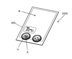
- FIG. 1 is a perspective view of the display device 2000
- FIG. 2 is an exploded perspective view of the display device 2000.
- An example of the display device 2000 includes, for example, a touch panel.
- the display device 2000 includes a cover member 51, an electrode substrate 52, and a display 400. Below the display 400, a controller 500 (see FIG. 2) is formed.
- the display device 2000 includes an input device 1000.
- the input device 1000 includes an input unit 100 fixed to the cover member 51 by a fixing member 300 and a detection unit 200 formed on the electrode substrate 52.
- the input device 1000 is configured to allow the light emitted upward from the display 400 disposed below the detection unit 200 (details will be described later) to pass through the input unit 100 and the detection unit 200.
- FIG. 3 is a perspective view of the input unit 100.
- FIG. 4 is an exploded perspective view of the input unit 100 as viewed from above.
- FIG. 5 is an exploded perspective view of the input unit 100 as viewed from below.
- the input device 1000 includes the input unit 100 and the detection unit 200, and the detection unit 200 is disposed below the input unit 100.
- the detection unit 200 will be described later with reference to FIG.
- the input unit 100 has a rotating portion 11, a pressing member 12 and a guide portion 13.
- the rotating unit 11 is rotated by the application of a force, for example, by a user, a robot, or a mechanism.
- the pressing member 12 is disposed inside the outer edge of the rotating portion 11. Further, as shown in FIG. 4, the pressing member 12 is composed of a main body portion 12 a, a holding portion 12 b, and a pressing portion 12 c, and at least the main body portion 12 a can transmit light.
- the rotary electrode unit 20 is disposed below the rotary unit 11, and the rotary electrode unit 26 (see FIG. 5) is formed on the rotary electrode unit 20 so as to be exposed to the lower surface.
- the rotating electrode body 26 (see FIG. 5) is rotated by the rotation of the rotating portion 11.
- the metal is insert-formed on the lower surface of the rotary electrode portion 20 which is entirely made of resin so as to be exposed from the resin.
- the portion where metal is exposed corresponds to the rotary electrode body 26, and the remaining portion is the resin 25b.
- the rotary electrode unit 20 is disposed on the holding member 31, and the holding electrode unit 30, the reference electrode unit 60, and the pressing electrode unit 80 are disposed below the holding member 31. That is, the holding electrode body 32 (the holding electrode portion 30) is disposed to face the rotary electrode body 26 via the holding member 31. Then, due to the rotation of the rotary electrode unit 20, the electrical state between the holding electrode body 32 and the rotary electrode body 26 changes.
- FIG. 6 is a schematic view of a detection unit 200 of the present disclosure.
- FIG. 7 is a partial cross-sectional view along line YY of the detection unit 200 shown in FIG.
- the detection unit 200 is formed on the electrode substrate 52, and the cover member 51 is stacked on the electrode substrate on which the detection unit 200 is formed.
- the electrode substrate 52 and the cover member 51 are not shown in FIG.
- the detection unit 200 includes a first detection electrode unit 40 located at the periphery and a second detection electrode unit 90 located at the center.
- the first detection electrode unit 40 includes a detection electrode body 41 having a pair of the reception electrode 41a and the transmission electrode 41b, a detection electrode body 42 having a pair of the reception electrode 42a and the transmission electrode 42b, a reception electrode 43a and a transmission electrode 43b And a detection electrode body 43 having a pair.
- Four second detection electrode portions 90 each having the reception electrode 90 a and the transmission electrode 90 b as a pair are formed.
- the receiving electrode 42 a is disposed on the upper surface of the electrode substrate 52
- the transmitting electrode 42 b is disposed on the lower surface of the electrode substrate 52.
- the receiving electrode 42a and the transmitting electrode 42b are opposed in the vertical direction.
- the positional relationship between the receiving electrode 42a and the transmitting electrode 42b has been described here, the positional relationship between the receiving electrode 41a and the transmitting electrode 41b and the positional relationship between the receiving electrode 43a and the transmitting electrode 43b are the same.
- FIG. 8 is a schematic view for explaining a cross section of the display device shown in FIG.
- a detection unit 200 is disposed below the input unit 100.
- the detection unit 200 is only schematically shown, and for example, the transmission electrodes 42 b and 43 b are not illustrated.
- the detection electrode body 42 (see FIG. 6) is located below the pressing electrode portion 80 (see FIG. 4), and the detection electrode bodies 41 and 42 (FIG. 6) under the two holding electrode bodies 32 (see FIG. 4). See) is located.
- the reception electrode unit 44 (see FIG. 6) is located below the reference electrode unit 60 (see FIG. 4).
- the reception electrode 41a and the transmission electrode 41b are capacitively coupled, and the rotation of the rotation unit 11 causes the reception electrode 41a and the transmission electrode 41b (or the reception electrode 42a and the transmission electrode 42b) And the capacitance between them changes.
- the first detection electrode unit 40 (the reception electrode 41 a, the transmission electrode 41 b, the reception electrode 42 a, the transmission electrode 42 b, the reception electrode 43 a, the transmission electrode 43 b, the reception electrode unit 44) is formed in the substrate unit 50. It is done.
- the substrate unit 50 transmits light in a region (first region A) opposed to the main body 12a (transmission portion) of the pressing member 12 (see FIG. 8).
- the input device 1000 includes the pressing member 12 disposed inside the outer edge of the rotating portion 11 and transmitting light, and the substrate portion 50 transmitting light in the first region A facing the pressing member 12.
- the substrate unit 50 is configured of the cover member 51 and the electrode substrate 52. With this configuration, light that has entered the first region A from below the substrate unit 50 can pass through the substrate unit 50 and the pressing member 12 and travel upward from the pressing member 12. Therefore, the input device 1000 can visually recognize an object located below the substrate unit 50 through the pressing member 12 and the substrate unit 50.
- the input device 1000 includes an input unit 100 and a detection unit 200. As described above, the input device 1000 is configured to be able to transmit light incident from below the detection unit 200 to the upper side of the input unit 100. Further, the input device 1000 receives mechanical input by the input unit 100. Here, mechanical input includes, for example, rotation, pushing, pulling, and sliding. Then, the detection unit 200 converts at least one input of the inputs input to the input unit 100 into a change in capacitance.
- FIG. 4 is an exploded perspective view of the input unit 100 shown in FIG. 3 as viewed from above.
- FIG. 5 is an exploded perspective view of the input unit 100 shown in FIG. 3 as viewed from below.
- the input unit 100 includes a rotating portion 11, a rotating electrode portion 20 including a rotating electrode body 26, a holding electrode portion 30 including two holding electrode bodies 32, a reference electrode portion 60, a switch body 70, and a pressing electrode portion And 80.
- the input unit 100 has a rotating portion 11, a pressing member 12 and a guide portion 13.
- the rotating portion 11 is formed in an annular shape having a circular outer edge and a circular inner edge.
- the rotating portion 11 is rotatably held by the holding member 31.
- the pressing member 12 and the guide portion 13 are disposed inside the inner edge of the rotating portion 11.
- the ring shape of the rotating portion 11 may be a polygon. For example, it may be annular with the outer edge of the polygon and the inner edge of the polygon. In addition, in the ring shape of the rotating portion 11, the shape of the inner edge and the shape of the outer edge do not have to match.
- the ring shape of the rotating portion 11 may be an annular shape having a polygonal outer edge and a circular inner edge, or may be an annular shape having a circular outer edge and a polygonal inner edge.
- the inner edge and the outer edge of the rotating portion 11 do not have to be strictly circular or polygonal, respectively, and may be annularly formed by a combination of curves and straight lines.
- the inner edge and the outer edge of the rotating portion 11 may have an oval shape, an approximate circle, or an approximate polygon obtained by rounding the corners of a polygon with a curve.
- the rotating portion 11 may have an opening.
- the pressing member 12 has a main body portion 12a, a holding portion 12b, and a pressing portion 12c.
- the body portion 12a is transparent, for example, containing glass, polycarbonate, polystyrene, acrylic or the like, and can transmit light.
- the main body portion 12 a is disposed inside the inner edge of the rotating portion 11. That is, the opening of the rotating portion 11 and the pressing portion 12c overlap in a plan view.
- the main body portion 12 a is located inside the inner edge of the rotating portion 11 and exposed outward from the input device 1000. In other words, the main body 12 a is exposed to the outside from the input device 1000 inside the inner edge of the guide 13.
- the term "transparent” may be colored or transparent. Further, the main body 12a may be transparent as long as visible light incident from below can be viewed from above. Therefore, the main body 12a may be formed to reflect light from above but transmit light from below. That is, the main body 12a may be, for example, a magic mirror.
- the pressing portion 12c protrudes from the main body portion 12a.
- the pressing portion 12 c is disposed above the switch body 70.
- the guide part 13 is arrange
- the pressing portion 12c may be made of the same material as the main portion 12a.
- the pressing portion 12c may be transparent or opaque.
- the pressing portion 12c may be integral with or separate from the main body 12a.
- the holding portion 12 b protrudes from the main body portion 12 a. And the holding part 12b is arrange
- the holding portion 12 b is held between the upper surface of the holding member 31 and the lower surface of the guide portion 13. Further, the holding portion 12 b is held so that the pressing portion 12 c can move up and down.
- the holding portion 12b may be made of the same material as the main portion 12a or the pressing portion 12c.
- the holding portion 12b may be transparent or opaque. Further, the holding portion 12b may be integral with or separate from the main body portion 12a.
- the guide portion 13 is disposed in the ring of the rotating portion 11. Moreover, the guide part 13 is arrange
- the rotary electrode unit 20 has a rotary unit 25 and a rotary electrode body 26 (first electrode body).
- the rotating portion 25 is formed in an annular and cylindrical shape.
- the rotating portion 25 is formed of an insulating resin. Further, on the upper surface of the rotating portion 25, an uneven portion 25 a having a plurality of concave portions and a plurality of convex portions is formed.
- the rotary unit 25 holds the rotary electrode 26 on the lower surface.
- the rotary electrode body 26 has an outer peripheral portion 26a (see FIG. 5) in which notches are formed at equal intervals, and an inner peripheral portion 26b (see FIG. 5) positioned closer to the inner edge of the rotary electrode portion 20 than the outer peripheral portion 26a. , And an annular conductor. Therefore, at the cut position of the rotary electrode body 26, the rotary portion 25 is exposed, and the exposed portion of the rotary portion 25 is shown as the resin 25b.
- the holding electrode unit 30 has a holding member 31, a holding electrode body 32, and a click spring 33.
- the holding member 31 is formed in an annular and cylindrical shape. Further, the holding member 31 is formed with a plurality of holes penetrating from the lower surface to the upper surface.
- the holding member 31 rotatably holds the rotating unit 25.
- the holding member 31 holds the holding electrode body 32 on the lower surface.
- the holding electrode body 32 is disposed at a position facing the rotating electrode body 26. Further, one holding electrode body 32 has a brush 32a and a main body portion 32c, and the other holding electrode body 32 has a brush 32b and a main body portion 32d.
- the brush 32a and the main body 32c are integrally formed of a conductor. Further, the brush 32b and the main body 32d are integrally formed of a conductor.
- the brush 32a and the brush 32b protrude upward through different holes of the corresponding holding member 31, and contact the outer peripheral portion 26a or the rotating portion 25 (resin 25b) of the rotary electrode body 26.
- the main body 32 c and the main body 32 d are held by the lower surface of the holding member 31.
- the click spring 33 has a contact pressure portion 33a.
- the click spring 33 is an annular metal body, and the contact pressure portion 33a has elasticity.
- the click spring 33 is held by the holding member 31 so as to bring the contact portion 33a into contact with the uneven portion 25a.
- the reference electrode unit 60 has a brush 60a and a main body 60b.
- the brush 60a and the main body 60b are integrally formed of a conductor.
- the reference electrode portion 60 is held on the lower surface of the holding member 31.
- the brush 60 a protrudes upward through the hole of the holding member 31 at a position different from the brush 32 a and the brush 32 b and contacts the inner circumferential portion 26 b of the rotary electrode 26.
- the switch body 70 is located below the guide portion 13.
- the switch body 70 is disposed on the holding member 31 and is disposed below the pressing portion 12 c of the pressing member 12. That is, the switch body 70 is sandwiched by the holding member 31 and the pressing portion 12 c.
- the switch body 70 has a first terminal and a second terminal. The first terminal and the second terminal are electrically connected by applying a pressing force. Then, the first terminal of the switch body 70 is electrically connected to the reference electrode unit 60.
- the switch body 70 preferably uses an electronic component that reduces the resistance value by receiving a pressing force.
- an electronic component a push switch, a pressure sensor, a membrane switch etc. are mentioned, for example.
- a click feeling can be generated by pressing the switch body 70.
- a pressure sensor is used as the switch body 70
- an electrical signal can be output according to the pressing force applied to the switch body 70.
- the membrane switch is used as the switch body 70, the amount of movement of the pressing member 12 in the vertical direction can be suppressed.
- the pressing electrode portion 80 is a conductor held on the lower surface of the holding member 31. Further, the pressing electrode unit 80 is disposed at a position between the reference electrode unit 60 and the holding electrode body 32 in the rotational direction. The pressing electrode unit 80 is electrically connected to the second terminal of the switch body 70. Therefore, the press electrode unit 80 is electrically conducted to the reference electrode unit 60 through the switch body 70 in a state where the first terminal and the second terminal of the switch body are electrically conducted.
- FIG. 6 is a schematic view of the detection unit 200.
- FIG. 7 is a cross-sectional view taken along line YY shown in FIG.
- FIG. 8 is a schematic view illustrating the cross section of the display device of the input device 1000. As shown in FIG. The portion of the input unit 100 corresponds to the cross-sectional view along the line XX shown in FIG.
- the detection unit 200 has a first detection electrode unit 40 and a second detection electrode unit 90.
- the first detection electrode unit 40 and the second detection electrode unit 90 are formed on the electrode substrate 52 (see FIG. 8).
- the capacitance is changed by the operation of the input unit 100.
- the first detection electrode unit 40 includes a detection electrode body 41, a detection electrode body 42, a detection electrode body 43, and a reception electrode portion 44.
- the detection electrode body 41 has a reception electrode 41a and a transmission electrode 41b.
- the receiving electrode 41a and the transmitting electrode 41b are electrodes having conductivity.
- the receiving electrode 41a is electrically insulated from the transmitting electrode 41b. Further, the receiving electrode 41a is formed in an annular shape, and is disposed above the transmitting electrode 41b. Furthermore, between the receiving electrode 41a and the transmitting electrode 41b, for example, an insulating layer such as air, resin, or glass is disposed. In the input device 1000, the insulating layer is borne by an electrode substrate 52 described later. That is, the electrode substrate 52 is disposed between the reception electrode 41a and the transmission electrode 41b. Then, the capacitance between the transmission electrode 41 b and the reception electrode 41 a is changed by the rotation of the rotation unit 11 of the input unit 100.
- the detection electrode body 42 has a reception electrode 42 a and a transmission electrode 42 b.
- the receiving electrode 42 a and the transmitting electrode 42 b are electrodes having conductivity.
- the receiving electrode 42a is electrically insulated from the transmitting electrode 42b.
- the receiving electrode 42a is formed in an annular shape, and is disposed above the transmitting electrode 42b.
- an insulating layer such as air, resin, or glass is disposed between the input device 1000.
- the insulating layer is borne by an electrode substrate 52 described later. That is, the electrode substrate 52 is disposed between the receiving electrode 42a and the transmitting electrode 42b.
- the electrostatic capacitance between the transmission electrode 42 b and the reception electrode 42 a is changed by the rotation of the rotation unit 11 of the input unit 100.
- the detection electrode body 43 has a reception electrode 43a and a transmission electrode 43b.
- the receiving electrode 42 a and the transmitting electrode 42 b are electrodes having conductivity.
- the receiving electrode 43a is electrically insulated from the transmitting electrode 43b. Further, the receiving electrode 43a is annularly formed, and is disposed above the transmitting electrode 43b. Furthermore, between the receiving electrode 43a and the transmitting electrode 43b, for example, an insulating layer such as air, resin, or glass is disposed. In the input device 1000, the insulating layer is borne by an electrode substrate 52 described later. That is, the electrode substrate 52 is disposed between the reception electrode 43a and the transmission electrode 43b.
- the electrostatic capacitance between the transmission electrode 43 b and the reception electrode 43 a changes when the switch body 70 is pressed.
- the switch body 70 is pressed by the pressing portion 12 c when the pressing member 12 is pressed. That is, the electrostatic capacitance between the transmission electrode 43 b and the reception electrode 43 a changes when the pressing member 12 is pressed.
- the reception electrode unit 44 is a reference of detection of the detection electrode body 41, the detection electrode body 42, and the detection electrode body 43.
- the receiving electrode unit 44 is a conductive electrode disposed at a position facing the reference electrode unit 60 (see FIG. 4).
- the receiving electrode unit 44 is electrically connected to the ground and has a ground potential.
- the first detection electrode unit 40 is configured to detect the rotation and the pressing by the electrically independent electrodes (the detection electrode body 41 or the detection electrode body 42 and the detection electrode body 43). Thereby, the erroneous detection of rotation or a press can be suppressed. Further, by having the detection electrode body 41 and the detection electrode body 42, the first detection electrode unit 40 can output an electrical signal according to the rotation direction of the rotation unit 11. Therefore, when outputting that the rotation unit 11 is rotating as an electric signal, the first detection electrode unit 40 may have either the detection electrode body 41 or the detection electrode body 42.
- the reception electrodes 41a, 42a, 43a and the transmission electrodes 41b, 42b, 43b may be metal electrodes containing metals such as copper, silver, aluminum, gold and the like, and conductive metal oxides such as ITO (Indium Tin Oxide).
- a transparent electrode including a conductive material, a conductive organic material, or a carbon material such as graphene may be used.
- the substrate unit 50 has a cover member 51 and an electrode substrate 52.
- the cover member 51 has a first surface and a second surface.
- the first surface of the cover member 51 faces the holding electrode unit 30.
- the second surface is the back surface of the first surface, and is located below the second surface.
- the cover member 51 has a hardness higher than or equal to that of the electrode substrate 52 and has translucency in at least a first region A facing the main body 12 a of the pressing member 12.
- the electrode substrate 52 is, for example, a film having a hardness similar to that of the cover member 51 or a hardness lower than that of the electrode substrate 52, and has translucency in at least the first region A facing the main body 12a of the pressing member 12.
- the substrate unit 50 is configured to allow light to pass from the lower surface to the upper surface at least in the first region A.
- Receiving electrodes 41 a, 42 a and 43 a are formed on the top surface of the electrode substrate 52.
- transmission electrodes 41 b, 42 b and 43 b are formed on the lower surface of the electrode substrate 52.
- the electrode substrate 52 may be formed by overlapping a plurality of films, or may be a single film. In the case of a plurality of films, the receiving electrodes 41a, 42a and 43a may not be formed on the uppermost surface, and the transmitting electrodes 41b, 42b and 43b may not be formed on the lowermost surface.
- the capacitance of the second detection electrode unit 90 changes as the object contacts or approaches the pressing member 12.
- examples of the object include human fingers and robot arms.
- the second detection electrode unit 90 is formed in a first region A of the electrode substrate 52 facing the main body 12 a of the pressing member 12.
- the second detection electrode unit 90 has light transparency.
- the second detection electrode unit 90 is formed on the same plane as the first detection electrode unit 40, but may be formed on a plane different from the first detection electrode unit 40.
- the second detection electrode unit 90 has four electrically independent electrodes and is arranged in a cross shape. Each of the four electrodes of the second detection electrode unit has a reception electrode 90 a and a transmission electrode 90 b, and is disposed on the electrode substrate 52.
- the receiving electrode 90a is annularly formed, and is disposed above the transmitting electrode 90b. That is, the electrode substrate 52 is disposed as an insulating layer between the reception electrode 90a and the transmission electrode 90b.
- the electrostatic capacitance between the receiving electrode 90 a and the transmitting electrode 90 b is changed by the contact or proximity of the object to the pressing member 12.
- the degree of light transmission of the second detection electrode unit 90 is transparent to such an extent that light incident from below the electrode substrate 52 can enter the pressing member 12 in a state where the second detection electrode unit 90 is formed on the electrode substrate 52
- the second detection electrode unit 90 may use a metal electrode containing a metal such as copper, silver, aluminum, or gold as long as the above-described light transmittance can be satisfied, and the conductive property such as ITO (Indium Tin Oxide)
- ITO Indium Tin Oxide
- a transparent electrode including a metal oxide, a conductive organic material, or a carbon material such as graphene may be used.
- a thin wire is formed of metal
- a thin wire is formed of metal in a mesh shape
- a thin wire formed of metal is blackened, or the metal electrode is formed in any direction. Is preferred.
- the rotating unit 25 is rotated by the rotation of the rotating unit 11.
- the rotating electrode body 26 is held on the lower surface of the rotating portion 25 (see FIG. 5). Therefore, the rotating electrode body 26 rotates with the rotating portion 11.
- the rotary electrode body 26 is in contact with the brush 60 a (see FIG. 4) of the reference electrode unit 60 at the inner circumferential portion 26 b.
- the rotary electrode body 26 contacts the brush 32 a and the brush 32 b of the holding electrode body 32 at the outer peripheral portion 26 a of the rotary electrode body 26.
- the receiving electrode 41a faces the main body 32d. Therefore, the capacitance between the reception electrode 41a and the transmission electrode 41b changes due to the change in the electrical state of the main body 32d.
- the receiving electrode 42a faces the main body 32c. Therefore, the capacitance between the receiving electrode 42a and the transmitting electrode 42b changes due to a change in the electrical state of the main body 32c.
- the change in electrical state between the main body 60b and the main body 32c is different from the change in electrical state between the main body 60b and the main body 32d. Therefore, the capacitance change between the reception electrode 42a and the transmission electrode 42b is different from the capacitance change between the reception electrode 41a and the transmission electrode 41b.
- the pressing member 12 presses the switch body 70 with the pressing portion 12 c by being pressed downward.
- the reference electrode portion 60 and the pressing electrode portion 80 are electrically connected. That is, the reference electrode unit 60 and the pressing electrode unit 80 are in a conductive state when the pressing member 12 is pressed, and are in a disconnected state when the pressing member 12 is not pressed.
- the receiving electrode 43 a faces the pressing electrode unit 80. Therefore, the capacitance between the receiving electrode 43a and the transmitting electrode 43b changes due to the change in the electrical state of the pressing electrode unit 80.
- the input device 1000 can rotate the rotating unit 11, press the pressing member 12, approach or contact an object to the pressing member 12, to set the static state between the reception electrode and the transmission electrode corresponding to each operation. Change in capacitance. Thereby, the input device 1000 can output these electrostatic capacitance changes as an electrical signal.
- the input device 1000 light is transmitted through at least a first region A (see FIG. 8) of the substrate unit 50 facing the main body 12a of the pressing member 12. Therefore, when the pressing member 12 is viewed from above the pressing member 12, the portion below the substrate unit 50 can be viewed.
- the input device 1000 also has a second detection electrode unit 90 at a position facing the pressing member 12. Further, the second detection electrode unit 90 is formed to be able to transmit light. Therefore, the input device 1000 can perform touch input and hover input with the pressing member 12 while looking at an object located below the substrate unit 50.
- the input device 1000 is configured to conduct the reference electrode unit 60 and the pressing electrode unit 80 by pressing the pressing member 12 downward, and to change the capacitance of the first detection electrode unit 40. Therefore, the input device 1000 can realize the pressing input in addition to the rotation input while looking at the lower side of the substrate unit 50.
- the input device 1000 forms the detection electrode body 41 or the detection electrode body 42 on the same plane as the detection electrode body 43, there is no need to provide a separate circuit board for detecting a pressure. It is possible to realize miniaturization and thinning.
- the switch body 70 which brings the reference electrode portion 60 and the pressing electrode portion 80 into conduction by pressing is disposed at a position close to the outer edge of the pressing member 12.
- the switch body 70 is disposed at a position closer to the rotating portion 11 than the main body portion 12 a visible from above the input device 1000. Therefore, when the input device 1000 views the pressing member 12 from above the pressing member 12, the switch body 70 can be prevented from blocking the lower side than the substrate unit 50, so that the visibility can be improved.
- FIG. 8 is a schematic diagram for explaining a cross section of the display device 2000.
- FIG. 9 is a diagram for explaining the operation of the display device 2000.
- 10 and 11 are diagrams for explaining the operation of the display device.
- the display device 2000 includes an input device 1000, a display 400, and a controller 500.
- the input device 1000 includes an input unit 100, a detection unit 200, and a fixing member 300.
- the substrate unit 50 of the detection unit 200 is configured of a transparent touch panel having a cover member 51.
- the substrate unit 50 is formed larger than the input unit 100. That is, the input device 1000 can transmit light by the pressing member 12 and the second area B outside the input unit 100.
- the fixing member 300 is disposed between the input unit 100 and the detection unit 200, and holds the input unit 100 and the detection unit 200.
- the detection unit 200 is electrically connected to the controller 500.
- the display 400 is configured of, for example, a liquid crystal display, an organic electroluminescence (organic EL) display, a transparent display, or the like.
- the display 400 is disposed below the input device 1000. Therefore, the content displayed on the display 400 can be viewed from above the display device 2000 in the first area A and the second area B.
- the displays 400 located at positions corresponding to the first area A and the second area B may be the same display or separate displays.
- the display 400 is electrically connected to the controller 500.
- the controller 500 is electrically connected to the detection unit 200 and the display 400.
- the controller 500 detects the capacitance change in the detection unit 200 to determine the input (rotation, press, touch or approach) received by the input unit 100. Then, the controller 500 controls the content displayed on the display 400 according to the input content.
- FIGS. 9 to 11. 10 and 11 are diagrams for explaining the operation of the display device 2000.
- the controller 500 in the first area A causes the operator to The selected "Temp” is displayed in the second area B.
- controller 500 determines that the content selected by the operator has been determined, and changes the content displayed in first area A and second area B. (See Figure 11).
- the controller 500 changes the display 400 to a temperature setting screen.
- the temperature setting screen in the first area A, the relationship between the rotational direction of the rotating portion 11 and the temperature rise and fall is displayed, and in the second area B, the current set temperature is displayed. Then, the operator can change the temperature setting by rotating the rotating unit 11.
- the display region is divided into the first region A and the second region B of the input device 1000. Then, the controller 500 controls the content displayed in the first area A and the second area B. Therefore, the operator can operate the display device 2000 more easily.
- the controller 500 may display the same content as the content selected in the first region A in the second region B, and the content based on the content selected in the first region A is the second region B. It may be displayed on the screen. For example, a folder may be displayed in the first area A, and the contents of the selected folder may be displayed in the second area B. Further, for example, an icon may be displayed in the first area A, and a description on the selected icon may be displayed in the second area B.
- the input device 1000 is disposed so as to overlap the rotating portion 11 having the opening with the opening of the rotating portion 11 in plan view, and transmits light in the first region A overlapping in plan view with the opening.
- a rotating electrode unit 20 having a first electrode body (rotating electrode body 26) and a second electrode body (holding electrode body 32).
- the brush 32 a / the brush 32 b) of the two-electrode assembly (holding electrode assembly 32) is disposed to face the rotating electrode unit 20, and the second electrode assembly (holding A holding electrode unit 30 in which the electrode body 32) is in contact with and separated from the first electrode body (rotating electrode body 26), a first detection electrode unit 40 arranged to face the holding electrode unit 30, and a first detection electrode unit And a substrate unit 50 on which 40 is formed.
- the 1st sensing electrode part 40 is the 1st receiving electrode (receiving electrode 41a / receiving electrode 42a) arranged so that it may overlap with the 2nd electrode body (holding electrode body 32) in plane view, and the 1st in plane view.
- the capacitance between the first transmission electrode (the transmission electrode 41 b / the transmission electrode 42 b) changes with the rotation of the rotary electrode unit 20, and in the first region A, through the substrate unit 50 and the pressing member 12. Light is transmitted.
- a reference electrode unit 60 electrically connected to the holding electrode unit 30 through the rotary electrode unit 20, and a first surface opposite to the first surface where the substrate unit 50 faces the holding electrode unit 30.
- a pressing electrode unit 80 which is electrically connected to the reference electrode unit 60 by pressing the pressing member 12 in a first direction (direction from the top to the bottom) directed to the side second surface.
- the first detection electrode unit 40 is disposed so as to overlap the second reception electrode (reception electrode 43a) disposed so as to overlap the pressing electrode unit 80 in a plan view and the second reception electrode (reception electrode 43a) in a plan view And a second transmission electrode (transmission electrode 43b).
- the capacitance between the second reception electrode (reception electrode 43a) and the second transmission electrode (transmission electrode 43b) changes as the pressing member 12 is pressed downward.
- the input device 1000 of the present disclosure further includes a switch body 70 that electrically connects the reference electrode unit 60 to the pressing electrode unit 80 by pressing the pressing member 12 downward.
- the pressing member 12 has a main body portion 12 a that transmits light, and a pressing portion 12 c that protrudes from the main body portion 12 a.
- the switch body 70 is disposed below the pressing portion 12 c of the pressing member 12.
- the input device 1000 of the present disclosure further includes a second detection electrode unit 90 disposed on the substrate unit 50 so as to overlap with the pressing unit 12 c of the pressing member 12 in a plan view.
- the second detection electrode unit 90 detects whether an object (for example, a finger C) contacts or approaches the pressing unit 12c.
- the input device according to the present disclosure has an effect of transmitting light incident from the first direction more than the input device in the second direction more than the input device, and is useful when used in various electronic devices and the like.
Abstract
This input device is provided with: a rotary part that has an opening; a pressing member that transmits light in a first region; a rotary electrode part that has a first electrode body; a holding electrode part which has a second electrode body and in which the second electrode body is brought into contact with and separated from the first electrode body by means of rotation of the rotary electrode part; a first detection electrode part that is disposed so as to face the holding electrode part; and a substrate part on which the first detection electrode part is formed. In the first region, light transmits through the substrate part and the pressing member.
Description
本開示は、各種電子機器への入力に用いられる入力装置に関する。
The present disclosure relates to an input device used for input to various electronic devices.
従来の入力装置は、入力ユニットと検出ユニットとを有する。
A conventional input device comprises an input unit and a detection unit.
入力ユニットは、入力部と、回転電極部と、保持電極部とを有する。入力部は、回転する回転部を含む。回転電極部は、回転部の回転によって回転する。保持電極部は、回転電極部と向かい合う位置に配置されている。そして、保持電極部は、回転電極部の回転によって回転電極部との間の電気的な状態が変化する。
The input unit includes an input unit, a rotating electrode unit, and a holding electrode unit. The input unit includes a rotating unit that rotates. The rotating electrode unit is rotated by the rotation of the rotating unit. The holding electrode unit is disposed at a position facing the rotating electrode unit. The holding electrode unit changes its electrical state with the rotating electrode unit by the rotation of the rotating electrode unit.
検出ユニットは、第1検出電極部と、基板部とを有する。基板部は、電子部品が配置されており、電子回路を有する。また、基板部は、電子回路が形成された面の反対側の面に、第1検出電極部が形成されている。第1検出電極部は、保持電極部と向かい合う位置に配置されている。第1検出電極部は、回転部の回転によって静電容量が変化する。
The detection unit has a first detection electrode unit and a substrate unit. The substrate portion is provided with electronic components and has an electronic circuit. Further, in the substrate portion, the first detection electrode portion is formed on the surface opposite to the surface on which the electronic circuit is formed. The first detection electrode unit is disposed at a position facing the holding electrode unit. The capacitance of the first detection electrode unit changes due to the rotation of the rotation unit.
このような従来の入力装置として、たとえば、特許文献1に開示の入力装置が知られている。
As such a conventional input device, for example, an input device disclosed in Patent Document 1 is known.
本開示の一態様の入力装置は、開口部を有する回転部と、平面視で、前記回転部の前記開口部と重なるように配置され、前記開口部と前記平面視で重なる第1領域内において光を透過する押圧部材と、前記回転部の回転に応じて回転し、第1電極体を有する回転電極部と、第2電極体を有し、前記第2電極体の少なくとも一部が前記回転電極部と対向するように配置され、前記回転電極部の回転によって、前記第2電極体が前記第1電極体と接離する保持電極部と、前記保持電極部に対向するように配置される第1検出電極部と、前記第1検出電極部が形成される基板部と、を備え、前記第1検出電極部は、前記平面視で前記第2電極体と重なるように配置される第1受信電極と、前記平面視で前記第1受信電極と重なるように配置される第1送信電極と、を有し、前記第1受信電極と前記第1送信電極との間の静電容量は、前記回転電極部の回転によって変化し、前記第1領域内において、前記基板部および前記押圧部材を介して光が透過する。
The input device according to one aspect of the present disclosure is disposed in a first region that is disposed so as to overlap the rotating portion having an opening and the opening of the rotating portion in a plan view and overlaps the opening in the plan view. It has a pressing member which transmits light, a rotating electrode unit having a first electrode body which rotates according to the rotation of the rotating unit, and a second electrode body, and at least a part of the second electrode body is the rotation The second electrode body is disposed so as to face the electrode portion, and the second electrode body is disposed so as to face the holding electrode portion, the holding electrode portion coming into contact with and separated from the first electrode body by rotation of the rotary electrode portion. A first detection electrode portion and a substrate portion on which the first detection electrode portion is formed, the first detection electrode portion being disposed so as to overlap the second electrode body in the plan view. The receiving electrode is disposed to overlap the first receiving electrode in the plan view. A capacitance between the first receiving electrode and the first transmitting electrode is changed by the rotation of the rotating electrode portion, and the substrate portion and the first transmitting electrode in the first region Light is transmitted through the pressing member.
この構成により、本開示の入力装置は、第1領域内において、第1の方向から入射した光を前記第1の方向と反対の第2の方向へと透過できる。
With this configuration, the input device of the present disclosure can transmit light incident from a first direction in a second direction opposite to the first direction in the first region.
今般、入力装置よりも第1の方向(下方)にディスプレイを配置し、第1の方向とは逆の方向である第2の方向(上方)から入力装置を見た場合に、入力装置を介してディスプレイに表示される内容等を視認できるような表示装置が求められている。
At this time, when the display is disposed in the first direction (lower side) than the input device, and the input device is viewed from the second direction (upper side) which is the direction opposite to the first direction, There is a need for a display device that allows the user to visually recognize the content etc. displayed on the display.
上述した従来の入力装置では、電子部品と第1検出電極部とを同一の基板部に配置するために、プリント基板などの不透明な基板を基板部に用いている。そのため、入力装置よりも第1の方向(下方)から入力装置へ入射した光は、入力装置よりも第2の方向(上方)へと透過しにくかった。
In the above-described conventional input device, in order to arrange the electronic component and the first detection electrode unit on the same substrate unit, an opaque substrate such as a printed circuit board is used for the substrate unit. Therefore, light incident on the input device from the first direction (lower side) than the input device was less likely to transmit in the second direction (upper direction) than the input device.
なお、本開示では、理解し易いよう、第1の方向を「下」とし、第2の方向を「上」として説明する。
In the present disclosure, for the sake of easy understanding, the first direction will be described as “down” and the second direction will be described as “upper”.
つまり、ユーザが上方から入力装置を見た時、入力装置の下方に位置するディスプレイの表示を視認できる入力装置が求められている。言い換えると、下方から入力装置に入射した光を入力装置よりも上方へと透過できるような入力装置が求められている。
That is, there is a need for an input device that can visually recognize the display on the display located below the input device when the user looks at the input device from above. In other words, there is a need for an input device that can transmit light incident on the input device from below to the upper side of the input device.
なお、第1の方向を「下」とし、第2の方向を「上」として説明するが、「第1の方向」と「第2の方向」は、互いに逆向きの方向であればよい。
Although the first direction is described as “down” and the second direction is described as “upper”, the “first direction” and the “second direction” may be directions opposite to each other.
本開示では、「上」、「下」、「右」、「左」、「上方」、「下方」等の方向を示す用語を用いて説明するが、これらは相対的な位置関係を示しているだけであり、それにより本開示が限定されるものではない。
Although the present disclosure will be described using terms indicating directions such as “upper,” “lower,” “right,” “left,” “upper,” “lower,” etc., these indicate relative positional relationships. However, the present disclosure is not limited thereby.
(実施の形態)
[表示装置2000の概要]
図1および図2を参照ながら表示装置2000の構成について説明する。図1は表示装置2000の斜視図であり、図2は表示装置2000の展開斜視図である。表示装置2000の例として、例えばタッチパネルが挙げられる。表示装置2000は、カバー部材51、電極基板52、ディスプレイ400を有する。ディスプレイ400の下方には、コントローラ500(図2参照)が形成されている。表示装置2000は、入力装置1000を備えている。入力装置1000は、固定部材300によってカバー部材51に固定されている入力ユニット100と、電極基板52に形成される検出ユニット200と、を有する。入力装置1000は、検出ユニット200(詳細は後述する)の下方に配置されているディスプレイ400から上方に向かって発する光を入力ユニット100および検出ユニット200を透過できるように構成されている。 Embodiment
[Overview of Display Device 2000]
The configuration of thedisplay device 2000 will be described with reference to FIGS. 1 and 2. FIG. 1 is a perspective view of the display device 2000, and FIG. 2 is an exploded perspective view of the display device 2000. An example of the display device 2000 includes, for example, a touch panel. The display device 2000 includes a cover member 51, an electrode substrate 52, and a display 400. Below the display 400, a controller 500 (see FIG. 2) is formed. The display device 2000 includes an input device 1000. The input device 1000 includes an input unit 100 fixed to the cover member 51 by a fixing member 300 and a detection unit 200 formed on the electrode substrate 52. The input device 1000 is configured to allow the light emitted upward from the display 400 disposed below the detection unit 200 (details will be described later) to pass through the input unit 100 and the detection unit 200.
[表示装置2000の概要]
図1および図2を参照ながら表示装置2000の構成について説明する。図1は表示装置2000の斜視図であり、図2は表示装置2000の展開斜視図である。表示装置2000の例として、例えばタッチパネルが挙げられる。表示装置2000は、カバー部材51、電極基板52、ディスプレイ400を有する。ディスプレイ400の下方には、コントローラ500(図2参照)が形成されている。表示装置2000は、入力装置1000を備えている。入力装置1000は、固定部材300によってカバー部材51に固定されている入力ユニット100と、電極基板52に形成される検出ユニット200と、を有する。入力装置1000は、検出ユニット200(詳細は後述する)の下方に配置されているディスプレイ400から上方に向かって発する光を入力ユニット100および検出ユニット200を透過できるように構成されている。 Embodiment
[Overview of Display Device 2000]
The configuration of the
[入力ユニット100の概要]
図3から図5を参照しながら入力ユニット100について説明する。図3は入力ユニット100の斜視図である。図4は入力ユニット100を上方から見た展開斜視図である。図5は入力ユニット100を下方から見た展開斜視図である。上述した通り、入力装置1000は、入力ユニット100と検出ユニット200を有しており、入力ユニット100の下方には、検出ユニット200が配置される。なお、検出ユニット200については、図6などを参照しながら後述する。 [Overview of Input Unit 100]
Theinput unit 100 will be described with reference to FIGS. 3 to 5. FIG. 3 is a perspective view of the input unit 100. FIG. FIG. 4 is an exploded perspective view of the input unit 100 as viewed from above. FIG. 5 is an exploded perspective view of the input unit 100 as viewed from below. As described above, the input device 1000 includes the input unit 100 and the detection unit 200, and the detection unit 200 is disposed below the input unit 100. The detection unit 200 will be described later with reference to FIG.
図3から図5を参照しながら入力ユニット100について説明する。図3は入力ユニット100の斜視図である。図4は入力ユニット100を上方から見た展開斜視図である。図5は入力ユニット100を下方から見た展開斜視図である。上述した通り、入力装置1000は、入力ユニット100と検出ユニット200を有しており、入力ユニット100の下方には、検出ユニット200が配置される。なお、検出ユニット200については、図6などを参照しながら後述する。 [Overview of Input Unit 100]
The
図3に示すように入力ユニット100は回転部11と押圧部材12とガイド部13とを有する。回転部11は、たとえばユーザ、ロボット、機構などによって力を加えられることにより回転する。押圧部材12は、回転部11の外縁よりも内側に配置されている。また、図4に示すように、押圧部材12は、本体部12a、保持部12b、押圧部12cで構成されており、少なくとも本体部12aは光を透過することができる。
As shown in FIG. 3, the input unit 100 has a rotating portion 11, a pressing member 12 and a guide portion 13. The rotating unit 11 is rotated by the application of a force, for example, by a user, a robot, or a mechanism. The pressing member 12 is disposed inside the outer edge of the rotating portion 11. Further, as shown in FIG. 4, the pressing member 12 is composed of a main body portion 12 a, a holding portion 12 b, and a pressing portion 12 c, and at least the main body portion 12 a can transmit light.
回転部11の下方には回転電極部20が配置されており、回転電極部20には、下面に露出するように回転電極体26(図5参照)が形成されている。回転電極体26(図5参照)は、回転部11の回転によって回動する。
The rotary electrode unit 20 is disposed below the rotary unit 11, and the rotary electrode unit 26 (see FIG. 5) is formed on the rotary electrode unit 20 so as to be exposed to the lower surface. The rotating electrode body 26 (see FIG. 5) is rotated by the rotation of the rotating portion 11.
ここで、回転電極体26の形成方法について、簡単に説明する。全体が樹脂で形成されている回転電極部20の下面に金属を樹脂から露出するようにインサート形成する。その結果、図5に示すように、回転電極部20の下面のうち、金属が露出している部分が回転電極体26に対応し、残りの部分が樹脂25bになる。
Here, a method of forming the rotary electrode 26 will be briefly described. The metal is insert-formed on the lower surface of the rotary electrode portion 20 which is entirely made of resin so as to be exposed from the resin. As a result, as shown in FIG. 5, of the lower surface of the rotary electrode portion 20, the portion where metal is exposed corresponds to the rotary electrode body 26, and the remaining portion is the resin 25b.
回転電極部20は保持部材31の上に配置されており、保持部材31の下方には、保持電極部30、基準電極部60、押圧電極部80が配置されている。つまり、保持電極体32(保持電極部30)は、回転電極体26と保持部材31を介して向かい合うように配置されている。そして、回転電極部20の回転によって、保持電極体32と回転電極体26との間の電気的な状態は変化する。
The rotary electrode unit 20 is disposed on the holding member 31, and the holding electrode unit 30, the reference electrode unit 60, and the pressing electrode unit 80 are disposed below the holding member 31. That is, the holding electrode body 32 (the holding electrode portion 30) is disposed to face the rotary electrode body 26 via the holding member 31. Then, due to the rotation of the rotary electrode unit 20, the electrical state between the holding electrode body 32 and the rotary electrode body 26 changes.
[検出ユニット200の概要]
次に、図6および図7を参照しながら検出ユニット200の概要について説明する。図6は、本開示の検出ユニット200の概略図である。図7は、図6に示す検出ユニット200のY-Y線における部分断面図である。 [Overview of Detection Unit 200]
Next, the outline of thedetection unit 200 will be described with reference to FIGS. 6 and 7. FIG. 6 is a schematic view of a detection unit 200 of the present disclosure. FIG. 7 is a partial cross-sectional view along line YY of the detection unit 200 shown in FIG.
次に、図6および図7を参照しながら検出ユニット200の概要について説明する。図6は、本開示の検出ユニット200の概略図である。図7は、図6に示す検出ユニット200のY-Y線における部分断面図である。 [Overview of Detection Unit 200]
Next, the outline of the
なお、図8などを参照しながら後述するが、検出ユニット200は、電極基板52の上に形成され、検出ユニット200が形成される電極基板の上にはカバー部材51が積層されている。図6には、電極基板52およびカバー部材51は示していない。
Although described later with reference to FIG. 8 and the like, the detection unit 200 is formed on the electrode substrate 52, and the cover member 51 is stacked on the electrode substrate on which the detection unit 200 is formed. The electrode substrate 52 and the cover member 51 are not shown in FIG.
図6に示すように、検出ユニット200は、周辺部に位置する第1検出電極部40と、中央部に位置する第2検出電極部90と、を含む。
As shown in FIG. 6, the detection unit 200 includes a first detection electrode unit 40 located at the periphery and a second detection electrode unit 90 located at the center.
第1検出電極部40は、受信電極41aと送信電極41bとを一対とする検出電極体41、受信電極42aと送信電極42bとを一対とする検出電極体42、受信電極43aと送信電極43bとを一対とする検出電極体43を有する。受信電極90aと送信電極90bとを一対とする第2検出電極部90は、4つ形成されている。
The first detection electrode unit 40 includes a detection electrode body 41 having a pair of the reception electrode 41a and the transmission electrode 41b, a detection electrode body 42 having a pair of the reception electrode 42a and the transmission electrode 42b, a reception electrode 43a and a transmission electrode 43b And a detection electrode body 43 having a pair. Four second detection electrode portions 90 each having the reception electrode 90 a and the transmission electrode 90 b as a pair are formed.
図7に示すように、受信電極42aは電極基板52の上面に配置され、送信電極42bは電極基板52の下面に配置されている。受信電極42aおよび送信電極42bは上下方向に対向している。なお、ここでは、受信電極42aおよび送信電極42bの位置関係について説明したが、受信電極41aおよび送信電極41bの位置関係、受信電極43aおよび送信電極43bの位置関係についても同様である。
As shown in FIG. 7, the receiving electrode 42 a is disposed on the upper surface of the electrode substrate 52, and the transmitting electrode 42 b is disposed on the lower surface of the electrode substrate 52. The receiving electrode 42a and the transmitting electrode 42b are opposed in the vertical direction. Although the positional relationship between the receiving electrode 42a and the transmitting electrode 42b has been described here, the positional relationship between the receiving electrode 41a and the transmitting electrode 41b and the positional relationship between the receiving electrode 43a and the transmitting electrode 43b are the same.
[入力装置1000の構成]
次に、図3~図8を参照しながら入力装置1000の構成について説明する。 [Configuration of Input Device 1000]
Next, the configuration of theinput device 1000 will be described with reference to FIGS. 3 to 8.
次に、図3~図8を参照しながら入力装置1000の構成について説明する。 [Configuration of Input Device 1000]
Next, the configuration of the
図8は、図1に示す表示装置の断面を説明する概略図である。図8に示すように、本開示の入力装置1000は、入力ユニット100の下方に検出ユニット200が配置されている。なお、図8では、特に検出ユニット200については、概略を示しているだけであり、例えば、送信電極42b、43bなどについては図示していない。
FIG. 8 is a schematic view for explaining a cross section of the display device shown in FIG. As shown in FIG. 8, in the input device 1000 of the present disclosure, a detection unit 200 is disposed below the input unit 100. In FIG. 8, particularly, the detection unit 200 is only schematically shown, and for example, the transmission electrodes 42 b and 43 b are not illustrated.
ここで、入力ユニット100における各電極と、検出ユニット200における各電極との位置関係について説明する。
Here, the positional relationship between each electrode in the input unit 100 and each electrode in the detection unit 200 will be described.
押圧電極部80(図4参照)の下方には検出電極体42(図6参照)が位置し、2つの保持電極体32(図4参照)の下方には検出電極体41,42(図6参照)が位置する。基準電極部60(図4参照)の下方には受信電極部44(図6参照)が位置する。
The detection electrode body 42 (see FIG. 6) is located below the pressing electrode portion 80 (see FIG. 4), and the detection electrode bodies 41 and 42 (FIG. 6) under the two holding electrode bodies 32 (see FIG. 4). See) is located. The reception electrode unit 44 (see FIG. 6) is located below the reference electrode unit 60 (see FIG. 4).
受信電極41aと送信電極41b(または受信電極42aと送信電極42b)とは静電容量結合しており、回転部11の回転によって受信電極41aと送信電極41b(または受信電極42aと送信電極42b)との間の静電容量が変化する。
The reception electrode 41a and the transmission electrode 41b (or the reception electrode 42a and the transmission electrode 42b) are capacitively coupled, and the rotation of the rotation unit 11 causes the reception electrode 41a and the transmission electrode 41b (or the reception electrode 42a and the transmission electrode 42b) And the capacitance between them changes.
ここで、電極基板52の構成について詳しく説明する。
Here, the configuration of the electrode substrate 52 will be described in detail.
図8に示すように、第1検出電極部40(受信電極41a、送信電極41b、受信電極42a、送信電極42b、受信電極43a、送信電極43b、受信電極部44)は、基板部50に形成されている。なお、基板部50は、押圧部材12の本体部12a(透過部)と対向する領域(第1領域A)で光を透過する(図8参照)。
As shown in FIG. 8, the first detection electrode unit 40 (the reception electrode 41 a, the transmission electrode 41 b, the reception electrode 42 a, the transmission electrode 42 b, the reception electrode 43 a, the transmission electrode 43 b, the reception electrode unit 44) is formed in the substrate unit 50. It is done. The substrate unit 50 transmits light in a region (first region A) opposed to the main body 12a (transmission portion) of the pressing member 12 (see FIG. 8).
このように、入力装置1000は、回転部11の外縁よりも内側に配置されて光を透過する押圧部材12と、押圧部材12と向かい合う第1領域Aで光を透過する基板部50とを有する。なお、本開示では、基板部50はカバー部材51と電極基板52とで構成されている。この構成により、基板部50よりも下方から第1領域Aへと入射した光は、基板部50および押圧部材12を透過して押圧部材12よりも上方に向かって進むことができる。そのため、入力装置1000は、基板部50よりも下方に位置する物体を押圧部材12および基板部50を介して視認できる。
As described above, the input device 1000 includes the pressing member 12 disposed inside the outer edge of the rotating portion 11 and transmitting light, and the substrate portion 50 transmitting light in the first region A facing the pressing member 12. . In the present disclosure, the substrate unit 50 is configured of the cover member 51 and the electrode substrate 52. With this configuration, light that has entered the first region A from below the substrate unit 50 can pass through the substrate unit 50 and the pressing member 12 and travel upward from the pressing member 12. Therefore, the input device 1000 can visually recognize an object located below the substrate unit 50 through the pressing member 12 and the substrate unit 50.
図1に示すように、入力装置1000は、入力ユニット100と検出ユニット200とを有する。上述した通り、入力装置1000は、検出ユニット200の下方から入射した光を入力ユニット100の上方へと透過できるよう構成されている。また、入力装置1000は、入力ユニット100で機械的な入力を受け付ける。ここで、機械的な入力には、たとえば、回転、押す、引く、スライドなどである。そして、検出ユニット200は、入力ユニット100で入力される入力のうちの少なくとも1つの入力を静電容量の変化に変換する。
As shown in FIG. 1, the input device 1000 includes an input unit 100 and a detection unit 200. As described above, the input device 1000 is configured to be able to transmit light incident from below the detection unit 200 to the upper side of the input unit 100. Further, the input device 1000 receives mechanical input by the input unit 100. Here, mechanical input includes, for example, rotation, pushing, pulling, and sliding. Then, the detection unit 200 converts at least one input of the inputs input to the input unit 100 into a change in capacitance.
[入力ユニット100の構成]
次に入力ユニット100について、図2から図5を参照ながら説明する。図4は、図3に示す入力ユニット100を上方から見た展開斜視図である。図5は、図3に示す入力ユニット100を下方から見た展開斜視図である。入力ユニット100は、回転部11と、回転電極体26を含む回転電極部20と、2つの保持電極体32を含む保持電極部30と、基準電極部60と、スイッチ体70と、押圧電極部80とを有する。入力ユニット100は、回転部11と押圧部材12とガイド部13とを有する。 [Configuration of input unit 100]
Next, theinput unit 100 will be described with reference to FIGS. 2 to 5. FIG. 4 is an exploded perspective view of the input unit 100 shown in FIG. 3 as viewed from above. FIG. 5 is an exploded perspective view of the input unit 100 shown in FIG. 3 as viewed from below. The input unit 100 includes a rotating portion 11, a rotating electrode portion 20 including a rotating electrode body 26, a holding electrode portion 30 including two holding electrode bodies 32, a reference electrode portion 60, a switch body 70, and a pressing electrode portion And 80. The input unit 100 has a rotating portion 11, a pressing member 12 and a guide portion 13.
次に入力ユニット100について、図2から図5を参照ながら説明する。図4は、図3に示す入力ユニット100を上方から見た展開斜視図である。図5は、図3に示す入力ユニット100を下方から見た展開斜視図である。入力ユニット100は、回転部11と、回転電極体26を含む回転電極部20と、2つの保持電極体32を含む保持電極部30と、基準電極部60と、スイッチ体70と、押圧電極部80とを有する。入力ユニット100は、回転部11と押圧部材12とガイド部13とを有する。 [Configuration of input unit 100]
Next, the
回転部11は、円形の外縁と、円形の内縁とを有する環状に形成されている。そして、回転部11は、保持部材31に回転可能に保持されている。そして、回転部11の内縁の内側には、押圧部材12とガイド部13とが配置されている。
The rotating portion 11 is formed in an annular shape having a circular outer edge and a circular inner edge. The rotating portion 11 is rotatably held by the holding member 31. The pressing member 12 and the guide portion 13 are disposed inside the inner edge of the rotating portion 11.
なお、回転部11の環形状は、多角形であってもよい。たとえば、多角形の外縁と多角形の内縁とを有する環状であってもよい。また、回転部11の環形状は、内縁の形状と外縁の形状とが一致していなくてもよい。たとえば、回転部11の環形状は、多角形の外縁と円形の内縁とを有する環状であってもよく、円形の外縁と多角形の内縁とを有する環状であってもよい。また、回転部11の内縁や外縁は、それぞれ厳密に円形や多角形である必要はなく、曲線や直線の組み合わせによって環状に形成されていてもよい。たとえば、回転部11の内縁や外縁は、楕円形や、おおよそ円形、多角形の角を曲線で丸めたおおよそ多角形といった形状であってもよい。回転部11は開口部を有していればよい。
The ring shape of the rotating portion 11 may be a polygon. For example, it may be annular with the outer edge of the polygon and the inner edge of the polygon. In addition, in the ring shape of the rotating portion 11, the shape of the inner edge and the shape of the outer edge do not have to match. For example, the ring shape of the rotating portion 11 may be an annular shape having a polygonal outer edge and a circular inner edge, or may be an annular shape having a circular outer edge and a polygonal inner edge. Further, the inner edge and the outer edge of the rotating portion 11 do not have to be strictly circular or polygonal, respectively, and may be annularly formed by a combination of curves and straight lines. For example, the inner edge and the outer edge of the rotating portion 11 may have an oval shape, an approximate circle, or an approximate polygon obtained by rounding the corners of a polygon with a curve. The rotating portion 11 may have an opening.
押圧部材12は、本体部12aと、保持部12bと、押圧部12cと、を有している。本体部12aは、たとえば、ガラスや、ポリカーボネート、ポリスチレン、アクリルなどを含み透明で、光を透過できる。本体部12aは、回転部11の内縁より内側に配置されている。つまり、回転部11の開口部と押圧部12cは平面視で重なっている。回転部11よりも上方から回転部11の環内をみた場合(回転部11よりも上方の位置から下方を見た場合)に視認可能な位置にある。言い換えれば、本体部12aは、回転部11の内縁よりも内側に位置し、入力装置1000から外側に露出している。また、言い換えれば、本体部12aは、ガイド部13の内縁よりも内側において、入力装置1000から外側に露出している。
The pressing member 12 has a main body portion 12a, a holding portion 12b, and a pressing portion 12c. The body portion 12a is transparent, for example, containing glass, polycarbonate, polystyrene, acrylic or the like, and can transmit light. The main body portion 12 a is disposed inside the inner edge of the rotating portion 11. That is, the opening of the rotating portion 11 and the pressing portion 12c overlap in a plan view. When the inside of the ring of the rotating portion 11 is viewed from above the rotating portion 11 (when viewed from the position above the rotating portion 11), it is at a position where it can be visually recognized. In other words, the main body portion 12 a is located inside the inner edge of the rotating portion 11 and exposed outward from the input device 1000. In other words, the main body 12 a is exposed to the outside from the input device 1000 inside the inner edge of the guide 13.
なお、透明とは、有色透明であっても良く、無色透明であっても良い。また、本体部12aは、下方から入射した可視光を上方から視認できる程度に透明であればよい。そのため、本体部12aは、上方からの光は反射するが下方からの光は透過するように形成されていてもよい。つまり、本体部12aは、たとえばマジックミラーであってもよい。
The term "transparent" may be colored or transparent. Further, the main body 12a may be transparent as long as visible light incident from below can be viewed from above. Therefore, the main body 12a may be formed to reflect light from above but transmit light from below. That is, the main body 12a may be, for example, a magic mirror.
押圧部12cは、本体部12aから突出している。そして、押圧部12cは、スイッチ体70の上方に配置されている。また、押圧部12cの上方には、ガイド部13が配置されている。言い換えると、押圧部12cは、ガイド部13とスイッチ体70との間に配置されている。
The pressing portion 12c protrudes from the main body portion 12a. The pressing portion 12 c is disposed above the switch body 70. Moreover, the guide part 13 is arrange | positioned above the press part 12c. In other words, the pressing portion 12 c is disposed between the guide portion 13 and the switch body 70.
なお、押圧部12cは、本体部12aと同じ材質であってもよい。また、押圧部12cは、透明であってもよく、不透明であってもよい。また、押圧部12cは、本体部12aと一体であっても、別体であってもよい。
The pressing portion 12c may be made of the same material as the main portion 12a. The pressing portion 12c may be transparent or opaque. The pressing portion 12c may be integral with or separate from the main body 12a.
保持部12bは、本体部12aから突出している。そして、保持部12bは、押圧部12cと本体部12aを介して向かい合う位置に配置されている。保持部12bは、保持部材31の上面とガイド部13の下面との間で保持されている。また、保持部12bは、押圧部12cが上下移動可能となるように保持されている。
The holding portion 12 b protrudes from the main body portion 12 a. And the holding part 12b is arrange | positioned in the position which opposes the press part 12c via the main-body part 12a. The holding portion 12 b is held between the upper surface of the holding member 31 and the lower surface of the guide portion 13. Further, the holding portion 12 b is held so that the pressing portion 12 c can move up and down.
なお、保持部12bは、本体部12aや押圧部12cと同じ材質であってもよい。また、保持部12bは、透明であってもよく、不透明であってもよい。また、保持部12bは、本体部12aと一体であっても、別体であってもよい。
The holding portion 12b may be made of the same material as the main portion 12a or the pressing portion 12c. The holding portion 12b may be transparent or opaque. Further, the holding portion 12b may be integral with or separate from the main body portion 12a.
ガイド部13は、回転部11の環内に配置されている。また、ガイド部13は押圧部材12(本体部12a)の上方に配置されている。ガイド部13は、環状に形成されている。また、ガイド部13は、回転部11の回転中心から回転部11の外方へと向かうにつれて上方へと向かう傾斜を有している。
The guide portion 13 is disposed in the ring of the rotating portion 11. Moreover, the guide part 13 is arrange | positioned above the press member 12 (main-body part 12a). The guide portion 13 is formed in an annular shape. Further, the guide portion 13 has an inclination toward the upper side as it goes from the center of rotation of the rotating portion 11 to the outside of the rotating portion 11.
回転電極部20は、回転部25と、回転電極体26(第1電極体)とを有する。回転部25は、環状かつ筒状に形成されている。回転部25は、絶縁性の樹脂で形成されている。また、回転部25の上面には、複数の凹部と複数の凸部を有する凹凸部25aが形成されている。そして、回転部25は、下面に回転電極体26を保持している。回転電極体26は、等間隔に切欠きを形成された外周部26a(図5参照)と、外周部26aよりも回転電極部20の内縁側に位置する内周部26b(図5参照)と、を有する環状の導電体である。そのため、回転電極体26の切りかかれた位置では、回転部25が露出しており、回転部25の露出部を樹脂25bとして示す。
The rotary electrode unit 20 has a rotary unit 25 and a rotary electrode body 26 (first electrode body). The rotating portion 25 is formed in an annular and cylindrical shape. The rotating portion 25 is formed of an insulating resin. Further, on the upper surface of the rotating portion 25, an uneven portion 25 a having a plurality of concave portions and a plurality of convex portions is formed. The rotary unit 25 holds the rotary electrode 26 on the lower surface. The rotary electrode body 26 has an outer peripheral portion 26a (see FIG. 5) in which notches are formed at equal intervals, and an inner peripheral portion 26b (see FIG. 5) positioned closer to the inner edge of the rotary electrode portion 20 than the outer peripheral portion 26a. , And an annular conductor. Therefore, at the cut position of the rotary electrode body 26, the rotary portion 25 is exposed, and the exposed portion of the rotary portion 25 is shown as the resin 25b.
保持電極部30は、保持部材31と、保持電極体32と、クリックバネ33とを有する。保持部材31は、環状かつ筒状に形成されている。また、保持部材31には、下面から上面へと貫通する複数の孔が形成されている。そして、保持部材31は、回転部25を回転可能に保持している。また、保持部材31は、下面に保持電極体32を保持している。
The holding electrode unit 30 has a holding member 31, a holding electrode body 32, and a click spring 33. The holding member 31 is formed in an annular and cylindrical shape. Further, the holding member 31 is formed with a plurality of holes penetrating from the lower surface to the upper surface. The holding member 31 rotatably holds the rotating unit 25. The holding member 31 holds the holding electrode body 32 on the lower surface.
保持電極体32は、回転電極体26と向かい合う位置に配置されている。また、一方の保持電極体32は、ブラシ32aと本体部32cを有しており、他方の保持電極体32は、ブラシ32bと本体部32dとを有している。ブラシ32aと本体部32cとは導電体で一体に成形されている。また、ブラシ32bと本体部32dとは導電体で一体に成形されている。そして、ブラシ32aとブラシ32bとは、対応する保持部材31の異なる孔を通って上方へと突出し、回転電極体26の外周部26aまたは回転部25(樹脂25b)と接触する。また、本体部32cと本体部32dとは、保持部材31の下面に保持されている。
The holding electrode body 32 is disposed at a position facing the rotating electrode body 26. Further, one holding electrode body 32 has a brush 32a and a main body portion 32c, and the other holding electrode body 32 has a brush 32b and a main body portion 32d. The brush 32a and the main body 32c are integrally formed of a conductor. Further, the brush 32b and the main body 32d are integrally formed of a conductor. The brush 32a and the brush 32b protrude upward through different holes of the corresponding holding member 31, and contact the outer peripheral portion 26a or the rotating portion 25 (resin 25b) of the rotary electrode body 26. The main body 32 c and the main body 32 d are held by the lower surface of the holding member 31.
クリックバネ33は、接圧部33aを有している。クリックバネ33は、環状の金属体であり、接圧部33aは弾性を有する。クリックバネ33は、接圧部33aを凹凸部25aと接触するように保持部材31に保持されている。
The click spring 33 has a contact pressure portion 33a. The click spring 33 is an annular metal body, and the contact pressure portion 33a has elasticity. The click spring 33 is held by the holding member 31 so as to bring the contact portion 33a into contact with the uneven portion 25a.
基準電極部60は、ブラシ60aと本体部60bとを有する。ブラシ60aと本体部60bとは、導電体で一体に形成されている。基準電極部60は、保持部材31の下面に保持されている。そして、ブラシ60aは、ブラシ32aとブラシ32bとは異なる位置にある保持部材31の孔を通って上方へと突出し、回転電極体26の内周部26bと接触する。
The reference electrode unit 60 has a brush 60a and a main body 60b. The brush 60a and the main body 60b are integrally formed of a conductor. The reference electrode portion 60 is held on the lower surface of the holding member 31. The brush 60 a protrudes upward through the hole of the holding member 31 at a position different from the brush 32 a and the brush 32 b and contacts the inner circumferential portion 26 b of the rotary electrode 26.
スイッチ体70は、ガイド部13の下方に位置している。スイッチ体70は、保持部材31の上に配置されており、押圧部材12の押圧部12cの下方に配置されている。すなわち、スイッチ体70は、保持部材31と押圧部12cとによって挟まれている。スイッチ体70は、第1の端子と第2の端子を有している。第1の端子と第2の端子とは、押圧力を印加されることにより電気的に導通する。そして、スイッチ体70の第1の端子は、基準電極部60に電気的に接続される。
The switch body 70 is located below the guide portion 13. The switch body 70 is disposed on the holding member 31 and is disposed below the pressing portion 12 c of the pressing member 12. That is, the switch body 70 is sandwiched by the holding member 31 and the pressing portion 12 c. The switch body 70 has a first terminal and a second terminal. The first terminal and the second terminal are electrically connected by applying a pressing force. Then, the first terminal of the switch body 70 is electrically connected to the reference electrode unit 60.
なお、スイッチ体70は、押圧力を受けることによって抵抗値を低下させる電子部品を用いることが好ましい。このような電子部品として、たとえば、プッシュスイッチ、圧力センサ、メンブレンスイッチなどが挙げられる。たとえば、プッシュスイッチをスイッチ体70として用いる場合は、スイッチ体70が押圧されることによりクリック感を発生できる。また、たとえば、圧力センサをスイッチ体70として用いる場合は、スイッチ体70に加えられる押圧力に応じた電気信号を出力できる。また、たとえば、メンブレンスイッチをスイッチ体70として用いる場合は、押圧部材12の上下方向への移動量を抑制できる。
The switch body 70 preferably uses an electronic component that reduces the resistance value by receiving a pressing force. As such an electronic component, a push switch, a pressure sensor, a membrane switch etc. are mentioned, for example. For example, in the case where the push switch is used as the switch body 70, a click feeling can be generated by pressing the switch body 70. Also, for example, when a pressure sensor is used as the switch body 70, an electrical signal can be output according to the pressing force applied to the switch body 70. Further, for example, when the membrane switch is used as the switch body 70, the amount of movement of the pressing member 12 in the vertical direction can be suppressed.
押圧電極部80は、保持部材31の下面に保持された導電体である。また、押圧電極部80は、回転方向でみて基準電極部60と保持電極体32との間の位置に配置している。押圧電極部80は、スイッチ体70の第2の端子に電気的に接続されている。そのため、押圧電極部80は、スイッチ体の第1の端子と第2の端子とが導通している状態において、スイッチ体70を介して基準電極部60と電気的に導通する。
The pressing electrode portion 80 is a conductor held on the lower surface of the holding member 31. Further, the pressing electrode unit 80 is disposed at a position between the reference electrode unit 60 and the holding electrode body 32 in the rotational direction. The pressing electrode unit 80 is electrically connected to the second terminal of the switch body 70. Therefore, the press electrode unit 80 is electrically conducted to the reference electrode unit 60 through the switch body 70 in a state where the first terminal and the second terminal of the switch body are electrically conducted.
[検出ユニット200の構成]
検出ユニット200について、図4から図8を参照しながら説明する。図6は、検出ユニット200の概略図である。図7は、図6に示すY-Y線における断面図である。図8は、入力装置1000の表示装置の断面を説明する概略図である。入力ユニット100の部分については、図3に示すX-X線における断面図に相当する。 [Configuration of detection unit 200]
Thedetection unit 200 will be described with reference to FIGS. 4 to 8. FIG. 6 is a schematic view of the detection unit 200. FIG. 7 is a cross-sectional view taken along line YY shown in FIG. FIG. 8 is a schematic view illustrating the cross section of the display device of the input device 1000. As shown in FIG. The portion of the input unit 100 corresponds to the cross-sectional view along the line XX shown in FIG.
検出ユニット200について、図4から図8を参照しながら説明する。図6は、検出ユニット200の概略図である。図7は、図6に示すY-Y線における断面図である。図8は、入力装置1000の表示装置の断面を説明する概略図である。入力ユニット100の部分については、図3に示すX-X線における断面図に相当する。 [Configuration of detection unit 200]
The
図6に示すように、検出ユニット200は、第1検出電極部40と、第2検出電極部90とを有する。第1検出電極部40と第2検出電極部90は、電極基板52(図8参照)に形成されている。検出ユニット200は、入力ユニット100の動作によって静電容量が変化する。
As shown in FIG. 6, the detection unit 200 has a first detection electrode unit 40 and a second detection electrode unit 90. The first detection electrode unit 40 and the second detection electrode unit 90 are formed on the electrode substrate 52 (see FIG. 8). In the detection unit 200, the capacitance is changed by the operation of the input unit 100.
第1検出電極部40は、検出電極体41、検出電極体42、検出電極体43、受信電極部44を有する。検出電極体41は、受信電極41aと送信電極41bとを有する。受信電極41aと送信電極41bとは、導電性を有する電極である。受信電極41aは、送信電極41bと電気的に絶縁されている。また、受信電極41aは、環状に形成されており、送信電極41bよりも上方に配置されている。さらに、受信電極41aと送信電極41bとの間には、たとえば、空気や樹脂やガラスなどの絶縁層が配置されている。入力装置1000においては、絶縁層は、後述する電極基板52が担っている。すなわち、受信電極41aと送信電極41bとの間には電極基板52が配置されている。そして、送信電極41bと受信電極41aとの間の静電容量は、入力ユニット100の回転部11の回転によって変化する。
The first detection electrode unit 40 includes a detection electrode body 41, a detection electrode body 42, a detection electrode body 43, and a reception electrode portion 44. The detection electrode body 41 has a reception electrode 41a and a transmission electrode 41b. The receiving electrode 41a and the transmitting electrode 41b are electrodes having conductivity. The receiving electrode 41a is electrically insulated from the transmitting electrode 41b. Further, the receiving electrode 41a is formed in an annular shape, and is disposed above the transmitting electrode 41b. Furthermore, between the receiving electrode 41a and the transmitting electrode 41b, for example, an insulating layer such as air, resin, or glass is disposed. In the input device 1000, the insulating layer is borne by an electrode substrate 52 described later. That is, the electrode substrate 52 is disposed between the reception electrode 41a and the transmission electrode 41b. Then, the capacitance between the transmission electrode 41 b and the reception electrode 41 a is changed by the rotation of the rotation unit 11 of the input unit 100.
検出電極体42は、受信電極42aと送信電極42bとを有する。受信電極42aと送信電極42bとは、導電性を有する電極である。受信電極42aは送信電極42bと電気的に絶縁されている。また、受信電極42aは、環状に形成されており、送信電極42bよりも上方に配置されている。さらに、受信電極42aと送信電極42bとの間には、たとえば、空気や樹脂やガラスなどの絶縁層が配置されている。入力装置1000においては、絶縁層は、後述する電極基板52が担っている。すなわち、受信電極42aと送信電極42bとの間には電極基板52が配置されている。そして、送信電極42bと受信電極42aとの間の静電容量は、入力ユニット100の回転部11の回転によって変化する。
The detection electrode body 42 has a reception electrode 42 a and a transmission electrode 42 b. The receiving electrode 42 a and the transmitting electrode 42 b are electrodes having conductivity. The receiving electrode 42a is electrically insulated from the transmitting electrode 42b. Further, the receiving electrode 42a is formed in an annular shape, and is disposed above the transmitting electrode 42b. Furthermore, between the receiving electrode 42a and the transmitting electrode 42b, for example, an insulating layer such as air, resin, or glass is disposed. In the input device 1000, the insulating layer is borne by an electrode substrate 52 described later. That is, the electrode substrate 52 is disposed between the receiving electrode 42a and the transmitting electrode 42b. The electrostatic capacitance between the transmission electrode 42 b and the reception electrode 42 a is changed by the rotation of the rotation unit 11 of the input unit 100.
検出電極体43は、受信電極43aと送信電極43bとを有する。受信電極42aと送信電極42bとは、導電性を有する電極である。受信電極43aは送信電極43bと電気的に絶縁されている。また、受信電極43aは、環状に形成されており、送信電極43bよりも上方に配置されている。さらに、受信電極43aと送信電極43bとの間には、たとえば、空気や樹脂やガラスなどの絶縁層が配置されている。入力装置1000においては、絶縁層は、後述する電極基板52が担っている。すなわち、受信電極43aと送信電極43bとの間には電極基板52が配置されている。
The detection electrode body 43 has a reception electrode 43a and a transmission electrode 43b. The receiving electrode 42 a and the transmitting electrode 42 b are electrodes having conductivity. The receiving electrode 43a is electrically insulated from the transmitting electrode 43b. Further, the receiving electrode 43a is annularly formed, and is disposed above the transmitting electrode 43b. Furthermore, between the receiving electrode 43a and the transmitting electrode 43b, for example, an insulating layer such as air, resin, or glass is disposed. In the input device 1000, the insulating layer is borne by an electrode substrate 52 described later. That is, the electrode substrate 52 is disposed between the reception electrode 43a and the transmission electrode 43b.
そして、送信電極43bと受信電極43aとの間の静電容量は、スイッチ体70が押圧されることにより変化する。ここで、スイッチ体70は、押圧部材12が押圧されることにより押圧部12cによって押圧される。すなわち、送信電極43bと受信電極43aとの間の静電容量は、押圧部材12が押圧されることにより変化する。
The electrostatic capacitance between the transmission electrode 43 b and the reception electrode 43 a changes when the switch body 70 is pressed. Here, the switch body 70 is pressed by the pressing portion 12 c when the pressing member 12 is pressed. That is, the electrostatic capacitance between the transmission electrode 43 b and the reception electrode 43 a changes when the pressing member 12 is pressed.
受信電極部44は、検出電極体41、検出電極体42、検出電極体43の検出の基準となっている。受信電極部44は、基準電極部60(図4参照)と向かい合う位置に配置されている導電性の電極である。受信電極部44は、たとえば、グランドと電気的に接続され、グランド電位を有する。
The reception electrode unit 44 is a reference of detection of the detection electrode body 41, the detection electrode body 42, and the detection electrode body 43. The receiving electrode unit 44 is a conductive electrode disposed at a position facing the reference electrode unit 60 (see FIG. 4). For example, the receiving electrode unit 44 is electrically connected to the ground and has a ground potential.
このように、第1検出電極部40は、回転と押圧とをそれぞれ電気的に独立した電極(検出電極体41または検出電極体42と、検出電極体43)で検出する構成となっている。これにより、回転や押圧の誤検出を抑制できる。また、第1検出電極部40は、検出電極体41と検出電極体42とを有することにより、回転部11の回転方向に応じた電気信号を出力できる。そのため、回転部11が回転していることを電気信号として出力する場合は、第1検出電極部40は、検出電極体41または検出電極体42のいずれか一方を有していればよい。
As described above, the first detection electrode unit 40 is configured to detect the rotation and the pressing by the electrically independent electrodes (the detection electrode body 41 or the detection electrode body 42 and the detection electrode body 43). Thereby, the erroneous detection of rotation or a press can be suppressed. Further, by having the detection electrode body 41 and the detection electrode body 42, the first detection electrode unit 40 can output an electrical signal according to the rotation direction of the rotation unit 11. Therefore, when outputting that the rotation unit 11 is rotating as an electric signal, the first detection electrode unit 40 may have either the detection electrode body 41 or the detection electrode body 42.
なお、受信電極41a、42a、43aおよび送信電極41b、42b、43bは、銅や銀やアルミニウムや金などの金属含む金属電極を用いても良く、ITO(Indium Tin Oxide)などの導電性金属酸化物や、導電性有機材料や、グラフェンなど炭素材料などを含む透明電極を用いてもよい。
The reception electrodes 41a, 42a, 43a and the transmission electrodes 41b, 42b, 43b may be metal electrodes containing metals such as copper, silver, aluminum, gold and the like, and conductive metal oxides such as ITO (Indium Tin Oxide). Alternatively, a transparent electrode including a conductive material, a conductive organic material, or a carbon material such as graphene may be used.
図8に示すように、基板部50は、カバー部材51と電極基板52とを有する。カバー部材51は、第1面と第2面とを有している。カバー部材51の第1面は、保持電極部30と向かい合っている。第2面は、第1面の裏面であり、第2面よりも下方に位置している。カバー部材51は、電極基板52よりも高い硬度または同程度の硬度であり、少なくとも押圧部材12の本体部12aと向かい合う第1領域Aで透光性を有する。電極基板52は、カバー部材51と同程度の硬度または電極基板52よりも低い硬度のたとえばフィルムであり、少なくとも押圧部材12の本体部12aと向かい合う第1領域Aで透光性を有する。すなわち、基板部50は、少なくとも第1領域Aにおいて下面から上面へと光を通過できるように構成されている。電極基板52の上面には、受信電極41a、42a、43aが形成されている。また、電極基板52の下面には、送信電極41b、42b、43bが形成されている。
As shown in FIG. 8, the substrate unit 50 has a cover member 51 and an electrode substrate 52. The cover member 51 has a first surface and a second surface. The first surface of the cover member 51 faces the holding electrode unit 30. The second surface is the back surface of the first surface, and is located below the second surface. The cover member 51 has a hardness higher than or equal to that of the electrode substrate 52 and has translucency in at least a first region A facing the main body 12 a of the pressing member 12. The electrode substrate 52 is, for example, a film having a hardness similar to that of the cover member 51 or a hardness lower than that of the electrode substrate 52, and has translucency in at least the first region A facing the main body 12a of the pressing member 12. That is, the substrate unit 50 is configured to allow light to pass from the lower surface to the upper surface at least in the first region A. Receiving electrodes 41 a, 42 a and 43 a are formed on the top surface of the electrode substrate 52. In addition, transmission electrodes 41 b, 42 b and 43 b are formed on the lower surface of the electrode substrate 52.
なお、電極基板52は、複数のフィルムを重ねて形成されていてもよいし、1枚のフィルムであってよい。複数のフィルムである場合は、最上面に受信電極41a、42a、43aが形成されていなくてもよく、最下面に送信電極41b、42b、43bが形成されていなくてもよい。
The electrode substrate 52 may be formed by overlapping a plurality of films, or may be a single film. In the case of a plurality of films, the receiving electrodes 41a, 42a and 43a may not be formed on the uppermost surface, and the transmitting electrodes 41b, 42b and 43b may not be formed on the lowermost surface.
第2検出電極部90は、物体が押圧部材12に接触または近接することにより静電容量が変化する。ここで、物体としては、たとえば人の指、ロボットアームなどが挙げられる。第2検出電極部90は、押圧部材12の本体部12aと向かい合う電極基板52の第1領域Aに形成されている。第2検出電極部90は、光透過性を有している。第2検出電極部90は、第1検出電極部40と同一平面上に形成されているが、第1検出電極部40とは異なる平面上に形成されていてもよい。第2検出電極部90は、4つの電気的に独立した電極を有しており、十字状に配置されている。そして、第2検出電極部の4つの電極の各々は、受信電極90aと送信電極90bとを有しており、電極基板52に配置されている。受信電極90aは、環状に形成されており、送信電極90bの上方に配置されている。つまり、受信電極90aと送信電極90bとの間には、電極基板52が絶縁層として配置されている。そして、受信電極90aと送信電極90bとの間の静電容量は、物体が押圧部材12に接触または近接することにより変化する。
The capacitance of the second detection electrode unit 90 changes as the object contacts or approaches the pressing member 12. Here, examples of the object include human fingers and robot arms. The second detection electrode unit 90 is formed in a first region A of the electrode substrate 52 facing the main body 12 a of the pressing member 12. The second detection electrode unit 90 has light transparency. The second detection electrode unit 90 is formed on the same plane as the first detection electrode unit 40, but may be formed on a plane different from the first detection electrode unit 40. The second detection electrode unit 90 has four electrically independent electrodes and is arranged in a cross shape. Each of the four electrodes of the second detection electrode unit has a reception electrode 90 a and a transmission electrode 90 b, and is disposed on the electrode substrate 52. The receiving electrode 90a is annularly formed, and is disposed above the transmitting electrode 90b. That is, the electrode substrate 52 is disposed as an insulating layer between the reception electrode 90a and the transmission electrode 90b. The electrostatic capacitance between the receiving electrode 90 a and the transmitting electrode 90 b is changed by the contact or proximity of the object to the pressing member 12.
第2検出電極部90の光透過性の程度は、第2検出電極部90が電極基板52に形成されている状態において電極基板52の下方から入射した光が押圧部材12に入射できる程度に透明であればよい。前述の光透過性を満たせるのであれば、たとえば、第2検出電極部90は、銅や銀やアルミニウムや金などの金属含む金属電極を用いても良く、ITO(Indium Tin Oxide)などの導電性金属酸化物や、導電性有機材料や、グラフェンなど炭素材料などを含む透明電極を用いてもよい。ここで、金属電極を用いる場合は、金属で細線を形成する、金属でメッシュ状に細線を形成する、金属で形成された細線を黒化する、いずれかの方向で金属電極が形成されることが好ましい。
The degree of light transmission of the second detection electrode unit 90 is transparent to such an extent that light incident from below the electrode substrate 52 can enter the pressing member 12 in a state where the second detection electrode unit 90 is formed on the electrode substrate 52 If it is For example, the second detection electrode unit 90 may use a metal electrode containing a metal such as copper, silver, aluminum, or gold as long as the above-described light transmittance can be satisfied, and the conductive property such as ITO (Indium Tin Oxide) A transparent electrode including a metal oxide, a conductive organic material, or a carbon material such as graphene may be used. Here, in the case of using a metal electrode, a thin wire is formed of metal, a thin wire is formed of metal in a mesh shape, a thin wire formed of metal is blackened, or the metal electrode is formed in any direction. Is preferred.
[入力装置1000の動作]
入力装置1000は、回転部11の回転と、押圧部材12の押圧と、押圧部材12の接触または接近とによって、それぞれ動作に対応する受信電極と送信電極との間の静電容量に変化が生じるように構成されている。まず、回転部11が回転する場合の静電容量変化について説明する。 [Operation of input device 1000]
In theinput device 1000, the capacitance between the receiving electrode and the transmitting electrode corresponding to the operation is changed by the rotation of the rotating unit 11, the pressing of the pressing member 12, and the contact or approach of the pressing member 12. Is configured as. First, the change in capacitance when the rotating unit 11 rotates will be described.
入力装置1000は、回転部11の回転と、押圧部材12の押圧と、押圧部材12の接触または接近とによって、それぞれ動作に対応する受信電極と送信電極との間の静電容量に変化が生じるように構成されている。まず、回転部11が回転する場合の静電容量変化について説明する。 [Operation of input device 1000]
In the
回転部25は、回転部11の回転によって回転する。回転部25の下面には、回転電極体26が保持されている(図5参照)。そのため、回転電極体26は、回転部11とともに回転する。回転電極体26は、内周部26bで基準電極部60のブラシ60a(図4参照)と接触している。また、回転電極体26は、回転電極体26の外周部26aで保持電極体32のブラシ32aおよびブラシ32bとそれぞれ接触する。
The rotating unit 25 is rotated by the rotation of the rotating unit 11. The rotating electrode body 26 is held on the lower surface of the rotating portion 25 (see FIG. 5). Therefore, the rotating electrode body 26 rotates with the rotating portion 11. The rotary electrode body 26 is in contact with the brush 60 a (see FIG. 4) of the reference electrode unit 60 at the inner circumferential portion 26 b. In addition, the rotary electrode body 26 contacts the brush 32 a and the brush 32 b of the holding electrode body 32 at the outer peripheral portion 26 a of the rotary electrode body 26.
ここで、回転電極体26の外周部26aには、等間隔の切欠を形成されているため、回転電極体26の回転によって、本体部60bと本体部32cとは電気的に導通する状態と、電気的に遮断された状態とを交互に繰り返す。また、本体部60bと本体部32dとは電気的に導通する状態と、電気的に遮断された状態とを交互に繰り返す。
Here, since notches at equal intervals are formed in the outer peripheral portion 26 a of the rotary electrode body 26, a state in which the main body portion 60 b and the main body portion 32 c are electrically conducted by rotation of the rotary electrode body 26, The electrically disconnected state is alternately repeated. Further, the state in which the main body portion 60b and the main body portion 32d are electrically conducted and the state in which the main body portion 60b is electrically disconnected are alternately repeated.
回転部11が第1の回転方向に回転する場合と回転部11が第2の回転方向に回転する場合とでは、本体部60bと本体部32cの間の電気的状態の変化と、本体部60bと本体部32dの間の電気的状態の変化とは異なっている。ここで、第1の回転方向と第2の回転方向とは、互いに逆方向である。
In the case where the rotating portion 11 rotates in the first rotation direction and in the case where the rotating portion 11 rotates in the second rotation direction, a change in electrical state between the main body portion 60b and the main body portion 32c, and the main body portion 60b And the change in electrical condition between the main body 32d and the main body 32d. Here, the first rotation direction and the second rotation direction are opposite to each other.
受信電極41aは、本体部32dと向かい合っている。そのため、受信電極41aと送信電極41bとの間の静電容量は、本体部32dの電気的な状態の変化によって変化する。また、受信電極42aは、本体部32cと向かい合っている。そのため、受信電極42aと送信電極42bとの間の静電容量は、本体部32cの電気的な状態の変化によって変化する。本体部60bと本体部32cの間の電気的状態の変化は、本体部60bと本体部32dの間の電気的状態の変化と異なっている。そのため、受信電極42aと送信電極42bとの間の静電容量変化は、受信電極41aと送信電極41bとの間の静電容量変化とは異なる。
The receiving electrode 41a faces the main body 32d. Therefore, the capacitance between the reception electrode 41a and the transmission electrode 41b changes due to the change in the electrical state of the main body 32d. In addition, the receiving electrode 42a faces the main body 32c. Therefore, the capacitance between the receiving electrode 42a and the transmitting electrode 42b changes due to a change in the electrical state of the main body 32c. The change in electrical state between the main body 60b and the main body 32c is different from the change in electrical state between the main body 60b and the main body 32d. Therefore, the capacitance change between the reception electrode 42a and the transmission electrode 42b is different from the capacitance change between the reception electrode 41a and the transmission electrode 41b.
次に、押圧部材12が押圧される場合の静電容量変化について説明する。押圧部材12は、下方に押圧されることにより押圧部12cでスイッチ体70を押圧する。これにより、基準電極部60と押圧電極部80とは導通する。すなわち、基準電極部60と押圧電極部80とは、押圧部材12が押圧されることにより導通する状態をとり、押圧部材12が押圧されていない場合に遮断されている状態をとる。受信電極43aは、押圧電極部80と向かい合っている。そのため、受信電極43aと送信電極43bとの間の静電容量は、押圧電極部80の電気的な状態の変化によって変化する。
Next, a change in capacitance when the pressing member 12 is pressed will be described. The pressing member 12 presses the switch body 70 with the pressing portion 12 c by being pressed downward. As a result, the reference electrode portion 60 and the pressing electrode portion 80 are electrically connected. That is, the reference electrode unit 60 and the pressing electrode unit 80 are in a conductive state when the pressing member 12 is pressed, and are in a disconnected state when the pressing member 12 is not pressed. The receiving electrode 43 a faces the pressing electrode unit 80. Therefore, the capacitance between the receiving electrode 43a and the transmitting electrode 43b changes due to the change in the electrical state of the pressing electrode unit 80.
次に、押圧部材12に物体が接近または接触する場合の静電容量変化について説明する。押圧部材12の本体部12aに物体が接近または接触する場合、本体部12aに向かい合う位置にある第2検出電極部90の受信電極90aと送信電極90bとの間の静電容量が変化する。言い換えれば、押圧部材12に物体が接近または接触する場合の静電容量変化は、タッチセンサと同様の原理で検出している。
Next, a change in capacitance when an object approaches or contacts the pressing member 12 will be described. When an object approaches or contacts the main body portion 12a of the pressing member 12, the capacitance between the reception electrode 90a and the transmission electrode 90b of the second detection electrode unit 90 located at a position facing the main body portion 12a changes. In other words, the change in capacitance when an object approaches or contacts the pressing member 12 is detected based on the same principle as the touch sensor.
このようにして、入力装置1000は、回転部11の回転、押圧部材12の押圧、押圧部材12への物体の接近または接触によって、それぞれの動作に対応する受信電極と送信電極との間の静電容量に変化を生じさせる。これにより、入力装置1000は、これらの静電容量変化を電気信号として出力できる。
In this manner, the input device 1000 can rotate the rotating unit 11, press the pressing member 12, approach or contact an object to the pressing member 12, to set the static state between the reception electrode and the transmission electrode corresponding to each operation. Change in capacitance. Thereby, the input device 1000 can output these electrostatic capacitance changes as an electrical signal.
入力装置1000は、少なくとも押圧部材12の本体部12aと向かい合う基板部50の第1領域A(図8参照)が光を透過する。そのため、押圧部材12よりも上方から押圧部材12をみた場合、基板部50よりも下方をみることができる。
In the input device 1000, light is transmitted through at least a first region A (see FIG. 8) of the substrate unit 50 facing the main body 12a of the pressing member 12. Therefore, when the pressing member 12 is viewed from above the pressing member 12, the portion below the substrate unit 50 can be viewed.
また、入力装置1000は、押圧部材12と向かい合う位置に第2検出電極部90を有する。また、第2検出電極部90は、光を透過できるように形成されている。そのため、入力装置1000は、基板部50よりも下方にあるオブジェクトをみながら、押圧部材12でタッチ入力やホバー入力を行える。
The input device 1000 also has a second detection electrode unit 90 at a position facing the pressing member 12. Further, the second detection electrode unit 90 is formed to be able to transmit light. Therefore, the input device 1000 can perform touch input and hover input with the pressing member 12 while looking at an object located below the substrate unit 50.
さらに、入力装置1000は、押圧部材12を下方に押圧することによって基準電極部60と押圧電極部80とを導通させ、第1検出電極部40の静電容量を変化できるよう構成されている。そのため、入力装置1000は、基板部50の下方をみながら回転入力に加えて押圧入力を実現できる。また、入力装置1000は、検出電極体41または検出電極体42を検出電極体43と同一の平面に形成することにより、押圧を検出するために別体の回路基板を設けなくてもよくなるため、小型化や薄型化を実現できる。
Furthermore, the input device 1000 is configured to conduct the reference electrode unit 60 and the pressing electrode unit 80 by pressing the pressing member 12 downward, and to change the capacitance of the first detection electrode unit 40. Therefore, the input device 1000 can realize the pressing input in addition to the rotation input while looking at the lower side of the substrate unit 50. In addition, since the input device 1000 forms the detection electrode body 41 or the detection electrode body 42 on the same plane as the detection electrode body 43, there is no need to provide a separate circuit board for detecting a pressure. It is possible to realize miniaturization and thinning.
さらに入力装置1000は、基準電極部60と押圧電極部80とを押圧により導通させるスイッチ体70を押圧部材12の外縁に近い位置に配置している。特に、入力装置1000の上方から視認可能な本体部12aよりも回転部11に近い位置にスイッチ体70は配置されている。そのため、入力装置1000は、押圧部材12よりも上方から押圧部材12をみた場合に、基板部50よりも下方をスイッチ体70が遮ることを抑制できるので視認性を向上できる。
Further, in the input device 1000, the switch body 70 which brings the reference electrode portion 60 and the pressing electrode portion 80 into conduction by pressing is disposed at a position close to the outer edge of the pressing member 12. In particular, the switch body 70 is disposed at a position closer to the rotating portion 11 than the main body portion 12 a visible from above the input device 1000. Therefore, when the input device 1000 views the pressing member 12 from above the pressing member 12, the switch body 70 can be prevented from blocking the lower side than the substrate unit 50, so that the visibility can be improved.
[表示装置2000の構成]
入力装置1000を用いた表示装置2000について図2と図8から図11を参照しながら説明する。図8は、表示装置2000の断面を説明するための概略図である。図9は、表示装置2000の動作を説明するための図である。図10および図11は、表示装置の動作を説明するための図である。図2に示すように、表示装置2000は、入力装置1000と、ディスプレイ400と、コントローラ500を有する。 [Configuration of Display Device 2000]
Adisplay device 2000 using the input device 1000 will be described with reference to FIGS. 2 and 8 to 11. FIG. 8 is a schematic diagram for explaining a cross section of the display device 2000. As shown in FIG. FIG. 9 is a diagram for explaining the operation of the display device 2000. 10 and 11 are diagrams for explaining the operation of the display device. As shown in FIG. 2, the display device 2000 includes an input device 1000, a display 400, and a controller 500.
入力装置1000を用いた表示装置2000について図2と図8から図11を参照しながら説明する。図8は、表示装置2000の断面を説明するための概略図である。図9は、表示装置2000の動作を説明するための図である。図10および図11は、表示装置の動作を説明するための図である。図2に示すように、表示装置2000は、入力装置1000と、ディスプレイ400と、コントローラ500を有する。 [Configuration of Display Device 2000]
A
入力装置1000は、入力ユニット100と、検出ユニット200と、固定部材300とを有する。検出ユニット200の基板部50は、カバー部材51を有する透明なタッチパネルによって構成されている。そして、基板部50は、入力ユニット100よりも大きく形成されている。すなわち、入力装置1000は、押圧部材12と、入力ユニット100よりも外側にある第2領域Bとで光を透過できる。固定部材300は、入力ユニット100と検出ユニット200との間に配置されており、入力ユニット100と検出ユニット200とを保持している。そして、検出ユニット200は、コントローラ500と電気的に接続されている。
The input device 1000 includes an input unit 100, a detection unit 200, and a fixing member 300. The substrate unit 50 of the detection unit 200 is configured of a transparent touch panel having a cover member 51. The substrate unit 50 is formed larger than the input unit 100. That is, the input device 1000 can transmit light by the pressing member 12 and the second area B outside the input unit 100. The fixing member 300 is disposed between the input unit 100 and the detection unit 200, and holds the input unit 100 and the detection unit 200. The detection unit 200 is electrically connected to the controller 500.
ディスプレイ400は、たとえば液晶ディスプレイや有機エレクトロルミネッセンス(有機EL)ディスプレイや、透明ディスプレイなどで構成されている。ディスプレイ400は、入力装置1000の下方に配置されている。そのため、ディスプレイ400に表示されている内容は、第1領域Aと第2領域Bにおいて、表示装置2000の上方から視認できる。なお、第1領域Aと第2領域Bとに対応する位置にあるディスプレイ400は、同一のディスプレイでもよく、別体のディスプレイであってもよい。ディスプレイ400は、コントローラ500と電気的に接続されている。
The display 400 is configured of, for example, a liquid crystal display, an organic electroluminescence (organic EL) display, a transparent display, or the like. The display 400 is disposed below the input device 1000. Therefore, the content displayed on the display 400 can be viewed from above the display device 2000 in the first area A and the second area B. The displays 400 located at positions corresponding to the first area A and the second area B may be the same display or separate displays. The display 400 is electrically connected to the controller 500.
コントローラ500は、検出ユニット200およびディスプレイ400と電気的に接続されている。コントローラ500は、検出ユニット200における静電容量変化を検出して、入力ユニット100で受けた入力(回転、押圧、接触または接近)を判断する。そして、コントローラ500は、入力内容に応じてディスプレイ400に表示される内容を制御する。
The controller 500 is electrically connected to the detection unit 200 and the display 400. The controller 500 detects the capacitance change in the detection unit 200 to determine the input (rotation, press, touch or approach) received by the input unit 100. Then, the controller 500 controls the content displayed on the display 400 according to the input content.
[表示装置2000の動作例]
図9から図11を参照しながら、表示装置2000の動作例を説明する。図10および図11は、表示装置2000の動作を説明するための図である。 [Operation Example of Display Device 2000]
An operation example of thedisplay device 2000 will be described with reference to FIGS. 9 to 11. 10 and 11 are diagrams for explaining the operation of the display device 2000. FIG.
図9から図11を参照しながら、表示装置2000の動作例を説明する。図10および図11は、表示装置2000の動作を説明するための図である。 [Operation Example of Display Device 2000]
An operation example of the
図9に示すように操作者の指Cが第1領域Aに表示されている「Temp」と接触または接近した場合、図10に示すように、コントローラ500は、第1領域Aで操作者が選択している「Temp」を第2領域Bに表示する。これにより、操作者の指Cで選択している部分に対応する表示内容(ここでは、「Temp」)が、操作者の指Cによって隠れることを抑制できる。つまり、ディスプレイ400の見える位置(ここでは、第2領域B)に、操作者の指Cで選択している部分に表示されている内容が表示され、本開示の表示装置2000では、誤入力を抑制できる。
When the finger C of the operator contacts or approaches “Temp” displayed in the first area A as shown in FIG. 9, the controller 500 in the first area A causes the operator to The selected "Temp" is displayed in the second area B. This makes it possible to suppress that the display content (here, “Temp”) corresponding to the portion selected by the finger C of the operator is hidden by the finger C of the operator. That is, the content displayed in the portion selected by the operator's finger C is displayed at the position where the display 400 can be seen (here, the second area B), and the display device 2000 of the present disclosure makes an erroneous input. It can be suppressed.
この状態で操作者が押圧操作を行った場合、コントローラ500は、たとえば操作者が選択されている内容を決定したと判断して第1領域Aと第2領域Bに表示される内容を変更する(図11参照)。図11に示す例では、コントローラ500は、ディスプレイ400を温度設定画面に変更している。温度設定画面では、第1領域Aには、回転部11の回転方向と温度の上下との関係が表示され、第2領域Bには、現在の設定温度が表示される。そして、操作者が、回転部11を回転することにより温度設定を変更できる。
When the operator performs a pressing operation in this state, for example, controller 500 determines that the content selected by the operator has been determined, and changes the content displayed in first area A and second area B. (See Figure 11). In the example shown in FIG. 11, the controller 500 changes the display 400 to a temperature setting screen. In the temperature setting screen, in the first area A, the relationship between the rotational direction of the rotating portion 11 and the temperature rise and fall is displayed, and in the second area B, the current set temperature is displayed. Then, the operator can change the temperature setting by rotating the rotating unit 11.
このように、表示装置2000は、入力装置1000の第1領域Aと第2領域Bとで表示領域が分割されている。そして、コントローラ500は、第1領域Aと第2領域Bに表示される内容を制御する。そのため、操作者はより容易に表示装置2000を操作できる。
Thus, in the display device 2000, the display region is divided into the first region A and the second region B of the input device 1000. Then, the controller 500 controls the content displayed in the first area A and the second area B. Therefore, the operator can operate the display device 2000 more easily.
なお、コントローラ500は、第1領域Aで選択している内容と同じ内容を第2領域Bに表示させる必要はなく、第1領域Aで選択されている内容に基づいた内容を第2領域Bに表示させても良い。たとえば、第1領域Aにはフォルダが表示されていて、第2領域Bには選択しているフォルダの中身が表示されても良い。また、たとえば、第1領域Aにはアイコンが表示されていて第2領域Bには選択しているアイコンに関する説明が表示されていても良い。
It is not necessary for the controller 500 to display the same content as the content selected in the first region A in the second region B, and the content based on the content selected in the first region A is the second region B. It may be displayed on the screen. For example, a folder may be displayed in the first area A, and the contents of the selected folder may be displayed in the second area B. Further, for example, an icon may be displayed in the first area A, and a description on the selected icon may be displayed in the second area B.
(まとめ)
本開示の入力装置1000は、開口部を有する回転部11と、平面視で、回転部11の開口部と重なるように配置され、開口部と平面視で重なる第1領域A内において光を透過する押圧部材12と、回転部11の回転に応じて回転し、第1電極体(回転電極体26)を有する回転電極部20と、第2電極体(保持電極体32)を有し、第2電極体(保持電極体32)の少なくとも一部(本開示ではブラシ32a/ブラシ32b)が回転電極部20と対向するように配置され、回転電極部20の回転によって、第2電極体(保持電極体32)が第1電極体(回転電極体26)と接離する保持電極部30と、保持電極部30に対向するように配置される第1検出電極部40と、第1検出電極部40が形成される基板部50と、を備える。そして、第1検出電極部40は、平面視で第2電極体(保持電極体32)と重なるように配置される第1受信電極(受信電極41a/受信電極42a)と、平面視で第1受信電極(受信電極41a/受信電極42a)と重なるように配置される第1送信電極(送信電極41b/送信電極42b)と、を有し、第1受信電極(受信電極41a/受信電極42a)と第1送信電極(送信電極41b/送信電極42b)との間の静電容量は、回転電極部20の回転によって変化し、第1領域A内において、基板部50および押圧部材12を介して光が透過する。 (Summary)
Theinput device 1000 according to an embodiment of the present disclosure is disposed so as to overlap the rotating portion 11 having the opening with the opening of the rotating portion 11 in plan view, and transmits light in the first region A overlapping in plan view with the opening. A rotating electrode unit 20 having a first electrode body (rotating electrode body 26) and a second electrode body (holding electrode body 32). At least a portion (in the present disclosure, the brush 32 a / the brush 32 b) of the two-electrode assembly (holding electrode assembly 32) is disposed to face the rotating electrode unit 20, and the second electrode assembly (holding A holding electrode unit 30 in which the electrode body 32) is in contact with and separated from the first electrode body (rotating electrode body 26), a first detection electrode unit 40 arranged to face the holding electrode unit 30, and a first detection electrode unit And a substrate unit 50 on which 40 is formed. And the 1st sensing electrode part 40 is the 1st receiving electrode (receiving electrode 41a / receiving electrode 42a) arranged so that it may overlap with the 2nd electrode body (holding electrode body 32) in plane view, and the 1st in plane view. A first transmission electrode (transmission electrode 41b / transmission electrode 42b) disposed to overlap with the reception electrode (reception electrode 41a / reception electrode 42a), and the first reception electrode (reception electrode 41a / reception electrode 42a) The capacitance between the first transmission electrode (the transmission electrode 41 b / the transmission electrode 42 b) changes with the rotation of the rotary electrode unit 20, and in the first region A, through the substrate unit 50 and the pressing member 12. Light is transmitted.
本開示の入力装置1000は、開口部を有する回転部11と、平面視で、回転部11の開口部と重なるように配置され、開口部と平面視で重なる第1領域A内において光を透過する押圧部材12と、回転部11の回転に応じて回転し、第1電極体(回転電極体26)を有する回転電極部20と、第2電極体(保持電極体32)を有し、第2電極体(保持電極体32)の少なくとも一部(本開示ではブラシ32a/ブラシ32b)が回転電極部20と対向するように配置され、回転電極部20の回転によって、第2電極体(保持電極体32)が第1電極体(回転電極体26)と接離する保持電極部30と、保持電極部30に対向するように配置される第1検出電極部40と、第1検出電極部40が形成される基板部50と、を備える。そして、第1検出電極部40は、平面視で第2電極体(保持電極体32)と重なるように配置される第1受信電極(受信電極41a/受信電極42a)と、平面視で第1受信電極(受信電極41a/受信電極42a)と重なるように配置される第1送信電極(送信電極41b/送信電極42b)と、を有し、第1受信電極(受信電極41a/受信電極42a)と第1送信電極(送信電極41b/送信電極42b)との間の静電容量は、回転電極部20の回転によって変化し、第1領域A内において、基板部50および押圧部材12を介して光が透過する。 (Summary)
The
また、本開示の入力装置1000は、回転電極部20を介して保持電極部30と導通する基準電極部60と、基板部50が保持電極部30に対向する第1面から第1面の反対側の第2面へ向かう第1の方向(上から下に向かう方向)に、押圧部材12が押圧されることによって基準電極部60と導通する押圧電極部80と、を備える。第1検出電極部40は、平面視で押圧電極部80と重なるように配置される第2受信電極(受信電極43a)と、平面視で第2受信電極(受信電極43a)と重なるように配置される第2送信電極(送信電極43b)と、を更に有する。第2受信電極(受信電極43a)と第2送信電極(送信電極43b)との間の静電容量は、押圧部材12が下に向かって押圧されることによって変化する。
Further, in the input device 1000 of the present disclosure, a reference electrode unit 60 electrically connected to the holding electrode unit 30 through the rotary electrode unit 20, and a first surface opposite to the first surface where the substrate unit 50 faces the holding electrode unit 30. And a pressing electrode unit 80 which is electrically connected to the reference electrode unit 60 by pressing the pressing member 12 in a first direction (direction from the top to the bottom) directed to the side second surface. The first detection electrode unit 40 is disposed so as to overlap the second reception electrode (reception electrode 43a) disposed so as to overlap the pressing electrode unit 80 in a plan view and the second reception electrode (reception electrode 43a) in a plan view And a second transmission electrode (transmission electrode 43b). The capacitance between the second reception electrode (reception electrode 43a) and the second transmission electrode (transmission electrode 43b) changes as the pressing member 12 is pressed downward.
また、本開示の入力装置1000は、押圧部材12が下に向かって押圧されることによって基準電極部60を押圧電極部80に電気的に導通させるスイッチ体70を更に備える。押圧部材12は、光を透過する本体部12aと、本体部12aから突出する押圧部12cを有し、スイッチ体70は、押圧部材12の押圧部12cの下に配置されている。
Further, the input device 1000 of the present disclosure further includes a switch body 70 that electrically connects the reference electrode unit 60 to the pressing electrode unit 80 by pressing the pressing member 12 downward. The pressing member 12 has a main body portion 12 a that transmits light, and a pressing portion 12 c that protrudes from the main body portion 12 a. The switch body 70 is disposed below the pressing portion 12 c of the pressing member 12.
また、本開示の入力装置1000は、平面視で、押圧部材12の押圧部12cと重なるように、基板部50に配置される第2検出電極部90を更に備える。第2検出電極部90は、押圧部12cに物体(例えば指C)が接触または近接したか否かを検出する。
Further, the input device 1000 of the present disclosure further includes a second detection electrode unit 90 disposed on the substrate unit 50 so as to overlap with the pressing unit 12 c of the pressing member 12 in a plan view. The second detection electrode unit 90 detects whether an object (for example, a finger C) contacts or approaches the pressing unit 12c.
本開示にかかる入力装置は、入力装置よりも第1の方向から入射した光を入力装置よりも第2の方向へと透過できるという効果を有し、各種電子機器等に用いると有用である。
The input device according to the present disclosure has an effect of transmitting light incident from the first direction more than the input device in the second direction more than the input device, and is useful when used in various electronic devices and the like.
11 回転部
12 押圧部材
12a 本体部
12b 保持部
12c 押圧部
13 ガイド部
20 回転電極部
25 回転部
25a 凹凸部
25b 樹脂
26 回転電極体(第1電極体)
26a 外周部
26b 内周部
30 保持電極部
31 保持部材
32 保持電極体(第2電極体)
32a ブラシ
32b ブラシ
32c 本体部
32d 本体部
33 クリックバネ
33a 接圧部
40 第1検出電極部
41 検出電極体
41a 受信電極(第1受信電極)
41b 送信電極(第1送信電極)
42 検出電極体
42a 受信電極(第1受信電極)
42b 送信電極(第1送信電極)
43 検出電極体
43a 受信電極(第2受信電極)
43b 送信電極(第2送信電極)
44 受信電極部
50 基板部
51 カバー部材
52 電極基板
60 基準電極部
60a ブラシ
60b 本体部
70 スイッチ体
80 押圧電極部
90 第2検出電極部
90a 受信電極
90b 送信電極
100 入力ユニット
200 検出ユニット
300 固定部材
400 ディスプレイ
500 コントローラ
1000 入力装置
2000 表示装置
A 第1領域
B 第2領域
C 指 DESCRIPTION OFSYMBOLS 11 rotation part 12 pressing member 12a main-body part 12b holding part 12c press part 13 guide part 20 rotary electrode part 25 rotation part 25a uneven part 25b resin 26 rotary electrode body (1st electrode body)
26 a outercircumferential portion 26 b inner circumferential portion 30 holding electrode portion 31 holding member 32 holding electrode body (second electrode body)
32a Brush 32b Brush 32c Main Body 32d Main Body 33 Click Spring 33a Contact Pressure 40 First Detection Electrode 41 Detection Electrode 41a Reception Electrode (First Reception Electrode)
41b Transmitting electrode (first transmitting electrode)
42detection electrode body 42a receiving electrode (first receiving electrode)
42b Transmitting electrode (first transmitting electrode)
43detection electrode body 43a receiving electrode (second receiving electrode)
43b Transmitting electrode (second transmitting electrode)
44reception electrode unit 50 substrate unit 51 cover member 52 electrode substrate 60 reference electrode unit 60a brush 60b main body unit 70 switch body 80 pressing electrode unit 90 second detection electrode unit 90a reception electrode 90b transmission electrode 100 input unit 200 detection unit 300 fixing member 400 display 500 controller 1000 input device 2000 display device A first area B second area C finger
12 押圧部材
12a 本体部
12b 保持部
12c 押圧部
13 ガイド部
20 回転電極部
25 回転部
25a 凹凸部
25b 樹脂
26 回転電極体(第1電極体)
26a 外周部
26b 内周部
30 保持電極部
31 保持部材
32 保持電極体(第2電極体)
32a ブラシ
32b ブラシ
32c 本体部
32d 本体部
33 クリックバネ
33a 接圧部
40 第1検出電極部
41 検出電極体
41a 受信電極(第1受信電極)
41b 送信電極(第1送信電極)
42 検出電極体
42a 受信電極(第1受信電極)
42b 送信電極(第1送信電極)
43 検出電極体
43a 受信電極(第2受信電極)
43b 送信電極(第2送信電極)
44 受信電極部
50 基板部
51 カバー部材
52 電極基板
60 基準電極部
60a ブラシ
60b 本体部
70 スイッチ体
80 押圧電極部
90 第2検出電極部
90a 受信電極
90b 送信電極
100 入力ユニット
200 検出ユニット
300 固定部材
400 ディスプレイ
500 コントローラ
1000 入力装置
2000 表示装置
A 第1領域
B 第2領域
C 指 DESCRIPTION OF
26 a outer
41b Transmitting electrode (first transmitting electrode)
42
42b Transmitting electrode (first transmitting electrode)
43
43b Transmitting electrode (second transmitting electrode)
44
Claims (4)
- 開口部を有する回転部と、
平面視で、前記回転部の前記開口部と重なるように配置され、前記開口部と前記平面視で重なる第1領域内において光を透過する押圧部材と、
前記回転部の回転に応じて回転し、第1電極体を有する回転電極部と、
第2電極体を有し、前記第2電極体の少なくとも一部が前記回転電極部と対向するように配置され、前記回転電極部の回転によって、前記第2電極体が前記第1電極体と接離する保持電極部と、
前記保持電極部に対向するように配置される第1検出電極部と、
前記第1検出電極部が形成される基板部と、
を備え、
前記第1検出電極部は、
前記平面視で前記第2電極体と重なるように配置される第1受信電極と、
前記平面視で前記第1受信電極と重なるように配置される第1送信電極と、
を有し、
前記第1受信電極と前記第1送信電極との間の静電容量は、前記回転電極部の回転によって変化し、
前記第1領域内において、前記基板部および前記押圧部材を介して光が透過する入力装置。 A rotating part having an opening;
A pressing member which is disposed so as to overlap the opening of the rotating portion in a plan view, and transmits light in a first region overlapping the opening in the plan view;
A rotating electrode unit that rotates according to the rotation of the rotating unit and has a first electrode body;
It has a second electrode body, and at least a part of the second electrode body is disposed to face the rotary electrode portion, and the second electrode body is rotated by the rotation of the rotary electrode portion. A holding electrode unit that contacts and separates,
A first detection electrode unit disposed to face the holding electrode unit;
A substrate portion on which the first detection electrode portion is formed;
Equipped with
The first detection electrode unit is
A first receiving electrode disposed so as to overlap the second electrode body in the plan view;
A first transmission electrode arranged to overlap the first reception electrode in the plan view;
Have
The capacitance between the first receiving electrode and the first transmitting electrode is changed by the rotation of the rotating electrode unit,
An input device through which light is transmitted through the substrate portion and the pressing member in the first region. - 前記回転電極部を介して前記保持電極部と導通する基準電極部と、
前記基板部が前記保持電極部に対向する第1面から前記第1面の反対側の第2面へ向かう第1の方向に、前記押圧部材が押圧されることによって前記基準電極部と導通する押圧電極部と、
を更に備え、
前記第1検出電極部は、
前記平面視で前記押圧電極部と重なるように配置される第2受信電極と、
前記平面視で前記第2受信電極と重なるように配置される第2送信電極と、
を更に有し、
前記第2受信電極と前記第2送信電極との間の静電容量は、前記押圧部材が前記第1の方向に押圧されることによって変化する、
請求項1記載の入力装置。 A reference electrode portion electrically connected to the holding electrode portion via the rotating electrode portion;
Conduction with the reference electrode by pressing the pressing member in a first direction from the first surface facing the holding electrode to the second surface opposite to the first surface A pressing electrode portion,
And further
The first detection electrode unit is
A second receiving electrode disposed so as to overlap the pressing electrode portion in the plan view;
A second transmission electrode arranged to overlap the second reception electrode in the plan view;
And have
The capacitance between the second receiving electrode and the second transmitting electrode is changed by the pressing member being pressed in the first direction,
The input device according to claim 1. - 前記押圧部材が前記第1の方向に押圧されることによって前記基準電極部を前記押圧電極部に電気的に導通させるスイッチ体を更に備え、
前記押圧部材は、光を透過する本体部と、前記本体部から突出する押圧部を有し、
前記スイッチ体は、前記押圧部材の前記押圧部の前記第1の方向に配置されている、
請求項2記載の入力装置。 The switch further includes a switch body electrically connecting the reference electrode portion to the pressing electrode portion by pressing the pressing member in the first direction.
The pressing member has a main portion that transmits light, and a pressing portion that protrudes from the main portion.
The switch body is disposed in the first direction of the pressing portion of the pressing member.
The input device according to claim 2. - 前記平面視で、前記押圧部材の前記押圧部と重なるように、前記基板部に配置される第2検出電極部を更に備え、
前記第2検出電極部は、前記押圧部に物体が接触または近接したか否かを検出する、
請求項1記載の入力装置。 And a second detection electrode unit disposed on the substrate unit so as to overlap the pressing unit of the pressing member in the plan view.
The second detection electrode unit detects whether an object is in contact with or in proximity to the pressing unit.
The input device according to claim 1.
Priority Applications (4)
| Application Number | Priority Date | Filing Date | Title |
|---|---|---|---|
| CN201880065094.7A CN111183406A (en) | 2017-11-20 | 2018-11-02 | Input device |
| JP2019554160A JPWO2019098055A1 (en) | 2017-11-20 | 2018-11-02 | Input device |
| EP18877941.7A EP3716022A4 (en) | 2017-11-20 | 2018-11-02 | Input device |
| US16/637,931 US11068084B2 (en) | 2017-11-20 | 2018-11-02 | Input device |
Applications Claiming Priority (2)
| Application Number | Priority Date | Filing Date | Title |
|---|---|---|---|
| JP2017-222382 | 2017-11-20 | ||
| JP2017222382 | 2017-11-20 |
Publications (1)
| Publication Number | Publication Date |
|---|---|
| WO2019098055A1 true WO2019098055A1 (en) | 2019-05-23 |
Family
ID=66537783
Family Applications (1)
| Application Number | Title | Priority Date | Filing Date |
|---|---|---|---|
| PCT/JP2018/040792 WO2019098055A1 (en) | 2017-11-20 | 2018-11-02 | Input device |
Country Status (5)
| Country | Link |
|---|---|
| US (1) | US11068084B2 (en) |
| EP (1) | EP3716022A4 (en) |
| JP (1) | JPWO2019098055A1 (en) |
| CN (1) | CN111183406A (en) |
| WO (1) | WO2019098055A1 (en) |
Cited By (8)
| Publication number | Priority date | Publication date | Assignee | Title |
|---|---|---|---|---|
| WO2020262390A1 (en) * | 2019-06-28 | 2020-12-30 | パナソニックIpマネジメント株式会社 | Input device |
| JPWO2020262380A1 (en) * | 2019-06-28 | 2020-12-30 | ||
| JP2021072020A (en) * | 2019-11-01 | 2021-05-06 | 株式会社東海理化電機製作所 | Operational device |
| JP7349949B2 (en) | 2020-03-30 | 2023-09-25 | 株式会社ユーシン | Operation knob device |
| JP7367259B1 (en) | 2022-10-26 | 2023-10-23 | 珠海翔翼航空技術有限公司 | Deep water key switch based on specific touch gestures and how to control it |
| JP7377756B2 (en) | 2020-03-30 | 2023-11-10 | 株式会社ユーシン | Operation knob device |
| JP7377757B2 (en) | 2020-03-30 | 2023-11-10 | 株式会社ユーシン | Operation knob device |
| JP7377755B2 (en) | 2020-03-30 | 2023-11-10 | 株式会社ユーシン | Operation knob device |
Families Citing this family (4)
| Publication number | Priority date | Publication date | Assignee | Title |
|---|---|---|---|---|
| US11416089B2 (en) | 2020-07-20 | 2022-08-16 | Himax Technologies Limited | Knob device applicable to touch panel |
| JP2022036618A (en) * | 2020-08-24 | 2022-03-08 | アルプスアルパイン株式会社 | Operation device |
| EP4044006A1 (en) * | 2021-02-16 | 2022-08-17 | Himax Technologies Limited | Knob device applicable to touch panel |
| GB2605402A (en) | 2021-03-30 | 2022-10-05 | Quixant Plc | Rotary Control Input Device for a Capacitive Touch Screen |
Citations (4)
| Publication number | Priority date | Publication date | Assignee | Title |
|---|---|---|---|---|
| WO2016075907A1 (en) * | 2014-11-10 | 2016-05-19 | パナソニックIpマネジメント株式会社 | Input device |
| JP2016149306A (en) * | 2015-02-13 | 2016-08-18 | 信越ポリマー株式会社 | Electrostatic capacitance type input device |
| WO2016170908A1 (en) * | 2015-04-23 | 2016-10-27 | アルプス電気株式会社 | Input assistance device and input system |
| JP2016218892A (en) | 2015-05-25 | 2016-12-22 | アルプス電気株式会社 | Input device |
Family Cites Families (3)
| Publication number | Priority date | Publication date | Assignee | Title |
|---|---|---|---|---|
| KR20040107472A (en) * | 2002-03-05 | 2004-12-20 | 소니 가부시끼 가이샤 | Image processing device, image processing program, and image processing method |
| US9360967B2 (en) * | 2006-07-06 | 2016-06-07 | Apple Inc. | Mutual capacitance touch sensing device |
| CN106462278A (en) * | 2014-05-15 | 2017-02-22 | 松下知识产权经营株式会社 | Operation knob and display device in which same is used |
-
2018
- 2018-11-02 WO PCT/JP2018/040792 patent/WO2019098055A1/en unknown
- 2018-11-02 EP EP18877941.7A patent/EP3716022A4/en not_active Withdrawn
- 2018-11-02 JP JP2019554160A patent/JPWO2019098055A1/en active Pending
- 2018-11-02 US US16/637,931 patent/US11068084B2/en active Active
- 2018-11-02 CN CN201880065094.7A patent/CN111183406A/en active Pending
Patent Citations (4)
| Publication number | Priority date | Publication date | Assignee | Title |
|---|---|---|---|---|
| WO2016075907A1 (en) * | 2014-11-10 | 2016-05-19 | パナソニックIpマネジメント株式会社 | Input device |
| JP2016149306A (en) * | 2015-02-13 | 2016-08-18 | 信越ポリマー株式会社 | Electrostatic capacitance type input device |
| WO2016170908A1 (en) * | 2015-04-23 | 2016-10-27 | アルプス電気株式会社 | Input assistance device and input system |
| JP2016218892A (en) | 2015-05-25 | 2016-12-22 | アルプス電気株式会社 | Input device |
Non-Patent Citations (1)
| Title |
|---|
| See also references of EP3716022A4 * |
Cited By (10)
| Publication number | Priority date | Publication date | Assignee | Title |
|---|---|---|---|---|
| WO2020262390A1 (en) * | 2019-06-28 | 2020-12-30 | パナソニックIpマネジメント株式会社 | Input device |
| JPWO2020262380A1 (en) * | 2019-06-28 | 2020-12-30 | ||
| WO2020262380A1 (en) * | 2019-06-28 | 2020-12-30 | パナソニックIpマネジメント株式会社 | Input device |
| JP7417959B2 (en) | 2019-06-28 | 2024-01-19 | パナソニックIpマネジメント株式会社 | input device |
| JP2021072020A (en) * | 2019-11-01 | 2021-05-06 | 株式会社東海理化電機製作所 | Operational device |
| JP7349949B2 (en) | 2020-03-30 | 2023-09-25 | 株式会社ユーシン | Operation knob device |
| JP7377756B2 (en) | 2020-03-30 | 2023-11-10 | 株式会社ユーシン | Operation knob device |
| JP7377757B2 (en) | 2020-03-30 | 2023-11-10 | 株式会社ユーシン | Operation knob device |
| JP7377755B2 (en) | 2020-03-30 | 2023-11-10 | 株式会社ユーシン | Operation knob device |
| JP7367259B1 (en) | 2022-10-26 | 2023-10-23 | 珠海翔翼航空技術有限公司 | Deep water key switch based on specific touch gestures and how to control it |
Also Published As
| Publication number | Publication date |
|---|---|
| EP3716022A4 (en) | 2021-01-06 |
| EP3716022A1 (en) | 2020-09-30 |
| US20200174586A1 (en) | 2020-06-04 |
| US11068084B2 (en) | 2021-07-20 |
| JPWO2019098055A1 (en) | 2020-12-17 |
| CN111183406A (en) | 2020-05-19 |
Similar Documents
| Publication | Publication Date | Title |
|---|---|---|
| WO2019098055A1 (en) | Input device | |
| US11301103B2 (en) | Touch input device | |
| US11181863B2 (en) | Conductive cap for watch crown | |
| KR102446706B1 (en) | Electrical device having multi-functional human interface | |
| US9760209B2 (en) | Electrode sheet and touch input device | |
| EP3089008B1 (en) | Touch input device | |
| EP3018565B1 (en) | Smart phone | |
| US11796961B2 (en) | Conductive cap for watch crown | |
| US20090085892A1 (en) | Input device using touch panel | |
| US6924752B2 (en) | Three-dimensional contact-sensitive feature for electronic devices | |
| WO2010032515A1 (en) | Touch panel, display apparatus, and electronic device | |
| US20110242465A1 (en) | Display panel including a soft key | |
| US11513649B2 (en) | Sensor device and input device | |
| WO2018110533A1 (en) | Display device equipped with touch panel | |
| KR20120043883A (en) | Touch screen panel | |
| CN107077234B (en) | Touch panel, method for manufacturing touch panel, and touch panel-integrated display device | |
| KR101048918B1 (en) | Touch screen panel and display device having the same | |
| KR102325188B1 (en) | Touch sensor device | |
| KR20160080069A (en) | Touch panel and display device including the same | |
| US20200210062A1 (en) | Push button sheet and touch panel | |
| TW201028757A (en) | Touch panel device | |
| CN110262703B (en) | Hybrid touch module | |
| KR102573333B1 (en) | Display device | |
| KR20170050728A (en) | Touch panel and display apparatus using the same | |
| JP2023080640A (en) | input device |
Legal Events
| Date | Code | Title | Description |
|---|---|---|---|
| 121 | Ep: the epo has been informed by wipo that ep was designated in this application |
Ref document number: 18877941 Country of ref document: EP Kind code of ref document: A1 |
|
| ENP | Entry into the national phase |
Ref document number: 2019554160 Country of ref document: JP Kind code of ref document: A |
|
| ENP | Entry into the national phase |
Ref document number: 2018877941 Country of ref document: EP Effective date: 20200622 |