WO2019098014A1 - 静電容量式圧力センサ - Google Patents
静電容量式圧力センサ Download PDFInfo
- Publication number
- WO2019098014A1 WO2019098014A1 PCT/JP2018/040364 JP2018040364W WO2019098014A1 WO 2019098014 A1 WO2019098014 A1 WO 2019098014A1 JP 2018040364 W JP2018040364 W JP 2018040364W WO 2019098014 A1 WO2019098014 A1 WO 2019098014A1
- Authority
- WO
- WIPO (PCT)
- Prior art keywords
- substrate
- electrode
- movable
- pressure sensor
- flexible substrate
- Prior art date
- Legal status (The legal status is an assumption and is not a legal conclusion. Google has not performed a legal analysis and makes no representation as to the accuracy of the status listed.)
- Ceased
Links
Images






Classifications
-
- G—PHYSICS
- G01—MEASURING; TESTING
- G01L—MEASURING FORCE, STRESS, TORQUE, WORK, MECHANICAL POWER, MECHANICAL EFFICIENCY, OR FLUID PRESSURE
- G01L1/00—Measuring force or stress, in general
- G01L1/14—Measuring force or stress, in general by measuring variations in capacitance or inductance of electrical elements, e.g. by measuring variations of frequency of electrical oscillators
-
- G—PHYSICS
- G01—MEASURING; TESTING
- G01L—MEASURING FORCE, STRESS, TORQUE, WORK, MECHANICAL POWER, MECHANICAL EFFICIENCY, OR FLUID PRESSURE
- G01L9/00—Measuring steady of quasi-steady pressure of fluid or fluent solid material by electric or magnetic pressure-sensitive elements; Transmitting or indicating the displacement of mechanical pressure-sensitive elements, used to measure the steady or quasi-steady pressure of a fluid or fluent solid material, by electric or magnetic means
- G01L9/12—Measuring steady of quasi-steady pressure of fluid or fluent solid material by electric or magnetic pressure-sensitive elements; Transmitting or indicating the displacement of mechanical pressure-sensitive elements, used to measure the steady or quasi-steady pressure of a fluid or fluent solid material, by electric or magnetic means by making use of variations in capacitance, i.e. electric circuits therefor
Definitions
- the present invention relates to a capacitive pressure sensor.
- the pressure sensor mainly detects the pressure of gas or liquid, and is applied to various devices as an air pressure sensor, an altitude sensor, and a water pressure sensor. Also, in recent years, as an aspect of using this as an altitude sensor, its application range is applicable to a navigation device for obtaining position information, an application to a measuring instrument that precisely measures the user's exercise amount, etc. It is spreading.
- a capacitive pressure sensor is known as a MEMS (Micro Electro Mechanical System) sensor chip.
- the capacitive pressure sensor includes a flexible substrate having a movable electrode and a rigid substrate having a fixed electrode.
- An electrostatic capacitance corresponding to the gap is generated between the movable electrode and the fixed electrode.
- the flexible substrate is flexed, and the gap between the movable electrode and the fixed electrode is changed, thereby detecting a change in electrostatic capacitance.
- a pressure is detected according to the change in capacitance.
- a capacitive semiconductor physical quantity sensor has been proposed (see Patent Document 1).
- an object of the present invention is to provide a capacitive pressure sensor in which peeling between a flexible substrate and a hard substrate is suppressed.
- the present invention adopts the following means in order to solve the above problems. That is, the present invention includes a flexible substrate having a first electrode, and a second electrode disposed opposite to the first electrode, with a hollow portion between the flexible substrate and the flexible substrate. Between the flexible substrate and the hard substrate, and a bonding portion provided between the flexible substrate and the hard substrate and surrounding the hollow portion and bonding the flexible substrate and the hard substrate, and the periphery of the bonding portion A reinforcing resin provided between the flexible substrate and the hard substrate, and in the hollow portion, a change in capacitance caused by the first electrode bending relative to the second electrode A capacitance type pressure sensor which measures a pressure applied to a surface of a first electrode facing a second electrode by detecting, the reinforcing resin is a part of a flexible substrate, hard Part of substrate and bonding And it covers a part of.
- the flexible resin is reinforced by the reinforcing resin covering a part of the flexible substrate.
- the hard resin is reinforced by the reinforcing resin covering a part of the hard substrate.
- the reinforcing resin reinforces the joint by covering a part of the joint.
- the reinforcing resin reinforces the flexible substrate, the hard substrate, and the bonding portion, whereby the bonding between the flexible substrate and the hard substrate is maintained, and the peeling between the flexible substrate and the hard substrate is suppressed.
- the Young's modulus of the reinforcing resin may be the same as the Young's modulus of the flexible substrate or may be smaller than the Young's modulus of the flexible substrate, and the Young's modulus of the flexible substrate is the Young's modulus of the hard substrate It may be smaller.
- the deformation of the flexible substrate when pressure is applied to the capacitive pressure sensor is not inhibited, and the pressure applied to the capacitive pressure sensor can be measured with high accuracy.
- the thickness of the reinforcing resin may be the same as the thickness of the flexible substrate or may be smaller than the thickness of the flexible substrate, and the thickness of the flexible substrate is larger than the thickness of the hard substrate It may be small.
- the deformation of the flexible substrate when pressure is applied to the capacitive pressure sensor is not inhibited, and the pressure applied to the capacitive pressure sensor can be measured with high accuracy.
- the reinforcing resin is a part of a surface of the hard substrate facing the flexible substrate, a side surface of the hard substrate, and at least a part of the opposite surface of the hard substrate facing the flexible substrate. May be covered.
- the surface of the hard substrate facing the flexible substrate is the upper surface of the hard substrate.
- the opposite surface of the hard substrate to the surface facing the flexible substrate is the lower surface of the hard substrate.
- the side surface of the rigid substrate is continuous with the upper surface and the lower surface of the rigid substrate, and is orthogonal to the upper surface and the lower surface of the rigid substrate. Peeling between the flexible substrate and the hard substrate is further suppressed by the reinforcing resin covering at least a portion of the surface of the hard substrate facing the flexible substrate, the side surface of the hard substrate, and the lower surface of the hard substrate.
- the flexible substrate may include a plurality of first electrodes, and a plurality of second electrodes corresponding to the plurality of first electrodes, a plurality of rigid substrates, a plurality of joints, and a plurality of electrodes.
- You may provide reinforcement resin. As a result, bonding between the flexible substrate and the plurality of hard substrates is maintained, and peeling between the flexible substrate and the plurality of hard substrates is suppressed.
- the electrostatic capacitance type pressure sensor which suppressed peeling of a flexible substrate and a hard substrate can be provided.
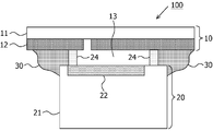
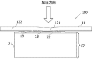
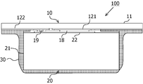
- FIG. 1 is a view showing an example of a pressure sensor according to the embodiment.
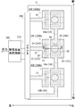
- FIG. 2 is a view showing an example of a pressure sensor according to the embodiment.
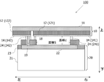
- FIG. 3 is a view showing an example of a pressure sensor according to the embodiment.
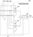
- FIG. 4 is a diagram showing an example of the configuration of a capacitance measurement circuit.
- FIG. 5 is a diagram showing an example of a state before pressure is applied to the pressure sensor.
- FIG. 6 is a diagram showing an example of a state when pressure is applied to the pressure sensor.
- FIG. 7 is a view showing an example of a pressure sensor according to the embodiment.
- FIG. 8 is a view showing an example of a pressure sensor according to the embodiment.
- FIG. 9 is a view showing an example of a pressure sensor according to the embodiment.
- FIG. 1 is a view showing an example of a pressure sensor according to the embodiment.
- FIG. 2 is a view showing an example of a pressure sensor according to the embodiment.
- FIG. 3 is
- FIG. 10A is a first view showing an example of a manufacturing process of the pressure sensor according to the embodiment.
- FIG. 10B is a second view showing an example of a manufacturing process of the pressure sensor according to the embodiment.
- FIG. 10C is a third diagram illustrating an example of a manufacturing process of the pressure sensor according to the embodiment.
- FIG. 10D is a fourth drawing showing an example of the manufacturing process of the pressure sensor according to the embodiment.
- FIG. 10E is a fifth diagram illustrating an example of a manufacturing process of the pressure sensor according to the embodiment.
- FIG. 10F is a sixth drawing showing an example of the manufacturing process of the pressure sensor according to the embodiment.
- FIG. 10G is a seventh drawing showing an example of the manufacturing process of the pressure sensor according to the embodiment.
- FIG. 10H is an eighth diagram showing an example of a manufacturing process of the pressure sensor according to the embodiment.
- FIG. 10I is a ninth view showing an example of a manufacturing process of the pressure sensor according to the embodiment.
- FIG. 10J is a tenth diagram illustrating the example of the manufacturing process of the pressure sensor according to the embodiment.
- FIG. 1 is a view showing an example of a pressure sensor according to the embodiment.
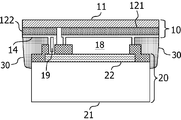
- FIG. 1 is an example of a cross-sectional view of a pressure sensor 100.
- the pressure sensor 100 is an example of a capacitive pressure sensor.
- the pressure sensor 100 includes the sheet substrate 11 and the movable electrode 12, includes the flexible movable portion 10, the substrate portion 21, the fixed electrode 22 and the fixed substrate side plated portion 24, and is hollow between the movable portion 10.
- a fixed substrate portion 20 disposed opposite to the movable portion 10 via the portion 13.
- the fixed electrode 22 is disposed to face the movable electrode 12.
- the movable portion 10 is an example of a flexible substrate.
- the movable electrode 12 is an example of a first electrode.
- the fixed substrate unit 20 is an example of a hard substrate.
- the fixed electrode 22 is an example of a second electrode.
- the pressure sensor 100 includes a fixed substrate side plated portion 24 provided so as to surround the hollow portion 13 between the movable portion 10 and the fixed substrate portion 20.
- the pressure sensor 100 is provided with a reinforcing resin 30 provided around the fixed substrate side plated portion 24 and between the movable portion 10 and the fixed substrate portion 20.
- the reinforcing resin 30 is a member that bonds the movable portion 10 and the fixed substrate portion 20 but does not inhibit the deformation of the movable portion 10, and has a smaller rigidity than the movable portion 10 and the fixed substrate portion 20.
- the fixed substrate side plated portion 24 joins the movable portion 10 and the fixed substrate portion 20.
- the fixed substrate plating portion 24 is an example of a bonding portion.
- the pressure sensor 100 is directed toward the surface of the movable electrode 12 facing the fixed electrode 22 by detecting a change in electrostatic capacitance caused by the movable electrode 12 bending relative to the fixed electrode 22 in the hollow portion 13. Measure the applied pressure.
- the reinforcing resin 30 covers a portion of the movable portion 10, a portion of the fixed substrate portion 20, and a portion of the fixed substrate side plated portion 24.
- the reinforcing resin 30 includes a portion of the lower surface of the movable portion 10, a portion of the upper surface of the fixed substrate portion 20, a portion of the side surface of the fixed substrate portion 20, and the fixed substrate side plated portion 24. Covering a part.
- the reinforcing resin 30 covers a part of the movable portion 10 to reinforce the movable portion 10.
- the reinforcing resin 30 covers a part of the fixed substrate portion 20, whereby the fixed substrate portion 20 is reinforced.
- the reinforcing resin 30 covers a part of the fixed substrate side plated portion 24 to reinforce the fixed substrate side plated portion 24.
- the lower surface of the movable portion 10 and the upper surface of the fixed substrate portion 20 face each other. Further, the lower surface of the movable electrode 12 and the upper surface of the fixed substrate portion 20 face each other. Therefore, the lower surface of the movable portion 10 is a surface facing the fixed substrate portion 20 in the movable portion 10, and the upper surface of the fixed substrate portion 20 is a surface facing the movable portion 10 in the fixed substrate portion 20.
- the side surface of the fixed substrate portion 20 is continuous with the upper surface and the lower surface of the fixed substrate portion 20, and is orthogonal to the upper surface and the lower surface of the fixed substrate portion 20.
- a reinforcing resin 30 is provided around the fixed substrate side plating portion 24 between the movable portion 10 and the fixed substrate portion 20, and a portion of the movable portion 10, a portion of the fixed substrate portion 20 and the fixed substrate side By covering a part of the plated portion 24, peeling between the movable portion 10 and the fixed substrate portion 20 is suppressed.
- the reinforcing resin 30 is preferably soft so as not to inhibit the deformation of the movable portion 10.
- FIG. 2 and 3 are diagrams showing an example of a pressure sensor according to the embodiment.
- FIG. 2 is an example of a plan view of the pressure sensor 100
- FIG. 3 is an example of a cross-sectional view taken along the line AA of FIG.
- the fixed-substrate-side plated portion 24, the first hollow portion 18, the second hollow portion 19, the fixed electrode 22, and the substrate portion 21 which are not visible in plan view are shown by dotted lines.
- three pressure sensors 100 (100a, 100b, 100c) are illustrated, as well as a connector 200 and a capacitance measuring circuit 300.
- the three pressure sensors 100 a, 100 b and 100 c share the sheet substrate 11.
- FIG. 2 is an example of a plan view of the pressure sensor 100
- FIG. 3 is an example of a cross-sectional view taken along the line AA of FIG.
- the fixed-substrate-side plated portion 24, the first hollow portion 18, the second hollow portion 19, the fixed electrode 22, and the substrate portion 21 which are not visible in plan view
- the pressure sensor 100 includes the movable portion 10 having the movable electrode 12 and the fixed substrate portion 20 including the flexible electrode 22.
- the pressure sensor 100 is formed by bonding the movable portion 10 and the fixed substrate portion 20 so that the movable electrode 12 of the movable portion 10 and the fixed electrode 22 of the fixed substrate portion 20 face each other.
- the movable electrode 12 includes a first movable electrode 121 and a second movable electrode 122 provided separately from the first movable electrode 121.
- a first hollow portion 18 is formed between the first movable electrode 121 and the fixed electrode 22. By forming the first hollow portion 18, the movable portion 10 can be deformed toward the fixed substrate portion 20 when pressure is applied to a region on the sheet substrate 11 corresponding to the first movable electrode 121.
- a second hollow portion 19 is formed between the second movable electrode 122 and the fixed electrode 22.
- the cross-sectional shapes of the first hollow portion 18 and the second hollow portion 19 are substantially circular, but the cross-sectional shapes of the first hollow portion 18 and the second hollow portion 19 are limited to substantially circular. is not.
- the cross-sectional shapes of the first hollow portion 18 and the second hollow portion 19 may be formed into a substantially polygonal shape, and may be, for example, a substantially square, a substantially hexagonal, a substantially octagonal, or the like.
- the direction from the second hollow portion 19 to the first hollow portion 18 in FIG. 2 is referred to as the right, and the opposite direction is referred to as the left.
- the direction from the pressure sensor 100 a to the pressure sensor 100 c is rear, and the opposite direction is front.
- the direction from the movable portion 10 to the fixed substrate portion 20 in FIG. 3 is downward, and the opposite direction is upward.
- the movable portion 10 includes a sheet substrate 11, a movable electrode 12, and a movable portion side plated portion 14.
- the sheet substrate 11 is formed of a flexible member (for example, polyimide).
- the thickness of the sheet substrate 11 is, for example, 25 ⁇ m.
- the thickness of the sheet substrate 11 is the length of the sheet substrate 11 in the vertical direction.
- the lower surface of the sheet substrate 11 is provided with a movable electrode 12 formed of a conductive member (for example, copper).
- the movable electrode 12 includes the first movable electrode 121 and the second movable electrode 122 provided to be separated from the first movable electrode 121 as described above.
- the thickness of the movable electrode 12 is, for example, 10 ⁇ m.
- the length of the first movable electrode 121 in the left-right direction is, for example, 2.0 mm.
- the length of the second movable electrode 122 in the left-right direction is, for example, 0.5 mm.
- the lengths of the first movable electrode 121 and the second movable electrode 122 in the front-rear direction are, for example, 1 mm to 2 mm.
- the distance between the first movable electrode 121 and the second movable electrode 122 is, for example, 0.1 mm.
- the movable portion side plated portion 14 is provided on the lower surface of the movable electrode 12.
- the movable portion-side plated portion 14 includes a first plated portion 141 provided on the lower surface of the first movable electrode 121 and a second plated portion 142 provided on the lower surface of the second movable electrode 122.
- the movable portion-side plated portion 14 is formed, for example, by gold plating.
- the fixed substrate portion 20 includes a substrate portion 21, a fixed electrode 22, an insulating portion 23 and a fixed substrate side plated portion 24.
- the substrate unit 21 is formed of a member (for example, glass) which is not easily deformed.
- the thickness of the substrate portion 21 is, for example, 300 ⁇ m to 600 ⁇ m. Since the substrate portion 21 is formed of a member that is not easily deformed, deformation of the fixed substrate portion 20 is suppressed even if the movable portion 10 is bent by the application of pressure to the sheet substrate 11.
- a fixed electrode 22 formed of a conductive member (for example, chromium) is disposed on the upper surface of the substrate unit 21.
- an insulating portion 23 is provided which surrounds the periphery of the fixed electrode 22 and covers a part of the upper side of the fixed electrode 22.
- the insulating portion 23 is formed of an insulator (for example, tetraethoxysilane (TEOS) or silicon dioxide).
- TEOS tetraethoxysilane
- the thickness of the insulating portion 23 is, for example, 0.5 ⁇ m.
- a portion for forming a part of the first hollow portion 18 described above is provided in a part of a region where the first movable electrode 121 and the fixed electrode 22 overlap in a plan view.
- a part for forming the above-described second hollow portion 19 is provided in a part of a region where the second movable electrode 122 and the fixed electrode 22 overlap in plan view.
- a portion for forming a part of the first hollow portion 18 and the second hollow portion 19 is formed as a through hole extending from the surface on the movable portion 10 side of the insulating portion 23 to the surface on the fixed electrode 22 side. Be done.
- the diameter of the first hollow portion 18 in plan view is, for example, 0.6 mm to 1.2 mm. When the pressure sensor 100 is viewed in plan, the area of the second hollow portion 19 is smaller than the area of the first hollow portion 18.
- the diameter of the second hollow portion 19 in plan view is smaller than the diameter of the first hollow portion 18 in plan view.
- the distance d between the first movable electrode 121 of the first hollow portion 18 and the fixed electrode 22 when no pressure is applied is, for example, 1 ⁇ m.
- a fixed substrate plating portion 24 is provided on the inner side surface and the bottom of the second hollow portion 19 in addition to a part of the upper surface of the insulating portion 23.
- the fixed substrate plating portion 24 includes a third plating portion 241 and a fourth plating portion 242.
- the third plated portion 241 is provided in a region near the edge of the through hole that forms a part of the first hollow portion 18 on the upper surface of the insulating portion 23 so as to surround the region.
- a space formed by the portion surrounded by the third plated portion 241 and the through hole provided in the insulating portion 23 in this manner is a first hollow portion.
- the fourth plated portion 242 is provided in a region near the edge of the through hole for forming the second hollow portion 19 on the upper surface of the insulating portion 23 so as to surround the region, and the inner side surface of the through hole And the upper surface of the fixed electrode 22 corresponding to the bottom of the through hole. That is, the fourth plated portion 242 is formed of a portion which is formed to project from the upper surface of the insulating portion 23 toward the second movable electrode 122 and a portion which covers the inside of the through hole, and is surrounded by these The space is the second hollow portion 19.
- the fixed substrate plating portion 24 is formed, for example, by gold plating. By bonding the movable portion-side plated portion 14 and the fixed substrate-side plated portion 24, the movable portion 10 and the fixed substrate portion 20 are integrated to form the pressure sensor 100. In addition, the second movable portion 122 and the fixed electrode 22 are electrically connected by joining the second plated portion 142 and the fourth plated portion 242.
- the second movable electrode 122 and the connector 200 are connected by a signal line 15 extending from the second movable electrode 122.
- the ground (GND) line 16a extending from the first movable electrode 121 is connected between the first movable electrodes 121 of the pressure sensors 100a and 100b and between the first movable electrodes 121 of the pressure sensors 100b and 100c.
- the distance between adjacent pressure sensors 100 is, for example, 0.1 mm to 0.3 mm. That is, the length of the GND line 16a is 0.1 mm to 0.3 mm.
- the first movable electrode 121 of the pressure sensor 100 c is connected to the connector 200 by the GND line 16 b extending from the first movable electrode 121.
- GND is shared by the pressure sensors 100a, 100b, and 100c.
- both the signal line 15 and the GND line 16 are formed on the lower surface of the sheet substrate 11. That is, in the pressure sensor 100, the wiring extending from the first movable electrode 121 and the wiring extending from the fixed electrode 22 are formed in the same layer.
- the pressure sensor 100 can realize a simple wiring structure by adopting such a configuration.
- the pressure sensor 100 having the above-described configuration includes an area overlapping the fixed electrode 22 of the first movable electrode 121 and an area overlapping the first movable electrode 121 of the fixed electrode 22 which are arranged at a distance d (see FIG. 3). It works as a plate capacitor.
- the capacitance C of the capacitor is calculated, for example, by the following equation 1 using the distance d described above and the area S of the area where the first movable electrode 121 and the fixed electrode 22 overlap (see FIG. 3). .
- ⁇ 0 is the dielectric constant of vacuum
- ⁇ r is the dielectric constant of the atmosphere. That is, according to (Expression 1), the electrostatic capacitance C fluctuates according to the fluctuation of the distance d between the first movable electrode 121 and the fixed electrode 22 which is caused by the force applied to the movable portion 10. I understand.
- the pressure P is calculated by the following (Formula 2), for example using the area S mentioned above.
- F is the magnitude of the force applied to the pressure sensor 100.
- the substrate unit 21 is formed of a member that is not easily deformed, even if a force is applied to the pressure sensor 100, the fluctuation of the area S serving as a reference of pressure calculation is suppressed. Therefore, the pressure sensor 100 can detect the pressure with higher accuracy than a pressure sensor formed of a member that the substrate portion 21 is easily deformed.
- FIG. 4 is a diagram showing an example of the configuration of the capacitance measuring circuit 300. As shown in FIG. In FIG. 4, pressure sensors 100 a, 100 b and 100 c are also illustrated. Further, in FIG. 4, the illustration of the connector 200 is omitted.
- the capacitance measurement circuit 300 includes two multiplexers 301 and 301 (denoted as MUX in the drawing) and a converter 302. Signals associated with fluctuations in capacitance of the pressure sensors 100 a, 100 b, 100 c are input to the multiplexers 301, 301 via the signal line 15. Each of the multiplexers 301 and 301 outputs a selected one of the signals input from the pressure sensors 100a, 100b and 100c.
- MUX multiplexers
- the signal output from each of the multiplexers 301 and 301 is input to the converter 302.
- the converter 302 stores, for example, the correspondence between signal values input from the multiplexers 301 and 301 and pressure.
- the correspondence relationship managed by the converter 302 may be, for example, a table indicating the correspondence between the input signal value and the pressure, or may be a mathematical expression for calculating the pressure from the input signal value.
- the converter 302 converts, for example, the signal value input from the multiplexers 301 and 301 into a signal value indicating pressure according to the correspondence relationship, and outputs a signal value indicating pressure.
- FIG. 5 shows an example of a state before pressure is applied to the pressure sensor 100
- FIG. 6 shows an example of a state when pressure is applied to the pressure sensor 100.
- the pressure sensor 100 when pressure is applied from above the first hollow portion 18, as illustrated in FIG. 6, the pressure is applied according to the force applied to the movable portion 10 including the sheet substrate 11 and the first movable electrode 121. And bend toward the fixed substrate portion 20.
- the pressure sensor 100 returns from the state of FIG. 6 to the state of FIG. That is, in the pressure sensor 100, the distance d between the first movable electrode 121 and the fixed electrode 22 fluctuates according to the applied force.
- the capacitance of the pressure sensor 100 changes according to (Expression 1).
- the pressure applied to the pressure sensor 100 is detected by measuring the fluctuation of the capacitance of the pressure sensor 100 by the capacitance measuring circuit 300 illustrated in FIG. 2.
- the pressure sensor 100 has a second hollow portion 19 in addition to the first hollow portion 18.
- the cylindrical fourth plating portion 242 which reaches from the fixed electrode 22 to the second movable electrode 122 is formed. If the fixed electrode 22 and the second movable electrode 122 are only electrically connected, it is sufficient to connect only one wire instead of forming the fourth plated portion 242 in a cylindrical shape.
- both of the first movable electrode 121 and the second movable electrode 122 provided apart from each other are provided on the sheet substrate 11.
- the first movable electrode 121 when a force is applied from above the first movable electrode 121, the first movable electrode 121 is bent to the fixed electrode 22 side, and the second movable electrode 122 is also distorted to the fixed electrode 22 side.
- the first movable electrode 121 bends with respect to the fixed electrode 22 without deviation in the front-rear direction and the left-right direction.
- the second movable electrode 122 is distorted to the fixed electrode 22 side, the first movable electrode 121 is affected by the deflection, and it becomes difficult to deflect the fixed electrode 22 uniformly.
- the cross-sectional shape when planarly viewing the 4th plated part 242 is formed in substantially circle shape or substantially polygon shape.
- distortion in the second movable electrode 122 portion when pressure is applied is suppressed as compared with the configuration in which the fixed electrode 22 and the second movable electrode 122 are connected by one wire.
- the fourth plated portion 242 having a substantially circular or polygonal cross-sectional shape can support the second movable electrode 122 more stably than in the case where the second movable electrode 122 is supported by one wire. .
- FIGS. 7 and 8 are diagrams showing an example of the pressure sensor according to the embodiment. 7 and 8 are examples of cross-sectional views taken along the line AA of FIG.
- the pressure sensor 100 includes a reinforcing resin 30 provided between the movable portion 10 and the fixed substrate portion 20 around the first hollow portion 18 and the second hollow portion 19.
- the reinforcing resin 30 is provided around the first hollow portion 18 and the second hollow portion 19 and between the movable portion 10 and the fixed substrate portion 20.
- the reinforcing resin 30 bonds the movable portion 10 and the fixed substrate portion 20.
- FIG. 1 is bonded to bond the movable portion 10 and the fixed substrate portion 20.
- the reinforcing resin 30 covers a portion of the lower surface of the movable portion 10, a portion of the upper surface of the fixed substrate portion 20, and a portion of the side surface of the fixed substrate portion 20.
- the reinforcing resin 30 covers a portion of the lower surface of the movable portion 10, a portion of the upper surface of the fixed substrate portion 20, and the side and lower surfaces of the fixed substrate portion 20.
- the reinforcing resin 30 covers a portion of the movable portion 10 and a portion of the fixed substrate portion 20, whereby the movable portion 10 and the fixed substrate portion 20 are reinforced.
- a single reinforcing resin 30 may cover a portion of the movable portion 10 and a portion of the fixed substrate portion 20, and a plurality of reinforcing resins 30 may be a portion of the movable portion 10 and a portion of the fixed substrate portion 20. You may cover it.
- the pressure sensors of FIGS. 7 and 8 are exemplary and are not limited to the examples of pressure sensors of FIGS. 7 and 8.
- the reinforcing resin 30 may cover a portion of the lower surface of the movable portion 10 and a portion of the upper surface of the fixed substrate portion 20, and may cover all of the side surfaces of the fixed substrate portion 20 and a portion of the lower surface.
- the reinforcing resin 30 may cover a portion of the lower surface of the movable portion 10 and a portion of the upper surface of the fixed substrate portion 20 and a portion of the side surface and the lower surface of the fixed substrate portion 20.
- the reinforcing resin 30 may cover a portion of the lower surface of the movable portion 10 and a portion of the upper surface of the fixed substrate portion 20, and may cover a portion of the side surface and the entire lower surface of the fixed substrate portion 20.
- FIG. 9 is a view showing an example of a pressure sensor according to the embodiment.
- FIG. 9 is an example of a cross-sectional view taken along the line AA of FIG.
- the reinforcing resin 30 is in contact with the sheet substrate 11, the movable electrode 12 and the movable portion side plated portion 14.
- the reinforcing resin 30 may be in contact with the movable electrode 12 and the movable portion-side plated portion 14 and not in contact with the sheet substrate 11 without being limited to the example shown in FIG. Further, the reinforcing resin 30 may be in contact with the movable portion side plated portion 14 and not in contact with the sheet substrate 11 and the movable electrode 12. As shown in FIG.
- a third plated portion 241 provided so as to surround the first hollow portion 18 and a second hollow portion 19 are provided between the movable portion 10 and the fixed substrate portion 20.
- the fourth plated portion 242 is disposed. Therefore, the reinforcing resin 30 is provided around the fixed substrate side plated portion 24 including the third plated portion 241 and the fourth plated portion 242.
- the reinforcing resin 30 covers a portion of the third plated portion 241 and a portion of the fourth plated portion 242.
- the reinforcing resin 30 covers a part of the third plated part 241 and a part of the fourth plated part 242, thereby reinforcing the third plated part 241 and the fourth plated part 242.
- a single reinforcing resin 30 may cover a portion of the movable portion 10 and a portion of the fixed substrate portion 20, a portion of the third plated portion 241, and a portion of the fourth plated portion 242.
- the plurality of reinforcing resins 30 may cover a portion of the movable portion 10, a portion of the fixed substrate portion 20, a portion of the third plated portion 241, and a portion of the fourth plated portion 242.
- a single reinforcing resin 30 may cover a portion of the movable portion 10, a portion of the fixed substrate portion 20, a portion of the third plated portion 241, and a portion of the fourth plated portion 242.
- the plurality of reinforcing resins 30 may cover a portion of the movable portion 10, a portion of the fixed substrate portion 20, a portion of the third plated portion 241, and a portion of the fourth plated portion 242.
- a reinforcing resin 30 is embedded between the movable portion 10 and the fixed substrate portion 20 around the first hollow portion 18 and the second hollow portion 19, and a part of the movable portion 10, one of the fixed substrate portion 20.
- peeling between the movable portion 10 and the fixed substrate portion 20 is suppressed.
- the peeling between the movable portion 10 and the fixed substrate portion 20 is further suppressed. Bonding of the movable portion 10 and the fixed substrate portion 20 by the reinforcing resin 30 maintains the bonding between the movable portion 10 and the fixed substrate portion 20, and the peeling between the movable portion 10 and the fixed substrate portion 20 is suppressed. .
- the movable portion 10 and the fixed substrate portion 20 are joined by joining the movable portion-side plated portion 14 and the fixed substrate side plated portion 24.
- the reinforcing resin 30 covers a portion of the movable portion 10, a portion of the fixed substrate portion 20, and a portion of the fixed substrate side plated portion 24 so that the bonding between the movable portion 10 and the fixed substrate portion 20 is maintained. Peeling between the portion 10 and the fixed substrate side plated portion 24 is suppressed.
- the reinforcement resin 30 is embedded between the movable portion 10 and the fixed substrate portion 20 around the first hollow portion 18 and the second hollow portion 19 so that the intrusion of water into the pressure sensor 100 is suppressed. The short circuit of the pressure sensor 100 is suppressed.
- the reinforcing resin 30 may cover either one or both of the signal line 15 and the GND line 16 shown in FIG.
- the reinforcing resin 30 covering the signal line 15 and the GND line 16 suppresses the disconnection of the signal line 15 and the GND line 16.
- the reinforcing resin 30 be soft so as not to inhibit the deformation of the movable portion 10 when a pressure is applied to the pressure sensor 100.
- the reinforcing resin 30 include epoxy resin and polyimide resin.
- the Young's modulus (elastic modulus) of the reinforcing resin 30 be the same as the Young's modulus of the movable portion 10 or smaller than the Young's modulus of the movable portion 10.
- the Young's modulus of the movable portion 10 is smaller than the Young's modulus of the fixed substrate portion 20.
- the Young's modulus (E1) of the reinforcing resin 30, the Young's modulus (E2) of the movable portion 10, and the Young's modulus (E3) of the fixed substrate portion 20 may be in the order of E1 ⁇ E2 ⁇ E3.
- the material of the sheet substrate 11 and the material of the reinforcing resin 30 may be the same.
- the Young's modulus of the movable electrode 12 is larger than the Young's modulus of the sheet substrate 11 and the reinforcing resin 30.
- the Young's modulus of the reinforcing resin 30 is smaller than the Young's modulus of the movable portion 10.
- the bending stress ⁇ can be determined by the bending moment M / the cross section coefficient Z.
- the width of each of the movable portion 10, the fixed substrate portion 20, and the reinforcing resin 30 is constant, as the thickness T of each of the movable portion 10, the fixed substrate portion 20, and the reinforcing resin 30 decreases, the movable portion 10, the fixed substrate
- the section coefficient Z of each of the portion 20 and the reinforcing resin 30 becomes smaller.
- the section coefficient Z of each of the movable portion 10 becomes smaller, the bending stress ⁇ of each of the movable portion 10, the fixed substrate portion 20 and the reinforcing resin 30 becomes larger. Therefore, when the respective widths of the movable portion 10, the fixed substrate portion 20, and the reinforcing resin 30 are constant, as the thickness T of the movable portion 10, the fixed substrate portion 20, and the reinforcing resin 30 decreases, the movable portion 10, The rigidity of each of the fixed substrate portion 20 and the reinforcing resin 30 is reduced.
- the thickness (T1) of the reinforcing resin 30, the thickness (T2) of the movable portion 10, and the thickness (T3) of the fixed substrate portion 20 are The order may be T1 ⁇ T2 ⁇ T3.
- the pressure sensor 100 has a plurality of sensor elements that share a single sheet substrate 11.
- a plurality of reinforcing resins 30 are disposed on a single sheet substrate 11, and each of the plurality of reinforcing resins 30 covers each movable electrode 12, each fixed substrate portion 20, and each fixed substrate side plated portion 24.
- the plurality of movable electrodes 12 are separated, the plurality of fixed substrate portions 20 are separated, the plurality of fixed substrate side plated portions 24 are separated, and the plurality of reinforcing resins 30 are separated. Therefore, when pressure is applied to the pressure sensor 100, one of the adjacent sensor elements does not inhibit the deformation of the movable portion 10 included in the other of the adjacent sensor elements. Therefore, the deformation of the movable portion 10 when the pressure is applied to the pressure sensor 100 is not inhibited, and the pressure applied to the pressure sensor 100 can be measured with high accuracy.
- 10A to 10I are diagrams showing an example of a manufacturing process of the pressure sensor 100.
- FIG. Hereinafter, an example of a manufacturing process of the pressure sensor 100 will be described with reference to FIGS. 10A to 10I.
- FIG. 10A to 10E show an example of the manufacturing process of the fixed substrate portion 20.
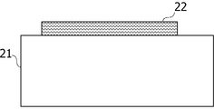
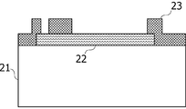
- FIG. 10A the fixed electrode 22 is formed on the surface of the substrate 21 facing the movable portion 10.
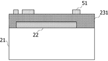
- FIG. 10B the insulating film 231 is formed so as to cover the fixed electrode 22.
- a resist film 51 is formed on the surface of the insulating film 231 facing the movable portion 10.
- FIG. 10C a resist film 51 having a predetermined pattern is formed on the insulating film 231 by performing a photoresist using a photomask in which a desired pattern is formed on the resist film 51.
- FIG. 10C a resist film 51 having a predetermined pattern is formed on the insulating film 231 by performing a photoresist using a photomask in which a desired pattern is formed on the resist film 51.
- the etching process is performed, and the resist film 51 is further removed, whereby the insulating portion 23 is formed.
- the fixed substrate side plated portion 24 is formed on the surface of the insulating portion 23 facing the movable portion 10.
- the plating resist is performed on the area where the fixed substrate side plated portion 24 is not formed, and then the plating process is performed to form the fixed substrate side plated portion 24 in a desired area.
- the fixed substrate side plated portion 24 may be formed by sputtering. That is, after a plating layer is formed on the surface of the insulating portion 23 facing the movable portion 10 by a sputtering apparatus, a resist is applied and etched to form a pattern of the fixed substrate plating portion 24. May be
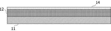
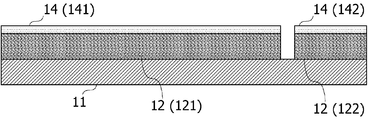
- FIG. 10F the movable electrode 12 is formed on the surface of the flexible sheet substrate 11 facing the fixed substrate portion 20. Furthermore, the plating process is performed on the surface of the movable electrode 12 facing the fixed substrate portion 20, whereby the movable portion-side plated portion 14 is formed.
- the etching resist is performed on the region corresponding to the first movable electrode 121 and the second movable electrode 122 on the surface of the movable portion plating portion 14 facing the fixed substrate portion 20, and then the etching is performed. By being performed, the first movable electrode 121 and the second movable electrode 122 are formed.
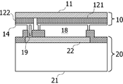
- FIG. 10H and FIG. 10I show an example of the process of joining the fixed substrate part 20 and the movable part 10.
- the movable portion 10 and the fixed substrate portion 20 are joined.
- the movable portion 10 and the fixed substrate portion 20 may be joined by, for example, normal temperature bonding.
- the normal temperature bonding for example, the surface of the movable portion side plated portion 14 of the movable portion 10 facing the fixed substrate portion 20 and the surface of the fixed substrate portion 20 facing the movable portion 10 of the fixed substrate side plated portion 24 are A process of smoothing the surface and a process of removing impurities from the surface to clean the surface are performed.
- FIG. 10I illustrates a state in which three pressure sensors 100 manufactured by the steps of FIGS. 10A to 10H are arranged side by side so as to share the sheet substrate 11. As illustrated in FIG. 10I, the pressure sensor 100 can widen the area targeted for pressure detection by sharing the sheet substrate 11 and arranging the plurality of pressure sensors 100.
- manufacturing of the movable portion 10 and the fixed substrate portion 20 is performed without performing a process of flattening the surfaces of the movable portion side plated portion 14 and the fixed substrate side plated portion 24.
- the flatness of the surface may be ensured in the process.
- metal for example, copper
- CMP Chemical Mechanical Polishing
- FIG. 10J shows an example of the process of forming the reinforcing resin 30.
- the reinforcing resin 30 is formed around the first hollow portion 18 and the second hollow portion 19 and between the movable portion 10 and the fixed substrate portion 20.
- the reinforcing resin 30 is formed on a portion of the lower surface of the movable portion 10 and the side surface of the fixed substrate portion 20.
- the reinforcing resin 30 may be applied to the movable portion 10 and the fixed substrate portion 20 by a dispenser.
- the sheet-like reinforcing resin 30 may be attached to the movable portion 10 and the fixed substrate portion 20.
- Second hollow portion 20 Fixed substrate portion 21: Substrate portion 22: Fixed electrode 23: Insulation portion 24: Fixed substrate side plated portion 241: Third plating Section 242 Fourth plating section 30 Reinforcing resin 51 Resist film 200 Connector 231 Insulating film 300 Capacitance measurement circuit 301 Multiplexer 302 converter
Landscapes
- Physics & Mathematics (AREA)
- General Physics & Mathematics (AREA)
- Measuring Fluid Pressure (AREA)
- Pressure Sensors (AREA)
Abstract
フレキシブル基板と硬質基板との剥離を抑制する。静電容量式圧力センサは、第1の電極を含み、可撓性を有するフレキシブル基板と、第1の電極に対向して配置される第2の電極を含み、フレキシブル基板との間に中空部を介してフレキシブル基板に対向配置された硬質基板と、フレキシブル基板と硬質基板との間であって、中空部を囲むように設けられ、フレキシブル基板と硬質基板とを接合する接合部と、接合部の周囲であって、フレキシブル基板と硬質基板との間に設けられた補強樹脂と、を備え、中空部において、第1の電極が第2の電極に対して撓むことで生じる静電容量の変化を検出することにより、第1の電極における第2の電極との対向面に向けて印加される圧力を測定し、補強樹脂が、フレキシブル基板の一部、硬質基板の一部および接合部の一部を覆っている。
Description
本発明は、静電容量式圧力センサに関する。
圧力センサは、主として気体や液体の圧力を検出するものであり、気圧センサや高度センサ、水圧センサとして各種の装置に適用されている。また、近年においては、これを高度センサとして利用する場合の一態様として、位置情報を得るためのナビゲーション装置への応用やユーザの運動量を精緻に計測する計測器への応用等、その適用範囲が広がりつつある。
MEMS(Micro Electro Mechanical System)センサチップとしての静電容量式圧力センサが知られている。静電容量式圧力センサは、可動電極を有するフレキシブル基板と、固定電極を有する硬質基板とを備えている。可動電極と固定電極との間には、ギャップに応じた静電容量が発生する。静電容量式圧力センサに圧力が印加されることにより、フレキシブル基板が撓み、可動電極と固定電極との間のギャップが変化することで、静電容量の変化を検出する。静電容量の変化に応じた圧力が検出される。静電容量式半導体物理量センサが提案されている(特許文献1参照)。
静電容量式圧力センサに圧力が繰り返して印加されることで、フレキシブル基板と硬質基板とが剥離する可能性がある。このような状況に鑑み、本発明は、フレキシブル基板と硬質基板との剥離を抑制した静電容量式圧力センサを提供することを目的とする。
本発明では、上記課題を解決するために、以下の手段を採用した。すなわち、本発明は、第1の電極を含み、可撓性を有するフレキシブル基板と、第1の電極に対向して配置される第2の電極を含み、フレキシブル基板との間に中空部を介してフレキシブル基板に対向配置された硬質基板と、フレキシブル基板と硬質基板との間であって、中空部を囲むように設けられ、フレキシブル基板と硬質基板とを接合する接合部と、接合部の周囲であって、フレキシブル基板と硬質基板との間に設けられた補強樹脂と、を備え、中空部において、第1の電極が第2の電極に対して撓むことで生じる静電容量の変化を検出することにより、第1の電極における第2の電極との対向面に向けて印加される圧力を測定する、静電容量式圧力センサであって、補強樹脂が、フレキシブル基板の一部、硬質基板の一部および接合部の一部を覆っている。
補強樹脂が、フレキシブル基板の一部を覆うことで、フレキシブル基板が補強される。補強樹脂が、硬質基板の一部を覆うことで、硬質基板が補強される。補強樹脂が、接合部の一部を覆うことで、接合部が補強される。補強樹脂が、フレキシブル基板、硬質基板および接合部を補強することで、フレキシブル基板と硬質基板との接合が維持され、フレキシブル基板と硬質基板との剥離が抑制される。
上記静電容量式圧力センサにおいて、補強樹脂のヤング率が、フレキシブル基板のヤング率と同一であり又はフレキシブル基板のヤング率よりも小さくてもよく、フレキシブル基板のヤング率が、硬質基板のヤング率よりも小さくてもよい。これにより、静電容量式圧力センサに圧力が印加された際におけるフレキシブル基板の変形が阻害されず、静電容量式圧力センサに印加された圧力を高い精度で測定することができる。
上記静電容量式圧力センサにおいて、補強樹脂の厚みが、フレキシブル基板の厚みと同一であってもよく又はフレキシブル基板の厚みよりも小さくてもよく、フレキシブル基板の厚みが、硬質基板の厚みよりも小さくてもよい。これにより、静電容量式圧力センサに圧力が印加された際におけるフレキシブル基板の変形が阻害されず、静電容量式圧力センサに印加された圧力を高い精度で測定することができる。
上記静電容量式圧力センサにおいて、補強樹脂が、硬質基板におけるフレキシブル基板との対向面の一部と、硬質基板の側面と、硬質基板におけるフレキシブル基板との対向面の反対面の少なくとも一部とを覆っていてもよい。硬質基板におけるフレキシブル基板との対向面は、硬質基板の上面である。硬質基板におけるフレキシブル基板との対向面の反対面は、硬質基板の下面である。硬質基板の側面は、硬質基板の上面および下面と連続しており、硬質基板の上面および下面と直交している。補強樹脂が、硬質基板におけるフレキシブル基板との対向面の一部と、硬質基板の側面と、硬質基板の下面の少なくとも一部を覆うことで、フレキシブル基板と硬質基板との剥離が更に抑制される。
上記静電容量式圧力センサにおいて、フレキシブル基板は第1の電極を複数含んでよく、複数の第1の電極に対応する複数の第2の電極、複数の硬質基板、複数の接合部および複数の補強樹脂を備えてもよい。これにより、フレキシブル基板と複数の硬質基板との接合が維持され、フレキシブル基板と複数の硬質基板との剥離が抑制される。
本発明によれば、フレキシブル基板と硬質基板との剥離を抑制した静電容量式圧力センサを提供することができる。
以下、実施形態について図を参照しながら説明する。以下に示す実施形態は、本願の一態様であり、本願の技術的範囲を限定するものではない。
<適用例>
図1は実施形態に係る圧力センサの一例を示す図である。図1は圧力センサ100の断面図の一例である。圧力センサ100は、静電容量式圧力センサの一例である。圧力センサ100は、シート基板11および可動電極12を含み、可撓性を有する可動部10と、基板部21、固定電極22および固定基板側メッキ部24を含み、可動部10との間に中空部13を介して可動部10に対向配置された固定基板部20とを備える。固定電極22は、可動電極12に対向して配置されている。可動部10は、フレキシブル基板の一例である。可動電極12は、第1の電極の一例である。固定基板部20は、硬質基板の一例である。固定電極22は、第2の電極の一例である。また、圧力センサ100は、可動部10と固定基板部20との間であって、中空部13を囲むように設けられた固定基板側メッキ部24を備える。更に、圧力センサ100は、固定基板側メッキ部24の周囲であって、可動部10と固定基板部20との間に設けられた補強樹脂30を備える。補強樹脂30は、可動部10と固定基板部20とを接着するが、可動部10の変形を阻害しない部材であり、可動部10および固定基板部20よりも剛性が小さい。固定基板側メッキ部24は、可動部10と固定基板部20とを接合する。固定基板側メッキ部24は、接合部の一例である。圧力センサ100は、中空部13において、可動電極12が固定電極22に対して撓むことで生じる静電容量の変化を検出することにより、可動電極12における固定電極22との対向面に向けて印加される圧力を測定する。
図1は実施形態に係る圧力センサの一例を示す図である。図1は圧力センサ100の断面図の一例である。圧力センサ100は、静電容量式圧力センサの一例である。圧力センサ100は、シート基板11および可動電極12を含み、可撓性を有する可動部10と、基板部21、固定電極22および固定基板側メッキ部24を含み、可動部10との間に中空部13を介して可動部10に対向配置された固定基板部20とを備える。固定電極22は、可動電極12に対向して配置されている。可動部10は、フレキシブル基板の一例である。可動電極12は、第1の電極の一例である。固定基板部20は、硬質基板の一例である。固定電極22は、第2の電極の一例である。また、圧力センサ100は、可動部10と固定基板部20との間であって、中空部13を囲むように設けられた固定基板側メッキ部24を備える。更に、圧力センサ100は、固定基板側メッキ部24の周囲であって、可動部10と固定基板部20との間に設けられた補強樹脂30を備える。補強樹脂30は、可動部10と固定基板部20とを接着するが、可動部10の変形を阻害しない部材であり、可動部10および固定基板部20よりも剛性が小さい。固定基板側メッキ部24は、可動部10と固定基板部20とを接合する。固定基板側メッキ部24は、接合部の一例である。圧力センサ100は、中空部13において、可動電極12が固定電極22に対して撓むことで生じる静電容量の変化を検出することにより、可動電極12における固定電極22との対向面に向けて印加される圧力を測定する。
補強樹脂30は、可動部10の一部、固定基板部20の一部および固定基板側メッキ部24の一部を覆っている。図1の例では、補強樹脂30は、可動部10の下面の一部と、固定基板部20の上面の一部と、固定基板部20の側面の一部と、固定基板側メッキ部24の一部とを覆っている。補強樹脂30が、可動部10の一部を覆うことにより、可動部10が補強される。補強樹脂30が、固定基板部20の一部を覆うことにより、固定基板部20が補強される。補強樹脂30が、固定基板側メッキ部24の一部を覆うことにより、固定基板側メッキ部24が補強される。可動部10の下面と固定基板部20の上面とが対向している。また、可動電極12の下面と固定基板部20の上面とが対向している。したがって、可動部10の下面は、可動部10における固定基板部20との対向面であり、固定基板部20の上面は、固定基板部20における可動部10との対向面である。固定基板部20の側面は、固定基板部20の上面および下面と連続しており、固定基板部20の上面および下面と直交している。補強樹脂30が、固定基板側メッキ部24の周囲であって、可動部10と固定基板部20との間に設けられ、可動部10の一部、固定基板部20の一部および固定基板側メッキ部24の一部を覆うことで、可動部10と固定基板部20との剥離が抑制される。補強樹脂30は、可動部10の変形を阻害しないように柔らかいことが好ましい。
<実施例>
図2および図3は実施形態に係る圧力センサの一例を示す図である。図2は圧力センサ100を平面視した図の一例であり、図3は図2のA-A線における断面図の一例である。図2では、平面視においては目視できない固定基板側メッキ部24、第1中空部18、第2中空部19、固定電極22および基板部21が点線で示されている。図2では、3つの圧力センサ100(100a、100b、100c)が例示されるとともに、コネクタ200および静電容量測定回路300も例示される。3つの圧力センサ100a、100b、100cは、シート基板11を共有する。図3を参照すると理解できるように、圧力センサ100は、可動電極12を含み可撓性を有する可動部10と固定電極22を含む固定基板部20とを備える。圧力センサ100は、可動部10の可動電極12と固定基板部20の固定電極22とが対向するように、可動部10と固定基板部20とを接合して形成される。可動電極12は、第1可動電極121および第1可動電極121と離間して設けられる第2可動電極122を含む。第1可動電極121と固定電極22との間には、第1中空部18が形成される。第1中空部18が形成されることで、シート基板11上の第1可動電極121に相当する領域に圧力が印加されたときに、可動部10は固定基板部20に向けて変形可能となる。また、第2可動電極122と固定電極22との間には、第2中空部19が形成される。図2では、第1中空部18および第2中空部19の断面形状は略円形に形成されているが、第1中空部18および第2中空部19の断面形状が略円形に限定されるわけではない。第1中空部18および第2中空部19の断面形状は、略多角形に形成されていてもよく、例えば、略四角形、略六角形、略八角形等であってもよい。以下、本明細書において、図2における第2中空部19から第1中空部18に向かう方向を右、その逆方向を左とする。また、図2において、圧力センサ100aから圧力センサ100cに向かう方向を後ろ、その逆方向を前とする。さらに、図3における可動部10から固定基板部20に向かう方向を下、その逆方向を上とする。
図2および図3は実施形態に係る圧力センサの一例を示す図である。図2は圧力センサ100を平面視した図の一例であり、図3は図2のA-A線における断面図の一例である。図2では、平面視においては目視できない固定基板側メッキ部24、第1中空部18、第2中空部19、固定電極22および基板部21が点線で示されている。図2では、3つの圧力センサ100(100a、100b、100c)が例示されるとともに、コネクタ200および静電容量測定回路300も例示される。3つの圧力センサ100a、100b、100cは、シート基板11を共有する。図3を参照すると理解できるように、圧力センサ100は、可動電極12を含み可撓性を有する可動部10と固定電極22を含む固定基板部20とを備える。圧力センサ100は、可動部10の可動電極12と固定基板部20の固定電極22とが対向するように、可動部10と固定基板部20とを接合して形成される。可動電極12は、第1可動電極121および第1可動電極121と離間して設けられる第2可動電極122を含む。第1可動電極121と固定電極22との間には、第1中空部18が形成される。第1中空部18が形成されることで、シート基板11上の第1可動電極121に相当する領域に圧力が印加されたときに、可動部10は固定基板部20に向けて変形可能となる。また、第2可動電極122と固定電極22との間には、第2中空部19が形成される。図2では、第1中空部18および第2中空部19の断面形状は略円形に形成されているが、第1中空部18および第2中空部19の断面形状が略円形に限定されるわけではない。第1中空部18および第2中空部19の断面形状は、略多角形に形成されていてもよく、例えば、略四角形、略六角形、略八角形等であってもよい。以下、本明細書において、図2における第2中空部19から第1中空部18に向かう方向を右、その逆方向を左とする。また、図2において、圧力センサ100aから圧力センサ100cに向かう方向を後ろ、その逆方向を前とする。さらに、図3における可動部10から固定基板部20に向かう方向を下、その逆方向を上とする。
可動部10は、シート基板11、可動電極12、可動部側メッキ部14を含む。シート基板11は、可撓性を有する部材(例えば、ポリイミド)で形成される。シート基板11の厚さは、例えば、25μmである。ここで、シート基板11の厚さは、シート基板11の上下方向の長さである。シート基板11の下方向の面には導電性を有する部材(例えば銅)によって形成される可動電極12が設けられる。可動電極12は、上述のように、第1可動電極121および第1可動電極121と離間して設けられる第2可動電極122を含む。可動電極12の厚さは、例えば、10μmである。第1可動電極121の左右方向の長さは、例えば、2.0mmである。第2可動電極122の左右方向の長さは、例えば、0.5mmである。第1可動電極121および第2可動電極122の前後方向の長さは、例えば、1mmから2mmである。第1可動電極121と第2可動電極122との間の距離は、例えば、0.1mmである。可動電極12の下方向の面には、可動部側メッキ部14が設けられる。可動部側メッキ部14は、第1可動電極121の下方向の面に設けられる第1メッキ部141と第2可動電極122の下方向の面に設けられる第2メッキ部142を含む。可動部側メッキ部14は、例えば、金メッキによって形成される。
固定基板部20は、基板部21、固定電極22、絶縁部23および固定基板側メッキ部24を含む。基板部21は、容易には変形しない部材(例えば、ガラス)で形成される。基板部21の厚さは、例えば、300μmから600μmである。基板部21は容易には変形しない部材で形成されるため、シート基板11への圧力の印加により可動部10が撓んでも、固定基板部20の変形は抑制される。基板部21の上側の面上には導電性を有する部材(例えばクロム)によって形成された固定電極22が配置される。さらに、固定電極22の周囲を囲むとともに、固定電極22の上方の一部を覆う絶縁部23が設けられる。絶縁部23は絶縁体(例えば、テトラエトキシシラン(TEOS)や二酸化ケイ素)によって形成される。絶縁部23の厚さは、例えば、0.5μmである。絶縁部23には、平面視において第1可動電極121と固定電極22とが重なる領域の一部には上述した第1中空部18の一部を形成する箇所が設けられる。また、平面視において第2可動電極122と固定電極22とが重なる領域の一部には上述した第2中空部19を形成するための箇所が設けられる。絶縁部23において、第1中空部18の一部および第2中空部19を形成するための箇所は、絶縁部23の可動部10側の面から固定電極22側の面まで達する貫通孔として形成される。第1中空部18を平面視したときの直径は、例えば、0.6mmから1.2mmである。圧力センサ100を平面視した場合において、第2中空部19の面積は、第1中空部18の面積よりも小さい。すなわち、第2中空部19を平面視したときの直径は、第1中空部18を平面視したときの直径よりも小さい。圧力が印加されていないときにおける第1中空部18の第1可動電極121と固定電極22との間の距離dは、例えば、1μmである。絶縁部23の上側の面の一部の他、第2中空部19の内側面および底部には、固定基板側メッキ部24が設けられる。固定基板側メッキ部24は、第3メッキ部241と第4メッキ部242を含む。第3メッキ部241は、絶縁部23の上側の面において、第1中空部18の一部を形成する貫通孔の縁近傍の領域に当該領域を囲むようにして設けられる。このようにして第3メッキ部241に囲まれた部分と絶縁部23に設けられた貫通孔によって形成される空間が第1中空部である。第4メッキ部242は、絶縁部23の上側の面において、第2中空部19を形成するための貫通孔の縁近傍の領域に、当該領域を囲むようにして設けられるとともに、該貫通孔の内側面、及び該貫通孔の底部に該当する固定電極22の上面にも設けられる。即ち、第4メッキ部242は、絶縁部23の上側の面から第2可動電極122に向けて突出して形成される部分と、貫通孔の内部を覆う部分とから形成され、これらに囲まれた空間が第2中空部19となる。なお、固定基板側メッキ部24は、例えば、金メッキによって形成される。可動部側メッキ部14と固定基板側メッキ部24とが接合されることで可動部10と固定基板部20とが一体となり、圧力センサ100が形成される。また、第2メッキ部142と第4メッキ部242とが接合されることで、第2可動電極122と固定電極22とが電気的に接続される。
第2可動電極122とコネクタ200とは第2可動電極122から延びる信号線15によって接続される。また、圧力センサ100a、100bの第1可動電極121の間および圧力センサ100b、100cの第1可動電極121の間は、第1可動電極121から延びるグランド(GND)線16aによって接続される。図2において、隣り合った圧力センサ100の間の距離は、例えば、0.1mmから0.3mmである。すなわち、GND線16aの長さは、0.1mmから0.3mmである。さらに、圧力センサ100cの第1可動電極121は、第1可動電極121から延びるGND線16bによってコネクタ200と接続される。すなわち、圧力センサ100a、100b、100cでは、GNDが共有される。図2および図3を参照すると理解できるように、圧力センサ100では、信号線15とGND線16のいずれもがシート基板11の下側の面に形成される。すなわち、圧力センサ100では、第1可動電極121から延びる配線と固定電極22から延びる配線とが同一の層に形成される。圧力センサ100は、このような構成を採用することで、簡易な配線構造が実現される。
上述した構成を有する圧力センサ100は、距離d(図3参照)離れて配置された第1可動電極121の固定電極22と重なり合う領域と固定電極22の第1可動電極121と重なり合う領域とを電極板とするコンデンサとして動作する。コンデンサの静電容量Cは、例えば、上述した距離dおよび第1可動電極121と固定電極22とが重なり合う領域の面積S(図3参照)を用いて、以下の(式1)によって算出される。

上記(式1)において、ε0は真空の誘電率であり、εrは大気の比誘電率である。すなわち、(式1)によれば、可動部10に力が加えられることによって生じる第1可動電極121と固定電極22との間の距離dの変動に応じて、静電容量Cが変動することがわかる。
また、圧力Pは、例えば、上述した面積Sを用いて以下の(式2)によって算出される。

上記(式2)において、Fは圧力センサ100に印加される力の大きさである。上述の通り、基板部21は容易には変形しない部材によって形成されるため、圧力センサ100に力が印加されても圧力算出の基準となる面積Sの変動が抑制される。そのため、圧力センサ100は、基板部21が容易に変形する部材で形成された圧力センサよりも高い精度で圧力を検出できる。
図4は、静電容量測定回路300の構成の一例を示す図である。図4では、圧力センサ100a、100b、100cも例示されている。また、図4では、コネクタ200の図示は省略している。静電容量測定回路300は、2つのマルチプレクサ301、301(図中では、MUXと記載)とコンバータ302を備える。マルチプレクサ301、301の各々には、圧力センサ100a、100b、100cの静電容量の変動に伴う信号が信号線15を介して入力される。マルチプレクサ301、301の各々は、圧力センサ100a、100b、100cから入力された信号のうち選択されたひとつを出力する。図4において、マルチプレクサ301、301が出力する信号の選択に用いられる選択信号の図示は省略されている。コンバータ302は、マルチプレクサ301、301の各々から出力された信号はコンバータ302に入力される。コンバータ302は、例えば、マルチプレクサ301、301から入力される信号値と圧力との対応関係を記憶している。コンバータ302が管理する対応関係は、例えば、入力される信号値と圧力との対応を示すテーブルであってもよいし、入力される信号値から圧力を算出する数式であってもよい。コンバータ302は、例えば、当該対応関係にしたがって、マルチプレクサ301、301から入力された信号値を圧力を示す信号値に変換し、圧力を示す信号値を出力する。
図5は、圧力センサ100に圧力が印加される前の状態の一例を示し、図6は、圧力センサ100に圧力が印加されたときの状態の一例を示す。圧力センサ100では、第1中空部18の上方から圧力が印加されると、図6に例示されるように、シート基板11および第1可動電極121を含む可動部10が印加された力に応じて固定基板部20の方向に向けて撓む。また、圧力センサ100に力が印加されなくなると、圧力センサ100は図6の状態から図5の状態に戻る。すなわち、圧力センサ100では、印加された力に応じて、第1可動電極121と固定電極22との間の距離dが変動する。距離dが変動すると、(式1)により、圧力センサ100の静電容量が変動する。例えば、図2に例示される静電容量測定回路300によって圧力センサ100の静電容量の変動が測定されることで、圧力センサ100に印加された圧力が検出される。
ところで、圧力センサ100は、第1中空部18の他に第2中空部19を有する。第2中空部19の内側面には、上述の通り、固定電極22から第2可動電極122に達する円筒形状の第4メッキ部242が形成される。固定電極22と第2可動電極122とを電気的に接続するだけであれば、第4メッキ部242を円筒形状に形成せずに、一本の配線で接続するだけでも足りる。しかしながら、実施形態に係る圧力センサ100は、離間して設けられる第1可動電極121と第2可動電極122とのいずれもがシート基板11に設けられている。そのため、第1可動電極121の上方から力が印加されると、第1可動電極121が固定電極22側に撓むとともに、第2可動電極122も固定電極22側に歪む。圧力の高精度な検出のためには、第1可動電極121は、前後方向および左右方向において偏りなく固定電極22に対して撓むことが好ましい。しかしながら、第2可動電極122が固定電極22側に歪んでしまうと、第1可動電極121は当該撓みの影響を受け、固定電極22に対して偏りなく撓むことが困難となる。そこで、実施形態に係る圧力センサ100では、第4メッキ部242を平面視したときの断面形状を略円形または略多角形に形成している。このことにより、固定電極22と第2可動電極122とを一本の配線で接続する構成に比べて、圧力が印加された際の第2可動電極122部分における歪みが抑制される。これによって、第1可動電極121が固定電極22に対して撓む際に、前後方向および左右方向に偏りが生じることが抑制される。さらに、一本の配線で第2可動電極122を支える場合よりも、断面形状が略円形または略多角形に形成された第4メッキ部242は安定して第2可動電極122を支えることができる。
図7および図8は、実施形態に係る圧力センサの一例を示す図である。図7および図8は、図2のA-A線における断面図の一例である。圧力センサ100は、第1中空部18および第2中空部19の周囲であって、可動部10と固定基板部20との間に設けられた補強樹脂30を備える。図7および図8に示す例では、補強樹脂30が、第1中空部18および第2中空部19の周囲であって、可動部10と固定基板部20との間に設けられている。補強樹脂30は、可動部10と固定基板部20とを接着する。図7に示す例では、補強樹脂30が、可動部10の下面の一部、固定基板部20の上面の一部および固定基板部20の側面の一部を覆っている。図8に示す例では、補強樹脂30が、可動部10の下面の一部、固定基板部20の上面の一部、固定基板部20の側面および下面を覆っている。補強樹脂30が、可動部10の一部および固定基板部20の一部を覆うことにより、可動部10および固定基板部20が補強される。単一の補強樹脂30が、可動部10の一部および固定基板部20の一部を覆ってもよいし、複数の補強樹脂30が、可動部10の一部および固定基板部20の一部を覆ってもよい。
図7および図8の圧力センサは例示であり、図7および図8の圧力センサの例に限定されない。例えば、補強樹脂30が、可動部10の下面の一部および固定基板部20の上面の一部を覆うと共に、固定基板部20の側面の全部および下面の一部を覆ってもよい。例えば、補強樹脂30が、可動部10の下面の一部および固定基板部20の上面の一部を覆うと共に、固定基板部20の側面の一部および下面の一部を覆ってもよい。例えば、補強樹脂30が、可動部10の下面の一部および固定基板部20の上面の一部を覆うと共に、固定基板部20の側面の一部および下面の全部を覆ってもよい。
図9は、実施形態に係る圧力センサの一例を示す図である。図9は、図2のA-A線における断面図の一例である。図9に示す例では、補強樹脂30が、シート基板11、可動電極12および可動部側メッキ部14に接触している。図9に示す例に限定されず、補強樹脂30が、可動電極12および可動部側メッキ部14に接触し、シート基板11と非接触であってもよい。また、補強樹脂30が、可動部側メッキ部14に接触し、シート基板11および可動電極12と非接触であってもよい。図9に示すように、可動部10と固定基板部20との間には、第1中空部18を囲むように設けられた第3メッキ部241と、第2中空部19を囲むように設けられた第4メッキ部242とが配置されている。したがって、補強樹脂30は、第3メッキ部241および第4メッキ部242を含む固定基板側メッキ部24の周囲に設けられている。補強樹脂30が、第3メッキ部241の一部および第4メッキ部242の一部を覆っている。補強樹脂30が、第3メッキ部241の一部および第4メッキ部242の一部を覆うことにより、第3メッキ部241および第4メッキ部242が補強される。単一の補強樹脂30が、可動部10の一部および固定基板部20の一部、第3メッキ部241の一部および第4メッキ部242の一部を覆ってもよい。複数の補強樹脂30が、可動部10の一部、固定基板部20の一部、第3メッキ部241の一部および第4メッキ部242の一部を覆ってもよい。単一の補強樹脂30が、可動部10の一部、固定基板部20の一部、第3メッキ部241の一部および第4メッキ部242の一部を覆ってもよい。複数の補強樹脂30が、可動部10の一部、固定基板部20の一部、第3メッキ部241の一部および第4メッキ部242の一部を覆ってもよい。
補強樹脂30が、第1中空部18および第2中空部19の周囲であって、可動部10と固定基板部20との間に埋め込まれ、可動部10の一部、固定基板部20の一部および固定基板側メッキ部24の一部を覆うことで、可動部10と固定基板部20との剥離が抑制される。補強樹脂30が、固定基板部20の下面の少なくとも一部を更に覆うことで、可動部10と固定基板部20との剥離が更に抑制される。補強樹脂30が、可動部10と固定基板部20とを接着することで、可動部10と固定基板部20との接合が維持され、可動部10と固定基板部20との剥離が抑制される。可動部側メッキ部14と固定基板側メッキ部24とが接合されることにより、可動部10と固定基板部20とが接合される。補強樹脂30が、可動部10の一部、固定基板部20の一部および固定基板側メッキ部24の一部を覆うことで、可動部10と固定基板部20との接合が維持され、可動部10と固定基板側メッキ部24との剥離が抑制される。補強樹脂30が、第1中空部18および第2中空部19の周囲であって、可動部10と固定基板部20との間に埋め込まれることで、圧力センサ100内への水の侵入が抑制され、圧力センサ100のショートが抑制される。また、補強樹脂30は、図2に示される信号線15およびGND線16のいずれか一方または両方を覆っていてもよい。補強樹脂30が信号線15およびGND線16を覆うことで、信号線15およびGND線16の断線が抑制される。
圧力センサ100に圧力が印加された際における可動部10の変形を阻害しないように、補強樹脂30は柔らかいことが好ましい。補強樹脂30として、例えば、エポキシ樹脂、ポリイミド樹脂が挙げられる。補強樹脂30のヤング率(弾性率)が、可動部10のヤング率と同一又は可動部10のヤング率よりも小さいことが好ましい。可動部10のヤング率は、固定基板部20のヤング率よりも小さい。したがって、補強樹脂30のヤング率(E1)、可動部10のヤング率(E2)および固定基板部20のヤング率(E3)は、E1≦E2<E3の順であってもよい。これにより、圧力センサ100に圧力が印加された際における可動部10の変形が阻害されず、圧力センサ100に印加された圧力を高い精度で測定することができる。シート基板11の材料と、補強樹脂30の材料とが同一であってもよい。可動電極12が、銅(Cu)等の金属である場合、可動電極12のヤング率は、シート基板11および補強樹脂30のヤング率よりも大きい。したがって、シート基板11の材料と、補強樹脂30の材料とが同一であり、可動電極12が金属である場合、補強樹脂30のヤング率は、可動部10のヤング率よりも小さい。
曲げ応力σは、曲げモーメントM/断面係数Zにより求めることができる。矩形部材の断面係数Zについて、部材の幅をb、部材の厚み(高さ)をhとすると、Z=bh2/6となる。可動部10、固定基板部20および補強樹脂30のそれぞれの幅が一定である場合、可動部10、固定基板部20および補強樹脂30のそれぞれの厚みTが小さくなるにつれて、可動部10、固定基板部20および補強樹脂30のそれぞれの断面係数Zが小さくなる。可動部10、固定基板部20および補強樹脂30のそれぞれの断面係数Zが小さくなるにつれて、可動部10、固定基板部20および補強樹脂30のそれぞれの曲げ応力σが大きくなる。したがって、可動部10、固定基板部20および補強樹脂30のそれぞれの幅が一定である場合、可動部10、固定基板部20および補強樹脂30のそれぞれの厚みTが小さくなるにつれて、可動部10、固定基板部20および補強樹脂30のそれぞれの剛性が小さくなる。補強樹脂30は、可動部10の変形を阻害しないように柔らかいことが好ましいため、補強樹脂30の厚み(T1)、可動部10の厚み(T2)および固定基板部20の厚み(T3)は、T1≦T2<T3の順であってもよい。これにより、圧力センサ100に圧力が印加された際における可動部10の変形が阻害されず、圧力センサ100に印加された圧力を高い精度で測定することができる。
図2に示したように、シート基板11を共有して複数の圧力センサ100を並べることが可能である。すなわち、単一のシート基板11に複数の可動電極12を設けることにより、単一のシート基板11に複数の可動電極12、複数の固定基板部20および複数の固定基板側メッキ部24を列状またはアレイ状に配置することが可能である。したがって、圧力センサ100は、単一のシート基板11を共有する複数のセンサ素子を有する。単一のシート基板11に複数の補強樹脂30を配置し、複数の補強樹脂30のそれぞれが各可動電極12、各固定基板部20および各固定基板側メッキ部24を覆っている。この場合、複数の可動電極12同士が離間し、複数の固定基板部20同士が離間し、複数の固定基板側メッキ部24同士が離間し、複数の補強樹脂30同士が離間している。そのため、圧力センサ100に圧力が印加された際、隣接する複数のセンサ素子の一方が、隣接する複数のセンサ素子の他方に含まれる可動部10の変形を阻害しない。したがって、圧力センサ100に圧力が印加された際における可動部10の変形が阻害されず、圧力センサ100に印加された圧力を高い精度で測定することができる。単一のシート基板11に単一の補強樹脂30を配置し、単一の補強樹脂30が、複数の可動電極12、複数の固定基板部20および複数の固定基板側メッキ部24を覆ってもよい。
<圧力センサ100の製造工程>
図10Aから図10Iは、圧力センサ100の製造工程の一例を示す図である。以下、図10Aから図10Iを参照して、圧力センサ100の製造工程の一例について説明する。
図10Aから図10Iは、圧力センサ100の製造工程の一例を示す図である。以下、図10Aから図10Iを参照して、圧力センサ100の製造工程の一例について説明する。
(固定基板部20の製造工程)
図10Aから図10Eは固定基板部20の製造工程の一例を示す。図10Aでは、基板部21の可動部10に対向する面上に固定電極22が形成される。続いて、図10Bでは、固定電極22を覆うように絶縁膜231が形成される。さらに、図10Bでは、絶縁膜231の可動部10に対向する面上にレジスト膜51が形成される。図10Cでは、レジスト膜51に対して所望のパターンが形成されたフォトマスクを用いてフォトレジストを行うことで、絶縁膜231上に所定パターンのレジスト膜51が形成される。図10Dでは、エッチング処理が行われ、さらにレジスト膜51が除去されることで、絶縁部23が形成される。図10Eでは、絶縁部23の可動部10に対向する面上に固定基板側メッキ部24が形成される。図10Eに例示される工程では、固定基板側メッキ部24を形成しない領域にメッキレジストが行われた上でメッキ処理を行うことで、所望の領域に固定基板側メッキ部24が形成される。なお、固定基板側メッキ部24の形成はスパッタリングにより形成してもよい。即ち、スパッタ装置にて絶縁部23の可動部10に対向する面上にメッキ層を成膜した後で、レジストを塗布してエッチングすることによって固定基板側メッキ部24のパターンを形成するのであってもよい。
図10Aから図10Eは固定基板部20の製造工程の一例を示す。図10Aでは、基板部21の可動部10に対向する面上に固定電極22が形成される。続いて、図10Bでは、固定電極22を覆うように絶縁膜231が形成される。さらに、図10Bでは、絶縁膜231の可動部10に対向する面上にレジスト膜51が形成される。図10Cでは、レジスト膜51に対して所望のパターンが形成されたフォトマスクを用いてフォトレジストを行うことで、絶縁膜231上に所定パターンのレジスト膜51が形成される。図10Dでは、エッチング処理が行われ、さらにレジスト膜51が除去されることで、絶縁部23が形成される。図10Eでは、絶縁部23の可動部10に対向する面上に固定基板側メッキ部24が形成される。図10Eに例示される工程では、固定基板側メッキ部24を形成しない領域にメッキレジストが行われた上でメッキ処理を行うことで、所望の領域に固定基板側メッキ部24が形成される。なお、固定基板側メッキ部24の形成はスパッタリングにより形成してもよい。即ち、スパッタ装置にて絶縁部23の可動部10に対向する面上にメッキ層を成膜した後で、レジストを塗布してエッチングすることによって固定基板側メッキ部24のパターンを形成するのであってもよい。
(可動部10の製造工程)
図10Fおよび図10Gは可動部10の製造工程の一例を示す。図10Fでは、可撓性を有するシート基板11の固定基板部20に対向する面上に可動電極12が形成される。さらに、可動電極12の固定基板部20に対向する面に対してメッキ処理が行われることで、可動部側メッキ部14が形成される。図10Gでは、可動部側メッキ部14の固定基板部20に対向する面上において、第1可動電極121および第2可動電極122に相当する領域に対してエッチングレジストが行われた上でエッチングが行われることで、第1可動電極121および第2可動電極122が形成される。
図10Fおよび図10Gは可動部10の製造工程の一例を示す。図10Fでは、可撓性を有するシート基板11の固定基板部20に対向する面上に可動電極12が形成される。さらに、可動電極12の固定基板部20に対向する面に対してメッキ処理が行われることで、可動部側メッキ部14が形成される。図10Gでは、可動部側メッキ部14の固定基板部20に対向する面上において、第1可動電極121および第2可動電極122に相当する領域に対してエッチングレジストが行われた上でエッチングが行われることで、第1可動電極121および第2可動電極122が形成される。
(可動部10と固定基板部20の接合工程)
図10Hおよび図10Iは、固定基板部20と可動部10とを接合する工程の一例を示す。図10Hでは、可動部10と固定基板部20とが接合される。接合方法には特に限定は無い。可動部10と固定基板部20とは、例えば、常温接合によって接合されてもよい。常温接合では、例えば、可動部10の可動部側メッキ部14の固定基板部20に対向する面と固定基板部20の固定基板側メッキ部24の可動部10に対向する面に対して、当該面を平滑にする処理と、当該面から不純物を除去して清浄にする処理が行われる。これらの処理が施された可動部側メッキ部14と固定基板側メッキ部24とが接触すると、可動部側メッキ部14と固定基板側メッキ部24との間で働く分子間力によって、可動部10と固定基板部20とが接合される。図10Iでは、図10Aから図10Hまでの工程によって製造された圧力センサ100をシート基板11を共有する形で3つ並べた様子を例示する。圧力センサ100は、図10Iに例示するように、シート基板11を共有して複数の圧力センサ100を並べることで、圧力検出の対象とする面積を広げることが可能である。
図10Hおよび図10Iは、固定基板部20と可動部10とを接合する工程の一例を示す。図10Hでは、可動部10と固定基板部20とが接合される。接合方法には特に限定は無い。可動部10と固定基板部20とは、例えば、常温接合によって接合されてもよい。常温接合では、例えば、可動部10の可動部側メッキ部14の固定基板部20に対向する面と固定基板部20の固定基板側メッキ部24の可動部10に対向する面に対して、当該面を平滑にする処理と、当該面から不純物を除去して清浄にする処理が行われる。これらの処理が施された可動部側メッキ部14と固定基板側メッキ部24とが接触すると、可動部側メッキ部14と固定基板側メッキ部24との間で働く分子間力によって、可動部10と固定基板部20とが接合される。図10Iでは、図10Aから図10Hまでの工程によって製造された圧力センサ100をシート基板11を共有する形で3つ並べた様子を例示する。圧力センサ100は、図10Iに例示するように、シート基板11を共有して複数の圧力センサ100を並べることで、圧力検出の対象とする面積を広げることが可能である。
また、可動部10と固定基板部20の接合工程において可動部側メッキ部14及び固定基板側メッキ部24の表面を平坦化する処理を行わずに、可動部10、固定基板部20それぞれの製造工程で、表面の平坦性を担保するようにしてもよい。例えば、可動部10の製造工程において、シート基板11に対して可動電極12となる金属(例えば銅)をCMP(Chemical Mechanical Polishing)処理して平坦にし、その上にスパッタ装置で可動部側メッキ部14を成膜するのであってもよい。
(補強樹脂30の形成工程)
図10Jは、補強樹脂30の形成工程の一例を示す。図10Jでは、補強樹脂30が、第1中空部18および第2中空部19の周囲であって、可動部10と固定基板部20との間に形成される。図10Jに例示される工程では、補強樹脂30が、可動部10の下面の一部および固定基板部20の側面に形成される。ディスペンサによって補強樹脂30を可動部10および固定基板部20に塗布してもよい。シート状の補強樹脂30を可動部10および固定基板部20に貼り付けてもよい。
図10Jは、補強樹脂30の形成工程の一例を示す。図10Jでは、補強樹脂30が、第1中空部18および第2中空部19の周囲であって、可動部10と固定基板部20との間に形成される。図10Jに例示される工程では、補強樹脂30が、可動部10の下面の一部および固定基板部20の側面に形成される。ディスペンサによって補強樹脂30を可動部10および固定基板部20に塗布してもよい。シート状の補強樹脂30を可動部10および固定基板部20に貼り付けてもよい。
以上で開示した実施形態や変形例はそれぞれ組み合わせる事ができる。
100、100a、100b、100c・・・圧力センサ
10・・・可動部
11・・・シート基板
12・・・可動電極
13・・・中空部
121・・・第1可動電極
122・・・第2可動電極
14・・・可動部側メッキ部
141・・・第1メッキ部
142・・・第2メッキ部
15・・・信号線
16、16a、16b・・・GND線
18・・・第1中空部
19・・・第2中空部
20・・・固定基板部
21・・・基板部
22・・・固定電極
23・・・絶縁部
24・・・固定基板側メッキ部
241・・・第3メッキ部
242・・・第4メッキ部
30・・・補強樹脂
51・・・レジスト膜
200・・・コネクタ
231・・・絶縁膜
300・・・静電容量測定回路
301・・・マルチプレクサ
302・・・コンバータ
10・・・可動部
11・・・シート基板
12・・・可動電極
13・・・中空部
121・・・第1可動電極
122・・・第2可動電極
14・・・可動部側メッキ部
141・・・第1メッキ部
142・・・第2メッキ部
15・・・信号線
16、16a、16b・・・GND線
18・・・第1中空部
19・・・第2中空部
20・・・固定基板部
21・・・基板部
22・・・固定電極
23・・・絶縁部
24・・・固定基板側メッキ部
241・・・第3メッキ部
242・・・第4メッキ部
30・・・補強樹脂
51・・・レジスト膜
200・・・コネクタ
231・・・絶縁膜
300・・・静電容量測定回路
301・・・マルチプレクサ
302・・・コンバータ
Claims (5)
- 第1の電極を含み、可撓性を有するフレキシブル基板と、
前記第1の電極に対向して配置される第2の電極を含み、前記フレキシブル基板との間に中空部を介して前記フレキシブル基板に対向配置された硬質基板と、
前記フレキシブル基板と前記硬質基板との間であって、前記中空部を囲むように設けられ、前記フレキシブル基板と前記硬質基板とを接合する接合部と、
前記接合部の周囲であって、前記フレキシブル基板と前記硬質基板との間に設けられた補強樹脂と、
を備え、
前記中空部において、前記第1の電極が前記第2の電極に対して撓むことで生じる静電容量の変化を検出することにより、前記第1の電極における前記第2の電極との対向面に向けて印加される圧力を測定する、静電容量式圧力センサであって、
前記補強樹脂が、前記フレキシブル基板の一部、前記硬質基板の一部および前記接合部の一部を覆っている、
静電容量式圧力センサ。 - 前記補強樹脂のヤング率が、前記フレキシブル基板のヤング率と同一であり又は前記フレキシブル基板のヤング率よりも小さく、
前記フレキシブル基板のヤング率が、前記硬質基板のヤング率よりも小さい、
請求項1に記載の静電容量式圧力センサ。 - 前記補強樹脂の厚みが、前記フレキシブル基板の厚みと同一であり又は前記フレキシブル基板の厚みよりも小さく、
前記フレキシブル基板の厚みが、前記硬質基板の厚みよりも小さい、
請求項1又は2に記載の静電容量式圧力センサ。 - 前記補強樹脂が、前記硬質基板における前記フレキシブル基板との対向面の一部と、前記硬質基板の側面の少なくとも一部と、前記硬質基板における前記フレキシブル基板との対向面の反対面の少なくとも一部とを覆っている、
請求項1から3の何れか一項に記載の静電容量式圧力センサ。 - 前記フレキシブル基板は前記第1の電極を複数含んでおり、
複数の前記第1の電極に対応する複数の前記第2の電極、複数の前記硬質基板、複数の前記接合部および複数の前記補強樹脂を備える、
請求項1から4の何れか一項に記載の静電容量式圧力センサ。
Applications Claiming Priority (2)
| Application Number | Priority Date | Filing Date | Title |
|---|---|---|---|
| JP2017220486A JP6812953B2 (ja) | 2017-11-15 | 2017-11-15 | 静電容量式圧力センサ |
| JP2017-220486 | 2017-11-15 |
Publications (1)
| Publication Number | Publication Date |
|---|---|
| WO2019098014A1 true WO2019098014A1 (ja) | 2019-05-23 |
Family
ID=66538993
Family Applications (1)
| Application Number | Title | Priority Date | Filing Date |
|---|---|---|---|
| PCT/JP2018/040364 Ceased WO2019098014A1 (ja) | 2017-11-15 | 2018-10-30 | 静電容量式圧力センサ |
Country Status (3)
| Country | Link |
|---|---|
| JP (1) | JP6812953B2 (ja) |
| TW (1) | TW201923366A (ja) |
| WO (1) | WO2019098014A1 (ja) |
Cited By (1)
| Publication number | Priority date | Publication date | Assignee | Title |
|---|---|---|---|---|
| CN114279826A (zh) * | 2021-12-25 | 2022-04-05 | 中国地震局地质研究所 | 高压容器内置载荷传感器及载荷计算方法 |
Citations (4)
| Publication number | Priority date | Publication date | Assignee | Title |
|---|---|---|---|---|
| US4584625A (en) * | 1984-09-11 | 1986-04-22 | Kellogg Nelson R | Capacitive tactile sensor |
| JP2001122010A (ja) * | 1999-10-26 | 2001-05-08 | Fujitsu Takamisawa Component Ltd | 着座センサ |
| JP2005207993A (ja) * | 2004-01-26 | 2005-08-04 | Alps Electric Co Ltd | 面圧分布センサおよび面圧分布センサの製造方法 |
| JP2007315921A (ja) * | 2006-05-25 | 2007-12-06 | Omron Corp | 静電容量式センサ |
Family Cites Families (4)
| Publication number | Priority date | Publication date | Assignee | Title |
|---|---|---|---|---|
| JPH0743625Y2 (ja) * | 1987-10-13 | 1995-10-09 | 株式会社トーキン | 静電容量式荷重センサ |
| JP2012247372A (ja) * | 2011-05-30 | 2012-12-13 | Nippon Mektron Ltd | 圧力センサ及びその製造方法並びに圧力検出モジュール |
| JP5983845B2 (ja) * | 2015-01-15 | 2016-09-06 | 大日本印刷株式会社 | 圧力センサおよび接続部材の製造方法 |
| JP2017044590A (ja) * | 2015-08-27 | 2017-03-02 | アルプス電気株式会社 | 押圧検知装置 |
-
2017
- 2017-11-15 JP JP2017220486A patent/JP6812953B2/ja active Active
-
2018
- 2018-10-30 WO PCT/JP2018/040364 patent/WO2019098014A1/ja not_active Ceased
- 2018-10-31 TW TW107138541A patent/TW201923366A/zh unknown
Patent Citations (4)
| Publication number | Priority date | Publication date | Assignee | Title |
|---|---|---|---|---|
| US4584625A (en) * | 1984-09-11 | 1986-04-22 | Kellogg Nelson R | Capacitive tactile sensor |
| JP2001122010A (ja) * | 1999-10-26 | 2001-05-08 | Fujitsu Takamisawa Component Ltd | 着座センサ |
| JP2005207993A (ja) * | 2004-01-26 | 2005-08-04 | Alps Electric Co Ltd | 面圧分布センサおよび面圧分布センサの製造方法 |
| JP2007315921A (ja) * | 2006-05-25 | 2007-12-06 | Omron Corp | 静電容量式センサ |
Cited By (2)
| Publication number | Priority date | Publication date | Assignee | Title |
|---|---|---|---|---|
| CN114279826A (zh) * | 2021-12-25 | 2022-04-05 | 中国地震局地质研究所 | 高压容器内置载荷传感器及载荷计算方法 |
| CN114279826B (zh) * | 2021-12-25 | 2024-02-23 | 中国地震局地质研究所 | 高压容器内置载荷传感器及载荷计算方法 |
Also Published As
| Publication number | Publication date |
|---|---|
| JP2019090731A (ja) | 2019-06-13 |
| TW201923366A (zh) | 2019-06-16 |
| JP6812953B2 (ja) | 2021-01-13 |
Similar Documents
| Publication | Publication Date | Title |
|---|---|---|
| US20080314146A1 (en) | Sensing unit and method of making same | |
| TWI575232B (zh) | 感測裝置 | |
| US9154886B2 (en) | Capacitive transducer manufacturing method, and multi-function device | |
| JP6776152B2 (ja) | 起歪体およびその起歪体を備えた力覚センサ | |
| US9668064B2 (en) | Microelectromechanical system microphone | |
| TWI671510B (zh) | 靜電電容式壓力傳感器 | |
| WO2019098015A1 (ja) | 静電容量式圧力センサ | |
| JP6812953B2 (ja) | 静電容量式圧力センサ | |
| JP6353162B2 (ja) | 変形可能な装置および方法 | |
| JP6773008B2 (ja) | 静電容量式圧力センサ | |
| US20220070590A1 (en) | Piezoresistive microphone with arc-shaped springs | |
| JP6922798B2 (ja) | 静電容量式圧力センサ | |
| JP6834919B2 (ja) | 静電容量式圧力センサ | |
| JP6696494B2 (ja) | 静電容量式圧力センサ | |
| JP6922797B2 (ja) | 静電容量式圧力センサ | |
| US12540869B2 (en) | Pressure sensor and method for manufacturing same, and electronic device | |
| KR20090027941A (ko) | 촉각 센서 및 그의 제조 방법 | |
| JP2010153759A (ja) | 接触センサ | |
| CN107121223A (zh) | 微机电力量传感器以及力量感测装置 | |
| JP2016206062A (ja) | センサ | |
| JP2008157740A (ja) | 圧力センサ | |
| JP2011047663A (ja) | 静電容量式センサおよびその製造方法 | |
| KR20160080320A (ko) | 차동형 압력센서 |
Legal Events
| Date | Code | Title | Description |
|---|---|---|---|
| 121 | Ep: the epo has been informed by wipo that ep was designated in this application |
Ref document number: 18879616 Country of ref document: EP Kind code of ref document: A1 |
|
| NENP | Non-entry into the national phase |
Ref country code: DE |
|
| 122 | Ep: pct application non-entry in european phase |
Ref document number: 18879616 Country of ref document: EP Kind code of ref document: A1 |