WO2019097971A1 - 固体撮像素子及びその形成方法 - Google Patents
固体撮像素子及びその形成方法 Download PDFInfo
- Publication number
- WO2019097971A1 WO2019097971A1 PCT/JP2018/039594 JP2018039594W WO2019097971A1 WO 2019097971 A1 WO2019097971 A1 WO 2019097971A1 JP 2018039594 W JP2018039594 W JP 2018039594W WO 2019097971 A1 WO2019097971 A1 WO 2019097971A1
- Authority
- WO
- WIPO (PCT)
- Prior art keywords
- photodiode
- metal electrode
- solid
- state imaging
- imaging device
- Prior art date
- Legal status (The legal status is an assumption and is not a legal conclusion. Google has not performed a legal analysis and makes no representation as to the accuracy of the status listed.)
- Ceased
Links
Images



Classifications
-
- H—ELECTRICITY
- H04—ELECTRIC COMMUNICATION TECHNIQUE
- H04N—PICTORIAL COMMUNICATION, e.g. TELEVISION
- H04N25/00—Circuitry of solid-state image sensors [SSIS]; Control thereof
- H04N25/70—SSIS architectures; Circuits associated therewith
-
- H—ELECTRICITY
- H10—SEMICONDUCTOR DEVICES; ELECTRIC SOLID-STATE DEVICES NOT OTHERWISE PROVIDED FOR
- H10F—INORGANIC SEMICONDUCTOR DEVICES SENSITIVE TO INFRARED RADIATION, LIGHT, ELECTROMAGNETIC RADIATION OF SHORTER WAVELENGTH OR CORPUSCULAR RADIATION
- H10F30/00—Individual radiation-sensitive semiconductor devices in which radiation controls the flow of current through the devices, e.g. photodetectors
- H10F30/20—Individual radiation-sensitive semiconductor devices in which radiation controls the flow of current through the devices, e.g. photodetectors the devices having potential barriers, e.g. phototransistors
-
- H—ELECTRICITY
- H10—SEMICONDUCTOR DEVICES; ELECTRIC SOLID-STATE DEVICES NOT OTHERWISE PROVIDED FOR
- H10F—INORGANIC SEMICONDUCTOR DEVICES SENSITIVE TO INFRARED RADIATION, LIGHT, ELECTROMAGNETIC RADIATION OF SHORTER WAVELENGTH OR CORPUSCULAR RADIATION
- H10F39/00—Integrated devices, or assemblies of multiple devices, comprising at least one element covered by group H10F30/00, e.g. radiation detectors comprising photodiode arrays
- H10F39/10—Integrated devices
- H10F39/12—Image sensors
Definitions
- the present invention relates to a solid-state imaging device and a method of forming the same, and more particularly to a solid-state imaging device suitable for preventing deterioration in image quality caused by irradiation of radiation and a method of forming the same.
- Patent Document 1 discloses a technique related to a solid-state imaging device used for a high-performance camera.
- the photosensitive element (solid-state imaging element) disclosed in Patent Document 1 includes a photodiode formed of a P well formed on a semiconductor substrate and an N type photosensitive region formed on the surface, and a photodiode formed on the surface of the photosensitive region.
- ITO indium tin oxide
- a P-type pinning layer is formed on the surface of the photosensitive region by applying a negative voltage from the transparent conductive layer to the photosensitive region.
- this photosensitive element can sweep dark current generated by thermal excitation at the interface between the photosensitive region and the transparent insulating layer to the ground via the pinning layer, thus improving the quality of the image.
- Patent 3049015 gazette
- the fixed positive charge is fixed in the insulating film by the ionizing action of the total dose effect generated by irradiation of radiation such as gamma rays.
- the total dose effect generated by irradiation of radiation such as gamma rays.
- the fixed positive charge is accumulated in the transparent insulating layer by the ionizing action of the total dose effect generated by the irradiation of the radiation.
- the pinning layer is inverted to N-type, and the pinning layer does not function properly.
- dark current is accumulated at the interface between the photosensitive region and the transparent insulating layer, there is a problem that deterioration of the image quality such as whiteout occurs.
- the solid-state imaging device includes a semiconductor substrate, a PN junction photodiode formed on the surface of the semiconductor substrate, and a surface of the semiconductor substrate including the surface on which the photodiode is formed.
- the formed insulating film and the plurality of wiring layers stacked on the insulating film it is formed in a wiring layer higher than the first wiring layer adjacent to the photodiode, and a negative voltage is applied. And a first metal electrode.
- a PN junction type photodiode is formed on the surface of a semiconductor substrate, and insulation is provided on the surface of the semiconductor substrate including the formation surface of the photodiode.
- Forming a film, forming a first metal electrode in a wiring layer higher than the first wiring layer adjacent to the photodiode among the plurality of wiring layers stacked on the insulating film, and forming the first metal Apply a negative voltage to the electrode.
- a solid-state imaging device and a method of forming the same can be provided, for example, which is suitable for preventing deterioration in image quality caused by irradiation of radiation.
- FIG. 2 is a diagram showing a basic circuit configuration of a pixel unit used in the CMOS image sensor according to the first embodiment.
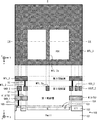
- FIG. 2 is a plan layout view of a basic part of the pixel unit shown in FIG. It is a cross-sectional schematic diagram of the fundamental part of the pixel part shown in FIG.
- FIG. 5 is a plan layout view of the second wiring layer and below of the pixel portion of the CMOS image sensor according to the first embodiment.
- FIG. 6 is a plan layout view of a third wiring layer of the pixel portion of the CMOS image sensor according to the first embodiment.
- FIG. 2 is a schematic cross-sectional view of a pixel portion of the CMOS image sensor according to the first embodiment.
- FIG. 13 is a plan layout view of the second wiring layer and below of the pixel portion of the CMOS image sensor according to the second embodiment.
- FIG. 7 is a plan layout view of a third wiring layer of a pixel portion of a CMOS image sensor according to Embodiment 2.
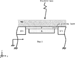
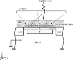
- FIG. 6 is a schematic cross-sectional view of a pixel portion of a CMOS image sensor according to a second embodiment. It is a cross-sectional schematic diagram of an embedded photodiode. It is a figure for demonstrating the subject at the time of irradiating a radiation to the embedded photodiode shown in FIG.
- the constituent elements are not necessarily essential unless specifically stated and when it is considered to be obviously essential in principle.
- the shapes, positional relationships and the like of components etc. when referring to the shapes, positional relationships and the like of components etc., the shapes thereof are substantially the same unless particularly clearly stated and where it is apparently clearly not so in principle. It is assumed that it includes things that are similar or similar to etc. The same applies to the above-described numbers and the like (including the number, the numerical value, the amount, the range, and the like).
- CMOS image sensor solid-state imaging device
- FIG. 10 is a schematic cross-sectional view of the embedded photodiode.
- N-type diffusion region N - region
- the N-type diffusion region is formed by doping the surface of the P well with an N-type impurity.
- a PN junction type photodiode is configured by the P well and the N type diffusion region.
- an element isolation region (STI; Shallow Trench Isolation) is formed at a distance from the N-type diffusion region.
- STI Shallow Trench Isolation
- a P-type pinning layer is formed on the surface of the active region surrounded by the element isolation region, including the surface of the N-type diffusion region. The pinning layer is formed by doping the surface of the active region surrounded by the element isolation region with a P-type impurity.
- a SiO 2 insulating film (PMD; Pre Metal Dielectric) is formed on the surface.
- the ordinary photodiode has no pinning layer, and has a structure in which the surface of the N type diffusion region is directly covered with PMD.
- dark current electrons are generated by thermal excitation in addition to signal electrons excited by an optical signal.
- the output of this dark current electron is better as it approaches 0, and the increase of the dark current causes the deterioration of the image quality.
- the pinning layer is not limited to the case where it is formed by doping a P-type impurity on the surface of the active region.
- the pinning layer may be formed, for example, by applying a negative voltage to the photosensitive region (active region) from the ITO transparent conductive layer formed on the substrate, as disclosed in Patent Document 1 .
- the P-type pinning layer formed on the surface of the embedded photodiode may be inverted to N-type. In that case, the effect of dark current suppression by the pinning layer may be lost.
- CMOS image sensor solid-state imaging device
- Embodiment 1 First, the basic configuration of the pixel portion of the surface-illuminated CMOS image sensor (solid-state image sensor) will be described with reference to FIGS. 1, 2 and 3.
- FIG. 1 the basic configuration of the pixel portion of the surface-illuminated CMOS image sensor (solid-state image sensor) will be described with reference to FIGS. 1, 2 and 3.
- FIG. 1 the basic configuration of the pixel portion of the surface-illuminated CMOS image sensor (solid-state image sensor) will be described with reference to FIGS. 1, 2 and 3.
- FIG. 1 the basic configuration of the pixel portion of the surface-illuminated CMOS image sensor (solid-state image sensor) will be described with reference to FIGS. 1, 2 and 3.
- FIG. 1 is a diagram showing a basic circuit configuration of a pixel unit used in the CMOS image sensor according to the first embodiment.
- the pixel section 1 of the CMOS image sensor shown in FIG. 1 is a pixel section of a typical four-transistor type CMOS image sensor also called a so-called APS (Active Pixel Sensor).
- the pixel unit 1 includes four N-channel MOS transistors TR1 to TR4 and a photodiode PD1.
- the four N-channel MOS transistors TR1 to TR4 are also referred to as a transfer transistor TR1, a reset transistor TR2, an amplification transistor TR3, and a row selection transistor TR4, respectively.
- the anode of the photodiode PD1 is connected to the ground voltage line GND, and the cathode of the photodiode PD1 is connected to the source of the transfer transistor TR1.
- the drain (TR1_D) is connected to the node N1
- the gate (TR1_G) is connected to the transfer gate drive line 4 on which the transfer gate drive signal ⁇ TG propagates.
- the source (TR2_S) is connected to the node N1
- the drain (TR2_D) is connected to the power supply voltage line VDD
- the gate (TR2_G) is connected to the reset signal line 5 on which the reset signal ⁇ R propagates .
- the source (TR3_S) is connected to the node N2
- the drain (TR3_D) is connected to the power supply voltage line VDD
- the gate (TR3_G) is connected to the node N1. That is, the drain of the transfer transistor TR1, the source of the reset transistor TR2, and the gate of the amplification transistor TR3 are connected to each other at the node N1. Further, a floating diffusion layer capacitance FD1 is formed at the node N1.
- row selection transistor TR4 the source (TR4_S) is connected to output signal line VOUT along with a plurality of other pixels provided in the column direction, the drain is connected to node N2, and the gate (TR4_G) is row selection signal ⁇ SEL. Are connected to the propagating row selection signal line 6 of FIG.
- the photodiode PD1 converts the received light signal into an electrical signal.
- the transfer transistor TR1 is turned on when the transfer gate drive signal ⁇ TG becomes active, and transfers the electric signal converted from the light signal by the photodiode PD1 to the node N1. As a result, a charge corresponding to the electrical signal from the photodiode PD1 is accumulated in the floating diffusion layer capacitance FD1 formed at the node N1.
- the amplification transistor TR3 drives the voltage of the node N1 and outputs it to the node N2.
- the row selection transistor TR4 turns on when the row selection signal ⁇ SEL becomes active, and outputs the voltage of the node N2 (ie, the electrical signal converted from the light signal by the photodiode PD1) to the output signal line VOUT.
- FIG. 2 is a plan layout view showing a basic portion of the pixel unit 1 shown in FIG. 1 as a pixel unit 1B.
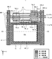
- FIG. 3 is a schematic cross-sectional view of a portion III-III in the plan layout view shown in FIG.
- a rectangular photodiode PD1 is formed in a region that occupies most of the pixel section 1B in plan view, and the metal of the transfer gate driving line 4 is formed so as to surround the outer periphery thereof. .
- transistors TR1 to TR4 are formed in the peripheral region (upper part of the sheet of FIG. 2) on one side of the rectangular photodiode PD1 in plan view. Further, in plan view, the ground voltage line GND, the power supply voltage line VDD and the output signal line VOUT are disposed in parallel with the photodiode PD1 and the transistors TR1 to TR4 interposed therebetween.
- an N-type diffusion region 103 is formed on the surface of a P-well 101 formed in a semiconductor substrate 100.
- the N type diffusion region 103 is formed by doping the surface of the P well 101 with an N type impurity.
- the P well 101 and the N type diffusion region 103 constitute a PN junction type photodiode PD1.
- an element isolation region (STI) 102 is formed spaced apart from the N-type diffusion region 103.
- a P-type pinning layer 104 is formed on the surface of the active region surrounded by the element isolation region 102 including the surface of the N-type diffusion region 103.
- the pinning layer 104 is formed by doping the surface of the active region surrounded by the element isolation region 102 with a P-type impurity.
- the outer periphery of the N-type diffusion region 103 (in other words, the outer periphery of the photodiode PD1) is indicated by a dashed dotted line 11 in FIG. Also, the boundary between the element isolation region 102 and the active region surrounded by it is indicated by a solid line 10 in FIG. However, among the boundaries between the element isolation region 102 and the active region surrounded by the device isolation region 102, the boundaries hidden in the wiring layer are indicated by the broken line 10.
- a P-type diffusion region 105 is formed on the surface of the P well 101 separately from the N-type diffusion region 103.
- the P type diffusion region 105 is formed by doping the surface of the P well 101 with a P type impurity.
- a transparent insulating film 106 (not shown) such as SiO 2 is formed by, eg, CVD (Chemical Vapor Deposition).
- the metal of the transfer gate driving line 4 described above is a photodiode in plan view in the first wiring layer adjacent (closest to) the semiconductor substrate 100. It is formed so as to surround the outer circumference of the PD 1 (the outer circumference of the N-type diffusion region 103). Thereby, stray light can be prevented from entering the photodiode PD1 from the periphery.
- the ground voltage line GND, the power supply voltage line VDD and the output signal line VOUT described above are arranged in parallel with the photodiode PD1 and the transistors TR1 to TR4 interposed therebetween in plan view.
- the ground voltage line GND, the power supply voltage line VDD and the output signal line VOUT arranged in the second wiring layer are also referred to as a ground voltage line GND_2, a power supply voltage line VDD_2 and an output signal line VOUT_2, respectively.
- the ground voltage line GND_2 arranged in the second wiring layer is connected to the ground voltage line GND_1 arranged in the first wiring layer via the via V1.
- the ground voltage line GND_1 arranged in the first wiring layer is connected to the P-type diffusion region 105 via the contact CT1.
- FIG. 4 and FIG. 5 are plan layout views of a configuration in which one of the features of the present invention is added to the basic portion of the pixel section 1 shown in FIG. 4 shows only the first and second wiring layers among the plurality of wiring layers, and FIG. 5 shows only the third wiring layer among the plurality of wiring layers.
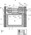
- FIG. 6 is a schematic cross-sectional view of a VI-VI portion of the plan layout views shown in FIGS. 4 and 5.
- the metal electrode MTL is It is further formed.
- metal electrodes MTL_2 and MTL_3 are formed in the second and third wiring layers, respectively, and they are electrically connected by vias V2.
- a metal electrode MTL is configured by the metal electrodes MTL_2 and MTL_3 and the via V2.
- the metal electrode MTL_2 is formed in a ring shape so as to surround the outer periphery of the photodiode PD1 (the outer periphery of the N-type diffusion region 103) in plan view in the second wiring layer.
- the metal electrode MTL_3 is formed to surround the outer periphery of the photodiode PD1 (the outer periphery of the N-type diffusion region 103) in plan view in the third wiring layer. Therefore, the light received by the photodiode PD1 is not blocked by the metal electrodes MTL_2 and MTL_3.
- a negative voltage is applied to the metal electrode MTL (metal electrodes MTL_2 and MTL_3). Therefore, even if fixed positive charges are accumulated in the insulating film 106 by the ionizing action of the total dose effect generated by irradiation of radiation such as gamma rays, an electric field is generated in the photodiode PD1 using the negative voltage of the metal electrode MTL. Thus, the influence of the fixed positive charge to which the pinning layer 104 is subjected can be offset. Thereby, since the function of the pinning layer 104 is maintained, the dark current generated by thermal excitation at the interface between the N-type diffusion region 103 and the insulating film 106 is swept to the ground via the pinning layer 104. As a result, the quality deterioration of the image displayed by the pixel unit 1 is suppressed.
- the distance between the metal electrode MTL and the photodiode PD1 becomes too close. It will In this case, an electric field is generated near the periphery near the metal electrode MTL in the formation region of the photodiode PD1 in plan view, but an electric field is hardly generated at the center. Therefore, in the central portion of the photodiode PD1, the influence of the fixed positive charge received by the pinning layer 104 can not be sufficiently offset. This problem becomes more pronounced as the formation region of the photodiode PD1 increases.
- the metal formed in the wiring layer higher than the first wiring layer is employed as the metal electrode MTL.
- the distance between the metal electrode MTL and the photodiode PD1 is appropriately separated, so that an electric field is generated relatively uniformly not only in the periphery but also in the center of the photodiode PD1 in plan view. Therefore, in the photodiode PD1, the influence of the fixed positive charge received by the pinning layer 104 can be offset over the entire surface.
- the pixel unit 1 of the CMOS image sensor according to the present embodiment can cause the pinning layer 104 to function with high accuracy, so that the increase of dark current can be suppressed, and as a result, the deterioration of the image quality is suppressed. can do.
- a negative voltage is applied to surround the outer periphery of the formation region of the photodiode PD1 in plan view in a layer higher than the first wiring layer.
- the metal electrode MTL is formed.
- the pixel unit 1 of the CMOS image sensor according to the present embodiment can cause the pinning layer 104 to function with high accuracy, so that the increase of dark current can be suppressed, and as a result, the deterioration of the image quality is suppressed. can do.
- the metal electrode MTL is formed in the wiring layer, unlike the case where the ITO transparent conductive layer is formed as disclosed in Patent Document 1, , No special manufacturing process is required. Therefore, it is possible to suppress the manufacturing problems and the increase in the process cost associated with the addition of the ITO transparent electrode.
- the photodiode PD1 has a buried type structure covered in advance with the pinning layer 104
- the photodiode PD1 may have a structure not previously covered with the pinning layer 104.
- a P-type diffusion region corresponding to the pinning layer 104 can be formed on the surface of the N-type diffusion region 103 by increasing the negative voltage applied to the metal electrode MTL.
- the present invention is not limited to this.
- the metal electrode MTL may be formed only in one wiring layer higher than the first wiring layer, or may be formed across three or more wiring layers higher than the first wiring layer.
- Second Embodiment 7 and 8 are plan layout views of the pixel section 2 of the surface-illuminated CMOS image sensor according to the second embodiment. 7 shows only the first and second wiring layers among the plurality of wiring layers, and FIG. 8 shows only the third wiring layer among the plurality of wiring layers.
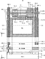
- FIG. 9 is a schematic cross-sectional view of a portion IX-IX in the plan layout views shown in FIGS. 7 and 8.
- the pixel unit 2 further includes a metal electrode MTL_2a in comparison with the pixel unit 1.
- the metal electrode MTL_2a is formed to overlap a part of the formation region of the photodiode PD1 in plan view in the second wiring layer.
- the metal electrode MTL_2a is formed in a band shape from one side of the metal electrode MTL2 to the other side opposed to the central portion of the formation region of the photodiode PD1 in plan view in the second wiring layer .
- the metal electrode MTL_2a is electrically connected to the metal electrode MTL_2. Therefore, a negative voltage is also applied to the metal electrode MTL_2a.
- the other structure of the pixel unit 2 is the same as that of the pixel unit 1, and thus the description thereof is omitted.
- a negative voltage is applied to surround the outer periphery of the formation region of the photodiode PD1 in plan view in a layer higher than the first wiring layer.
- the metal electrode MTL is formed.
- the pixel unit 2 of the CMOS image sensor according to the present embodiment can cause the pinning layer 104 to function with high accuracy, so that the increase of dark current can be suppressed, and as a result, the deterioration of the image quality is suppressed. can do.
- the pixel unit 2 of the CMOS image sensor in a layer higher than the first wiring layer, it overlaps with a part (in particular, the central part) of the formation region of the photodiode PD1 in plan view.
- a metal electrode MTL_2a to which a negative voltage is applied is formed.
- the pixel unit 2 can generate a strong electric field not only in the peripheral portion of the top surface of the photodiode PD1 but also in the central portion. That is, the pixel unit 2 can generate an electric field more uniformly over the entire top surface of the photodiode PD1.
- the pixel unit 2 can more accurately offset the influence of the fixed positive charge that the pinning layer 104 receives.
- the pixel section 2 of the CMOS image sensor according to the present embodiment can function the pinning layer 104 more accurately, and therefore, the increase in dark current can be further suppressed, and as a result, the image quality is degraded. Can be further suppressed.
- the present invention is not limited thereto.
- a single metal electrode MTL_2a may be provided. Even in such a case, by forming the metal electrode MTL_2a in the wiring layer higher than the first wiring layer, the distance between the metal electrode MTL_2a and the photodiode PD1 can be appropriately separated, so the photodiode PD1 is formed. An electric field can be generated relatively uniformly over the entire top surface.
- the metal electrode MTL_2a is formed so as to overlap with a part of the formation region of the photodiode PD1 in plan view, but the metal electrode MTL_2a has another narrowest wiring width.
- the metal electrode MTL_2a is formed in a band shape from one side of the formation region of the rectangular photodiode PD1 to the other side opposed in plan view, but the present invention is not limited thereto.
- the metal electrode MTL_2a may have any shape as long as it can generate an electric field uniformly over the entire upper surface of the photodiode PD1 and can suppress the decrease in sensitivity of the photodiode PD1 due to light shielding within an acceptable range. Good.
- the metal electrode MTL_2a may be disposed in any wiring layer as long as it is a layer higher than the first wiring layer.
- the photodiode PD1 has a buried type structure covered in advance with the pinning layer 104
- the present invention is not limited thereto.
- the photodiode PD1 may have a structure not previously covered with the pinning layer 104.
- a P-type diffusion region corresponding to the pinning layer 104 can be formed on the surface of the N-type diffusion region 103 by increasing the negative voltage applied to the metal electrode MTL.
- the conductivity type of each MOS transistor may be replaced with P-type to N-type and N-type to P-type, respectively.
- the present invention can be suitably applied to a solid-state imaging device used for a high-performance camera.
Landscapes
- Engineering & Computer Science (AREA)
- Multimedia (AREA)
- Signal Processing (AREA)
- Solid State Image Pick-Up Elements (AREA)
- Transforming Light Signals Into Electric Signals (AREA)
- Light Receiving Elements (AREA)
Abstract
一実施の形態によれば、固体撮像素子は、半導体基板(100)と、半導体基板(100)の表面に形成されたPN接合型のフォトダイオード(PD1)と、フォトダイオード(PD1)の形成面上を含む半導体基板(100)の表面上に形成された絶縁膜(106)と、絶縁膜(106)上に積層された複数の配線層のうち、フォトダイオード(PD1)に隣接する第1配線層よりも上位階層の配線層に形成され、かつ、負電圧が印加されたメタル電極(MTL)と、を備える。
Description
本発明は、固体撮像素子及びその形成方法に関し、例えば放射線の照射に起因して生じる画質の劣化を防ぐのに適した固体撮像素子及びその形成方法に関する。
近年、宇宙技術分野、原子力分野等では、高性能カメラの運用が期待されている。例えば、特許文献1には、高性能カメラに用いられる固体撮像素子に関する技術が開示されている。
特許文献1に開示された感光素子(固体撮像素子)は、半導体基板に形成されたPウェル及びその表面に形成されたN型の感光領域からなるフォトダイオードと、感光領域の表面に形成された透明絶縁層と、透明絶縁層の表面に形成されたインジウム錫酸化物(ITO)からなる透明導電層と、を備える。さらに、この感光素子は、透明導電層から感光領域に対して負電圧を印加することにより、感光領域の表面にP型のピン止め層(ピニング層)を形成している。それにより、この感光素子は、感光領域と透明絶縁層との界面において熱励起により発生した暗電流を、ピン止め層を経由してグランドに掃引することができるため、画像の品質を向上させることができる。
しかしながら、宇宙空間、原子力施設、放射線施設内等で用いられる電子機器では、通常環境とは異なり、ガンマ線等の放射線の照射によって発生するトータルドーズ効果の電離作用によって、絶縁膜中に固定正電荷が蓄積されるため、その影響で諸特性が劣化してしまうという問題があった。
具体的には、特許文献1に開示された感光素子の構成では、放射線の照射によって発生するトータルドーズ効果の電離作用によって、透明絶縁層に固定正電荷が蓄積されるため、その影響でP型のピン止め層がN型に反転してしまい、当該ピン止め層が正常に機能しなくなってしまう。その結果、この感光素子では、感光領域と透明絶縁層との界面において暗電流が蓄積されてしまうため、ホワイトアウト等の画質の劣化が発生してしまうという問題があった。その他の課題と新規な特徴は、本明細書の記述および添付図面から明らかになるであろう。
一実施の形態によれば、固体撮像素子は、半導体基板と、前記半導体基板の表面に形成されたPN接合型のフォトダイオードと、前記フォトダイオードの形成面上を含む前記半導体基板の表面上に形成された絶縁膜と、前記絶縁膜上に積層された複数の配線層のうち、前記フォトダイオードに隣接する第1配線層よりも上位階層の配線層に形成され、かつ、負電圧が印加された第1メタル電極と、を備える。
また、一実施の形態によれば、固体撮像素子の形成方法は、半導体基板の表面にPN接合型のフォトダイオードを形成し、前記フォトダイオードの形成面上を含む前記半導体基板の表面上に絶縁膜を形成し、前記絶縁膜上に積層される複数の配線層のうち、前記フォトダイオードに隣接する第1配線層よりも上位階層の配線層に第1メタル電極を形成し、前記第1メタル電極に負電圧を印加する。
前記一実施の形態によれば、固体撮像素子及びその形成方法に関し、例えば放射線の照射に起因して生じる画質の劣化を防ぐのに適した固体撮像素子及びその形成方法を提供することができる。
以下、図面を参照しつつ、実施の形態について説明する。なお、図面は簡略的なものであるから、この図面の記載を根拠として実施の形態の技術的範囲を狭く解釈してはならない。また、同一の要素には、同一の符号を付し、重複する説明は省略する。
以下の実施の形態においては便宜上その必要があるときは、複数のセクションまたは実施の形態に分割して説明するが、特に明示した場合を除き、それらはお互いに無関係なものではなく、一方は他方の一部または全部の変形例、応用例、詳細説明、補足説明等の関係にある。また、以下の実施の形態において、要素の数等(個数、数値、量、範囲等を含む)に言及する場合、特に明示した場合および原理的に明らかに特定の数に限定される場合等を除き、その特定の数に限定されるものではなく、特定の数以上でも以下でもよい。
さらに、以下の実施の形態において、その構成要素(動作ステップ等も含む)は、特に明示した場合および原理的に明らかに必須であると考えられる場合等を除き、必ずしも必須のものではない。同様に、以下の実施の形態において、構成要素等の形状、位置関係等に言及するときは、特に明示した場合および原理的に明らかにそうでないと考えられる場合等を除き、実質的にその形状等に近似または類似するもの等を含むものとする。このことは、上記数等(個数、数値、量、範囲等を含む)についても同様である。
<発明者らによる事前検討>
実施の形態1にかかるCMOSイメージセンサ(固体撮像素子)について説明する前に、まず、一般的な表面照射型CMOSイメージセンサに設けられた埋め込みフォトダイオードについて説明する。
実施の形態1にかかるCMOSイメージセンサ(固体撮像素子)について説明する前に、まず、一般的な表面照射型CMOSイメージセンサに設けられた埋め込みフォトダイオードについて説明する。
図10は、埋め込みフォトダイオードの断面模式図である。
図10に示すように、シリコン基板に形成されたPウェルの表面には、N型拡散領域(N-領域)が形成されている。このN型拡散領域は、Pウェルの表面にN型不純物をドーピングすることにより形成されている。ここで、PウェルとN型拡散領域とによってPN接合型のフォトダイオードが構成されている。
図10に示すように、シリコン基板に形成されたPウェルの表面には、N型拡散領域(N-領域)が形成されている。このN型拡散領域は、Pウェルの表面にN型不純物をドーピングすることにより形成されている。ここで、PウェルとN型拡散領域とによってPN接合型のフォトダイオードが構成されている。
また、Pウェルの表面には、N型拡散領域と間隔を空けて、素子分離領域(STI;Shallow Trench Isolation)が形成されている。また、N型拡散領域の表面を含む、素子分離領域に囲まれた活性領域の表面には、P型のピニング層が形成されている。このピニング層は、素子分離領域に囲まれた活性領域の表面にP型不純物をドーピングすることにより形成されている。さらに、その表面には、SiO2絶縁膜(PMD;Pre Metal Dielectric)が形成されている。
なお、通常のフォトダイオードは、図10に示す埋め込みフォトダイオードのうち、ピニング層を持たず、N型拡散領域の表面が直接PMDで覆われた構造を有している。
固体撮像素子に用いられるフォトダイオードでは、通常、光信号によって励起された信号電子に加えて、熱励起による暗電流電子が生成される。この暗電流電子の出力は0に近いほどよく、暗電流の増大は、画質の劣化を生じさせる。
例えば、ピニング層を持たない通常のフォトダイオードの場合、N型拡散領域とPMDとの界面にダングリングボンドや結晶欠陥が多数存在するため、バンド構造の禁制帯領域に欠陥準位が生じてしまう。その結果、熱励起によって生成される暗電流電子が増加して、暗電流が増大してしまう。それに対し、ピニング層を持つ埋め込みフォトダイオードの場合、熱励起によって生成された暗電流電子は、P型のピニング層及びPウェルを伝搬してグランドに掃引される。それにより、暗電流の増大が抑制されるため、画像の品質劣化は抑制される。
なお、ピニング層は、活性領域の表面にP型不純物のドーピングすることにより形成される場合に限られない。ピニング層は、例えば、特許文献1に開示されているように、基板上に形成されたITO透明導電層から感光領域(活性領域)に対して負電圧を印加することにより形成されることもある。
続いて、図11を用いて、図10に示す埋め込みフォトダイオードが宇宙空間、原子力施設、放射線施設内等で用いられた場合の課題について説明する。
図11に示すように、ガンマ線等の放射線が埋め込みフォトダイオードに照射された場合、放射線の照射によって発生するトータルドーズ効果の電離作用により、絶縁体であるPMD中に電荷が生成される。この電荷のうち、負電荷である電子は、移動度が高いため、比較的短い時間で電極側に掃引され、電極において消滅する。それに対し、正電荷である正孔は、負電荷よりも移動度が低いため、PMD中に取り残されてしまう。この正電荷は、徐々にPMD外に掃引されるが、その過程において、PMDとシリコン基板との界面近傍に存在する欠陥にトラップされ、固定正電荷となる。このように、PMDとシリコン基板との界面近傍に固定正電荷が発生すると、埋め込みフォトダイオードの表面に形成されたP型のピニング層がN型に反転してしまう可能性がある。その場合、ピニング層による暗電流抑制の効果が無くなってしまう可能性がある。
そこで、発明者らは、ピニング層の機能を失わせることなく、放射線の照射に起因して生じる画質の劣化を防ぐことが可能な、実施の形態1にかかるCMOSイメージセンサ(固体撮像素子)を見出した。
<実施の形態1>
まず、図1、図2及び図3を用いて、表面照射型CMOSイメージセンサ(固体撮像素子)の画素部の基本構成を説明する。
まず、図1、図2及び図3を用いて、表面照射型CMOSイメージセンサ(固体撮像素子)の画素部の基本構成を説明する。
(CMOSイメージセンサの画素部1の基本的な回路構成)
図1は、実施の形態1に係るCMOSイメージセンサに用いられる画素部の基本的な回路構成を示す図である。図1に示すCMOSイメージセンサの画素部1は、所謂、APS(Active Pixel Sensor)とも呼ばれる典型的な4トランジスタ型CMOSイメージセンサの画素部である。
図1は、実施の形態1に係るCMOSイメージセンサに用いられる画素部の基本的な回路構成を示す図である。図1に示すCMOSイメージセンサの画素部1は、所謂、APS(Active Pixel Sensor)とも呼ばれる典型的な4トランジスタ型CMOSイメージセンサの画素部である。
図1に示すように、画素部1は、4つのNチャネルMOSトランジスタTR1~TR4と、フォトダイオードPD1と、を備える。以下、4つのNチャネルMOSトランジスタTR1~TR4を、それぞれ、トランスファトランジスタTR1、リセットトランジスタTR2、増幅トランジスタTR3、及び、行選択トランジスタTR4とも称す。
フォトダイオードPD1のアノードは、接地電圧線GNDに接続され、フォトダイオードPD1のカソードは、トランスファトランジスタTR1のソースに接続されている。トランスファトランジスタTR1では、ドレイン(TR1_D)がノードN1に接続され、ゲート(TR1_G)が、転送ゲート駆動信号φTGの伝搬する転送ゲート駆動ライン4に接続されている。
リセットトランジスタTR2では、ソース(TR2_S)がノードN1に接続され、ドレイン(TR2_D)が電源電圧線VDDに接続され、ゲート(TR2_G)が、リセット信号φRの伝搬するリセット信号線5に接続されている。
増幅トランジスタTR3では、ソース(TR3_S)がノードN2に接続され、ドレイン(TR3_D)が電源電圧線VDDに接続され、ゲート(TR3_G)がノードN1に接続されている。つまり、トランスファトランジスタTR1のドレイン、リセットトランジスタTR2のソース、及び、増幅トランジスタTR3のゲートは、ノードN1において互いに接続されている。また、ノードN1には、浮遊拡散層容量FD1が形成されている。
行選択トランジスタTR4では、ソース(TR4_S)が、列方向に設けられた他の複数の画素とともに出力信号線VOUTに接続され、ドレインがノードN2に接続され、ゲート(TR4_G)が、行選択信号φSELの伝搬する行選択信号線6に接続されている。
フォトダイオードPD1は、受光した光信号を電気信号に変換する。トランスファトランジスタTR1は、転送ゲート駆動信号φTGがアクティブになった場合にオンし、フォトダイオードPD1によって光信号から変換された電気信号をノードN1に転送する。それにより、ノードN1に形成された浮遊拡散層容量FD1には、フォトダイオードPD1からの電気信号に応じた電荷が蓄積される。増幅トランジスタTR3は、ノードN1の電圧をドライブしてノードN2に出力する。行選択トランジスタTR4は、行選択信号φSELがアクティブになった場合にオンし、ノードN2の電圧(即ち、フォトダイオードPD1によって光信号から変換された電気信号)を、出力信号線VOUTに出力する。
(画素部1の基本的部分の平面レイアウト図及び断面模式図)
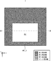
図2は、図1に示す画素部1の基本的部分を画素部1Bとして示す平面レイアウト図である。図3は、図2に示す平面レイアウト図のIII-III部分の断面模式図である。
図2は、図1に示す画素部1の基本的部分を画素部1Bとして示す平面レイアウト図である。図3は、図2に示す平面レイアウト図のIII-III部分の断面模式図である。
図2に示すように、平面視上、画素部1Bの大部分を占める領域に、矩形状のフォトダイオードPD1が形成され、その外周を囲むようにして、転送ゲート駆動ライン4のメタルが形成されている。
また、平面視上、矩形状のフォトダイオードPD1の一辺側の周辺領域(図2の紙面の上部)には、4つのトランジスタTR1~TR4が形成されている。さらに、平面視上、フォトダイオードPD1及びトランジスタTR1~TR4を挟むようにして、接地電圧線GNDと、電源電圧線VDD及び出力信号線VOUTと、が並行に配置されている。
図3に示すように、半導体基板100に形成されたPウェル101の表面には、N型拡散領域103が形成されている。このN型拡散領域103は、Pウェル101の表面にN型不純物をドーピングすることにより形成されている。ここで、Pウェル101とN型拡散領域103とによってPN接合型のフォトダイオードPD1が構成されている。
また、Pウェル101の表面には、N型拡散領域103と間隔を空けて、素子分離領域(STI)102が形成されている。N型拡散領域103の表面を含む、素子分離領域102に囲まれた活性領域の表面には、P型のピニング層104が形成されている。このピニング層104は、素子分離領域102に囲まれた活性領域の表面にP型不純物をドーピングすることにより形成されている。
なお、N型拡散領域103の外周辺(換言すると、フォトダイオードPD1の外周辺)は、図2において一点鎖線11で示されている。また、素子分離領域102とそれに囲まれた活性領域との境界線は、図2において実線10で示されている。ただし、素子分離領域102とそれに囲まれた活性領域との境界線のうち、配線層に隠れている境界線については、破線10で示されている。
また、Pウェル101の表面には、N型拡散領域103と分離してP型拡散領域105が形成されている。このP型拡散領域105は、Pウェル101の表面にP型不純物をドーピングすることにより形成される。
さらに、半導体基板100の表面には、例えばCVD(Chemical Vapor Deposition)法によって、SiO2等の透明の絶縁膜106(不図示)が形成されている。
この絶縁膜上に積層された複数の配線層のうち、半導体基板100に隣接する(最も近接する)第1配線層には、前述した転送ゲート駆動ライン4のメタルが、平面視上、フォトダイオードPD1の外周(N型拡散領域103の外周)を囲むようにして形成されている。それにより、周辺からフォトダイオードPD1に迷光が入り込むのを防ぐことができる。
また、第2配線層には、前述した、接地電圧線GNDと、電源電圧線VDD及び出力信号線VOUTとが、平面視上、フォトダイオードPD1及びトランジスタTR1~TR4を挟むようにして並列に配置されている。なお、第2配線層に配置された接地電圧線GND、電源電圧線VDD及び出力信号線VOUTを、それぞれ、接地電圧線GND_2、電源電圧線VDD_2及び出力信号線VOUT_2とも称す。図3の例では、第2配線層に配置された接地電圧線GND_2は、ビアV1を介して、第1配線層に配置された接地電圧線GND_1に接続されている。そして、第1配線層に配置された接地電圧線GND_1は、コンタクトCT1を介して、P型拡散領域105に接続されている。
(本発明の特徴部分が追加された画素部1の平面レイアウト図及び断面模式図)
図4及び図5は、図2に示す画素部1の基本的部分に対し、本発明の特徴の一つを追加した構成の平面レイアウト図である。なお、図4では、複数の配線層のうち第1及び第2配線層のみが示されており、図5では、複数の配線層のうち第3配線層のみが示されている。図6は、図4及び図5に示す平面レイアウト図のVI-VI部分の断面模式図である。
図4及び図5は、図2に示す画素部1の基本的部分に対し、本発明の特徴の一つを追加した構成の平面レイアウト図である。なお、図4では、複数の配線層のうち第1及び第2配線層のみが示されており、図5では、複数の配線層のうち第3配線層のみが示されている。図6は、図4及び図5に示す平面レイアウト図のVI-VI部分の断面模式図である。
図4~図6に示すように、画素部1は、図2に示す画素部1Bと比較して、複数の配線層のうち、第1配線層より上位階層の配線層において、メタル電極MTLがさらに形成されている。本例では、第2及び第3配線層のそれぞれにメタル電極MTL_2,MTL_3が形成され、それらがビアV2によって電気的に接続されている。これらメタル電極MTL_2,MTL_3及びビアV2によってメタル電極MTLが構成されている。
メタル電極MTL_2は、第2配線層において、平面視上、フォトダイオードPD1の外周(N型拡散領域103の外周)を囲むようにしてリング状に形成されている。また、メタル電極MTL_3は、第3配線層において、平面視上、フォトダイオードPD1の外周(N型拡散領域103の外周)を囲むようにして形成されている。そのため、フォトダイオードPD1の受ける光がメタル電極MTL_2,MTL_3によって遮られることはない。
ここで、メタル電極MTL(メタル電極MTL_2,MTL_3)には、負電圧が印加されている。そのため、ガンマ線等の放射線の照射によって発生するトータルドーズ効果の電離作用によって、絶縁膜106に固定正電荷が蓄積された場合でも、メタル電極MTLの負電圧を用いてフォトダイオードPD1に電界を生じさせることにより、ピニング層104が受ける固定正電荷の影響を相殺させることができる。それにより、ピニング層104の機能が維持されるため、N型拡散領域103と絶縁膜106との界面において熱励起により発生した暗電流は、ピニング層104を経由してグランドに掃引される。その結果、画素部1によって表示される画像の品質劣化が抑制される。
なお、仮に、MOSトランジスタのゲート電極等に用いられるポリシリコンや、第1配線層に形成されるメタルを、メタル電極MTLとして採用した場合、メタル電極MTLとフォトダイオードPD1と間の距離が近づきすぎてしまう。この場合、平面視上、フォトダイオードPD1の形成領域のうち、メタル電極MTLに近い周辺部近傍には電界が生成されるが、中央部に電界がほとんど生成されない。そのため、フォトダイオードPD1の中央部では、ピニング層104が受ける固定正電荷の影響を十分に相殺することができない。この問題は、フォトダイオードPD1の形成領域が大きくなるほど顕著になる。
それに対し、本実施の形態にかかるCMOSイメージセンサの画素部1では、第1配線層より上位階層の配線層に形成されるメタルを、メタル電極MTLとして採用している。それにより、メタル電極MTLとフォトダイオードPD1との間の距離が適度に離れるため、平面視上、フォトダイオードPD1の周辺部のみならず中央部にも比較的均一に電界が生成される。そのため、フォトダイオードPD1では、全面にわたって、ピニング層104が受ける固定正電荷の影響を相殺することができる。それにより、本実施の形態にかかるCMOSイメージセンサの画素部1は、ピニング層104を精度良く機能させることができるため、暗電流の増大を抑制することができ、その結果、画質の劣化を抑制することができる。
このように、実施の形態1に係るCMOSイメージセンサの画素部1では、第1配線層よりも上位階層において、平面視上、フォトダイオードPD1の形成領域の外周を囲むようにして、負電圧の印加されたメタル電極MTLが形成されている。それにより、画素部1は、放射線の照射によって発生するトータルドーズ効果の電離作用によって絶縁膜106に固定正電荷が蓄積された場合でも、メタル電極MTLの負電圧を用いてフォトダイオードPD1に電界を生じさせることにより、ピニング層104が受ける固定正電荷の影響を相殺させることができる。それにより、本実施の形態にかかるCMOSイメージセンサの画素部1は、ピニング層104を精度良く機能させることができるため、暗電流の増大を抑制することができ、その結果、画質の劣化を抑制することができる。
なお、本実施の形態にかかるCMOSイメージセンサの画素部1では、配線層にメタル電極MTLを形成しているため、特許文献1に開示されているようにITO透明導電層を形成する場合と異なり、特殊な製造プロセスは不要である。そのため、製造上の問題やITO透明電極追加に伴うプロセスコストの増大を抑制することができる。
本実施の形態では、フォトダイオードPD1が、ピニング層104で予め覆われた埋め込み型の構造である場合を例に説明したが、これに限られない。フォトダイオードPD1は、ピニング層104で予め覆われていない構造であってもよい。この場合、メタル電極MTLに印加される負電圧を大きくすることによって、N型拡散領域103の表面に、ピニング層104に相当するP型拡散領域を形成することができる。
また、本実施の形態では、メタル電極MTLが2つの配線層に跨って形成された場合を例に説明したが、これに限られない。メタル電極MTLは、第1配線層より上位階層の一つの配線層にのみ形成されてもよいし、第1配線層より上位階層の3つ以上の配線層に跨って形成されてもよい。
<実施の形態2>
図7及び図8は、実施の形態2に係る表面照射型CMOSイメージセンサの画素部2の平面レイアウト図である。なお、図7では、複数の配線層のうち第1及び第2配線層のみが示されており、図8では、複数の配線層のうち第3配線層のみが示されている。図9は、図7及び図8に示す平面レイアウト図のIX-IX部分の断面模式図である。
図7及び図8は、実施の形態2に係る表面照射型CMOSイメージセンサの画素部2の平面レイアウト図である。なお、図7では、複数の配線層のうち第1及び第2配線層のみが示されており、図8では、複数の配線層のうち第3配線層のみが示されている。図9は、図7及び図8に示す平面レイアウト図のIX-IX部分の断面模式図である。
図7~図9に示すように、画素部2は、画素部1と比較して、メタル電極MTL_2aをさらに備える。メタル電極MTL_2aは、第2配線層において、平面視上、フォトダイオードPD1の形成領域の一部と重なるように形成されている。本例では、メタル電極MTL_2aは、第2配線層において、平面視上、フォトダイオードPD1の形成領域の中央部と重なるように、メタル電極MTL2の一辺から対向する他辺にかけて帯状に形成されている。また、メタル電極MTL_2aは、メタル電極MTL_2と電気的に接続されている。そのため、メタル電極MTL_2aにも負電圧が印加されている。
画素部2のその他の構造については、画素部1の場合と同様であるため、その説明を省略する。
このように、実施の形態2に係るCMOSイメージセンサの画素部2では、第1配線層よりも上位階層において、平面視上、フォトダイオードPD1の形成領域の外周を囲むようにして、負電圧の印加されたメタル電極MTLが形成されている。それにより、画素部2は、放射線の照射によって発生するトータルドーズ効果の電離作用によって絶縁膜106に固定正電荷が蓄積された場合でも、メタル電極MTLの負電圧を用いてフォトダイオードPD1に電界を生じさせることにより、ピニング層104が受ける固定正電荷の影響を相殺させることができる。それにより、本実施の形態にかかるCMOSイメージセンサの画素部2は、ピニング層104を精度良く機能させることができるため、暗電流の増大を抑制することができ、その結果、画質の劣化を抑制することができる。
さらに、本実施の形態にかかるCMOSイメージセンサの画素部2では、第1配線層よりも上位階層において、平面視上、フォトダイオードPD1の形成領域の一部(特に中央部)と重なるようにして、負電圧の印加されたメタル電極MTL_2aが形成されている。それにより、画素部2は、フォトダイオードPD1上面の周辺部のみならず中央部にも強い電界を生じさせることができる。つまり、画素部2は、フォトダイオードPD1上面の全面にわたってより均一に電界を生じさせることができる。それにより、画素部2は、ピニング層104が受ける固定正電荷の影響をより高精度に相殺させることができる。それにより、本実施の形態にかかるCMOSイメージセンサの画素部2は、ピニング層104をより精度良く機能させることができるため、暗電流の増大をさらに抑制することができ、その結果、画質の劣化をさらに抑制することができる。
なお、本実施の形態では、メタル電極MTLとして、メタル電極MTL_2,MTL_3に加えてメタル電極MTL_2aが設けられている場合について説明したが、これに限られない。メタル電極MTLとして、メタル電極MTL_2a単体が設けられていてもよい。その場合でも、メタル電極MTL_2aを、第1配線層よりも上位階層の配線層に形成することにより、メタル電極MTL_2aとフォトダイオードPD1との間の距離を適度に離すことができるため、フォトダイオードPD1上面の全面にわたって比較的均一に電界を生じさせることができる。
また、本実施の形態では、平面視上、メタル電極MTL_2aがフォトダイオードPD1の形成領域の一部と重なるように形成されているが、メタル電極MTL_2aの幅を、他の最も細い配線幅を有するメタル配線の配線幅に対応する幅とすることにより(具体的には、プロセスルール上の最小寸法とすることにより)、遮光によるフォトダイオードPD1の感度低下の影響は最小限に抑えられる。
また、本実施の形態では、平面視上、メタル電極MTL_2aが矩形状のフォトダイオードPD1の形成領域の一辺から対向する他辺にかけて帯状に形成されているが、これに限られない。メタル電極MTL_2aは、フォトダイオードPD1上面の全面にわたって均一に電界を生じさせることができ、かつ、遮光によるフォトダイオードPD1の感度低下を許容範囲に抑えられるのであれば、どのような形状であってもよい。また、メタル電極MTL_2aは、第1配線層よりも上位階層であればどの配線層に配置されてもよい。
さらに、本実施の形態では、フォトダイオードPD1が、ピニング層104で予め覆われた埋め込み型の構造である場合を例に説明したが、これに限られない。フォトダイオードPD1は、ピニング層104で予め覆われていない構造であってもよい。この場合、メタル電極MTLに印加された負電圧を大きくすることによって、N型拡散領域103の表面に、ピニング層104に相当するP型拡散領域を形成することができる。
以上、本発明者によってなされた発明を実施の形態に基づき具体的に説明したが、本発明は既に述べた実施の形態に限定されるものではなく、その要旨を逸脱しない範囲において種々の変更が可能であることはいうまでもない。例えば、各MOSトランジスタの導電型は、P型からN型、N型からP型にそれぞれ置き換えられてもよい。
この出願は、2017年11月14日に出願された日本出願特願2017-219194を基礎とする優先権を主張し、その開示の全てをここに取り込む。
本発明は、高性能カメラに用いられる固体撮像素子に好適に適用することができる。
1,2 画素部
1B 画素部の基本的部分
4 転送ゲート駆動ライン
5 リセット信号線
6 行選択信号線
10 素子分離領域とそれに囲まれた活性領域との境界線
11 N型拡散領域の外周辺
100 半導体基板
101 Pウェル
102 素子分離領域
103 N型拡散領域
104 ピニング層
105 P型拡散領域
106 絶縁膜
CT1 コンタクト
FD1 浮遊拡散容量
MTL メタル電極
MTL_1 第1層に配線されたメタル電極
MTL_2 第2層に配線されたメタル電極
MTL_2a 第2層に配置された追加メタル電極
N1,N2 ノード
PD1 フォトダイオード
TR1 トランスファトランジスタ
TR2 リセットトランジスタ
TR3 増幅トランジスタ
TR4 行選択トランジスタ
GND 接地電圧線
GND_1 第1層に配線された接地電圧線
GND_2 第2層に配線された接地電圧線
V1,V2 ビア
VDD 電源電圧線
VDD_2 第2層に配線された電源電圧線
VOUT 出力信号線
VOUT_2 第2層に配線された出力信号線
1B 画素部の基本的部分
4 転送ゲート駆動ライン
5 リセット信号線
6 行選択信号線
10 素子分離領域とそれに囲まれた活性領域との境界線
11 N型拡散領域の外周辺
100 半導体基板
101 Pウェル
102 素子分離領域
103 N型拡散領域
104 ピニング層
105 P型拡散領域
106 絶縁膜
CT1 コンタクト
FD1 浮遊拡散容量
MTL メタル電極
MTL_1 第1層に配線されたメタル電極
MTL_2 第2層に配線されたメタル電極
MTL_2a 第2層に配置された追加メタル電極
N1,N2 ノード
PD1 フォトダイオード
TR1 トランスファトランジスタ
TR2 リセットトランジスタ
TR3 増幅トランジスタ
TR4 行選択トランジスタ
GND 接地電圧線
GND_1 第1層に配線された接地電圧線
GND_2 第2層に配線された接地電圧線
V1,V2 ビア
VDD 電源電圧線
VDD_2 第2層に配線された電源電圧線
VOUT 出力信号線
VOUT_2 第2層に配線された出力信号線
Claims (14)
- 半導体基板と、
前記半導体基板の表面に形成されたPN接合型のフォトダイオードと、
前記フォトダイオードの形成面上を含む前記半導体基板の表面上に形成された絶縁膜と、
前記絶縁膜上に積層された複数の配線層のうち、前記フォトダイオードに隣接する第1配線層よりも上位階層の配線層に形成され、かつ、負電圧が印加された第1メタル電極と、
を備えた、固体撮像素子。 - 前記第1メタル電極は、平面視上、前記フォトダイオードの形成領域の外周を囲むように形成されている、
請求項1に記載の固体撮像素子。 - 前記第1メタル電極は、
前記複数の配線層のうち、前記第1配線層よりも上位階層の2以上の配線層において形成されている、
請求項1又は2に記載の固体撮像素子。 - 前記第1メタル電極は、
前記2以上の配線層間に設けられたビアを含む、
請求項3に記載の固体撮像素子。 - 前記複数の配線層のうち前記第1配線層よりも上位階層の配線層において、平面視上、前記フォトダイオードの形成領域の一部と重なるように形成され、かつ、前記第1メタル電極と電気的に接続された第2メタル電極をさらに備えた、
請求項1~4の何れか一項に記載の固体撮像素子。 - 前記第2メタル電極は、平面視上、前記フォトダイオードの形成領域の中央部と重なるように形成されている、
請求項5に記載の固体撮像素子。 - 前記第2メタル電極は、平面視上、矩形状の前記フォトダイオードの形成領域の一辺から前記中央部を通過して対向する他辺にかけて帯状に形成され、
前記第2メタル電極は、他の最も細い配線幅を有するメタル配線の配線幅、に対応する帯幅となるように形成されている、
請求項6に記載の固体撮像素子。 - 前記第1メタル電極は、平面視上、前記フォトダイオードの形成領域の一部と重なるように形成されている、
請求項1に記載の固体撮像素子。 - 前記第1メタル電極は、平面視上、前記フォトダイオードの形成領域の中央部と重なるように形成されている、
請求項8に記載の固体撮像素子。 - 前記第1メタル電極は、平面視上、他の最も細い配線幅を有するメタル配線の配線幅、に対応する帯幅を有するように帯状に形成されている、
請求項9に記載の固体撮像素子。 - 前記フォトダイオードは、
前記半導体基板に形成された一方の導電型のウェルと、
前記ウェル上に形成された他方の導電型の拡散領域と、によって構成される、
請求項1~10の何れか一項に記載の固体撮像素子。 - 前記フォトダイオードは、
前記半導体基板に形成された一方の導電型のウェルと、
前記ウェル上に形成された他方の導電型の拡散領域と、
前記拡散領域の表面に形成された一方の導電型のピニング層と、によって構成される、
請求項1~10の何れか一項に記載の固体撮像素子。 - 前記第1配線層において、平面視上、前記フォトダイオードの形成領域の外周を囲むように形成され、かつ、前記第1メタル電極と電気的に分離して形成されたメタル配線をさらに備えた、
請求項1~12の何れか一項に記載の固体撮像素子。 - 半導体基板の表面にPN接合型のフォトダイオードを形成し、
前記フォトダイオードの形成面上を含む前記半導体基板の表面上に絶縁膜を形成し、
前記絶縁膜上に積層される複数の配線層のうち、前記フォトダイオードに隣接する第1配線層よりも上位階層の配線層に第1メタル電極を形成し、
前記第1メタル電極に負電圧を印加する、
固体撮像素子の形成方法。
Applications Claiming Priority (2)
| Application Number | Priority Date | Filing Date | Title |
|---|---|---|---|
| JP2017-219194 | 2017-11-14 | ||
| JP2017219194A JP7078919B2 (ja) | 2017-11-14 | 2017-11-14 | 固体撮像素子及びその形成方法 |
Publications (1)
| Publication Number | Publication Date |
|---|---|
| WO2019097971A1 true WO2019097971A1 (ja) | 2019-05-23 |
Family
ID=66540125
Family Applications (1)
| Application Number | Title | Priority Date | Filing Date |
|---|---|---|---|
| PCT/JP2018/039594 Ceased WO2019097971A1 (ja) | 2017-11-14 | 2018-10-25 | 固体撮像素子及びその形成方法 |
Country Status (2)
| Country | Link |
|---|---|
| JP (1) | JP7078919B2 (ja) |
| WO (1) | WO2019097971A1 (ja) |
Families Citing this family (1)
| Publication number | Priority date | Publication date | Assignee | Title |
|---|---|---|---|---|
| CN110930356B (zh) * | 2019-10-12 | 2023-02-28 | 上海交通大学 | 一种工业二维码无参考质量评估系统及方法 |
Citations (3)
| Publication number | Priority date | Publication date | Assignee | Title |
|---|---|---|---|---|
| WO2012117931A1 (ja) * | 2011-03-02 | 2012-09-07 | ソニー株式会社 | 固体撮像装置、固体撮像装置の製造方法及び電子機器 |
| JP2013012556A (ja) * | 2011-06-28 | 2013-01-17 | Sony Corp | 固体撮像装置とその製造方法、および電子機器 |
| WO2017018258A1 (ja) * | 2015-07-30 | 2017-02-02 | ソニーセミコンダクタソリューションズ株式会社 | 固体撮像装置及び電子機器 |
-
2017
- 2017-11-14 JP JP2017219194A patent/JP7078919B2/ja active Active
-
2018
- 2018-10-25 WO PCT/JP2018/039594 patent/WO2019097971A1/ja not_active Ceased
Patent Citations (3)
| Publication number | Priority date | Publication date | Assignee | Title |
|---|---|---|---|---|
| WO2012117931A1 (ja) * | 2011-03-02 | 2012-09-07 | ソニー株式会社 | 固体撮像装置、固体撮像装置の製造方法及び電子機器 |
| JP2013012556A (ja) * | 2011-06-28 | 2013-01-17 | Sony Corp | 固体撮像装置とその製造方法、および電子機器 |
| WO2017018258A1 (ja) * | 2015-07-30 | 2017-02-02 | ソニーセミコンダクタソリューションズ株式会社 | 固体撮像装置及び電子機器 |
Also Published As
| Publication number | Publication date |
|---|---|
| JP2019091788A (ja) | 2019-06-13 |
| JP7078919B2 (ja) | 2022-06-01 |
Similar Documents
| Publication | Publication Date | Title |
|---|---|---|
| US8120686B2 (en) | Solid-state image pickup apparatus | |
| JP6808316B2 (ja) | 撮像装置、および、撮像システム | |
| JP5366400B2 (ja) | 連続した膜を使用する集積されたmis光電性デバイス | |
| US10483301B2 (en) | Imaging apparatus and imaging system | |
| US9991305B2 (en) | Stacked type solid state imaging apparatus and imaging system | |
| JP5757096B2 (ja) | 放射線撮像装置および放射線撮像表示システム | |
| US12376391B2 (en) | Imaging device | |
| US12349531B2 (en) | Imaging device | |
| CN105552092A (zh) | 在soi衬底上具有减小的暗电流的前侧成像器 | |
| JP6555867B2 (ja) | 撮像装置 | |
| TW201334168A (zh) | 固體攝像元件 | |
| JP2013172279A (ja) | 固体撮像装置 | |
| WO2018110258A1 (ja) | 固体撮像素子 | |
| JP7156611B2 (ja) | 固体撮像素子及びその形成方法 | |
| JP7078919B2 (ja) | 固体撮像素子及びその形成方法 | |
| JP7156612B2 (ja) | 半導体素子 | |
| CN102165590A (zh) | 晶体管、具有晶体管的图像传感器及其制造方法 | |
| JP2015037155A5 (ja) | ||
| JP6161454B2 (ja) | 光電変換装置、その製造方法及びカメラ | |
| US8258559B2 (en) | Image sensor photodiode arrangement | |
| KR100790587B1 (ko) | 커플링 캐패시터를 사용하는 핀드 포토다이오드를 포함하는이미지 센서 픽셀 및 그의 신호 감지 방법 | |
| JP2017103429A (ja) | 撮像装置、および、撮像システム | |
| JP7800714B2 (ja) | 半導体装置 | |
| JP7791190B2 (ja) | 受光装置およびx線撮像装置ならびに電子機器 | |
| TWI424559B (zh) | 固態成像裝置、電子設備及固態成像裝置之製造方法 |
Legal Events
| Date | Code | Title | Description |
|---|---|---|---|
| 121 | Ep: the epo has been informed by wipo that ep was designated in this application |
Ref document number: 18879025 Country of ref document: EP Kind code of ref document: A1 |
|
| NENP | Non-entry into the national phase |
Ref country code: DE |
|
| 122 | Ep: pct application non-entry in european phase |
Ref document number: 18879025 Country of ref document: EP Kind code of ref document: A1 |