WO2019093373A1 - ひずみゲージ及びひずみゲージの製造方法 - Google Patents
ひずみゲージ及びひずみゲージの製造方法 Download PDFInfo
- Publication number
- WO2019093373A1 WO2019093373A1 PCT/JP2018/041336 JP2018041336W WO2019093373A1 WO 2019093373 A1 WO2019093373 A1 WO 2019093373A1 JP 2018041336 W JP2018041336 W JP 2018041336W WO 2019093373 A1 WO2019093373 A1 WO 2019093373A1
- Authority
- WO
- WIPO (PCT)
- Prior art keywords
- strain gauge
- etching stop
- metal layer
- stop layer
- layer
- Prior art date
- Legal status (The legal status is an assumption and is not a legal conclusion. Google has not performed a legal analysis and makes no representation as to the accuracy of the status listed.)
- Ceased
Links
Images


Classifications
-
- B—PERFORMING OPERATIONS; TRANSPORTING
- B32—LAYERED PRODUCTS
- B32B—LAYERED PRODUCTS, i.e. PRODUCTS BUILT-UP OF STRATA OF FLAT OR NON-FLAT, e.g. CELLULAR OR HONEYCOMB, FORM
- B32B38/00—Ancillary operations in connection with laminating processes
- B32B38/10—Removing layers, or parts of layers, mechanically or chemically
-
- G—PHYSICS
- G01—MEASURING; TESTING
- G01B—MEASURING LENGTH, THICKNESS OR SIMILAR LINEAR DIMENSIONS; MEASURING ANGLES; MEASURING AREAS; MEASURING IRREGULARITIES OF SURFACES OR CONTOURS
- G01B7/00—Measuring arrangements characterised by the use of electric or magnetic techniques
- G01B7/16—Measuring arrangements characterised by the use of electric or magnetic techniques for measuring the deformation in a solid, e.g. by resistance strain gauge
Definitions
- the present invention relates to a strain gauge and a method of manufacturing a strain gauge.
- a strain gauge has a plate-like substrate having an insulating property and a resistor provided on one surface of the substrate, and the other surface of the substrate is fixed to the surface of the strain generating body by an adhesive.
- the strain generating body is generally made of a metal such as an aluminum alloy, and deforms (causes distortion) according to the weight of the measurement object. When deformation (distortion) occurs in the strain generating body, the resistance of the strain gauge is stretched accordingly, and the electric resistance value of the resistor changes. The amount of strain is determined based on the change in the electrical resistance value of the resistor.
- An example of a strain sensor is disclosed in Patent Document 1.
- the strain gauge resistor is formed by patterning a metal film, but when the patterning accuracy is low, variations in the dimensions of the resistor may cause variations in the resistance value of the resistor. However, in mass production of strain gauges, it is desirable to form a resistor having a desired resistance value with high yield.
- an object of this invention is to provide the manufacturing method which can manufacture the strain gauge which has a resistor of a desired resistance value with a sufficient yield.
- forming a laminate by alternately forming a metal layer and an etching stop layer on a substrate;
- a method of manufacturing a strain gauge is provided, which comprises patterning the laminate to form a resistor.
- forming the laminate forms a first metal layer on the substrate, and forms a first etching stop layer on the first metal layer.
- the method may include forming a second metal layer on the first etch stop layer.
- Forming the stack may further include forming a second etch stop layer on the second metal layer.
- the method of manufacturing a strain gauge according to the first aspect may further include etching at least the uppermost metal layer of the metal layers after forming the resistor.
- the method may further include measuring a resistance value of the formed resistor, and at least the uppermost metal layer of the metal layers may be etched according to the measured resistance value.
- the etching stop layer may be formed of an insulator.
- the resistor extends from one of the pair of lead wire connecting portions and one of the lead wire connecting portions while being folded in a zigzag manner and is connected to the other of the lead wire connecting portions And may have a strain sensing section that
- the method of manufacturing a strain gauge according to the first aspect may further include forming a hole penetrating the etching stop layer in the pair of lead wire connections.
- the method may further include filling the holes with a conductor to electrically connect the metal layers of the laminate.
- the etching stop layer may be disposed as the top layer of the laminate.
- the substrate is a film-like substrate
- the laminated body is formed by carrying out reciprocating transport while reciprocating the substrate between the position facing the sputtering target made of the material of the metal layer and the position facing the sputtering target made of the material of the etching stop layer.
- You may A sputtering target made of the material of the metal layer and a sputtering target made of the material of the etching stop layer are disposed to face the outer peripheral surface of the film forming roll, and the base material is reciprocated along the outer periphery of the film forming roll. The sputtering may be performed while
- a substrate A resistor provided on the substrate; A strain gauge is provided, wherein the resistor comprises a laminate in which metal layers and etching stop layers are alternately formed.
- the laminate includes a first metal layer formed on the substrate, a first etching stop layer formed on the first metal layer, and the first etching stop. It may include a second metal layer formed on the layer. The laminate may further include a second etch stop layer formed on the second metal layer.
- the etching stop layer may be formed of an insulator.
- the thicknesses of the first metal layer and the second metal layer may be different.
- the strain gauge according to the second aspect wherein the resistor extends from the pair of lead wire connecting portions and one of the lead wire connecting portions while being folded in a zigzag manner and is connected to the other of the lead wire connecting portions.
- a hole penetrating the etching stop layer may be formed in the pair of lead wire connection portions.
- the metal layers of the laminate may be electrically connected by a conductor filled in the hole.
- the etching stop layer may be disposed as the top layer of the laminate.
- the resistance value of the resistor can be easily and accurately adjusted by forming the resistor from a laminate in which metal layers and etching stop layers are alternately stacked. Therefore, a strain gauge having a resistor with a desired resistance value can be manufactured with high yield.
- FIG. 1 is a perspective view of a strain gauge according to an embodiment of the present invention.
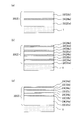
- 2 (a) to 2 (c) are schematic cross-sectional views of the strain gauge resistor.
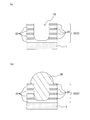
- FIG. 3 (a) is a schematic cross-sectional view of a lead wire connection portion in which a hole penetrating the etching stop layer is formed
- FIG. 3 (b) is a schematic view showing a state where the hole of the lead wire connection portion is filled
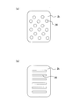
- FIGS. 4A and 4B are schematic top views of the lead wire connecting portion in which the hole is formed.
- FIG. 5 is a flowchart showing a method of manufacturing a strain gauge according to an embodiment of the present invention.
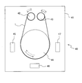
- FIG. 6 is a schematic view of a sputtering apparatus that can be used to form a laminate on a film-like substrate.
- the strain gauge 10 of the embodiment includes a base 1 and a resistor 2 provided on one surface of the base 1, and further includes a cover 3 covering the resistor 2. Good.
- the substrate 1 is a flexible plate-like member formed of a resin material, and more specifically, is a parallel flat plate.
- the resin material may be polyimide (PI), polyamide imide (PAI), polyethylene (PE), polyetheretherketone (PEEK) or the like.
- the thickness of the substrate 1 is, for example, about 12 ⁇ m to about 25 ⁇ m.
- the resistive element 2 has a pair of tabs (lead wire connection parts) 2t to which lead wires for external connection are joined, and a gauge sense that extends while being folded in a zigzag from one tab 2t and is connected to the other tab 2t Part (strain sensing part) 2c.
- the resistor 2 is formed of a laminate 20 in which metal layers 22 and etching stop layers 24 are alternately stacked in a direction perpendicular to the substrate 1.
- the etching stop layer 24 is a layer having a low etching rate by the etching process of the metal layer 22 described later. That is, the etching stop layer 24 is a layer for preventing the metal layer 22 located below the metal layer 22 to be etched from being etched when the metal layer 22 is etched away.
- the metal layer 22 may be formed of, for example, a copper-nickel alloy or the like.
- the etching stop layer 24 may be made of, for example, an insulator such as SiO 2 or SiN, a noble metal such as Au, Pt or Rh, Ta or Ir resistant to an acid, or the like.
- Au can have a high etching rate by selecting a specific etching process different from the etching process of the metal layer 22. Therefore, when a thin Au layer is used as the etching stop layer 24, Au in the etching process described later Removal of the etching stop layer 24 is facilitated.
- the resistor 2 having the plurality of metal layers and the etching stop layer 24 positioned therebetween, the resistance value of the resistor 2 can be stably adjusted in the etching process described later.
- the laminate 20 includes a first metal layer 22a formed on the substrate 1, a first etching stop layer 24a formed on the first metal layer 22a, and a first etching. It may have a second metal layer 22b formed on the stop layer 24a. Further, as shown in FIG. 2 (b), a second etching stop layer 24b formed on the second metal layer 22b may be provided, and further, metal layers 22c and 22d and etching stop layers 24c and 24d may be provided. It is also good. As shown in FIG. 2 (b), the etching stop layer 24 d may be disposed as the top layer of the laminate 20 (that is, the top layer of the resistor 2).
- the arrangement of the etching stop layer 24 d as the top layer of the laminate 20 has an advantage that the etching stop layer 24 d functions as a protective layer. Further, as shown in FIG. 2C, the etching stop layer 24 may be unevenly distributed in the vicinity of the surface of the laminate 20. That is, the thickness of the first metal layer 22a may be larger than the thicknesses of the metal layers 22b, 22c, and 22d other than the first metal layer 22a. In this case, the resistance value of the resistor 2 can be adjusted more finely than in the case where the same number of etching stop layers 24 are arranged at equal intervals in the stacked body 20 (see FIG. 2B).
- holes 26 penetrating the etching stop layer 24 may be formed.
- the etching stop layer 24 is an insulator, as shown in FIG. 3B, the holes 26 are filled with the conductor 28 so that the conductor 28 is interposed in the laminate 20 (ie, in the resistor 2).
- a plurality of metal layers 22 can be electrically connected.
- the plurality of metal layers 22 are electrically connected in the lead wire connection portion 2t, whereby the plurality of metal layers 22 in the strain sensing portion 2c are connected in parallel.
- the shape and arrangement of the holes 26 are not particularly limited.
- the hole 26 may have a circular planar shape as shown in FIG. 4 (a), or may have a linear planar shape as shown in FIG. 4 (b).
- the conductor 28 may be solder or the like.
- the cover 3 is provided on the resistor 2 so as to cover only the strain sensing portion 2 c of the resistor 2, and prevents the strain sensing portion 2 c from being damaged or the like.
- the cover 3 may be formed of polyimide as an example, but may be PAI, PE, PEEK or the like described above. In FIG. 1, the cover 3 is indicated by a broken line in order to clearly show the strain sensing part 2 c of the resistor 2.
- a sputtering apparatus 40 as schematically shown in FIG. 6 can be used.
- the sputtering apparatus 40 includes a vacuum chamber 41. Inside the vacuum chamber 41, a first roll 42 for unwinding or winding a flexible film-like (belt-like) substrate 1 and a second roll 43 for winding or unwinding the film-like substrate 1 are provided.
- a film forming roll 44 is installed between the transport paths which are installed and taken up by the second roll 43 and the substrate 1 drawn out from the first roll 42.
- a guide roll (not shown) for transporting the substrate 1 may be installed.
- the substrate 1 is wound around the film forming roll 44 and conveyed along the outer periphery of the film forming roll 44.
- the first target 45, the second target 46, and the third target 47 are disposed to face the substrate 1 wound around the film forming roll 44. That is, the first target 45, the second target 46, and the third target 47 are disposed to face the outer peripheral surface of the film forming roll 44.
- the first target 45 and the third target 47 are targets for forming the etching stop layer 24.
- the second target 46 is a target for forming the metal layer 22.
- the second target 26 is disposed between the first target 45 and the third target 47 in the transport direction of the substrate 1.
- the laminated body 20 can be formed into a film as follows using the sputtering device 40. First, the inside of the vacuum chamber 41 is depressurized to a high vacuum. Next, a rare gas such as Ar is introduced into the vacuum chamber 41, and atoms of the second target 46 and the third target 47 are knocked out by DC plasma or high frequency plasma, while the substrate 1 is shown by the solid arrow in FIG. Transport in the (first transport direction). That is, the base material 1 is fed from the first roll 42 toward the film forming roll 44 and conveyed along the film forming roll 44 while being in contact with the surface thereof, and conveyed from the film forming roll 44 toward the second roll 43 Then, take up by the second roll 43.
- a rare gas such as Ar
- the base material 1 passes a position facing the second target 46, atoms ejected from the second target 46 are deposited on the surface of the base material 1 to form the first metal layer 22a.
- the base material 1 passes a position facing the third target 47, the atoms knocked out of the third target 47 are deposited on the first metal layer 22a, whereby the first metal layer 22a is formed on the first metal layer 22a.
- An etching stop layer 24a is formed.
- the base material 1 passes a position facing the second target 46, atoms ejected from the second target 46 are deposited on the first etching stop layer 24a on the base material 1, and the second metal layer 22b is deposited. Is formed.
- the base material 1 passes a position facing the first target 45 atoms ejected from the first target 45 are deposited on the second metal layer 22b, and the second etching stop layer 24b is formed.
- the sputter deposition using the second target 46 and the third target 47 and the first target 45 and the second target 46 are used while reciprocating the base material 1 between the first roll 42 and the second roll 43.
- the metal layer 22 and the etching stop layer 24 can be alternately formed, and the laminate 20 can be formed.
- the substrate 1 is used as the targets 45, 46, 47.
- the opposing time can be shortened. Therefore, when the base material 1 passes the position which opposes the targets 45, 46, and 47, it can suppress that the base material 1 is heated and damaged.
- the film-forming roll 44 may be provided with a cooling mechanism (not shown), and the base material 1 may be cooled.
- the stacked body 20 may be formed by an electron beam heating evaporation method, a resistance heating evaporation method, or the like.
- the laminate 20 is patterned using photolithography to form a resistor 2 (see FIG. 1).
- a resist pattern can be formed on the laminate 20 by photolithography and the laminate 20 can be etched to form the resistor 2.
- the resistor 2 can be formed by forming a resist pattern on the substrate 1 and forming the laminate 20 thereon and then removing the resist and the laminate 20 on the resist.
- the resistance value of the resistor 2 may vary depending on the patterning accuracy in the resistor formation step, the resistance value of the resistor 2 is smaller than the design value (target value), and the magnitude of the deviation is within the allowable range. If it exceeds, the resistance value of the resistor 2 can be adjusted by etching the metal layer 24. For example, after the etching stop layer 24 of the uppermost layer of the resistor 2 is removed, the metal layer 22 (the uppermost metal layer of the metal layers) is etched to form the uppermost metal layer of the resistor 2 22 can be removed.
- the etching stop layer 24 is removed by wet etching using an aqueous solution of NH 4 F: HF: H 2 O or an aqueous solution of H 3 PO 4 : HNO 3 , or using a fluorine-based gas (CHF 3 , C 2 F 6 ) Can be performed by dry etching.
- the etching process of the metal layer 22 can be performed by an etching method such as reactive ion etching using an appropriate gas, sputter etching, or the like in which the etching rate ratio (selection ratio) of the metal layer 22 to the etching stop layer 24 is sufficiently large. .
- the etching stop layer 24 is not or hardly etched by the etching process of the metal layer 22, it is possible to etch substantially only the metal layer 22 of the uppermost layer of the resistor 2. By removing one metal layer 22 as described above, the resistance value of the resistor 2 can be increased. Furthermore, when it is necessary to increase the resistance value of the resistor 2, the etching stop layer 24 may be removed and the metal layer 22 may be etched again. By repeating this, the resistance value of the resistor 2 can be adjusted stepwise. When the difference between the resistance value of the resistor 2 measured in the above-described resistance value measurement process and the design value is within the allowable range, it is not necessary to perform the etching process.
- a hole 26 is formed in the lead wire connection portion 2t of the resistor 2.
- the holes 26 can be formed by a method of laser blasting the lead wire connection portion 2t, a method of pressing a jig connected to an ultrasonic oscillator against the lead wire connection portion 2t, or the like.
- the strain sensing unit 2 c may be covered with a cover 3 such as polyimide.
- the hole 26 is filled with a conductor 28 (see FIG. 3B) to form a conductor 20 in the resistor 2 (ie, the laminate 20). Electrically connect the plurality of metal layers 22).
- a strain gauge of the present invention since the resistance value of the strain gauge resistor can be easily and accurately adjusted, a strain gauge having a resistor of a desired resistance value can be manufactured with high yield. Therefore, it is possible to contribute to high accuracy and low price of the strain gauge and the measuring instrument using the same.
- 1 substrate, 2 resistors, 3 covers, 10 strain gauges, 20 laminates, 22 metal layers, 24 etching stop layers
Landscapes
- Physics & Mathematics (AREA)
- General Physics & Mathematics (AREA)
- Engineering & Computer Science (AREA)
- Mechanical Engineering (AREA)
- Measurement Of Length, Angles, Or The Like Using Electric Or Magnetic Means (AREA)
- Laminated Bodies (AREA)
- Physical Vapour Deposition (AREA)
Abstract
所望の抵抗値の抵抗体を有するひずみゲージを歩留まりよく製造することができる製造方法を提供する。ひずみゲージの製造方法は、基材上に金属層22とエッチングストップ層24を交互に形成することにより積層体20を形成することと、前記積層体20をパターニングして抵抗体を形成することを含む。抵抗体の抵抗値に応じて最上側の金属層22b(22d)をエッチング除去してもよい。
Description
本発明は、ひずみゲージ及びひずみゲージの製造方法に関する。
ひずみゲージは一般に、絶縁性を有する板状の基材と、基材の一面上に設けられた抵抗体とを有し、基材の他面が起歪体の表面に接着剤によって固定されている。起歪体は一般にアルミニウム合金等の金属製であり、計測対象の重量に応じて変形する(ひずみを生じる)。起歪体に変形(ひずみ)が生じるとこれに応じてひずみゲージの抵抗体に伸縮が生じ、抵抗体の電気抵抗値が変化する。この抵抗体の電気抵抗値の変化に基づいてひずみ量が求められる。ひずみセンサの一例は特許文献1に開示されている。
ひずみゲージの抵抗体は金属膜をパターニングすることによって形成されるが、パターニングの精度が低い場合、抵抗体の寸法のばらつきにより抵抗体の抵抗値がばらつくことがある。しかし、ひずみゲージの量産においては、所望の抵抗値の抵抗体を歩留まりよく形成することが望まれる。
そこで、本発明は、所望の抵抗値の抵抗体を有するひずみゲージを歩留まりよく製造することができる製造方法を提供することを目的とする。
本発明の第1の態様に従えば、基材上に金属層とエッチングストップ層を交互に形成することにより積層体を形成することと、
前記積層体をパターニングして抵抗体を形成することを含むひずみゲージの製造方法が提供される。
前記積層体をパターニングして抵抗体を形成することを含むひずみゲージの製造方法が提供される。
第1の態様のひずみゲージの製造方法において、前記積層体を形成することが、前記基材上に第1金属層を形成し、前記第1金属層上に第1エッチングストップ層を形成し、前記第1エッチングストップ層上に第2金属層を形成することを含んでよい。前記積層体を形成することは、前記第2金属層上に第2エッチングストップ層を形成することをさらに含んでよい。
第1の態様のひずみゲージの製造方法は、前記抵抗体を形成した後に、前記金属層のうちの少なくとも最上側の前記金属層をエッチングすることをさらに含んでよい。前記形成した抵抗体の抵抗値を測定することをさらに含み、前記測定された抵抗値に応じて、前記金属層のうちの少なくとも最上側の金属層をエッチングしてもよい。
第1の態様のひずみゲージの製造方法において、前記エッチングストップ層は絶縁体から形成されてよい。
第1の態様のひずみゲージの製造方法において、前記抵抗体が、一対のリード線接続部と、前記リード線接続部の一方からジグザグに折り返しながら延在して前記リード線接続部の他方に接続するひずみ受感部とを有してよく、
第1の態様のひずみゲージの製造方法が、前記一対のリード線接続部に前記エッチングストップ層を貫通する孔を形成することをさらに含んでよい。前記孔に導電体を充填して、前記積層体の前記金属層同士を電気的に接続することをさらに含んでもよい。
第1の態様のひずみゲージの製造方法が、前記一対のリード線接続部に前記エッチングストップ層を貫通する孔を形成することをさらに含んでよい。前記孔に導電体を充填して、前記積層体の前記金属層同士を電気的に接続することをさらに含んでもよい。
第1の態様のひずみゲージの製造方法において、前記エッチングストップ層が前記積層体の最上層として配置されてよい。
第1の態様のひずみゲージの製造方法において、前記基材がフィルム状の基材であり、
前記基材を前記金属層の材料からなるスパッタリングターゲットに対向する位置と前記エッチングストップ層の材料からなるスパッタリングターゲットに対向する位置の間を往復搬送しながらスパッタリングを行うことにより、前記積層体を形成してよい。前記金属層の材料からなるスパッタリングターゲット及び前記エッチングストップ層の材料からなるスパッタリングターゲットを成膜ロールの外周面に対向するように配置し、前記基材を前記成膜ロールの外周に沿って往復搬送しながら前記スパッタリングを行ってよい。
前記基材を前記金属層の材料からなるスパッタリングターゲットに対向する位置と前記エッチングストップ層の材料からなるスパッタリングターゲットに対向する位置の間を往復搬送しながらスパッタリングを行うことにより、前記積層体を形成してよい。前記金属層の材料からなるスパッタリングターゲット及び前記エッチングストップ層の材料からなるスパッタリングターゲットを成膜ロールの外周面に対向するように配置し、前記基材を前記成膜ロールの外周に沿って往復搬送しながら前記スパッタリングを行ってよい。
本発明の第2の態様に従えば、基材と、
前記基材上に設けられた抵抗体を備え、
前記抵抗体が、金属層とエッチングストップ層が交互に形成された積層体からなるひずみゲージが提供される。
前記基材上に設けられた抵抗体を備え、
前記抵抗体が、金属層とエッチングストップ層が交互に形成された積層体からなるひずみゲージが提供される。
第2の態様のひずみゲージにおいて、前記積層体が、前記基材上に形成された第1金属層と、前記第1金属層上に形成された第1エッチングストップ層と、前記第1エッチングストップ層上に形成された第2金属層を含んでよい。前記積層体は、前記第2金属層上に形成された第2エッチングストップ層をさらに含んでよい。
第2の態様のひずみゲージにおいて、前記エッチングストップ層が絶縁体から形成されてよい。また、前記第1金属層と前記第2金属層の厚みが異なっていてもよい。
第2の態様のひずみゲージにおいて、前記抵抗体が、一対のリード線接続部と、前記リード線接続部の一方からジグザグに折り返しながら延在して前記リード線接続部の他方に接続するひずみ受感部とを有し、
前記一対のリード線接続部において、前記エッチングストップ層を貫通する孔が形成されていてよい。前記積層体の前記金属層同士が、前記孔に充填された導電体により電気的に接続されていてよい。
前記一対のリード線接続部において、前記エッチングストップ層を貫通する孔が形成されていてよい。前記積層体の前記金属層同士が、前記孔に充填された導電体により電気的に接続されていてよい。
第2の態様のひずみゲージにおいて、前記エッチングストップ層が前記積層体の最上層として配置されてよい。
本発明のひずみゲージの製造方法では、金属層とエッチングストップ層を交互に積層した積層体から抵抗体を形成することにより、抵抗体の抵抗値を容易にかつ精度よく調整できる。そのため所望の抵抗値の抵抗体を有するひずみゲージを歩留りよく製造できる。
本発明のひずみゲージ及びその製造方法の実施形態について、図面を参照して説明する。
[ひずみゲージ]
図1に示す通り、実施形態のひずみゲージ10は、基材1と、基材1の一面上に設けられた抵抗体2とを有し、さらに、抵抗体2を覆うカバー3を有してよい。
図1に示す通り、実施形態のひずみゲージ10は、基材1と、基材1の一面上に設けられた抵抗体2とを有し、さらに、抵抗体2を覆うカバー3を有してよい。
基材1は、樹脂材料で形成された可撓性を有する板状部材であり、より具体的には平行平板である。樹脂材料は、ポリイミド(PI)、ポリアミドイミド(PAI)、ポリエチレン(PE)、ポリエーテルエーテルケトン(PEEK)などであってよい。基材1の厚さは例えば約12μm~約25μmmである。
抵抗体2は、外部接続用のリード線が接合される一対のタブ(リード線接続部)2tと、一方のタブ2tからジグザグに折り返しながら延在して他方のタブ2tに接続するゲージ受感部(ひずみ受感部)2cとを有する。
図2(a)~(c)に抵抗体2の断面構造を示す。抵抗体2は、基材1に対して垂直な方向に金属層22とエッチングストップ層24が交互に積層された積層体20からなる。エッチングストップ層24は、後述する金属層22のエッチング処理によるエッチングレートが低い層である。すなわち、エッチングストップ層24は、金属層22のエッチング除去において、エッチングされる金属層22より下側に位置する金属層22までがエッチングされることを防止するための層である。金属層22は、例えば銅ニッケル合金等から形成されてよい。エッチングストップ層24は、例えばSiO2やSiN等の絶縁体、Au、Pt、Rhなどの貴金属、酸に強いTaやIr等から形成されてよい。特にAuは、金属層22のエッチング処理とは異なる特定のエッチング処理を選択することで高いエッチングレートを有することができるため、エッチングストップ層24として薄いAu層を用いた場合、後述するエッチング工程におけるエッチングストップ層24の除去が容易になる。抵抗体2が複数の金属層とその間に位置するエッチングストップ層24を有することにより、後述するエッチング工程において抵抗体2の抵抗値の調整を安定的に行うことができる。
積層体20は、図2(a)に示すように、基材1上に形成された第1金属層22a、第1金属層22a上に形成された第1エッチングストップ層24aと、第1エッチングストップ層24a上に形成された第2金属層22bを有してよい。また、図2(b)に示すように、第2金属層22b上に形成された第2エッチングストップ層24bを備えてよく、さらに金属層22c、22dとエッチングストップ層24c、24dを有してもよい。図2(b)に示すように、エッチングストップ層24dが積層体20の最上層(すなわち、抵抗体2の最上層)として配置されていてもよい。積層体20の最上層としてエッチングストップ層24dが配置されることにより、当該エッチングストップ層24dが保護層として働くという利点がある。また、図2(c)に示すように、積層体20の表面付近にエッチングストップ層24が偏在していてもよい。すなわち、第1金属層22aの厚みが、第1金属層22a以外の金属層22b、22c、22dの厚みよりも大きくてよい。この場合、同数のエッチングストップ層24が積層体20において均等な間隔で配置されている場合(図2(b)参照)と比べて、抵抗体2の抵抗値をより細かく調整できる。
前記一対のリード線接続部2tにおいて、図3(a)に示すようにエッチングストップ層24を貫通する孔26が形成されていてよい。エッチングストップ層24が絶縁体である場合、図3(b)に示すように孔26に導電体28を充填することにより、導電体28を介して積層体20中の(すなわち抵抗体2中の)複数の金属層22を電気的に接続することができる。リード線接続部2tにおいて複数の金属層22が電気的に接続されることにより、ひずみ受感部2cにおける複数の金属層22は並列に接続される。孔26の形状及び配置は特に限定されない。例えば、孔26が図4(a)に示す様に円形の平面形状を有してもよく、図4(b)に示す様に線状の平面形状を有してもよい。導電体28ははんだ等であってよい。
カバー3は、抵抗体2のひずみ受感部2cのみを覆うように抵抗体2の上に設けられ、ひずみ受感部2cに損傷等が生じることを防いでいる。カバー3は一例としてポリイミドで形成することができるが、前述のPAI、PE、PEEK等でもよい。なお、図1においては、抵抗体2のひずみ受感部2cを明示するためカバー3は破線で示している。
[ひずみゲージの製造方法]
次に、ひずみゲージ10の製造方法を、図5のフローチャートに従って説明する。
次に、ひずみゲージ10の製造方法を、図5のフローチャートに従って説明する。
図5に示す通り、ひずみゲージ10の製造方法は、基材上に、複数の金属層と少なくとも1つのエッチングストップ層を交互に形成することにより積層体を形成する工程(S01)と、積層体をパターニングして抵抗体を形成する工程(S02)と、抵抗体の抵抗値を測定する工程(S03)と、少なくとも1つの金属層をエッチングする工程(S04)と、一対のリード線接続部にエッチングストップ層を貫通する孔を形成する工程(S05)と、抵抗体2をカバー3で覆うカバー形成工程(S06)と、複数の金属層を電気的に接続する工程(S07)とを有する。S03~S07は任意の工程である。
<積層体形成工程>
積層体形成工程S01では、基材1上に金属層22とエッチングストップ層24を交互に形成する(図2(a)~(c)参照)。例えば、図6に概念的に示すようなスパッタリング装置40を用いることができる。スパッタリング装置40は、真空チャンバー41を備えている。真空チャンバー41の内部には、可撓性のあるフィルム状(ベルト状)の基材1を繰り出し又は巻き取る第1ロール42と、フィルム状の基材1を巻き取り又は繰り出す第2ロール43が設置され、第1ロール42から繰り出された基材1が第2ロール43により巻き取られるまでの搬送路の間に成膜ロール44が設置されている。さらに、真空チャンバー41内には基材1を搬送するためのガイドロール(不図示)が設置されていてもよい。基材1は、成膜ロール44に巻回され、成膜ロール44の外周に沿って搬送される。成膜ロール44に巻回される基材1に対向するように、第1ターゲット45、第2ターゲット46、第3ターゲット47が配置されている。すなわち、第1ターゲット45、第2ターゲット46、第3ターゲット47は、成膜ロール44の外周面に対向するように配置される。第1ターゲット45及び第3ターゲット47は、エッチングストップ層24を形成するためのターゲットである。第2ターゲット46は金属層22を形成するためのターゲットである。第2ターゲット26は、基材1の搬送方向において第1ターゲット45と第3ターゲット47の間に配置される。
積層体形成工程S01では、基材1上に金属層22とエッチングストップ層24を交互に形成する(図2(a)~(c)参照)。例えば、図6に概念的に示すようなスパッタリング装置40を用いることができる。スパッタリング装置40は、真空チャンバー41を備えている。真空チャンバー41の内部には、可撓性のあるフィルム状(ベルト状)の基材1を繰り出し又は巻き取る第1ロール42と、フィルム状の基材1を巻き取り又は繰り出す第2ロール43が設置され、第1ロール42から繰り出された基材1が第2ロール43により巻き取られるまでの搬送路の間に成膜ロール44が設置されている。さらに、真空チャンバー41内には基材1を搬送するためのガイドロール(不図示)が設置されていてもよい。基材1は、成膜ロール44に巻回され、成膜ロール44の外周に沿って搬送される。成膜ロール44に巻回される基材1に対向するように、第1ターゲット45、第2ターゲット46、第3ターゲット47が配置されている。すなわち、第1ターゲット45、第2ターゲット46、第3ターゲット47は、成膜ロール44の外周面に対向するように配置される。第1ターゲット45及び第3ターゲット47は、エッチングストップ層24を形成するためのターゲットである。第2ターゲット46は金属層22を形成するためのターゲットである。第2ターゲット26は、基材1の搬送方向において第1ターゲット45と第3ターゲット47の間に配置される。
スパッタリング装置40を用いて、以下のようにして積層体20を成膜することができる。まず、真空チャンバー41内を高真空に減圧する。次いで、真空チャンバー41内にAr等の希ガスを導入し、DCプラズマや高周波プラズマによって第2ターゲット46及び第3ターゲット47の原子を叩き出しながら、基材1を図6において実線矢印で示す方向(第1搬送方向)に搬送する。すなわち、基材1を、第1ロール42から成膜ロール44に向かって繰り出し、成膜ロール44に沿ってその表面に接触させながら搬送し、成膜ロール44から第2ロール43に向かって搬送して第2ロール43で巻き取る。基材1が第2ターゲット46に対向する位置を通過するときに、基材1の表面に第2ターゲット46から叩き出された原子が堆積されることにより第1金属層22aが形成される。基材1が第3ターゲット47に対向する位置を通過するときに、第1金属層22a上に第3ターゲット47から叩き出された原子が堆積されることにより第1金属層22a上に第1エッチングストップ層24aが形成される。
次いで、DCプラズマや高周波プラズマによって第1ターゲット45及び第2ターゲット46の原子を叩き出しながら、第2ロール43で巻き取った基材1を図6において破線矢印で示す方向(第2搬送方向)に搬送する。すなわち、基材1を、第2ロール43から成膜ロール44に向かって繰り出し、成膜ロール44に沿ってその表面に接触させながら搬送し、次いで成膜ロール44から第1ロール42に向かって搬送して第1ロール42で巻き取る。基材1が第2ターゲット46に対向する位置を通過するときに、基材1上の第1エッチングストップ層24a上に第2ターゲット46から叩き出された原子が堆積され、第2金属層22bが形成される。基材1が第1ターゲット45に対向する位置を通過するときに、第2金属層22b上に第1ターゲット45から叩き出された原子が堆積され、第2エッチングストップ層24bが形成される。
基材1を第1ロール42と第2ロール43の間で往復搬送しながら、上記の第2ターゲット46及び第3ターゲット47を用いたスパッタ成膜と第1ターゲット45及び第2ターゲット46を用いたスパッタ成膜を繰り返すことにより、金属層22とエッチングストップ層24を交互に形成し、積層体20を形成することができる。
この積層体20の形成方法においては、積層体20全体の厚さに対して各金属層22及び各エッチングストップ層24の厚さが小さくてよいため、基材1がターゲット45、46、47に対向する時間を短くすることができる。そのため、基材1がターゲット45、46、47に対向する位置を通過する時に基材1が加熱されてダメージを受けることを抑制することができる。また、基材1への熱ダメージをさらに軽減するために、成膜ロール44に冷却機構(不図示)を設け、基材1を冷却してもよい。
スパッタ法に代えて、電子線加熱蒸着法、抵抗加熱蒸着法等により積層体20を形成してもよい。
<抵抗体形成工程>
次いで、フォトリソグラフィを用いて、積層体20をパターニングし、抵抗体2(図1参照)を形成する。具体的には積層体20上にフォトリソグラフィによりレジストパターンを形成し、積層体20をエッチングすることで抵抗体2を形成することができる。あるいは、基材1上にレジストパターンを形成し、その上に積層体20を形成した後レジスト及びレジスト上の積層体20を除去することによって抵抗体2を形成することもできる。
次いで、フォトリソグラフィを用いて、積層体20をパターニングし、抵抗体2(図1参照)を形成する。具体的には積層体20上にフォトリソグラフィによりレジストパターンを形成し、積層体20をエッチングすることで抵抗体2を形成することができる。あるいは、基材1上にレジストパターンを形成し、その上に積層体20を形成した後レジスト及びレジスト上の積層体20を除去することによって抵抗体2を形成することもできる。
<抵抗値測定工程>
形成した抵抗体2の一対のリード線接続部2tの間の抵抗値を測定する。
形成した抵抗体2の一対のリード線接続部2tの間の抵抗値を測定する。
<エッチング工程>
抵抗体形成工程のパターニング精度によっては抵抗体2の抵抗値にばらつきが生じることがあるが、抵抗体2の抵抗値が設計値(目標値)よりも小さく、そのずれの大きさが許容範囲を超えた場合、金属層24をエッチングすることにより抵抗体2の抵抗値を調整することができる。例えば、抵抗体2の最上層のエッチングストップ層24を除去した後、金属層22(金属層のうちの最上側の金属層)のエッチング処理を行うことで、抵抗体2の最上層の金属層22を除去することができる。エッチングストップ層24の除去は、NH4F:HF:H2Oの水溶液若しくはH3PO4:HNO3の水溶液を用いたウェットエッチング、又はフッ素系ガス(CHF3,C2F6)を用いたドライエッチングにより行うことができる。金属層22のエッチング処理は、適切なガスを用いた反応性イオンエッチング、スパッタエッチング等、金属層22とエッチングストップ層24のエッチングレートの比(選択比)が十分大きいエッチング法により行うことができる。エッチングストップ層24は金属層22のエッチング処理によってはエッチングされないまたはほとんどエッチングされないため、ほぼ抵抗体2の最上層の金属層22のみをエッチングすることができる。このように金属層22を1層除去することで、抵抗体2の抵抗値を上昇させることができる。さらに抵抗体2の抵抗値を上昇させる必要がある場合には、再度エッチングストップ層24の除去及び金属層22のエッチングを行ってよい。これを繰り返すことにより、抵抗体2の抵抗値を段階的に調整することができる。なお、上述の抵抗値測定工程で測定した抵抗体2の抵抗値と設計値とのずれが許容範囲内であった場合は、エッチング工程を行う必要はない。
抵抗体形成工程のパターニング精度によっては抵抗体2の抵抗値にばらつきが生じることがあるが、抵抗体2の抵抗値が設計値(目標値)よりも小さく、そのずれの大きさが許容範囲を超えた場合、金属層24をエッチングすることにより抵抗体2の抵抗値を調整することができる。例えば、抵抗体2の最上層のエッチングストップ層24を除去した後、金属層22(金属層のうちの最上側の金属層)のエッチング処理を行うことで、抵抗体2の最上層の金属層22を除去することができる。エッチングストップ層24の除去は、NH4F:HF:H2Oの水溶液若しくはH3PO4:HNO3の水溶液を用いたウェットエッチング、又はフッ素系ガス(CHF3,C2F6)を用いたドライエッチングにより行うことができる。金属層22のエッチング処理は、適切なガスを用いた反応性イオンエッチング、スパッタエッチング等、金属層22とエッチングストップ層24のエッチングレートの比(選択比)が十分大きいエッチング法により行うことができる。エッチングストップ層24は金属層22のエッチング処理によってはエッチングされないまたはほとんどエッチングされないため、ほぼ抵抗体2の最上層の金属層22のみをエッチングすることができる。このように金属層22を1層除去することで、抵抗体2の抵抗値を上昇させることができる。さらに抵抗体2の抵抗値を上昇させる必要がある場合には、再度エッチングストップ層24の除去及び金属層22のエッチングを行ってよい。これを繰り返すことにより、抵抗体2の抵抗値を段階的に調整することができる。なお、上述の抵抗値測定工程で測定した抵抗体2の抵抗値と設計値とのずれが許容範囲内であった場合は、エッチング工程を行う必要はない。
<孔形成工程>
エッチングストップ層24が絶縁体である場合、抵抗体2のリード線接続部2tに孔26(図3(a)参照)を形成する。孔26は、リード線接続部2tをレーザブラスト加工する方法、超音波発振器と接続した治具をリード線接続部2tに押し当てる方法等により形成することができる。
エッチングストップ層24が絶縁体である場合、抵抗体2のリード線接続部2tに孔26(図3(a)参照)を形成する。孔26は、リード線接続部2tをレーザブラスト加工する方法、超音波発振器と接続した治具をリード線接続部2tに押し当てる方法等により形成することができる。
<カバー形成工程>
抵抗体2のひずみ受感部2cを保護するため、ポリイミド等のカバー3でひずみ受感部2cを覆ってよい。
抵抗体2のひずみ受感部2cを保護するため、ポリイミド等のカバー3でひずみ受感部2cを覆ってよい。
<金属層の電気的接続工程>
エッチングストップ層24が絶縁体である場合、孔26にはんだ等の導電体28(図3(b)参照)を充填することにより、導電体28を介して抵抗体2中の(すなわち積層体20中の)複数の金属層22を電気的に接続する。
エッチングストップ層24が絶縁体である場合、孔26にはんだ等の導電体28(図3(b)参照)を充填することにより、導電体28を介して抵抗体2中の(すなわち積層体20中の)複数の金属層22を電気的に接続する。
本発明の特徴を維持する限り、本発明は上記実施の形態に限定されるものではなく、本発明の技術的思想の範囲内で考えられるその他の形態についても、本発明の範囲内に含まれる。
本発明のひずみゲージの製造方法では、ひずみゲージの抵抗体の抵抗値を容易にかつ精度よく調整できるため、所望の抵抗値の抵抗体を有するひずみゲージを歩留りよく製造できる。したがって、ひずみゲージやこれを用いた計測機器の高精度化及び低価格化に貢献することができる。
1 基材、2 抵抗体、3 カバー、10 ひずみゲージ、20 積層体、22 金属層、24 エッチングストップ層
Claims (19)
- 基材上に金属層とエッチングストップ層を交互に形成することにより積層体を形成することと、
前記積層体をパターニングして抵抗体を形成することを含むひずみゲージの製造方法。 - 前記積層体を形成することが、前記基材上に第1金属層を形成し、前記第1金属層上に第1エッチングストップ層を形成し、前記第1エッチングストップ層上に第2金属層を形成することを含む請求項1に記載のひずみゲージの製造方法。
- 前記積層体を形成することが前記第2金属層上に第2エッチングストップ層を形成することを含む請求項2に記載のひずみゲージの製造方法。
- 前記抵抗体を形成した後に、前記金属層のうちの少なくとも最上側の金属層をエッチングすることを含む請求項1~3のいずれか一項に記載のひずみゲージの製造方法。
- 前記形成した抵抗体の抵抗値を測定することをさらに含み、前記測定された抵抗値に応じて、前記金属層のうちの少なくとも最上側の金属層をエッチングする請求項4に記載のひずみゲージの製造方法。
- 前記エッチングストップ層が絶縁体から形成される請求項1~5のいずれか一項に記載のひずみゲージの製造方法。
- 前記抵抗体が、一対のリード線接続部と、前記リード線接続部の一方からジグザグに折り返しながら延在して前記リード線接続部の他方に接続するひずみ受感部とを有し、
前記一対のリード線接続部に前記エッチングストップ層を貫通する孔を形成することを含む請求項6に記載のひずみゲージの製造方法。 - 前記孔に導電体を充填して、前記積層体の前記金属層同士を電気的に接続することを含む請求項7に記載のひずみゲージの製造方法。
- 前記エッチングストップ層が前記積層体の最上層として配置される請求項1~8のいずれか一項に記載のひずみゲージの製造方法。
- 前記基材がフィルム状の基材であり、
前記基材を前記金属層の材料からなるスパッタリングターゲットに対向する位置と前記エッチングストップ層の材料からなるスパッタリングターゲットに対向する位置の間を往復搬送しながらスパッタリングを行うことにより、前記積層体を形成する請求項1~9のいずれか一項に記載のひずみゲージの製造方法。 - 前記金属層の材料からなるスパッタリングターゲット及び前記エッチングストップ層の材料からなるスパッタリングターゲットを成膜ロールの外周面に対向するように配置し、前記基材を前記成膜ロールの外周に沿って往復搬送しながら前記スパッタリングを行う請求項10に記載のひずみゲージの製造方法。
- 基材と、
前記基材上に設けられた抵抗体を備え、
前記抵抗体が、金属層とエッチングストップ層が交互に形成された積層体からなるひずみゲージ。 - 前記積層体が、前記基材上に形成された第1金属層と、前記第1金属層上に形成された第1エッチングストップ層と、前記第1エッチングストップ層上に形成された第2金属層を含む請求項12に記載のひずみゲージ。
- 前記積層体が、前記第2金属層上に形成された第2エッチングストップ層を含む請求項13に記載のひずみゲージ。
- 前記第1金属層と前記第2金属層の厚みが異なる請求項12~14のいずれか一項に記載のひずみゲージ。
- 前記エッチングストップ層が絶縁体から形成される請求項12~15のいずれか一項に記載のひずみゲージ。
- 前記抵抗体が、一対のリード線接続部と、前記リード線接続部の一方からジグザグに折り返しながら延在して前記リード線接続部の他方に接続するひずみ受感部とを有し、
前記一対のリード線接続部において、前記エッチングストップ層を貫通する孔が形成されている請求項16に記載のひずみゲージ。 - 前記積層体の前記金属層同士が、前記孔に充填された導電体により電気的に接続されている請求項17に記載のひずみゲージ。
- 前記エッチングストップ層が前記積層体の最上層として配置されている請求項12~18のいずれか一項に記載のひずみゲージ。
Applications Claiming Priority (2)
| Application Number | Priority Date | Filing Date | Title |
|---|---|---|---|
| JP2017215327A JP6764848B2 (ja) | 2017-11-08 | 2017-11-08 | ひずみゲージ及びひずみゲージの製造方法 |
| JP2017-215327 | 2017-11-08 |
Publications (1)
| Publication Number | Publication Date |
|---|---|
| WO2019093373A1 true WO2019093373A1 (ja) | 2019-05-16 |
Family
ID=66437807
Family Applications (1)
| Application Number | Title | Priority Date | Filing Date |
|---|---|---|---|
| PCT/JP2018/041336 Ceased WO2019093373A1 (ja) | 2017-11-08 | 2018-11-07 | ひずみゲージ及びひずみゲージの製造方法 |
Country Status (2)
| Country | Link |
|---|---|
| JP (1) | JP6764848B2 (ja) |
| WO (1) | WO2019093373A1 (ja) |
Cited By (1)
| Publication number | Priority date | Publication date | Assignee | Title |
|---|---|---|---|---|
| US20230175831A1 (en) * | 2020-04-08 | 2023-06-08 | Minebea Mitsumi Inc. | Strain gauge |
Families Citing this family (2)
| Publication number | Priority date | Publication date | Assignee | Title |
|---|---|---|---|---|
| US11218728B2 (en) * | 2019-06-04 | 2022-01-04 | Tencent America LLC | Method and apparatus for video coding |
| JP7575162B2 (ja) * | 2021-06-04 | 2024-10-29 | ミネベアミツミ株式会社 | ひずみゲージ |
Citations (4)
| Publication number | Priority date | Publication date | Assignee | Title |
|---|---|---|---|---|
| JPH047826A (ja) * | 1990-04-25 | 1992-01-13 | Fuji Xerox Co Ltd | 半導体装置の製造方法 |
| JPH05257105A (ja) * | 1991-12-27 | 1993-10-08 | Fujitsu Ltd | 光導波路デバイス |
| JPH0936061A (ja) * | 1995-07-18 | 1997-02-07 | Fujitsu Ltd | 半導体装置の製造方法 |
| JP2006234384A (ja) * | 2005-02-22 | 2006-09-07 | Toshiba Hokuto Electronics Corp | 歪ゲージ装置 |
Family Cites Families (5)
| Publication number | Priority date | Publication date | Assignee | Title |
|---|---|---|---|---|
| US4176445A (en) * | 1977-06-03 | 1979-12-04 | Angstrohm Precision, Inc. | Metal foil resistor |
| DE3431114A1 (de) * | 1984-08-24 | 1986-03-06 | Vdo Adolf Schindling Ag, 6000 Frankfurt | Elektrischer widerstand |
| FR2693795B1 (fr) * | 1992-07-15 | 1994-08-19 | Commissariat Energie Atomique | Jauge de contrainte sur support souple et capteur muni de ladite jauge. |
| JP5319373B2 (ja) * | 2009-04-10 | 2013-10-16 | 富士フイルム株式会社 | ガスバリアフィルムおよびガスバリアフィルムの製造方法 |
| JP2016166378A (ja) * | 2013-07-11 | 2016-09-15 | 日産自動車株式会社 | 表面処理装置および表面処理方法 |
-
2017
- 2017-11-08 JP JP2017215327A patent/JP6764848B2/ja active Active
-
2018
- 2018-11-07 WO PCT/JP2018/041336 patent/WO2019093373A1/ja not_active Ceased
Patent Citations (4)
| Publication number | Priority date | Publication date | Assignee | Title |
|---|---|---|---|---|
| JPH047826A (ja) * | 1990-04-25 | 1992-01-13 | Fuji Xerox Co Ltd | 半導体装置の製造方法 |
| JPH05257105A (ja) * | 1991-12-27 | 1993-10-08 | Fujitsu Ltd | 光導波路デバイス |
| JPH0936061A (ja) * | 1995-07-18 | 1997-02-07 | Fujitsu Ltd | 半導体装置の製造方法 |
| JP2006234384A (ja) * | 2005-02-22 | 2006-09-07 | Toshiba Hokuto Electronics Corp | 歪ゲージ装置 |
Cited By (2)
| Publication number | Priority date | Publication date | Assignee | Title |
|---|---|---|---|---|
| US20230175831A1 (en) * | 2020-04-08 | 2023-06-08 | Minebea Mitsumi Inc. | Strain gauge |
| US12523461B2 (en) * | 2020-04-08 | 2026-01-13 | Minebea Mitsumi Inc. | Strain gauge |
Also Published As
| Publication number | Publication date |
|---|---|
| JP6764848B2 (ja) | 2020-10-07 |
| JP2019086420A (ja) | 2019-06-06 |
Similar Documents
| Publication | Publication Date | Title |
|---|---|---|
| JP6451654B2 (ja) | コイル部品 | |
| WO2019093373A1 (ja) | ひずみゲージ及びひずみゲージの製造方法 | |
| JP5783297B2 (ja) | 力学量センサ | |
| JP3678180B2 (ja) | フローセンサ | |
| JP5305735B2 (ja) | 微小電気機械システム装置およびその製造方法 | |
| JP5425801B2 (ja) | 電気抵抗膜付き金属箔及びその製造方法 | |
| TWI570825B (zh) | 利用黏合劑層疊金屬薄板的半導體檢測板及其製造方法 | |
| WO2022092205A1 (ja) | 積層フィルム、その製造方法およびひずみセンサ | |
| JP5040403B2 (ja) | 圧電薄膜振動装置及びその製造方法 | |
| WO2022092204A1 (ja) | 積層フィルムおよび歪みセンサ | |
| KR20130119986A (ko) | 공간 절약적 사용을 위한 탈착 가능한 마이크로 부품 및 나노 부품 | |
| KR20180072521A (ko) | 압력센서 및 그 제조방법 | |
| JP6281383B2 (ja) | 半導体素子 | |
| JP4293178B2 (ja) | 立体回路基板の製造方法 | |
| US11054326B2 (en) | Physical quantity sensor | |
| CN116438062A (zh) | 层叠薄膜、第2层叠薄膜的制造方法和应变传感器的制造方法 | |
| JP2005337956A (ja) | 物理量センサとその製法 | |
| JP5447693B2 (ja) | 加速度センサ | |
| TWI921402B (zh) | 積層膜、其製造方法及應變感測器 | |
| TWI843803B (zh) | 溫度感測膜、導電膜及其製造方法 | |
| JP2006147812A (ja) | 積層薄膜電気配線板 | |
| JP7435734B2 (ja) | 樹脂多層基板 | |
| CN104900358A (zh) | 薄膜电阻器制法 | |
| US12563677B2 (en) | Multilayer substrate and method of manufacturing multilayer substrate | |
| TW202231465A (zh) | 應變感測器及積層體 |
Legal Events
| Date | Code | Title | Description |
|---|---|---|---|
| 121 | Ep: the epo has been informed by wipo that ep was designated in this application |
Ref document number: 18877201 Country of ref document: EP Kind code of ref document: A1 |
|
| NENP | Non-entry into the national phase |
Ref country code: DE |
|
| 122 | Ep: pct application non-entry in european phase |
Ref document number: 18877201 Country of ref document: EP Kind code of ref document: A1 |