WO2019087470A1 - 表示装置 - Google Patents
表示装置 Download PDFInfo
- Publication number
- WO2019087470A1 WO2019087470A1 PCT/JP2018/026154 JP2018026154W WO2019087470A1 WO 2019087470 A1 WO2019087470 A1 WO 2019087470A1 JP 2018026154 W JP2018026154 W JP 2018026154W WO 2019087470 A1 WO2019087470 A1 WO 2019087470A1
- Authority
- WO
- WIPO (PCT)
- Prior art keywords
- insulating film
- display device
- inorganic insulating
- upper surfaces
- region
- Prior art date
- Legal status (The legal status is an assumption and is not a legal conclusion. Google has not performed a legal analysis and makes no representation as to the accuracy of the status listed.)
- Ceased
Links
Images








Classifications
-
- G—PHYSICS
- G06—COMPUTING OR CALCULATING; COUNTING
- G06F—ELECTRIC DIGITAL DATA PROCESSING
- G06F3/00—Input arrangements for transferring data to be processed into a form capable of being handled by the computer; Output arrangements for transferring data from processing unit to output unit, e.g. interface arrangements
- G06F3/01—Input arrangements or combined input and output arrangements for interaction between user and computer
- G06F3/03—Arrangements for converting the position or the displacement of a member into a coded form
- G06F3/041—Digitisers, e.g. for touch screens or touch pads, characterised by the transducing means
- G06F3/0412—Digitisers structurally integrated in a display
-
- G—PHYSICS
- G02—OPTICS
- G02F—OPTICAL DEVICES OR ARRANGEMENTS FOR THE CONTROL OF LIGHT BY MODIFICATION OF THE OPTICAL PROPERTIES OF THE MEDIA OF THE ELEMENTS INVOLVED THEREIN; NON-LINEAR OPTICS; FREQUENCY-CHANGING OF LIGHT; OPTICAL LOGIC ELEMENTS; OPTICAL ANALOGUE/DIGITAL CONVERTERS
- G02F1/00—Devices or arrangements for the control of the intensity, colour, phase, polarisation or direction of light arriving from an independent light source, e.g. switching, gating or modulating; Non-linear optics
- G02F1/01—Devices or arrangements for the control of the intensity, colour, phase, polarisation or direction of light arriving from an independent light source, e.g. switching, gating or modulating; Non-linear optics for the control of the intensity, phase, polarisation or colour
- G02F1/13—Devices or arrangements for the control of the intensity, colour, phase, polarisation or direction of light arriving from an independent light source, e.g. switching, gating or modulating; Non-linear optics for the control of the intensity, phase, polarisation or colour based on liquid crystals, e.g. single liquid crystal display cells
- G02F1/133—Constructional arrangements; Operation of liquid crystal cells; Circuit arrangements
- G02F1/1333—Constructional arrangements; Manufacturing methods
- G02F1/133305—Flexible substrates, e.g. plastics, organic film
-
- G—PHYSICS
- G02—OPTICS
- G02F—OPTICAL DEVICES OR ARRANGEMENTS FOR THE CONTROL OF LIGHT BY MODIFICATION OF THE OPTICAL PROPERTIES OF THE MEDIA OF THE ELEMENTS INVOLVED THEREIN; NON-LINEAR OPTICS; FREQUENCY-CHANGING OF LIGHT; OPTICAL LOGIC ELEMENTS; OPTICAL ANALOGUE/DIGITAL CONVERTERS
- G02F1/00—Devices or arrangements for the control of the intensity, colour, phase, polarisation or direction of light arriving from an independent light source, e.g. switching, gating or modulating; Non-linear optics
- G02F1/01—Devices or arrangements for the control of the intensity, colour, phase, polarisation or direction of light arriving from an independent light source, e.g. switching, gating or modulating; Non-linear optics for the control of the intensity, phase, polarisation or colour
- G02F1/13—Devices or arrangements for the control of the intensity, colour, phase, polarisation or direction of light arriving from an independent light source, e.g. switching, gating or modulating; Non-linear optics for the control of the intensity, phase, polarisation or colour based on liquid crystals, e.g. single liquid crystal display cells
- G02F1/133—Constructional arrangements; Operation of liquid crystal cells; Circuit arrangements
- G02F1/1333—Constructional arrangements; Manufacturing methods
- G02F1/1345—Conductors connecting electrodes to cell terminals
-
- G—PHYSICS
- G06—COMPUTING OR CALCULATING; COUNTING
- G06F—ELECTRIC DIGITAL DATA PROCESSING
- G06F1/00—Details not covered by groups G06F3/00 - G06F13/00 and G06F21/00
- G06F1/16—Constructional details or arrangements
- G06F1/1613—Constructional details or arrangements for portable computers
- G06F1/1626—Constructional details or arrangements for portable computers with a single-body enclosure integrating a flat display, e.g. Personal Digital Assistants [PDAs]
-
- G—PHYSICS
- G06—COMPUTING OR CALCULATING; COUNTING
- G06F—ELECTRIC DIGITAL DATA PROCESSING
- G06F1/00—Details not covered by groups G06F3/00 - G06F13/00 and G06F21/00
- G06F1/16—Constructional details or arrangements
- G06F1/1613—Constructional details or arrangements for portable computers
- G06F1/1633—Constructional details or arrangements of portable computers not specific to the type of enclosures covered by groups G06F1/1615 - G06F1/1626
- G06F1/1637—Details related to the display arrangement, including those related to the mounting of the display in the housing
-
- G—PHYSICS
- G06—COMPUTING OR CALCULATING; COUNTING
- G06F—ELECTRIC DIGITAL DATA PROCESSING
- G06F1/00—Details not covered by groups G06F3/00 - G06F13/00 and G06F21/00
- G06F1/16—Constructional details or arrangements
- G06F1/1613—Constructional details or arrangements for portable computers
- G06F1/1633—Constructional details or arrangements of portable computers not specific to the type of enclosures covered by groups G06F1/1615 - G06F1/1626
- G06F1/1637—Details related to the display arrangement, including those related to the mounting of the display in the housing
- G06F1/1652—Details related to the display arrangement, including those related to the mounting of the display in the housing the display being flexible, e.g. mimicking a sheet of paper, or rollable
-
- G—PHYSICS
- G06—COMPUTING OR CALCULATING; COUNTING
- G06F—ELECTRIC DIGITAL DATA PROCESSING
- G06F1/00—Details not covered by groups G06F3/00 - G06F13/00 and G06F21/00
- G06F1/16—Constructional details or arrangements
- G06F1/18—Packaging or power distribution
- G06F1/189—Power distribution
-
- G—PHYSICS
- G09—EDUCATION; CRYPTOGRAPHY; DISPLAY; ADVERTISING; SEALS
- G09F—DISPLAYING; ADVERTISING; SIGNS; LABELS OR NAME-PLATES; SEALS
- G09F9/00—Indicating arrangements for variable information in which the information is built-up on a support by selection or combination of individual elements
- G09F9/30—Indicating arrangements for variable information in which the information is built-up on a support by selection or combination of individual elements in which the desired character or characters are formed by combining individual elements
- G09F9/301—Indicating arrangements for variable information in which the information is built-up on a support by selection or combination of individual elements in which the desired character or characters are formed by combining individual elements flexible foldable or roll-able electronic displays, e.g. thin LCD, OLED
-
- H—ELECTRICITY
- H05—ELECTRIC TECHNIQUES NOT OTHERWISE PROVIDED FOR
- H05B—ELECTRIC HEATING; ELECTRIC LIGHT SOURCES NOT OTHERWISE PROVIDED FOR; CIRCUIT ARRANGEMENTS FOR ELECTRIC LIGHT SOURCES, IN GENERAL
- H05B33/00—Electroluminescent light sources
- H05B33/02—Details
-
- H—ELECTRICITY
- H05—ELECTRIC TECHNIQUES NOT OTHERWISE PROVIDED FOR
- H05B—ELECTRIC HEATING; ELECTRIC LIGHT SOURCES NOT OTHERWISE PROVIDED FOR; CIRCUIT ARRANGEMENTS FOR ELECTRIC LIGHT SOURCES, IN GENERAL
- H05B33/00—Electroluminescent light sources
- H05B33/02—Details
- H05B33/06—Electrode terminals
-
- H—ELECTRICITY
- H05—ELECTRIC TECHNIQUES NOT OTHERWISE PROVIDED FOR
- H05B—ELECTRIC HEATING; ELECTRIC LIGHT SOURCES NOT OTHERWISE PROVIDED FOR; CIRCUIT ARRANGEMENTS FOR ELECTRIC LIGHT SOURCES, IN GENERAL
- H05B33/00—Electroluminescent light sources
- H05B33/12—Light sources with substantially two-dimensional [2D] radiating surfaces
- H05B33/22—Light sources with substantially two-dimensional [2D] radiating surfaces characterised by the chemical or physical composition or the arrangement of auxiliary dielectric or reflective layers
-
- H—ELECTRICITY
- H10—SEMICONDUCTOR DEVICES; ELECTRIC SOLID-STATE DEVICES NOT OTHERWISE PROVIDED FOR
- H10K—ORGANIC ELECTRIC SOLID-STATE DEVICES
- H10K59/00—Integrated devices, or assemblies of multiple devices, comprising at least one organic light-emitting element covered by group H10K50/00
- H10K59/10—OLED displays
- H10K59/12—Active-matrix OLED [AMOLED] displays
- H10K59/122—Pixel-defining structures or layers, e.g. banks
-
- H—ELECTRICITY
- H10—SEMICONDUCTOR DEVICES; ELECTRIC SOLID-STATE DEVICES NOT OTHERWISE PROVIDED FOR
- H10K—ORGANIC ELECTRIC SOLID-STATE DEVICES
- H10K59/00—Integrated devices, or assemblies of multiple devices, comprising at least one organic light-emitting element covered by group H10K50/00
- H10K59/10—OLED displays
- H10K59/12—Active-matrix OLED [AMOLED] displays
- H10K59/123—Connection of the pixel electrodes to the thin film transistors [TFT]
-
- H—ELECTRICITY
- H10—SEMICONDUCTOR DEVICES; ELECTRIC SOLID-STATE DEVICES NOT OTHERWISE PROVIDED FOR
- H10K—ORGANIC ELECTRIC SOLID-STATE DEVICES
- H10K59/00—Integrated devices, or assemblies of multiple devices, comprising at least one organic light-emitting element covered by group H10K50/00
- H10K59/10—OLED displays
- H10K59/12—Active-matrix OLED [AMOLED] displays
- H10K59/131—Interconnections, e.g. wiring lines or terminals
-
- H—ELECTRICITY
- H10—SEMICONDUCTOR DEVICES; ELECTRIC SOLID-STATE DEVICES NOT OTHERWISE PROVIDED FOR
- H10K—ORGANIC ELECTRIC SOLID-STATE DEVICES
- H10K77/00—Constructional details of devices covered by this subclass and not covered by groups H10K10/80, H10K30/80, H10K50/80 or H10K59/80
- H10K77/10—Substrates, e.g. flexible substrates
- H10K77/111—Flexible substrates
-
- G—PHYSICS
- G06—COMPUTING OR CALCULATING; COUNTING
- G06F—ELECTRIC DIGITAL DATA PROCESSING
- G06F2203/00—Indexing scheme relating to G06F3/00 - G06F3/048
- G06F2203/041—Indexing scheme relating to G06F3/041 - G06F3/045
- G06F2203/04102—Flexible digitiser, i.e. constructional details for allowing the whole digitising part of a device to be flexed or rolled like a sheet of paper
-
- G—PHYSICS
- G06—COMPUTING OR CALCULATING; COUNTING
- G06F—ELECTRIC DIGITAL DATA PROCESSING
- G06F2203/00—Indexing scheme relating to G06F3/00 - G06F3/048
- G06F2203/041—Indexing scheme relating to G06F3/041 - G06F3/045
- G06F2203/04111—Cross over in capacitive digitiser, i.e. details of structures for connecting electrodes of the sensing pattern where the connections cross each other, e.g. bridge structures comprising an insulating layer, or vias through substrate
-
- G—PHYSICS
- G06—COMPUTING OR CALCULATING; COUNTING
- G06F—ELECTRIC DIGITAL DATA PROCESSING
- G06F2203/00—Indexing scheme relating to G06F3/00 - G06F3/048
- G06F2203/041—Indexing scheme relating to G06F3/041 - G06F3/045
- G06F2203/04112—Electrode mesh in capacitive digitiser: electrode for touch sensing is formed of a mesh of very fine, normally metallic, interconnected lines that are almost invisible to see. This provides a quite large but transparent electrode surface, without need for ITO or similar transparent conductive material
-
- G—PHYSICS
- G06—COMPUTING OR CALCULATING; COUNTING
- G06F—ELECTRIC DIGITAL DATA PROCESSING
- G06F3/00—Input arrangements for transferring data to be processed into a form capable of being handled by the computer; Output arrangements for transferring data from processing unit to output unit, e.g. interface arrangements
- G06F3/01—Input arrangements or combined input and output arrangements for interaction between user and computer
- G06F3/03—Arrangements for converting the position or the displacement of a member into a coded form
- G06F3/041—Digitisers, e.g. for touch screens or touch pads, characterised by the transducing means
- G06F3/0416—Control or interface arrangements specially adapted for digitisers
- G06F3/04164—Connections between sensors and controllers, e.g. routing lines between electrodes and connection pads
-
- H—ELECTRICITY
- H10—SEMICONDUCTOR DEVICES; ELECTRIC SOLID-STATE DEVICES NOT OTHERWISE PROVIDED FOR
- H10K—ORGANIC ELECTRIC SOLID-STATE DEVICES
- H10K2102/00—Constructional details relating to the organic devices covered by this subclass
- H10K2102/301—Details of OLEDs
- H10K2102/311—Flexible OLED
-
- H—ELECTRICITY
- H10—SEMICONDUCTOR DEVICES; ELECTRIC SOLID-STATE DEVICES NOT OTHERWISE PROVIDED FOR
- H10K—ORGANIC ELECTRIC SOLID-STATE DEVICES
- H10K2102/00—Constructional details relating to the organic devices covered by this subclass
- H10K2102/301—Details of OLEDs
- H10K2102/341—Short-circuit prevention
-
- H—ELECTRICITY
- H10—SEMICONDUCTOR DEVICES; ELECTRIC SOLID-STATE DEVICES NOT OTHERWISE PROVIDED FOR
- H10K—ORGANIC ELECTRIC SOLID-STATE DEVICES
- H10K59/00—Integrated devices, or assemblies of multiple devices, comprising at least one organic light-emitting element covered by group H10K50/00
- H10K59/10—OLED displays
- H10K59/12—Active-matrix OLED [AMOLED] displays
- H10K59/124—Insulating layers formed between TFT elements and OLED elements
-
- H—ELECTRICITY
- H10—SEMICONDUCTOR DEVICES; ELECTRIC SOLID-STATE DEVICES NOT OTHERWISE PROVIDED FOR
- H10K—ORGANIC ELECTRIC SOLID-STATE DEVICES
- H10K59/00—Integrated devices, or assemblies of multiple devices, comprising at least one organic light-emitting element covered by group H10K50/00
- H10K59/40—OLEDs integrated with touch screens
-
- H—ELECTRICITY
- H10—SEMICONDUCTOR DEVICES; ELECTRIC SOLID-STATE DEVICES NOT OTHERWISE PROVIDED FOR
- H10K—ORGANIC ELECTRIC SOLID-STATE DEVICES
- H10K59/00—Integrated devices, or assemblies of multiple devices, comprising at least one organic light-emitting element covered by group H10K50/00
- H10K59/80—Constructional details
- H10K59/87—Passivation; Containers; Encapsulations
- H10K59/873—Encapsulations
-
- Y—GENERAL TAGGING OF NEW TECHNOLOGICAL DEVELOPMENTS; GENERAL TAGGING OF CROSS-SECTIONAL TECHNOLOGIES SPANNING OVER SEVERAL SECTIONS OF THE IPC; TECHNICAL SUBJECTS COVERED BY FORMER USPC CROSS-REFERENCE ART COLLECTIONS [XRACs] AND DIGESTS
- Y02—TECHNOLOGIES OR APPLICATIONS FOR MITIGATION OR ADAPTATION AGAINST CLIMATE CHANGE
- Y02E—REDUCTION OF GREENHOUSE GAS [GHG] EMISSIONS, RELATED TO ENERGY GENERATION, TRANSMISSION OR DISTRIBUTION
- Y02E10/00—Energy generation through renewable energy sources
- Y02E10/50—Photovoltaic [PV] energy
- Y02E10/549—Organic PV cells
Definitions
- the present invention relates to a display device.
- a flexible display having flexibility As a display device, a flexible display having flexibility has been developed. For example, there is known a display device in which a circuit layer and an organic electroluminescent layer are formed on a flexible resin substrate (Patent Document 1).
- a flexible resin substrate is manufactured by forming a resin layer on a glass substrate, curing it, and peeling it from the glass substrate.
- An insulating layer and a wiring layer are stacked on the resin substrate, and the flexible display is easily bent by removing the insulating layer from the area to be bent. A part of the insulating layer is removed to form a step. Therefore, in the etching of the conductive film performed when the wiring is formed over the insulating layer, the conductive film easily remains between the adjacent wirings, which causes a short.
- Patent Document 2 discloses that the resist residue is eliminated from the stepped portion in the photolithography process by arranging the reflection plate under the wiring, it is disclosed that the wiring between adjacent wirings is due to reasons other than the resist residue. There is no disclosure of measures when the conductive film remains.
- Patent Document 3 discloses that an opening is formed in an interlayer insulating film, it does not correspond to a structure in which a wiring passes from the lower stage to the upper stage of the step portion of the base surface.
- Patent Document 4 discloses forming a convex portion in a thick interlayer insulating film to eliminate a resist residue when a photoresist formed on the interlayer insulating film is exposed and cleaned, but the resist residue other than the resist residue is disclosed. There is no disclosure of a countermeasure in the case where a conductive film remains between adjacent wires due to the cause.
- An object of the present invention is to prevent a short between wires.
- a display device has a width in a first direction and a length in a second direction orthogonal to the first direction, and has a first region and a second region adjacent to each other in the second direction.
- the flexible substrate, the display circuit layer stacked on the flexible substrate in the first region for displaying an image, and the second region extending from the first region in the second direction and not electrically connected to each other A plurality of wirings arranged in one direction and laminated on the flexible substrate in the second region, and a first inorganic insulating film laminated on the flexible substrate under the plurality of wirings, and under the plurality of wirings
- the first inorganic insulating film having a step portion including a plurality of upper surfaces adjacent to each other in the second direction and having different heights from each other, and a kicked surface rising from the plurality of upper surfaces excluding the uppermost surface;
- the first region is in contact with the second region.
- the mechanical insulating film constitutes at least the plurality of upper surfaces and the upper surface excluding the lowest surface, and the wirings between adjacent ones are portions of the first inorganic insulating film where the stepped portion of the second region is absent. It is characterized by being separated.
- the conduction of the wires adjacent to each other can be disconnected, and a short between the wires can be prevented.
- a display device has a width in a first direction and a length in a second direction orthogonal to the first direction, and has a first region and a second region adjacent to each other in the second direction.
- the flexible substrate, the display circuit layer stacked on the flexible substrate in the first region for displaying an image, and the second region extending from the first region in the second direction and not electrically connected to each other A plurality of wirings arranged in one direction and laminated on the flexible substrate in the second region, and a first inorganic insulating film laminated on the flexible substrate under the plurality of wirings, and under the plurality of wirings
- the first inorganic insulating film having a step portion including a plurality of upper surfaces adjacent to each other in the second direction and having different heights from each other, and a kicked surface rising from the plurality of upper surfaces excluding the uppermost surface;
- the first region is in contact with the second region.
- At least the plurality of upper surfaces excluding the lowest surface and the upper surface, and the first inorganic insulating films are lower than the stepped portion of the second region and have different heights from one another.
- the second region including the plurality of other upper surfaces adjacent in the second direction and the upper surface rising from the plurality of other upper surfaces in the second region; The wiring of is cut.
- FIG. 1 is a schematic plan view of a display device according to an embodiment of the present invention.
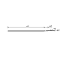
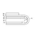
- 1 is a schematic side view of a display device according to an embodiment of the present invention.
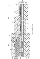
- FIG. 3 is an enlarged view of a cross section taken along line III-III of the display device shown in FIG. It is the top view which expanded a part of touch electrode. It is a figure which shows a 1st pad and a 2nd pad. It is a top view which shows the modification of a touch electrode. It is a figure which shows the bending state of the display apparatus of embodiment which applied this invention. It is a figure which shows the usage form of the display apparatus of embodiment which applied this invention. It is an enlarged view of the part shown by IX in FIG. FIG.
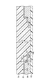
- 10 is a cross-sectional view of the structure shown in FIG. 9 taken along the line XX.
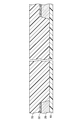
- 10 is a cross-sectional view taken along line XI-XI of the structure shown in FIG. 9;
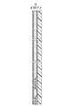
- 10 is a cross-sectional view taken along line XII-XII of the structure shown in FIG.
- It is a figure explaining the manufacturing method of the display concerning a embodiment of the present invention. It is a figure explaining the manufacturing method of the display concerning a embodiment of the present invention. It is a figure explaining the manufacturing method of the display concerning a embodiment of the present invention. It is a figure explaining the manufacturing method of the display concerning a embodiment of the present invention. It is a figure explaining the manufacturing method of the display concerning a embodiment of the present invention. It is a figure explaining the manufacturing method of the display concerning a embodiment of the present invention. It is a figure explaining the manufacturing method of the display concerning a embodiment of the present invention.
- FIG. 1 is a schematic plan view of a display device according to an embodiment of the present invention.
- FIG. 2 is a schematic side view of a display device according to an embodiment of the present invention.
- the display device is an organic electroluminescent display device.
- the display device combines, for example, unit pixels (sub-pixels) of a plurality of colors of red, green and blue to form a full-color pixel (pixel), and displays a full-color image in the display area DA.
- the flexible printed circuit board FP is connected to the display device. On the flexible printed circuit board FP, an integrated circuit chip IC for driving an element for displaying an image is mounted.
- FIG. 3 is an enlarged view of a cross section taken along line III-III of the display shown in FIG.
- the display device has a flexible substrate 10.
- the flexible substrate 10 has a width in the first direction D1 shown in FIG. 1 and a length in the second direction D2 orthogonal to the first direction D1.
- the flexible substrate 10 has a first area A1 including the display area DA.
- the display circuit layer 12 for displaying an image is stacked in the first area A1.
- the flexible substrate 10 has a second area A2 adjacent to the first area A1 in the second direction D2.
- An undercoat layer 14 made of an inorganic insulating material is formed on the flexible substrate 10 as a barrier to impurities, and a semiconductor layer 16 is formed thereon.
- the source electrode 18 and the drain electrode 20 are electrically connected to the semiconductor layer 16, and the gate insulating film 22 made of an inorganic insulating material is formed to cover the semiconductor layer 16.
- a gate electrode 24 is formed on the gate insulating film 22, and an interlayer insulating film 26 made of an inorganic insulating material is formed to cover the gate electrode 24.
- the source electrode 18 and the drain electrode 20 penetrate the gate insulating film 22 and the interlayer insulating film 26.
- the semiconductor layer 16, the source electrode 18, the drain electrode 20 and the gate electrode 24 constitute at least a part of the thin film transistor TFT.
- the undercoat layer 14, the gate insulating film 22 and the interlayer insulating film 26 disposed in the first region A1 extend to the second region A2.
- the undercoat layer 14, the gate insulating film 22 and the interlayer insulating film 26 are stacked, and if necessary, other inorganic insulating films are added to form a first inorganic insulating film made entirely of an inorganic insulating material.
- the membrane 28 is configured.
- the first inorganic insulating film 28 is composed of a plurality of insulating layers.
- a planarization layer 30 is provided on the interlayer insulating film 26 so as to cover the thin film transistor TFT.
- the planarization layer 30 is made of an organic insulating material.
- the planarization layer 30 is provided in the first area A1 in which the display circuit layer 12 is stacked, but is not provided in the second area A2.
- a second inorganic insulating film 32 interposed between a pair of electrodes constituting a capacity for holding an image signal is laminated.
- the second inorganic insulating film 32 is in contact with the underlying interlayer insulating film 26 so as to overlap the planarization layer 30. That is, the planarization layer 30 having high moisture permeability is shielded from moisture by being sandwiched between the second inorganic insulating film 32 and the interlayer insulating film 26 having low moisture permeability.
- a plurality of pixel electrodes 34 (for example, anodes) configured to correspond to the plurality of unit pixels are provided.
- the pixel electrode 34 is one of a pair of electrodes for forming the above-described capacitance.
- the planarizing layer 30 is formed so that at least the surface of the second inorganic insulating film 32 on which the pixel electrode 34 is provided is flat.
- the pixel electrode 34 penetrates the second inorganic insulating film 32 and the planarization layer 30 and is electrically connected to one of the source electrode 18 and the drain electrode 20 on the semiconductor layer 16.
- a bank layer 36 made of an organic insulating material is formed on the second inorganic insulating film 32 and the pixel electrode 34.
- the bank layer 36 is mounted on the peripheral portion of the pixel electrode 34 and is formed so as to open a part (for example, the central portion) of the pixel electrode 34.
- the bank layer 36 forms a bank surrounding a part of the pixel electrode 34.
- the pixel electrode 34 is a part of the light emitting element 38.
- the light emitting element 38 further includes a counter electrode 40 (for example, a cathode) facing the plurality of pixel electrodes 34 and a light emitting layer 42.
- the light emitting layer 42 is provided separately (separately) for each pixel electrode 34, and is also placed on the bank layer 36.
- the light emitting layer 42 emits light in blue, red or green corresponding to each pixel.
- the color corresponding to each pixel is not limited to this, and may be yellow or white, for example.
- the light emitting layer 42 is formed, for example, by vapor deposition.
- the light emitting layer 42 may be formed on the entire surface covering the display area DA so as to extend over the plurality of pixel electrodes 34. That is, the light emitting layer 42 may be formed continuously on the bank layer 36.
- the light emitting layer 42 is formed by application by solvent dispersion. When the light emitting layer 42 is formed so as to extend across the plurality of pixel electrodes 34, it emits white light in all sub-pixels, and extracts a desired color wavelength portion through a color filter (not shown).
- At least one of a hole injection layer and a hole transport layer (not shown) is interposed between the pixel electrode 34 and the light emitting layer 42.
- the hole injection layer or the hole transport layer may be provided separately for each pixel electrode 34, but may be continuous over the entire display area DA shown in FIG.
- the hole injection layer is in contact with the pixel electrode 34 and the bank layer 36.
- At least one of an electron injection layer and an electron transport layer (not shown) is interposed between the counter electrode 40 and the light emitting layer 42.
- the electron injection layer or the electron transport layer may be provided separately for each pixel electrode 34, but may be continuous over the entire display area DA shown in FIG.
- the electron injection layer contacts the counter electrode 40.
- the light emitting layer 42 is sandwiched between the pixel electrode 34 and the counter electrode 40, and the luminance is controlled by the current flowing between the two to emit light.
- the counter electrode 40 is made of a metal thin film or the like and has light transparency, and transmits light generated by the light emitting layer 42 to display an image.
- the pixel electrode 34 includes a reflective film that reflects light generated in the light emitting layer 42 in the direction of the counter electrode 40, the lowermost layer of the plurality of layers is a reflective film, and the layer above it is a transparent conductive film, It is also good.
- the light emitting element 38 is sealed by the sealing layer 44 and blocked from moisture.
- the sealing layer 44 has a structure in which a pair of inorganic films 46 a and 46 b made of an inorganic material such as silicon nitride sandwiches the organic film 48. At least one of the pair of inorganic films 46 a and 46 b is provided so as to exceed the bank layer 36 and is in contact with the underlying second inorganic insulating film 32 so as to overlap. That is, the bank layer 36 having high moisture permeability is shielded from moisture by being sandwiched by at least one of the inorganic films 46 a and 46 b having low moisture permeability and the second inorganic insulating film 32.
- the inorganic films 46 a and 46 b cover up to the end of the planarization layer 30 to block moisture and oxygen.
- the organic layer 50 is used as a mask when etching the inorganic films 46a and 46b, the tips thereof are aligned with each other.
- the display circuit layer 12 includes an element for displaying an image.
- the display circuit layer 12 is provided with a touch electrode 52 for performing touch sensing via the organic layer 50.
- FIG. 4 is an enlarged plan view of a part of the touch electrode 52.
- the touch electrode 52 has a first pad 54 and a second pad 56.
- One of the first pad 54 and the second pad 56 is on the side that transmits the touch sensing signal, and the other is on the side that receives the touch sensing signal.
- the adjacent first pads 54 or the adjacent second pads 56 are connected by the connection wiring 58.
- the first pads 54 adjacent to each other or the second pads 56 adjacent to each other (second pads 56 in this example) are connected by the jumper wiring 60.
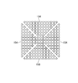
- FIG. 5 is a view showing the first pad 54 and the second pad 56.
- the external shape of each of the first pad 54 and the second pad 56 is diamond-shaped or rectangular. Since the first pad 54 and the second pad 56 are in the same layer, the optical path lengths become equal when the incident external light is reflected, so that the difference in reflection hardly appears and it is difficult to be visually recognized visually. Further, each of the first pad 54 and the second pad 56 is formed in a mesh shape, and the light emitting elements 38 are arranged in a mesh. Therefore, even if the first pad 54 and the second pad 56 are formed of metal, light is not blocked. A dummy electrode (not shown) which is not electrically connected to any of the adjacent first pads 54 and second pads 56 may be disposed. By doing so, the capacitive coupling of the first pad 54 and the second pad 56 can be appropriately reduced, and as a result, the capacitance change due to touch can be made relatively large.
- the touch interlayer insulating film 62 is interposed between the layer forming the first pad 54 and the second pad 56 and the layer forming the jumper wiring 60.
- the touch wiring 64 is connected to the touch electrode 52 through the touch interlayer insulating film 62.
- the touch wiring 64 is provided on the touch interlayer insulating film 62 and is in the same layer as the jumper wiring 60.
- FIG. 6 is a plan view showing a modification of the touch electrode.
- the plurality of first pads 154 and the plurality of second pads 156 are in different layers, and the touch interlayer insulating film is interposed therebetween.
- process defects such as opening failure and generation of particles are less likely to occur.
- the front lamination film 66 is attached via the adhesive layer 63 so as to cover the touch electrode 52, and the polarizing plate 68 is attached thereon.
- the adhesive layer 63 is provided on the touch interlayer insulating film 62, has a thickness for planarizing the unevenness of the surface of the touch interlayer insulating film 62, and has a flat upper surface.
- a back lamination film 70 is attached in the first area A1, and a heat diffusion sheet 72 is attached below the back lamination film 70.
- the back lamination film 70 is also stuck to the second region A2 at a position overlapping at least a connection portion with the flexible printed circuit board FP.
- a plurality of wirings 74 are stacked in the second area A2.
- the plurality of wires 74 extend from the first region A1 in the second direction D2.
- the plurality of wires 74 are arranged in the first direction D1 so as not to be electrically connected to each other (see FIG. 9).
- the plurality of wires 74 include wires connected to the touch electrode 52.
- the wiring 74 illustrated in FIG. 3 is connected to the touch wiring 64.
- the second inorganic insulating film 32 extends so as to be interposed between the touch wiring 64 and the wiring 74, and the touch wiring 64 is formed via the opening 32a of the second inorganic insulating film 32.
- the wiring 74 are electrically connected.
- a transparent conductive film 75 such as ITO (Indium Tin Oxide) is interposed between the touch electrode 64 and the wiring 74.
- the transparent conductive film 75 is formed simultaneously with the film that constitutes a part of the pixel electrode 34.
- An organic insulating film 76 is placed above the second inorganic insulating film 32.
- the plurality of wires 74 are electrically connected to the flexible printed circuit board FP at the end. The electrical connection is made by the conductive particles 77a by using the anisotropic conductive film 77, and the mechanical connection is made by the thermosetting resin 77b.
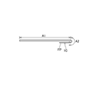
- FIG. 7 is a view showing a bent state of the display device of the embodiment to which the present invention is applied.
- the display device is adapted to be bent.
- the second region A2 (except for the junction with the flexible printed circuit board FP) of the flexible substrate 10 shown in FIG. 3 is bent.
- part of the display device can be overlapped and miniaturized, and the flexible printed circuit board FP can be disposed on the back side of the display device.
- FIG. 8 is a view showing a usage pattern of the display device of the embodiment to which the present invention is applied.
- the display device has a main body B including the flexible substrate 10 and the display circuit layer 12 and a plurality of wirings 74.
- a front lamination film 66 and a polarizing plate 68 are provided on the front side of the main body B in the first region A1.
- An organic insulating film 76 is provided in the second region A2 adjacent to these.
- the main body B (flexible substrate 10) bends around an axis AX extending in the first direction D1.
- the spacer 90 is disposed on the inside of the bend to restrict the curvature from becoming too large.
- a back lamination film 70 is attached except for at least a bending portion.
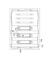
- FIG. 9 is an enlarged view of a portion shown by IX in FIG.
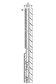
- FIG. 10 is a cross-sectional view taken along line XX of the structure shown in FIG.
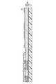
- FIG. 11 is a cross-sectional view taken along line XI-XI of the structure shown in FIG.
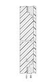
- FIG. 12 is a cross-sectional view taken along line XII-XII of the structure shown in FIG.
- the first inorganic insulating film 28 is located under the plurality of wires 74.
- the lower ground of the plurality of wires 74 is configured of the flexible substrate 10 and the first inorganic insulating film 28.
- the lower ground of the plurality of wires 74 has a step ST in the second area A2.
- the stepped portion ST is formed.
- the stepped portion ST has a plurality of steps.
- the stepped portion ST includes a plurality of upper surfaces 78 adjacent to each other in the second direction D2 at different heights.
- the lowest surfaces 78 ⁇ / b> L of the plurality of upper surfaces 78 are part of the upper surface 78 of the flexible substrate 10.
- the stepped portion ST includes a kick surface 80 rising from the plurality of top surfaces 78 except the top surface 78U.
- the first inorganic insulating film 28 constitutes at least a plurality of upper surfaces 78 excluding the lower surface 78L and the kick surface 80.
- each of the plurality of upper surfaces 78 excluding the uppermost surface 78U and the kicking surface 80 form an entrance corner 82.
- Each wire 74 has a convex portion 84 projecting in the direction opposite to the adjacent wire 74 (see FIGS. 9 and 11).
- the convex portion 84 protrudes in the first direction D1 along the entrance angle portion 82.
- the pair of convex portions 84 of the adjacent wires 74 project in directions opposite to each other.
- the pair of projections 84 are spaced apart and electrically insulated (see FIG. 9).
- the convex portion 84 is an etching residue when the conductive film 86 described later is etched to form a plurality of wirings 74.
- the second inorganic insulating film 32 is on the plurality of wires 74.
- the second inorganic insulating film 32 is provided at least in the step portion ST so as to avoid the region R continuous in the second direction D2 between the adjacent wirings 74.
- the region R where the second inorganic insulating film 32 is not provided is a portion removed from the inorganic film 88 described later by etching.
- the etching residue of the conductive film 86 existing therebelow is also removed along with the inorganic film 88 (details will be described later). Thereby, an interval is formed between the pair of convex portions 84 described above.
- the region R avoided by the second inorganic insulating film 32 is continuous over the entire length in the second direction D2 between the adjacent wires 74, as defined by the lower surfaces 78L of the plurality of upper surfaces 78 (see FIG. 9). .
- the second inorganic insulating film 32 is provided on the lowest surface 78 L of the plurality of upper surfaces 78 so as to avoid overlapping with at least a portion of each of the plurality of interconnections 74.
- the second inorganic insulating film 32 is provided so as to avoid the region R covering the entire width in the first direction D1, when limited to the lower surfaces 78L of the plurality of upper surfaces 78.
- An organic insulating film 76 is on the second inorganic insulating film 32.
- the organic insulating film 76 is in contact with the base surface in a region R which the second inorganic insulating film 32 avoids.
- the organic insulating film 76 intervenes between the pair of convex portions 84 to prevent shorting of the adjacent wires 74.
- FIG. 13 to 17 are views for explaining a method of manufacturing a display device according to an embodiment of the present invention.
- a laminated structure up to the first inorganic insulating film 28 is formed on the flexible substrate 10.
- the first inorganic insulating film 28 is composed of a plurality of layers (the undercoat layer 14, the gate insulating film 22 and the interlayer insulating film 26) as shown in FIG. 3, and is patterned by etching to which photolithography is applied.
- the patterned first inorganic insulating film 28 constitutes at least a part of the stepped portion ST, as shown in FIGS.
- a conductive film 86 is formed on the first inorganic insulating film 28, and as shown in FIG. 15, the conductive film 86 is patterned to form a plurality of wirings 74.
- the patterning is performed by etching applying photolithography. Note that the source electrode 18 and the drain electrode 20 are also formed from the conductive film 86.
- the conductive film 86 remains because an etchant (for example, an etching solution) is difficult to enter at the angled portion 82 (see FIGS. 9 to 12) of the step portion ST on the lower ground of the plurality of wires 74. . Therefore, the wires 74 adjacent to each other may short.
- an etchant for example, an etching solution
- the inorganic film 88 is formed so as to cover the plurality of wires 74, and the inorganic film 88 is patterned as shown in FIG. 17.
- the inorganic film 88 is removed from the region R continuous in the second direction D2 between adjacent wires 74 by patterning at least in the step portion ST, thereby forming the second inorganic insulating film 32 (see FIG. 9).
- the conductive film 86 (the portion between the pair of convex portions 84) remaining between the adjacent wires 74 is removed (see FIG. 9). By doing this, the conduction between the adjacent wires 74 can be disconnected. Thereafter, an obvious process is performed from the structure shown in FIG.
- FIG. 18 is a view showing a modification of the structure shown in FIG.
- any one of the plurality of upper surfaces 278 is a part of the upper surface 278 of the first inorganic insulating film 228. That is, the first inorganic insulating film 228 exists below the entire plurality of wirings 274.
- FIG. 19 shows a modification of the structure shown in FIG.
- the second inorganic insulating film 332 is provided so that the plurality of upper surfaces 378 constituting the stepped portion ST also overlap the entire plurality of wires 374.
- FIG. 20 is a diagram showing a modification 1 of the structure shown in FIG.
- the first inorganic insulating film 28 is a process of disconnecting the conduction between the adjacent wires 74, and the portion that protrudes from the second inorganic insulating film 32 is removed.
- the first inorganic insulating film 428 has a portion protruding from the second inorganic insulating film 432.
- the first inorganic insulating film 428 in the portion protruding from the second inorganic insulating film 432 has the second step portion ST2 whose surface is scraped and becomes low. Have.
- the first inorganic insulating film 428 does not have to be completely protruded from the second inorganic insulating film 432.
- FIG. 21 is a diagram showing a modification 2 of the structure shown in FIG.
- the process of cutting the conduction of the adjacent wires 74 is performed by the patterning process of the inorganic film 88 for forming the second inorganic insulating film 32.
- an inorganic film for forming the second inorganic insulating film 532 is formed, and this is patterned. Therefore, the second inorganic insulating film 532 covers the side surface of the first inorganic insulating film 528 and extends beyond the periphery thereof.
- FIG. 21 is a diagram showing a modification 2 of the structure shown in FIG.
- the process of cutting the conduction of the adjacent wires 74 is performed by the patterning process of the inorganic film 88 for forming the second inorganic insulating film 32.
- an inorganic film for forming the second inorganic insulating film 532 is formed, and this is patterned. Therefore, the second inorganic insulating film 532 covers the side surface of the first inorganic
- step 21 since the first inorganic insulating film 528 is etched slightly wider than the place where the step portion ST shown in FIG. 10 or 11 is present, the second step portion ST2 is formed low. In step 11, the number of steps is increased by one in a flat area to form a third step ST3.
- the display device is not limited to the organic electroluminescence display device, and may be a display device provided with a light emitting element such as a quantum dot light emitting element (QLED: Quantum-Dot Light Emitting Diode) in each pixel. Or a liquid crystal display device.
- a light emitting element such as a quantum dot light emitting element (QLED: Quantum-Dot Light Emitting Diode) in each pixel.
- QLED Quantum-Dot Light Emitting Diode
- the present invention is not limited to the above-described embodiment, and various modifications are possible.
- the configurations described in the embodiments can be replaced with configurations that have substantially the same configuration, configurations having the same effects, or configurations that can achieve the same purpose.
Landscapes
- Engineering & Computer Science (AREA)
- Physics & Mathematics (AREA)
- Theoretical Computer Science (AREA)
- General Physics & Mathematics (AREA)
- General Engineering & Computer Science (AREA)
- Human Computer Interaction (AREA)
- Computer Hardware Design (AREA)
- Microelectronics & Electronic Packaging (AREA)
- Nonlinear Science (AREA)
- Power Engineering (AREA)
- Mathematical Physics (AREA)
- Chemical & Material Sciences (AREA)
- Crystallography & Structural Chemistry (AREA)
- Optics & Photonics (AREA)
- Devices For Indicating Variable Information By Combining Individual Elements (AREA)
- Electroluminescent Light Sources (AREA)
Abstract
表示装置は、画像を表示するために第1領域(A1)でフレキシブル基板(10)に積層された表示回路層(12)と、第1領域(A1)から第2方向(D2)に延び、相互に電気的に接続しないように第1方向(D1)に並び、第2領域(A2)でフレキシブル基板(10)に積層する複数の配線(74)と、複数の配線(74)の下でフレキシブル基板(10)に積層する第1無機絶縁膜(28)と、を含む。複数の配線(74)の下地面は、相互に高さが異なって第2方向(D2)に隣り合う複数の上面(78)と、最上面(78U)を除く複数の上面(78)から立ち上がる蹴上面(80)と、を含む階段部(ST)を、第2領域(A2)に有する。第1無機絶縁膜(28)は、少なくとも、最低面(78L)を除く複数の上面(78)及び蹴上面(80)を構成する。隣同士の配線(74)は、第1無機絶縁膜(28)上で分離されている。
Description
本発明は、表示装置に関する。
表示装置として、可撓性を有するフレキシブルディスプレイが開発されている。例えば、可撓性を有する樹脂基板上に回路層及び有機エレクトロルミネッセンス層が形成された表示装置が知られている(特許文献1)。可撓性を有する樹脂基板は、樹脂層をガラス基板の上に形成し、硬化させ、ガラス基板から剥離することで製造していた。
樹脂基板には、絶縁層及び配線層が積層されており、屈曲させる領域から絶縁層を除去することで、フレキシブルディスプレイを曲がりやすくしている。絶縁層は、一部が除去されることで段差が形成される。そのため、絶縁層の上に配線を形成するときに行われる導電膜のエッチングで、隣同士の配線の間に導電膜が残りやすく、ショートの原因になる。
特許文献2には、配線の下に反射板を配置することで、フォトリソグラフィ工程で段差部からレジスト残渣を無くすことが開示されているが、レジスト残渣以外の原因で隣同士の配線の間に導電膜が残った場合の対策が開示されていない。
特許文献3には、層間絶縁膜に開口を形成することが開示されているが、下地面の段差部を下段から上段にわたって配線が通る構造に対応していない。
特許文献4には、厚い層間絶縁膜に凸部を形成することで、その上に形成されるフォトレジストを露光及び洗浄したときのレジスト残渣を無くすことが開示されているが、レジスト残渣以外の原因で隣同士の配線の間に導電膜が残った場合の対策が開示されていない。
本発明は、配線間のショートを防止することを目的とする。
本発明に係る表示装置は、第1方向の幅及び前記第1方向に直交する第2方向の長さを有し、前記第2方向に隣り合うように、第1領域及び第2領域を有するフレキシブル基板と、画像を表示するために前記第1領域で前記フレキシブル基板に積層された表示回路層と、前記第1領域から前記第2方向に延び、相互に電気的に接続しないように前記第1方向に並び、前記第2領域で前記フレキシブル基板に積層する複数の配線と、前記複数の配線の下で前記フレキシブル基板に積層する第1無機絶縁膜と、を含み、前記複数の配線の下地面は、相互に高さが異なって前記第2方向に隣り合う複数の上面と、最上面を除く前記複数の上面から立ち上がる蹴上面と、を含む階段部を持つ前記第1無機絶縁膜と、前記第2領域にて接し、前記第1無機絶縁膜は、少なくとも、最低面を除く前記複数の上面及び前記蹴上面を構成し、隣同士の前記配線は、前記第1無機絶縁膜において前記第2領域の前記階段部が無い箇所にて分離されていることを特徴とする。
本発明によれば、複数の配線を形成するときに階段部に導電膜が残ったとしても、隣同士の配線の導通を切断することができ、配線間のショートを防止することができる。
本発明に係る表示装置は、第1方向の幅及び前記第1方向に直交する第2方向の長さを有し、前記第2方向に隣り合うように、第1領域及び第2領域を有するフレキシブル基板と、画像を表示するために前記第1領域で前記フレキシブル基板に積層された表示回路層と、前記第1領域から前記第2方向に延び、相互に電気的に接続しないように前記第1方向に並び、前記第2領域で前記フレキシブル基板に積層する複数の配線と、前記複数の配線の下で前記フレキシブル基板に積層する第1無機絶縁膜と、を含み、前記複数の配線の下地面は、相互に高さが異なって前記第2方向に隣り合う複数の上面と、最上面を除く前記複数の上面から立ち上がる蹴上面と、を含む階段部を持つ前記第1無機絶縁膜と、前記第2領域にて接し、前記第1無機絶縁膜は、少なくとも、最低面を除く前記複数の上面及び前記蹴上面を構成し、前記第1無機絶縁膜は、それぞれが前記第2領域の前記階段部よりも低く相互に高さが異なって前記第2方向に隣り合う複数の他の上面と、前記複数の他の上面から立ち上がる蹴上面とを含む第2階段部を前記第2領域に持ち、第2階段部にて隣り合う前記複数の配線は切断されている。
以下、本発明の実施形態について図面を参照して説明する。但し、本発明は、その要旨を逸脱しない範囲において様々な態様で実施することができ、以下に例示する実施形態の記載内容に限定して解釈されるものではない。
図面は、説明をより明確にするため、実際の態様に比べ、各部の幅、厚さ、形状等について模式的に表される場合があるが、あくまで一例であって、本発明の解釈を限定するものではない。本明細書と各図において、既出の図に関して説明したものと同様の機能を備えた要素には、同一の符号を付して、重複する説明を省略することがある。
さらに、本発明の詳細な説明において、ある構成物と他の構成物の位置関係を規定する際、「上に」「下に」とは、ある構成物の直上あるいは直下に位置する場合のみでなく、特に断りの無い限りは、間にさらに他の構成物を介在する場合を含むものとする。
図1は、本発明の実施形態に係る表示装置の平面概略図である。図2は、本発明の実施形態に係る表示装置の側面概略図である。表示装置は、有機エレクトロルミネッセンス表示装置である。表示装置は、例えば、赤、緑及び青からなる複数色の単位画素(サブピクセル)を組み合わせて、フルカラーの画素(ピクセル)を形成し、表示領域DAにフルカラーの画像を表示するようになっている。表示装置には、フレキシブルプリント基板FPが接続されている。フレキシブルプリント基板FPには、画像を表示するための素子を駆動するための集積回路チップICが搭載されている。
図3は、図1に示す表示装置のIII-III線断面の拡大図である。表示装置は、フレキシブル基板10を有する。フレキシブル基板10は、図1に示す第1方向D1の幅及び第1方向D1に直交する第2方向D2の長さを有する。フレキシブル基板10は、表示領域DAを含む第1領域A1を有する。第1領域A1には、画像を表示するための表示回路層12が積層されている。フレキシブル基板10は、第2方向D2に第1領域A1に隣り合う第2領域A2を有する。
フレキシブル基板10には、不純物に対するバリアとなるように、無機絶縁材料からなるアンダーコート層14が形成され、その上に半導体層16が形成されている。半導体層16にソース電極18及びドレイン電極20が電気的に接続し、半導体層16を覆って、無機絶縁材料からなるゲート絶縁膜22が形成されている。ゲート絶縁膜22の上にはゲート電極24が形成され、ゲート電極24を覆って、無機絶縁材料からなる層間絶縁膜26が形成されている。ソース電極18及びドレイン電極20は、ゲート絶縁膜22及び層間絶縁膜26を貫通している。半導体層16、ソース電極18、ドレイン電極20及びゲート電極24によって薄膜トランジスタTFTの少なくとも一部が構成される。
第1領域A1に配置されるアンダーコート層14、ゲート絶縁膜22及び層間絶縁膜26は、第2領域A2にも至る。第2領域A2では、アンダーコート層14、ゲート絶縁膜22及び層間絶縁膜26が積層して、必要に応じてその他の無機絶縁膜を加えて、全体的に無機絶縁材料からなる第1無機絶縁膜28が構成される。第1無機絶縁膜28は、複数の絶縁層からなる。
第1領域A1では、層間絶縁膜26の上には、薄膜トランジスタTFTを覆うように、平坦化層30が設けられている。平坦化層30は、有機絶縁材料からなる。平坦化層30は、表示回路層12が積層される第1領域A1に設けられるが、第2領域A2には設けられないようになっている。平坦化層30の上には、画像信号を保持するための容量を構成する一対の電極の間に介在する第2無機絶縁膜32が積層している。第2無機絶縁膜32は、平坦化層30を超えて、その下の層間絶縁膜26に接触して重なる。つまり、透湿性の高い平坦化層30は、透湿性の低い第2無機絶縁膜32及び層間絶縁膜26に挟まれることで、水分から遮断されている。
第2無機絶縁膜32の上には、複数の単位画素それぞれに対応するように構成された複数の画素電極34(例えば陽極)が設けられている。画素電極34は、上述した容量を構成するための一対の電極の一方である。平坦化層30は、第2無機絶縁膜32において少なくとも画素電極34が設けられる面が平坦になるように形成される。画素電極34は、第2無機絶縁膜32及び平坦化層30を貫通して、半導体層16上のソース電極18及びドレイン電極20の一方に電気的に接続している。
第2無機絶縁膜32及び画素電極34上に、有機絶縁材料からなるバンク層36が形成されている。バンク層36は、画素電極34の周縁部に載り、画素電極34の一部(例えば中央部)を開口させるように形成されている。バンク層36によって、画素電極34の一部を囲むバンクが形成される。画素電極34は、発光素子38の一部である。発光素子38は、複数の画素電極34に対向する対向電極40(例えば陰極)と発光層42をさらに含む。
発光層42は、画素電極34ごとに別々に(分離して)設けられ、バンク層36にも載るようになっている。この場合は各画素に対応して青、赤又は緑で発光層42が発光するようになる。各画素に対応する色はこれに限られず、例えば、黄又は白等でもよい。発光層42は、例えば、蒸着により形成される。あるいは、発光層42は、表示領域DAを覆う全面に、複数の画素電極34に亘るように形成してもよい。つまり、発光層42をバンク層36上で連続するように形成してもよい。この場合、発光層42は溶媒分散による塗布により形成する。発光層42を複数の画素電極34に亘るように形成する場合は、全サブピクセルにおいて白色で発光し、図示しないカラーフィルタを通して所望の色波長部分を取り出す構成になる。
画素電極34と発光層42との間に、図示しない正孔注入層及び正孔輸送層の少なくとも一方が介在する。正孔注入層又は正孔輸送層は、1つの画素電極34ごとに分離して設けてもよいが、図1に示す表示領域DAの全体にわたって連続してもよい。正孔注入層は、画素電極34及びバンク層36に接触する。
対向電極40と発光層42との間に、図示しない電子注入層及び電子輸送層の少なくとも一方が介在する。電子注入層又は電子輸送層は、1つの画素電極34ごとに分離して設けてもよいが、図1に示す表示領域DAの全体にわたって連続してもよい。電子注入層は、対向電極40に接触する。
発光層42は、画素電極34及び対向電極40に挟まれ、両者間を流れる電流によって輝度が制御されて発光する。対向電極40は、金属薄膜などからなり光透過性を有し、発光層42で生じた光を透過させて画像を表示する。画素電極34は、発光層42で生じた光を対向電極40の方向に反射する反射膜を含み、複数層の最下層が反射膜であり、それよりも上の層が透明導電膜であってもよい。
発光素子38は、封止層44によって封止されて水分から遮断される。封止層44は、窒化ケイ素などの無機材料からなる一対の無機膜46a,46bが有機膜48を挟む構造になっている。一対の無機膜46a,46bの少なくとも一方は、バンク層36を超えるように設けられて、その下の第2無機絶縁膜32に接触して重なる。つまり、透湿性の高いバンク層36は、透湿性の低い無機膜46a,46bの少なくとも一方及び第2無機絶縁膜32に挟まれることで、水分から遮断される。無機膜46a、46bは平坦化層30の端部までを覆って水分や酸素を遮断するようになっている。また、有機層50は、無機膜46a、46bをエッチングするときに、マスクとして使用されるので、無機膜46a、46bと先端がそろうようになっている。以上説明したように、画像を表示するための素子を表示回路層12は含む。表示回路層12には、有機層50を介して、タッチセンシングを行うためにタッチ電極52が設けられている。
図4は、タッチ電極52の一部を拡大した平面図である。タッチ電極52は、第1パッド54と第2パッド56を有する。第1パッド54及び第2パッド56のいずれか一方は、タッチセンシング信号を送信する側にあり、他方は、タッチセンシング信号を受信する側にある。隣同士の第1パッド54又は隣同士の第2パッド56(この例では第1パッド54)は、接続配線58で接続されている。隣同士の第1パッド54又は隣同士の第2パッド56(この例では第2パッド56)は、ジャンパ配線60で接続されている。
図5は、第1パッド54及び第2パッド56を示す図である。第1パッド54及び第2パッド56のそれぞれの外形は、ダイヤモンド形状又は矩形になっている。第1パッド54及び第2パッド56は、同一層にあるので入射した外光が反射したときに光路長が等しくなり、反射の差が表れにくく、光学的に視認されにくい。また、第1パッド54及び第2パッド56のそれぞれは、メッシュ状に形成され、網目の中に発光素子38が配列される。したがって、第1パッド54及び第2パッド56を金属で形成しても、光が遮断されないようになっている。なお、隣り合う第1パッド54及び第2パッド56の間に、いずれにも電気的に接続しないダミー電極(図示せず)を配置してもよい。そうすることで、第1パッド54及び第2パッド56の容量性カップリングを適度に小さくでき、その結果、タッチによる容量変化を相対的に大きくすることができる。
第1パッド54及び第2パッド56を構成する層とジャンパ配線60を構成する層との間に、図3に示すように、タッチ層間絶縁膜62が介在する。タッチ層間絶縁膜62を貫通して、タッチ電極52にタッチ配線64が接続する。タッチ配線64は、タッチ層間絶縁膜62の上に設けられ、ジャンパ配線60と同一層にある。
図6は、タッチ電極の変形例を示す平面図である。この例では、複数の第1パッド154と複数の第2パッド156が異なる層にあり、両者間にタッチ層間絶縁膜が介在する。この構造では、ジャンパ配線を接続するためのコンタクトを開口する必要がないため、開口不良やパーティクルの発生などの工程上の不良が生じにくい。
図3に示すように、第1領域A1では、タッチ電極52を覆うように、接着層63を介して表ラミネーションフィルム66が貼り付けられ、その上に偏光板68が貼り付けられている。接着層63は、タッチ層間絶縁膜62の上に設けられ、タッチ層間絶縁膜62の表面の凹凸を平坦化する厚みを有し、上面が平らである。フレキシブル基板10の裏面には、第1領域A1で、裏ラミネーションフィルム70が貼り付けられ、その下に熱拡散シート72が貼り付けられている。裏ラミネーションフィルム70は、第2領域A2にも、少なくともフレキシブルプリント基板FPとの接続部と重なる位置に貼り付けられている。
フレキシブル基板10には、第2領域A2に、複数の配線74が積層されている。複数の配線74は、第1領域A1から第2方向D2に延びる。複数の配線74は、相互に電気的に接続しないように、第1方向D1に並ぶ(図9参照)。複数の配線74は、タッチ電極52に接続される配線を含む。例えば、図3に示す配線74は、タッチ配線64に接続される。詳しくは、第2領域A2では、第2無機絶縁膜32が、タッチ配線64と配線74の間に介在するように延びており、第2無機絶縁膜32の開口32aを介して、タッチ配線64と配線74が電気的に接続するようになっている。なお、タッチ電極64と配線74の間には、ITO(Indium Tin Oxide)などの透明導電膜75が介在している。透明導電膜75は、画素電極34の一部を構成する膜と同時に形成されるものである。第2無機絶縁膜32の上方には、有機絶縁膜76が載っている。複数の配線74は、端部でフレキシブルプリント基板FPに電気的に接続する。電気的接続は、異方性導電フィルム77を使用することで導電粒子77aによってなされ、熱硬化性樹脂77bによって機械的接続が図られる。
図7は、本発明を適用した実施形態の表示装置の屈曲状態を示す図である。図7に示すように、表示装置は、屈曲させられるようになっている。詳しくは、図3に示すフレキシブル基板10の第2領域A2(フレキシブルプリント基板FPとの接合部を除く)が屈曲する。屈曲により、表示装置の一部を重ねて小型化することができ、フレキシブルプリント基板FPを表示装置の裏側に配置することも可能になる。
図8は、本発明を適用した実施形態の表示装置の使用形態を示す図である。表示装置は、フレキシブル基板10及び表示回路層12並びに複数の配線74を含む本体Bを有する。第1領域A1では、本体Bの表側に、表ラミネーションフィルム66及び偏光板68が設けられている。これらに隣接して、第2領域A2には有機絶縁膜76が設けられている。本体B(フレキシブル基板10)は、第1方向D1に延びる軸AXの周りに屈曲する。屈曲の内側にスペーサ90が配置されており、曲率が大きくなり過ぎないよう規制している。本体Bの裏側には、少なくとも屈曲する部分を除いて、裏ラミネーションフィルム70が貼り付けられている。
図9は、図1にIXで示す部分の拡大図である。図10は、図9に示す構造のX-X線断面図である。図11は、図9に示す構造のXI-XI線断面図である。図12は、図9に示す構造のXII-XII線断面図である。
複数の配線74の下には第1無機絶縁膜28がある。本実施形態では、複数の配線74の下地面は、フレキシブル基板10及び第1無機絶縁膜28から構成されている。フレキシブル基板10から構成される下地面には、第1無機絶縁膜28が存在しない領域がある(図10参照)。硬い第1無機絶縁膜28を設けないことで、フレキシブル基板10が屈曲しやすくなっている。
複数の配線74の下地面は、第2領域A2に階段部STを有する。第1無機絶縁膜28の一部を除去するときに階段部STが形成される。第1無機絶縁膜28が複数層からなるときには、階段部STは複数段になる。階段部STは、相互に高さが異なって第2方向D2に隣り合う複数の上面78を含む。複数の上面78の最低面78Lは、フレキシブル基板10の上面78の一部である。階段部STは、最上面78Uを除く複数の上面78から立ち上がる蹴上面80を含む。第1無機絶縁膜28は、少なくとも、最低面78Lを除く複数の上面78及び蹴上面80を構成する。階段部STにおいて、最上面78Uを除く複数の上面78のそれぞれと蹴上面80によって、入角部82が構成される。
それぞれの配線74は、隣の配線74に対向する方向に突出する凸部84を有する(図9及び図11参照)。凸部84は、入角部82に沿って第1方向D1に突出する。隣同士の配線74が有する一対の凸部84が、相互に対向する方向に突出する。一対の凸部84は、間隔があいて電気的に絶縁されている(図9参照)。凸部84は、後述する導電膜86をエッチングして複数の配線74を形成するときの、エッチング残りである。
複数の配線74の上には第2無機絶縁膜32がある。第2無機絶縁膜32は、少なくとも階段部STでは、隣同士の配線74の間で第2方向D2に連続する領域Rを避けて設けられている。第2無機絶縁膜32が設けられない領域Rは、後述する無機膜88からエッチングによって除去される部分である。第2無機絶縁膜32が除去される領域Rでは、その下に存在していた導電膜86のエッチング残りも、無機膜88とともに除去される(詳しくは後述する)。これにより、上述した一対の凸部84の間に間隔が形成される。
第2無機絶縁膜32が避ける領域Rは、複数の上面78の最低面78Lに限定して言えば、隣同士の配線74の間で、第2方向D2の全長にわたって連続する(図9参照)。第2無機絶縁膜32は、複数の上面78の最低面78Lでは、複数の配線74のそれぞれの少なくとも一部との重複を避けるように設けられている。第2無機絶縁膜32は、複数の上面78の最低面78Lに限定して言えば、第1方向D1の全幅にわたる領域Rを避けるように設けられている。
第2無機絶縁膜32の上に有機絶縁膜76がある。有機絶縁膜76は、第2無機絶縁膜32が避ける領域Rで下地面に接触する。一対の凸部84の間に有機絶縁膜76が介在して、隣同士の配線74のショートを防止している。
図13~図17は、本発明の実施形態に係る表示装置の製造方法を説明する図である。図13に示すように、フレキシブル基板10には、第1無機絶縁膜28までの積層構造を形成する。第1無機絶縁膜28は、図3に示すように複数層(アンダーコート層14、ゲート絶縁膜22、層間絶縁膜26)からなり、フォトリソグラフィを適用したエッチングによってパターニングする。パターニングされた第1無機絶縁膜28は、図10~12に示すように、階段部STの少なくとも一部を構成する。
図14に示すように、第1無機絶縁膜28に導電膜86を形成し、図15に示すように、導電膜86をパターニングして複数の配線74を形成する。パターニングは、フォトリソグラフィを適用したエッチングによって行う。なお、導電膜86からソース電極18及びドレイン電極20も形成する。この時点では、複数の配線74の下地面にある階段部STの入角部82(図9~図12参照)には、エッチャント(例えばエッチング液)が入りにくいため、導電膜86が残ってしまう。そのため、隣同士の配線74がショートすることがある。
図16に示すように、複数の配線74を覆うように無機膜88を形成し、図17に示すように、無機膜88をパターニングする。パターニングによって、少なくとも階段部STでは、隣同士の配線74の間で第2方向D2に連続する領域Rから無機膜88を除去して、第2無機絶縁膜32を形成する(図9参照)。無機膜88の除去に連続して、隣同士の配線74の間に残った導電膜86(一対の凸部84の間にある部分)を除去する(図9参照)。こうすることで、隣同士の配線74の導通を切断することができる。その後、図3に示す構造から自明なプロセスを行う。
図18は、図10に示す構造の変形例を示す図である。この例では、複数の上面278のいずれもが、第1無機絶縁膜228の上面278の一部である。つまり、複数の配線274の全体にわたって、第1無機絶縁膜228が下に存在している。
図19は、図9に示す構造の変形例を示す図である。この例では、第2無機絶縁膜332は、階段部STを構成する複数の上面378でも、複数の配線374の全体と重複するように設けられている。
図20は、図12に示す構造の変形例1を示す図である。図12の例では、第1無機絶縁膜28は、隣同士の配線74の導通を切断するときのプロセスで、第2無機絶縁膜32からはみ出す部分が除去されている。これに対して、図20の例では、第1無機絶縁膜428は、第2無機絶縁膜432からはみ出す部分を有する。ただし、隣同士の配線74の導通を切断するときのプロセスで、第2無機絶縁膜432からはみ出す部分では、第1無機絶縁膜428は、その表層が削れて低くなった第2階段部ST2を有する。このように、第1無機絶縁膜428は、第2無機絶縁膜432から完全にはみ出さないようにする必要はない。
図21は、図12に示す構造の変形例2を示す図である。図12の例では、隣同士の配線74の導通を切断するときのプロセスを、第2無機絶縁膜32を形成するための無機膜88のパターニングプロセスで行った。これに対して、図21の例では、隣同士の配線74の導通を切断した後に、第2無機絶縁膜532を形成するための無機膜を形成し、これをパターニングする。そのため、第2無機絶縁膜532は、第1無機絶縁膜528の側面を覆い、その周縁を超えるようになっている。図21の例では、図10又は図11に示す階段部STがある個所よりも少し広めに第1無機絶縁膜528がエッチングされるので、第2階段部ST2が低く形成され、図10又は図11では平坦な領域に段数が1段増えて第3階段部ST3が形成される。
なお、表示装置は、有機エレクトロルミネッセンス表示装置には限定されず、量子ドット発光素子(QLED:Quantum‐Dot Light Emitting Diode)のような発光素子を各画素に備えた表示装置であってもよいし、液晶表示装置であってもよい。
本発明は、上述した実施形態に限定されるものではなく種々の変形が可能である。例えば、実施形態で説明した構成は、実質的に同一の構成、同一の作用効果を奏する構成又は同一の目的を達成することができる構成で置き換えることができる。
Claims (14)
- 第1方向の幅及び前記第1方向に直交する第2方向の長さを有し、前記第2方向に隣り合うように、第1領域及び第2領域を有するフレキシブル基板と、
画像を表示するために前記第1領域で前記フレキシブル基板に積層された表示回路層と、
前記第1領域から前記第2方向に延び、相互に電気的に接続しないように前記第1方向に並び、前記第2領域で前記フレキシブル基板に積層する複数の配線と、
前記複数の配線の下で前記フレキシブル基板に積層する第1無機絶縁膜と、
を含み、
前記複数の配線の下地面は、相互に高さが異なって前記第2方向に隣り合う複数の上面と、最上面を除く前記複数の上面から立ち上がる蹴上面と、を含む階段部を持つ前記第1無機絶縁膜と、前記第2領域にて接し、
前記第1無機絶縁膜は、少なくとも、最低面を除く前記複数の上面及び前記蹴上面を構成し、
隣同士の前記配線は、前記第1無機絶縁膜において前記第2領域の前記階段部が無い箇所にて分離されていることを特徴とする表示装置。 - 請求項1に記載された表示装置において、
前記複数の配線は、隣同士の前記配線から相互に対向する方向に突出する一対の凸部を有し、
前記一対の凸部は、間隔があいて電気的に絶縁されていることを特徴とする表示装置。 - 請求項2に記載された表示装置において、
前記一対の凸部は、前記最上面を除く前記複数の上面のそれぞれと前記蹴上面とで構成される入角部に沿って前記第1方向に突出することを特徴とする表示装置。 - 請求項1に記載された表示装置において、
前記複数の上面の前記最低面は、前記フレキシブル基板の上面の一部であることを特徴とする表示装置。 - 請求項1に記載された表示装置において、
前記複数の上面のいずれもが、前記第1無機絶縁膜の上面の一部であることを特徴とする表示装置。 - 請求項1に記載された表示装置において、
前記複数の配線の上で前記フレキシブル基板に積層する第2無機絶縁膜をさらに有し、
前記第2無機絶縁膜は、少なくとも前記階段部では、隣同士の前記配線の間で前記第2方向に連続する領域を避けて設けられることを特徴とする表示装置。 - 請求項6に記載された表示装置において、
前記第2無機絶縁膜が避ける前記領域は、前記複数の上面の前記最低面では、隣同士の前記配線の間で、前記第2方向の全長にわたって連続することを特徴とする表示装置。 - 請求項6に記載された表示装置において、
前記第2無機絶縁膜は、前記複数の上面の前記最低面では、前記複数の配線のそれぞれの少なくとも一部との重複を避けるように設けられていることを特徴とする表示装置。 - 請求項8に記載された表示装置において、
前記第2無機絶縁膜は、前記複数の上面の前記最低面では、前記第1方向の全幅にわたる領域を避けるように設けられていることを特徴とする表示装置。 - 請求項6に記載された表示装置において、
前記第2無機絶縁膜は、前記複数の上面では、前記複数の配線の全体と重複するように設けられていることを特徴とする表示装置。 - 請求項1に記載された表示装置において、
前記第2無機絶縁膜の上で前記フレキシブル基板に積層する有機絶縁膜をさらに有し、
前記有機絶縁膜は、前記第2無機絶縁膜が避ける前記領域で前記下地面に接触することを特徴とする表示装置。 - 請求項1に記載された表示装置において、
前記第1無機絶縁膜は、複数の絶縁層からなり、
前記階段部は、複数段になるように構成されていることを特徴とする表示装置。 - 請求項1に記載された表示装置において、
前記フレキシブル基板は、前記第1方向に延びる軸AXの周りに屈曲していることを特徴とする表示装置。 - 第1方向の幅及び前記第1方向に直交する第2方向の長さを有し、前記第2方向に隣り合うように、第1領域及び第2領域を有するフレキシブル基板と、
画像を表示するために前記第1領域で前記フレキシブル基板に積層された表示回路層と、
前記第1領域から前記第2方向に延び、相互に電気的に接続しないように前記第1方向に並び、前記第2領域で前記フレキシブル基板に積層する複数の配線と、
前記複数の配線の下で前記フレキシブル基板に積層する第1無機絶縁膜と、
を含み、
前記複数の配線の下地面は、相互に高さが異なって前記第2方向に隣り合う複数の上面と、最上面を除く前記複数の上面から立ち上がる蹴上面と、を含む階段部を持つ前記第1無機絶縁膜と、前記第2領域にて接し、
前記第1無機絶縁膜は、少なくとも、最低面を除く前記複数の上面及び前記蹴上面を構成し、
前記第1無機絶縁膜は、それぞれが前記第2領域の前記階段部よりも低く相互に高さが異なって前記第2方向に隣り合う複数の他の上面と、前記複数の他の上面から立ち上がる蹴上面とを含む第2階段部を前記第2領域に持ち、
第2階段部にて隣り合う前記複数の配線は切断されている表示装置。
Priority Applications (1)
| Application Number | Priority Date | Filing Date | Title |
|---|---|---|---|
| US16/852,885 US11489034B2 (en) | 2017-10-30 | 2020-04-20 | TFT array substrate and display device |
Applications Claiming Priority (2)
| Application Number | Priority Date | Filing Date | Title |
|---|---|---|---|
| JP2017-209446 | 2017-10-30 | ||
| JP2017209446A JP7068800B2 (ja) | 2017-10-30 | 2017-10-30 | 表示装置 |
Related Child Applications (1)
| Application Number | Title | Priority Date | Filing Date |
|---|---|---|---|
| US16/852,885 Continuation US11489034B2 (en) | 2017-10-30 | 2020-04-20 | TFT array substrate and display device |
Publications (1)
| Publication Number | Publication Date |
|---|---|
| WO2019087470A1 true WO2019087470A1 (ja) | 2019-05-09 |
Family
ID=66331631
Family Applications (1)
| Application Number | Title | Priority Date | Filing Date |
|---|---|---|---|
| PCT/JP2018/026154 Ceased WO2019087470A1 (ja) | 2017-10-30 | 2018-07-11 | 表示装置 |
Country Status (3)
| Country | Link |
|---|---|
| US (1) | US11489034B2 (ja) |
| JP (1) | JP7068800B2 (ja) |
| WO (1) | WO2019087470A1 (ja) |
Families Citing this family (2)
| Publication number | Priority date | Publication date | Assignee | Title |
|---|---|---|---|---|
| JP7068800B2 (ja) * | 2017-10-30 | 2022-05-17 | 株式会社ジャパンディスプレイ | 表示装置 |
| US11075347B2 (en) | 2018-10-22 | 2021-07-27 | Lg Display Co., Ltd. | Flexible display device |
Citations (4)
| Publication number | Priority date | Publication date | Assignee | Title |
|---|---|---|---|---|
| WO2011013434A1 (ja) * | 2009-07-28 | 2011-02-03 | シャープ株式会社 | 配線基板およびその製造方法、表示パネル、並びに表示装置 |
| WO2016048385A1 (en) * | 2014-09-24 | 2016-03-31 | Apple Inc. | Silicon and semiconducting oxide thin-film transistor displays |
| US20160190179A1 (en) * | 2014-12-29 | 2016-06-30 | Lg Display Co., Ltd. | Pad Structure and Display Device Having the Same |
| JP2018066819A (ja) * | 2016-10-18 | 2018-04-26 | 株式会社ジャパンディスプレイ | 表示装置および表示装置の製造方法 |
Family Cites Families (25)
| Publication number | Priority date | Publication date | Assignee | Title |
|---|---|---|---|---|
| JP3305235B2 (ja) * | 1997-07-01 | 2002-07-22 | 松下電器産業株式会社 | アクティブ素子アレイ基板 |
| JP4204654B2 (ja) * | 1997-08-01 | 2009-01-07 | シャープ株式会社 | 半導体装置及びその製造方法 |
| JP2001272685A (ja) | 2000-03-24 | 2001-10-05 | Matsushita Electric Ind Co Ltd | 液晶表示装置 |
| JP2011227369A (ja) | 2010-04-22 | 2011-11-10 | Hitachi Displays Ltd | 画像表示装置及びその製造方法 |
| US9293480B2 (en) * | 2013-07-10 | 2016-03-22 | Semiconductor Energy Laboratory Co., Ltd. | Semiconductor device and display device including the semiconductor device |
| US9515099B2 (en) * | 2014-07-31 | 2016-12-06 | Lg Display Co., Ltd. | Flexible display device with wire having reinforced portion and manufacturing method for the same |
| US9706607B2 (en) * | 2014-12-10 | 2017-07-11 | Lg Display Co., Ltd. | Flexible display device with multiple types of micro-coating layers |
| KR102381285B1 (ko) * | 2015-08-06 | 2022-03-31 | 삼성디스플레이 주식회사 | 가요성 표시 장치 및 이의 제조 방법 |
| KR102430348B1 (ko) * | 2015-08-25 | 2022-08-08 | 삼성디스플레이 주식회사 | 액정 표시 장치 및 그 제조방법 |
| KR102399572B1 (ko) * | 2015-09-15 | 2022-05-19 | 삼성디스플레이 주식회사 | 플렉서블 표시장치 |
| KR102443703B1 (ko) * | 2015-09-30 | 2022-09-16 | 삼성디스플레이 주식회사 | 표시 장치 및 이의 제조 방법 |
| TWI740908B (zh) * | 2016-03-11 | 2021-10-01 | 南韓商三星顯示器有限公司 | 顯示設備 |
| KR102639568B1 (ko) * | 2016-03-11 | 2024-02-26 | 삼성디스플레이 주식회사 | 디스플레이 장치 및 그 제조 방법 |
| KR102586046B1 (ko) * | 2016-03-31 | 2023-10-10 | 삼성디스플레이 주식회사 | 디스플레이 장치 |
| KR102550696B1 (ko) * | 2016-04-08 | 2023-07-04 | 삼성디스플레이 주식회사 | 디스플레이 장치 |
| JP2018078057A (ja) * | 2016-11-11 | 2018-05-17 | 株式会社ジャパンディスプレイ | 表示装置 |
| JP6777558B2 (ja) * | 2017-01-20 | 2020-10-28 | 株式会社ジャパンディスプレイ | 表示装置 |
| KR102320938B1 (ko) * | 2017-03-20 | 2021-11-03 | 삼성디스플레이 주식회사 | 표시 장치 |
| JP6947550B2 (ja) * | 2017-06-27 | 2021-10-13 | 株式会社ジャパンディスプレイ | 表示装置 |
| JP6843710B2 (ja) * | 2017-07-12 | 2021-03-17 | 株式会社ジャパンディスプレイ | 表示装置、および表示装置の製造方法 |
| US10847600B2 (en) * | 2017-07-28 | 2020-11-24 | Sharp Kabushiki Kaisha | Display device and manufacturing method for display device |
| WO2019064414A1 (ja) * | 2017-09-28 | 2019-04-04 | シャープ株式会社 | 表示装置及びその製造方法 |
| JP7068800B2 (ja) * | 2017-10-30 | 2022-05-17 | 株式会社ジャパンディスプレイ | 表示装置 |
| CN111656427B (zh) * | 2018-01-31 | 2022-02-22 | 夏普株式会社 | 显示装置 |
| CN108899340A (zh) * | 2018-06-29 | 2018-11-27 | 武汉华星光电半导体显示技术有限公司 | 柔性amoled显示面板及其制造方法 |
-
2017
- 2017-10-30 JP JP2017209446A patent/JP7068800B2/ja active Active
-
2018
- 2018-07-11 WO PCT/JP2018/026154 patent/WO2019087470A1/ja not_active Ceased
-
2020
- 2020-04-20 US US16/852,885 patent/US11489034B2/en active Active
Patent Citations (4)
| Publication number | Priority date | Publication date | Assignee | Title |
|---|---|---|---|---|
| WO2011013434A1 (ja) * | 2009-07-28 | 2011-02-03 | シャープ株式会社 | 配線基板およびその製造方法、表示パネル、並びに表示装置 |
| WO2016048385A1 (en) * | 2014-09-24 | 2016-03-31 | Apple Inc. | Silicon and semiconducting oxide thin-film transistor displays |
| US20160190179A1 (en) * | 2014-12-29 | 2016-06-30 | Lg Display Co., Ltd. | Pad Structure and Display Device Having the Same |
| JP2018066819A (ja) * | 2016-10-18 | 2018-04-26 | 株式会社ジャパンディスプレイ | 表示装置および表示装置の製造方法 |
Also Published As
| Publication number | Publication date |
|---|---|
| JP7068800B2 (ja) | 2022-05-17 |
| US11489034B2 (en) | 2022-11-01 |
| JP2019082553A (ja) | 2019-05-30 |
| US20200251549A1 (en) | 2020-08-06 |
Similar Documents
| Publication | Publication Date | Title |
|---|---|---|
| CN112133736B (zh) | 具有触摸传感器的有机发光显示器 | |
| JP6104099B2 (ja) | 有機el表示装置 | |
| KR102901796B1 (ko) | 표시 장치 | |
| JP6663249B2 (ja) | 表示装置 | |
| JP6625933B2 (ja) | 表示装置 | |
| US11127810B2 (en) | Display device | |
| KR101890469B1 (ko) | 표시장치 및 그 제조 방법 | |
| WO2018179728A1 (ja) | タッチセンサ内蔵表示装置 | |
| KR102920134B1 (ko) | 도전 패턴의 제조 방법, 표시 장치 및 이의 제조 방법 | |
| CN107026189A (zh) | 显示装置及其制造方法 | |
| CN113540160A (zh) | 发光显示装置和发光显示装置的制造方法 | |
| TWI625855B (zh) | Display device | |
| CN114551532A (zh) | 显示装置及制造该显示装置的方法 | |
| KR102824527B1 (ko) | 발광 표시 장치 및 그 제조 방법 | |
| US11489034B2 (en) | TFT array substrate and display device | |
| JP7220320B2 (ja) | 半導体装置 | |
| JP2018181433A (ja) | 有機エレクトロルミネッセンス表示装置及びその製造方法 | |
| CN107491197B (zh) | 显示装置 | |
| US20250056978A1 (en) | Display device and method for manufacturing the same |
Legal Events
| Date | Code | Title | Description |
|---|---|---|---|
| 121 | Ep: the epo has been informed by wipo that ep was designated in this application |
Ref document number: 18872484 Country of ref document: EP Kind code of ref document: A1 |
|
| NENP | Non-entry into the national phase |
Ref country code: DE |
|
| 122 | Ep: pct application non-entry in european phase |
Ref document number: 18872484 Country of ref document: EP Kind code of ref document: A1 |