WO2019073776A1 - ショットキーバリアダイオードを備えた炭化珪素半導体装置およびその製造方法 - Google Patents
ショットキーバリアダイオードを備えた炭化珪素半導体装置およびその製造方法 Download PDFInfo
- Publication number
- WO2019073776A1 WO2019073776A1 PCT/JP2018/034871 JP2018034871W WO2019073776A1 WO 2019073776 A1 WO2019073776 A1 WO 2019073776A1 JP 2018034871 W JP2018034871 W JP 2018034871W WO 2019073776 A1 WO2019073776 A1 WO 2019073776A1
- Authority
- WO
- WIPO (PCT)
- Prior art keywords
- layer
- conductivity type
- silicon carbide
- electric field
- type
- Prior art date
- Legal status (The legal status is an assumption and is not a legal conclusion. Google has not performed a legal analysis and makes no representation as to the accuracy of the status listed.)
- Ceased
Links
Images


Classifications
-
- H—ELECTRICITY
- H10—SEMICONDUCTOR DEVICES; ELECTRIC SOLID-STATE DEVICES NOT OTHERWISE PROVIDED FOR
- H10D—INORGANIC ELECTRIC SEMICONDUCTOR DEVICES
- H10D62/00—Semiconductor bodies, or regions thereof, of devices having potential barriers
- H10D62/10—Shapes, relative sizes or dispositions of the regions of the semiconductor bodies; Shapes of the semiconductor bodies
-
- H—ELECTRICITY
- H10—SEMICONDUCTOR DEVICES; ELECTRIC SOLID-STATE DEVICES NOT OTHERWISE PROVIDED FOR
- H10D—INORGANIC ELECTRIC SEMICONDUCTOR DEVICES
- H10D64/00—Electrodes of devices having potential barriers
- H10D64/01—Manufacture or treatment
- H10D64/011—Manufacture or treatment of electrodes ohmically coupled to a semiconductor
-
- H—ELECTRICITY
- H10—SEMICONDUCTOR DEVICES; ELECTRIC SOLID-STATE DEVICES NOT OTHERWISE PROVIDED FOR
- H10D—INORGANIC ELECTRIC SEMICONDUCTOR DEVICES
- H10D64/00—Electrodes of devices having potential barriers
- H10D64/20—Electrodes characterised by their shapes, relative sizes or dispositions
- H10D64/23—Electrodes carrying the current to be rectified, amplified, oscillated or switched, e.g. sources, drains, anodes or cathodes
-
- H—ELECTRICITY
- H10—SEMICONDUCTOR DEVICES; ELECTRIC SOLID-STATE DEVICES NOT OTHERWISE PROVIDED FOR
- H10D—INORGANIC ELECTRIC SEMICONDUCTOR DEVICES
- H10D64/00—Electrodes of devices having potential barriers
- H10D64/60—Electrodes characterised by their materials
- H10D64/64—Electrodes comprising a Schottky barrier to a semiconductor
-
- H—ELECTRICITY
- H10—SEMICONDUCTOR DEVICES; ELECTRIC SOLID-STATE DEVICES NOT OTHERWISE PROVIDED FOR
- H10D—INORGANIC ELECTRIC SEMICONDUCTOR DEVICES
- H10D8/00—Diodes
-
- H—ELECTRICITY
- H10—SEMICONDUCTOR DEVICES; ELECTRIC SOLID-STATE DEVICES NOT OTHERWISE PROVIDED FOR
- H10D—INORGANIC ELECTRIC SEMICONDUCTOR DEVICES
- H10D8/00—Diodes
- H10D8/50—PIN diodes
-
- H—ELECTRICITY
- H10—SEMICONDUCTOR DEVICES; ELECTRIC SOLID-STATE DEVICES NOT OTHERWISE PROVIDED FOR
- H10D—INORGANIC ELECTRIC SEMICONDUCTOR DEVICES
- H10D8/00—Diodes
- H10D8/60—Schottky-barrier diodes
Definitions
- the present disclosure relates to a SiC semiconductor device including a Schottky barrier diode (hereinafter, referred to as SBD) configured using silicon carbide (hereinafter, referred to as SiC) and a method of manufacturing the same.
- SBD Schottky barrier diode
- SiC silicon carbide
- a SiC semiconductor device having a junction barrier Schottky diode (hereinafter referred to as JBS) further having a PN diode structure with respect to SBD and SBD.
- SBD including the JBS structure, has the advantage of having good switching speed.
- Vf forward voltage
- a JBS structure is adopted, or a structure in which a p-type layer is provided at the bottom of a trench as shown in Japanese Patent No.
- a structure having a p-type layer below has been proposed.
- the electric field can be suppressed from entering the Schottky electrode side, and the electric field can be relaxed, and the leakage current can be suppressed.
- the p-type layer can alleviate the electric field applied to the interface between the Schottky electrode and SiC at reverse bias, the current path is narrowed by the depletion layer by the PN junction, and the current flowing at forward bias is reduced. decrease. For this reason, the JFET resistance is increased, and the on resistance Ron is increased. As described above, although the electric field relaxation by the p-type layer can obtain the effect of suppressing the leak current at the time of reverse bias, it results in the trade-off that the amount of current at the time of forward bias decreases.
- the penetration of the electric field is suppressed by pinching off the n-type layer located between the p-type layers by the depletion layer extending from the adjacent p-type layer.
- the impurity concentration of the n-type layer between the p-type layers is low and the JFET resistance becomes high, the slope of the current rise at the time of forward bias becomes small.
- the present disclosure is a SiC semiconductor device having an SBD having a structure capable of suppressing a decrease in the amount of current at the time of forward bias while obtaining the effect of suppressing a leak current at the time of reverse bias and increasing the slope of the current rise at the time of forward bias. And it aims at providing the manufacturing method.
- the first conductivity type layer is formed in the cell region opposite to the substrate in the first conductivity type layer, and the first conductivity type impurity concentration is higher than that of the first conductivity type layer.
- An electric field blocking layer disposed on both sides of the JFET portion connected to the mold layer and the JFET portion in one direction parallel to the main surface and made of silicon carbide of the second conductivity type, the electric field blocking layer and the JFET And a current dispersion layer formed of silicon carbide of the first conductivity type, the first conductivity type impurity concentration being higher than that of the first conductivity type layer and connected to the JFET portion; From the surface of the layer through the current distribution layer to the electric field block layer, in contact with the connection layer composed of silicon carbide of the second conductivity type, the current distribution layer and the connection layer, Schottky to the current distribution layer Contact me A Schottky electrode, a back electrode formed on the back surface, and has a JBS provided is.
- the electric field blocking layer can suppress the rise of the electric field at the time of reverse bias, so that the electric field applied to the interface between the Schottky electrode and SiC can be relaxed, and the tunnel current flows in the Schottky barrier. It is possible to suppress the occurrence of leakage current due to Then, since the electric field block layer can reduce the electric field, the first conductivity type impurity concentration of the JFET portion between the electric field block layers can be made higher than that of the first conductivity type layer.
- the spread of the depletion layer from the electric field block layer to the JFET portion side can be suppressed and the internal resistance can be reduced. It can be made smaller. Therefore, it is possible to suppress the decrease in the amount of current at the time of forward bias, and to suppress the increase in the on resistance, and it is also possible to increase the slope of the rise of the current.
- FIG. 2 is a top layout view of the SiC semiconductor device shown in FIG.
- FIG. 3 is a perspective cross-sectional view of a region III in FIG. 2; It is the figure which showed the result of having investigated the pressure
- FIG. 7 is a cross-sectional view showing a manufacturing step of the SiC semiconductor device shown in FIG.
- FIG. 5C is a cross-sectional view showing the manufacturing process of the SiC semiconductor device continued from FIG. 5C. It is sectional drawing of the SiC semiconductor device concerning 2nd Embodiment.
- FIG. 7 is a cross-sectional view showing a manufacturing step of the SiC semiconductor device shown in FIG. 6;
- FIG. 7B is a cross-sectional view showing the manufacturing process of the SiC semiconductor device continued from FIG. 7A. It is sectional drawing which showed the manufacturing process of the SiC semiconductor device following FIG. 7B. It is sectional drawing which showed the manufacturing process of the SiC semiconductor device following FIG. 7C.
- FIG. 1 corresponds to the II cross section of FIG.
- FIG. 2 is not a cross sectional view, hatching is partially shown for the sake of clarity.
- the X direction is one direction in the SiC semiconductor device
- the Y direction is the direction intersecting the X direction
- the thickness direction of the SiC semiconductor device that is, the normal direction to the XY plane. It is described as the Z direction.
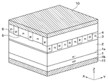
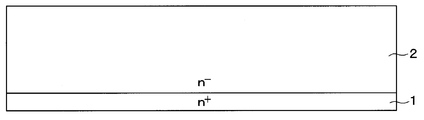
- n a top main surface 1a, on the main surface 1a of the opposite surface is a lower surface of the main surface 1a of the n + -type substrate 1 made of SiC to the back surface 1b - It forms using what formed the type
- the n + -type substrate 1 has an impurity concentration of, for example, about 1 ⁇ 10 18 to 5 ⁇ 10 18 cm ⁇ 3 .
- the n ⁇ -type layer 2 is composed of an epitaxial film of SiC having a dopant concentration lower than that of the n + -type substrate 1.
- the n ⁇ -type layer 2 has an impurity concentration of, for example, about 1 ⁇ 10 16 cm ⁇ 3 .
- a JBS structure including a PN diode in SBD is formed, and a breakdown voltage structure is formed in the outer peripheral region.
- a SiC semiconductor device is configured.
- n - surface side of the mold layer 2 on the opposite side i.e. the n + -type substrate 1, JFET 3 and the field block layer 4 composed of SiC is formed, n - -type Layer 2 is connected to JFET portion 3.
- the JFET portion 3 and the electric field blocking layer 4 constitute an electric field protective layer, and are formed only in the cell region. At least a part of the JFET portion 3 and the electric field blocking layer 4 are both extended in the X direction and arranged alternately repeatedly in the Y direction. That is, as shown in FIG. 2, when viewed from the direction normal to the main surface of the n + -type substrate 1, at least a portion field blocking layer 4 of JFET 3 is a plurality of strip-shaped, i.e. stripes The layouts are arranged alternately.
- the JFET portion 3 is formed to the lower side of the electric field blocking layer 4 so that the depth of the lower surface of the JFET portion 3 is deeper than the depth of the lower surface of the electric field blocking layer 4. There is. Therefore, the stripe-shaped portion of the JFET portion 3 is connected below the electric field blocking layer 4, but each of the stripe-shaped portions is between the plurality of electric field blocking layers 4. It has been placed.
- Each portion of the stripe-shaped portion of the JFET portion 3, that is, each strip-shaped portion, has a width of, for example, 0.5 ⁇ m.
- the thickness of the JFET portion 3 is, for example, 0.6 to 1.6 ⁇ m, here 1.0 ⁇ m, and the n-type impurity concentration is higher than that of the n ⁇ -type layer 2, for example, 1.0 It is said to be ⁇ 10 17 / cm 3 .
- the field blocking layer 4 is composed of a p-type impurity layer. As described above, the field blocking layer 4 is in the form of stripes, and each strip-like portion of the field blocking layer 4 in the form of stripes has a width of, for example, 0.5 ⁇ m and a thickness of, for example, 0.5 to 1 .5 ⁇ m, here 0.9 ⁇ m.
- the electric field blocking layer 4 has, for example, a p-type impurity concentration of 5.0 ⁇ 10 17 / cm 3 . In the case of the present embodiment, the electric field blocking layer 4 has a constant p-type impurity concentration in the depth direction. In the field blocking layer 4, the surface opposite to the n ⁇ -type layer 2 is flush with the surface of the JFET portion 3.
- an n-type current distribution layer 5 and a p-type connection layer 6 made of SiC are formed on the JFET portion 3 and the electric field blocking layer 4.
- the n-type current dispersion layer 5 and the p-type connection layer 6 are also formed only in the cell region.
- the n-type current dispersion layer 5 is a layer that allows the current flowing through the channel to diffuse in the Y direction as described later, and is connected to the JFET portion 3.
- the n-type current dispersion layer 5 has a higher n-type impurity concentration than the n ⁇ -type layer 2.
- the n-type impurity concentrations of the JFET portion 3 and the n-type current dispersion layer 5 are made equal.
- the n-type current dispersion layer 5 is formed in a strip shape by extending in the Y direction, and is formed in a stripe shape by arranging a plurality of them in the X direction.
- the width of the n-type current dispersion layer 5 which is the dimension in the X direction is arbitrary, but is wider than the width of the stripe-shaped portion of the JFET portion 3 and is 4 ⁇ m here.
- the thickness of the n-type current dispersion layer 5 is arbitrary, but is 0.5 ⁇ m here.
- the drift layer is divided into the n ⁇ -type layer 2, the JFET portion 3 and the n-type current dispersion layer 5 for the sake of convenience, they are both parts constituting the drift layer, and It is connected.
- the p-type connection layer 6 is provided to connect a Schottky electrode 10 described later and the electric field block layer 4.
- the p-type connection layer 6 has portions extending in a direction intersecting with the electric field blocking layer 4 and is formed to have intersections overlapping each other.
- a plurality of p-type connection layers 6 are formed in a stripe shape by extending in the Y direction.
- the p-type connection layer 6 has a thickness equal to or greater than that of the n-type current dispersion layer 5 so that the depth of the lower surface of the p-type connection layer 6 is deeper than the depth of the upper surface of the electric field block layer 4 And is connected to the electric field blocking layer 4. That is, a plurality of p-type connection layers 6 are formed to penetrate the n-type current distribution layer 5 from the surface of the n-type current distribution layer 5 to reach the electric field block layer 4.
- the n-type current dispersion layers 5 are arranged between the p-type connection layers 6 in the form of stripes.
- the distance between the plurality of p-type connection layers 6 corresponds to the width of the n-type current dispersion layer 5 described above, and is 4 ⁇ m here.
- the thickness of the p-type connection layer 6 may be any as long as it is equal to or more than the n-type current dispersion layer 5.
- the p-type connection layer 6 has a thickness of 0.6 ⁇ m.
- n - n-type current spreading layer 5 is not formed on the surface side of the mold layer 2, n to the surface of the SiC semiconductor substrate - has a type layer 2. That is, in the case of this embodiment, the n-type current dispersion layer 5 is formed only in the cell region, not in the outer peripheral region, and the n-type impurity concentration is low to the surface of the SiC semiconductor substrate. It has a structure.
- a p-type guard ring 8 is formed so as to surround the cell region.
- a plurality of p-type guard rings 8 are arranged concentrically, and are formed from the surface of the n ⁇ -type layer 2 and have the same depth as the electric field blocking layer 4 as shown in FIG.
- the p-type impurity concentration of the p-type guard ring 8 is arbitrary, in the case of this embodiment, the p-type guard ring 8 is formed with the same p-type impurity concentration as the electric field blocking layer 4 and the p-type connection layer 6. There is.
- an insulating film 9 made of, for example, a silicon oxide film or the like is formed so as to expose the cell region while covering the n ⁇ -type layer 2 and the p-type guard ring 8 in the outer peripheral region.
- An opening 9a is formed in the insulating film 9 at a position corresponding to the cell region, and the n-type current distribution layer 5 and the p-type connection layer 6 are exposed from the opening 9a.
- a Schottky electrode 10 is formed on the n-type current distribution layer 5, the p-type connection layer 6, and the insulating film 9, and the n-type current distribution layer 5 or p-type is formed. It is in contact with the connecting layer 6.
- the Schottky electrode 10 is in Schottky contact with the n-type current dispersion layer 5 and in contact with the p-type connection layer 6 so as not to be in an insulating state.
- the metal material of the Schottky electrode 10 any one or more of Ti, Al, AlSi, Mo, MoN, Ni, Au, and Pt can be used.
- Ti, Al, AlSi, Mo, or MoN which is a material having a low work function and capable of suppressing Vf as the metal material
- Ti, Al, AlSi, in particular, capable of lowering Vf. preferable an SBD is formed at the contact portion between Schottky electrode 10 and n-type current distribution layer 5.
- a PN diode comprising the p-type layer by the p-type connection layer 6 and the electric field block layer 4 and the n-type layer such as the JFET portion 3 or the n-type current dispersion layer 5 is configured. Be done.
- a back surface electrode 11 is formed on the back surface 1 b of the n + -type substrate 1.
- the back electrode 11 is in ohmic contact with the n + -type substrate 1 and is formed of a laminated structure of a plurality of metal layers such as Ti / Ni / Au or Ti / Ni / Au / Ag.
- the SiC semiconductor device provided with the SBD having the JBS structure is configured.
- the SiC semiconductor device provided with the SBD having such a JBS structure functions as an anode of the Schottky electrode 10 and a cathode of the back electrode 11.
- the electric field blocking layer 4 can suppress the rise of the electric field at the time of reverse bias as described above, the electric field applied to the interface between the Schottky electrode 10 and SiC can be relaxed, and the tunnel current flows in the Schottky barrier. Generation of leak current can be suppressed. Then, since the electric field can be relaxed by the electric field block layer 4, the n-type impurity concentration of the JFET portion 3 between the electric field block layers 4 can be made higher than that of the n ⁇ type layer 2.
- the n-type impurity concentration of JFET portion 3 is made equal to that of n - type layer 2
- the spread of the depletion layer from field block layer 4 to JFET portion 3 can be suppressed and the internal resistance Can be made smaller. Therefore, it is possible to suppress the decrease in the amount of current at the time of forward bias, and to suppress the increase in the on resistance Ron, and it is also possible to increase the slope of the rise of the current.
- the electric field block layer 4 can reduce the electric field, it is possible to suppress the leak current even if Vf is reduced by using a material having a lower work function as the material of the Schottky electrode 10.
- the Schottky electrode 10 is made of a material that can suppress Vf lower, the current can rise from a lower voltage at the time of forward bias, and the on resistance Ron can also be reduced.
- the electric field blocking layer 4 is formed at a deep position away from the Schottky electrode 10 and is connected to the Schottky electrode 10 via the p-type connection layer 6. Therefore, even if the electric field blocking layer 4 is formed at a deep position, it can be connected to the Schottky electrode 10 and can be set to the ground potential at the time of reverse bias. As a result, holes generated at the time of avalanche breakdown or the like can be extracted from the electric field blocking layer 4 through the p-type connection layer 6 from the Schottky electrode 10.
- the JFET portion 3 and the n-type current dispersion layer 5 are formed only in the cell region, and not formed in the outer peripheral region. For this reason, a high concentration n-type layer can be prevented from existing between the p-type guard rings 8, and the design and fabrication of the outer peripheral withstand voltage structure can be facilitated.
- the electric field block layer 4 is extended in the X direction
- the p-type connection layer 6 is extended in the Y direction, whereby the electric field block is viewed from the normal direction to the surface of the SiC semiconductor substrate.
- the layer 4 and the p-type connection layer 6 are orthogonal to each other.
- the electric field blocking layer 4 and the p-type connection layer 6 can be extended in the same direction, in this case, it is necessary to set the accuracy of the mask alignment at the time of forming them to, for example, 0.1 ⁇ m or less.
- the mask alignment accuracy can be relaxed to 0.1 ⁇ m or more. Therefore, the process of forming the electric field blocking layer 4 and the p-type connection layer 6 can be facilitated, and the mass productivity can be improved.
- the width of the JFET portion 3 is, for example, 1.0 ⁇ m
- the n-type impurity concentration is 1.0 ⁇ 10 17 / cm 3.
- the impurity concentration is set to y, as a value satisfying the following Formula 1 and Formula 2.
- Equation 1 The condition of (1) is expressed as Equation 1 described above.
- the width x of the JFET portion 3 As the width x of the JFET portion 3 is larger, the electric field applied to the interface between the Schottky electrode 10 and the n-type current dispersion layer 5 becomes larger even if the n-type impurity concentration y is lower. Further, as the n-type impurity concentration y of the JFET portion 3 is higher, the electric field applied to the interface between the Schottky electrode 10 and the n-type current dispersion layer 5 becomes larger even if the width x is smaller.
- the voltage BV capable of suppressing the leak current that is, the withstand voltage, was examined by changing the width x and the n-type impurity concentration y of the JFET portion 3 and the withstand voltage was calculated.
- the width x is 0.7 ⁇ m, for example, the withstand voltage may not be obtained depending on the n-type impurity concentration y.
- the width x and the n-type impurity concentration y at which a breakdown voltage of 1600 V can be obtained is plotted by this breakdown voltage calculation, it becomes as shown by the circle in FIG. 4C.
- an approximate curve connecting the plotted points that is, a pressure limit line, is expressed by Formula 1.
- the JFET resistance which is the resistance value of the JFET portion 3 decreases as the width x of the JFET portion 3 increases, and increases as the n-type impurity concentration y decreases.
- the larger the JFET resistance the higher the on-resistance.
- the change in the on-resistance was examined by changing the width x of the JFET portion 3 and the n-type impurity concentration y, and the result is shown in FIG. 4B.
- the n + -type substrate 1 is prepared, and the n ⁇ -type layer 2 is epitaxially grown on the main surface 1a.
- an epi substrate in which the n ⁇ -type layer 2 is formed in advance on the main surface 1 a of the n + -type substrate 1 may be used.
- the SiC semiconductor substrate of this embodiment is obtained.
- Step shown in FIG. 5B After arranging a mask (not shown), an area for forming JFET portion 3 and n-type current distribution layer 5 in the mask is opened. Then, ion implantation of an n-type impurity is performed on the mask to form the JFET portion 3 and the n-type current dispersion layer 5 in the surface layer portion of the n ⁇ -type layer 2. At this time, the n-type impurity concentration of the JFET portion 3 and that of the n-type current dispersion layer 5 can be made different, but are the same here. After that, the mask used in ion implantation is removed.
- Step shown in FIG. 5C After arranging a mask (not shown), an area for forming the field blocking layer 4 and the p-type guard ring 8 in the mask is opened. Then, by performing ion implantation of p-type impurities from the mask, thereby forming an electric field blocking layer 4 in the JFET portion 3, n - n in the surface of the mold layer 2 - apart from the type layer 2 of the surface position Form the lower part of the p-type guard ring 8.
- the mask which is not shown in figure is arrange
- p-type impurities are ion-implanted from above the mask to form the p-type connection layer 6 in the n-type current distribution layer 5 and at the surface of the n ⁇ -type layer 2 above the p-type guard ring 8. Form a part.
- the p-type connection layer 6 and the field blocking layer 4 overlap each other, and are connected at their intersections.
- the electric field blocking layer 4 and the p-type connection layer 6 are formed by ion implantation. For this reason, concentration variation and thickness variation can be reduced compared to the case of forming at least a part of these by epitaxial growth. Therefore, the design of these formation processes can be facilitated.
- the p-type guard ring 8 is formed simultaneously with the electric field blocking layer 4 and the p-type connection layer 6 here, the p-type guard ring 8 may be formed as a process separate from these.
- An insulating film 9 composed of a silicon oxide film or the like is formed on the surface of the n ⁇ -type layer 2 including the surfaces of the n-type current dispersion layer 5, the p-type connection layer 6 and the p-type guard ring 8. Then, the opening 9 a is formed in the insulating film 9 by performing photo-etching using a mask (not shown).
- a metal material for forming the Schottky electrode 10 is formed on the surface of the insulating film 9 including the inside of the opening 9a, and then the Schottky electrode 10 is formed by patterning. Form. Then, on the side of the back surface 1 b of the n + -type substrate 1, a metal material forming the back electrode 11 is deposited. Thereby, the SiC semiconductor device shown in FIGS. 1 to 3 is completed.
- the present embodiment is the same as the first embodiment except that the configuration and the like of the n-type current dispersion layer 5 are modified with respect to the first embodiment, and only the parts different from the first embodiment are different. explain.
- n - from the surface of the mold layer 2 forms a JFET portion 3 and the field block layer 4, n includes a JFET portion 3 and the electric field blocking layer 4 - -type layer 2
- the n-type current dispersion layer 5 and the p-type connection layer 6 are formed on the surface.
- an n-type layer 7 corresponding to the same SiC layer as the n-type current dispersion layer 5 is formed, and the p-type guard ring 8 penetrates the n-type layer 7 to form n ⁇ -type. It reaches the surface of the layer 2 and is formed to the same depth as the field blocking layer 4.
- the n-type layer 7 is formed by epitaxial growth simultaneously with the n-type current dispersion layer 5 and has the same n-type impurity concentration and thickness as the n-type current dispersion layer 5.
- the upper portions of the p-type connection layer 6 and the p-type guard ring 8 are formed by ion implantation of p-type impurities into the n-type current distribution layer 5 and the n-type layer 7.
- a mask (not shown) is disposed on the surface of the n ⁇ -type layer 2 to open an area for forming the JFET portion 3 in the mask. Then, ion implantation of an n-type impurity is performed on the mask to form the JFET portion 3 in the surface layer portion of the n ⁇ -type layer 2. After that, the mask is removed.
- Step shown in FIG. 7B After arranging a mask (not shown), an area for forming the field blocking layer 4 and the p-type guard ring 8 in the mask is opened. Then, ion implantation of p-type impurities is performed on the mask to form the electric field block layer 4 in the JFET portion 3 and to form the lower portion of the p-type guard ring 8 in the surface layer portion of the n ⁇ -type layer 2. . After that, the mask is removed.
- An epitaxial film 20 is formed.
- Step shown in FIG. 7D After arranging a mask (not shown), an area for forming p-type connection layer 6 and p-type guard ring 8 in the mask is opened. Then, ion implantation of p-type impurities is performed on the mask to form upper portions of the p-type connection layer 6 and the p-type guard ring 8 with respect to the n-type epitaxial film 20. As a result, the p-type connection layer 6 and the field blocking layer 4 overlap and become connected at these intersections, and the upper portion and the lower portion of the p-type guard ring 8 overlap and are connected to each other.
- the guard ring 8 is configured. Furthermore, the n-type current diffusion layer 5 is formed by the portion located in the cell region of the n-type epitaxial film 20, and the n-type layer 7 is formed by the portion located in the outer peripheral region.
- the SiC semiconductor device of the present embodiment is completed by performing the step shown in FIG. 5D described in the first embodiment and the subsequent steps.
- the top surface layout of the electric field block layer 4 is in the form of stripes, but the layout is not limited to stripes, and may be other layouts.
- the electric field blocking layer 4 may be laid out in a lattice or concentric manner, for example, concentrically, or in a dot manner.
- the electric field block layers 4 may be disposed on both sides of the JFET portion 3 in one direction parallel to the main surface 1a, and the electric field block layer 4 may be configured to suppress the rise of the electric field to the JFET portion 3 .
- the electric field block layer 4 since it is necessary to connect the p-type connection layer 6 to each of the separated electric field block layers 4, if the electric field block layer 4 is linearly formed like a stripe or the like. preferable.
- the upper surface layout of the p-type connection layer 6 is a stripe, it may be another layout.
- the upper surface layout of the p-type connection layer 6 may be lattice-like, and the lattice-like p-type connection layer 6 may be connected to each electric field block layer 4. In that case, lines in one direction arranged in parallel among the p-type connection layers 6 formed in a lattice form extend in a direction intersecting the extending direction of the electric field block layer 4 in the case where the upper surface layout is formed in stripes. It should be made to be a part that
- the n-type impurity concentration of the JFET portion 3 and the n-type current dispersion layer 5 are the same, but may be different.
- the n-type impurity concentration of the JFET portion 3 may be different from that of the n-type current dispersion layer 5 so that the n-type impurity concentration of the JFET portion 3 is higher than that of the n-type current dispersion layer 5.
- the p-type guard ring 8 has been described as an example of the p-type layer forming the breakdown voltage structure formed in the outer peripheral region so as to surround the cell region.
- a resurf layer can also be provided.
- an SBD having a Schottky barrier with respect to n-type SiC is taken as an example, and a SiC semiconductor device in which the first conductivity type is n-type and the second conductivity type is p-type is described. .
- this is merely an example, and the present disclosure is also applied to a SiC semiconductor device in which the conductivity type of each part is reversed and the first conductivity type is p-type and the second conductivity type is n-type. can do.
Landscapes
- Electrodes Of Semiconductors (AREA)
Applications Claiming Priority (2)
| Application Number | Priority Date | Filing Date | Title |
|---|---|---|---|
| JP2017-197996 | 2017-10-11 | ||
| JP2017197996A JP7098906B2 (ja) | 2017-10-11 | 2017-10-11 | ショットキーバリアダイオードを備えた炭化珪素半導体装置およびその製造方法 |
Publications (1)
| Publication Number | Publication Date |
|---|---|
| WO2019073776A1 true WO2019073776A1 (ja) | 2019-04-18 |
Family
ID=66100582
Family Applications (1)
| Application Number | Title | Priority Date | Filing Date |
|---|---|---|---|
| PCT/JP2018/034871 Ceased WO2019073776A1 (ja) | 2017-10-11 | 2018-09-20 | ショットキーバリアダイオードを備えた炭化珪素半導体装置およびその製造方法 |
Country Status (2)
| Country | Link |
|---|---|
| JP (1) | JP7098906B2 (https=) |
| WO (1) | WO2019073776A1 (https=) |
Cited By (5)
| Publication number | Priority date | Publication date | Assignee | Title |
|---|---|---|---|---|
| US11031472B2 (en) | 2018-12-28 | 2021-06-08 | General Electric Company | Systems and methods for integrated diode field-effect transistor semiconductor devices |
| CN112993017A (zh) * | 2021-02-23 | 2021-06-18 | 厦门市三安集成电路有限公司 | 碳化硅器件外延结构及其制备方法 |
| CN115485859A (zh) * | 2020-05-06 | 2022-12-16 | 电导魔方股份有限公司 | 具有增强紧固性的碳化硅结势垒肖特基二极管 |
| US20230290887A1 (en) * | 2020-09-24 | 2023-09-14 | Rohm Co., Ltd. | Semiconductor device |
| EP4340032A1 (en) * | 2022-09-15 | 2024-03-20 | Nexperia B.V. | Semiconductor power device with improved ruggedness |
Families Citing this family (4)
| Publication number | Priority date | Publication date | Assignee | Title |
|---|---|---|---|---|
| JP7585646B2 (ja) | 2019-08-13 | 2024-11-19 | 富士電機株式会社 | 半導体装置および半導体装置の製造方法 |
| JP7647239B2 (ja) | 2021-03-30 | 2025-03-18 | 富士電機株式会社 | 半導体装置 |
| JP2022159760A (ja) * | 2021-04-05 | 2022-10-18 | ローム株式会社 | 半導体装置 |
| JP2025012573A (ja) * | 2023-07-13 | 2025-01-24 | 株式会社東芝 | 半導体装置 |
Citations (10)
| Publication number | Priority date | Publication date | Assignee | Title |
|---|---|---|---|---|
| JPH11330498A (ja) * | 1998-05-07 | 1999-11-30 | Fuji Electric Co Ltd | ショットキーバリアダイオードおよびその製造方法 |
| JP2002076370A (ja) * | 2000-09-05 | 2002-03-15 | Fuji Electric Co Ltd | 超接合ショットキーダイオード |
| JP2004022796A (ja) * | 2002-06-17 | 2004-01-22 | Matsushita Electric Ind Co Ltd | 炭化珪素半導体素子およびその形成方法 |
| JP2007081448A (ja) * | 2006-12-25 | 2007-03-29 | Fuji Electric Device Technology Co Ltd | 超接合半導体素子 |
| US20110037139A1 (en) * | 2008-03-21 | 2011-02-17 | Microsemi Corporation | Schottky barrier diode (sbd) and its off-shoot merged pn/schottky diode or junction barrier schottky (jbs) diode |
| WO2013183677A1 (ja) * | 2012-06-06 | 2013-12-12 | ローム株式会社 | 半導体装置およびその製造方法 |
| JP2014060376A (ja) * | 2012-09-14 | 2014-04-03 | Hyundai Motor Company Co Ltd | ショットキーバリアダイオードおよびその製造方法 |
| JP2014060276A (ja) * | 2012-09-18 | 2014-04-03 | Denso Corp | 炭化珪素半導体装置 |
| JP2015216200A (ja) * | 2014-05-09 | 2015-12-03 | 株式会社豊田中央研究所 | 半導体装置 |
| US20160380059A1 (en) * | 2015-06-26 | 2016-12-29 | General Electric Company | Active area designs for silicon carbide super-junction power devices |
-
2017
- 2017-10-11 JP JP2017197996A patent/JP7098906B2/ja active Active
-
2018
- 2018-09-20 WO PCT/JP2018/034871 patent/WO2019073776A1/ja not_active Ceased
Patent Citations (10)
| Publication number | Priority date | Publication date | Assignee | Title |
|---|---|---|---|---|
| JPH11330498A (ja) * | 1998-05-07 | 1999-11-30 | Fuji Electric Co Ltd | ショットキーバリアダイオードおよびその製造方法 |
| JP2002076370A (ja) * | 2000-09-05 | 2002-03-15 | Fuji Electric Co Ltd | 超接合ショットキーダイオード |
| JP2004022796A (ja) * | 2002-06-17 | 2004-01-22 | Matsushita Electric Ind Co Ltd | 炭化珪素半導体素子およびその形成方法 |
| JP2007081448A (ja) * | 2006-12-25 | 2007-03-29 | Fuji Electric Device Technology Co Ltd | 超接合半導体素子 |
| US20110037139A1 (en) * | 2008-03-21 | 2011-02-17 | Microsemi Corporation | Schottky barrier diode (sbd) and its off-shoot merged pn/schottky diode or junction barrier schottky (jbs) diode |
| WO2013183677A1 (ja) * | 2012-06-06 | 2013-12-12 | ローム株式会社 | 半導体装置およびその製造方法 |
| JP2014060376A (ja) * | 2012-09-14 | 2014-04-03 | Hyundai Motor Company Co Ltd | ショットキーバリアダイオードおよびその製造方法 |
| JP2014060276A (ja) * | 2012-09-18 | 2014-04-03 | Denso Corp | 炭化珪素半導体装置 |
| JP2015216200A (ja) * | 2014-05-09 | 2015-12-03 | 株式会社豊田中央研究所 | 半導体装置 |
| US20160380059A1 (en) * | 2015-06-26 | 2016-12-29 | General Electric Company | Active area designs for silicon carbide super-junction power devices |
Cited By (6)
| Publication number | Priority date | Publication date | Assignee | Title |
|---|---|---|---|---|
| US11031472B2 (en) | 2018-12-28 | 2021-06-08 | General Electric Company | Systems and methods for integrated diode field-effect transistor semiconductor devices |
| CN115485859A (zh) * | 2020-05-06 | 2022-12-16 | 电导魔方股份有限公司 | 具有增强紧固性的碳化硅结势垒肖特基二极管 |
| US20230290887A1 (en) * | 2020-09-24 | 2023-09-14 | Rohm Co., Ltd. | Semiconductor device |
| CN112993017A (zh) * | 2021-02-23 | 2021-06-18 | 厦门市三安集成电路有限公司 | 碳化硅器件外延结构及其制备方法 |
| CN112993017B (zh) * | 2021-02-23 | 2022-08-09 | 厦门市三安集成电路有限公司 | 碳化硅器件外延结构及其制备方法 |
| EP4340032A1 (en) * | 2022-09-15 | 2024-03-20 | Nexperia B.V. | Semiconductor power device with improved ruggedness |
Also Published As
| Publication number | Publication date |
|---|---|
| JP2019071394A (ja) | 2019-05-09 |
| JP7098906B2 (ja) | 2022-07-12 |
Similar Documents
| Publication | Publication Date | Title |
|---|---|---|
| WO2019073776A1 (ja) | ショットキーバリアダイオードを備えた炭化珪素半導体装置およびその製造方法 | |
| US10964809B2 (en) | Semiconductor device and manufacturing process therefor | |
| US10522673B2 (en) | Semiconductor device having a schottky barrier diode | |
| JP5198030B2 (ja) | 半導体素子 | |
| WO2019044921A1 (ja) | 炭化珪素半導体装置およびその製造方法 | |
| US20180197983A1 (en) | Semiconductor device and method of manufacturing semiconductor device | |
| US11139376B2 (en) | Silicon carbide semiconductor device and method of manufacturing silicon carbide semiconductor device | |
| JP5774205B2 (ja) | 半導体装置 | |
| JP2006269720A (ja) | 半導体素子及びその製造方法 | |
| JP2006005275A (ja) | 電力用半導体素子 | |
| US10714611B2 (en) | Silicon carbide semiconductor device | |
| JP2008016461A (ja) | 半導体装置 | |
| WO2019054517A1 (ja) | 半導体装置およびその製造方法 | |
| WO2020121371A1 (ja) | 炭化珪素半導体装置およびその製造方法 | |
| KR101438620B1 (ko) | 쇼트키 배리어 다이오드 및 그 제조 방법 | |
| US10840386B2 (en) | Semiconductor apparatus | |
| JP2007281034A (ja) | 電力用半導体素子 | |
| JP2020136493A (ja) | 半導体装置 | |
| US12432989B2 (en) | Semiconductor device and method for manufacturing the same | |
| JP7078226B2 (ja) | 半導体装置 | |
| JPWO2014155472A1 (ja) | 半導体素子 | |
| JP2004335697A (ja) | 接合型電界効果トランジスタ、その製造方法および半導体装置 | |
| JP2022182509A (ja) | 半導体装置およびその製造方法 | |
| JP2009043924A (ja) | ダイオード | |
| JP2019165166A (ja) | 炭化珪素半導体装置およびその製造方法 |
Legal Events
| Date | Code | Title | Description |
|---|---|---|---|
| 121 | Ep: the epo has been informed by wipo that ep was designated in this application |
Ref document number: 18867183 Country of ref document: EP Kind code of ref document: A1 |
|
| NENP | Non-entry into the national phase |
Ref country code: DE |
|
| 122 | Ep: pct application non-entry in european phase |
Ref document number: 18867183 Country of ref document: EP Kind code of ref document: A1 |