WO2019064744A1 - 表示装置 - Google Patents
表示装置 Download PDFInfo
- Publication number
- WO2019064744A1 WO2019064744A1 PCT/JP2018/023622 JP2018023622W WO2019064744A1 WO 2019064744 A1 WO2019064744 A1 WO 2019064744A1 JP 2018023622 W JP2018023622 W JP 2018023622W WO 2019064744 A1 WO2019064744 A1 WO 2019064744A1
- Authority
- WO
- WIPO (PCT)
- Prior art keywords
- insulating layer
- transistor
- layer
- display device
- semiconductor layer
- Prior art date
- Legal status (The legal status is an assumption and is not a legal conclusion. Google has not performed a legal analysis and makes no representation as to the accuracy of the status listed.)
- Ceased
Links
Images




Classifications
-
- G—PHYSICS
- G09—EDUCATION; CRYPTOGRAPHY; DISPLAY; ADVERTISING; SEALS
- G09F—DISPLAYING; ADVERTISING; SIGNS; LABELS OR NAME-PLATES; SEALS
- G09F9/00—Indicating arrangements for variable information in which the information is built-up on a support by selection or combination of individual elements
- G09F9/30—Indicating arrangements for variable information in which the information is built-up on a support by selection or combination of individual elements in which the desired character or characters are formed by combining individual elements
-
- H—ELECTRICITY
- H05—ELECTRIC TECHNIQUES NOT OTHERWISE PROVIDED FOR
- H05B—ELECTRIC HEATING; ELECTRIC LIGHT SOURCES NOT OTHERWISE PROVIDED FOR; CIRCUIT ARRANGEMENTS FOR ELECTRIC LIGHT SOURCES, IN GENERAL
- H05B33/00—Electroluminescent light sources
- H05B33/02—Details
-
- H—ELECTRICITY
- H10—SEMICONDUCTOR DEVICES; ELECTRIC SOLID-STATE DEVICES NOT OTHERWISE PROVIDED FOR
- H10D—INORGANIC ELECTRIC SEMICONDUCTOR DEVICES
- H10D30/00—Field-effect transistors [FET]
- H10D30/60—Insulated-gate field-effect transistors [IGFET]
- H10D30/67—Thin-film transistors [TFT]
-
- H—ELECTRICITY
- H10—SEMICONDUCTOR DEVICES; ELECTRIC SOLID-STATE DEVICES NOT OTHERWISE PROVIDED FOR
- H10K—ORGANIC ELECTRIC SOLID-STATE DEVICES
- H10K59/00—Integrated devices, or assemblies of multiple devices, comprising at least one organic light-emitting element covered by group H10K50/00
- H10K59/10—OLED displays
- H10K59/12—Active-matrix OLED [AMOLED] displays
Definitions
- the present invention relates to a display device.
- the present invention relates to a display device using a silicon-based semiconductor and an oxide semiconductor.
- Low temperature poly-silicon is widely used in liquid crystal display devices and organic EL display devices because it has high on-state driving ability and high carrier mobility.
- Low temperature polycrystalline silicon is formed by irradiating amorphous silicon with a laser.
- Patent Document 1 discloses a display device provided with a transistor using an oxide semiconductor layer.
- the drivability in the on state and the carrier mobility do not reach that of the polycrystalline silicon layer.
- an object of the present invention is to provide a display device provided with a plurality of types of transistors each having a different semiconductor layer.
- a display device includes a substrate having a display region, and a plurality of pixels arranged in the display region of the substrate, each of the plurality of pixels being a light emitting element, a first transistor, a first
- the transistor includes a second transistor, a first insulating layer, and a second insulating layer, the first transistor includes a silicon layer, and the second transistor includes an oxide semiconductor layer disposed above the first insulating layer.
- the first insulating layer includes a silicon oxide layer, and the first insulating layer is disposed between the silicon layer and the oxide semiconductor layer over the display region in common to the plurality of pixels.
- the layer comprises diamond like carbon, and the second insulating layer is disposed between the channel region of the second transistor and the first insulating layer.
- FIG. 1 is a schematic view showing a display area 103 of a display device 100 according to the present embodiment, and is a schematic view when the display area 103 is viewed in plan.
- a state in which the display device 100 is viewed from the direction perpendicular to the screen is referred to as “plan view”.
- the display device 100 includes a display area 103 formed on an insulating surface, a scanning line drive circuit 104, and a driver IC 106.
- the insulating surface is the surface of the substrate 101.
- a flexible substrate polyimide, polyethylene terephthalate, polyethylene naphthalate, triacetyl cellulose, cyclic olefin copolymer, cycloolefin polymer, or other flexible resin substrate
- the substrate 101 is preferably a material that transmits light.
- a substrate similar to the substrate 101 can be used. Note that in the case where the display device does not need to be bent, a metal substrate, a ceramic substrate, a semiconductor substrate, or the like may be used as the substrate 101.
- each of the plurality of pixels 109 includes a pixel circuit including at least a selection transistor, a driving transistor, and a light emitting element.
- a peripheral area 110 surrounds the periphery of the display area 103.
- the driver IC 106 functions as a control unit that supplies a signal to the scan line drive circuit 104. Then, a signal line drive circuit is incorporated in the driver IC 106.
- FIG. 1 shows an example in which the driver IC 106 is provided on the substrate 101, the driver IC 106 may be provided on the flexible printed substrate 108 and externally attached. Flexible printed circuit board 108 is connected to terminal 107 provided in peripheral region 110.
- the display area 103 is provided with a plurality of scanning lines 111 provided along the first direction, and a plurality of signal lines 112 provided along the second direction intersecting the first direction.
- pixels 109 connected to the scanning lines 111 and the signal lines 112 are arranged in a matrix.
- the pixel 109 includes a light emitting element including a part of the pixel electrode (anode), an organic layer (light emitting portion) including a light emitting layer stacked on the pixel electrode, and a cathode (cathode).
- a data signal corresponding to image data is given to each pixel 109 from the signal line driver circuit via the signal line 112.
- a transistor electrically connected to a pixel electrode provided in each pixel 109 can be driven in accordance with the data signal, and screen display can be performed according to image data.
- a thin film transistor (TFT) can be used.
- a sealing film in which an inorganic insulating layer and an organic insulating layer are stacked may be provided over the light emitting element.
- the counter substrate 102 is provided over the light-emitting element through an adhesive.
- a polarizing plate and a retardation plate are provided on the counter substrate 102. The polarizing plate and the retardation plate are provided in order to suppress deterioration of visibility due to reflection of external light incident on the display device 100 by the pixel electrode. Note that in the case of providing a polarizing plate and a retardation plate over a light emitting element (or a sealing film) via an adhesive, the counter substrate 102 may not necessarily be provided.
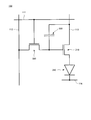
- FIG. 2 shows a pixel circuit included in each of the plurality of pixels 109 of the display device 100 according to the present embodiment.
- Each of the plurality of pixels 109 includes at least a transistor 210, a transistor 220, a storage capacitor 230, and a light emitting element 240.
- the transistor 210 functions as a drive transistor. That is, they are transistors which are connected to the light emitting element 240 and control the light emission luminance of the light emitting element 240.
- the gate of the transistor 210 is connected to the transistor 220, the source is connected to the driving power supply line 113, and the drain is connected to the anode of the light emitting element 240.
- the drain current of the transistor 210 is controlled by the gate-source voltage.
- the storage capacitor 230 is connected between the gate and the source of the transistor 210 so as to maintain the gate-source voltage.
- the transistor 220 functions as a selection transistor. That is, the transistor 220 controls conduction between the signal line 112 and the gate of the transistor 210.
- the transistor 220 has a gate connected to the scan line 111, a source connected to the signal line 112, and a drain connected to the gate of the transistor 210.
- the light emitting element 240 has an anode connected to the drain of the transistor 210 and a cathode connected to the reference power supply line 114.
- the transistor 210 operates in a saturated state because it functions as a driving transistor. Therefore, it is preferable to have high driving ability in the on state, and it is desirable to have high carrier mobility.
- the transistor 220 functions as a selection transistor, it is preferable that the transistor 220 have favorable switching characteristics. That is, it is preferable that the current value in the on state is large and the current value in the off state is small.
- the transistor 210 and the transistor 220 have different required characteristics.
- different semiconductor materials are used in the transistor 210 and the transistor 220.
- the transistor 210 is a transistor in which a channel is formed in a silicon layer such as amorphous silicon or polycrystalline silicon
- the transistor 220 is a transistor in which a channel is formed in an oxide semiconductor layer.
- a transistor using a polycrystalline silicon layer In the manufacture of a transistor using a polycrystalline silicon layer, it is known that the characteristic variation of the transistor is alleviated and the characteristic of the transistor is improved by hydrogenating the polycrystalline silicon layer.
- manufacturing of a transistor using an oxide semiconductor layer has the following problems. For example, when hydrogen or moisture intrudes from the layer adjacent to the oxide semiconductor layer into the oxide semiconductor layer, the characteristics of the transistor are degraded. Specifically, a decrease in carrier mobility, threshold variation and the like occur.
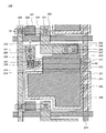
- FIG. 3 is a plan view illustrating the configuration of the pixel 109 included in the display device 100 according to the present embodiment.
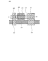
- FIG. 4 is an enlarged plan view illustrating the configuration of a part of the pixel 109 included in the display device 100 according to the present embodiment.
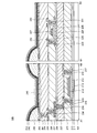
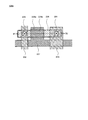
- FIG. 5 shows a cross-sectional view taken along line A1-A2 of FIG. 3 and a cross-sectional view taken along line B1-B2 of FIG. Note that in FIG. 5, a cross-sectional view of a transistor 210 using polycrystalline silicon is shown between A1 and A2, and a cross-sectional view of a transistor 220 using an oxide semiconductor layer is shown between B1 and B2.
- a base film 211 is provided on the substrate 101.
- a glass substrate, a quartz substrate, a flexible substrate (polyimide, polyethylene terephthalate, polyethylene naphthalate, triacetyl cellulose, cyclic olefin copolymer, cycloolefin polymer, or other flexible resin substrate) is used as the substrate 101.
- a flexible substrate polyimide, polyethylene terephthalate, polyethylene naphthalate, triacetyl cellulose, cyclic olefin copolymer, cycloolefin polymer, or other flexible resin substrate
- the base film 211 is an insulating layer formed of an inorganic insulating material such as silicon oxide, silicon nitride, or aluminum oxide.
- the base film 211 is not limited to a single layer, and may have a stacked structure in which a silicon oxide layer and a silicon nitride layer are combined, for example. This structure may be appropriately determined in consideration of the adhesion to the substrate 101 and the gas barrier property to the transistor 220 described later.
- the transistor 210 is provided over the base film 211.
- the transistor 210 functions as a drive transistor.
- the transistor 210 includes a semiconductor layer 212, a gate insulating film 213 provided over the semiconductor layer 212, and a gate electrode 214 provided over the gate insulating film 213.
- the transistor 210 is a transistor using polycrystalline silicon as the semiconductor layer 212, which has high drivability in the on state and high carrier mobility.
- As the gate insulating film 213, a silicon oxide film, a silicon nitride film, or the like can be used.
- As the gate electrode 214 a metal material such as copper, molybdenum, tantalum, tungsten, or aluminum, or an alloy material of these can be used.
- an interlayer insulating layer 215 which covers the gate electrode 214 is provided over the transistor 210.
- Contact holes 216 and 217 are provided in the interlayer insulating film 215 and the gate insulating film 213.
- Source and drain electrodes 218 and 219 are provided over the interlayer insulating layer 215.
- the source and drain electrodes 218 and 219 are connected to the semiconductor layer 212 through the contact holes 216 and 217.
- the interlayer insulating layer 215 silicon oxide or silicon nitride can be used.
- the interlayer insulating layer 215 may be a single layer or a stacked layer.
- a metal material such as copper, titanium, molybdenum, or aluminum, or an alloy material of these can be used.
- the conductive layer including the source or drain electrode 219 corresponds to the driving power supply line 113 shown in FIG.
- the semiconductor layer 221 is further provided over the base film 211 which is the same as the semiconductor layer 212.
- the semiconductor layer 221, the gate insulating film 213, and the gate electrode 214 form a storage capacitor 230.
- the semiconductor layer 221 is connected to the source or drain electrode 219 through a contact hole 222 provided in the gate insulating film 213 and the interlayer insulating layer 215.
- An interlayer insulating layer 223 is provided over the interlayer insulating layer 215 and the source and drain electrodes 218 and 219.
- the interlayer insulating layer 223 can be made of silicon oxide or silicon nitride.
- Silicon nitride contains hydrogen at a relatively high concentration, and is a film that easily releases hydrogen.
- hydrogen can be supplied to the semiconductor layer 212 which is polycrystalline silicon.
- hydrogen bonds can terminate the dangling bonds (also referred to as dangling bonds) present at the interface and the inside of polycrystalline silicon.
- the energy level density in the energy gap is reduced, so that the characteristics of the transistor 210 can be improved.
- Silicon oxide is provided to suppress diffusion of hydrogen contained in silicon nitride provided thereunder to the outside. That is, in order to prevent entry of hydrogen into a semiconductor layer which is an oxide semiconductor provided in a layer higher than the interlayer insulating layer 223, hydrogen is provided.
- the transistor 220 is provided over the interlayer insulating layer 223.
- the transistor 220 functions as a selection transistor.
- the transistor 220 includes a semiconductor layer 225, a gate insulating film 226 provided over the semiconductor layer 225, and a gate electrode 227 provided over the gate insulating film 226.
- the transistor 220 is a transistor in which an oxide semiconductor is used as the semiconductor layer 225, which has a large current value in the on state and a small current value in the off state, and has favorable switching characteristics.
- a gate electrode 227 is provided over the gate insulating film 226, a gate electrode 227 is provided.
- the gate electrode 227 a metal material such as copper, molybdenum, tantalum, tungsten, or aluminum, or an alloy material of these can be used.
- FIG. 5 shows the case where the transistor 220 has a top gate structure, the transistor 220 may have a bottom gate structure.
- the transistor 220 using an oxide semiconductor layer as the semiconductor layer 225 when hydrogen intrudes into the semiconductor layer 225, the threshold variation of the transistor 220 is increased, and carrier characteristics may be degraded, such as carrier mobility may be degraded. In particular, in the channel region of the transistor 220, the transistor characteristics are greatly affected.
- an insulating layer 224 for preventing entry of hydrogen into the channel region is provided in a region overlapping with the channel region of the transistor 220. It is preferable that the insulating layer 224 be a material which has a low concentration of hydrogen and does not transmit hydrogen as much as possible.
- the insulating layer 224 for example, diamond like carbon is preferably used.
- diamond-like carbon refers to an amorphous hard film mainly composed of a hydrocarbon or an allotrope of carbon.
- diamond-like carbon has a structure in which both a diamond bond (SP 3 bond) and a graphite bond (SP 2 bond) are mixed.
- Diamond-like carbon can be deposited to a thickness of 50 nm or more and 100 nm or less by a CVD method. Since diamond like carbon is a dense film, it can suppress the permeation of hydrogen. Thus, the interlayer insulating layer 223 does not need to be thick, so that the thickness of the interlayer insulating layer 223 can be reduced. In addition, since diamond like carbon is formed into a film by a CVD method, for example, generated dust can be reduced as compared with the case of forming an aluminum oxide film by a sputtering method. Furthermore, diamond-like carbon formed into a film by CVD method is excellent in film thickness uniformity compared with aluminum oxide formed into a film by sputtering method.
- the insulating layer 224 can be formed by processing the diamond-like carbon into an island shape by an etching method. After that, an oxide semiconductor may be formed over the interlayer insulating layer 223 to form an island-shaped semiconductor layer 225.
- the insulating layer 224 is provided to overlap with at least a region overlapping with the channel region of the transistor 220. That is, the gate electrode 227 of the transistor 220 and the insulating layer 224 are provided so as to overlap with each other.
- the hydrogen concentration contained in the insulating layer 224 is preferably lower than the hydrogen concentration contained in the interlayer insulating layer 223.
- hydrogen released from the interlayer insulating layer 223 is formed in the semiconductor layer 225 by providing the insulating layer 224 which contains low concentration of hydrogen and does not transmit hydrogen as much as possible in a region overlapping with the channel region of the transistor 220. It is possible to suppress intrusion. Accordingly, deterioration of transistor characteristics such as an increase in threshold variation of the transistor 220 and a decrease in carrier mobility can be suppressed.
- the insulating layer 224 is preferably provided in contact with the semiconductor layer 225.
- entry of hydrogen from the lower surface of the semiconductor layer 225 can be suppressed.
- an interlayer insulating layer 228 which covers the gate electrode 227 is provided over the transistor 220.
- Contact holes 229 and 231 are provided in the interlayer insulating layer 228 and the gate insulating film 226.
- Source and drain electrodes 232 and 233 are provided over the interlayer insulating layer 228.
- the source and drain electrodes 232 and 233 are connected to the semiconductor layer 225 through the contact holes 229 and 231.
- the interlayer insulating layer 228 silicon oxide or silicon nitride can be used.
- the interlayer insulating layer 228 may be a single layer or a stacked layer. In this case, it is preferable that silicon oxide or silicon nitride be deposited under conditions which do not contain hydrogen.
- a metal material such as copper, titanium, molybdenum, or aluminum, or an alloy material of these can be used.
- the source or drain electrode 233 is connected to the conductive layer 247 through the contact hole 245, and the conductive layer 247 is connected to the gate of the transistor 210 through the contact hole 248. It is connected to the electrode 214.
- the contact hole 245 is provided in the interlayer insulating layer 228, and the contact hole 248 is provided in the gate insulating film 226, the interlayer insulating layer 223, and the interlayer insulating layer 115.
- the conductive layer 247 is formed in the same step as the gate electrode 227 of the transistor 220.
- the conductive layer including the gate electrode 227 corresponds to the scanning line 111 shown in FIG. 2, and the conductive layer including the source or drain electrode 232 corresponds to the signal line 112 shown in FIG.
- a planarization film 234 is provided over the interlayer insulating layer 228 and the source and drain electrodes 232 and 233.
- the planarization film 234 is provided to planarize unevenness due to various transistors, wirings, and the like disposed in the lower layer.
- an organic insulating material such as an acrylic resin or a polyimide resin can be used.
- a light emitting element 240 is provided on the planarization film 234.
- the light emitting element 240 at least includes a pixel electrode 235 (also referred to as an anode), an organic layer 242 including a light emitting layer stacked on the pixel electrode, and a cathode 243 (also referred to as a cathode).
- the pixel electrode 235 is electrically connected to the source electrode or drain electrode 218.
- the source or drain electrode 218 is connected to the conductive layer 237 provided over the gate insulating film 226 through the contact hole 236 provided in the interlayer insulating film 223 and the gate insulating film 226.
- the conductive layer 237 is connected to a conductive layer 239 provided over the interlayer insulating layer 228 via a contact hole 238 provided in the interlayer insulating layer 228.
- the conductive layer 239 is connected to the pixel electrode 235 provided on the planarization film 234 through a contact hole 241 provided in the planarization film 234.
- the conductive layer 237 is a layer formed in the same step as the gate electrode 227 of the transistor 220.
- the conductive layer 239 is a layer formed in the same step as the source and drain electrodes 232 and 233.
- the pixel electrode 235 is disposed for each of the plurality of pixels 109.
- a material of the pixel electrode 235 in order to reflect the light generated in the organic layer 242 to the cathode 243 side, it is preferable to include a metal layer having high reflectance.
- silver (Ag) can be used as the metal layer with high reflectance.
- a transparent conductive layer may be laminated.
- ITO titanium oxide-doped indium oxide
- IZO indium oxide / zinc oxide
- the pixel electrode 235 may be configured by laminating a metal layer having high reflectance and a transparent conductive layer.
- An insulating layer 244 is provided between two adjacent pixels 109.
- the insulating layer 244 is provided to cover the peripheral portion of the pixel electrode 235.
- the insulating layer 244 is provided to cover a connection region between the conductive layer 239 and the pixel electrode 235.
- an inorganic insulating material or an organic insulating material can be used as a material of the insulating layer 244.
- an inorganic insulating material for example, silicon oxide, silicon nitride, or a combination thereof can be used.
- an organic insulating material for example, a polyimide resin, an acrylic resin, or a combination thereof can be used.
- a combination of an inorganic insulating material and an organic insulating material may be used.
- the insulating layer 244 formed of an insulating material By arranging the insulating layer 244 formed of an insulating material, a short circuit between the cathode 243 and the pixel electrode 235 at the end of the pixel electrode 235 can be prevented. Furthermore, the adjacent pixels 109 can be reliably isolated.
- the organic layer 242 is disposed to be sandwiched between the pixel electrode 235 and the cathode 243.
- the organic layer 242 includes a light emitting layer including an organic EL material which emits light when current is supplied.
- an organic EL material a low molecular weight or high molecular weight organic material can be used.
- the organic layer 242 includes a hole injection layer, an electron injection layer, a hole transport layer, an electron transport layer, and the like in addition to the light emitting layer so as to sandwich the light emitting layer. Ru.
- the cathode 243 is disposed over the entire region of the plurality of pixels 109.
- a light transmitting material having conductivity is preferable.
- ITO indium oxide added with tin oxide
- IZO indium oxide / zinc oxide
- a metal layer having a thickness enough to transmit emitted light may be used.
- the display device 100 By having the configuration of the display device 100 according to this embodiment, entry of hydrogen from the outside of the semiconductor layer 225 which is an oxide semiconductor into the inside can be reduced. Thus, reduction in carrier mobility of the transistor 220 can be prevented, threshold variation can be suppressed, and deterioration in characteristics of the transistor 220 can be prevented. Thus, the reliability is improved, and the display device 100 with a long life can be provided.
- the aspect in which the transistor 210 including the semiconductor layer 212 of polycrystalline silicon is a driving transistor and the transistor 220 including the semiconductor layer 225 of an oxide semiconductor is a selection transistor has been described.
- the invention is not limited to this, and the transistor 210 having the semiconductor layer 212 of polycrystalline silicon can be a selection transistor, and the transistor 220 having the semiconductor layer 225 of an oxide semiconductor can be a driving transistor. .
- Second Embodiment a display device having a configuration that is partially different from the display device 100 according to the first embodiment will be described with reference to FIGS. 6 and 7. The description of the configuration common to the display device 100 according to the first embodiment is omitted.
- FIG. 6 is an enlarged plan view for explaining the configuration of the pixel 109 a included in the display device according to the present embodiment.
- FIG. 7 shows a cross-sectional view taken along line A1-A2 of FIG. 3 and a cross-sectional view taken along line B1-B2 of FIG.
- the insulating layer 224 a shown in the pixel 109 a of the display device according to the present embodiment They differ in that they are arranged across the area.
- the insulating layer 224 a is disposed so as to overlap with the island-shaped semiconductor layer 225. That is, the area of the island-shaped semiconductor layer 225 and the area of the insulating layer 224a are substantially the same.
- the layout of the insulating layer 224a is not limited to this.
- the insulating layer 224 a may overlap with the island-shaped semiconductor layer 225 at least in plan view, so the area of the insulating layer 224 a may be larger than the area of the island-shaped semiconductor layer 225.
- the insulating layer 224a and the island-shaped semiconductor layer 225 described in this embodiment are formed as follows. First, diamond-like carbon is deposited on the interlayer insulating layer 223 by a CVD method, an oxide semiconductor is deposited by a sputtering method, and then the diamond-like carbon and the oxide semiconductor are processed by an etching method. , And the semiconductor layer 225 can be formed. Since the insulating layer 224a and the semiconductor layer 225 can be processed at one time, the number of steps can be reduced compared to the first embodiment.
- the insulating layer 244a may be disposed from the inside of the region of the island-shaped semiconductor layer 225 to the region extended to the outside thereof. For example, it may be disposed across at least two oxide semiconductor layers. In addition, the insulating layer 244 a may be disposed over a region extended to a predetermined distance from the peripheral edge of the region of the semiconductor layer 225.
- a display device having a configuration that is partially different from the display device 100 according to the first embodiment will be described with reference to FIGS. 8 and 9.
- the description of the configuration common to the display device 100 according to the first embodiment is omitted.
- FIG. 8 is an enlarged plan view for explaining the configuration of the pixel 109 included in the display device according to the present embodiment.
- FIG. 9 shows a cross-sectional view taken along line A1-A2 of FIG. 3 and a cross-sectional view taken along line B1-B2 of FIG.
- the insulating layer 224 b shown in the pixel 109 b of the display device according to the present embodiment They differ in that they are arranged across the area.
- the insulating layer 224b by providing the insulating layer 224b over the entire display region 103, the patterning process can be omitted, and the manufacturing process can be simplified. Further, since the insulating layer 224 b functions as an interlayer insulating layer, the interlayer insulating layer 223 can be thinned. This facilitates cost reduction of materials, reduction of tact time, and formation of contact holes.
- a display device having a configuration that is partially different from that of the display device 100 according to the first embodiment will be described with reference to FIGS.
- the description of the configuration common to the display device 100 according to the first embodiment is omitted.
- FIG. 10 is an enlarged plan view for explaining the configuration of the pixel 109c of the display device according to this embodiment.
- FIG. 11 shows a cross-sectional view taken along line A1-A2 of FIG. 3 and a cross-sectional view taken along line B1-B2 of FIG.
- the pixel 109c of the display device 100 according to the present embodiment is isolated in each of the plurality of pixels 109c. It further comprises a layer 246.
- the insulating layer 246 is disposed over the transistor 220 so as to overlap with the channel region.
- diamond like carbon can be used as the insulating layer 246.
- the concentration of hydrogen contained in the insulating layer 246 is preferably lower than the concentration of hydrogen contained in the interlayer insulating layer 223.
- the present invention is not limited to this.
- the insulating layer 246 may be provided over the entire region of the display region 103. Accordingly, entry and permeation of hydrogen can be suppressed from both the lower side and the upper side of the transistor 220, which is preferable.
- the present invention is not limited to this.
- the insulating layer 244 may overlap at least the channel region or may be disposed over the entire region of the semiconductor layer 225.
- 100 Display device, 101: Substrate, 102: Counter substrate, 103: Display region, 104: Scanning line drive circuit, 106: Driver IC, 107: Terminal, 108: Flexible printed circuit, 109: Pixel, 110: Peripheral region, 111: scanning line, 112: signal line, 113: driving power line, 114: reference power line, 210: transistor, 211: base film, 212: semiconductor layer, 213: gate insulating film, 214: gate electrode, 215: interlayer Insulating layer, 216: contact hole, 217: contact hole, 218: source or drain electrode, 219: source or drain electrode, 220: transistor, 221: semiconductor layer, 222: contact hole, 223: interlayer insulating layer, 224 : Insulating layer, 224a: Insulating layer, 224b: Insulating layer, 225: Semiconductor layer, 2 6: gate insulating film, 227: gate electrode, 228: interlayer insulating layer, 229: contact hole, 230:
Landscapes
- Physics & Mathematics (AREA)
- General Physics & Mathematics (AREA)
- Engineering & Computer Science (AREA)
- Theoretical Computer Science (AREA)
- Electroluminescent Light Sources (AREA)
- Thin Film Transistor (AREA)
- Devices For Indicating Variable Information By Combining Individual Elements (AREA)
Abstract
表示装置は、表示領域を有する基板と、基板の表示領域に配列された複数の画素と、を備え、複数の画素の各々は、発光素子、第1トランジスタ、第2トランジスタ、第1絶縁層、及び第2絶縁層を含み、第1トランジスタは、シリコン層を有し、第2トランジスタは、第1絶縁層よりも上層に配置された酸化物半導体層を有し、第1絶縁層は、酸化シリコン層を含み、第1絶縁層は、シリコン層と、酸化物半導体層との間に、複数の画素に共通して表示領域に亘って配置され、第2絶縁層は、ダイヤモンドライクカーボンを含み、第2絶縁層は、第2トランジスタのチャネル領域と、第1絶縁層との間に配置される。
Description
本発明は、表示装置に関する。特に、シリコン系半導体及び酸化物半導体を用いた表示装置に関する。
低温多結晶シリコン(LTPS:Low Temperture Poly-Silicon)は、オン状態での高い駆動能力や、高いキャリア移動度を有することから、液晶表示装置や有機EL表示装置に広く用いられている。低温多結晶シリコンは、非晶質シリコンにレーザを照射することによって形成される。
しかしながら、非晶質シリコンにレーザを照射する際のムラにより、結晶粒径にムラが生じてしまう。このような結晶粒径のムラに起因するトランジスタ特性のばらつきは、有機EL表示装置の輝度ムラの原因となってしまう。
そこで、トランジスタ特性のばらつきが小さいトランジスタとして、酸化物半導体層を用いたトランジスタが注目されている。例えば、特許文献1には、酸化物半導体層を用いたトランジスタを備えた表示装置が開示されている。
しかしながら、酸化物半導体層を用いたトランジスタでは、オン状態での駆動能力や、キャリア移動度は、多結晶シリコン層には及ばない。
そこで本発明は、異なる半導体層を有する複数種のトランジスタを備えた表示装置を提供することを目的の一つとする。
本発明の一実施形態に係る表示装置は、表示領域を有する基板と、基板の表示領域に配列された複数の画素と、を備え、複数の画素の各々は、発光素子、第1トランジスタ、第2トランジスタ、第1絶縁層、及び第2絶縁層を含み、第1トランジスタは、シリコン層を有し、第2トランジスタは、第1絶縁層よりも上層に配置された酸化物半導体層を有し、第1絶縁層は、酸化シリコン層を含み、第1絶縁層は、シリコン層と、酸化物半導体層との間に、複数の画素に共通して表示領域に亘って配置され、第2絶縁層は、ダイヤモンドライクカーボンを含み、第2絶縁層は、第2トランジスタのチャネル領域と、第1絶縁層との間に配置される。
以下、図面を参照して、本発明のいくつかの実施形態による表示装置について詳細に説明する。なお、本発明の表示装置は以下の実施形態に限定されることはなく、種々の変形を行ない実施することが可能である。全ての実施形態においては、同じ構成要素には同一符号を付して説明する。また、図面の寸法比率は、説明の都合上、実際の比率とは異なったり、構成の一部が図面から省略されたりする場合がある。
<第1実施形態>
本実施形態に係る表示装置100について、図1乃至図4を参照して説明する。
本実施形態に係る表示装置100について、図1乃至図4を参照して説明する。
[表示領域]
図1は、本実施形態に係る表示装置100の表示領域103を示した概略図であり、表示領域103を平面視した場合における概略図を示している。本明細書等では、表示装置100を画面(表示領域103)に垂直な方向から見た様子を「平面視」と呼ぶ。
図1は、本実施形態に係る表示装置100の表示領域103を示した概略図であり、表示領域103を平面視した場合における概略図を示している。本明細書等では、表示装置100を画面(表示領域103)に垂直な方向から見た様子を「平面視」と呼ぶ。
図1に示すように、表示装置100は、絶縁表面上に形成された表示領域103と、走査線駆動回路104と、ドライバIC106と、を有する。ここで、絶縁表面は、基板101の表面である。基板101として、フレキシブル基板(ポリイミド、ポリエチレンテレフタレート、ポリエチレンナフタレート、トリアセチルセルロース、環状オレフィン・コポリマー、シクロオレフィンポリマー、その他の可撓性を有する樹脂基板)を用いることができる。可撓性を有する樹脂基板を用いることにより、表示装置を折り曲げることが可能となる。また、基板101として、光を透過する材料であることが好ましい。また、対向基板102も、基板101と同様の基板を使用することができる。なお、表示装置を折り曲げる必要がない場合には、基板101として、金属基板、セラミックス基板、又は半導体基板などを用いてもよい。
表示領域103には、発光素子を有する画素109が複数設けられている。複数の画素109は、行列状に配列されている。複数の画素109の配列数は任意である。例えば、行方向にm個、列方向にn個の画素109が配列される(m及びnは整数)。複数の画素109の各々は、図1に図示されていないが、少なくとも選択トランジスタ、駆動トランジスタ、及び発光素子を有する画素回路から構成される。
また、表示領域103の周囲を周辺領域110が取り囲んでいる。ドライバIC106は、走査線駆動回路104に信号を与える制御部として機能する。そして、ドライバIC106内には、信号線駆動回路が組み込まれている。また、図1では、ドライバIC106は、基板101上に設けられる例について示しているが、フレキシブルプリント基板108上に設けて外付けされていてもよい。フレキシブルプリント基板108は、周辺領域110に設けられた端子107と接続される。
また、表示領域103には、第1方向に沿って設けられた複数の走査線111と、第1方向と交差する第2方向に沿って設けられた複数の信号線112と、が設けられている。また、走査線111と信号線112とに接続される画素109が、マトリクス状に配置されている。画素109には、画素電極の一部(アノード)、画素電極上に積層された発光層を含む有機層(発光部)、及び陰極(カソード)からなる発光素子を含む。各画素109には、信号線駆動回路から信号線112を介して画像データに応じたデータ信号が与えられる。それらデータ信号に従って、各画素109に設けられた画素電極に電気的に接続されたトランジスタを駆動し、画像データに応じた画面表示を行うことができる。トランジスタとしては、典型的には、薄膜トランジスタ(Thin Film Transistor:TFT)を用いることができる。
また、図示はしないが、発光素子上に、無機絶縁層と有機絶縁層とが積層された封止膜を有していてもよい。封止膜を有することにより、表示装置の外部から水分や酸素が発光素子に侵入することを防止することができる。これにより、発光素子の劣化を低減することができる。発光素子上には、粘着材を介して対向基板102が設けられる。また、対向基板102上には、偏光板及び位相差板が設けられる。偏光板及び位相差板は、表示装置100に入射した外光が、画素電極で反射することによる視認性の劣化を抑制するために設けられる。なお、発光素子(又は封止膜)上に、粘着材を介して偏光板及び位相差板を設ける場合には、必ずしも対向基板102を設けなくてもよい。
[画素回路]
図2は、本実施形態に係る表示装置100の複数の画素109の各々が有する画素回路である。
図2は、本実施形態に係る表示装置100の複数の画素109の各々が有する画素回路である。
複数の画素109の各々は、少なくともトランジスタ210、トランジスタ220、保持容量230、及び発光素子240を含む。
トランジスタ210は、駆動トランジスタとして機能する。すなわち、発光素子240に接続され、発光素子240の発光輝度を制御するトランジスタである。トランジスタ210は、ゲートがトランジスタ220に接続され、ソースが駆動電源線113に接続され、ドレインが発光素子240の陽極に接続されている。トランジスタ210は、ゲート-ソース間電圧によってドレイン電流が制御される。保持容量230は、ゲート-ソース間電圧を保持するようにトランジスタ210のゲート-ソース間に接続される。
トランジスタ220は、選択トランジスタとして機能する。すなわち、トランジスタ220は、信号線112とトランジスタ210のゲートとの導通状態を制御する。トランジスタ220は、ゲートが走査線111に接続され、ソースが信号線112に接続されて、ドレインがトランジスタ210のゲートに接続されている。
発光素子240は、陽極がトランジスタ210のドレインに接続され、陰極が基準電源線114に接続されている。
トランジスタ210は、駆動トランジスタとして機能するため、飽和状態で駆動する。そのため、オン状態での高い駆動能力を有することが好ましく、高いキャリア移動度を有することが望まれる。
一方、トランジスタ220は、選択トランジスタとして機能するため、良好なスイッチング特性を有することが好ましい。つまり、オン状態での電流値が大きく、オフ状態での電流値が小さいことが好ましい。
このように、有機EL表示装置においては、トランジスタ210及びトランジスタ220は、それぞれ要求される特性が異なる。これに鑑み、本実施形態に係る表示装置において、トランジスタ210及びトランジスタ220において、異なる半導体材料を用いる。詳細は後述するが、トランジスタ210はアモルファスシリコンや多結晶シリコンなどのシリコン層にチャネルが形成されるトランジスタであり、トランジスタ220は酸化物半導体層にチャネルが形成されるトランジスタである。
多結晶シリコン層を用いたトランジスタの製造には、多結晶シリコン層を水素化することにより、トランジスタの特性ばらつきが緩和され、またトランジスタの特性が向上することが知られている。しかしながら、酸化物半導体層を用いたトランジスタの製造には、以下のような課題がある。例えば、酸化物半導体層に隣接する層から水素や水分が酸化物半導体層に侵入すると、トランジスタの特性が劣化するという問題がある。具体的には、キャリア移動度の低下、閾値ばらつき等が生じる。
酸化物半導体層を用いたトランジスタと、多結晶シリコン層を用いたトランジスタのそれぞれの特徴を活用できるように、双方のトランジスタを混載させる表示装置を製造するには、水素等の影響による相反する性質を克服する必要がある。
そこで、本実施形態では、多結晶シリコン層を用いたトランジスタと、酸化物半導体層を用いたトランジスタを含む表示装置において、それぞれのトランジスタの特性変動が抑制された表示装置について説明する。
[画素の構成]
次に、本実施形態に係る表示装置100の画素109の構成について、図3乃至図5を参照して説明する。
次に、本実施形態に係る表示装置100の画素109の構成について、図3乃至図5を参照して説明する。
図3は、本実施形態に係る表示装置100が有する画素109の構成を説明する平面図である。図4は、本実施形態に係る表示装置100が有する画素109の一部の構成を説明する拡大平面図である。図5は、図3のA1-A2間の断面図、及び図4のB1-B2間の断面図を示している。なお、図5において、A1-A2間は多結晶シリコンを用いたトランジスタ210の断面図を示し、B1-B2間は酸化物半導体層を用いたトランジスタ220の断面図を示す。
図5に示すように、基板101上には、下地膜211が設けられている。基板101として、ガラス基板、石英基板、フレキシブル基板(ポリイミド、ポリエチレンテレフタラート、ポリエチレンナフタレート、トリアセチルセルロース、環状オレフィン・コポリマー、シクロオレフィンポリマー、又はその他の可撓性を有する樹脂基板)を用いることができる。
また、下地膜211は、酸化シリコン、窒化シリコン、又は酸化アルミニウム等の無機絶縁材料で構成される絶縁層である。下地膜211は、単層に限定されるものではなく、例えば、酸化シリコン層と窒化シリコン層とを組み合わせた積層構造を有してもよい。この構成は、基板101との密着性や、後述するトランジスタ220に対するガスバリア性を考慮して適宜決定すればよい。
下地膜211上には、トランジスタ210が設けられている。トランジスタ210は、駆動トランジスタとして機能する。トランジスタ210は、半導体層212と、半導体層212上に設けられたゲート絶縁膜213と、ゲート絶縁膜213上に設けられたゲート電極214と、を有する。トランジスタ210は、オン状態での駆動能力が高く、キャリア移動度が高い、多結晶シリコンを半導体層212として用いたトランジスタである。ゲート絶縁膜213として、酸化シリコン膜又は窒化シリコン膜などを用いることができる。ゲート電極214として、銅、モリブデン、タンタル、タングステン、若しくはアルミニウム等の金属材料、又はこれらの合金材料を用いることができる。
また、トランジスタ210上には、ゲート電極214を覆う層間絶縁層215が設けられている。層間絶縁層215及びゲート絶縁膜213にはコンタクトホール216、217が設けられている。層間絶縁層215上に、ソース電極又はドレイン電極218、219が設けられている。また、ソース電極又はドレイン電極218、219は、コンタクトホール216、217を介して、半導体層212と接続されている。層間絶縁層215として、酸化シリコン又は窒化シリコンを用いることができる。層間絶縁層215は、単層であってもよいし、積層であってもよい。ソース電極又はドレイン電極218、219として、それぞれ、銅、チタン、モリブデン、アルミニウムなどの金属材料、又はこれらの合金材料を用いることができる。
なお、図5において、ソース電極又はドレイン電極219を含む導電層は、図2に示す駆動電源線113に相当する。
なお、図3に示すように、半導体層212と同じ下地膜211上に、半導体層221をさらに有する。半導体層221と、ゲート絶縁膜213と、ゲート電極214によって、保持容量230が形成される。半導体層221は、ソース電極又はドレイン電極219と、ゲート絶縁膜213と層間絶縁層215に設けられたコンタクトホール222を介して接続されている。
層間絶縁層215、ソース電極又はドレイン電極218、219上には、層間絶縁層223が設けられている。層間絶縁層223は、酸化シリコン又は窒化シリコンを用いることができる。
本実施形態では、層間絶縁層215として、窒化シリコンを用い、層間絶縁層223として、酸化シリコンを用いる例について説明する。
窒化シリコンは、比較的高濃度の水素を含んでおり、水素を放出しやすい膜である。窒化シリコンを、層間絶縁層215として用いることで、多結晶シリコンである半導体層212に水素を供給することができる。多結晶シリコンに水素が供給されると、多結晶シリコンの界面及び内部に存在する未結合手(ダングリングボンドともいう)を水素原子で終端することができる。これにより、エネルギーギャップ内のエネルギー準位密度が低減されるため、トランジスタ210の特性を改善することができる。
酸化シリコンは、その下に設けられる窒化シリコンが含有する水素が外部に拡散することを抑制するために設ける。つまり、層間絶縁層223よりも上の層に設けられる酸化物半導体である半導体層に、水素が侵入することを防止するために設ける。
層間絶縁層223上には、トランジスタ220が設けられる。トランジスタ220は、選択トランジスタとして機能する。トランジスタ220は、半導体層225と、半導体層225上に設けられたゲート絶縁膜226と、ゲート絶縁膜226上に設けられたゲート電極227と、を有する。トランジスタ220は、オン状態での電流値が大きく、オフ状態での電流値が小さい、スイッチング特性が良好な、酸化物半導体を半導体層225として用いたトランジスタである。ゲート絶縁膜226として、酸化シリコン膜又は窒化シリコン膜などを用いることができる。また、ゲート絶縁膜226上には、ゲート電極227が設けられている。ゲート電極227として、銅、モリブデン、タンタル、タングステン、若しくはアルミニウム等の金属材料、又はこれらの合金材料を用いることができる。なお、図5においては、トランジスタ220はトップゲート型構造を有する場合について示すが、ボトムゲート型構造を有していてもよい。
半導体層225として酸化物半導体層を用いたトランジスタ220は、半導体層225に水素が侵入すると、トランジスタ220の閾値ばらつきが増大し、キャリア移動度が低下するなど、トランジスタ特性が劣化するおそれがある。特に、トランジスタ220のチャネル領域おいては、トランジスタ特性に大きな影響を与える。
そこで、図4及び図5に示すように、トランジスタ220のチャネル領域と重なる領域に、チャネル領域に水素が侵入することを防止するための絶縁層224を設ける。絶縁層224として、含有される水素濃度が低く、水素を極力透過させない材料であることが好ましい。絶縁層224として、例えば、ダイヤモンドライクカーボンを用いることが好ましい。ここで、ダイヤモンドライクカーボンとは、主として炭化水素、又は炭素の同素体からなるアモルファス硬質膜のことをいう。また、ダイヤモンドライクカーボンは、ダイヤモンド結合(SP3結合)とグラファイト結合(SP2結合)との両方の結合が混在している構造をとる。
ダイヤモンドライクカーボンは、CVD法により、膜厚50nm以上100nm以下で成膜することができる。ダイヤモンドライクカーボンは緻密な膜であるため、水素の透過を抑制できる。これにより、層間絶縁層223を厚く設ける必要がなくなるため、層間絶縁層223の膜厚を薄くすることができる。また、ダイヤモンドライクカーボンは、CVD法により成膜されるため、例えば、酸化アルミニウムを、スパッタリング法により成膜する場合と比較して、発生するごみを少なくすることができる。さらに、CVD法により成膜されるダイヤモンドライクカーボンは、スパッタリング法により成膜される酸化アルミニウムと比較して、膜厚均一性に優れる。
層間絶縁層223上に、CVD法によりダイヤモンドライクカーボンを成膜した後、エッチング法によりダイヤモンドライクカーボンを島状に加工することで、絶縁層224を形成することができる。その後、層間絶縁層223上に、酸化物半導体を成膜して、島状の半導体層225を形成すればよい。絶縁層224は、少なくともトランジスタ220のチャネル領域と重なる領域に重畳するように設けられる。つまり、トランジスタ220のゲート電極227と、絶縁層224とが重畳するように設けられる。
また、絶縁層224に含有される水素濃度は、層間絶縁層223に含有される水素濃度のよりも低いことが好ましい。このように、酸化物半導体である半導体層225により近いほど水素濃度を低くすることで、酸化物半導体層に水素が侵入することを抑制することができる。
このように、トランジスタ220のチャネル領域と重なる領域に、含有される水素濃度が低く、水素を極力透過させない絶縁層224を設けることにより、層間絶縁層223から放出された水素が、半導体層225に侵入することを抑制することができる。これにより、トランジスタ220の閾値ばらつきの増大、キャリア移動度の低下などのトランジスタ特性の劣化を抑制することができる。
また、絶縁層224は、半導体層225に接して設けられることが好ましい。これにより、半導体層225の下面から、水素が侵入することを抑制することができる。
また、トランジスタ220上には、ゲート電極227を覆う層間絶縁層228が設けられている。層間絶縁層228及びゲート絶縁膜226には、コンタクトホール229、231が設けられている。層間絶縁層228上に、ソース電極又はドレイン電極232、233が設けられている。また、ソース電極又はドレイン電極232、233は、コンタクトホール229、231を介して、半導体層225に接続されている。層間絶縁層228として、酸化シリコン又は窒化シリコンを用いることができる。層間絶縁層228は、単層であってもよいし、積層であってもよい。なお、この場合、酸化シリコン又は窒化シリコンは、水素を含まない条件で成膜されることが好ましい。ソース電極又はドレイン電極232、233として、それぞれ、銅、チタン、モリブデン、アルミニウムなどの金属材料、又はこれらの合金材料を用いることができる。
ここで、図3に示すように、ソース電極又はドレイン電極233は、コンタクトホール245を介して、導電層247と接続されており、導電層247は、コンタクトホール248を介して、トランジスタ210のゲート電極214と接続されている。コンタクトホール245は、層間絶縁層228に設けられており、コンタクトホール248は、ゲート絶縁膜226、層間絶縁層223、及び層間絶縁層115に設けられている。また、導電層247は、トランジスタ220のゲート電極227と同じ工程で形成される。
なお、図5において、ゲート電極227を含む導電層は、図2に示す走査線111に相当し、ソース電極又はドレイン電極232を含む導電層は、図2に示す信号線112に相当する。
層間絶縁層228、ソース電極又はドレイン電極232、233上には、平坦化膜234が設けられている。平坦化膜234は、下層に配置された各種トランジスタや配線等に起因する凹凸を平坦化するために設けられる。平坦化膜234の材料としては、アクリル樹脂、又はポリイミド樹脂などの有機絶縁材料を用いることができる。
平坦化膜234上には、発光素子240が設けられている。発光素子240は、画素電極235(アノードともいう)と、画素電極上に積層された発光層を含む有機層242と、陰極243(カソードともいう)を少なくとも有する。
画素電極235は、ソース電極又はドレイン電極218と電気的に接続されている。具体的には、ソース電極又はドレイン電極218は、ゲート絶縁膜226上に設けられた導電層237と、層間絶縁層223及びゲート絶縁膜226に設けられたコンタクトホール236を介して接続されている。また、導電層237は、層間絶縁層228上に設けられた導電層239と、層間絶縁層228に設けられたコンタクトホール238を介して接続されている。また、導電層239は、平坦化膜234上に設けられた画素電極235と、平坦化膜234に設けられたコンタクトホール241を介して接続されている。
ここで、導電層237は、トランジスタ220のゲート電極227と同じ工程で形成される層である。また、導電層239は、ソース電極又はドレイン電極232、233と同じ工程で形成される層である。
画素電極235は、複数の画素109の各々に対して配置されている。画素電極235の材料としては、有機層242で発生した光を陰極243側に反射させるために、反射率の高い金属層を含むことが好ましい。反射率の高い金属層としては、例えば銀(Ag)を用いることができる。また、前述の反射率の高い金属層に加え、透明導電層が積層されてもよい。透明導電層としては、例えばITO(酸化スズ添加酸化インジウム)やIZO(酸化インジウム・酸化亜鉛)等を用いることが好ましい。画素電極235は、反射率の高い金属層と、透明導電層とが積層されて構成されてもよい。
絶縁層244は、隣接する2つの画素109間に設けられている。絶縁層244は、画素電極235の周縁部を覆うように設けられている。また、絶縁層244は、導電層239と、画素電極235との接続領域を覆うように設けられている。
絶縁層244の材料としては、無機絶縁材料又は有機絶縁材料を用いることができる。無機絶縁材料としては、例えば酸化シリコン、窒化シリコン、又はそれらの組み合わせ等を用いることができる。有機絶縁材料としては、例えばポリイミド樹脂、アクリル樹脂、又はそれらの組み合わせ等を用いることができる。無機絶縁材料と有機絶縁材料との組み合わせを用いてもよい。
絶縁材料で形成された絶縁層244が配置されることによって、陰極243と画素電極235とが、画素電極235の端部において短絡することを防止することができる。更に、隣接する画素109間を確実に絶縁することができる。
有機層242は、画素電極235及び陰極243に挟持されて配置されている。有機層242には、電流が供給されると発光する有機EL材料を含む発光層を有する。有機EL材料としては、低分子系又は高分子系の有機材料を用いることができる。低分子系の有機材料を用いる場合、有機層242は発光層に加え、発光層を挟持するように正孔注入層や電子注入層、更に正孔輸送層や電子輸送層等を含んで構成される。
陰極243は、複数の画素109の全領域に亘って配置されている。陰極243の材料としては、有機層242に含まれる発光層で発生した光を透過させるために、透光性を有し、且つ導電性を有する材料が好ましい。陰極243の材料としては、例えばITO(酸化スズ添加酸化インジウム)やIZO(酸化インジウム・酸化亜鉛)等が好ましい。又は、陰極243として、出射光が透過できる程度の膜厚を有する金属層を用いても良い。
本実施形態に係る表示装置100の構成を有することによって、酸化物半導体である半導体層225の外部から、内部へ水素が侵入することを低減することができる。これにより、トランジスタ220のキャリア移動度の低減を防止し、閾値ばらつきを抑制することができる等、トランジスタ220の特性劣化を防ぐことができる。これによって、信頼性が向上し、長寿命の表示装置100を提供することができる。
なお、本実施形態においては、多結晶シリコンの半導体層212を有するトランジスタ210を駆動トランジスタとし、酸化物半導体の半導体層225を有するトランジスタ220を選択トランジスタとする態様を説明した。本発明はこれに限定されず、多結晶シリコンの半導体層212を有するトランジスタ210を選択トランジスタとし、酸化物半導体の半導体層225を有するトランジスタ220を駆動トランジスタとする構成に変更することも可能である。
<第2実施形態>
本実施形態では、第1実施形態に係る表示装置100とは一部異なる構成を有する表示装置について、図6及び図7を参照して説明する。なお、第1実施形態に係る表示装置100と共通の構成については説明を省略する。
本実施形態では、第1実施形態に係る表示装置100とは一部異なる構成を有する表示装置について、図6及び図7を参照して説明する。なお、第1実施形態に係る表示装置100と共通の構成については説明を省略する。
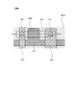
図6は、本実施形態に係る表示装置が有する画素109aの構成を説明する拡大平面図である。図7は、図3のA1-A2間の断面図、図6のB1-B2間の断面図を示している。
第1実施形態に係る表示装置100の画素109と本実施形態に係る表示装置の画素109aとを比較すると、本実施形態に係る表示装置の画素109aに示す絶縁層224aは、半導体層225の全領域に亘って配置される点で異なっている。
このような構成を有することによって、半導体層225の外部から半導体層225の内部への水素の侵入することをより抑制することができる。これによって、トランジスタ220のキャリア移動度の低減を防止し、閾値ばらつきを抑制することができる等、トランジスタ220の特性劣化を防ぐことができる。これによって、信頼性が向上し、長寿命の表示装置を提供することができる。
本実施形態においては、絶縁層224aは、島状の半導体層225と重畳するように配置されている。つまり、島状の半導体層225の面積と、絶縁層224aの面積とがほぼ同じである。しかし、絶縁層224aのレイアウトはこれに限られるものではない。絶縁層224aは、平面視において少なくとも島状の半導体層225と重畳していればよいため、島状の半導体層225の面積よりも、絶縁層224aの面積の方が大きくてもよい。
本実施形態で示す絶縁層224a及び島状の半導体層225は、次のようにして形成される。まず、層間絶縁層223上に、CVD法によりダイヤモンドライクカーボンを成膜し、スパッタリング法により、酸化物半導体を成膜した後、エッチング法により、ダイヤモンドライクカーボンと酸化物半導体とを加工することにより、絶縁層224aと半導体層225とを形成することができる。絶縁層224aと半導体層225とを一度に加工することができるため、第1実施形態よりも工程数を削減することができる。
つまり、絶縁層244aは、島状の半導体層225の領域内からその外部に延長された領域に亘って配置されてもよい。例えば、少なくとも2つの酸化物半導体層に亘って配置されていてもよい。また、絶縁層244aは、半導体層225の領域の周縁部から所定の距離まで延長された領域に亘って配置されてもよい。
<第3実施形態>
本実施形態では、第1実施形態に係る表示装置100とは一部異なる構成を有する表示装置について、図8及び図9を参照して説明する。なお、第1実施形態に係る表示装置100と共通の構成については説明を省略する。
本実施形態では、第1実施形態に係る表示装置100とは一部異なる構成を有する表示装置について、図8及び図9を参照して説明する。なお、第1実施形態に係る表示装置100と共通の構成については説明を省略する。
図8は、本実施形態に係る表示装置が有する画素109の構成を説明する拡大平面図である。図9は、図3のA1-A2間の断面図、図8のB1-B2間の断面図を示している。
第1実施形態に係る表示装置100の画素109と本実施形態に係る表示装置の画素109bとを比較すると、本実施形態に係る表示装置の画素109bに示す絶縁層224bは、表示領域103の全領域に亘って配置される点で異なっている。
このような構成を有することによって、半導体層225の外部から半導体層225の内部への水素の侵入することをより抑制することができる。これによって、トランジスタ220のキャリア移動度の低減を防止し、閾値ばらつきを抑制することができる等、トランジスタ220の特性劣化を防ぐことができる。これによって、信頼性が向上し、長寿命の表示装置を提供することができる。
更に、本実施形態のように、表示領域103の全領域に亘って絶縁層224bを設けることにより、パターニング工程が省略され、製造工程を簡略化することができる。更に、絶縁層224bが層間絶縁層として機能するため、層間絶縁層223を薄膜化することができる。これによって、材料のコスト削減や、タクトタイムの短縮、そしてコンタクトホールの形成が容易になる。
<第4実施形態>
本実施形態では、第1実施形態に係る表示装置100とは一部異なる構成を有する表示装置について、図10及び図11を参照して説明する。なお、第1実施形態に係る表示装置100と共通の構成については説明を省略する。
本実施形態では、第1実施形態に係る表示装置100とは一部異なる構成を有する表示装置について、図10及び図11を参照して説明する。なお、第1実施形態に係る表示装置100と共通の構成については説明を省略する。
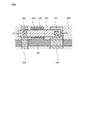
図10は、本実施形態に係る表示装置が有する画素109cの構成を説明する拡大平面図である。図11は、図3のA1-A2間の断面図、図10のB1-B2間の断面図を示している。
第1実施形態に係る表示装置100の画素109と本実施形態に係る表示装置の画素109cとを比較すると、本実施形態に係る表示装置100の画素109cは、複数の画素109cの各々において、絶縁層246を更に備えている。絶縁層246は、トランジスタ220上においてチャネル領域と重畳して配置される。また、絶縁層246として、ダイヤモンドライクカーボンを用いることができる。
また、絶縁層246に含有される水素濃度は、層間絶縁層223に含有される水素濃度のよりも低いことが好ましい。このように、酸化物半導体である半導体層225により近いほど水素濃度を低くすることで、酸化物半導体に水素が侵入することを抑制することができる。
このような構成を有することによって、半導体層225の外部から半導体層225の内部への水素の侵入することをより抑制することができる。これによって、トランジスタ220のキャリア移動度の低減を防止し、閾値ばらつきを抑制することができる等、トランジスタ220の特性劣化を防ぐことができる。これによって、信頼性が向上し、長寿命の表示装置を提供することができる。
さらに、このような構成を有することによって、半導体層225の上部から半導体層225への水素の侵入することをより抑制することができる。これによって、トランジスタ220のチャネル移動度の低減を防止し、閾値ばらつきを抑制することができる等、トランジスタ220の特性劣化を防ぐことができる。これによって、信頼性が向上し、長寿命の表示装置を提供することができる。
また、本実施形態では、複数の画素109の各々において、絶縁層246を備えている例を示したが、本発明はこれに限定されない。例えば、表示領域103の全領域に亘って絶縁層246が設けられていてもよい。これにより、トランジスタ220の下側と上側の両方から、水素の侵入や透過を抑制することができるため、好ましい。
また、本実施形態では、表示領域103の全領域に亘って、絶縁層224が設けられる例を示したが、本発明はこれに限定されない。例えば、図5に示すように、絶縁層244は、少なくともチャネル領域と重畳していてもよいし、半導体層225の全領域に亘って配置されていてもよい。
以上、本発明のいくつかの実施形態について説明したが、本発明は、上記の実施形態に限定されることなく、本発明の主旨を逸脱しない範囲で種々の変更が可能であり、それらも本発明の範囲内に包含されるものであることはいうまでもない。
100:表示装置、101:基板、102:対向基板、103:表示領域、104:走査線駆動回路、106:ドライバIC、107:端子、108:フレキシブルプリント基板、109:画素、110:周辺領域、111:走査線、112:信号線、113:駆動電源線、114:基準電源線、210:トランジスタ、211:下地膜、212:半導体層、213:ゲート絶縁膜、214:ゲート電極、215:層間絶縁層、216:コンタクトホール、217:コンタクトホール、218:ソース電極又はドレイン電極、219:ソース電極又はドレイン電極、220:トランジスタ、221:半導体層、222:コンタクトホール、223:層間絶縁層、224:絶縁層、224a:絶縁層、224b:絶縁層、225:半導体層、226:ゲート絶縁膜、227:ゲート電極、228:層間絶縁層、229:コンタクトホール、230:保持容量、231:コンタクトホール、232:ソース電極又はドレイン電極、233:ソース電極又はドレイン電極、234:平坦化膜、235:画素電極、236:コンタクトホール、237:導電層、238:コンタクトホール、239:導電層、240:発光素子、241:コンタクトホール、242:有機層、243:陰極、244:絶縁層、245:コンタクトホール、246:絶縁層、247:導電層、248:コンタクトホール
Claims (11)
- 表示領域を有する基板と、
前記基板の前記表示領域に配列された複数の画素と、を備え、
前記複数の画素の各々は、発光素子、第1トランジスタ、第2トランジスタ、第1絶縁層、及び第2絶縁層を含み、
前記第1トランジスタは、シリコン層を有し、
前記第2トランジスタは、前記第1絶縁層よりも上層に配置された酸化物半導体層を有し、
前記第1絶縁層は、酸化シリコン層を含み、
前記第1絶縁層は、前記シリコン層と、前記酸化物半導体層との間に、前記複数の画素に共通して前記表示領域に亘って配置され、
前記第2絶縁層は、ダイヤモンドライクカーボンを含み、
前記第2絶縁層は、前記第2トランジスタのチャネル領域と、前記第1絶縁層との間に配置される、表示装置。 - 前記シリコン層は、多結晶シリコンである請求項1に記載の表示装置。
- 前記第1トランジスタは、駆動トランジスタであり、
前記第2トランジスタは、選択トランジスタである請求項1に記載の表示装置。 - 前記第2トランジスタは、トップゲート構造を有することを特徴とする請求項1に記載の表示装置。
- 前記第2絶縁層は、前記酸化物半導体層の全領域に亘って配置される、請求項1に記載の表示装置。
- 前記第2絶縁層は、少なくとも2つの前記酸化物半導体層に亘って配置される、請求項1に記載の表示装置。
- 前記第2絶縁層は、前記表示領域の全領域に亘って配置される、請求項1に記載の表示装置。
- 前記第2絶縁層は、前記酸化物半導体層に接して配置される、請求項1に記載の表示装置。
- 前記第2絶縁層に含有される水素濃度は、前記第1絶縁層に含有される水素濃度よりも低い、請求項1に記載の表示装置。
- 第3絶縁層をさらに有し、
前記第3絶縁層は、ダイヤモンドライクカーボンを含み、
前記第3絶縁層は、前記第2トランジスタの上において前記チャネル領域と重畳して配置される、請求項1に記載の表示装置。 - 前記第3絶縁層に含有される水素濃度は、前記第1絶縁層に含有される水素濃度よりも低い、請求項10に記載の表示装置。
Applications Claiming Priority (2)
| Application Number | Priority Date | Filing Date | Title |
|---|---|---|---|
| JP2017-188473 | 2017-09-28 | ||
| JP2017188473A JP2019066517A (ja) | 2017-09-28 | 2017-09-28 | 表示装置 |
Publications (1)
| Publication Number | Publication Date |
|---|---|
| WO2019064744A1 true WO2019064744A1 (ja) | 2019-04-04 |
Family
ID=65901271
Family Applications (1)
| Application Number | Title | Priority Date | Filing Date |
|---|---|---|---|
| PCT/JP2018/023622 Ceased WO2019064744A1 (ja) | 2017-09-28 | 2018-06-21 | 表示装置 |
Country Status (2)
| Country | Link |
|---|---|
| JP (1) | JP2019066517A (ja) |
| WO (1) | WO2019064744A1 (ja) |
Cited By (1)
| Publication number | Priority date | Publication date | Assignee | Title |
|---|---|---|---|---|
| JP2023088927A (ja) * | 2020-11-10 | 2023-06-27 | エルジー ディスプレイ カンパニー リミテッド | 表示装置 |
Families Citing this family (3)
| Publication number | Priority date | Publication date | Assignee | Title |
|---|---|---|---|---|
| CN111180478B (zh) * | 2019-12-26 | 2022-05-13 | 华灿光电(苏州)有限公司 | 微型发光二极管外延片、显示阵列及其制作方法 |
| KR102845809B1 (ko) | 2020-04-29 | 2025-08-13 | 삼성디스플레이 주식회사 | 표시 패널 및 이를 구비한 표시 장치 |
| CN115116396B (zh) | 2022-07-28 | 2024-08-06 | 惠科股份有限公司 | 像素驱动电路和显示面板 |
Citations (7)
| Publication number | Priority date | Publication date | Assignee | Title |
|---|---|---|---|---|
| JPH06214128A (ja) * | 1993-01-19 | 1994-08-05 | Nippon Telegr & Teleph Corp <Ntt> | 光導波回路 |
| JP2007123861A (ja) * | 2005-09-29 | 2007-05-17 | Semiconductor Energy Lab Co Ltd | 半導体装置及びその作製方法 |
| JP2010232651A (ja) * | 2009-03-05 | 2010-10-14 | Semiconductor Energy Lab Co Ltd | 半導体装置 |
| US20120018721A1 (en) * | 2010-07-26 | 2012-01-26 | Snu R&Db Foundation | Thin film transistor and method for fabricating thin film transistor |
| JP2013180501A (ja) * | 2012-03-02 | 2013-09-12 | Hyomen Kino Design Kenkyusho Kk | 水素透過防止被膜 |
| JP2015156486A (ja) * | 2014-02-19 | 2015-08-27 | 三星ディスプレイ株式會社Samsung Display Co.,Ltd. | 有機発光ディスプレイ装置 |
| WO2016048385A1 (en) * | 2014-09-24 | 2016-03-31 | Apple Inc. | Silicon and semiconducting oxide thin-film transistor displays |
-
2017
- 2017-09-28 JP JP2017188473A patent/JP2019066517A/ja active Pending
-
2018
- 2018-06-21 WO PCT/JP2018/023622 patent/WO2019064744A1/ja not_active Ceased
Patent Citations (7)
| Publication number | Priority date | Publication date | Assignee | Title |
|---|---|---|---|---|
| JPH06214128A (ja) * | 1993-01-19 | 1994-08-05 | Nippon Telegr & Teleph Corp <Ntt> | 光導波回路 |
| JP2007123861A (ja) * | 2005-09-29 | 2007-05-17 | Semiconductor Energy Lab Co Ltd | 半導体装置及びその作製方法 |
| JP2010232651A (ja) * | 2009-03-05 | 2010-10-14 | Semiconductor Energy Lab Co Ltd | 半導体装置 |
| US20120018721A1 (en) * | 2010-07-26 | 2012-01-26 | Snu R&Db Foundation | Thin film transistor and method for fabricating thin film transistor |
| JP2013180501A (ja) * | 2012-03-02 | 2013-09-12 | Hyomen Kino Design Kenkyusho Kk | 水素透過防止被膜 |
| JP2015156486A (ja) * | 2014-02-19 | 2015-08-27 | 三星ディスプレイ株式會社Samsung Display Co.,Ltd. | 有機発光ディスプレイ装置 |
| WO2016048385A1 (en) * | 2014-09-24 | 2016-03-31 | Apple Inc. | Silicon and semiconducting oxide thin-film transistor displays |
Cited By (3)
| Publication number | Priority date | Publication date | Assignee | Title |
|---|---|---|---|---|
| JP2023088927A (ja) * | 2020-11-10 | 2023-06-27 | エルジー ディスプレイ カンパニー リミテッド | 表示装置 |
| US12364126B2 (en) | 2020-11-10 | 2025-07-15 | Lg Display Co., Ltd. | Display device |
| JP7742374B2 (ja) | 2020-11-10 | 2025-09-19 | エルジー ディスプレイ カンパニー リミテッド | 表示装置 |
Also Published As
| Publication number | Publication date |
|---|---|
| JP2019066517A (ja) | 2019-04-25 |
Similar Documents
| Publication | Publication Date | Title |
|---|---|---|
| US8144086B2 (en) | Organic light emitting display device | |
| US10861916B2 (en) | Display substrate, manufacturing method thereof and display panel | |
| US9064833B2 (en) | Organic light emitting diode display | |
| US8004178B2 (en) | Organic light emitting diode display with a power line in a non-pixel region | |
| KR102351664B1 (ko) | 유기 발광 표시 장치 | |
| CN102105924B (zh) | 显示装置以及显示装置的制造方法 | |
| US20100102713A1 (en) | Organic light emitting display device | |
| US11081663B2 (en) | Organic electroluminescent display panel with auxiliary electrodes, method for manufacturing the same, and display device using the same | |
| US10276723B2 (en) | Flexible display | |
| CN1592518A (zh) | 有机电致发光显示装置 | |
| KR20110111746A (ko) | 유기 발광 표시 장치 | |
| JP2018010234A (ja) | 表示装置 | |
| WO2019156024A1 (ja) | 表示装置 | |
| JP2018088346A (ja) | 表示装置 | |
| JP2008123986A (ja) | 有機電界発光表示装置 | |
| CN110164942A (zh) | 一种显示面板及其制备方法、显示装置 | |
| WO2019064744A1 (ja) | 表示装置 | |
| KR100879294B1 (ko) | 유기 발광 표시 장치 | |
| CN111490076B (zh) | 导线、包括导线的显示装置和制造显示装置的方法 | |
| JP2016197580A (ja) | 有機el表示装置 | |
| KR20080104875A (ko) | 유기전계발광표시장치 | |
| US9337440B2 (en) | Organic luminescent display device | |
| US12581803B2 (en) | Display device and method of manufacturing the same | |
| US8575598B2 (en) | Organic light emitting diode display | |
| US12532623B2 (en) | Display device and method of repairing the same |
Legal Events
| Date | Code | Title | Description |
|---|---|---|---|
| 121 | Ep: the epo has been informed by wipo that ep was designated in this application |
Ref document number: 18860811 Country of ref document: EP Kind code of ref document: A1 |
|
| NENP | Non-entry into the national phase |
Ref country code: DE |
|
| 122 | Ep: pct application non-entry in european phase |
Ref document number: 18860811 Country of ref document: EP Kind code of ref document: A1 |