WO2019064672A1 - 皮膜積層体及びその製造方法 - Google Patents
皮膜積層体及びその製造方法 Download PDFInfo
- Publication number
- WO2019064672A1 WO2019064672A1 PCT/JP2018/017692 JP2018017692W WO2019064672A1 WO 2019064672 A1 WO2019064672 A1 WO 2019064672A1 JP 2018017692 W JP2018017692 W JP 2018017692W WO 2019064672 A1 WO2019064672 A1 WO 2019064672A1
- Authority
- WO
- WIPO (PCT)
- Prior art keywords
- film
- nickel alloy
- sulfur
- concentration
- film laminate
- Prior art date
- Legal status (The legal status is an assumption and is not a legal conclusion. Google has not performed a legal analysis and makes no representation as to the accuracy of the status listed.)
- Ceased
Links
Images




Classifications
-
- B—PERFORMING OPERATIONS; TRANSPORTING
- B32—LAYERED PRODUCTS
- B32B—LAYERED PRODUCTS, i.e. PRODUCTS BUILT-UP OF STRATA OF FLAT OR NON-FLAT, e.g. CELLULAR OR HONEYCOMB, FORM
- B32B15/00—Layered products comprising a layer of metal
- B32B15/01—Layered products comprising a layer of metal all layers being exclusively metallic
-
- B—PERFORMING OPERATIONS; TRANSPORTING
- B32—LAYERED PRODUCTS
- B32B—LAYERED PRODUCTS, i.e. PRODUCTS BUILT-UP OF STRATA OF FLAT OR NON-FLAT, e.g. CELLULAR OR HONEYCOMB, FORM
- B32B15/00—Layered products comprising a layer of metal
- B32B15/04—Layered products comprising a layer of metal comprising metal as the main or only constituent of a layer, which is next to another layer of the same or of a different material
-
- C—CHEMISTRY; METALLURGY
- C25—ELECTROLYTIC OR ELECTROPHORETIC PROCESSES; APPARATUS THEREFOR
- C25D—PROCESSES FOR THE ELECTROLYTIC OR ELECTROPHORETIC PRODUCTION OF COATINGS; ELECTROFORMING; APPARATUS THEREFOR
- C25D5/00—Electroplating characterised by the process; Pretreatment or after-treatment of workpieces
- C25D5/10—Electroplating with more than one layer of the same or of different metals
- C25D5/12—Electroplating with more than one layer of the same or of different metals at least one layer being of nickel or chromium
- C25D5/14—Electroplating with more than one layer of the same or of different metals at least one layer being of nickel or chromium two or more layers being of nickel or chromium, e.g. duplex or triplex layers
-
- C—CHEMISTRY; METALLURGY
- C25—ELECTROLYTIC OR ELECTROPHORETIC PROCESSES; APPARATUS THEREFOR
- C25D—PROCESSES FOR THE ELECTROLYTIC OR ELECTROPHORETIC PRODUCTION OF COATINGS; ELECTROFORMING; APPARATUS THEREFOR
- C25D5/00—Electroplating characterised by the process; Pretreatment or after-treatment of workpieces
- C25D5/48—After-treatment of electroplated surfaces
- C25D5/50—After-treatment of electroplated surfaces by heat-treatment
-
- C—CHEMISTRY; METALLURGY
- C25—ELECTROLYTIC OR ELECTROPHORETIC PROCESSES; APPARATUS THEREFOR
- C25D—PROCESSES FOR THE ELECTROLYTIC OR ELECTROPHORETIC PRODUCTION OF COATINGS; ELECTROFORMING; APPARATUS THEREFOR
- C25D5/00—Electroplating characterised by the process; Pretreatment or after-treatment of workpieces
- C25D5/60—Electroplating characterised by the structure or texture of the layers
- C25D5/605—Surface topography of the layers, e.g. rough, dendritic or nodular layers
- C25D5/611—Smooth layers
-
- C—CHEMISTRY; METALLURGY
- C25—ELECTROLYTIC OR ELECTROPHORETIC PROCESSES; APPARATUS THEREFOR
- C25D—PROCESSES FOR THE ELECTROLYTIC OR ELECTROPHORETIC PRODUCTION OF COATINGS; ELECTROFORMING; APPARATUS THEREFOR
- C25D5/00—Electroplating characterised by the process; Pretreatment or after-treatment of workpieces
- C25D5/60—Electroplating characterised by the structure or texture of the layers
- C25D5/615—Microstructure of the layers, e.g. mixed structure
- C25D5/617—Crystalline layers
-
- C—CHEMISTRY; METALLURGY
- C25—ELECTROLYTIC OR ELECTROPHORETIC PROCESSES; APPARATUS THEREFOR
- C25D—PROCESSES FOR THE ELECTROLYTIC OR ELECTROPHORETIC PRODUCTION OF COATINGS; ELECTROFORMING; APPARATUS THEREFOR
- C25D3/00—Electroplating: Baths therefor
- C25D3/02—Electroplating: Baths therefor from solutions
- C25D3/56—Electroplating: Baths therefor from solutions of alloys
- C25D3/562—Electroplating: Baths therefor from solutions of alloys containing more than 50% by weight of iron or nickel or cobalt
-
- Y—GENERAL TAGGING OF NEW TECHNOLOGICAL DEVELOPMENTS; GENERAL TAGGING OF CROSS-SECTIONAL TECHNOLOGIES SPANNING OVER SEVERAL SECTIONS OF THE IPC; TECHNICAL SUBJECTS COVERED BY FORMER USPC CROSS-REFERENCE ART COLLECTIONS [XRACs] AND DIGESTS
- Y10—TECHNICAL SUBJECTS COVERED BY FORMER USPC
- Y10T—TECHNICAL SUBJECTS COVERED BY FORMER US CLASSIFICATION
- Y10T428/00—Stock material or miscellaneous articles
- Y10T428/12—All metal or with adjacent metals
- Y10T428/12014—All metal or with adjacent metals having metal particles
- Y10T428/12028—Composite; i.e., plural, adjacent, spatially distinct metal components [e.g., layers, etc.]
- Y10T428/12049—Nonmetal component
-
- Y—GENERAL TAGGING OF NEW TECHNOLOGICAL DEVELOPMENTS; GENERAL TAGGING OF CROSS-SECTIONAL TECHNOLOGIES SPANNING OVER SEVERAL SECTIONS OF THE IPC; TECHNICAL SUBJECTS COVERED BY FORMER USPC CROSS-REFERENCE ART COLLECTIONS [XRACs] AND DIGESTS
- Y10—TECHNICAL SUBJECTS COVERED BY FORMER USPC
- Y10T—TECHNICAL SUBJECTS COVERED BY FORMER US CLASSIFICATION
- Y10T428/00—Stock material or miscellaneous articles
- Y10T428/12—All metal or with adjacent metals
- Y10T428/12014—All metal or with adjacent metals having metal particles
- Y10T428/12028—Composite; i.e., plural, adjacent, spatially distinct metal components [e.g., layers, etc.]
- Y10T428/12063—Nonparticulate metal component
- Y10T428/12069—Plural nonparticulate metal components
-
- Y—GENERAL TAGGING OF NEW TECHNOLOGICAL DEVELOPMENTS; GENERAL TAGGING OF CROSS-SECTIONAL TECHNOLOGIES SPANNING OVER SEVERAL SECTIONS OF THE IPC; TECHNICAL SUBJECTS COVERED BY FORMER USPC CROSS-REFERENCE ART COLLECTIONS [XRACs] AND DIGESTS
- Y10—TECHNICAL SUBJECTS COVERED BY FORMER USPC
- Y10T—TECHNICAL SUBJECTS COVERED BY FORMER US CLASSIFICATION
- Y10T428/00—Stock material or miscellaneous articles
- Y10T428/12—All metal or with adjacent metals
- Y10T428/12014—All metal or with adjacent metals having metal particles
- Y10T428/12028—Composite; i.e., plural, adjacent, spatially distinct metal components [e.g., layers, etc.]
- Y10T428/12063—Nonparticulate metal component
- Y10T428/12069—Plural nonparticulate metal components
- Y10T428/12076—Next to each other
-
- Y—GENERAL TAGGING OF NEW TECHNOLOGICAL DEVELOPMENTS; GENERAL TAGGING OF CROSS-SECTIONAL TECHNOLOGIES SPANNING OVER SEVERAL SECTIONS OF THE IPC; TECHNICAL SUBJECTS COVERED BY FORMER USPC CROSS-REFERENCE ART COLLECTIONS [XRACs] AND DIGESTS
- Y10—TECHNICAL SUBJECTS COVERED BY FORMER USPC
- Y10T—TECHNICAL SUBJECTS COVERED BY FORMER US CLASSIFICATION
- Y10T428/00—Stock material or miscellaneous articles
- Y10T428/12—All metal or with adjacent metals
- Y10T428/12014—All metal or with adjacent metals having metal particles
- Y10T428/12028—Composite; i.e., plural, adjacent, spatially distinct metal components [e.g., layers, etc.]
- Y10T428/12063—Nonparticulate metal component
- Y10T428/12069—Plural nonparticulate metal components
- Y10T428/12076—Next to each other
- Y10T428/12083—Nonmetal in particulate component
-
- Y—GENERAL TAGGING OF NEW TECHNOLOGICAL DEVELOPMENTS; GENERAL TAGGING OF CROSS-SECTIONAL TECHNOLOGIES SPANNING OVER SEVERAL SECTIONS OF THE IPC; TECHNICAL SUBJECTS COVERED BY FORMER USPC CROSS-REFERENCE ART COLLECTIONS [XRACs] AND DIGESTS
- Y10—TECHNICAL SUBJECTS COVERED BY FORMER USPC
- Y10T—TECHNICAL SUBJECTS COVERED BY FORMER US CLASSIFICATION
- Y10T428/00—Stock material or miscellaneous articles
- Y10T428/12—All metal or with adjacent metals
- Y10T428/12014—All metal or with adjacent metals having metal particles
- Y10T428/12028—Composite; i.e., plural, adjacent, spatially distinct metal components [e.g., layers, etc.]
- Y10T428/12063—Nonparticulate metal component
- Y10T428/12104—Particles discontinuous
- Y10T428/12111—Separated by nonmetal matrix or binder [e.g., welding electrode, etc.]
- Y10T428/12118—Nonparticulate component has Ni-, Cu-, or Zn-base
Definitions
- the present invention relates to a film laminate in which a plurality of films are laminated on a substrate, and a method of manufacturing the same.
- hexavalent chromium has been designated as a substance of high environmental concern in environmental regulations and drainage regulations such as REACH regulations (Regulation concerned with Registration, Evaluation, Authorization and Restriction of Chemicals, establishing a European Chemicals Agency), and its use reduction Is desired globally. Under such circumstances, various surface treatment techniques have been proposed as plating techniques to replace hexavalent chromium plating.
- Patent Document 1 a plurality of Ni alloy plating films are formed on the surface of a material to be plated, and each layer Ni alloy plating film contains elements selected from P, B, and S at different concentrations, and adjacent Ni There is disclosed a multilayer Ni alloy plating film or the like in which the electric potential relationship between the alloy plating films is provided such that the outer Ni alloy plating film is 30 mV or more higher than the inner Ni plating film.
- Patent Document 1 is a multilayer Ni alloy plating film for the purpose of improving corrosion resistance and productivity, and plating of each layer by changing the current density with one plating bath in order to express a sacrificial anticorrosive action by an interlayer potential difference.
- the content of metalloid elements such as P in the film is adjusted.
- the hardness was different for each layer of the multilayer plating film, and it could not be said that the wear resistance as the whole multilayer plating film was sufficient. That is, further improvement is required with respect to the wear resistance of the film.
- One aspect of the present invention is a laminate in which a plurality of layers of films are laminated on a substrate, and the plurality of layers of films are layers of a plurality of sulfur (S) -containing nickel (Ni) alloy films And a sulfur-enriched layer formed between layers of the plurality of S-containing Ni alloy films and having an S concentration higher than the S concentration of the S-containing Ni alloy film, each film of the plurality of S-containing Ni alloy films
- the present invention provides a film laminate characterized in that the Ni concentration is 90% by mass or more, and the difference in the Ni concentration of each film is within 1% by mass.
- the present invention can make the following improvements and changes in the above-mentioned film laminate (I).
- the S concentration of the sulfur-enriched layer is 102% or more of the S concentration of the plurality of S-containing Ni alloy coatings.
- Each film of the plurality of S-containing Ni alloy films has the same thickness.
- Each film of the plurality of S-containing Ni alloy films has a thickness of 300 nm or more and 1000 nm or less.
- Each film of the plurality of S-containing Ni alloy films further contains phosphorus (P).
- Each film of the plurality of S-containing Ni alloy films has an average crystal grain size of 8 nm or less.
- Another aspect of the present invention is a method for producing a film laminate as described above, comprising a plurality of nickel alloy plating steps and an annealing step, wherein the annealing step comprises annealing temperature Is a temperature of 300 ° C. or less.
- the present invention can make the following improvements and changes in the method (II) for producing a film laminate described above.
- (Vi) A plating process stopping step is interposed between the plurality of nickel alloy plating process steps.
- stacked on a base material can be provided.
- FIG. 1 It is a schematic cross-sectional schematic diagram which shows an example of the film
- FIG. 1 It is a schematic cross-sectional schematic diagram which shows an example of the film
- FIG. 1 is a schematic cross-sectional schematic view showing an example of a film laminate according to the present invention.
- a multilayer film 1 is formed on the surface of a substrate 2.
- two layers of the sulfur-containing nickel alloy film 3 and the sulfur-containing nickel alloy film 4 are laminated.
- the "sulfur-containing nickel alloy film” may be simply referred to as the "nickel alloy film”.
- the base material 2 which forms the multilayer film 1 there is no limitation in particular in the base material 2 which forms the multilayer film 1, and it can be suitably selected according to the use of a film layered product.
- carbon steel, low alloy steel, stainless steel, copper, aluminum, alloys thereof and the like can be appropriately used.
- the feature of the film laminate of the present invention is that, in the multilayer film 1, the sulfur-containing nickel alloy films 3 and 4 are formed between the adjacent sulfur-containing nickel alloy film 3 and the sulfur-containing nickel alloy film 4 (interface region). It is to provide the sulfur concentration layer 5 which has S concentration higher than S concentration.
- the sulfur concentrated layer 5 having a sacrificial corrosion protection function is provided between the films of the multilayer film 1 (the interface region of adjacent films), so that the film thickness direction (perpendicular to the film) is usually Pitting that proceeds in the direction) can be converted in the direction parallel to the film (horizontal direction to the film), whereby the corrosion reaching the substrate 2 can be suppressed.
- the sulfur-enriched layer 5 as the constituent layer of the multilayer coating 1, it is possible to improve the corrosion resistance of the coating laminate.
- the S concentration of the sulfur concentrated layer 5 is preferably higher than the S concentration of the adjacent sulfur-containing nickel alloy coatings 3 and 4, and more specifically, desirably 102% or more.
- a metalloid element for example, phosphorus (P), boron (B)
- P phosphorus
- B boron
- particles of oxide eg, titanium oxide (TiO 2 ), aluminum oxide (Al 2 O 3 )
- carbide eg, silicon carbide (SiC)
- P it is desirable to contain P as a component of the nickel alloy. In this case, it is desirable that the P concentration be the same in each nickel alloy film.
- each nickel alloy film preferably has a smaller crystal grain size from the viewpoint of enhancing the hardness (that is, from the viewpoint of enhancing the wear resistance), and more specifically, the average grain size is 4 nm to 8 nm. Is desirable, and more desirably 6 nm or more and 8 nm or less.
- each nickel alloy film is preferably 300 nm or more and 1000 nm or less. Furthermore, it is desirable to make the thickness of each nickel alloy film uniform (equal).
- FIG. 8 is a graph showing the relationship between the thickness of each NiP layer and the hardness (Vickers hardness) of the multilayer film when the nickel alloy film (here, NiP layer) having the same thickness is multilayered.
- Each test sample had a sulfur-enriched layer between the NiP layers, and the number of layers was adjusted so that the total thickness of the multilayer film was about 10 ⁇ m.
- the Vickers hardness of the multilayer film 1 can be increased to 800 HV or more by making the thickness of each nickel alloy film equal within the range of 300 nm to 1000 nm. That is, the wear resistance can be improved by controlling the thickness of each alloy film to the above range. Further, by unifying the thickness of each alloy film, manufacturing control can be facilitated and productivity improvement can also be expected. Unfortunately, the cause of this result has not been elucidated at this stage.
- Method of manufacturing film laminate The manufacturing method of the film laminated body which concerns on this invention is demonstrated.
- a method for producing a film laminate of the present invention a method for forming a multilayer film
- treatment methods such as wet treatment (for example, electroplating) and dry treatment (for example, sputtering) can be used. From the viewpoint of mass productivity, electroplating is a preferred form.
- the electroplating solution for forming the multi-layered coating 1 is not particularly limited, and it is prepared by adding an alloy component and a sulfur-containing organic compound to a watt bath mainly composed of nickel sulfate, nickel chloride, boric acid and the like. can do.
- a sulfur-containing organic compound for example, when using phosphorus as an alloy component, phosphonic acid etc. can be added.
- known brighteners such as saccharin, sodium lauryl sulfate, allyl sulfonic acid, thiourea and the like can be used.
- the nickel alloy film is hardened and smoothed, and the wear resistance of the multilayer film 1 is improved.
- the concentration of various components of the electroplating solution can be adjusted appropriately.
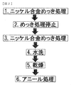
- FIG. 2 is a flow chart showing an example of a method of producing a film laminate according to the present invention, which shows an electroplating process. As shown in FIG. 2, the manufacturing process of the film laminate is performed in the following order.
- Step of plating nickel alloy film 3 Plating stop step 3.
- Step of plating nickel alloy film 4 4. Washing step 5. Drying step 6. Annealing step.
- FIG. 2 it described about the multilayer film 1 which laminated
- the number of layers of the nickel alloy film can be appropriately set in accordance with the specifications such as the properties and life. In that case, the above steps 1 to 3 may be repeated as appropriate depending on the number of layers of the nickel alloy film of the multilayer film 1.
- the process 2 in the above process is carried out.
- the annealing step is important.
- the plating process stopping step it is preferable to make the plating process stop time 30 seconds or more while being immersed in the plating solution. This is a finding obtained from the results of intensive researches conducted by the present inventors, and is the time required for the sulfur-containing organic compound to be sufficiently adsorbed on the surface of the nickel alloy film 3.
- the sulfur concentration layer 5 can be formed on the surface of the nickel alloy film 3 (the interface region of the nickel alloy films 3 and 4 later) by setting the plating stop time of the plating process stopping step to be 30 seconds or more. Moreover, it has been confirmed that the hardness of the multilayer film 1 changes with the plating stop time.
- FIG. 3 is a graph showing an example of the relationship between the plating stop time of the plating process stopping step and the hardness (Vickers hardness) of the multilayer film.
- the plating stop time of the plating process stopping step is stopped, an example in which the material to be plated is immediately taken out of the plating solution and washed with water (that is, an example in which the plating stop time while immersed in the plating solution is 0 seconds) is also shown.
- the Vickers hardness of the multilayer film 1 is improved by setting the plating stop time to 30 seconds or more while immersing the material to be plated in the plating solution.
- the plating process is stopped, it is confirmed that the Vickers hardness decreases in the sample (sample with water washing) in which the material to be plated is immediately taken out of the plating solution and washed with water.
- the coarsening of the crystal grain of the nickel alloy film is suppressed in the annealing treatment step of the post process due to the presence of the sulfur concentrated layer 5. More specifically, it is conceivable that the coarsening of the crystal grains of the adjacent nickel alloy films 3 and 4 is suppressed by the diffusion and permeation of the sulfur component from the sulfur-rich layer 5.
- the annealing temperature is preferably 200 ° C. or more and 300 ° C. or less. This is a finding obtained from the results of intensive research conducted by the present inventors. By setting the annealing temperature to 300 ° C. or less, the average crystal grain size of the nickel alloy film can be maintained to 8 nm or less. If the annealing temperature is less than 200 ° C., the improvement in hardness of the multilayer film 1 will be insufficient. When the annealing temperature exceeds 300 ° C., the crystal grains of the nickel alloy film tend to be coarsened, and the hardness of the multilayer film 1 is lowered.
- the annealing treatment time is not particularly limited, but for example, 1 hour or more is preferable.
- the electrolytic conditions of the plating process step of the nickel alloy film 4 may be appropriately adjusted from the viewpoint of unifying the thickness of each film, as long as the current density and the processing time may be appropriately adjusted according to the desired film thickness. preferable.
- an impurity removal step such as degreasing or pickling may be performed prior to the plating treatment step of the nickel alloy film 3, as a pretreatment of the base material 2.
- the method for producing a film laminate of the present invention is simple and has high productivity because it forms a plurality of layers of a nickel alloy film under the same electrolytic conditions using one plating bath (that is, low in productivity). There is an advantage of cost).
- the shape of the substrate 2 i.e., the shape of the film laminate
- the shape of the substrate 2 is not particularly limited, and can be applied to components of any shape (e.g., lumps, flat plates, curved plates, cylinders, prisms).
- the film thickness may vary depending on the location due to the influence of the current distribution. Therefore, the influence of the current distribution is measured in advance by analysis and measurement, and if necessary, a shield plate etc. is installed between the object to be plated and the counter electrode, etc. to suppress the variation of the film thickness due to the plating location. It is preferable to carry out under the conditions that can be performed.
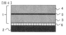
- FIG. 4 is a schematic cross-sectional schematic view showing another example of the film laminate according to the present invention.
- an adhesion layer 6 may be provided between the substrate 2 and the sulfur-containing nickel alloy film 3 depending on the type of the substrate 2. This is effective when the substrate 2 is made of a material that forms a stable oxide film or the like on the surface thereof.
- the adhesion of the sulfur-containing nickel alloy film 3 to the substrate 2 tends to be weak. Therefore, it is preferable to improve the adhesion by providing the adhesion layer 6 between the base material 2 and the sulfur-containing nickel alloy film 3 (that is, on the surface of the base material 2).
- the adhesion layer 6 can be formed on the surface of the base material 2 using a wood bath.
- the target component of the nickel alloy was phosphorus, and phosphonic acid was used.
- the sulfur-containing organic compound was saccharin.
- the production process of the film laminate was performed along FIG. Specifically, first, as a pretreatment of the base material, an impurity removal step of degreasing and pickling was performed.
- the thickness of each film was 500 nm, and the number of layers was 20 (the number of repetition of the plating step was 20). That is, the thickness of the multi-layered film as a whole is 10 ⁇ m.
- the electrolytic conditions of the plating step were performed at a constant current using a Ni plate as a counter electrode.
- the stop time is 30 seconds.
- the annealing temperature is 300 ° C., and the holding time is 2 hours.
- the film laminate of Example 1 was produced by the above procedure.
- Example 2 (Preparation of Example 2) The film laminate of Example 2 was carried out in the same manner as in Experiment 1 except that in the nickel alloy plating step, the thickness of the nickel alloy film per one layer of the multi-layer film was 300 nm and the number of layers was changed to 34. Made. The total thickness of the multilayer coating is 10.2 ⁇ m, which is almost the same as in Example 1.
- Example 3 (Preparation of Example 3)
- the film laminate of Example 3 was used in the same manner as in Experiment 1 except that the thickness of the nickel alloy film per one layer of the multi-layer film was 1000 nm and the number of layers was changed to 10 layers. Made.
- the thickness of the multilayer coating as a whole is 10 ⁇ m as in the first embodiment.
- Example 4 (Production of Comparative Example 1) A film laminate of Comparative Example 1 was produced in the same manner as in Experiment 1, except that the thickness of the nickel alloy film was 10 ⁇ m and the number of layers was changed to one in the nickel alloy plating step. The thickness of the film formed on the substrate is 10 ⁇ m as in Example 1.
- Example 5 (Production of Comparative Example 2)
- the film laminate of Comparative Example 2 was prepared in the same manner as in Experiment 1 except that in the nickel alloy plating step, the thickness of the nickel alloy film per one layer of the multi-layer film was 100 nm and the number of layers was changed to 100. Made.
- the thickness of the multilayer coating as a whole is 10 ⁇ m as in the first embodiment.
- Example 6 (Production of Comparative Example 3) A film laminate of Comparative Example 3 was produced in the same manner as in Experiment 1 except that the annealing temperature was changed to 400 ° C. in the annealing step.
- the element distribution measurement in the multilayer film of the film laminate was performed using a secondary ion mass spectrometry (SIMS) method.
- SIMS secondary ion mass spectrometry
- membrane laminated body was performed using the Vickers hardness meter.
- the measurement conditions were such that the load was 25 gf, the load holding time was 15 seconds, and the surface of the multilayer film was measured.
- Corrosion resistance evaluation performed the combined cycle test based on JISK5600-7-9 "neutral salt spray cycle test method". The evaluation method was not the cycle number at the start of corrosion but the cycle number at which the test piece corroded by 50% or more in order to see the effect of the sacrificial corrosion protection action.
- the abrasion resistance evaluation was evaluated using a reciprocating sliding tester. After sliding the mating material back and forth at a predetermined load and speed under non-lubricated conditions, the wear mark of the test piece is measured with a laser microscope, and the amount of wear per unit sliding distance ( ⁇ g / m) is calculated. And its reciprocal (m / ⁇ g) was used as an index.
- the sliding conditions were such that the velocity was 0.1 m / s, the load was 9.8 N, the distance was 0.04 m, and the mating material was a bearing steel SUJ2 (ball diameter 10 mm).
- Example 1 As shown in Table 2, in Example 1, the crystalline Ni phase and the noncrystalline Ni phase were confirmed, and the average crystal grain size of the crystalline Ni phase was 6.0 nm. On the other hand, in Comparative Example 3, a crystalline Ni phase and a crystalline Ni 3 P phase were confirmed in the film laminate, and the average crystal grain size of the crystalline Ni phase was 12.4 nm.
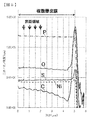
- FIG. 5 is a diagram showing the results of secondary ion mass analysis of the total element distribution in the depth direction (thickness direction) of the multilayer film of Example 1.
- FIG. 6 is the figure which expanded and displayed the result of elemental distribution of the sulfur in FIG.
- Ni and P which are main components, are almost uniformly distributed in the multi-layer film, while S, which is presumed to be derived from saccharin, is between the nickel alloy films. Peaks are observed at each interface region of In addition, with regard to C assumed to be derived from saccharin, a tendency was observed to increase from the base material to the surface of the multilayer coating, but O was distributed almost uniformly in the multilayer coating.
- the Ni concentration in the multilayer film was 96 to 97% by mass, and the P concentration was 3 to 4% by mass.
- the S concentration was 0.040% by mass in the nickel alloy film and 0.041 to 0.043% by mass in the interface region.
- the multilayer film of the film laminate of Example 1 has a fine average crystal grain size of 6.0 nm, a Ni concentration of each nickel alloy film is 96 mass% or more, and each film It was confirmed that the difference in Ni concentration between them was 1% by mass or less. Furthermore, it was confirmed that the S concentration in the interface region between two adjacent nickel alloy films is 102% or more of the S concentration contained in the nickel alloy film sandwiching the interface region.
- FIG. 7 is a diagram showing the results of secondary ion mass analysis of the total element distribution in the depth direction (thickness direction) of the nickel alloy film of Comparative Example 1.
- S and C assumed to be derived from saccharin are also distributed substantially uniformly in the nickel alloy film. Although illustration is omitted, no peak is particularly confirmed even if the elemental distribution of sulfur is expanded. This is considered to be attributable to the formation of only one layer of a 10 ⁇ m thick nickel alloy film.
- the Ni concentration in the nickel alloy film was 96 to 97 mass%, the P concentration was 3 to 4 mass%, and the S concentration was 0.040 mass%.
- Example 1 As shown in Table 3, in Example 1, the hardness was 885 HV, the corrosion resistance was 42 cycles, and the wear resistance was 4.32 m / ⁇ g. In Example 2, the hardness was 858 HV, the corrosion resistance was 42 cycles, and the wear resistance was 3.52 m / ⁇ g. In Example 3, the hardness was 849 HV, the corrosion resistance was 42 cycles, and the wear resistance was 4.08 m / ⁇ g. That is, it was confirmed that Examples 1 to 3 all show high hardness, good corrosion resistance, and good wear resistance.
- Comparative Example 1 had a hardness of 800 HV, corrosion resistance of 33 cycles, and wear resistance of 1.61 m / ⁇ g.
- Comparative Example 1 in which the nickel alloy coating 1 layer was used as the film formed on the substrate a decrease was observed in all of the hardness, the corrosion resistance, and the wear resistance as compared with Example 1.
- the cause of the corrosion resistance reduction is that the nickel alloy film is a single layer, and a sulfur concentrated layer between the alloy films is not formed. It is considered that the action did not work and pitting corrosion was likely to progress to the substrate.
- Comparative Example 2 the hardness was 617 HV, the corrosion resistance was 36 cycles, and the wear resistance was 0.88 m / ⁇ g.
- Comparative Example 2 in which the thickness of each nickel alloy film of the multilayer film was 100 nm, a decrease in hardness and abrasion resistance was particularly confirmed as compared with Example 1. The reduction in hardness and wear resistance is believed to be due to the thickness of the nickel alloy film in each layer. In other words, from the comparison with Examples 1 to 3 and Comparative Example 1, in order to obtain excellent hardness and excellent wear resistance, the thickness of the nickel alloy film in each layer may be controlled to 300 to 1000 nm. It was confirmed to be important.
- Comparative Example 3 had a hardness of 644 HV, a corrosion resistance of 40 cycles, and an abrasion resistance of 1.27 m / ⁇ g.
- the annealing temperature in the annealing step was 400 ° C.
- a decrease in hardness and wear resistance was confirmed as compared with Example 1. It is considered from the results of crystal structure analysis in Table 2 that the decrease in hardness and wear resistance is due to the coarsening of Ni phase crystal grains. In other words, in comparison with Example 1, in order to obtain excellent hardness and excellent wear resistance, it was confirmed that it is important to control the average grain size of the Ni phase to 8 nm or less. .
Landscapes
- Chemical & Material Sciences (AREA)
- Engineering & Computer Science (AREA)
- Chemical Kinetics & Catalysis (AREA)
- Electrochemistry (AREA)
- Materials Engineering (AREA)
- Metallurgy (AREA)
- Organic Chemistry (AREA)
- Crystallography & Structural Chemistry (AREA)
- Electroplating Methods And Accessories (AREA)
- Other Surface Treatments For Metallic Materials (AREA)
- Laminated Bodies (AREA)
Abstract
本発明は、環境懸念物質である6価クロムを含まず、耐食性及び耐摩耗性に優れた皮膜が基材上に積層された皮膜積層体およびその製造方法を提供することを目的とする。本発明に係る皮膜積層体は、複数層の皮膜が基材上に積層された積層体であって、前記複数層の皮膜は、複数のS含有Ni合金皮膜の層と、該複数のS含有Ni合金皮膜の層間に形成され前記S含有Ni合金皮膜のS濃度よりも高いS濃度を有する硫黄濃縮層とを有し、前記複数のS含有Ni合金皮膜の各膜は、Ni濃度が90質量%以上であり、各膜の前記Ni濃度の差が1質量%以内であることを特徴とする。
Description
本発明は、基材上に複数層の皮膜が積層された皮膜積層体及びその製造方法に関するものである。
近年、様々な機器において、以前よりも過酷環境下で使用される傾向が強まっている。例えば、洋上風力発電設備や、海水淡水化装置で用いられる配管やポンプ、融雪剤等が多量に散布される塩害が著しい地域における自動車や建設機器などが挙げられる。
そのような機器に用いられている金属部品では、腐食や摩耗などの複合的要因により金属部品表面の劣化が進行し易く、機器のメンテナンス頻度の増大、さらには機器寿命の短縮を招くことが危惧される。
現状、前述した複合的要因による劣化が進行し易い金属部品には、耐食性および耐摩耗性に優れた6価クロムめっきによる表面処理がしばしば採用されている。
しかしながら、6価クロムは、REACH規則(Regulation concerning the Registration, Evaluation, Authorization and Restriction of Chemicals, establishing a European Chemicals Agency)等の環境規制や排水規制において環境高懸念物質として指定されており、その使用削減が世界的に望まれている。そのような背景を受け、6価クロムめっきに代替するめっき技術として様々な表面処理技術が提案されている。
例えば、特許文献1には、被めっき材の表面に複数のNi合金めっき皮膜が形成され、各層Ni合金めっき皮膜がP、B、Sから選ばれる元素を異なる濃度で含有し、かつ隣接するNi合金めっき皮膜の相互の電位的関係が、外側のNi合金めっき皮膜がその内側Niめっき皮膜より30 mV以上卑なる関係をもって設けられている多層Ni合金めっき皮膜等が開示されている。
特許文献1の技術は、耐食性と生産性の向上を目的とした多層Ni合金めっき皮膜であり、層間電位差による犠牲防食作用を発現させるため、一つのめっき浴で電流密度を変えることで各層のめっき皮膜中のPなどの半金属元素の含有量を調整している。その結果、多層めっき皮膜の層ごとに硬度が異なり、多層めっき皮膜全体としての耐摩耗性は十分とは言えなかった。すなわち、皮膜の耐摩耗性に関しては更なる向上が求められている。
以上に鑑みて、本発明は、環境懸念物質である6価クロムを含まず、耐食性及び耐摩耗性に優れた皮膜が基材上に積層された皮膜積層体およびその製造方法を提供することを目的とする。
(I)本発明の一態様は、複数層の皮膜が基材上に積層された積層体であって、前記複数層の皮膜は、複数の硫黄(S)含有ニッケル(Ni)合金皮膜の層と、該複数のS含有Ni合金皮膜の層間に形成され前記S含有Ni合金皮膜のS濃度よりも高いS濃度を有する硫黄濃縮層とを有し、前記複数のS含有Ni合金皮膜の各膜は、Ni濃度が90質量%以上であり、各膜の前記Ni濃度の差が1質量%以内であることを特徴とする皮膜積層体、を提供するものである。
本発明は、上記の皮膜積層体(I)において、以下のような改良や変更を加えることができる。
(i)前記硫黄濃縮層のS濃度は、前記複数のS含有Ni合金皮膜のS濃度の102%以上である。
(ii)前記複数のS含有Ni合金皮膜の各膜は、同じ厚さを有する。
(iii)前記複数のS含有Ni合金皮膜の各膜は、厚さが300 nm以上1000 nm以下である。
(iv)前記複数のS含有Ni合金皮膜の各膜は、リン(P)を更に含有する。
(v)前記複数のS含有Ni合金皮膜の各膜は、平均結晶粒径が8 nm以下である。
(i)前記硫黄濃縮層のS濃度は、前記複数のS含有Ni合金皮膜のS濃度の102%以上である。
(ii)前記複数のS含有Ni合金皮膜の各膜は、同じ厚さを有する。
(iii)前記複数のS含有Ni合金皮膜の各膜は、厚さが300 nm以上1000 nm以下である。
(iv)前記複数のS含有Ni合金皮膜の各膜は、リン(P)を更に含有する。
(v)前記複数のS含有Ni合金皮膜の各膜は、平均結晶粒径が8 nm以下である。
(II)本発明の他の一態様は、上記の皮膜積層体の製造方法であって、複数回のニッケル合金めっき処理ステップと、アニール処理ステップとを有し、前記アニール処理ステップは、アニール温度が300℃以下であることを特徴とする積層体の製造方法、を提供するものである。
本発明は、上記の皮膜積層体の製造方法(II)において、以下のような改良や変更を加えることができる。
(vi)前記複数回のニッケル合金めっき処理ステップの間に、めっき処理停止ステップを挟む。
(vi)前記複数回のニッケル合金めっき処理ステップの間に、めっき処理停止ステップを挟む。
本発明によれば、環境懸念物質である6価クロムを含まず、耐食性及び耐摩耗性に優れた皮膜が基材上に積層された皮膜積層体およびその製造方法を提供することができる。
以下、本発明に係る実施形態について図面を参照しながら説明する。なお、本発明は、ここで取り上げた実施形態に限定されることはなく、発明の技術的思想を逸脱しない範囲で、公知技術と適宜組み合わせたり公知技術に基づいて改良したりすることが可能である。
[皮膜積層体]
図1は、本発明に係る皮膜積層体の一例を示す概略断面模式図である。図1に示したように、皮膜積層体は、基材2表面に複数層皮膜1が形成されている。ここでは、複数層皮膜1は、硫黄含有ニッケル合金皮膜3と硫黄含有ニッケル合金皮膜4との2層が積層されている。なお、以下、「硫黄含有ニッケル合金皮膜」を単純に「ニッケル合金皮膜」と称する場合がある。
図1は、本発明に係る皮膜積層体の一例を示す概略断面模式図である。図1に示したように、皮膜積層体は、基材2表面に複数層皮膜1が形成されている。ここでは、複数層皮膜1は、硫黄含有ニッケル合金皮膜3と硫黄含有ニッケル合金皮膜4との2層が積層されている。なお、以下、「硫黄含有ニッケル合金皮膜」を単純に「ニッケル合金皮膜」と称する場合がある。
複数層皮膜1を形成する基材2は、特に限定は無く、皮膜積層体の用途に応じて適宜選択できる。例えば、炭素鋼、低合金鋼、ステンレス鋼、銅、アルミニウム、それらの合金などを適宜利用できる。
本発明の皮膜積層体の特徴は、複数層皮膜1において、隣接する硫黄含有ニッケル合金皮膜3と硫黄含有ニッケル合金皮膜4との間(界面領域)に、それら硫黄含有ニッケル合金皮膜3,4のS濃度よりも高いS濃度を有する硫黄濃縮層5を備えることである。
本発明の皮膜積層体は、複数層皮膜1の皮膜間(隣接する皮膜の界面領域)に犠牲防食作用を有する硫黄濃縮層5を備えることで、従来技術では通常、膜厚方向(皮膜に垂直方向)に進行する孔食を、皮膜平行方向(皮膜に水平方向)に転換させることができ、それにより基材2に到達する腐食を抑制することができる。言い換えると、複数層皮膜1の構成層として硫黄濃縮層5を備えることにより、皮膜積層体の耐食性を向上させることが可能となる。
犠牲防食作用の観点から、硫黄濃縮層5のS濃度は、隣接する硫黄含有ニッケル合金皮膜3,4のS濃度よりも高い方が好ましく、より具体的には102%以上であることが望ましい。
また、本発明では、硫黄濃縮層5を挟持する硫黄含有ニッケル合金皮膜3,4のNi濃度は90質量%以上が好ましく、且つ硫黄含有ニッケル合金皮膜3と硫黄含有ニッケル合金皮膜4とのNi濃度差は1質量%%以内が好ましい。
このようにすることで、各硫黄含有ニッケル合金皮膜の硬度を同等に増大することができ、複数層皮膜1の摩耗速度を一様に低下させる(低速化かつ一定化する)ことができる。言い換えると、各硫黄含有ニッケル合金皮膜のNi濃度を90質量%以上とし、且つNi濃度差を1質量%以内に制御することにより、皮膜積層体の耐摩耗性を向上させることが可能となる。
ニッケル合金皮膜の硬度を増大させることを目的に、ニッケル合金の合金成分として半金属元素(例えば、リン(P)、ホウ素(B))を含有させてもよい。同様に、皮膜の硬度を増大させる目的で、酸化物(例えば、酸化チタン(TiO2)、酸化アルミニウム(Al2O3))の粒子や、炭化物(例えば、炭化ケイ素(SiC))の粒子を分散させてもよい。コスト面や生産性を考慮すると、ニッケル合金の成分としてPを含有させることが望ましい。この場合、P濃度も各ニッケル合金皮膜で同等であることが望ましい。
また、各ニッケル合金皮膜は、硬度を高める観点から(すなわち、耐摩耗性を高める観点から)、結晶粒径が小さい方が好ましく、より具体的には平均結晶粒径が4 nm以上8 nm以下が望ましく、6 nm以上8 nm以下とすることがより望ましい。
各ニッケル合金皮膜の厚さは、300 nm以上1000 nm以下とすることが好ましい。さらに、各ニッケル合金皮膜の厚さを揃える(同等とする)ことが望ましい。
図8は、同じ厚さのニッケル合金皮膜(ここではNiP層)を多層化した場合の各NiP層の厚さと複数層皮膜の硬度(ビッカース硬さ)との関係を示すグラフである。各試験試料は、NiP層間に硫黄濃縮層を有するものであり、複数層皮膜全体の厚さが約10μmとなるように層数を調整した。
図8に示したように、各ニッケル合金皮膜の厚さを300 nm以上1000 nm以下の範囲で同等にすることにより、複数層皮膜1のビッカース硬さを800 HV以上に高められることが分かる。すなわち、各合金皮膜の厚さを当該範囲に制御することにより、耐摩耗性を向上させることができる。また、各合金皮膜の厚さを統一することにより、製造制御が容易になり生産性の向上も期待できる。なお、この結果の要因については、残念ながら現段階で解明できていない。
本発明の皮膜積層体は、耐食性・耐摩耗性が要求される部品・製品に好ましく適用できる。
[皮膜積層体の製造方法]
本発明に係る皮膜積層体の製造方法について説明する。本発明の皮膜積層体の製造方法(複数層皮膜の製膜方法)としては、湿式処理(例えば、電気めっき)や乾式処理(例えば、スパッタリング)などの処理方法を利用できる。量産性の観点からは、電気めっきが好ましい形態である。
本発明に係る皮膜積層体の製造方法について説明する。本発明の皮膜積層体の製造方法(複数層皮膜の製膜方法)としては、湿式処理(例えば、電気めっき)や乾式処理(例えば、スパッタリング)などの処理方法を利用できる。量産性の観点からは、電気めっきが好ましい形態である。
複数層皮膜1を製膜するための電気めっき液は、特に限定は無く、硫酸ニッケル、塩化ニッケル、ホウ酸などを主成分とするワット浴に合金成分と硫黄含有有機化合物を添加したものを使用することができる。例えば、合金成分としてリンを用いる場合には、ホスホン酸などを添加することができる。また、硫黄含有有機化合物としては、公知の光沢剤であるサッカリン、ラウリル硫酸ナトリウム、アリルスルホン酸、チオ尿素などを使用できる。
このように、ワット浴に硫黄含有有機化合物を添加することで、ニッケル合金皮膜が硬質化・平滑化され、複数層皮膜1の耐摩耗性が向上する。なお、電気めっき液の各種成分濃度は適宜調整することができる。
図2は、本発明に係る皮膜積層体の製造方法の一例を示すフロー図であり、電気めっきプロセスを示したものである。図2に示すように、皮膜積層体の製造プロセスは、以下の順序で行われる。
1.ニッケル合金皮膜3のめっき処理ステップ
2.めっき処理停止ステップ
3.ニッケル合金皮膜4のめっき処理ステップ
4.水洗ステップ
5.乾燥ステップ
6.アニール処理ステップ。
2.めっき処理停止ステップ
3.ニッケル合金皮膜4のめっき処理ステップ
4.水洗ステップ
5.乾燥ステップ
6.アニール処理ステップ。
なお、図2においては、ニッケル合金皮膜3とニッケル合金皮膜4との2層を積層した複数層皮膜1について記載したが、皮膜積層体が適用される部品や製品に要求される耐食性、耐摩耗性、寿命などの仕様に応じて、ニッケル合金皮膜の層数は適宜設定することができる。その場合、複数層皮膜1のニッケル合金皮膜の層数に応じて、上記1~3のステップを適宜繰り返し行えばよい。
本発明の皮膜積層体の複数層皮膜1において、優れた耐食性と優れた耐摩耗性とを発現させるためには、上記プロセスにおける2.めっき処理停止ステップと6.アニール処理ステップとが重要となる。
めっき処理停止ステップでは、めっき液に浸漬したままでめっき処理の停止時間を30秒間以上とすることが好ましい。これは、本発明者等が鋭意研究した結果から得られた知見であり、硫黄含有有機化合物がニッケル合金皮膜3の表面に十分に吸着するために必要な時間である。
めっき処理停止ステップのめっき停止時間を30秒間以上とすることにより、ニッケル合金皮膜3の表面(後におけるニッケル合金皮膜3,4の界面領域)に硫黄濃縮層5を形成することができる。また、めっき停止時間により複数層皮膜1の硬度が変化することが確認されている。
図3は、めっき処理停止ステップのめっき停止時間と複数層皮膜の硬度(ビッカース硬さ)との関係例を示すグラフである。比較のため、めっき処理を停止した際に、被めっき材を直ちにめっき液から取り出して水洗した例(すなわち、めっき液に浸漬したままでのめっき停止時間が0秒間の例)も併せて示す。
図3に示したように、被めっき材をめっき液に浸漬させたままでめっき停止時間を30秒間以上とすることで複数層皮膜1のビッカース硬さが向上することが確認される。一方、めっき処理を停止した際に、被めっき材を直ちにめっき液から取り出して水洗した試料(水洗有りの試料)では、ビッカース硬さが低下することが確認される。
めっき皮膜への硫黄成分添加の作用効果として、一般的にはめっき皮膜表面の平滑化および犠牲防食作用などが知られている。これに加えて、本発明では、硫黄濃縮層5の適切な形成により、複数層皮膜1のビッカース硬さが向上するという作用効果が得られる。
この要因の1つとしては、硫黄濃縮層5の存在により、後工程のアニール処理ステップにおいてニッケル合金皮膜の結晶粒粗大化が抑制されているのではないかと考えられる。より具体的には、硫黄濃縮層5からの硫黄成分の拡散浸透により、隣り合うニッケル合金皮膜3,4の結晶粒粗大化が抑制されている可能性が考えられる。
アニール処理ステップでは、アニール温度を200℃以上300℃以下とすることが好ましい。これは、本発明者等が鋭意研究した結果から得られた知見である。アニール温度を300℃以下とすることにより、ニッケル合金皮膜の平均結晶粒径を8 nm以下に維持することができる。アニール温度が200℃未満であると、複数層皮膜1の硬度の向上が不十分となる。アニール温度が300℃超になると、ニッケル合金皮膜の結晶粒が粗大化し易くなって複数層皮膜1の硬度が低下する。アニール処理時間は、特に限定は無いが、例えば1時間以上行うと良好である。
なお、1.ニッケル合金皮膜3のめっき処理ステップおよび3.ニッケル合金皮膜4のめっき処理ステップの電解条件は、所望の皮膜厚さに応じて電流密度や処理時間を適宜調整すればよく、各皮膜の厚さを統一する観点から、同じ条件とすることが好ましい。
また、必要に応じて、1.ニッケル合金皮膜3のめっき処理ステップの前に、基材2の前処理として、脱脂、酸洗などの不純物除去ステップを行ってもよい。
以上説明したように、本発明の皮膜積層体の製造方法は、1つのめっき浴を用いて、同じ電解条件にてニッケル合金皮膜を複数層形成するため、簡便で生産性が高い(すなわち、低コストである)という利点がある。
本発明において、基材2の形状(すなわち、皮膜積層体の形状)は特に限定されず、任意の形状(例えば、塊、平板、曲板、円筒、角柱)の部品に適用できる。ただし、電気めっきにより皮膜を形成する場合は、部品形状(基材2の形状)によっては電流分布の影響で場所により皮膜厚さがばらつく可能性がある。そこで、事前に電流分布の影響を解析および実測により測定し、必要に応じて、被めっき物と対極との間に遮蔽板等を設置するなどして、めっき箇所による皮膜厚さのばらつきを抑制できる条件下で実施することが好ましい。
[皮膜積層体の変形例]
図4は、本発明に係る皮膜積層体の他の一例を示す概略断面模式図である。図4に示すように、本発明の皮膜積層体は、基材2の種類に応じて、基材2と硫黄含有ニッケル合金皮膜3との間に密着層6を設けてもよい。これは、基材2がその表面に安定な酸化皮膜などを形成する材料からなる場合に有効である。
図4は、本発明に係る皮膜積層体の他の一例を示す概略断面模式図である。図4に示すように、本発明の皮膜積層体は、基材2の種類に応じて、基材2と硫黄含有ニッケル合金皮膜3との間に密着層6を設けてもよい。これは、基材2がその表面に安定な酸化皮膜などを形成する材料からなる場合に有効である。
基材2の表面が化学的に安定な酸化皮膜で覆われていると、基材2に対する硫黄含有ニッケル合金皮膜3の密着性が弱くなり易い。そこで、基材2と硫黄含有ニッケル合金皮膜3との間に(すなわち、基材2の表面上に)密着層6を設けることにより密着性を向上させることは好ましい。例えば、ステンレス鋼などの表面が不動態化しやすい基材2の場合、ウッド浴を用いて基材2の表面上に密着層6を形成することができる。
以下、実施例により本発明の具体例をより詳細に説明する。ただし、本発明はこれらの実施例に限定されるものではない。
[実験1]
(実施例1の作製)
複数層皮膜を形成する基材として、表面を機械研磨により算術平均粗さRa=0.05μmに仕上げた鉄鋼SS400材(50 mm×70 mm×3 mm)を用いた。
(実施例1の作製)
複数層皮膜を形成する基材として、表面を機械研磨により算術平均粗さRa=0.05μmに仕上げた鉄鋼SS400材(50 mm×70 mm×3 mm)を用いた。
硫黄含有ニッケル合金皮膜の製膜には、ワット浴を基本とした表1に示す電気めっき液を用いた。ニッケル合金の対象成分はリンとし、ホスホン酸を用いた。硫黄含有有機化合物はサッカリンとした。

皮膜積層体の製造プロセスは、図2に沿って行った。具体的には、まず、基材の前処理として、脱脂・酸洗の不純物除去ステップを行った。ニッケル合金めっき処理ステップでは、各皮膜の厚さをそれぞれ500 nmとし、層数を20層(めっき処理ステップの繰返し回数を20回)とした。すなわち、複数層皮膜全体としての厚さは10μmである。めっき処理ステップの電解条件は、対極にNi板を用いて定電流で行った。めっき処理ステップ間のめっき処理停止ステップでは、停止時間を30秒間とした。アニール処理ステップでは、アニール温度を300℃とし、保持時間を2時間とした。
上記手順により、実施例1の皮膜積層体を作製した。
[実験2]
(実施例2の作製)
ニッケル合金めっき処理ステップにおいて、複数層皮膜の1層あたりのニッケル合金皮膜の厚さを300 nmとし層数を34層に変更した以外は、実験1と同様にして実施例2の皮膜積層体を作製した。複数層皮膜全体としての厚さは実施例1とほぼ同等の10.2μmである。
(実施例2の作製)
ニッケル合金めっき処理ステップにおいて、複数層皮膜の1層あたりのニッケル合金皮膜の厚さを300 nmとし層数を34層に変更した以外は、実験1と同様にして実施例2の皮膜積層体を作製した。複数層皮膜全体としての厚さは実施例1とほぼ同等の10.2μmである。
[実験3]
(実施例3の作製)
ニッケル合金めっき処理ステップにおいて、複数層皮膜の1層あたりのニッケル合金皮膜の厚さを1000 nmとし層数を10層に変更した以外は、実験1と同様にして実施例3の皮膜積層体を作製した。複数層皮膜全体としての厚さは実施例1と同様に10μmである。
(実施例3の作製)
ニッケル合金めっき処理ステップにおいて、複数層皮膜の1層あたりのニッケル合金皮膜の厚さを1000 nmとし層数を10層に変更した以外は、実験1と同様にして実施例3の皮膜積層体を作製した。複数層皮膜全体としての厚さは実施例1と同様に10μmである。
[実験4]
(比較例1の作製)
ニッケル合金めっき処理ステップにおいて、ニッケル合金皮膜の厚さを10μmとし層数を1層に変更した以外は、実験1と同様にして比較例1の皮膜積層体を作製した。基材上に形成した皮膜の厚さは実施例1と同様に10μmである。
(比較例1の作製)
ニッケル合金めっき処理ステップにおいて、ニッケル合金皮膜の厚さを10μmとし層数を1層に変更した以外は、実験1と同様にして比較例1の皮膜積層体を作製した。基材上に形成した皮膜の厚さは実施例1と同様に10μmである。
[実験5]
(比較例2の作製)
ニッケル合金めっき処理ステップにおいて、複数層皮膜の1層あたりのニッケル合金皮膜の厚さを100 nmとし層数を100層に変更した以外は、実験1と同様にして比較例2の皮膜積層体を作製した。複数層皮膜全体としての厚さは実施例1と同様に10μmである。
(比較例2の作製)
ニッケル合金めっき処理ステップにおいて、複数層皮膜の1層あたりのニッケル合金皮膜の厚さを100 nmとし層数を100層に変更した以外は、実験1と同様にして比較例2の皮膜積層体を作製した。複数層皮膜全体としての厚さは実施例1と同様に10μmである。
[実験6]
(比較例3の作製)
アニール処理ステップにおいて、アニール温度を400℃に変更した以外は、実験1と同様にして比較例3の皮膜積層体を作製した。
(比較例3の作製)
アニール処理ステップにおいて、アニール温度を400℃に変更した以外は、実験1と同様にして比較例3の皮膜積層体を作製した。
[実験7]
実施例1~3および比較例1~3の皮膜積層体について、結晶構造解析、元素分析、硬度測定、耐食性評価、耐摩耗性評価を行った。
実施例1~3および比較例1~3の皮膜積層体について、結晶構造解析、元素分析、硬度測定、耐食性評価、耐摩耗性評価を行った。
(結晶構造解析)
皮膜積層体の複数層皮膜における相の同定および結晶粒径測定は、広角X線回折(WXRD)法を用いて行った。
皮膜積層体の複数層皮膜における相の同定および結晶粒径測定は、広角X線回折(WXRD)法を用いて行った。
(元素分析)
皮膜積層体の複数層皮膜における元素分布測定は、二次イオン質量分析(SIMS)法を用いて行った。
皮膜積層体の複数層皮膜における元素分布測定は、二次イオン質量分析(SIMS)法を用いて行った。
(硬度測定)
皮膜積層体の複数層皮膜における硬度測定は、ビッカース硬度計を用いて行った。計測条件は、荷重を25 gfとし、荷重保持時間を15秒間とし、複数層皮膜の表面を測定した。
皮膜積層体の複数層皮膜における硬度測定は、ビッカース硬度計を用いて行った。計測条件は、荷重を25 gfとし、荷重保持時間を15秒間とし、複数層皮膜の表面を測定した。
(耐食性評価)
耐食性評価は、JIS K 5600-7-9「中性塩水噴霧サイクル試験法」に準拠した複合サイクル試験を行った。評価方法は、犠牲防食作用による効果を見るために、腐食開始時のサイクル数ではなく、試験片が50%以上腐食したサイクル数とした。
耐食性評価は、JIS K 5600-7-9「中性塩水噴霧サイクル試験法」に準拠した複合サイクル試験を行った。評価方法は、犠牲防食作用による効果を見るために、腐食開始時のサイクル数ではなく、試験片が50%以上腐食したサイクル数とした。
(耐摩耗性評価)
耐摩耗性評価は、往復摺動試験機を用いて行った。相手材を無潤滑の条件下で所定荷重および所定速度で往復摺動させた後、試験片の摩耗痕をレーザ顕微鏡で測定し、単位摺動距離あたりの摩耗量(μg/m)を算出し、その逆数(m/μg)を指標とした。摺動条件は、速度を0.1 m/sとし、荷重を9.8 Nとし、距離を0.04 mとし、相手材を軸受鋼SUJ2(球径10 mm)とした。
耐摩耗性評価は、往復摺動試験機を用いて行った。相手材を無潤滑の条件下で所定荷重および所定速度で往復摺動させた後、試験片の摩耗痕をレーザ顕微鏡で測定し、単位摺動距離あたりの摩耗量(μg/m)を算出し、その逆数(m/μg)を指標とした。摺動条件は、速度を0.1 m/sとし、荷重を9.8 Nとし、距離を0.04 mとし、相手材を軸受鋼SUJ2(球径10 mm)とした。
実施例1および比較例3の結晶構造解析の結果を表2に示す。

表2に示したように、実施例1では、結晶性のNi相と非結晶性のNi相とが確認され、結晶性Ni相の平均結晶粒径は6.0 nmであった。一方、比較例3では、皮膜積層体には結晶性Ni相と結晶性Ni3P相とが確認され、結晶性Ni相の平均結晶粒径は12.4 nmであった。
図5は、実施例1の複数層皮膜における深さ方向(厚さ方向)の全元素分布を二次イオン質量分析した結果を示す図である。また、図6は、図5における硫黄の元素分布の結果を拡大表示した図である。
図5~6に示したように、主成分であるNiとPとは、複数層皮膜の中でほぼ均一に分布しているのに対し、サッカリン由来と推察されるSは、ニッケル合金皮膜間の各界面領域でピークが観察される。また、サッカリン由来と推察されるCについては、基材から複数層皮膜の表面に向けて増加する傾向が見られたが、Oについては、複数層皮膜の中でほぼ均一に分布していた。
成分濃度に関しては、複数層皮膜中のNi濃度が96~97質量%であり、P濃度が3~4質量%であった。S濃度については、ニッケル合金皮膜中が0.040質量%であり、界面領域が0.041~0.043質量%であった。
結晶構造解析および元素分析から、実施例1の皮膜積層体の複数層皮膜は、平均結晶粒径が6.0 nmと微細であり、各ニッケル合金皮膜のNi濃度が96質量%以上で、かつ各皮膜間のNi濃度の差が1質量%以下であることが確認された。さらに、隣接する2層のニッケル合金皮膜間の界面領域のS濃度は、該界面領域を挟むニッケル合金皮膜が含有するS濃度の102%以上であることが確認された。
図7は、比較例1のニッケル合金皮膜における深さ方向(厚さ方向)の全元素分布を二次イオン質量分析した結果を示す図である。図7に示したように、主成分であるNiおよびPに加えて、サッカリン由来と推察されるSおよびCも、ニッケル合金皮膜中でほぼ均一に分布している。図示は省略するが、硫黄の元素分布を拡大してもピークは特に確認されなかった。これは、10μm厚さのニッケル合金皮膜を1層のみ製膜したことに起因すると考えられる。
成分濃度に関しては、ニッケル合金皮膜中のNi濃度は96~97質量%であり、P濃度は3~4質量%であり、S濃度は0.040質量%であった。
実施例1~3および比較例1~3の硬度測定、耐食性評価および耐摩耗性評価の結果を表3に示す。
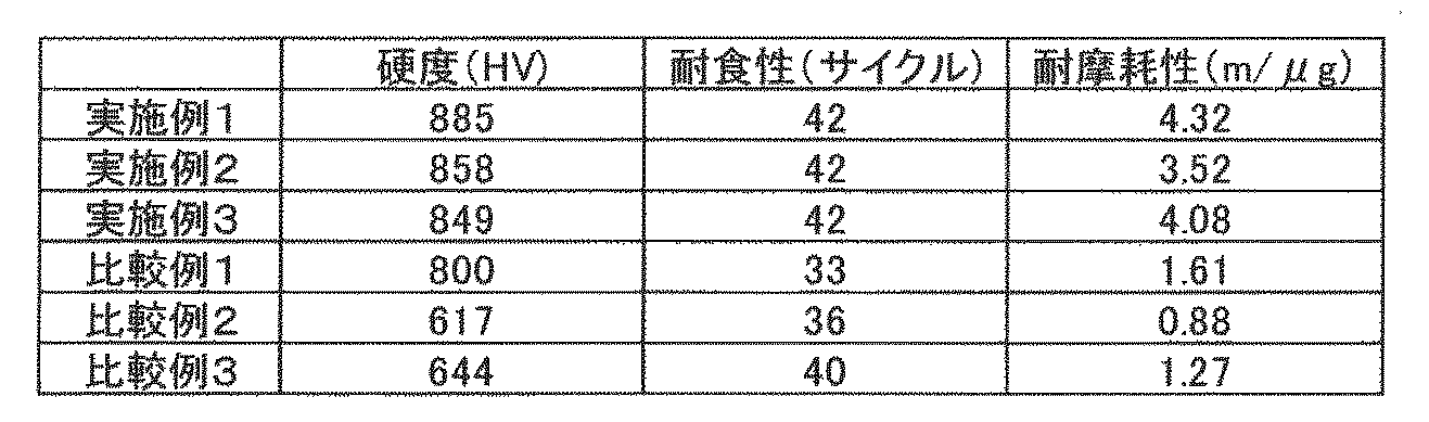
表3に示したように、実施例1では、硬度が885 HV、耐食性が42サイクル、耐摩耗性が4.32 m/μgであった。実施例2では、硬度が858 HV、耐食性が42サイクル、耐摩耗性が3.52 m/μgであった。実施例3では、硬度が849 HV、耐食性が42サイクル、耐摩耗性が4.08 m/μgであった。すなわち、実施例1~3は、いずれも高い硬度、良好な耐食性、および良好な耐摩耗性を示すことが確認された。
また、各ニッケル合金皮膜の厚さが300~1000 nmの範囲であれば、同等の特性(硬度、耐食性、耐摩耗性)を得られることが確認された。
実施例1~3に対し、比較例1は、硬度が800 HV、耐食性が33サイクル、耐摩耗性が1.61 m/μgであった。基材上に製膜する皮膜をニッケル合金皮膜1層とした比較例1は、実施例1と比較して、硬度、耐食性および耐摩耗性の全てで低下が確認された。特に、耐食性低下の原因は、図7の元素分析結果からも分かるように、ニッケル合金皮膜が単層であることから合金皮膜間の硫黄濃縮層が形成されていないことに起因して、犠牲防食作用が働かず、孔食が基材まで進行し易くなったと考えられる。
比較例2は、硬度が617 HV、耐食性が36サイクル、耐摩耗性が0.88 m/μgであった。複数層皮膜の各ニッケル合金皮膜の厚さを100 nmとした比較例2は、実施例1と比較して、特に硬度および耐摩耗性の低下が確認された。硬度および耐摩耗性の低下は、各層のニッケル合金皮膜の厚さに起因すると考えられる。言い換えると、実施例1~3および比較例1との比較から、優れた硬度および優れた耐摩耗性を得るためには、各層のニッケル合金皮膜の厚さを300~1000 nmに制御することが重要であることが確認された。
比較例3は、硬度が644 HV、耐食性が40サイクル、耐摩耗性が1.27 m/μgであった。アニール処理ステップのアニール温度を400℃とした比較例3は、実施例1と比較して、特に硬度および耐摩耗性の低下が確認された。硬度および耐摩耗性の低下は、表2の結晶構造解析の結果からNi相結晶粒の粗大化に起因すると考えられる。言い換えると、実施例1との比較から、優れた硬度および優れた耐摩耗性を得るためには、Ni相の平均結晶粒径を8 nm以下に制御することが重要であることが確認された。
上述した実施形態や実施例は、本発明の理解を助けるために説明したものであり、本発明は、記載した具体的な構成のみに限定されるものではない。例えば、実施形態の構成の一部を当業者の技術常識の構成に置き換えることが可能であり、また、実施形態の構成に当業者の技術常識の構成を加えることも可能である。すなわち、本発明は、本明細書の実施形態や実施例の構成の一部について、発明の技術的思想を逸脱しない範囲で、削除・他の構成に置換・他の構成の追加をすることが可能である。
1…複数層皮膜、2…基材、3,4…硫黄含有ニッケル合金皮膜、5…硫黄濃縮層、6…密着層。
Claims (8)
- 複数層の皮膜が基材上に積層された積層体であって、
前記複数層の皮膜は、複数の硫黄含有ニッケル合金皮膜の層と、該複数の硫黄含有ニッケル合金皮膜の層間に形成され前記硫黄含有ニッケル合金皮膜の硫黄濃度よりも高い硫黄濃度を有する硫黄濃縮層と、を有し、
前記複数の硫黄含有ニッケル合金皮膜の各膜は、ニッケル濃度が90質量%以上であり、各膜の前記ニッケル濃度の差が1質量%以内であることを特徴とする皮膜積層体。 - 請求項1に記載の皮膜積層体において、
前記硫黄濃縮層の硫黄濃度は、前記複数の硫黄含有ニッケル合金皮膜の硫黄濃度の102%以上であることを特徴とする皮膜積層体。 - 請求項1又は請求項2に記載の皮膜積層体において、
前記複数の硫黄含有ニッケル合金皮膜の各膜は、同じ厚さを有することを特徴とする皮膜積層体。 - 請求項1乃至請求項3のいずれか一項に記載の皮膜積層体において、
前記複数の硫黄含有ニッケル合金皮膜の各膜は、厚さが300 nm以上1000 nm以下であることを特徴とする皮膜積層体。 - 請求項1乃至請求項4のいずれか一項に記載の皮膜積層体において、
前記複数の硫黄含有ニッケル合金皮膜の各膜は、リンを更に含有することを特徴とする皮膜積層体。 - 請求項1乃至請求項5のいずれか一項に記載の皮膜積層体において、
前記複数の硫黄含有ニッケル合金皮膜の各膜は、平均結晶粒径が8 nm以下であることを特徴とする皮膜積層体。 - 請求項1に記載の皮膜積層体の製造方法であって、
複数回のニッケル合金めっき処理ステップと、アニール処理ステップと、を有し、
前記アニール処理ステップは、アニール温度が300℃以下であることを特徴とする皮膜積層体の製造方法。 - 請求項7に記載の皮膜積層体の製造方法であって、
前記複数回のニッケル合金めっき処理ステップの間に、めっき処理停止ステップを挟むことを特徴とする皮膜積層体の製造方法。
Priority Applications (3)
| Application Number | Priority Date | Filing Date | Title |
|---|---|---|---|
| CN201880062178.5A CN111133132B (zh) | 2017-09-27 | 2018-05-08 | 被膜层叠体及其制造方法 |
| US16/650,626 US11279112B2 (en) | 2017-09-27 | 2018-05-08 | Coating laminated body and method for producing the same |
| JP2019544232A JP6813692B2 (ja) | 2017-09-27 | 2018-05-08 | 皮膜積層体及びその製造方法 |
Applications Claiming Priority (2)
| Application Number | Priority Date | Filing Date | Title |
|---|---|---|---|
| JP2017185614 | 2017-09-27 | ||
| JP2017-185614 | 2017-09-27 |
Publications (1)
| Publication Number | Publication Date |
|---|---|
| WO2019064672A1 true WO2019064672A1 (ja) | 2019-04-04 |
Family
ID=65901529
Family Applications (1)
| Application Number | Title | Priority Date | Filing Date |
|---|---|---|---|
| PCT/JP2018/017692 Ceased WO2019064672A1 (ja) | 2017-09-27 | 2018-05-08 | 皮膜積層体及びその製造方法 |
Country Status (4)
| Country | Link |
|---|---|
| US (1) | US11279112B2 (ja) |
| JP (1) | JP6813692B2 (ja) |
| CN (1) | CN111133132B (ja) |
| WO (1) | WO2019064672A1 (ja) |
Cited By (1)
| Publication number | Priority date | Publication date | Assignee | Title |
|---|---|---|---|---|
| WO2021199468A1 (ja) | 2020-03-31 | 2021-10-07 | 株式会社日立製作所 | 積層体、金属めっき液、および積層体の製造方法 |
Citations (5)
| Publication number | Priority date | Publication date | Assignee | Title |
|---|---|---|---|---|
| JPS5950195A (ja) * | 1982-09-14 | 1984-03-23 | Toagosei Chem Ind Co Ltd | 陰極の再生法 |
| JPS63105990A (ja) * | 1986-10-23 | 1988-05-11 | Kawasaki Steel Corp | 多層ニツケル合金めつきおよびその形成方法 |
| JPH06200382A (ja) * | 1992-12-29 | 1994-07-19 | Inax Corp | 耐食性に優れた水栓金具 |
| JP2001279489A (ja) * | 2000-03-30 | 2001-10-10 | Dowa Mining Co Ltd | 電気接触材料及びその製造方法 |
| WO2006043507A1 (ja) * | 2004-10-18 | 2006-04-27 | Yamaha Hatsudoki Kabushiki Kaisha | エンジン用部品 |
Family Cites Families (9)
| Publication number | Priority date | Publication date | Assignee | Title |
|---|---|---|---|---|
| JP3045612B2 (ja) * | 1992-06-22 | 2000-05-29 | 東洋鋼鈑株式会社 | 高耐食性ニッケルめっき鋼帯およびその製造法 |
| JP3918142B2 (ja) * | 1998-11-06 | 2007-05-23 | 株式会社日立製作所 | クロムめっき部品、クロムめっき方法およびクロムめっき部品の製造方法 |
| CN1389598A (zh) * | 2002-07-07 | 2003-01-08 | 余泽玲 | 一种低温低浓度纳米复合镍多层组合的电镀方法 |
| JP4362599B2 (ja) * | 2004-03-05 | 2009-11-11 | Dowaメタルテック株式会社 | 金属部材およびそれを用いた電気接点 |
| US10266957B2 (en) * | 2009-02-13 | 2019-04-23 | Nissan Motor Co., Ltd. | Chrome-plated part and manufacturing method of the same |
| CN101550576B (zh) * | 2009-04-17 | 2011-05-18 | 昆明理工大学 | 一种锌镍合金纳米多层膜 |
| CN101988211A (zh) * | 2009-08-06 | 2011-03-23 | 江苏振宇汽车部件有限公司 | 一种具有优良防腐性能的金属表面多层镀镍工艺 |
| US10752999B2 (en) * | 2016-04-18 | 2020-08-25 | Rolls-Royce Corporation | High strength aerospace components |
| CN108396348B (zh) * | 2018-03-30 | 2020-01-21 | 芜湖强振汽车紧固件有限公司 | 一种紧固件的电镀层、电镀液及电镀工艺 |
-
2018
- 2018-05-08 US US16/650,626 patent/US11279112B2/en active Active
- 2018-05-08 JP JP2019544232A patent/JP6813692B2/ja active Active
- 2018-05-08 WO PCT/JP2018/017692 patent/WO2019064672A1/ja not_active Ceased
- 2018-05-08 CN CN201880062178.5A patent/CN111133132B/zh active Active
Patent Citations (5)
| Publication number | Priority date | Publication date | Assignee | Title |
|---|---|---|---|---|
| JPS5950195A (ja) * | 1982-09-14 | 1984-03-23 | Toagosei Chem Ind Co Ltd | 陰極の再生法 |
| JPS63105990A (ja) * | 1986-10-23 | 1988-05-11 | Kawasaki Steel Corp | 多層ニツケル合金めつきおよびその形成方法 |
| JPH06200382A (ja) * | 1992-12-29 | 1994-07-19 | Inax Corp | 耐食性に優れた水栓金具 |
| JP2001279489A (ja) * | 2000-03-30 | 2001-10-10 | Dowa Mining Co Ltd | 電気接触材料及びその製造方法 |
| WO2006043507A1 (ja) * | 2004-10-18 | 2006-04-27 | Yamaha Hatsudoki Kabushiki Kaisha | エンジン用部品 |
Cited By (5)
| Publication number | Priority date | Publication date | Assignee | Title |
|---|---|---|---|---|
| WO2021199468A1 (ja) | 2020-03-31 | 2021-10-07 | 株式会社日立製作所 | 積層体、金属めっき液、および積層体の製造方法 |
| JP2021160117A (ja) * | 2020-03-31 | 2021-10-11 | 株式会社日立製作所 | 積層体、金属めっき液、および積層体の製造方法 |
| EP4130346A4 (en) * | 2020-03-31 | 2023-12-20 | Hitachi, Ltd. | Laminate, metal plating liquid, and laminate manufacturing method |
| JP7520550B2 (ja) | 2020-03-31 | 2024-07-23 | 株式会社日立製作所 | 積層体、金属めっき液、および積層体の製造方法 |
| US12371792B2 (en) | 2020-03-31 | 2025-07-29 | Hitachi, Ltd. | Laminate, metal plating solution, and manufacturing process of laminate |
Also Published As
| Publication number | Publication date |
|---|---|
| US20200255965A1 (en) | 2020-08-13 |
| JPWO2019064672A1 (ja) | 2020-04-02 |
| US11279112B2 (en) | 2022-03-22 |
| CN111133132B (zh) | 2022-06-28 |
| JP6813692B2 (ja) | 2021-01-13 |
| CN111133132A (zh) | 2020-05-08 |
Similar Documents
| Publication | Publication Date | Title |
|---|---|---|
| US20240410072A1 (en) | Processes for producing coated surfaces, coatings and articles using them | |
| Lu et al. | The effect of formic acid concentration on the conductivity and corrosion resistance of chromium carbide coatings electroplated with trivalent chromium | |
| Wang et al. | A novel electrodeposited Ni–P gradient deposit for replacement of conventional hard chromium | |
| CN107531017B (zh) | 具有耐腐蚀被膜的层叠体及其制造方法 | |
| Mahdavi et al. | Characteristics and properties of Cr coatings electrodeposited from Cr (III) baths | |
| Huang et al. | Corrosion resistance and formation analysis of a molybdate conversion coating prepared by alkaline treatment on aluminum alloy 6063 | |
| Jiang et al. | Erosion-corrosion behavior of electroless Ni-P coating on copper-nickel alloy in 3.5 wt.% sodium chloride solution | |
| ES2080335T5 (es) | Componente de acero con capa anticorrosiva aplicada galvanicamente. | |
| Jeong et al. | Sodium phosphate post-treatment on Al coating: Morphological and corrosion study | |
| Singh et al. | Establishing environment friendly surface treatment for AZ91 magnesium alloy for subsequent electroless nickel plating | |
| JP4542134B2 (ja) | 構造化硬質クロム層の製造およびコーティングの製造 | |
| JP6813692B2 (ja) | 皮膜積層体及びその製造方法 | |
| López et al. | Hardness and corrosion resistance of Ni/NiB Bi-layer and Ni/NiB/NiB-PTFE Tri-layer coatings prepared by electrodeposition and dynamic chemical Plating (DCP) techniques | |
| Riyadi et al. | Hardness and wear properties of laminated Cr-Ni coatings formed by electroplating | |
| Rashmi et al. | Development of nanocrystalline multilayer Ni–Fe alloy coatings: characterization and its corrosion behaviour at elevated temperature | |
| Wen et al. | Salt spray corrosion and electrochemical corrosion characteristics of CAIP and LTPN fabricated AlCrN/NL composite coating | |
| CN118176328A (zh) | 生产涂覆表面、涂层和使用它们的制品的方法 | |
| Riyadi | Mechanical properties of cu surface in the laminated structure of Cr-Cu coatings | |
| US20260126255A1 (en) | Weapons and weapon components including surface coatings | |
| Liao et al. | Corrosion and wear resistance of electroplating trivalent chromium-carbon coating | |
| Chen et al. | Influence of duty cycle on behaviors: wear, corrosion and tribocorrosion resistance of Ni-P coatings | |
| WO2024130228A1 (en) | Weapons and weapon components including surface coatings | |
| Shi et al. | Research on wear and corrosion resistance properties of various coatings for railway steel | |
| Vinogradov et al. | The influence of polishing of a composite coating on its electrochemical behavior in a corrosive medium | |
| RU2311493C1 (ru) | Цинкохроматное покрытие на стали (варианты) |
Legal Events
| Date | Code | Title | Description |
|---|---|---|---|
| 121 | Ep: the epo has been informed by wipo that ep was designated in this application |
Ref document number: 18862200 Country of ref document: EP Kind code of ref document: A1 |
|
| ENP | Entry into the national phase |
Ref document number: 2019544232 Country of ref document: JP Kind code of ref document: A |
|
| NENP | Non-entry into the national phase |
Ref country code: DE |
|
| 122 | Ep: pct application non-entry in european phase |
Ref document number: 18862200 Country of ref document: EP Kind code of ref document: A1 |