WO2019054334A1 - 高周波回路用積層体及びその製造方法、並びにbステージシート - Google Patents
高周波回路用積層体及びその製造方法、並びにbステージシート Download PDFInfo
- Publication number
- WO2019054334A1 WO2019054334A1 PCT/JP2018/033477 JP2018033477W WO2019054334A1 WO 2019054334 A1 WO2019054334 A1 WO 2019054334A1 JP 2018033477 W JP2018033477 W JP 2018033477W WO 2019054334 A1 WO2019054334 A1 WO 2019054334A1
- Authority
- WO
- WIPO (PCT)
- Prior art keywords
- resin layer
- laminate
- high frequency
- layer
- frequency circuit
- Prior art date
Links
Images


Classifications
-
- H—ELECTRICITY
- H05—ELECTRIC TECHNIQUES NOT OTHERWISE PROVIDED FOR
- H05K—PRINTED CIRCUITS; CASINGS OR CONSTRUCTIONAL DETAILS OF ELECTRIC APPARATUS; MANUFACTURE OF ASSEMBLAGES OF ELECTRICAL COMPONENTS
- H05K1/00—Printed circuits
- H05K1/02—Details
- H05K1/11—Printed elements for providing electric connections to or between printed circuits
- H05K1/118—Printed elements for providing electric connections to or between printed circuits specially for flexible printed circuits, e.g. using folded portions
-
- B—PERFORMING OPERATIONS; TRANSPORTING
- B32—LAYERED PRODUCTS
- B32B—LAYERED PRODUCTS, i.e. PRODUCTS BUILT-UP OF STRATA OF FLAT OR NON-FLAT, e.g. CELLULAR OR HONEYCOMB, FORM
- B32B27/00—Layered products comprising a layer of synthetic resin
- B32B27/38—Layered products comprising a layer of synthetic resin comprising epoxy resins
-
- B—PERFORMING OPERATIONS; TRANSPORTING
- B32—LAYERED PRODUCTS
- B32B—LAYERED PRODUCTS, i.e. PRODUCTS BUILT-UP OF STRATA OF FLAT OR NON-FLAT, e.g. CELLULAR OR HONEYCOMB, FORM
- B32B15/00—Layered products comprising a layer of metal
- B32B15/04—Layered products comprising a layer of metal comprising metal as the main or only constituent of a layer, which is next to another layer of the same or of a different material
- B32B15/08—Layered products comprising a layer of metal comprising metal as the main or only constituent of a layer, which is next to another layer of the same or of a different material of synthetic resin
- B32B15/092—Layered products comprising a layer of metal comprising metal as the main or only constituent of a layer, which is next to another layer of the same or of a different material of synthetic resin comprising epoxy resins
-
- B—PERFORMING OPERATIONS; TRANSPORTING
- B32—LAYERED PRODUCTS
- B32B—LAYERED PRODUCTS, i.e. PRODUCTS BUILT-UP OF STRATA OF FLAT OR NON-FLAT, e.g. CELLULAR OR HONEYCOMB, FORM
- B32B15/00—Layered products comprising a layer of metal
- B32B15/20—Layered products comprising a layer of metal comprising aluminium or copper
-
- B—PERFORMING OPERATIONS; TRANSPORTING
- B32—LAYERED PRODUCTS
- B32B—LAYERED PRODUCTS, i.e. PRODUCTS BUILT-UP OF STRATA OF FLAT OR NON-FLAT, e.g. CELLULAR OR HONEYCOMB, FORM
- B32B27/00—Layered products comprising a layer of synthetic resin
- B32B27/18—Layered products comprising a layer of synthetic resin characterised by the use of special additives
- B32B27/26—Layered products comprising a layer of synthetic resin characterised by the use of special additives using curing agents
-
- B—PERFORMING OPERATIONS; TRANSPORTING
- B32—LAYERED PRODUCTS
- B32B—LAYERED PRODUCTS, i.e. PRODUCTS BUILT-UP OF STRATA OF FLAT OR NON-FLAT, e.g. CELLULAR OR HONEYCOMB, FORM
- B32B27/00—Layered products comprising a layer of synthetic resin
- B32B27/28—Layered products comprising a layer of synthetic resin comprising synthetic resins not wholly covered by any one of the sub-groups B32B27/30 - B32B27/42
- B32B27/281—Layered products comprising a layer of synthetic resin comprising synthetic resins not wholly covered by any one of the sub-groups B32B27/30 - B32B27/42 comprising polyimides
-
- B—PERFORMING OPERATIONS; TRANSPORTING
- B32—LAYERED PRODUCTS
- B32B—LAYERED PRODUCTS, i.e. PRODUCTS BUILT-UP OF STRATA OF FLAT OR NON-FLAT, e.g. CELLULAR OR HONEYCOMB, FORM
- B32B27/00—Layered products comprising a layer of synthetic resin
- B32B27/36—Layered products comprising a layer of synthetic resin comprising polyesters
-
- B—PERFORMING OPERATIONS; TRANSPORTING
- B32—LAYERED PRODUCTS
- B32B—LAYERED PRODUCTS, i.e. PRODUCTS BUILT-UP OF STRATA OF FLAT OR NON-FLAT, e.g. CELLULAR OR HONEYCOMB, FORM
- B32B37/00—Methods or apparatus for laminating, e.g. by curing or by ultrasonic bonding
- B32B37/06—Methods or apparatus for laminating, e.g. by curing or by ultrasonic bonding characterised by the heating method
-
- H—ELECTRICITY
- H05—ELECTRIC TECHNIQUES NOT OTHERWISE PROVIDED FOR
- H05K—PRINTED CIRCUITS; CASINGS OR CONSTRUCTIONAL DETAILS OF ELECTRIC APPARATUS; MANUFACTURE OF ASSEMBLAGES OF ELECTRICAL COMPONENTS
- H05K1/00—Printed circuits
- H05K1/02—Details
- H05K1/0213—Electrical arrangements not otherwise provided for
- H05K1/0237—High frequency adaptations
-
- H—ELECTRICITY
- H05—ELECTRIC TECHNIQUES NOT OTHERWISE PROVIDED FOR
- H05K—PRINTED CIRCUITS; CASINGS OR CONSTRUCTIONAL DETAILS OF ELECTRIC APPARATUS; MANUFACTURE OF ASSEMBLAGES OF ELECTRICAL COMPONENTS
- H05K1/00—Printed circuits
- H05K1/02—Details
- H05K1/03—Use of materials for the substrate
-
- H—ELECTRICITY
- H05—ELECTRIC TECHNIQUES NOT OTHERWISE PROVIDED FOR
- H05K—PRINTED CIRCUITS; CASINGS OR CONSTRUCTIONAL DETAILS OF ELECTRIC APPARATUS; MANUFACTURE OF ASSEMBLAGES OF ELECTRICAL COMPONENTS
- H05K1/00—Printed circuits
- H05K1/02—Details
- H05K1/03—Use of materials for the substrate
- H05K1/0313—Organic insulating material
-
- B—PERFORMING OPERATIONS; TRANSPORTING
- B32—LAYERED PRODUCTS
- B32B—LAYERED PRODUCTS, i.e. PRODUCTS BUILT-UP OF STRATA OF FLAT OR NON-FLAT, e.g. CELLULAR OR HONEYCOMB, FORM
- B32B2250/00—Layers arrangement
- B32B2250/02—2 layers
-
- B—PERFORMING OPERATIONS; TRANSPORTING
- B32—LAYERED PRODUCTS
- B32B—LAYERED PRODUCTS, i.e. PRODUCTS BUILT-UP OF STRATA OF FLAT OR NON-FLAT, e.g. CELLULAR OR HONEYCOMB, FORM
- B32B2250/00—Layers arrangement
- B32B2250/03—3 layers
-
- B—PERFORMING OPERATIONS; TRANSPORTING
- B32—LAYERED PRODUCTS
- B32B—LAYERED PRODUCTS, i.e. PRODUCTS BUILT-UP OF STRATA OF FLAT OR NON-FLAT, e.g. CELLULAR OR HONEYCOMB, FORM
- B32B2250/00—Layers arrangement
- B32B2250/40—Symmetrical or sandwich layers, e.g. ABA, ABCBA, ABCCBA
-
- B—PERFORMING OPERATIONS; TRANSPORTING
- B32—LAYERED PRODUCTS
- B32B—LAYERED PRODUCTS, i.e. PRODUCTS BUILT-UP OF STRATA OF FLAT OR NON-FLAT, e.g. CELLULAR OR HONEYCOMB, FORM
- B32B2307/00—Properties of the layers or laminate
- B32B2307/20—Properties of the layers or laminate having particular electrical or magnetic properties, e.g. piezoelectric
- B32B2307/204—Di-electric
-
- B—PERFORMING OPERATIONS; TRANSPORTING
- B32—LAYERED PRODUCTS
- B32B—LAYERED PRODUCTS, i.e. PRODUCTS BUILT-UP OF STRATA OF FLAT OR NON-FLAT, e.g. CELLULAR OR HONEYCOMB, FORM
- B32B2307/00—Properties of the layers or laminate
- B32B2307/50—Properties of the layers or laminate having particular mechanical properties
- B32B2307/538—Roughness
-
- B—PERFORMING OPERATIONS; TRANSPORTING
- B32—LAYERED PRODUCTS
- B32B—LAYERED PRODUCTS, i.e. PRODUCTS BUILT-UP OF STRATA OF FLAT OR NON-FLAT, e.g. CELLULAR OR HONEYCOMB, FORM
- B32B2307/00—Properties of the layers or laminate
- B32B2307/50—Properties of the layers or laminate having particular mechanical properties
- B32B2307/54—Yield strength; Tensile strength
-
- B—PERFORMING OPERATIONS; TRANSPORTING
- B32—LAYERED PRODUCTS
- B32B—LAYERED PRODUCTS, i.e. PRODUCTS BUILT-UP OF STRATA OF FLAT OR NON-FLAT, e.g. CELLULAR OR HONEYCOMB, FORM
- B32B2307/00—Properties of the layers or laminate
- B32B2307/70—Other properties
- B32B2307/732—Dimensional properties
-
- B—PERFORMING OPERATIONS; TRANSPORTING
- B32—LAYERED PRODUCTS
- B32B—LAYERED PRODUCTS, i.e. PRODUCTS BUILT-UP OF STRATA OF FLAT OR NON-FLAT, e.g. CELLULAR OR HONEYCOMB, FORM
- B32B2457/00—Electrical equipment
- B32B2457/08—PCBs, i.e. printed circuit boards
Definitions
- the present invention relates to a laminate for a high frequency circuit formed by bonding a resin layer and a metal layer, a method of manufacturing the same, and a B-stage sheet.
- the present invention also relates to a laminated body wound body suitably used as a high frequency circuit board.
- a flexible printed circuit board (hereinafter also referred to as "FPC") and a flexible flat cable (hereinafter also referred to as "FFC”) are used in electronic and electrical devices.
- FPC a copper clad laminate (CCL) composed of an insulator layer and a copper foil layer is processed to form an electrical circuit, and then a cover lay comprising an insulating layer and an adhesive layer for protecting the circuit portion It manufactures through the process of attaching the adhesive part of CL) to a circuit part.
- FFC is obtained by arranging and bonding a plurality of conductors between the adhesive portions of the substrate using conductors such as a copper foil formed in a wiring shape and a substrate comprising an insulator layer and an adhesive layer. Electrical circuit.
- the adhesive layer is degraded due to an external factor (for example, storage environment) There is a problem that curling tends to occur when it is pulled out because it hardens.
- the present invention has been made in view of the above situation, and an object of the present invention is to provide a laminate for a high frequency circuit which can reduce a transmission loss of an electric signal in the high frequency circuit and can manufacture a circuit board excellent in smoothness. . Another object of the present invention is to provide a method for producing a laminate for a high frequency circuit, which can be manufactured by bonding at a low temperature and is excellent in adhesion between a resin layer and a metal layer.
- the present invention has been made to solve at least a part of the problems described above, and can be realized as the following aspects or application examples.
- One aspect of the laminate for a high frequency circuit according to the present invention is The metal layer and the resin layer are laminated in contact with each other,
- the elastic modulus of the resin layer is 0.1 to 3 GPa, It is characterized in that the dielectric loss tangent at a frequency of 10 GHz of the resin layer at 23 ° C. is 0.001 to 0.01, and the relative dielectric constant is 2 to 3.
- the peel strength between the resin layer and the metal layer may be 5 N / cm or more.
- the thickness of the resin layer may be 10 to 100 ⁇ m, and the thickness of the metal layer may be 10 to 50 ⁇ m.
- the thickness can be 50 to 200 ⁇ m.
- Application Example 5 One aspect of the flexible printed circuit according to the present invention is A laminate for a high frequency circuit according to any one of application examples 1 to 4 is provided.
- Application Example 6 One aspect of the laminate winding body according to the present invention is The laminate for a high frequency circuit according to any one of application examples 1 to 4 is formed by winding a core having a radius of 10 to 100 mm.
- a B-stage resin layer with a surface roughness Ra of 1 to 100 nm and a metal layer with a surface roughness Ra of 10 to 300 nm are heated to 50 to 200 ° C. and attached with a line load of 1 to 19 kN / m. It is characterized by including a process.
- One aspect of the B-stage sheet according to the present invention is A B-stage sheet having a B-stage resin layer and a release layer formed on at least one surface of the B-stage resin layer,
- the elastic modulus of the C-stage resin layer is 0.1 to 3 GPa
- the dielectric loss tangent at a frequency of 10 GHz at 23 ° C. of the C-stage resin layer is 0.001 to 0.01, and the relative dielectric constant is 2 to 3.
- the transmission loss of the electric signal in a high frequency circuit can be reduced, and the circuit board excellent in smoothness can be manufactured.
- manufacturing by bonding at a low temperature is possible, and a laminate for a high frequency circuit having excellent adhesion between a resin layer and a metal layer can be manufactured. it can.
- the laminated body wound body according to the present invention even when the laminated body for a high frequency circuit capable of reducing the transmission loss of the high frequency signal is wound and stored on the winding core, the wound winding is effective. Can be suppressed.
- FIG. 1A is a cross-sectional view schematically showing a step A1 in a manufacturing example A of a laminate for a high frequency circuit.
- FIG. 1B is a cross sectional view schematically showing a step A2 in a manufacturing example A of the laminate for a high frequency circuit.
- FIG. 1C is a cross-sectional view schematically showing a step A3 in a manufacturing example A of the laminate for a high frequency circuit.
- FIG. 1D is a cross sectional view schematically showing a step A4 in a manufacturing example A of the laminate for a high frequency circuit.
- FIG. 2A is a cross sectional view schematically showing a process B1 in a manufacturing example B of the laminate for a high frequency circuit.
- FIG. 2B is a cross sectional view schematically showing a step B2 in a manufacturing example B of the laminate for a high frequency circuit.
- FIG. 2C is a cross sectional view schematically showing a step B3 in a manufacturing example B of the laminate for a high frequency circuit.
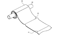
- FIG. 3 is a perspective view which shows an example of the laminated body winding body which concerns on this embodiment.
- FIG. 4 is a perspective view showing an example of a core.
- FIG. 5 is a perspective view showing a state of a pressing mark generated when the laminate is unwound from the conventional laminate winding body.
- Laminates for High Frequency Circuits The terms used in the present specification are defined as follows. "High frequency signal” means an electric signal or radio wave of a frequency of 10 GHz or more. -"Laminate for high frequency circuits” means a laminate for use in manufacturing a high frequency circuit driven at a frequency of 10 GHz or more. -"B-stage resin layer” means a layer in a state where the resin is semi-cured. -"C-stage resin layer” refers to a layer in which the resin is completely cured. In the present invention, “C-stage resin layer” may be simply referred to as “resin layer”.
- the “wound body” refers to a laminate of a uniform width high frequency circuit wound on a winding core by a predetermined length. The winding length and width are not particularly limited, but the winding length is usually 0.5 to 100 m and the width is about several tens to 1000 mm.
- the laminate for a high frequency circuit is formed by laminating a metal layer and a resin layer in contact with each other, and an adhesive layer such as a primer resin layer is not interposed between the metal layer and the resin layer.
- an adhesive layer is interposed between the resin layer and the metal layer in order to improve the adhesion between the metal layer having the conductive function and the resin layer having the insulating function.
- the adhesive layer is formed by a method such as application using an adhesive containing a polymer having mainly a polar functional group.
- an adhesive layer has poor electrical characteristics, the effective dielectric constant and the effective dielectric loss of the resin layer which bears the insulating function become large, which is unsuitable for a high frequency circuit.
- the adhesion between the metal layer and the resin layer is good even without using an adhesive, and the metal layer and the resin layer are laminated in contact with each other.
- the peel strength between the resin layer and the metal layer is preferably 5 N / cm or more, more preferably 5.3 N / cm or more, and preferably 6 N / cm or more. Is particularly preferred. Since the laminate for a high frequency circuit used in the present embodiment has the peel strength in the above range, the adhesion between the metal layer and the resin layer is good even without using an adhesive.
- the peel strength can be measured according to the method described in “IPC-TM-650 2.4.9”.
- the thickness of the laminate for a high frequency circuit used in the present embodiment is preferably 50 to 200 ⁇ m, more preferably 60 to 180 ⁇ m, and particularly preferably 70 to 150 ⁇ m.
- the thickness of the laminate for a high frequency circuit is within the above range, not only can a thinned high frequency circuit substrate be manufactured, but it becomes difficult to have a curl when wound around a winding core.
- the thickness of the laminate for a high frequency circuit is particularly preferably the height ( ⁇ m) ⁇ 10 ⁇ m of the step portion when the step portion is formed on the winding core.
- the laminate for a high frequency circuit according to the present embodiment includes a resin layer.
- the elastic modulus of the resin layer is 0.1 to 3 GPa, preferably 0.2 to 2.5 GPa. When the elastic modulus of the resin layer is in the above range, a laminate for a high frequency circuit having excellent flexibility is obtained, so that the circuit board can be manufactured under more free conditions.
- the elastic modulus of the resin layer is a tensile elastic modulus and can be measured according to JIS K 7161.
- the relative dielectric constant of the resin layer at a frequency of 10 GHz at 23 ° C. is 2 to 3, and preferably 2.1 to 2.8.
- the dielectric loss tangent at 23 ° C. and a frequency of 10 GHz of the resin layer is 0.001 to 0.01, and preferably 0.002 to 0.009.
- the circuit board excellent in the high frequency characteristic can be manufactured as a dielectric constant and a dielectric loss tangent being the said range.
- the relative dielectric constant and dielectric loss tangent of the resin layer at a frequency of 10 GHz at 23 ° C. can be measured using a cavity resonator perturbation method dielectric constant measurement apparatus.
- the thickness of the resin layer is preferably 10 to 100 ⁇ m, more preferably 20 to 90 ⁇ m, and particularly preferably 25 to 80 ⁇ m.
- the resin layer also includes an embodiment in which the resin layer is composed of a plurality of different resin layers.
- the elastic modulus, relative permittivity, and dielectric loss tangent of each resin single layer do not necessarily have to be limited to the preferable ranges described above, and the entire ranges become preferable ranges. Just do it.
- the method for producing such a resin layer is not particularly limited, but the composition for a resin layer is applied to a substrate such as a release layer or a metal foil, or is produced by a method such as extrusion molding to prepare a free standing film. can do.
- composition of the composition for resin layer is not particularly limited as long as the resin layer to be obtained has a composition that satisfies the elastic modulus, the dielectric loss tangent and the relative dielectric constant, but a polymer, a curable compound, It is preferable to contain a curing aid and a solvent.
- composition for resin layer ⁇ polymer>
- known materials having low dielectric constant and low dielectric loss tangent characteristics such as epoxy resin, polyimide, polyarylene, etc. can be used appropriately, but in particular, A polymer having a repeating unit represented by at least one of the following formulas (1-1), (1-2) and (1-3) can be preferably used.
- R 1 is each independently a halogen atom, a monovalent hydrocarbon group having 1 to 20 carbon atoms, or a monovalent halogen having 1 to 20 carbon atoms And salts of a modified hydrocarbon group, a nitro group, a cyano group, a primary to tertiary amino group, or a primary to tertiary amino group.
- Each n is independently an integer of 0 to 2. When n is 2, plural R 1 s may be the same or different and may be combined in any combination to form a part of a ring structure.
- a halogen atom a monovalent hydrocarbon group having 1 to 6 carbon atoms, a monovalent halogenated hydrocarbon group having 1 to 6 carbon atoms, a nitro group, a cyano group, a primary to tertiary amino group, or Salts of primary to tertiary amino groups are preferable, and fluorine atom, chlorine atom, methyl group, nitro group, cyano group, t-butyl group, phenyl group and amino group are more preferable.
- n 0 or 1 is preferable, and 0 is more preferable.
- the position of the other bond to one bond of the repeating unit is not particularly limited, but the meta position is preferable from the viewpoint of improving the polymerization reactivity of the monomer giving the repeating unit.
- a structural unit represented by the above formula (1-2) having a pyrimidine skeleton is preferable.
- the polymer may have a repeating unit other than the repeating unit represented by at least one of the above formulas (1-1), (1-2) and (1-3), if necessary.
- the content of the repeating unit represented by at least one of the above formulas (1-1), (1-2) and (1-3) in the polymer is 100% of the total of all structural units in the polymer.
- mol% it is preferably 5 to 95 mol%, and more preferably 10 to 60 mol%.
- the synthesis method of the polymer having a repeating unit represented by at least one of the above formulas (1-1), (1-2) and (1-3) is not particularly limited, and a known method may be used.
- a monomer giving a repeating unit represented by at least one of the above formulas (1-1), (1-2) and (1-3) and, if necessary, other monomers Can be synthesized by heating with an alkali metal or the like in an organic solvent.
- the lower limit of the weight average molecular weight (Mw) of the polymer having a repeating unit represented by at least one of the above formulas (1-1), (1-2) and (1-3) is 500 Is preferred, 1,000 is more preferred, 10,000 is even more preferred, 30,000 is particularly preferred.
- the upper limit of the weight average molecular weight (Mw) is preferably 600,000, more preferably 400,000, still more preferably 300,000, and particularly preferably 200,000.
- the lower limit of the glass transition temperature (Tg) of the polymer having a repeating unit represented by at least one of the above formulas (1-1), (1-2) and (1-3) is preferably 150 ° C. And 180 ° C. are more preferable. 320 degreeC is preferable and, as for the upper limit of a glass transition temperature (Tg), 300 degreeC is more preferable.
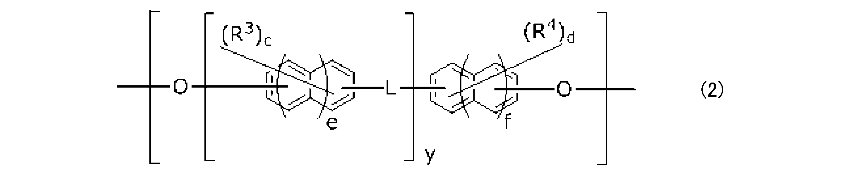
- the polymer preferably further has a repeating unit represented by the following general formula (2).
- R 3 and R 4 are each independently a halogen atom, a nitro group, a cyano group or a monovalent organic group having 1 to 20 carbon atoms, and c and d are each independently 0 to 8
- Each of e, f, and y is independently an integer of 0 to 2
- L is a single bond, -O-, -S-, -CO-, -SO-, -SO 2 -or a carbon number of 1 to 20 divalent organic groups.
- the halogen atom represented by R 3 and R 4 a fluorine atom, a chlorine atom, a bromine atom, and an iodine atom.
- Examples of the monovalent hydrocarbon group having 1 to 20 carbon atoms represented by R 3 and R 4 include a monovalent chain hydrocarbon group, a monovalent alicyclic hydrocarbon group, and a monovalent aromatic group. A hydrocarbon group etc. are mentioned.
- Examples of the monovalent chain hydrocarbon group include a methyl group, an ethyl group, an n-propyl group, an i-propyl group, an n-butyl group, an i-butyl group, an sec-butyl group and a t-butyl group, Alkyl groups such as n-pentyl group; alkenyl groups such as ethenyl group, propenyl group, butenyl group and pentenyl group; and alkynyl groups such as ethynyl group, propynyl group, butynyl group and pentynyl group.
- Examples of the monovalent alicyclic hydrocarbon group include monocyclic cycloalkyl groups such as cyclopropyl group, cyclobutyl group, cyclopentyl group and cyclohexyl group; and polycyclic cycloalkyl groups such as norbornyl group and adamantyl group; Examples thereof include monocyclic cycloalkenyl groups such as cyclopropenyl group, cyclobutenyl group, cyclopentenyl group and cyclohexenyl group; and polycyclic cycloalkenyl groups such as norbornenyl group.
- Examples of the monovalent aromatic hydrocarbon group include aryl groups such as phenyl group, tolyl group, xylyl group, naphthyl group and anthryl group; and aralkyl groups such as benzyl group, phenethyl group, phenylpropyl group and naphthylmethyl group. Etc.
- Examples of the monovalent halogenated hydrocarbon group having 1 to 20 carbon atoms represented by R 3 and R 4 include, for example, monovalents having 1 to 20 carbon atoms exemplified as the groups represented by R 3 and R 4 above.
- the group etc. which substituted some or all of the hydrogen atoms of the hydrocarbon group of these with the halogen atoms, such as a fluorine atom, a chlorine atom, a bromine atom, an iodine atom, etc. are mentioned.
- C1-C20 bivalent organic group represented by L a C1-C20 bivalent chain hydrocarbon group, a C1-C20 bivalent fluorinated chain carbonization is mentioned, for example examples thereof include a hydrogen group, a divalent aromatic hydrocarbon group having 6 to 20 carbon atoms, and a divalent fluorinated aromatic hydrocarbon group having 6 to 20 carbon atoms.
- Examples of the divalent chain hydrocarbon group include a methylene group, an ethylene group, an n-propylene group, an isopropylene group, an n-butylene group, a sec-butylene group, a t-butylene group, a neopentylene group, and 4-methyl. And -pentane-2,2-diyl group, nonane-1,9-diyl group and the like.
- Examples of the divalent alicyclic hydrocarbon group include monocyclic cycloalkyl groups such as cyclopropyl group, cyclobutyl group, cyclopentyl group and cyclohexyl group; and polycyclic cycloalkyl groups such as norbornyl group and adamantyl group; Examples thereof include monocyclic cycloalkenyl groups such as cyclopropenyl group, cyclobutenyl group, cyclopentenyl group and cyclohexenyl group; and polycyclic cycloalkenyl groups such as norbornenyl group.
- divalent aromatic hydrocarbon group examples include aryl groups such as phenyl group, tolyl group, xylyl group, naphthyl group and anthryl group; and aralkyl groups such as benzyl group, phenethyl group, phenylpropyl group and naphthylmethyl group.
- aryl groups such as phenyl group, tolyl group, xylyl group, naphthyl group and anthryl group
- aralkyl groups such as benzyl group, phenethyl group, phenylpropyl group and naphthylmethyl group.
- polymers described in, for example, JP-A-2015-209511, International Publication WO2016 / 143447, JP-A-2017-197725, JP-A-2018-024827, etc. can be exemplified.
- the content rate of the polymer in the composition for resin layers is 10 mass parts or more and 90 mass parts or less with respect to a total of 100 mass parts of the curable compound mentioned later and a polymer.
- the curable compound is a compound which is cured by irradiation of heat or light (for example, visible light, ultraviolet light, near infrared light, far infrared light, electron beam or the like), and may require a curing aid described later .
- heat or light for example, visible light, ultraviolet light, near infrared light, far infrared light, electron beam or the like
- an epoxy compound, a cyanate ester compound, a vinyl compound, a silicone compound, an oxazine compound, a maleimide compound, an allyl compound, an acrylic compound, a methacrylic compound, a urethane compound is mentioned, for example. These may be used alone or in combination of two or more.
- At least one of epoxy compounds, cyanate ester compounds, vinyl compounds, silicone compounds, oxazine compounds, maleimide compounds, and allyl compounds from the viewpoint of characteristics such as compatibility with the polymer, heat resistance, etc. It is preferable that it is at least 1 sort (s) among an epoxy compound, a cyanate ester compound, a vinyl compound, an allyl compound, and a silicone compound.
- the content of the curable compound in the composition for resin layer is preferably 10 parts by mass or more and 90 parts by mass or less, and 20 parts by mass or more and 80 parts by mass or less with respect to 100 parts by mass of the composition for resin layer It is more preferable that
- polymerization initiators such as a photoinitiator (a photo radical generator, a photo-acid generator, a photo base generator), can be mentioned, for example.
- a photoinitiator a photo radical generator, a photo-acid generator, a photo base generator
- onium salt compounds, sulfone compounds, sulfonic acid ester compounds, sulfoneimide compounds, disulfonyldiazomethane compounds, disulfonylmethane compounds, oxime sulfonate compounds, hydrazine sulfonate compounds, triazine compounds, triazine compounds, nitrobenzyl compounds Examples thereof include benzylimidazole compounds, organic halides, metal salts of octylate, and disulfone. Any of these curing assistants may be used alone or in combination of two or more.
- the content of the curing assistant in the composition for resin layer is preferably 5 parts by mass or more and 20 parts by mass or less, and is 5 parts by mass or more and 10 parts by mass or less with respect to 100 parts by mass of the composition for resin layer It is more preferable that
- the composition for resin layer may contain a solvent as needed.
- a solvent for example, amides such as N, N-dimethylacetamide, N, N-dimethylformamide, N-methyl-2-pyrrolidone, N-ethyl-2-pyrrolidone, 1,3-dimethyl-2-imidazolidinone and the like Solvent; ester solvents such as ⁇ -butyrolactone and butyl acetate; ketone solvents such as cyclopentanone, cyclohexanone, methyl ethyl ketone and benzophenone, ether solvents such as 1,2-methoxyethane and diphenyl ether, 1-methoxy-2- Multifunctional solvents such as propanol and propylene glycol methyl ether acetate; sulfone solvents such as sulfolane, dimethylsulfoxide, diethylsulfoxide, diethylsulfoxide, dimethylsulf
- composition for resin layers contains a solvent
- 2000 mass parts or less are preferable with respect to 100 mass parts of compositions for resin layers except a solvent, and 200 mass parts or less are more preferable.
- the composition for resin layer may contain other components as needed.
- other components include antioxidants, reinforcing agents, lubricants, flame retardants, antibacterial agents, colorants, mold release agents, foaming agents, and polymers other than the above-mentioned polymers.
- composition for resin layers ⁇ Method of Preparing Composition for Resin Layer>
- a polymer, a curable compound, and other additives as needed for example, other components, such as a hardening adjuvant, a solvent, antioxidant, etc.
- the form of the composition can be liquid, paste or the like.
- the laminate for a high frequency circuit according to the present embodiment includes a metal layer. It is preferable to use a metal foil or a sputtered film as the metal layer. Copper foil is preferred as the metal foil. There are electrolytic foil and rolling foil as a kind of copper foil, but either may be used.
- the surface roughness Ra of the metal layer is preferably 10 to 300 nm, more preferably 30 to 200 nm, and particularly preferably 30 to 100 nm.
- the adhesion between the resin layer and the metal layer can be further improved when forming a laminate for a high frequency circuit.
- the thickness in the plane of the laminate for high frequency circuits can be made more uniform, and peeling of the resin layer and the metal layer can be suppressed when winding the laminate for high frequency circuits into a roll shape. it can.
- the surface roughness Ra of the metal layer refers to the "arithmetic average roughness" measured in accordance with JIS B 0601-2001.
- the thickness of the metal layer is preferably 3 to 50 ⁇ m, more preferably 5 to 40 ⁇ m, and particularly preferably 7 to 35 ⁇ m.
- a thin metal foil may be used as it is as long as the surface roughness Ra falls within the above range, but the surface is physically or chemically treated to obtain a surface roughness Ra. May be used in the above range.
- Methods of controlling the surface roughness of the metal foil include methods such as etching treatment (acid treatment etc.), laser treatment, electrolytic plating, electroless plating, sputtering treatment, sand blasting etc. to the metal foil, but it is limited to these It is not a thing.
- the method of manufacturing the laminate for a high frequency circuit according to this embodiment is not particularly limited as long as the resin layer and the metal layer can be laminated in contact with each other. “The resin layer and the metal layer are in contact” is not limited to the case where one surface of the resin layer is in contact with the entire surface of the metal layer, and at least a part of one surface of the resin layer is in contact with the metal layer Including the case.
- FIGS. 1A to 1D are diagrams schematically showing cross sections in respective steps of Production Example A.
- FIG. Production Example A will be described with reference to FIGS. 1A to 1D.
- Step A1 As shown to FIG. 1A, the composition for resin layers is coated on peeling layer 10, B-stage resin layer 12 is formed, and "B-stage resin layer / peeling layer laminated body" (it also calls “B-stage sheet”. Make.).
- peeling layer 10 known films such as a PET film can be used. Although it does not specifically limit as a PET film, For example, Panac Protect MK38S etc. made by PANAC KK can be used.
- the coating method of the composition for resin layers can use a well-known coating method, for example, it is preferable to adjust and coat a film thickness using a bar coater.
- the B-stage resin layer 12 of a semi-hardened state using well-known heating means, such as oven.
- the heating temperature is preferably 50 to 150 ° C., and more preferably 70 to 130 ° C.
- it may be heated in two stages, for example, 50 to 100 ° C. and 100 to 150 ° C.
- less than 30 minutes are preferable and, as for the sum total of heating time, less than 20 minutes are more preferable.
- the surface roughness Ra of the B-stage resin layer 12 exposed to the surface is preferably 1 to 100 nm, and more preferably 10 to 50 nm.
- the surface roughness Ra of the B-stage resin layer in the present invention means “arithmetic average roughness” measured in accordance with JIS B 0601-2001.
- the elastic modulus (MPa) of the B-stage resin layer 12 is preferably 1 MPa or more, more preferably 3 MPa or more, at 50 ° C. or more and less than 80 ° C. under measurement conditions of 1 Hz. Further, the minimum value of the elastic modulus (MPa) in the temperature range of 80 ° C. or more and 200 ° C. or less is preferably 20 MPa or less, and more preferably 15 MPa or less.
- the elastic modulus of the B-stage resin layer is in each temperature range, when the laminate for a high frequency circuit is manufactured by heat pressing, the unevenness of the wiring portion and the non-wiring portion can be suppressed, and the transmission loss is suppressed. be able to.
- Step A2 As shown in FIG. 1B, the exposed resin layer surface 13 of the “B-stage resin layer / peeling layer laminate” prepared in step A1 is bonded to the metal layer 14 to form “metal layer / B-stage resin layer / peeling layer lamination”. Create the body.
- the surface roughness Ra of the metal layer 14 to be bonded to the resin layer surface 13 is preferably 10 to 300 nm, more preferably 30 to 200 nm, and particularly preferably 30 to 100 nm.
- thermocompression bonding At the time of bonding, after the resin layer surface 13 of the “B-stage resin layer / peeling layer laminate” and the metal layer 14 are superimposed, further heated rolls (also referred to as “heat rolls” in the present specification). It is preferable to carry out thermocompression bonding using a metal etc.
- the line load at the time of thermocompression bonding is preferably 1 to 19 kN / m, and more preferably 5 to 18 kN / m.
- the temperature for thermocompression bonding is preferably 50 to 200 ° C., more preferably 50 to 150 ° C., and particularly preferably 70 to 130 ° C.
- annealing treatment is performed by subsequently bringing the “metal layer / B-stage resin layer / peeling layer laminate” immediately after bonding into contact with a heated roll or passing through a heating furnace. May be Such annealing treatment may be performed at a temperature equal to or higher than the melting point of the resin, but is preferably 100 to 250 ° C., and more preferably 110 to 230 ° C.
- the heating time is not particularly limited, but preferably 5 to 600 seconds, more preferably 10 to 300 seconds.
- the peeling layer can be peeled well in the manufacturing process.
- the "metal layer / B stage resin layer / exfoliation layer layered product immediately after bonding" mentioned above is processed continuously, and the layered product which carried out pasting in a manufacturing line which pastes a layered product It is the process of processing in-line succeedingly after bonding process, without taking out from a manufacturing line.
- Step A3 As shown to FIG. 1C, the peeling layer 10 is peeled from the "metal layer / B stage resin layer / peeling layer laminated body" produced at process A2, and the resin layer surface 11 and metal foil 16 which were exposed as needed are stuck. Match.
- the peeling layer 10 is peeled off from the “metal layer / B-stage resin layer / peeling layer laminate” and the exposed B-stage resin layer surface 11 and the metal layer 16 are bonded together, the exposed resin layer surface 11 and the metal layer 16 It is preferable to heat-pressure-bond using the heat roll etc. further. The same conditions as the process A2 are preferable for the thermocompression bonding.
- surface roughness Ra of the resin layer surface 11 which peeled and exposed the peeling layer 10 from "a metal layer / B stage resin layer / peeling layer laminated body" is 1 to 100 nm, and is 10 to 50 nm. Is more preferred.
- the adhesiveness of a resin layer, a metal layer, and resin layers can be improved more.
- Step A4 As shown in FIG. 1D, the B-stage resin layer 12 is cured to form the C-stage resin layer 18, whereby a laminate 100 for a high frequency circuit is obtained.
- the laminate obtained in step A3 is preferably heated to 50 to 200 ° C. using a known heating means such as an oven, and may be heated to 100 to 200 ° C. More preferable. When heating, it may be heated in two stages, for example, 50 to 100 ° C. and 100 to 200 ° C. Moreover, less than 5 hours are preferable, and less than 3 hours are more preferable. By heating under the conditions of temperature and time within the above range, a C-stage resin layer with high film thickness uniformity can be produced, in which the B-stage resin layer is cured.
- FIGS. 2A to 2C schematically show cross sections in respective steps of Production Example B.
- FIGS. Production Example B will be described with reference to FIGS. 2A to 2C.
- Step B1 As shown to FIG. 2A, the composition for resin layers is coated to the metal layer 20, the B-stage resin layer 22 is formed, and "a metal layer / B-stage resin layer laminated body" is produced.
- the coating method of the composition for resin layers can use a well-known coating method, for example, it is preferable to adjust and coat a film thickness using a bar coater.
- the B-stage resin layer 22 of a semi-hardened state using well-known heating means, such as oven.
- the heating temperature is preferably 50 to 150 ° C., and more preferably 70 to 130 ° C.
- it may be heated in two stages, for example, 50 to 100 ° C. and 100 to 150 ° C.
- less than 30 minutes are preferable and, as for the sum total of heating time, less than 20 minutes are more preferable.
- Step B2 As shown to FIG. 2B, the metal layer 24 is bonded together to the exposed resin layer surface 23 of the "metal layer / B stage resin layer laminated body" produced at process B1, and "metal layer / B stage resin layer / metal layer lamination
- the metal layer 24 is bonded to the exposed resin layer surface 23, it is preferable that the exposed resin layer surface 23 and the metal layer 24 be stacked, and then heat compression be performed using a heat roll or the like.
- the conditions similar to the said process A2 are preferable for thermocompression bonding.
- step B2 even if “metal layer / B-stage resin layer / metal layer” immediately after bonding is subsequently brought into contact with a heated roll or passed through a heating furnace, annealing treatment is performed. Good. The annealing treatment is preferably performed under the same conditions as in the step A2.
- the surface roughness Ra of the exposed resin layer surface 23 is preferably 1 to 100 nm, and more preferably 10 to 50 nm.
- the surface roughness Ra of the metal layer 24 to be bonded to the resin layer surface 23 is preferably 10 to 300 nm, more preferably 30 to 200 nm, and particularly preferably 30 to 100 nm.
- Step B3 As shown in FIG. 3C, by curing the B-stage resin layer 22 to form the C-stage resin layer 26, a laminate 200 for a high frequency circuit can be obtained.
- the “metal layer / B stage resin layer / metal layer laminate” prepared in step B2 is preferably heated to 50 to 200 ° C. using a known heating means such as an oven, and is preferably heated to 100 to 200 ° C. It is more preferable to do. When heating, it may be heated in two stages, for example, 50 to 100 ° C. and 100 to 200 ° C. Moreover, less than 5 hours are preferable, and less than 3 hours are more preferable. By heating under the conditions of temperature and time within the above range, a C-stage resin layer 26 with high film thickness uniformity can be produced, in which the B-stage resin layer 22 is cured.
- the laminated wound body according to the present embodiment has a structure in which a metal layer and a resin layer having a dielectric loss tangent of 0.001 to 0.01 at a frequency of 10 GHz at 23 ° C. are in contact with each other.
- the laminate for high frequency circuits is characterized in that it is wound around a core having a radius of 10 to 100 mm.
- FIG. 3 is a perspective view which shows an example of the laminated body winding body which concerns on this embodiment.
- FIG. 4 is a perspective view showing an example of a core that can be used in the present embodiment.
- a laminate wound body 300 according to the present embodiment includes a core 30 and a laminate 40 for a high frequency circuit wound around the core 30.
- Such a laminate for a high frequency circuit is used or stored in the form of a laminate wound body obtained by forming a long sheet having a certain width for efficient processing and winding it around a core. Is common.
- the laminated body wound body according to the present embodiment preferably uses a substantially cylindrical core.
- a substantially cylindrical core by reducing the radius of the cylindrical core and reducing the radius of curvature as much as possible, miniaturization can be achieved even with a roll in which a laminate for a high frequency circuit of the same length is wound, and productivity can be increased. It can be improved.
- a laminate wound body having a small radius of curvature there is a tendency that winding defects easily remain in the laminate for high frequency circuits, and the processing of the laminate for high frequency circuits becomes difficult. For this reason, in order to suppress the winding wrinkles which remain in the layered product for high frequency circuits, it was difficult to make the curvature radius of a layered product winding object small.
- an adhesive layer is interposed to improve the adhesion between the resin layer and the metal layer. For this reason, when storing the laminated body wound body which wound the conventional laminated body for high frequency circuits on the core, since the adhesive layer is deteriorated and hardened due to an external factor, it is wounded when it is pulled out. Was easy to occur.
- a high frequency circuit including a structure in which a metal layer and a resin layer having a dielectric dissipation factor of 0.001 to 0.01 at a frequency of 10 GHz at 23 ° C. are in contact with each other.
- the winding core 30 and the high frequency circuit laminate 40 may or may not be joined using a joining member.
- the winding core 30 when the winding core 30 has the step portion 32, the winding core 30 is joined to the step portion 32 of the winding core 30 via the bonding member at the end of the high frequency circuit laminate 40. It can be rotated to wind up the laminate for high frequency circuits 40, and the laminate winding body 300 can be manufactured.
- the winding core etc. which are described, for example in utility model registration 3147706 can be used.
- the kind of joining member is not specifically limited, Various joining members can be used, For example, an adhesive agent, an adhesive, and a double-sided tape etc. can be used. These may use only 1 type and may use 2 or more types together. Further, the bonding member may bond the entire length in the width direction of the high-frequency circuit laminate 40 to the core 30 or may connect only a part of the bonding member.
- the radius of the winding core 30 is 10 to 100 mm, preferably 10 to 50 mm, and more preferably 15 to 40 mm.
- the radius of the winding core 30 is in the above range, when the laminate for high frequency circuit 40 is drawn out from the laminate winding body 300 and processed, a joint portion between the laminate for high frequency circuit 40 and the winding core 30 (wound It is possible to effectively suppress the formation of the pressing mark 41 as shown in FIG. 5 resulting from the step in the start portion).
- a push mark 41 is a main factor of the fall of a yield in the laminated body process for high frequency circuits, it is one of the winding rolls which should be suppressed as much as possible for productivity improvement.
- the height of the step portion 32 is preferably 50 to 200 ⁇ m, more preferably 60 to 180 ⁇ m, and particularly preferably 70 to 150 ⁇ m.
- the height of the step portion 32 is particularly preferably the thickness ( ⁇ m) ⁇ 10 ⁇ m of the laminate 20 for a high frequency circuit.
- the winding core 30 Although it does not specifically limit as a material of the winding core 30, Paper, a metal, a thermoplastic resin, etc. can be mentioned. When the material of the winding core 30 is paper, the surface may be coated with resin or the like. Examples of the metal include SUS, iron, aluminum and the like.
- thermoplastic resin olefin resin (polyethylene, polypropylene etc.), styrene resin (ABS resin, AES resin, AS resin, AS resin, MBS resin, polystyrene etc.), polyvinyl chloride, vinylidene chloride resin, methacrylic resin, polyvinyl alcohol Styrene-based block copolymer resin, polyamide, polyacetal, polycarbonate, modified polyphenylene ether, polyester (polybutylene terephthalate, polyethylene terephthalate etc.), fluorocarbon resin, polyphenylene sulfide, polysulfone, amorphous polyarylate, polyetherimide, polyether sulfone, poly Ether ketones, liquid crystal polymers, polyamide imides, thermoplastic polyimides, syndio-type polystyrene and the like can be mentioned. These may use only 1 type and may use 2 or more types together.
- the material of the winding core 30 is a thermoplastic resin,
- the method of winding up the laminated body for high frequency circuits bonded in a roll shape is not particularly limited, and may be according to the method used in the manufacture of a laminate or film for high frequency circuits.
- Circuit board flexible printed circuit board
- a circuit board such as an FPC can be manufactured using the laminate for a high frequency circuit of the present invention described above. Such a circuit board can reduce transmission loss even when driven at high frequency by using the laminate for a high frequency circuit of the present invention as at least a part of the laminated structure.
- Such a circuit board may be manufactured by a known method, as long as it has the laminate for a high frequency circuit of the present invention as a part of a laminated structure, and, for example, WO 2012/014339, JP 2009
- the production process can be applied by applying the production process described in JP-231770 A and the like.
- a circuit board is manufactured by laminating the laminate for high frequency circuits of the present invention, patterning the metal layer of the laminate for high frequency circuits of the present invention by etching, drilling holes, cutting to a required size, etc. can do.
- Such circuit boards are, for example, Step (a): a step of laminating a resin film on a circuit substrate to form a resin layer, Step (b): Step of flattening the resin layer by heating and pressing, Step (c): a step of further forming a circuit layer on the resin layer, Etc. can be manufactured.
- the method of laminating the resin film on the circuit substrate in the step (a) is not particularly limited, and examples thereof include a method of laminating using a multistage press, a vacuum press, an atmospheric pressure laminator, and a laminator heated and pressurized under vacuum.
- the method of using a laminator which heats and presses under vacuum is preferable. Thereby, even if the circuit substrate has a fine wiring circuit on the surface, there is no void, and it is possible to bury the circuit with the resin.
- the laminating conditions are not particularly limited, but it is preferable that the pressure bonding temperature is 70 to 130 ° C. and the pressure bonding pressure is 1 to 11 kgf / cm 2 , and the layers are laminated under reduced pressure or vacuum.
- the laminate may be batch or may be continuous on a roll.
- the circuit substrate is not particularly limited, and a glass epoxy substrate, a metal substrate, a polyester substrate, a polyimide substrate, a BT resin substrate, a thermosetting polyphenylene ether substrate, a fluorine resin substrate and the like can be used.
- the circuit surface of the surface on which the resin film of the circuit board is laminated may be roughened in advance.
- the number of circuit layers of the circuit board is not limited. For example, in the case of producing a printed wiring board for millimeter wave radar, it is possible to freely select 2 to 20 layers according to the design.
- the resin film and the circuit substrate laminated in the step (a) are heated and pressurized to be planarized.
- the conditions are not particularly limited, but a temperature of 100 ° C. to 250 ° C., a pressure of 0.2 to 10 MPa, and a time range of 30 to 120 minutes are preferable, and 150 ° C. to 220 ° C. are more preferable.
- a circuit layer is further formed on the resin layer produced by heating and pressing the resin film and the circuit substrate.
- the method for forming the circuit layer formed on the resin layer is not particularly limited.
- the circuit layer may be formed by an etching method such as a subtractive method, a semi-additive method, or the like.
- an etching resist layer having a shape corresponding to a desired pattern shape is formed on a metal layer, and the metal layer on the removed portion of the resist is dissolved and removed with a chemical solution by subsequent development processing. To form a desired circuit.
- a metal film is formed on the surface of a resin layer by electroless plating, a plating resist layer having a shape corresponding to a desired pattern is formed on the metal film, and then a metal layer is formed by electrolytic plating. Then, an unnecessary electroless plating layer is removed by a chemical solution or the like to form a desired circuit layer.
- holes such as via holes may be formed in the resin layer as required.
- the formation method of a hole is not limited, NC drill, a carbon dioxide gas laser, UV laser, YAG laser, plasma etc. are applicable.
- the glass transition temperature (Tg) is measured at a frequency of 1 Hz and a heating rate of 10 ° C./min using a dynamic viscoelasticity measuring apparatus (manufactured by Seiko Instruments Inc., “DMS 7100”), and the loss tangent is considered to be a maximum. Temperature. The loss tangent was the storage modulus divided by the loss modulus.
- the weight average molecular weight (Mw) was measured using a GPC apparatus (“HLC-8320 type” manufactured by Tosoh Corporation) under the following conditions.
- Sample concentration 0.75% by mass
- Sample injection volume 50 ⁇ L
- Detector Differential Refractometer Standard substance: Monodispersed polystyrene
- Example 1 4.2.1. Preparation of B-stage resin layer / release layer laminate 50 parts of polymer P-1, 50 parts of 2,2'-bis (4-cyanatophenyl) propane (made by Tokyo Chemical Industry Co., Ltd.) as a curable compound, cured A resin layer composition was prepared by mixing 5 parts of 1-benzyl-2-methylimidazole (manufactured by Mitsubishi Chemical Corporation, product name “BMI 12”) and 160 parts of cyclopentanone as an auxiliary.
- BMI 12 1-benzyl-2-methylimidazole
- the composition for resin layer prepared above on a PET film with a thickness of 100 ⁇ m (Teijin Film Solutions Ltd., Teijin Tetron Film G2) as a release layer so that the film thickness after curing is 25 ⁇ m Coated and heated at 70 ° C. for 10 minutes using an oven, and further heated at 130 ° C. for 10 minutes to laminate a B-stage resin layer on a PET film “B-stage resin layer / peeling layer laminate I got
- ⁇ Surface roughness Ra> The surface of the resin layer of the “B-stage resin layer / peeling layer laminate” obtained above was measured using a white interference microscopic device (New View 5032 manufactured by ZYGO), and 10 ⁇ m in accordance with JIS B0601-2001. The “arithmetic mean roughness” calculated for the range of 10 ⁇ m was taken as the surface roughness Ra. The results are shown in Table 1.
- the surface roughness Ra of the copper foil was measured using a white interference microscope (New View 5032 manufactured by ZYGO), and the “arithmetic average roughness calculated for a range of 10 ⁇ m ⁇ 10 ⁇ m according to JIS B0601-2001. Surface roughness Ra. The results are shown in Table 1.
- the release layer (PET film) was peeled off from the “metal layer / B stage resin layer / release layer laminate” obtained above, and the exposed resin layer surface and a copper foil with a thickness of 18 ⁇ m. (Mitsui Metals Co., Ltd., Model No.
- TQ-M4-VSP surface roughness 110 nm
- a heat roll of 150 ° C under a line load of 10 kN / m then using an oven Copper foil (film thickness 18 ⁇ m) / C stage resin layer (film thickness 25 ⁇ m) / Copper foil (film thickness 18 ⁇ m) with copper foil laminated on both sides of the C stage resin layer by heating at 250 ° C.
- Tg Glass transition temperature
- the copper foil was removed by etching the produced laminate for a high frequency circuit, and a resin film for evaluation was produced.
- a test piece (width 3 mm ⁇ length 1 cm) was cut out of the produced resin film, and the glass transition temperature (Tg) was measured with a DMS tester (manufactured by Seiko Instruments Inc., model number “EXSTAR 4000”). The results are shown in Table 1.
- the laminate for a high frequency circuit prepared above is pasted on a thick paper core of width 250 mm and core radius 40 mm and a double-sided tape 10 ⁇ m thick across the length 100 mm at the center in the width direction I put it. Thereafter, the produced high-frequency circuit laminate was bonded to a double-sided tape, and then the high-frequency circuit laminate was wound around 1,000 layers around a winding core with a winding tension of 150 N / m to produce a laminate-wound body.
- a copper foil is patterned using a photosensitive dry film on one side of the laminate for a high frequency circuit prepared above, and the line width is 40, 45, 50, 55, 60 ⁇ m, each at a pitch of 150 ⁇ m.
- a copper wiring pattern having a pitch of 750 ⁇ m and a line width of 200, 220, 240, 260, 280 ⁇ m, respectively.
- ⁇ Transmission loss evaluation> The transmission loss at a frequency of 20 GHz at 25 ° C. was measured for the circuit board manufactured above using a measurement probe (Cascade Microtech Co., Ltd., single (ACP40GSG250) and a vector network analyzer (Keysight technology E8363B). In the case of 5 dB / 100 mm or more, it was judged to be good.
- Both sides of the laminate for a high frequency circuit prepared above are etched on both sides so that the thickness of the copper foil is 9 ⁇ m, and the copper foil is patterned using a photosensitive dry film, and the line width is 50 ⁇ m with a pitch of 100 ⁇ m.
- the copper wiring pattern of Next from the “metal layer / B-stage resin layer / peeling layer laminate” produced above, the peeling layer (PET film) is peeled, and the resin layer exposed and peeled is in contact with the produced copper wiring pattern The sample was placed on both sides, further sandwiched by a mirror plate, heated and pressurized under press conditions of 120 ° C./1.1 MPa / 2 minutes, and further heated at 250 ° C.
- the copper foil was patterned using a photosensitive dry film, and a copper wiring pattern having a pitch of 100 ⁇ m and a line width of 50 ⁇ m was produced on both sides.
- the peeling layer (PET film) is peeled from the “B-stage resin layer / peeling layer laminate” produced above, and the resin layer on the peeling surface is disposed on both sides so that the produced copper wiring pattern is in contact. Furthermore, after sandwiching with a mirror plate and heating / pressure forming under press conditions of 120 ° C./1.1 MPa / 2 minutes, heating was further carried out at 250 ° C. for 3 hours to prepare an evaluation substrate having four layers of copper wiring.
- the cross-sectional shape of the produced evaluation substrate is observed using a scanning electron microscope, and it is judged that it is practicable and good if the difference between the concave and the convex is 5% or less, and it is impracticable if it exceeds 5%. I judged it to be bad.
- the results are shown in Table 1.
- Example 2 Comparative Examples 1 to 3, Reference Example 1
- Example 2 The same as Example 1, except that the composition for the resin layer was changed to the composition of Table 1, and the type of metal film, various film thicknesses, lamination conditions, and preparation conditions of laminate wound body were changed as shown in Table 1.
- a laminate for a high frequency circuit was produced and evaluated by the method. The results are shown in Table 1.
- Example 8 For the resin layer prepared in Example 1 so that the film thickness after curing becomes 25 ⁇ m on a 18 ⁇ m thick copper foil (Mitsui Metals, model number “TQ-M4-VSP”, surface roughness 110 nm) The composition is applied using a bar coater, heated at 70 ° C. for 10 minutes using an oven, and further heated at 130 ° C. for 10 minutes to obtain a “metal layer having a laminated structure of copper foil / B stage resin layer / B-stage resin layer laminate "was produced.
- Comparative example 4 The composition for resin layer was produced similarly to Example 1 so that it might become a composition of Table 1, and 18 ⁇ m thick copper foil (made by Mitsui Metals, model number "TQ-M4-VSP", surface roughness 110 nm) The composition for a resin layer is coated using a bar coater so that the film thickness after curing becomes 25 ⁇ m, heated at 70 ° C. for 10 minutes using an oven, and then heated at 130 ° C. for 10 minutes, Furthermore, it heated at 250 degreeC for 3 hours.
- Table 1 shows the compositions of the resin layer compositions used in the examples and the comparative examples, and the evaluation results of the layers, the laminate for high frequency circuits, and the laminate wound body.
- the laminate wound body obtained in Examples 1 to 8 is wound by winding the laminate for a high frequency circuit in which the transmission loss of the electric signal in the high frequency circuit is reduced, and stored. It was found that even in the case where it was done, curling can be effectively suppressed.
Landscapes
- Engineering & Computer Science (AREA)
- Microelectronics & Electronic Packaging (AREA)
- Laminated Bodies (AREA)
Abstract
高周波回路における電気信号の伝送損失を低減し、平滑性に優れた回路基板を製造可能な高周波回路用積層体を提供する。 本発明に係る高周波回路用積層体は、金属層と、樹脂層とが接して積層され、前記樹脂層の弾性率が0.1~3GPaであり、23℃において前記樹脂層の周波数10GHzにおける誘電正接が0.001~0.01であり、かつ、比誘電率が2~3であることを特徴とする。
Description
本発明は、樹脂層と金属層とを貼り合わせてなる高周波回路用積層体及びその製造方法、並びにBステージシートに関する。また、本発明は、高周波回路基板として好適に使用される積層体捲回体に関する。
近年の情報端末機器の高性能化やネットワーク技術の飛躍的進歩に伴い、情報通信分野で扱う電気信号は高速・大容量伝送に向けた高周波数化が進んでいる。これに対応するため、使用されるプリント配線板にも高周波信号や高速デジタル信号を伝送・処理する上で課題となる伝送損失を低減できる低誘電率(低εr)・低誘電正接(低tanδ)材料に対する要求が高まっている(例えば、特許文献1~4参照)。
プリント配線板としては、フレキシブルプリント基板(以下、「FPC」ともいう)やフレキシブルフラットケーブル(以下、「FFC」ともいう)が、電子・電気機器に使用されている。FPCは、絶縁体層と銅箔層とからなる銅張積層体(CCL)を加工して電気回路を形成した後、該回路部を保護するために絶縁層と接着剤層からなるカバーレイ(CL)の接着剤部を回路部へ取り付ける工程を経て製造される。また、FFCは、絶縁体層と接着剤層からなる基材と配線状に形成した銅箔等の導体を用い、基材の接着剤部同士の間に導体を複数本並べ、接着して得られる電気回路である。
しかしながら、電気信号は高周波になればなるほど減衰しやすく、伝送損失が大きくなる傾向にある。そのため、次世代高周波(10GHz以上)対応実装基板では、配線間クロストーク低減のための低誘電や電気信号の伝送損失を抑制するための低誘電損失特性が、絶縁体材料に必要不可欠な特性となっている。また、電気信号の伝送損失を抑制するためには、実装基板が平滑性に優れていることも重要である。特にFPCやFFCでは、樹脂層と金属層とを積層させるために接着剤が使用されるが、接着剤によって形成される接着層が実装基板の低誘電損失特性や平滑性を損なう一因であると考えられる。
さらに、接着剤を介在させた樹脂層と金属層との積層体は、巻芯に捲回させた捲回体として保管した場合に、外的な要因(例えば保管環境)により接着層が変質して硬化するために、引き出したときに巻癖が発生しやすいという課題があった。
本発明は上記実情に鑑みてなされたものであり、高周波回路における電気信号の伝送損失を低減し、平滑性に優れた回路基板を製造可能な高周波回路用積層体を提供することを課題とする。また、本発明は、低温での貼り合わせによる製造が可能であり、樹脂層と金属層間の接着性に優れる高周波回路用積層体の製造方法を提供することを課題とする。
さらに、高周波信号の伝送損失を低減することが可能な高周波回路用積層体を巻芯に捲回して保管した場合であっても巻癖を効果的に抑制できる積層体捲回体を提供することを課題とする。
本発明は上述の課題の少なくとも一部を解決するためになされたものであり、以下の態様または適用例として実現することができる。
[適用例1]
本発明に係る高周波回路用積層体の一態様は、
金属層と、樹脂層とが接して積層され、
前記樹脂層の弾性率が0.1~3GPaであり、
23℃において前記樹脂層の周波数10GHzにおける誘電正接が0.001~0.01であり、かつ、比誘電率が2~3であることを特徴とする。
本発明に係る高周波回路用積層体の一態様は、
金属層と、樹脂層とが接して積層され、
前記樹脂層の弾性率が0.1~3GPaであり、
23℃において前記樹脂層の周波数10GHzにおける誘電正接が0.001~0.01であり、かつ、比誘電率が2~3であることを特徴とする。
[適用例2]
適用例1の高周波回路用積層体において、
前記樹脂層と前記金属層との剥離強度が5N/cm以上であることができる。
適用例1の高周波回路用積層体において、
前記樹脂層と前記金属層との剥離強度が5N/cm以上であることができる。
[適用例3]
適用例1または適用例2の高周波回路用積層体において、
前記樹脂層の厚さが10~100μmであり、かつ、前記金属層の厚さが10~50μmであることができる。
適用例1または適用例2の高周波回路用積層体において、
前記樹脂層の厚さが10~100μmであり、かつ、前記金属層の厚さが10~50μmであることができる。
[適用例4]
適用例1ないし適用例3のいずれか一例の高周波回路用積層体において、
厚さが50~200μmであることができる。
適用例1ないし適用例3のいずれか一例の高周波回路用積層体において、
厚さが50~200μmであることができる。
[適用例5]
本発明に係るフレキシブルプリント基板の一態様は、
適用例1ないし適用例4のいずれか一例の高周波回路用積層体を備えることを特徴とする。
本発明に係るフレキシブルプリント基板の一態様は、
適用例1ないし適用例4のいずれか一例の高周波回路用積層体を備えることを特徴とする。
[適用例6]
本発明に係る積層体捲回体の一態様は、
適用例1ないし適用例4のいずれか一例の高周波回路用積層体が、半径10~100mmの巻芯に捲回されてなるものである。
本発明に係る積層体捲回体の一態様は、
適用例1ないし適用例4のいずれか一例の高周波回路用積層体が、半径10~100mmの巻芯に捲回されてなるものである。
[適用例7]
本発明に係る高周波回路積層体の製造方法の一態様は、
表面粗さRaが1~100nmのBステージ樹脂層と、表面粗さRaが10~300nmの金属層とを、50~200℃に加熱して1~19kN/mの線荷重を掛けて貼り合わせる工程を含むことを特徴とする。
本発明に係る高周波回路積層体の製造方法の一態様は、
表面粗さRaが1~100nmのBステージ樹脂層と、表面粗さRaが10~300nmの金属層とを、50~200℃に加熱して1~19kN/mの線荷重を掛けて貼り合わせる工程を含むことを特徴とする。
[適用例8]
本発明に係るBステージシートの一態様は、
Bステージ樹脂層と、前記Bステージ樹脂層の少なくとも一方の面に形成された剥離層と、を有するBステージシートであって、
前記Bステージ樹脂層が硬化されてCステージ樹脂層となったときの、
前記Cステージ樹脂層の弾性率が0.1~3GPaであり、
前記Cステージ樹脂層の23℃での周波数10GHzにおける誘電正接が0.001~0.01であり、かつ、比誘電率が2~3であることを特徴とする。
本発明に係るBステージシートの一態様は、
Bステージ樹脂層と、前記Bステージ樹脂層の少なくとも一方の面に形成された剥離層と、を有するBステージシートであって、
前記Bステージ樹脂層が硬化されてCステージ樹脂層となったときの、
前記Cステージ樹脂層の弾性率が0.1~3GPaであり、
前記Cステージ樹脂層の23℃での周波数10GHzにおける誘電正接が0.001~0.01であり、かつ、比誘電率が2~3であることを特徴とする。
本発明に係る高周波回路用積層体によれば、高周波回路における電気信号の伝送損失を低減し、平滑性に優れた回路基板を製造することができる。また、本発明に係る高周波回路用積層体の製造方法によれば、低温での貼り合わせによる製造が可能であり、樹脂層と金属層間の接着性に優れる高周波回路用積層体を製造することができる。さらに、本発明に係る積層体捲回体によれば、高周波信号の伝送損失を低減することが可能な高周波回路用積層体を巻芯に捲回して保管した場合であっても巻癖を効果的に抑制できる。
以下、本発明に係る好適な実施形態について詳細に説明する。なお、本発明は、以下に記載された実施形態のみに限定されるものではなく、本発明の要旨を変更しない範囲において実施される各種の変形例も含むものとして理解されるべきである。
本明細書において、「~」を用いて記載された数値範囲は、「~」の前後に記載される数値を下限値及び上限値として含む意味である。
1.高周波回路用積層体
本明細書で用いられる用語を以下のように定義する。
・「高周波信号」とは、10GHz以上の周波数の電気信号または電波のことをいう。
・「高周波回路用積層体」とは、10GHz以上の周波数で駆動する高周波回路を製造する際に使用するための積層体のことをいう。
・「Bステージ樹脂層」とは、樹脂が半硬化した状態の層のことをいう。
・「Cステージ樹脂層」とは、樹脂が完全に硬化した状態の層のことをいう。なお、本願発明において、「Cステージ樹脂層」を単に「樹脂層」ということもある。
・「捲回体」とは、巻芯上に、一様の幅の高周波回路用積層体が所定の長さ分だけ捲回されたものをいう。巻長や幅は特に限定されるものではないが、通常巻長は0.5~100m、幅は数十~1000mm程度である。
本実施形態に係る高周波回路用積層体は、金属層と樹脂層とが接して積層されてなるものであり、金属層と樹脂層との間にプライマー樹脂層のような接着層を介在しない。一般的な回路用積層体は、導電機能を担う金属層と絶縁機能を担う樹脂層との密着性を向上させるために、樹脂層と金属層との間に接着層を介在させている。接着層は、主に極性官能基を有する重合体を含有する接着剤を用いて、塗布などの方法によって形成される。しかしながら、このような接着層は、電気特性が悪いので、絶縁機能を担う樹脂層の実効誘電率や実効誘電損失が大きくなってしまい、高周波回路には不適であった。これに対して、本実施形態に係る高周波回路用積層体は、接着剤を使用しなくても金属層と樹脂層との密着性が良好であり、金属層と樹脂層とが接して積層されることによって、樹脂層の実効電気特性を劣化させずに高周波回路に適した積層体を得ることに成功した。
本実施形態で用いられる高周波回路用積層体は、樹脂層と金属層との剥離強度が5N/cm以上であることが好ましく、5.3N/cm以上であることがより好ましく、6N/cm以上であることが特に好ましい。本実施形態で用いられる高周波回路用積層体は、上記範囲の剥離強度を有するため、接着剤を使用しなくても金属層と樹脂層との密着性が良好である。なお、剥離強度は、「IPC-TM-650 2.4.9」に記載されている方法に準じて測定することができる。
本実施形態で用いられる高周波回路用積層体の厚さは、50~200μmであることが好ましく、60~180μmであることがより好ましく、70~150μmであることが特に好ましい。高周波回路用積層体の厚さが前記範囲にあると、薄厚化された高周波回路基板を作製できるだけでなく、巻芯に捲回した場合に巻癖が付きにくくなる。
また、高周波回路用積層体の厚さは、巻芯に段差部が形成されている場合には、段差部の高さ(μm)±10μmであることが特に好ましい。高周波回路用積層体の厚さが前記範囲内であると、巻芯の段差部と高周波回路用積層体との接合部における段差が解消されるため、積層体捲回体の押し跡が形成されることをより効果的に抑制することができる。
以下、本実施形態に係る高周波回路用積層体を構成する各層の構成、製造方法について、詳細に説明する。
1.1.樹脂層
本実施形態に係る高周波回路用積層体は、樹脂層を備える。樹脂層の弾性率は、0.1~3GPaであり、0.2~2.5GPaであることが好ましい。樹脂層の弾性率が前記範囲であると、柔軟性に優れた高周波回路用積層体となるため、より自由な条件で回路基板を製造することができる。樹脂層の弾性率とは、引張弾性率のことであり、JIS K 7161に準じて測定することができる。
本実施形態に係る高周波回路用積層体は、樹脂層を備える。樹脂層の弾性率は、0.1~3GPaであり、0.2~2.5GPaであることが好ましい。樹脂層の弾性率が前記範囲であると、柔軟性に優れた高周波回路用積層体となるため、より自由な条件で回路基板を製造することができる。樹脂層の弾性率とは、引張弾性率のことであり、JIS K 7161に準じて測定することができる。
23℃における樹脂層の周波数10GHzでの比誘電率は、2~3であり、2.1~2.8であることが好ましい。また、樹脂層の23℃における周波数10GHzでの誘電正接は、0.001~0.01であり、0.002~0.009であることが好ましい。比誘電率及び誘電正接が前記範囲であると、高周波特性に優れた回路基板を製造することができる。23℃における樹脂層の周波数10GHzでの比誘電率及び誘電正接は、空洞共振器摂動法誘電率測定装置を用いて測定することができる。
また、樹脂層の厚さは、10~100μmであることが好ましく、20~90μmであることがより好ましく、25~80μmであることが特に好ましい。
本願発明では、樹脂層は異なる複数の樹脂層から構成されている態様も含む。樹脂層が複数の樹脂層からなる場合、各樹脂単層の弾性率、比誘電率、誘電正接は、必ずしも上記で記載の好ましい範囲に限定される必要はなく、全体として好ましい範囲となっていればよい。
このような樹脂層の製造方法については、特に限定されないが、樹脂層用組成物を剥離層や金属箔等の基材に塗布したり、押出成形して自立フィルムを作製する等の方法により作製することができる。
樹脂層用組成物の組成は、得られる樹脂層が前記弾性率、前記誘電正接及び前記比誘電率を満たすような組成であれば特に限定されないが、重合体、硬化性化合物、必要に応じて硬化助剤、溶媒を含有することが好ましい。
1.1.1.樹脂層用組成物
<重合体>
樹脂層用組成物に含まれ得る重合体としては、例えば、エポキシ樹脂、ポリイミド、ポリアリーレン等、低誘電率かつ低誘電正接の特性を有する公知の材料を適時使用することができるが、特に、下記式(1-1)、(1-2)及び(1-3)のうちの少なくとも1種で表される繰り返し単位を有する重合体等を好ましく使用することができる。
<重合体>
樹脂層用組成物に含まれ得る重合体としては、例えば、エポキシ樹脂、ポリイミド、ポリアリーレン等、低誘電率かつ低誘電正接の特性を有する公知の材料を適時使用することができるが、特に、下記式(1-1)、(1-2)及び(1-3)のうちの少なくとも1種で表される繰り返し単位を有する重合体等を好ましく使用することができる。

R1としては、ハロゲン原子、炭素数1~6の1価の炭化水素基、炭素数1~6の1価のハロゲン化炭化水素基、ニトロ基、シアノ基、1~3級アミノ基、又は1~3級アミノ基の塩が好ましく、フッ素原子、塩素原子、メチル基、ニトロ基、シアノ基、t-ブチル基、フェニル基、アミノ基がより好ましい。nとしては、0又は1が好ましく、0がより好ましい。
繰り返し単位の一方の結合手に対する他方の結合手の位置は特に限定されないが、繰り返し単位を与える単量体の重合反応性を向上させる観点からメタ位が好ましい。また、繰り返し単位としては、ピリミジン骨格を有する上記式(1-2)で表される構造単位が好ましい。
重合体は、必要に応じて上記式(1-1)、(1-2)及び(1-3)のうちの少なくとも1種で表される繰り返し単位以外の繰り返し単位を有することができるが、重合体中の上記式(1-1)、(1-2)及び(1-3)のうちの少なくとも1種で表される繰り返し単位の含有割合は、重合体における全構造単位の合計を100モル%とした場合に、5~95モル%であることが好ましく、10~60モル%であることがより好ましい。
上記式(1-1)、(1-2)及び(1-3)のうちの少なくとも1種で表される繰り返し単位を有する重合体の合成方法は特に限定されず、公知の方法を用いることができる。例えば、上記式(1-1)、(1-2)及び(1-3)のうちの少なくとも1種で表される繰り返し単位を与える単量体と、必要に応じてその他の単量体とを、有機溶媒中、アルカリ金属等と共に加熱することで合成することができる。
上記式(1-1)、(1-2)及び(1-3)のうちの少なくとも1種で表される繰り返し単位を有する重合体の重量平均分子量(Mw)の下限は、500であることが好ましく、1,000であることがより好ましく、10,000であることがさらにより好ましく、30,000であることが特に好ましい。重量平均分子量(Mw)の上限は、600,000であることが好ましく、400,000であることがより好ましく、300,000であることがさらにより好ましく、200,000であることが特に好ましい。
上記式(1-1)、(1-2)及び(1-3)のうちの少なくとも1種で表される繰り返し単位を有する重合体のガラス転移温度(Tg)の下限は、150℃が好ましく、180℃がより好ましい。ガラス転移温度(Tg)の上限は、320℃が好ましく、300℃がより好ましい。
重合体は、さらに下記一般式(2)で示される繰り返し単位を有することが好ましい。
R3及びR4で表されるハロゲン原子としては、例えばフッ素原子、塩素原子、臭素原子、ヨウ素原子等が挙げられる。
R3及びR4で表される炭素数1~20の1価の炭化水素基としては、例えば、1価の鎖状炭化水素基、1価の脂環式炭化水素基、1価の芳香族炭化水素基等が挙げられる。
上記1価の鎖状炭化水素基としては、例えば、メチル基、エチル基、n-プロピル基、i-プロピル基、n-ブチル基、i-ブチル基、sec-ブチル基、t-ブチル基、n-ペンチル基等のアルキル基;エテニル基、プロペニル基、ブテニル基、ペンテニル基等のアルケニル基;エチニル基、プロピニル基、ブチニル基、ペンチニル基等のアルキニル基等が挙げられる。
上記1価の脂環式炭化水素基としては、例えば、シクロプロピル基、シクロブチル基、シクロペンチル基、シクロヘキシル基等の単環のシクロアルキル基;ノルボルニル基、アダマンチル基等の多環のシクロアルキル基;シクロプロペニル基、シクロブテニル基、シクロペンテニル基、シクロヘキセニル基等の単環のシクロアルケニル基;ノルボルネニル基等の多環のシクロアルケニル基等が挙げられる。
上記1価の芳香族炭化水素基としては、例えば、フェニル基、トリル基、キシリル基、ナフチル基、アントリル基等のアリール基;ベンジル基、フェネチル基、フェニルプロピル基、ナフチルメチル基等のアラルキル基等が挙げられる。
R3及びR4で表される炭素数1~20の1価のハロゲン化炭化水素基としては、例えば、上記R3及びR4で表される基として例示した炭素数1~20の1価の炭化水素基の水素原子の一部又は全部をフッ素原子、塩素原子、臭素原子、ヨウ素原子等のハロゲン原子で置換した基等が挙げられる。
Lで表される炭素数1~20の2価の有機基としては、例えば、炭素数1~20の2価の鎖状炭化水素基、炭素数1~20の2価のフッ素化鎖状炭化水素基、炭素数6~20の2価の芳香族炭化水素基又は炭素数6~20の2価のフッ素化芳香族炭化水素基等が挙げられる。
上記2価の鎖状炭化水素基としては、例えば、メチレン基、エチレン基、n-プロピレン基、イソプロピレン基、n-ブチレン基、sec-ブチレン基、t-ブチレン基、ネオペンチレン基、4-メチル-ペンタン-2,2-ジイル基、ノナン-1,9-ジイル基等が挙げられる。
上記2価の脂環式炭化水素基としては、例えば、シクロプロピル基、シクロブチル基、シクロペンチル基、シクロヘキシル基等の単環のシクロアルキル基;ノルボルニル基、アダマンチル基等の多環のシクロアルキル基;シクロプロペニル基、シクロブテニル基、シクロペンテニル基、シクロヘキセニル基等の単環のシクロアルケニル基;ノルボルネニル基等の多環のシクロアルケニル基等が挙げられる。
上記2価の芳香族炭化水素基としては、例えば、フェニル基、トリル基、キシリル基、ナフチル基、アントリル基等のアリール基;ベンジル基、フェネチル基、フェニルプロピル基、ナフチルメチル基等のアラルキル基等が挙げられる。
これら重合体としては、例えば、特開2015-209511号公報、国際公開第2016/143447号、特開2017-197725号公報、特開2018-024827号公報等に記載の重合体を例示できる。
樹脂層用組成物中の重合体の含有割合は、後述する硬化性化合物及び重合体の合計100質量部に対して、10質量部以上90質量部以下であることが好ましい。
<硬化性化合物>
硬化性化合物は、熱や光(例えば、可視光、紫外線、近赤外線、遠赤外線、電子線等)の照射により硬化する化合物であり、後述する硬化助剤を必要とするものであってもよい。このような硬化性化合物としては、例えば、エポキシ化合物、シアネートエステル化合物、ビニル化合物、シリコーン化合物、オキサジン化合物、マレイミド化合物、アリル化合物、アクリル化合物、メタクリル化合物、ウレタン化合物が挙げられる。これらは、1種単独で用いられてもよいし、2種以上が併用されてもよい。これらの中でも、前記重合体との相溶性、耐熱性等の特性上の観点から、エポキシ化合物、シアネートエステル化合物、ビニル化合物、シリコーン化合物、オキサジン化合物、マレイミド化合物、及びアリル化合物のうちの少なくとも1種であることが好ましく、エポキシ化合物、シアネートエステル化合物、ビニル化合物、アリル化合物、及びシリコーン化合物のうちの少なくとも1種であることがより好ましい。
硬化性化合物は、熱や光(例えば、可視光、紫外線、近赤外線、遠赤外線、電子線等)の照射により硬化する化合物であり、後述する硬化助剤を必要とするものであってもよい。このような硬化性化合物としては、例えば、エポキシ化合物、シアネートエステル化合物、ビニル化合物、シリコーン化合物、オキサジン化合物、マレイミド化合物、アリル化合物、アクリル化合物、メタクリル化合物、ウレタン化合物が挙げられる。これらは、1種単独で用いられてもよいし、2種以上が併用されてもよい。これらの中でも、前記重合体との相溶性、耐熱性等の特性上の観点から、エポキシ化合物、シアネートエステル化合物、ビニル化合物、シリコーン化合物、オキサジン化合物、マレイミド化合物、及びアリル化合物のうちの少なくとも1種であることが好ましく、エポキシ化合物、シアネートエステル化合物、ビニル化合物、アリル化合物、及びシリコーン化合物のうちの少なくとも1種であることがより好ましい。
樹脂層用組成物中の硬化性化合物の含有割合は、樹脂層用組成物100質量部に対して、10質量部以上90質量部以下であることが好ましく、20質量部以上80質量部以下であることがより好ましい。
<硬化助剤>
硬化助剤としては、例えば、光反応開始剤(光ラジカル発生剤、光酸発生剤、光塩基発生剤)等の重合開始剤を挙げることができる。硬化助剤の具体例としては、オニウム塩化合物、スルホン化合物、スルホン酸エステル化合物、スルホンイミド化合物、ジスルホニルジアゾメタン化合物、ジスルホニルメタン化合物、オキシムスルホネート化合物、ヒドラジンスルホネート化合物、トリアジン化合物、ニトロベンジル化合物、ベンジルイミダゾール化合物、有機ハロゲン化物類、オクチル酸金属塩、ジスルホン等が挙げられる。これらの硬化助剤は、種類を問わず、1種単独で用いてもよいし、2種以上を併用してもよい。
硬化助剤としては、例えば、光反応開始剤(光ラジカル発生剤、光酸発生剤、光塩基発生剤)等の重合開始剤を挙げることができる。硬化助剤の具体例としては、オニウム塩化合物、スルホン化合物、スルホン酸エステル化合物、スルホンイミド化合物、ジスルホニルジアゾメタン化合物、ジスルホニルメタン化合物、オキシムスルホネート化合物、ヒドラジンスルホネート化合物、トリアジン化合物、ニトロベンジル化合物、ベンジルイミダゾール化合物、有機ハロゲン化物類、オクチル酸金属塩、ジスルホン等が挙げられる。これらの硬化助剤は、種類を問わず、1種単独で用いてもよいし、2種以上を併用してもよい。
樹脂層用組成物中の硬化助剤の含有割合は、樹脂層用組成物100質量部に対して、5質量部以上20質量部以下であることが好ましく、5質量部以上10質量部以下であることがより好ましい。
<溶媒>
樹脂層用組成物は、必要に応じて溶媒を含有してもよい。溶媒としては、例えば、N,N-ジメチルアセトアミド、N,N-ジメチルホルムアミド、N-メチル-2-ピロリドン、N-エチル-2-ピロリドン、1,3-ジメチル-2-イミダゾリジノン等のアミド系溶媒;γ-ブチロラクトン、酢酸ブチル等のエステル系溶媒;シクロペンタノン、シクロヘキサノン、メチルエチルケトン、ベンゾフェノン等のケトン系溶媒、1,2-メトキシエタン、ジフェニルエーテル等のエーテル系溶媒、1-メトキシ-2-プロパノール、プロピレングリコールメチルエーテルアセテート等の多官能性溶媒;スルホラン、ジメチルスルホキシド、ジエチルスルホキシド、ジメチルスルホン、ジエチルスルホン、ジイソプロピルスルホン、ジフェニルスルホン等のスルホン系溶媒の他、塩化メチレン、ベンゼン、トルエン、キシレン、ジアルコキシベンゼン(アルコキシ基の炭素数;1~4)、トリアルコキシベンゼン(アルコキシ基の炭素数;1~4)等が挙げられる。これらの溶媒は、1種単独で用いてもよいし、2種以上を併用してもよい。
樹脂層用組成物は、必要に応じて溶媒を含有してもよい。溶媒としては、例えば、N,N-ジメチルアセトアミド、N,N-ジメチルホルムアミド、N-メチル-2-ピロリドン、N-エチル-2-ピロリドン、1,3-ジメチル-2-イミダゾリジノン等のアミド系溶媒;γ-ブチロラクトン、酢酸ブチル等のエステル系溶媒;シクロペンタノン、シクロヘキサノン、メチルエチルケトン、ベンゾフェノン等のケトン系溶媒、1,2-メトキシエタン、ジフェニルエーテル等のエーテル系溶媒、1-メトキシ-2-プロパノール、プロピレングリコールメチルエーテルアセテート等の多官能性溶媒;スルホラン、ジメチルスルホキシド、ジエチルスルホキシド、ジメチルスルホン、ジエチルスルホン、ジイソプロピルスルホン、ジフェニルスルホン等のスルホン系溶媒の他、塩化メチレン、ベンゼン、トルエン、キシレン、ジアルコキシベンゼン(アルコキシ基の炭素数;1~4)、トリアルコキシベンゼン(アルコキシ基の炭素数;1~4)等が挙げられる。これらの溶媒は、1種単独で用いてもよいし、2種以上を併用してもよい。
樹脂層用組成物が溶媒を含有する場合、溶媒を除いた樹脂層用組成物100質量部に対して、2000質量部以下が好ましく、200質量部以下がより好ましい。
<その他の成分>
樹脂層用組成物は、必要に応じてその他の成分を含有してもよい。その他の成分としては、例えば、酸化防止剤、強化剤、滑剤、難燃剤、抗菌剤、着色剤、離型剤、発泡剤、前記重合体以外の他の重合体等が挙げられる。
樹脂層用組成物は、必要に応じてその他の成分を含有してもよい。その他の成分としては、例えば、酸化防止剤、強化剤、滑剤、難燃剤、抗菌剤、着色剤、離型剤、発泡剤、前記重合体以外の他の重合体等が挙げられる。
<樹脂層用組成物の調製方法>
樹脂層用組成物の調製方法は特に限定されないが、例えば、重合体、硬化性化合物、及び必要に応じて他の添加剤(例えば、硬化助剤、溶媒、酸化防止剤等の他の成分)を均一に混合することによって調製することができる。また、組成物の形態は、液状、ペースト状等とすることができる。
樹脂層用組成物の調製方法は特に限定されないが、例えば、重合体、硬化性化合物、及び必要に応じて他の添加剤(例えば、硬化助剤、溶媒、酸化防止剤等の他の成分)を均一に混合することによって調製することができる。また、組成物の形態は、液状、ペースト状等とすることができる。
1.2.金属層
本実施形態に係る高周波回路用積層体は、金属層を備える。金属層としては、金属箔やスパッタ膜を使用することが好ましい。金属箔としては銅箔が好ましい。銅箔の種類には電解箔と圧延箔とがあるが、どちらを用いてもよい。
本実施形態に係る高周波回路用積層体は、金属層を備える。金属層としては、金属箔やスパッタ膜を使用することが好ましい。金属箔としては銅箔が好ましい。銅箔の種類には電解箔と圧延箔とがあるが、どちらを用いてもよい。
金属層の表面粗さRaは、10~300nmであることが好ましく、30~200nmであることがより好ましく、30~100nmであることが特に好ましい。金属層の表面粗さRaが前記範囲であると、高周波回路用積層体を作成する際に、前記樹脂層と金属層との密着性をより向上させることができる。さらに、高周波回路用積層体の面内での厚みをより均一にすることができ、高周波回路用積層体を捲回させてロール状にする際に樹脂層と金属層の剥離を抑制することができる。なお、金属層の表面粗さRaは、JIS B0601-2001に準拠して測定した「算術平均粗さ」のことをいう。
金属層の厚みは、3~50μmが好ましく、5~40μmがより好ましく、7~35μmであることが特に好ましい。
金属層として金属箔を用いる場合、金属箔の表面粗さRaが前記範囲であれば薄厚化したものをそのまま用いてもよいが、その表面を物理的または化学的に処理して表面粗さRaを前記範囲に制御したものを用いてもよい。金属箔の表面の粗さを制御する方法としては、金属箔にエッチング処理(酸処理など)、レーザー処理、電解メッキ、無電解メッキ、スパッタ処理、サンドブラストなどの方法があるが、これらに限定されるものではない。
1.3.高周波回路用積層体の製造方法
本実施形態に係る高周波回路用積層体の製造方法は、樹脂層と金属層とを接して積層させることができればその方法は特に限定されない。「樹脂層と金属層とが接する」とは、樹脂層の一方の面が金属層と全面に接している場合に限られず、樹脂層の一方の面の少なくとも一部が金属層と接している場合を含む。
本実施形態に係る高周波回路用積層体の製造方法は、樹脂層と金属層とを接して積層させることができればその方法は特に限定されない。「樹脂層と金属層とが接する」とは、樹脂層の一方の面が金属層と全面に接している場合に限られず、樹脂層の一方の面の少なくとも一部が金属層と接している場合を含む。
以下に、本実施形態に係る高周波回路用積層体の好ましい製造例について説明する。
<製造例A>
図1A~図1Dは、製造例Aの各工程における断面を模式的に示す図である。図1A~図1Dを参照しながら、製造例Aについて説明する。
図1A~図1Dは、製造例Aの各工程における断面を模式的に示す図である。図1A~図1Dを参照しながら、製造例Aについて説明する。
(工程A1)
図1Aに示すように、剥離層10上へ樹脂層用組成物を塗工してBステージ樹脂層12を形成し、「Bステージ樹脂層/剥離層積層体」(「Bステージシート」ともいう。)を作製する。剥離層10としては、PETフィルム等の公知のフィルムを使用することができる。PETフィルムとしては、特に限定されないが、例えば、パナック株式会社製パナプロテクトMK38S等を使用することができる。樹脂層用組成物の塗工方法は、公知の塗工方法を使用することができるが、例えばバーコーターを用いて膜厚を調整して塗工することが好ましい。
図1Aに示すように、剥離層10上へ樹脂層用組成物を塗工してBステージ樹脂層12を形成し、「Bステージ樹脂層/剥離層積層体」(「Bステージシート」ともいう。)を作製する。剥離層10としては、PETフィルム等の公知のフィルムを使用することができる。PETフィルムとしては、特に限定されないが、例えば、パナック株式会社製パナプロテクトMK38S等を使用することができる。樹脂層用組成物の塗工方法は、公知の塗工方法を使用することができるが、例えばバーコーターを用いて膜厚を調整して塗工することが好ましい。
このように剥離層10へ樹脂層用組成物を塗工した後、オーブン等公知の加熱手段を用いて半硬化状態のBステージ樹脂層12を形成することが好ましい。加熱温度としては、50~150℃であることが好ましく、70~130℃であることがより好ましい。加熱する際、例えば50~100℃と100~150℃等の二段階に加熱してもよい。また、加熱時間の合計は、30分未満が好ましく、20分未満がより好ましい。前記範囲の温度と時間の条件で加熱することにより、膜厚均一性の高いBステージ樹脂層12を作製することができ、また、剥離層10の変質を抑制することにより、製造工程において良好に剥離層10を剥離することができる。
表面に露出しているBステージ樹脂層12の表面粗さRaは、1~100nmであることが好ましく、10~50nmであることがより好ましい。Bステージ樹脂層12の表面粗さRaが前記範囲であると、高周波回路用積層体を製造する場合、樹脂層と金属層や、樹脂層同士の密着性をより向上させることができる。なお、本願発明におけるBステージ樹脂層の表面粗さRaとは、JIS B0601-2001に準拠して測定した「算術平均粗さ」のことをいう。
Bステージ樹脂層12の弾性率は、1Hzの測定条件で、50℃以上80℃未満での弾性率(MPa)の最大値が1MPa以上であることが好ましく、3MPa以上であることがより好ましい。また、80℃以上200℃以下の温度範囲内での弾性率(MPa)の最小値が20MPa以下であることが好ましく、15MPa以下であることがより好ましい。Bステージ樹脂層の弾性率が各温度範囲であると、高周波回路用積層体を熱プレスして製造した場合に、配線部と非配線部の凹凸を抑制することができ、伝送損失を抑制することができる。
(工程A2)
図1Bに示すように、工程A1で作製した「Bステージ樹脂層/剥離層積層体」の露出した樹脂層面13と金属層14とを貼り合わせて「金属層/Bステージ樹脂層/剥離層積層体」を作製する。樹脂層面13と貼り合わせる金属層14の表面粗さRaは、10~300nmであることが好ましく、30~200nmであることがより好ましく、30~100nmであることが特に好ましい。
図1Bに示すように、工程A1で作製した「Bステージ樹脂層/剥離層積層体」の露出した樹脂層面13と金属層14とを貼り合わせて「金属層/Bステージ樹脂層/剥離層積層体」を作製する。樹脂層面13と貼り合わせる金属層14の表面粗さRaは、10~300nmであることが好ましく、30~200nmであることがより好ましく、30~100nmであることが特に好ましい。
貼り合わせる際には、「Bステージ樹脂層/剥離層積層体」の樹脂層面13と金属層14とを重ね合わせた後、さらに加熱したロール(本明細書中において「熱ロール」ともいう。)等を用いて加熱圧着することが好ましい。加熱圧着する際の線荷重は1~19kN/mが好ましく、5~18kN/mがより好ましい。加熱圧着の温度としては、50~200℃が好ましく、50~150℃がより好ましく、70~130℃が特に好ましい。
また、工程A2では、貼り合わせ直後の「金属層/Bステージ樹脂層/剥離層積層体」を、引き続き、加熱されたロールに接触させたりまたは加熱炉を通したりすることで、アニール処理を行ってもよい。このようなアニール処理は、樹脂の融点以上の温度であればよいが、例えば100~250℃が好ましく、110~230℃がより好ましい。加熱する時間は、特に限定されないが、好ましくは5~600秒間、より好ましくは10~300秒間である。熱ロールを用いて、例えば5~600秒程度の短時間でアニール処理することにより、膜厚均一性の高いBステージ樹脂層を作製することができ、また、剥離層の変質を抑制することにより、製造工程において良好に剥離層を剥離することができる。なお、上述した『貼り合わせ直後の「金属層/Bステージ樹脂層/剥離層積層体」を、引き続き、』処理するとは、積層体の貼り合わせを行う製造ラインにおいて、貼り合わせを行った積層体を製造ラインから取り出すことなく、貼り合わせ処理後に引き続いてインラインで処理する工程である。
(工程A3)
図1Cに示すように、工程A2で作製した「金属層/Bステージ樹脂層/剥離層積層体」から剥離層10を剥離し、必要に応じて露出した樹脂層面11と金属箔16とを貼り合わせる。「金属層/Bステージ樹脂層/剥離層積層体」から、剥離層10を剥離し、露出したBステージ樹脂層面11と金属層16とを貼り合わせる場合、露出した樹脂層面11と金属層16とを重ね合わせ、さらに熱ロール等を用いて加熱圧着することが好ましい。加熱圧着は工程A2と同様の条件が好ましい。
図1Cに示すように、工程A2で作製した「金属層/Bステージ樹脂層/剥離層積層体」から剥離層10を剥離し、必要に応じて露出した樹脂層面11と金属箔16とを貼り合わせる。「金属層/Bステージ樹脂層/剥離層積層体」から、剥離層10を剥離し、露出したBステージ樹脂層面11と金属層16とを貼り合わせる場合、露出した樹脂層面11と金属層16とを重ね合わせ、さらに熱ロール等を用いて加熱圧着することが好ましい。加熱圧着は工程A2と同様の条件が好ましい。
「金属層/Bステージ樹脂層/剥離層積層体」から、剥離層10を剥離して露出した樹脂層面11の表面粗さRaは、1~100nmであることが好ましく、10~50nmであることがより好ましい。Bステージ樹脂層の表面粗さRaが前記範囲であると、高周波回路用積層体を製造する場合、樹脂層と金属層や、樹脂層同士の密着性をより向上させることができる。
(工程A4)
図1Dに示すように、Bステージ樹脂層12を硬化させてCステージ樹脂層18とすることにより、高周波回路用積層体100が得られる。Bステージ樹脂層12を硬化させるために、工程A3で得られた積層体をオーブン等の公知の加熱手段を用いて50~200℃に加熱することが好ましく、100~200℃に加熱することがより好ましい。加熱する際、例えば50~100℃と100~200℃等の二段階に加熱してもよい。また、加熱時間は5時間未満が好ましく、3時間未満がより好ましい。前記範囲の温度と時間の条件で加熱することにより、Bステージ樹脂層を硬化させた、膜厚均一性の高いCステージ樹脂層を作製することができる。
図1Dに示すように、Bステージ樹脂層12を硬化させてCステージ樹脂層18とすることにより、高周波回路用積層体100が得られる。Bステージ樹脂層12を硬化させるために、工程A3で得られた積層体をオーブン等の公知の加熱手段を用いて50~200℃に加熱することが好ましく、100~200℃に加熱することがより好ましい。加熱する際、例えば50~100℃と100~200℃等の二段階に加熱してもよい。また、加熱時間は5時間未満が好ましく、3時間未満がより好ましい。前記範囲の温度と時間の条件で加熱することにより、Bステージ樹脂層を硬化させた、膜厚均一性の高いCステージ樹脂層を作製することができる。
<製造例B>
図2A~図2Cは、製造例Bの各工程における断面を模式的に示す図である。図2A~図2Cを参照しながら、製造例Bについて説明する。
図2A~図2Cは、製造例Bの各工程における断面を模式的に示す図である。図2A~図2Cを参照しながら、製造例Bについて説明する。
(工程B1)
図2Aに示すように、金属層20へ樹脂層用組成物を塗工してBステージ樹脂層22を形成し、「金属層/Bステージ樹脂層積層体」を作製する。樹脂層用組成物の塗工方法は、公知の塗工方法を使用することができるが、例えばバーコーターを用いて膜厚を調整して塗工することが好ましい。
図2Aに示すように、金属層20へ樹脂層用組成物を塗工してBステージ樹脂層22を形成し、「金属層/Bステージ樹脂層積層体」を作製する。樹脂層用組成物の塗工方法は、公知の塗工方法を使用することができるが、例えばバーコーターを用いて膜厚を調整して塗工することが好ましい。
このように金属層20へ樹脂層用組成物を塗工した後、オーブン等公知の加熱手段を用いて半硬化状態のBステージ樹脂層22を形成することが好ましい。加熱温度としては、50~150℃であることが好ましく、70~130℃であることがより好ましい。加熱する際、例えば50~100℃と100~150℃等の二段階に加熱してもよい。また、加熱時間の合計は30分未満が好ましく、20分未満がより好ましい。前記範囲の温度と時間の条件で加熱することにより、膜厚均一性の高いBステージ樹脂層22を作製することができる。
(工程B2)
図2Bに示すように、工程B1で作製した「金属層/Bステージ樹脂層積層体」の露出した樹脂層面23に金属層24を貼り合わせて、「金属層/Bステージ樹脂層/金属層積層体」を作製する。露出した樹脂層面23に金属層24を貼り合わせる場合、露出した樹脂層面23と金属層24とを重ね合わせた後、さらに熱ロール等を用いて加熱圧着することが好ましい。また、加熱圧着は、上記工程A2と同様の条件が好ましい。
図2Bに示すように、工程B1で作製した「金属層/Bステージ樹脂層積層体」の露出した樹脂層面23に金属層24を貼り合わせて、「金属層/Bステージ樹脂層/金属層積層体」を作製する。露出した樹脂層面23に金属層24を貼り合わせる場合、露出した樹脂層面23と金属層24とを重ね合わせた後、さらに熱ロール等を用いて加熱圧着することが好ましい。また、加熱圧着は、上記工程A2と同様の条件が好ましい。
また、工程B2では、貼り合わせ直後の「金属層/Bステージ樹脂層/金属層」を、引き続き、加熱されたロールに接触させたりまたは加熱炉を通したりすることで、アニール処理を行ってもよい。アニール処理は、上記工程A2と同様の条件が好ましい。
露出した樹脂層面23の表面粗さRaは、1~100nmであることが好ましく、10~50nmであることがより好ましい。Bステージ樹脂層の表面粗さRaが前記範囲であると、高周波回路用積層体を製造する場合、樹脂層と金属層の密着性をより向上させることができる。また、樹脂層面23と貼り合わせる金属層24の表面粗さRaは、10~300nmであることが好ましく、30~200nmであることがより好ましく、30~100nmであることが特に好ましい。
(工程B3)
図3(C)に示すように、Bステージ樹脂層22を硬化させてCステージ樹脂層26とすることにより、高周波回路用積層体200が得られる。工程B3では、工程B2で作製した「金属層/Bステージ樹脂層/金属層積層体」をオーブン等公知の加熱手段を用いて50~200℃に加熱することが好ましく、100~200℃に加熱することがより好ましい。加熱する際、例えば50~100℃と100~200℃等の二段階に加熱してもよい。また、加熱時間は5時間未満が好ましく、3時間未満がより好ましい。前記範囲の温度と時間の条件で加熱することにより、Bステージ樹脂層22を硬化させた、膜厚均一性の高いCステージ樹脂層26を作製することができる。
図3(C)に示すように、Bステージ樹脂層22を硬化させてCステージ樹脂層26とすることにより、高周波回路用積層体200が得られる。工程B3では、工程B2で作製した「金属層/Bステージ樹脂層/金属層積層体」をオーブン等公知の加熱手段を用いて50~200℃に加熱することが好ましく、100~200℃に加熱することがより好ましい。加熱する際、例えば50~100℃と100~200℃等の二段階に加熱してもよい。また、加熱時間は5時間未満が好ましく、3時間未満がより好ましい。前記範囲の温度と時間の条件で加熱することにより、Bステージ樹脂層22を硬化させた、膜厚均一性の高いCステージ樹脂層26を作製することができる。
2.積層体捲回体
本実施形態に係る積層体捲回体は、23℃において周波数10GHzにおける誘電正接が0.001~0.01である樹脂層と、金属層とが接して積層された構造を含む高周波回路用積層体が、半径10~100mmの巻芯に捲回されていることを特徴とする。
本実施形態に係る積層体捲回体は、23℃において周波数10GHzにおける誘電正接が0.001~0.01である樹脂層と、金属層とが接して積層された構造を含む高周波回路用積層体が、半径10~100mmの巻芯に捲回されていることを特徴とする。
以下、図面を参照しながら、本実施形態に係る積層体捲回体について説明する。
図3は、本実施形態に係る積層体捲回体の一例を示す斜視図である。図4は、本実施形態で使用可能な巻芯の一例を示す斜視図である。図3に示すように、本実施形態に係る積層体捲回体300は、巻芯30と、巻芯30に捲回された高周波回路用積層体40とを備える。このような高周波回路用積層体は、加工を効率的に行うために一定の幅を有する長尺のシート状とし、それを巻芯に捲回した積層体捲回体の状態で使用または保管されることが一般的である。
本実施形態に係る積層体捲回体は、略円柱状の巻芯を使用することが好ましい。この場合、円柱状の巻芯の半径を小さくし、曲率半径をできるだけ小さくすることで、同じ長さの高周波回路用積層体が巻芯されたロールでも、より小型化が可能となり、生産性を向上させることができる。ところが、曲率半径が小さい積層体捲回体では、高周波回路用積層体に巻癖が残留しやすく、高周波回路用積層体の加工が困難になる傾向があった。このため、高周波回路用積層体に残留する巻癖を抑制するために、積層体捲回体の曲率半径を小さくすることは困難であった。
また、従来の高周波回路用積層体は、樹脂層と金属層との密着性を向上させるために接着層を介在させていた。このため、従来の高周波回路用積層体を巻芯に捲回させた積層体捲回体を保管する場合、外的な要因により接着層が変質して硬化するために、引き出したときに巻癖が発生しやすかった。
しかしながら、本実施形態に係る積層体捲回体では、23℃において周波数10GHzにおける誘電正接が0.001~0.01である樹脂層と、金属層とが接して積層された構造を含む高周波回路用積層体を用いることで、半径10~100mmの巻芯に捲回された、小型の高周波回路用積層体捲回体を作製することが可能となった。
巻芯30と高周波回路用積層体40とは、接合部材を用いて接合されていてもよく、接合されていなくてもよい。例えば図4に示すように、巻芯30が段差部32を有する場合、高周波回路用積層体40の端部で接合部材を介して巻芯30の段差部32に接合した後、巻芯30を回転させて高周波回路用積層体40を巻き取り、積層体捲回体300を作製することができる。なお、段差部が形成された巻芯については、例えば実用新案登録第3147706号公報に記載されている巻芯等を使用することができる。
なお、接合部材の種類は、特に限定されず各種接合部材を用いることができ、例えば接着剤、粘着剤、及び両面テープ等を用いることができる。これらは1種のみを用いてもよく、2種以上を併用してもよい。また、この接合部材は、高周波回路用積層体40の幅方向の全長を巻芯30に接合してもよく、一部のみを接合してもよい。
巻芯30の半径は、10~100mmであるが、10~50mmであることが好ましく、15~40mmであることがより好ましい。巻芯30の半径が前記範囲であると、積層体捲回体300から高周波回路用積層体40を引き出して加工する際に、高周波回路用積層体40と巻芯30との接合部(捲回開始部)の段差に起因する、図5に示すような押し跡41が形成されることを効果的に抑制することができる。なお、このような押し跡41は、高周波回路用積層体加工の際に歩留まりの低下の主要因となるため、生産性向上のためには可能な限り抑制するべき巻癖の一つである。
段差部32の高さは、50~200μmであることが好ましく、60~180μmであることがより好ましく、70~150μmであることが特に好ましい。また、段差部32の高さは、高周波回路用積層体20の厚さ(μm)±10μmであることが特に好ましい。段差部32の高さが前記範囲内であると、巻芯30の段差部32と高周波回路用積層体40との接合部における段差が解消されるため、積層体捲回体300の押し跡が形成されることをより効果的に抑制することができる。
巻芯30の材質としては、特に限定されないが、紙、金属、熱可塑性樹脂等を挙げることができる。巻芯30の材質が紙である場合、樹脂等で表面をコートしてもよい。金属としては、SUS、鉄、アルミニウム等が挙げられる。熱可塑性樹脂としては、オレフィン系樹脂(ポリエチレン、ポリプロピレン等)、スチレン系樹脂(ABS樹脂、AES樹脂、AS樹脂、MBS樹脂、ポリスチレン等)、ポリ塩化ビニル、塩化ビニリデン系樹脂、メタクリル樹脂、ポリビニルアルコール、スチレン系ブロックコポリマー樹脂、ポリアミド、ポリアセタール、ポリカーボネート、変性ポリフェニレンエーテル、ポリエステル(ポリブチレンテレフタレート、ポリエチレンテレフタレート等)、フッ素樹脂、ポリフェニレンスルフィド、ポリサルホン、非晶ポリアリレート、ポリエーテルイミド、ポリエーテルスルホン、ポリエーテルケトン類、液晶ポリマー、ポリアミドイミド、熱可塑性ポリイミド類、シンジオ型ポリスチレン等が挙げられる。これらは1種のみを用いてもよく、2種以上を併用してもよい。巻芯30の材質が熱可塑性樹脂である場合、巻芯30及びその段差部32は、押出成形または切削成形により作製することができる。
前記貼り合わせた高周波回路用積層体をロール状に巻き取る方法は、特に限定されず、高周波回路用積層体やフィルムの製造において使用される方法に従ってよい。
3.回路基板(フレキシブルプリント基板)
上述した本願発明の高周波回路用積層体を用いてFPC等の回路基板を製造することができる。このような回路基板は、本願発明の高周波回路用積層体を積層構造の少なくとも一部とすることにより、高周波で駆動しても伝送損失を低減することができる。このような回路基板は、本願発明の高周波回路用積層体を積層構造の一部として備えていればよく、公知の方法により製造することができ、例えば国際公開第2012/014339号、特開2009-231770号公報等に記載されている製造プロセスを適用して製造することができる。
上述した本願発明の高周波回路用積層体を用いてFPC等の回路基板を製造することができる。このような回路基板は、本願発明の高周波回路用積層体を積層構造の少なくとも一部とすることにより、高周波で駆動しても伝送損失を低減することができる。このような回路基板は、本願発明の高周波回路用積層体を積層構造の一部として備えていればよく、公知の方法により製造することができ、例えば国際公開第2012/014339号、特開2009-231770号公報等に記載されている製造プロセスを適用して製造することができる。
本願発明の高周波回路用積層体を積層したり、本願発明の高周波回路用積層体の金属層をエッチングによりパターニングしたり、穴を穿ったり、必要な大きさに切断する等により、回路基板を製造することができる。
このような回路基板は、接着層を介在しないため、凸部である金属配線層を被覆する樹脂層が大きな段差にならず、樹脂層表面が平滑となる。このため、回路を積層しても、高い位置決め精度を満足することができ、より多層の回路を集積することが可能となる。
このような回路基板は、例えば、
・工程(a):回路用基板に樹脂フィルムを積層して樹脂層を形成する工程、
・工程(b):樹脂層を加熱・加圧して平坦化する工程、
・工程(c):樹脂層上に回路層をさらに形成する工程、
等を経て製造することができる。
・工程(a):回路用基板に樹脂フィルムを積層して樹脂層を形成する工程、
・工程(b):樹脂層を加熱・加圧して平坦化する工程、
・工程(c):樹脂層上に回路層をさらに形成する工程、
等を経て製造することができる。
工程(a)において回路用基板に樹脂フィルムを積層する方法は特に限定されないが、例えば、多段プレス、真空プレス、常圧ラミネーター、真空下で加熱加圧するラミネーターを用いて積層する方法等が挙げられ、真空下で加熱加圧するラミネーターを用いる方法が好ましい。これにより、回路用基板が表面に微細配線回路を有していてもボイドがなく回路間を樹脂で埋め込むことができる。ラミネート条件は特に限定されないが、圧着温度が70~130℃、圧着圧力が1~11kgf/cm2であって、減圧又は真空下で積層するのが好ましい。ラミネートは、バッチ式であってもよく、また、ロールでの連続式であってもよい。
回路用基板としては、特に限定されず、ガラスエポキシ基板、金属基板、ポリエステル基板、ポリイミド基板、BTレジン基板、熱硬化型ポリフェニレンエーテル基板、フッ素樹脂基板等を使用することができる。回路用基板の樹脂フィルムが積層される面の回路表面は予め粗化処理されていてもよい。また、回路用基板の回路層数は限定されない。例えば、ミリ波レーダー用印刷配線板を作製する場合、その設計に応じて2層~20層等と自由に選択することができる。
工程(b)では、工程(a)で積層した樹脂フィルムと回路用基板を加熱加圧し、平坦化する。条件は特に限定されないが、温度100℃~250℃、圧力0.2~10MPa、時間30~120分間の範囲が好ましく、150℃~220℃がより好ましい。
工程(c)では、樹脂フィルムと回路用基板を加熱加圧して作製した樹脂層上にさらに回路層を形成する。このように樹脂層上に作製される回路層の形成方法は特に限定されず、例えば、サブトラクティブ法等のエッチング法、セミアディティブ法等によって形成してもよい。
サブトラクティブ法は、金属層の上に、所望のパターン形状に対応した形状のエッチングレジスト層を形成し、その後の現像処理によって、レジストの除去された部分の金属層を薬液で溶解し除去することによって、所望の回路を形成する方法である。
セミアディティブ法は、無電解めっき法により樹脂層の表面に金属被膜を形成し、金属被膜上に所望のパターンに対応した形状のめっきレジスト層を形成し、次いで、電解めっき法によって金属層を形成した後、不要な無電解めっき層を薬液等で除去し、所望の回路層を形成する方法である。
また、樹脂層には、必要に応じてビアホール等のホールを形成してもよい。ホールの形成方法は限定されないが、NCドリル、炭酸ガスレーザー、UVレーザー、YAGレーザー、プラズマ等を適用できる。
4.実施例
以下、本発明を実施例に基づいて具体的に説明するが、本発明はこれらの実施例に限定されるものではない。実施例、比較例中の「部」および「%」は、特に断らない限り質量基準である。
以下、本発明を実施例に基づいて具体的に説明するが、本発明はこれらの実施例に限定されるものではない。実施例、比較例中の「部」および「%」は、特に断らない限り質量基準である。
4.1.重合体の合成
<合成例1>
攪拌装置を備えた四つ口セパラブルフラスコに、1,1-ビス(4-ヒドロキシフェニル)-3,3,5-トリメチルシクロヘキサン(BisTMC)(18.6g、60.0mmol)、4,6-ジクロロピリミジン(Pym)(8.9g、60.0mmol)、及び炭酸カリウム(11.1g、81.0mmol)を量り入れ、N-メチル-2-ピロリドン(64g)を加え、窒素雰囲気下、130℃で6時間反応させた。反応終了後、N-メチル-2-ピロリドン(368g)を加えて、濾過により塩を除去した後、この溶液をメタノール(9.1kg)に投入した。析出した固体を濾別し、少量のメタノールで洗浄し、再度濾別して回収した後、真空乾燥機を用いて減圧下120℃で12時間乾燥し、下記式(P-1)で表される構造単位を有する重合体P-1を得た(収量;20.5g、収率;90%、重量平均分子量(Mw);32,000、ガラス転移温度(Tg);206℃)。

なお、ガラス転移温度(Tg)は、動的粘弾性測定装置(セイコーインスツル社製、「DMS7100」)を用いて、周波数1Hz、昇温速度10℃/分で測定し、損失正接が極大となる温度とした。損失正接は、貯蔵弾性率を損失弾性率で割った値とした。
また、重量平均分子量(Mw)は、GPC装置(東ソー社の「HLC-8320型」)を使用し、下記条件で測定した。
カラム:東ソー社の「TSKgel α―M」と、東ソー社の「TSKgel guardcоlumn α」とを連結したもの
展開溶媒:N-メチル-2-ピロリドン
カラム温度:40℃
流速:1.0mL/分
試料濃度:0.75質量%
試料注入量:50μL
検出器:示差屈折計
標準物質:単分散ポリスチレン
カラム:東ソー社の「TSKgel α―M」と、東ソー社の「TSKgel guardcоlumn α」とを連結したもの
展開溶媒:N-メチル-2-ピロリドン
カラム温度:40℃
流速:1.0mL/分
試料濃度:0.75質量%
試料注入量:50μL
検出器:示差屈折計
標準物質:単分散ポリスチレン
<合成例2>
攪拌装置を備えた四つ口セパラブルフラスコに、1,1-ビス(4-ヒドロキシフェニル)-3,3,5-トリメチルシクロヘキサン(BisTMC)(10.7g、34.5mmol)、3,6-ジクロロピリダジン(Pyd)(5.1g、34.2mmol)、及び炭酸カリウム(6.5g、47.0mmol)を量り入れ、N-メチル-2-ピロリドン(36g)を加え、窒素雰囲気下、145℃で9時間反応させた。反応終了後、N-メチル-2-ピロリドン(150g)を加えて希釈し、濾過により塩を除去した後、この溶液をメタノール(3kg)に投入した。析出した固体を濾別し、少量のメタノールで洗浄し、再度濾別して回収した後、合成例1と同じ条件で乾燥し、下記式(P-2)で表される構造単位を有する重合体P-2を得た(収量7.6g、収率48%、重量平均分子量(Mw);30,000、ガラス転移温度(Tg);232℃)。なお、重量平均分子量及びガラス転移温度は合成例1と同様に測定した。
攪拌装置を備えた四つ口セパラブルフラスコに、1,1-ビス(4-ヒドロキシフェニル)-3,3,5-トリメチルシクロヘキサン(BisTMC)(10.7g、34.5mmol)、3,6-ジクロロピリダジン(Pyd)(5.1g、34.2mmol)、及び炭酸カリウム(6.5g、47.0mmol)を量り入れ、N-メチル-2-ピロリドン(36g)を加え、窒素雰囲気下、145℃で9時間反応させた。反応終了後、N-メチル-2-ピロリドン(150g)を加えて希釈し、濾過により塩を除去した後、この溶液をメタノール(3kg)に投入した。析出した固体を濾別し、少量のメタノールで洗浄し、再度濾別して回収した後、合成例1と同じ条件で乾燥し、下記式(P-2)で表される構造単位を有する重合体P-2を得た(収量7.6g、収率48%、重量平均分子量(Mw);30,000、ガラス転移温度(Tg);232℃)。なお、重量平均分子量及びガラス転移温度は合成例1と同様に測定した。

<合成例3>
攪拌装置を備えた四つ口セパラブルフラスコに、1,1-ビス(4-ヒドロキシフェニル)-3,3,5-トリメチルシクロヘキサン(BisTMC)(18.6g、60.0mmol)、4,6-ジクロロ-2-フェニルピリミジン(PhPym)(13.7g、61.1mmol)、及び炭酸カリウム(11.4g、82.5mmol)を量り入れ、N-メチル-2-ピロリドン(75g)を加え、窒素雰囲気下、130℃で6時間反応させた。反応終了後、N-メチル-2-ピロリドン(368g)を加えて希釈し、濾過により塩を除去した後、この溶液をメタノール(9.1kg)に投入した。析出した固体を濾別し、少量のメタノールで洗浄し、再度濾別して回収した後、合成例1と同じ条件で乾燥し、下記式(P-3)で表される構造単位を有する重合体P-3を得た(収量20.5g、収率90%、重量平均分子量(Mw);187,000、ガラス転移温度(Tg);223℃)。なお、重量平均分子量及びガラス転移温度は合成例1と同様に測定した。
攪拌装置を備えた四つ口セパラブルフラスコに、1,1-ビス(4-ヒドロキシフェニル)-3,3,5-トリメチルシクロヘキサン(BisTMC)(18.6g、60.0mmol)、4,6-ジクロロ-2-フェニルピリミジン(PhPym)(13.7g、61.1mmol)、及び炭酸カリウム(11.4g、82.5mmol)を量り入れ、N-メチル-2-ピロリドン(75g)を加え、窒素雰囲気下、130℃で6時間反応させた。反応終了後、N-メチル-2-ピロリドン(368g)を加えて希釈し、濾過により塩を除去した後、この溶液をメタノール(9.1kg)に投入した。析出した固体を濾別し、少量のメタノールで洗浄し、再度濾別して回収した後、合成例1と同じ条件で乾燥し、下記式(P-3)で表される構造単位を有する重合体P-3を得た(収量20.5g、収率90%、重量平均分子量(Mw);187,000、ガラス転移温度(Tg);223℃)。なお、重量平均分子量及びガラス転移温度は合成例1と同様に測定した。

<合成例4>
攪拌装置を備えた四つ口セパラブルフラスコに、1,1-ビス(4-ヒドロキシフェニル)-3,3,5-トリメチルシクロヘキサン(BisTMC)(12.4g、40.0mmol)、2,2-ビス(4-ヒドロキシフェニル)-プロパン(BisA)(2.3g、10.0mmol)、1,1-ビス(4-ヒドロキシフェニル)-ノナン(BisP-DED)(3.3g、10.0mmol)、4,6-ジクロロ-2-フェニルピリミジン(PhPym)(13.7g、61.1mmol)、及び炭酸カリウム(11.4g、82.5mmol)を量り入れ、N-メチル-2-ピロリドン(75g)を加え、窒素雰囲気下、130℃で6時間反応させた。反応終了後、N-メチル-2-ピロリドン(368g)を加えて希釈し、濾過により塩を除去した後、この溶液をメタノール(9.1kg)に投入した。析出した固体を濾別し、少量のメタノールで洗浄し、再度濾別して回収した後、合成例1と同じ条件で乾燥し、下記式(P-4)で表される構造単位を有する重合体P-4を得た(収量23.5g、収率87%、重量平均分子量(Mw);165,000、ガラス転移温度(Tg);196℃)。なお、重量平均分子量及びガラス転移温度は合成例1と同様に測定した。
攪拌装置を備えた四つ口セパラブルフラスコに、1,1-ビス(4-ヒドロキシフェニル)-3,3,5-トリメチルシクロヘキサン(BisTMC)(12.4g、40.0mmol)、2,2-ビス(4-ヒドロキシフェニル)-プロパン(BisA)(2.3g、10.0mmol)、1,1-ビス(4-ヒドロキシフェニル)-ノナン(BisP-DED)(3.3g、10.0mmol)、4,6-ジクロロ-2-フェニルピリミジン(PhPym)(13.7g、61.1mmol)、及び炭酸カリウム(11.4g、82.5mmol)を量り入れ、N-メチル-2-ピロリドン(75g)を加え、窒素雰囲気下、130℃で6時間反応させた。反応終了後、N-メチル-2-ピロリドン(368g)を加えて希釈し、濾過により塩を除去した後、この溶液をメタノール(9.1kg)に投入した。析出した固体を濾別し、少量のメタノールで洗浄し、再度濾別して回収した後、合成例1と同じ条件で乾燥し、下記式(P-4)で表される構造単位を有する重合体P-4を得た(収量23.5g、収率87%、重量平均分子量(Mw);165,000、ガラス転移温度(Tg);196℃)。なお、重量平均分子量及びガラス転移温度は合成例1と同様に測定した。
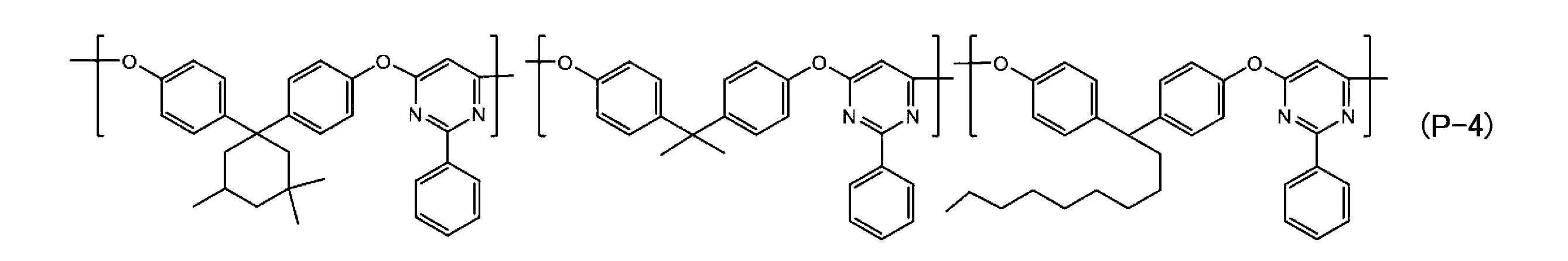
<合成例5>
攪拌装置を備えた四つ口セパラブルフラスコに、1,1-ビス(4-ヒドロキシフェニル)-3,3,5-トリメチルシクロヘキサン(BisTMC)(12.4g、40.0mmol)、4,4’-(1,3-ジメチルブチリデン)ビスフェノール(BisP-MIBK)(2.7g、10.0mmol)、1,1-ビス(4-ヒドロキシフェニル)-ノナン(BisP-DED)(3.3g、10.0mmol)、4,6-ジクロロ-2-フェニルピリミジン(PhPym)(13.7g、61.1mmol)、及び炭酸カリウム(11.4g、82.5mmol)を量り入れ、N-メチル-2-ピロリドン(75g)を加え、窒素雰囲気下、130℃で6時間反応させた。反応終了後、N-メチル-2-ピロリドン(368g)を加えて希釈し、濾過により塩を除去した後、この溶液をメタノール(9.1kg)に投入した。析出した固体を濾別し、少量のメタノールで洗浄し、再度濾別して回収した後、合成例1と同じ条件で乾燥し、下記式(P-5)で表される構造単位を有する重合体P-5を得た(収量23.8g、収率88%、重量平均分子量(Mw);157,000、ガラス転移温度(Tg);190℃)。なお、重量平均分子量及びガラス転移温度は合成例1と同様に測定した。
攪拌装置を備えた四つ口セパラブルフラスコに、1,1-ビス(4-ヒドロキシフェニル)-3,3,5-トリメチルシクロヘキサン(BisTMC)(12.4g、40.0mmol)、4,4’-(1,3-ジメチルブチリデン)ビスフェノール(BisP-MIBK)(2.7g、10.0mmol)、1,1-ビス(4-ヒドロキシフェニル)-ノナン(BisP-DED)(3.3g、10.0mmol)、4,6-ジクロロ-2-フェニルピリミジン(PhPym)(13.7g、61.1mmol)、及び炭酸カリウム(11.4g、82.5mmol)を量り入れ、N-メチル-2-ピロリドン(75g)を加え、窒素雰囲気下、130℃で6時間反応させた。反応終了後、N-メチル-2-ピロリドン(368g)を加えて希釈し、濾過により塩を除去した後、この溶液をメタノール(9.1kg)に投入した。析出した固体を濾別し、少量のメタノールで洗浄し、再度濾別して回収した後、合成例1と同じ条件で乾燥し、下記式(P-5)で表される構造単位を有する重合体P-5を得た(収量23.8g、収率88%、重量平均分子量(Mw);157,000、ガラス転移温度(Tg);190℃)。なお、重量平均分子量及びガラス転移温度は合成例1と同様に測定した。
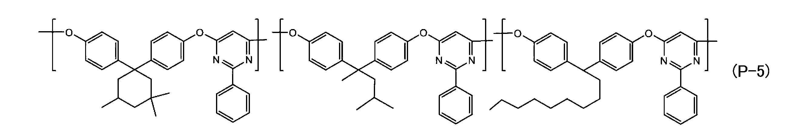
4.2.実施例1
4.2.1.Bステージ樹脂層/剥離層積層体の作製
重合体P-1を50部、硬化性化合物として2,2’-ビス(4-シアナトフェニル)プロパン(東京化成工業社製)を50部、硬化助剤として1-ベンジル-2-メチルイミダゾール(三菱化学社製、製品名「BMI 12」)を5部、及びシクロペンタノンを160部混合し、樹脂層用組成物を調製した。
4.2.1.Bステージ樹脂層/剥離層積層体の作製
重合体P-1を50部、硬化性化合物として2,2’-ビス(4-シアナトフェニル)プロパン(東京化成工業社製)を50部、硬化助剤として1-ベンジル-2-メチルイミダゾール(三菱化学社製、製品名「BMI 12」)を5部、及びシクロペンタノンを160部混合し、樹脂層用組成物を調製した。
剥離層として、厚さ100μmのPETフィルム(帝人フィルムソリューション社製、テイジンテトロンフィルムG2)上に、硬化後の膜厚が25μmとなるように上記で調製した樹脂層用組成物をバーコーターを用いて塗工し、オーブンを用いて70℃で10分加熱した後、さらに130℃で10分加熱して、PETフィルム上にBステージ樹脂層が積層された「Bステージ樹脂層/剥離層積層体」を得た。
<表面粗さRa>
上記で得られた「Bステージ樹脂層/剥離層積層体」の樹脂層の表面を、白色干渉顕微装置(ZYGO社製 New View 5032)を用いて測定し、JIS B0601-2001に準拠して10μm×10μmの範囲について算出した「算術平均粗さ」を表面粗さRaとした。その結果を表1に示す。
上記で得られた「Bステージ樹脂層/剥離層積層体」の樹脂層の表面を、白色干渉顕微装置(ZYGO社製 New View 5032)を用いて測定し、JIS B0601-2001に準拠して10μm×10μmの範囲について算出した「算術平均粗さ」を表面粗さRaとした。その結果を表1に示す。
<樹脂層の50℃~200℃の弾性率測定>
上記で得られた「Bステージ樹脂層/剥離層積層体」から剥離層(PETフィルム)を剥離し、試験片(幅3mm×長さ2cm)を切り出し、DMS試験器(セイコーインスツル社製)にて、1Hz、10℃/分の測定条件で、50℃以上80℃未満の温度範囲での弾性率(MPa)の最大値及び80℃以上200℃以下の温度範囲での弾性率(MPa)の最小値を測定した。その結果を表1に示す。
上記で得られた「Bステージ樹脂層/剥離層積層体」から剥離層(PETフィルム)を剥離し、試験片(幅3mm×長さ2cm)を切り出し、DMS試験器(セイコーインスツル社製)にて、1Hz、10℃/分の測定条件で、50℃以上80℃未満の温度範囲での弾性率(MPa)の最大値及び80℃以上200℃以下の温度範囲での弾性率(MPa)の最小値を測定した。その結果を表1に示す。
4.2.2.金属層/Bステージ樹脂層/剥離層積層体の作製
上記で得られた「Bステージ樹脂層/剥離層積層体」の露出した樹脂層上に、厚さ18μmの銅箔(三井金属社製、型番「TQ-M4-VSP」、表面粗さ110nm)を重ね合わせ、さらに150℃の熱ロールで線荷重10kN/mの条件でプレスし、銅箔/Bステージ樹脂層/PETフィルムの積層構造を有する「金属層/Bステージ樹脂層/剥離層積層体」を作製した。なお、銅箔の表面粗さRaは、白色干渉顕微装置(ZYGO社製 New View 5032)を用いて測定し、JIS B0601-2001に準拠して10μm×10μmの範囲について算出した「算術平均粗さ」を表面粗さRaとした。その結果を表1に示す。
上記で得られた「Bステージ樹脂層/剥離層積層体」の露出した樹脂層上に、厚さ18μmの銅箔(三井金属社製、型番「TQ-M4-VSP」、表面粗さ110nm)を重ね合わせ、さらに150℃の熱ロールで線荷重10kN/mの条件でプレスし、銅箔/Bステージ樹脂層/PETフィルムの積層構造を有する「金属層/Bステージ樹脂層/剥離層積層体」を作製した。なお、銅箔の表面粗さRaは、白色干渉顕微装置(ZYGO社製 New View 5032)を用いて測定し、JIS B0601-2001に準拠して10μm×10μmの範囲について算出した「算術平均粗さ」を表面粗さRaとした。その結果を表1に示す。
<剥離層剥離後の表面粗さRa>
上記で得られた「金属層/Bステージ樹脂層/剥離層積層体」から剥離層(PETフィルム)を剥離し、露出した樹脂層の表面を、白色干渉顕微装置(ZYGO社製 New View 5032)を用いて測定し、JIS B0601-2001に準拠して10μm×10μmの範囲について算出した「算術平均粗さ」を表面粗さRaとした。その結果を表1に示す。
上記で得られた「金属層/Bステージ樹脂層/剥離層積層体」から剥離層(PETフィルム)を剥離し、露出した樹脂層の表面を、白色干渉顕微装置(ZYGO社製 New View 5032)を用いて測定し、JIS B0601-2001に準拠して10μm×10μmの範囲について算出した「算術平均粗さ」を表面粗さRaとした。その結果を表1に示す。
4.2.3.高周波回路用積層体の作製及び評価
上記で得られた「金属層/Bステージ樹脂層/剥離層積層体」から剥離層(PETフィルム)を剥離し、露出した樹脂層面と厚さ18μmの銅箔(三井金属社製、型番「TQ-M4-VSP」、表面粗さ110nm)とを重ね合わせて載置し、150℃の熱ロールで線荷重10kN/mの条件でプレスし、その後オーブンを用いて250℃で3時間加熱して、Cステージ樹脂層の両面に銅箔が積層された「銅箔(膜厚18μm)/Cステージ樹脂層(膜厚25μm)/銅箔(膜厚18μm)」の積層構造を有する高周波回路用積層体を作製した。なお、銅箔(金属層)の表面粗さRaは、白色干渉顕微装置(ZYGO社製 New View 5032)を用いて測定し、JIS B0601-2001に準拠して10μm×10μmの範囲について算出した「算術平均粗さ」を表面粗さRaとした。その結果を表1に示す。
上記で得られた「金属層/Bステージ樹脂層/剥離層積層体」から剥離層(PETフィルム)を剥離し、露出した樹脂層面と厚さ18μmの銅箔(三井金属社製、型番「TQ-M4-VSP」、表面粗さ110nm)とを重ね合わせて載置し、150℃の熱ロールで線荷重10kN/mの条件でプレスし、その後オーブンを用いて250℃で3時間加熱して、Cステージ樹脂層の両面に銅箔が積層された「銅箔(膜厚18μm)/Cステージ樹脂層(膜厚25μm)/銅箔(膜厚18μm)」の積層構造を有する高周波回路用積層体を作製した。なお、銅箔(金属層)の表面粗さRaは、白色干渉顕微装置(ZYGO社製 New View 5032)を用いて測定し、JIS B0601-2001に準拠して10μm×10μmの範囲について算出した「算術平均粗さ」を表面粗さRaとした。その結果を表1に示す。
<引張強度及び引張伸び>
作製した高周波回路用積層体にエッチング処理して銅箔を除去し、評価用樹脂フィルムを作成した。作成した樹脂フィルムからJIS K 7161 7号ダンベル形試験片を切り出し、島津製作所社製「Ez-LX」を用い、5mm/分で引っ張り、破断した際の応力を引張強度、伸びを引張伸びとして測定した。結果を表1に示す。
作製した高周波回路用積層体にエッチング処理して銅箔を除去し、評価用樹脂フィルムを作成した。作成した樹脂フィルムからJIS K 7161 7号ダンベル形試験片を切り出し、島津製作所社製「Ez-LX」を用い、5mm/分で引っ張り、破断した際の応力を引張強度、伸びを引張伸びとして測定した。結果を表1に示す。
<ガラス転移温度(Tg)>
作製した高周波回路用積層体にエッチング処理して銅箔を除去し、評価用樹脂フィルムを作成した。作成した樹脂フィルムから試験片(幅3mm×長さ1cm)を切り出し、DMS試験器(セイコーインスツル社製、型番「EXSTAR4000」)にてガラス転移温度(Tg)を測定した。結果を表1に示す。
作製した高周波回路用積層体にエッチング処理して銅箔を除去し、評価用樹脂フィルムを作成した。作成した樹脂フィルムから試験片(幅3mm×長さ1cm)を切り出し、DMS試験器(セイコーインスツル社製、型番「EXSTAR4000」)にてガラス転移温度(Tg)を測定した。結果を表1に示す。
<弾性率>
作製した高周波回路用積層体にエッチング処理して銅箔を除去し、評価用樹脂フィルムを作成した。作成した樹脂フィルムからJIS K 7161 7号ダンベルを切り出し、島津製作所社製「Ez-LX」を用いて、JIS K 7161に準じて5mm/分で引張試験を行い、引張弾性率を測定した。結果を表1に示す。
作製した高周波回路用積層体にエッチング処理して銅箔を除去し、評価用樹脂フィルムを作成した。作成した樹脂フィルムからJIS K 7161 7号ダンベルを切り出し、島津製作所社製「Ez-LX」を用いて、JIS K 7161に準じて5mm/分で引張試験を行い、引張弾性率を測定した。結果を表1に示す。
<電気特性(比誘電率、誘電正接)>
作製した高周波回路用積層体にエッチング処理して銅箔を除去し、評価用樹脂フィルムを作成した。作成した樹脂フィルムから試験片(幅2.6mm×長さ80mm)を切り出し、空洞共振器摂動法誘電率測定装置(アジレントテクノロジー社製、型番「PNA-LネットワークアナライザーN5230A」、関東電子応用開発社製、型番「空洞共振器10GHz用CP531)を用いて23℃、10GHzにおける比誘電率及び誘電正接の測定を行った。結果を表1に示す。
作製した高周波回路用積層体にエッチング処理して銅箔を除去し、評価用樹脂フィルムを作成した。作成した樹脂フィルムから試験片(幅2.6mm×長さ80mm)を切り出し、空洞共振器摂動法誘電率測定装置(アジレントテクノロジー社製、型番「PNA-LネットワークアナライザーN5230A」、関東電子応用開発社製、型番「空洞共振器10GHz用CP531)を用いて23℃、10GHzにおける比誘電率及び誘電正接の測定を行った。結果を表1に示す。
<剥離強度>
作製した高周波回路用積層体から試験片(幅1cm×長さ10cm)を切り出し、インストロン社製「Instron5567」を用い、500mm/分の条件で90度方向に引っ張り、「IPC-TM-650 2.4.9」に準拠して剥離強度を測定した。結果を表1に示す。
作製した高周波回路用積層体から試験片(幅1cm×長さ10cm)を切り出し、インストロン社製「Instron5567」を用い、500mm/分の条件で90度方向に引っ張り、「IPC-TM-650 2.4.9」に準拠して剥離強度を測定した。結果を表1に示す。
4.2.4.積層体捲回体の作製及び評価
上記で作製した高周波回路用積層体を、幅250mm、巻芯半径40mmの厚紙製の巻芯に厚さ10μmの両面テープを幅方向中央に長さ100mmにわたって貼り付けた。その後、作製した高周波回路用積層体を両面テープに接合した後、巻き取り張力150N/mで巻芯に高周波回路用積層体を1,000層に巻き、積層体捲回体を作製した。
上記で作製した高周波回路用積層体を、幅250mm、巻芯半径40mmの厚紙製の巻芯に厚さ10μmの両面テープを幅方向中央に長さ100mmにわたって貼り付けた。その後、作製した高周波回路用積層体を両面テープに接合した後、巻き取り張力150N/mで巻芯に高周波回路用積層体を1,000層に巻き、積層体捲回体を作製した。
作製した積層体捲回体に捲回された高周波回路用積層体を25℃で1ヶ月保存した後、巻芯から積層体を全て巻き戻した。その後、巻き戻した積層体の巻癖を目視で評価した。巻癖が認められない場合は「良好」と判断し、巻癖が激しく、実用に供することができない場合には「不良」と判断した。結果を表1に示す。
4.2.5.回路基板の作製及び評価
上記で作製した高周波回路用積層体の片面を、感光性ドライフィルムを用いて銅箔をパターニングし、ピッチが150μmで線幅がそれぞれ40、45、50、55、60μm、及びピッチが750μmで線幅がそれぞれ200、220、240、260、280μmの銅配線パターンを作製した。次いで、作製した銅配線パターンの表面に、上記で作製した「Bステージ樹脂層/剥離層積層体」をBステージ樹脂層側がパターニングした高周波回路用積層体の銅配線に接するように載置した後、その上に鏡板を乗せ、120℃/3.0MPa/5分のプレス条件で加熱加圧成形後、剥離層(PETフィルム)を剥離して250℃で3時間加熱して、回路基板を作製した。
上記で作製した高周波回路用積層体の片面を、感光性ドライフィルムを用いて銅箔をパターニングし、ピッチが150μmで線幅がそれぞれ40、45、50、55、60μm、及びピッチが750μmで線幅がそれぞれ200、220、240、260、280μmの銅配線パターンを作製した。次いで、作製した銅配線パターンの表面に、上記で作製した「Bステージ樹脂層/剥離層積層体」をBステージ樹脂層側がパターニングした高周波回路用積層体の銅配線に接するように載置した後、その上に鏡板を乗せ、120℃/3.0MPa/5分のプレス条件で加熱加圧成形後、剥離層(PETフィルム)を剥離して250℃で3時間加熱して、回路基板を作製した。
<伝送損失評価>
上記で作製した回路基板について、測定プローブ(カスケードマイクロテック社製、シングル(ACP40GSG250)、ベクトル型ネットワークアナライザー(Keysight technology E8363B)を用いて25℃における周波数20GHzの伝送損失を測定した。伝送損失が-5dB/100mm以上の場合、良好と判断した。
上記で作製した回路基板について、測定プローブ(カスケードマイクロテック社製、シングル(ACP40GSG250)、ベクトル型ネットワークアナライザー(Keysight technology E8363B)を用いて25℃における周波数20GHzの伝送損失を測定した。伝送損失が-5dB/100mm以上の場合、良好と判断した。
<基板段差評価>
上記で作製した高周波回路用積層体の両面を、銅箔の厚みが9μmになるように両面エッチングを行い、さらに感光性ドライフィルムを用いて銅箔をパターニングし、ピッチが100μmで線幅が50μmの銅配線パターンを作製した。
次に、上記で作製した「金属層/Bステージ樹脂層/剥離層積層体」から、剥離層(PETフィルム)を剥離し、剥離して露出した樹脂層と、作製した銅配線パターンが接するように両面に配置し、さらに鏡板で挟み込み、120℃/1.1MPa/2分のプレス条件で加熱加圧し、さらに250℃で3時間加熱した。
その後、感光性ドライフィルムを用いて銅箔をパターニングし、ピッチが100μmで線幅が50μmの銅配線パターンを両面に作製した。
最後に、上記で作製した「Bステージ樹脂層/剥離層積層体」から、剥離層(PETフィルム)を剥離し、剥離面の樹脂層と、作製した銅配線パターンが接するように両面に配置し、さらに鏡板で挟み込み、120℃/1.1MPa/2分のプレス条件で加熱加圧成形後、さらに250℃で3時間加熱し、4層の銅配線を有する評価用基板を作製した。
作製した評価用基板の断面形状を、走査型電子顕微鏡を用いて観察し、凹部と凸部の差が5%以下の場合、実用可能であり良好と判断、5%超の場合、実用不可でありと不良と判断した。結果を表1に示す。
4.3.実施例2~7、比較例1~3、参考例1
樹脂層用組成物を表1の組成に変更し、金属膜の種類や各種膜厚、積層条件、積層体捲回体の作製条件を表1のように変更した以外は実施例1と同様の方法で高周波回路用積層体を作製し評価した。結果を表1に示す。
樹脂層用組成物を表1の組成に変更し、金属膜の種類や各種膜厚、積層条件、積層体捲回体の作製条件を表1のように変更した以外は実施例1と同様の方法で高周波回路用積層体を作製し評価した。結果を表1に示す。
4.4.実施例8
厚さ18μmの銅箔(三井金属社製、型番「TQ-M4-VSP」、表面粗さ110nm)上に、硬化後の膜厚が25μmとなるように、実施例1で作製した樹脂層用組成物をバーコーターを用いて塗工し、オーブンを用いて70℃で10分間加熱した後、さらに130℃で10分間加熱して、銅箔/Bステージ樹脂層の積層構造を有する「金属層/Bステージ樹脂層積層体」を作製した。
厚さ18μmの銅箔(三井金属社製、型番「TQ-M4-VSP」、表面粗さ110nm)上に、硬化後の膜厚が25μmとなるように、実施例1で作製した樹脂層用組成物をバーコーターを用いて塗工し、オーブンを用いて70℃で10分間加熱した後、さらに130℃で10分間加熱して、銅箔/Bステージ樹脂層の積層構造を有する「金属層/Bステージ樹脂層積層体」を作製した。
作製した「金属層/Bステージ樹脂層積層体」の露出した樹脂層面へ、厚さ18μmの銅箔(三井金属社製、型番「TQ-M4-VSP」、表面粗さ110nm)を重ね合わせ、150℃の熱ロールを用いて線荷重10kN/mの条件でプレスし、その後、オーブンを用いて250℃で3時間加熱し、Cステージ樹脂層の両面に銅箔が積層された、銅箔(膜厚18μm)/Cステージ樹脂層(膜厚25μm)/銅箔(膜厚18μm)の積層構造を有する高周波回路用積層体を作製した。このようにして作製された高周波回路用積層体について、実施例1と同様に評価した。結果を表1に示す。
4.5.比較例4
表1の組成となるように樹脂層用組成物を実施例1と同様に作製し、厚さ18μmの銅箔(三井金属社製、型番「TQ-M4-VSP」、表面粗さ110nm)上に、硬化後の膜厚が25μmとなるように、樹脂層用組成物をバーコーターを用いて塗工し、オーブンを用いて70℃で10分間加熱した後、130℃で10分間加熱し、さらに250℃で3時間加熱した。
表1の組成となるように樹脂層用組成物を実施例1と同様に作製し、厚さ18μmの銅箔(三井金属社製、型番「TQ-M4-VSP」、表面粗さ110nm)上に、硬化後の膜厚が25μmとなるように、樹脂層用組成物をバーコーターを用いて塗工し、オーブンを用いて70℃で10分間加熱した後、130℃で10分間加熱し、さらに250℃で3時間加熱した。
その後、露出した樹脂層表面に銅スパッタを行い、樹脂層の両面に銅層が積層された、銅箔(膜厚18μm)/樹脂層(25μm)/銅層(1μm)の積層構造を有する高周波回路用積層体を作製した。このようにして作製された高周波回路用積層体について、実施例1と同様に評価した。結果を表1に示す。
4.6.比較例5
厚さ25μmポリイミドフィルム(東レ社製、商品名「カプトン100H」)の表面に、接着性層を作製するためにマレイン酸変性スチレン-エチレンブチレン-スチレンブロック共重合体(旭化成ケミカルズ社製、商品名「タフテックM1913」)をロ-ル塗布した。次いで、この塗膜付きフィルムをオーブン内に静置して、100℃で3分間乾燥させて厚さ25μmの被膜(接着性層)を形成し、「接着性層/ポリイミド層積層体」を得た。
その後、厚さ18μmの銅箔(三井金属社製、型番「TQ-M4-VSP」、表面粗さ110nm)の両面を、作製した「接着性層/ポリイミド層積層体」の接着性層の表面に面接触するように重ね合わせて載置し、120℃の熱ロールで線荷重10kN/mの条件でプレスし、その後オーブンを用いて180℃で圧力3MPaの条件で1分間加熱し、その後、180℃で1時間の加熱を行い、ポリイミド層の両面に銅箔が積層された「銅箔(膜厚18μm)/ポリイミド層(膜厚25μm)/銅箔(膜厚18μm)」の積層構造を有する高周波回路用積層体を作製した。このようにして作製された高周波回路用積層体について、実施例1と同様に評価した。結果を表1に示す。
4.7.評価結果
表1に、各実施例及び各比較例で使用した樹脂層用組成物の組成、各層及び高周波回路用積層体及び積層体捲回体の評価結果を示す。
表1に、各実施例及び各比較例で使用した樹脂層用組成物の組成、各層及び高周波回路用積層体及び積層体捲回体の評価結果を示す。

上表1中、下記の略称等について補足する。
<重合体>
・P-6:Sabic社製、型番「PPOレジンパウダー」、ガラス転移温度(Tg);215℃
<硬化性化合物>
・化合物A:2,2’-ビス(4-シアナトフェニル)プロパン(東京化成工業社製)
・化合物B:SR-16H(坂本薬品工業社製、エポキシ当量;160g/eq)
・化合物C:HP-4032D(DIC社製、エポキシ当量;141meq/g)
・化合物D:SR-4PG(坂本薬品工業社製、エポキシ当量;305g/eq)
<硬化助剤>
・硬化助剤A:1-ベンジル-2-メチルイミダゾール(三菱化学社製、製品名「BMI 12」)
・硬化助剤B:2-エチルオクチル酸亜鉛(和光純薬工業社製)
<溶媒>
・溶媒A:シクロペンタノン(東京化成工業社製)
・溶媒B:塩化メチレン(東京化成工業社製)
<金属層種類>
・電解銅箔A:三井金属株式会社製、品番「TQ-M4-VSP」
・電解銅箔B:三井金属株式会社製、品番「3EC-M3S-HTE」
・圧延銅箔A:JX金属株式会社製、品番「GHY5-HA」
表1の結果より、実施例1~8で得られた高周波回路用積層体を用いて回路基板を作成すると、高周波回路における電気信号の伝送損失が低減され、平滑性に優れた回路基板を作製できることがわかった。
また、表1の結果より、実施例1~8で得られた積層体捲回体は、高周波回路における電気信号の伝送損失が低減される高周波回路用積層体を、巻芯に捲回して保管した場合であっても巻癖を効果的に抑制できることがわかった。
10…剥離層、11…樹脂層面(露出面)、12…Bステージ樹脂層、13…樹脂層面(露出面)、14…金属層、16…金属層、18…Cステージ樹脂層、20…金属層、22…Bステージ樹脂層、23…樹脂層面(露出面)、24…金属層、26…Cステージ樹脂層、30…巻芯、32…段差部、40…高周波回路用積層体、41…押し跡(巻癖)、100…高周波回路用積層体、200…高周波回路用積層体、300…積層体捲回体
Claims (8)
- 金属層と、樹脂層とが接して積層され、
前記樹脂層の弾性率が0.1~3GPaであり、
23℃において前記樹脂層の周波数10GHzにおける誘電正接が0.001~0.01であり、かつ、比誘電率が2~3である、高周波回路用積層体。 - 前記樹脂層と前記金属層との剥離強度が5N/cm以上である、請求項1に記載の高周波回路用積層体。
- 前記樹脂層の厚さが10~100μmであり、かつ、前記金属層の厚さが10~50μmである、請求項1または請求項2に記載の高周波回路用積層体。
- 厚さが50~200μmである、請求項1ないし請求項3のいずれか一項に記載の高周波回路用積層体。
- 請求項1ないし請求項4のいずれか一項に記載の高周波回路用積層体を備えたフレキシブルプリント基板。
- 請求項1ないし請求項4のいずれか一項に記載の高周波回路用積層体が、半径10~100mmの巻芯に捲回された、積層体捲回体。
- 表面粗さRaが1~100nmのBステージ樹脂層と、表面粗さRaが10~300nmの金属層とを、50~200℃に加熱して1~19kN/mの線荷重を掛けて貼り合わせる工程を含む、高周波回路積層体の製造方法。
- Bステージ樹脂層と、前記Bステージ樹脂層の少なくとも一方の面に形成された剥離層と、を有するBステージシートであって、
前記Bステージ樹脂層が硬化されてCステージ樹脂層となったときの、
前記Cステージ樹脂層の弾性率が0.1~3GPaであり、
前記Cステージ樹脂層の23℃での周波数10GHzにおける誘電正接が0.001~0.01であり、かつ、比誘電率が2~3である、Bステージシート。
Priority Applications (4)
| Application Number | Priority Date | Filing Date | Title |
|---|---|---|---|
| EP18856178.1A EP3683050A4 (en) | 2017-09-15 | 2018-09-10 | HIGH FREQUENCY CIRCUIT LAMINATE, ITS MANUFACTURING PROCESS, AND STATUS SHEET B |
| KR1020207007167A KR102535310B1 (ko) | 2017-09-15 | 2018-09-10 | 고주파 회로용 적층체 및 그의 제조 방법, 그리고 b 스테이지 시트 |
| CN201880059040.XA CN111093975B (zh) | 2017-09-15 | 2018-09-10 | 高频电路用层叠体及其制造方法、其用途、以及b阶片 |
| US16/647,119 US11134568B2 (en) | 2017-09-15 | 2018-09-10 | High-frequency circuit laminate and method for producing same, and B-stage sheet |
Applications Claiming Priority (4)
| Application Number | Priority Date | Filing Date | Title |
|---|---|---|---|
| JP2017177601 | 2017-09-15 | ||
| JP2017-177601 | 2017-09-15 | ||
| JP2017177600 | 2017-09-15 | ||
| JP2017-177600 | 2017-09-15 |
Publications (1)
| Publication Number | Publication Date |
|---|---|
| WO2019054334A1 true WO2019054334A1 (ja) | 2019-03-21 |
Family
ID=65723597
Family Applications (1)
| Application Number | Title | Priority Date | Filing Date |
|---|---|---|---|
| PCT/JP2018/033477 WO2019054334A1 (ja) | 2017-09-15 | 2018-09-10 | 高周波回路用積層体及びその製造方法、並びにbステージシート |
Country Status (6)
| Country | Link |
|---|---|
| US (1) | US11134568B2 (ja) |
| EP (1) | EP3683050A4 (ja) |
| KR (1) | KR102535310B1 (ja) |
| CN (1) | CN111093975B (ja) |
| TW (1) | TWI783042B (ja) |
| WO (1) | WO2019054334A1 (ja) |
Cited By (3)
| Publication number | Priority date | Publication date | Assignee | Title |
|---|---|---|---|---|
| WO2020179443A1 (ja) * | 2019-03-01 | 2020-09-10 | Jsr株式会社 | 高周波回路用積層体及びその製造方法、フレキシブルプリント基板、bステージシート、並びに積層体捲回体 |
| WO2020217699A1 (ja) * | 2019-04-25 | 2020-10-29 | Jsr株式会社 | 感光性樹脂組成物 |
| WO2022138665A1 (ja) * | 2020-12-21 | 2022-06-30 | 富士フイルム株式会社 | ポリマーフィルム、並びに、積層体及びその製造方法 |
Families Citing this family (3)
| Publication number | Priority date | Publication date | Assignee | Title |
|---|---|---|---|---|
| EP3595033B1 (en) * | 2018-07-10 | 2023-01-04 | Yazaki Corporation | Bus bar module |
| KR20210135140A (ko) | 2020-05-04 | 2021-11-12 | 주식회사 엘지에너지솔루션 | 소화물질을 포함하는 소화부가 구비된 전지 모듈 |
| JP2023020093A (ja) * | 2021-07-30 | 2023-02-09 | 富士フイルム株式会社 | 積層体 |
Citations (17)
| Publication number | Priority date | Publication date | Assignee | Title |
|---|---|---|---|---|
| JP3147706B2 (ja) | 1995-03-22 | 2001-03-19 | 富士写真光機株式会社 | 経皮的に挿入される内視鏡装置 |
| US20080200084A1 (en) * | 2007-02-16 | 2008-08-21 | Angus Richard O | Compositions for thin circuit materials, circuits, multi-layer circuits, and methods of manufacture thereof |
| JP2008284716A (ja) * | 2007-05-15 | 2008-11-27 | Sumitomo Chemical Co Ltd | 高分子フィルム積層体及びその製造方法、並びに、高分子フィルム積層体を用いたフレキシブル配線板。 |
| JP2009231770A (ja) | 2008-03-25 | 2009-10-08 | Nippon Mektron Ltd | 多層フレキシブルプリント配線板およびその製造方法 |
| JP2011040727A (ja) * | 2009-07-14 | 2011-02-24 | Ajinomoto Co Inc | 銅箔付き接着フィルム |
| WO2012014339A1 (ja) | 2010-07-26 | 2012-02-02 | 日本メクトロン株式会社 | フレキシブルプリント配線板及びその製造方法 |
| JP2014197611A (ja) | 2013-03-29 | 2014-10-16 | 東レ・デュポン株式会社 | 高周波回路基板用カバーレイ |
| JP2015176921A (ja) | 2014-03-13 | 2015-10-05 | 東レ・デュポン株式会社 | 高周波回路基板用カバーレイ及びフレキシブルフラットケーブル用基材 |
| JP2015209511A (ja) | 2014-04-28 | 2015-11-24 | Jsr株式会社 | 重合体組成物、重合体ペレット、成形体及びフィルム |
| JP2016032098A (ja) | 2014-07-25 | 2016-03-07 | Jsr株式会社 | 回路基板用樹脂基板、回路基板用樹脂組成物および回路基板 |
| JP2016037045A (ja) * | 2014-08-08 | 2016-03-22 | ポリプラスチックス株式会社 | 金属樹脂積層体及び高周波用配線基板 |
| JP2016087799A (ja) | 2014-10-29 | 2016-05-23 | 東レ・デュポン株式会社 | 高周波回路基板用の長尺状積層体及びその製造方法 |
| WO2016114287A1 (ja) * | 2015-01-13 | 2016-07-21 | 日立化成株式会社 | フレキシブルプリント配線板用樹脂フィルム、樹脂付き金属箔、カバーレイフィルム、ボンディングシート及びフレキシブルプリント配線板 |
| WO2016143447A1 (ja) | 2015-03-11 | 2016-09-15 | Jsr株式会社 | 重合体、樹脂組成物及び樹脂成形体 |
| JP2016183204A (ja) * | 2015-03-25 | 2016-10-20 | Jsr株式会社 | 熱硬化性樹脂組成物およびその用途 |
| JP2017197725A (ja) | 2016-04-20 | 2017-11-02 | Jsr株式会社 | 重合体、組成物及び成形体 |
| JP2018024827A (ja) | 2016-07-28 | 2018-02-15 | Jsr株式会社 | 重合体、組成物及び成形体 |
Family Cites Families (14)
| Publication number | Priority date | Publication date | Assignee | Title |
|---|---|---|---|---|
| JP2001301088A (ja) | 2000-04-24 | 2001-10-30 | Jsr Corp | 積層フィルムおよびその積層フィルムを用いたプリント基板 |
| US7279574B2 (en) | 2003-06-19 | 2007-10-09 | Sumitomo Chemical Company, Limited | Epoxy compound and cured epoxy resin product |
| JP2007262191A (ja) * | 2006-03-28 | 2007-10-11 | Nippon Steel Chem Co Ltd | 難燃硬化性樹脂組成物 |
| JP2008039703A (ja) | 2006-08-09 | 2008-02-21 | Sumitomo Bakelite Co Ltd | 電磁気特性測定治具及び電磁気特性の測定方法 |
| JP4613977B2 (ja) * | 2008-04-28 | 2011-01-19 | 日立化成工業株式会社 | 薄層石英ガラスクロスを含むプリプレグ、およびそれを用いた配線板 |
| TWI393495B (zh) | 2010-12-03 | 2013-04-11 | Adv Flexible Circuits Co Ltd | 訊號傳輸電路板之特性阻抗精度控制結構 |
| WO2012090733A1 (ja) | 2010-12-27 | 2012-07-05 | 株式会社クラレ | 回路基板およびその製造方法 |
| JP5590245B2 (ja) | 2011-08-23 | 2014-09-17 | 日本ゼオン株式会社 | 硬化性樹脂組成物、フィルム、プリプレグ、積層体、硬化物、及び複合体 |
| TWI544843B (zh) | 2011-11-22 | 2016-08-01 | 松下知識產權經營股份有限公司 | 可撓性貼金屬基材、可撓性貼金屬基材之製造方法、印刷配線板、多層可撓印刷配線板、及軟硬複合印刷配線板 |
| KR20140110954A (ko) | 2011-12-22 | 2014-09-17 | 다이요 잉키 세이조 가부시키가이샤 | 드라이 필름 및 그것을 사용한 프린트 배선판, 프린트 배선판의 제조 방법, 및 플립 칩 실장 기판 |
| JP2014070111A (ja) | 2012-09-28 | 2014-04-21 | Nippon Zeon Co Ltd | 絶縁体、絶縁膜、積層体および積層体の製造方法 |
| CN103801501B (zh) | 2014-01-20 | 2016-04-20 | 中国科学院长春应用化学研究所 | 挠性无胶覆铜板及其制备方法 |
| JP6927665B2 (ja) | 2015-12-25 | 2021-09-01 | 日東電工株式会社 | 配線回路基板 |
| KR20190013772A (ko) * | 2016-06-02 | 2019-02-11 | 히타치가세이가부시끼가이샤 | 적층체의 제조 방법 |
-
2018
- 2018-09-10 US US16/647,119 patent/US11134568B2/en active Active
- 2018-09-10 KR KR1020207007167A patent/KR102535310B1/ko active IP Right Grant
- 2018-09-10 CN CN201880059040.XA patent/CN111093975B/zh active Active
- 2018-09-10 WO PCT/JP2018/033477 patent/WO2019054334A1/ja unknown
- 2018-09-10 EP EP18856178.1A patent/EP3683050A4/en active Pending
- 2018-09-14 TW TW107132425A patent/TWI783042B/zh active
Patent Citations (17)
| Publication number | Priority date | Publication date | Assignee | Title |
|---|---|---|---|---|
| JP3147706B2 (ja) | 1995-03-22 | 2001-03-19 | 富士写真光機株式会社 | 経皮的に挿入される内視鏡装置 |
| US20080200084A1 (en) * | 2007-02-16 | 2008-08-21 | Angus Richard O | Compositions for thin circuit materials, circuits, multi-layer circuits, and methods of manufacture thereof |
| JP2008284716A (ja) * | 2007-05-15 | 2008-11-27 | Sumitomo Chemical Co Ltd | 高分子フィルム積層体及びその製造方法、並びに、高分子フィルム積層体を用いたフレキシブル配線板。 |
| JP2009231770A (ja) | 2008-03-25 | 2009-10-08 | Nippon Mektron Ltd | 多層フレキシブルプリント配線板およびその製造方法 |
| JP2011040727A (ja) * | 2009-07-14 | 2011-02-24 | Ajinomoto Co Inc | 銅箔付き接着フィルム |
| WO2012014339A1 (ja) | 2010-07-26 | 2012-02-02 | 日本メクトロン株式会社 | フレキシブルプリント配線板及びその製造方法 |
| JP2014197611A (ja) | 2013-03-29 | 2014-10-16 | 東レ・デュポン株式会社 | 高周波回路基板用カバーレイ |
| JP2015176921A (ja) | 2014-03-13 | 2015-10-05 | 東レ・デュポン株式会社 | 高周波回路基板用カバーレイ及びフレキシブルフラットケーブル用基材 |
| JP2015209511A (ja) | 2014-04-28 | 2015-11-24 | Jsr株式会社 | 重合体組成物、重合体ペレット、成形体及びフィルム |
| JP2016032098A (ja) | 2014-07-25 | 2016-03-07 | Jsr株式会社 | 回路基板用樹脂基板、回路基板用樹脂組成物および回路基板 |
| JP2016037045A (ja) * | 2014-08-08 | 2016-03-22 | ポリプラスチックス株式会社 | 金属樹脂積層体及び高周波用配線基板 |
| JP2016087799A (ja) | 2014-10-29 | 2016-05-23 | 東レ・デュポン株式会社 | 高周波回路基板用の長尺状積層体及びその製造方法 |
| WO2016114287A1 (ja) * | 2015-01-13 | 2016-07-21 | 日立化成株式会社 | フレキシブルプリント配線板用樹脂フィルム、樹脂付き金属箔、カバーレイフィルム、ボンディングシート及びフレキシブルプリント配線板 |
| WO2016143447A1 (ja) | 2015-03-11 | 2016-09-15 | Jsr株式会社 | 重合体、樹脂組成物及び樹脂成形体 |
| JP2016183204A (ja) * | 2015-03-25 | 2016-10-20 | Jsr株式会社 | 熱硬化性樹脂組成物およびその用途 |
| JP2017197725A (ja) | 2016-04-20 | 2017-11-02 | Jsr株式会社 | 重合体、組成物及び成形体 |
| JP2018024827A (ja) | 2016-07-28 | 2018-02-15 | Jsr株式会社 | 重合体、組成物及び成形体 |
Non-Patent Citations (1)
| Title |
|---|
| See also references of EP3683050A4 |
Cited By (9)
| Publication number | Priority date | Publication date | Assignee | Title |
|---|---|---|---|---|
| WO2020179443A1 (ja) * | 2019-03-01 | 2020-09-10 | Jsr株式会社 | 高周波回路用積層体及びその製造方法、フレキシブルプリント基板、bステージシート、並びに積層体捲回体 |
| JPWO2020179443A1 (ja) * | 2019-03-01 | 2020-09-10 | ||
| JP7306449B2 (ja) | 2019-03-01 | 2023-07-11 | Jsr株式会社 | 高周波回路用積層体、フレキシブルプリント基板、及び積層体捲回体 |
| WO2020217699A1 (ja) * | 2019-04-25 | 2020-10-29 | Jsr株式会社 | 感光性樹脂組成物 |
| JPWO2020217699A1 (ja) * | 2019-04-25 | 2020-10-29 | ||
| US20220043345A1 (en) * | 2019-04-25 | 2022-02-10 | Jsr Corporation | Photosensitive resin composition |
| TWI825281B (zh) * | 2019-04-25 | 2023-12-11 | 日商Jsr股份有限公司 | 感光性樹脂組成物、具有圖案的樹脂膜及其製造方法以及半導體電路基板 |
| JP7409374B2 (ja) | 2019-04-25 | 2024-01-09 | Jsr株式会社 | 感光性樹脂組成物 |
| WO2022138665A1 (ja) * | 2020-12-21 | 2022-06-30 | 富士フイルム株式会社 | ポリマーフィルム、並びに、積層体及びその製造方法 |
Also Published As
| Publication number | Publication date |
|---|---|
| CN111093975A (zh) | 2020-05-01 |
| US11134568B2 (en) | 2021-09-28 |
| CN111093975B (zh) | 2022-03-01 |
| KR20200053494A (ko) | 2020-05-18 |
| TWI783042B (zh) | 2022-11-11 |
| EP3683050A1 (en) | 2020-07-22 |
| EP3683050A4 (en) | 2021-06-23 |
| US20200281076A1 (en) | 2020-09-03 |
| KR102535310B1 (ko) | 2023-05-23 |
| TW201932301A (zh) | 2019-08-16 |
Similar Documents
| Publication | Publication Date | Title |
|---|---|---|
| WO2019054334A1 (ja) | 高周波回路用積層体及びその製造方法、並びにbステージシート | |
| WO2019054335A1 (ja) | 回路基板 | |
| TWI777950B (zh) | 聚醯亞胺、聚醯亞胺系黏著劑、薄膜狀黏著材料、黏著層、黏著薄片、附有樹脂之銅箔、覆銅積層板及印刷線路板、以及多層線路板及其製造方法 | |
| JP4986256B2 (ja) | 変性ポリイミド樹脂を含有するプリプレグ | |
| JP4929634B2 (ja) | 接着層付き金属箔及び金属張積層板 | |
| JP2009119855A (ja) | 接着層付き導体箔、導体張積層板、印刷配線板及び多層配線板 | |
| JP7306449B2 (ja) | 高周波回路用積層体、フレキシブルプリント基板、及び積層体捲回体 | |
| JP7115165B2 (ja) | 高周波回路用積層体及びフレキシブルプリント基板 | |
| JP7087859B2 (ja) | 積層体捲回体 | |
| JP5176068B2 (ja) | 導体張積層板、印刷配線板及び多層配線板 | |
| JP5151114B2 (ja) | 接着層付き金属箔、金属張積層板、並びに、この金属張積層板を用いて得られる印刷配線板及び多層配線板 | |
| JP5176069B2 (ja) | 接着層付き金属箔、金属張積層板、印刷配線板及び多層配線板 | |
| JP5408270B2 (ja) | 導体張積層板、印刷配線板及び多層配線板 | |
| JP4815767B2 (ja) | 熱硬化性樹脂組成物及びそれを用いた樹脂ワニス | |
| JP4734867B2 (ja) | 接着層付き金属箔及び金属張積層板 | |
| JP5510498B2 (ja) | 接着層付き金属箔、金属張積層板、並びに、この金属張積層板を用いて得られる印刷配線板及び多層配線板 |
Legal Events
| Date | Code | Title | Description |
|---|---|---|---|
| 121 | Ep: the epo has been informed by wipo that ep was designated in this application |
Ref document number: 18856178 Country of ref document: EP Kind code of ref document: A1 |
|
| NENP | Non-entry into the national phase |
Ref country code: DE |
|
| ENP | Entry into the national phase |
Ref document number: 2018856178 Country of ref document: EP Effective date: 20200415 |